JP7028162B2 - Magnetic recording media, laminates and flexible devices - Google Patents
Magnetic recording media, laminates and flexible devices Download PDFInfo
- Publication number
- JP7028162B2 JP7028162B2 JP2018517077A JP2018517077A JP7028162B2 JP 7028162 B2 JP7028162 B2 JP 7028162B2 JP 2018517077 A JP2018517077 A JP 2018517077A JP 2018517077 A JP2018517077 A JP 2018517077A JP 7028162 B2 JP7028162 B2 JP 7028162B2
- Authority
- JP
- Japan
- Prior art keywords
- layer
- cupping
- recording medium
- substrate
- magnetic recording
- Prior art date
- Legal status (The legal status is an assumption and is not a legal conclusion. Google has not performed a legal analysis and makes no representation as to the accuracy of the status listed.)
- Active
Links
Images

Classifications
-
- G—PHYSICS
- G11—INFORMATION STORAGE
- G11B—INFORMATION STORAGE BASED ON RELATIVE MOVEMENT BETWEEN RECORD CARRIER AND TRANSDUCER
- G11B5/00—Recording by magnetisation or demagnetisation of a record carrier; Reproducing by magnetic means; Record carriers therefor
- G11B5/62—Record carriers characterised by the selection of the material
- G11B5/68—Record carriers characterised by the selection of the material comprising one or more layers of magnetisable material homogeneously mixed with a bonding agent
- G11B5/70—Record carriers characterised by the selection of the material comprising one or more layers of magnetisable material homogeneously mixed with a bonding agent on a base layer
- G11B5/706—Record carriers characterised by the selection of the material comprising one or more layers of magnetisable material homogeneously mixed with a bonding agent on a base layer characterised by the composition of the magnetic material
- G11B5/70605—Record carriers characterised by the selection of the material comprising one or more layers of magnetisable material homogeneously mixed with a bonding agent on a base layer characterised by the composition of the magnetic material metals or alloys
-
- B—PERFORMING OPERATIONS; TRANSPORTING
- B32—LAYERED PRODUCTS
- B32B—LAYERED PRODUCTS, i.e. PRODUCTS BUILT-UP OF STRATA OF FLAT OR NON-FLAT, e.g. CELLULAR OR HONEYCOMB, FORM
- B32B7/00—Layered products characterised by the relation between layers; Layered products characterised by the relative orientation of features between layers, or by the relative values of a measurable parameter between layers, i.e. products comprising layers having different physical, chemical or physicochemical properties; Layered products characterised by the interconnection of layers
- B32B7/02—Physical, chemical or physicochemical properties
- B32B7/022—Mechanical properties
-
- G—PHYSICS
- G11—INFORMATION STORAGE
- G11B—INFORMATION STORAGE BASED ON RELATIVE MOVEMENT BETWEEN RECORD CARRIER AND TRANSDUCER
- G11B5/00—Recording by magnetisation or demagnetisation of a record carrier; Reproducing by magnetic means; Record carriers therefor
- G11B5/62—Record carriers characterised by the selection of the material
- G11B5/73—Base layers, i.e. all non-magnetic layers lying under a lowermost magnetic recording layer, e.g. including any non-magnetic layer in between a first magnetic recording layer and either an underlying substrate or a soft magnetic underlayer
- G11B5/735—Base layers, i.e. all non-magnetic layers lying under a lowermost magnetic recording layer, e.g. including any non-magnetic layer in between a first magnetic recording layer and either an underlying substrate or a soft magnetic underlayer characterised by the back layer
-
- G—PHYSICS
- G11—INFORMATION STORAGE
- G11B—INFORMATION STORAGE BASED ON RELATIVE MOVEMENT BETWEEN RECORD CARRIER AND TRANSDUCER
- G11B5/00—Recording by magnetisation or demagnetisation of a record carrier; Reproducing by magnetic means; Record carriers therefor
- G11B5/74—Record carriers characterised by the form, e.g. sheet shaped to wrap around a drum
- G11B5/78—Tape carriers
Description
本技術は、磁気記録媒体、積層体およびフレキシブルデバイスに関する。詳しくは、強化層を備える磁気記録媒体、積層体およびフレキシブルデバイスに関する。 The present technology relates to magnetic recording media, laminates and flexible devices. More specifically, the present invention relates to a magnetic recording medium having a reinforcing layer, a laminated body, and a flexible device.
近年、インターネットの普及やビッグデータ解析により情報量が爆発的に増大しており、それら情報をデータとしてバックアップおよびアーカイブしておくための記録媒体には、さらなる高容量化が望まれている。数あるストレージシステムの中でも、磁気テープは低ビットコストとグリーンストレージとして、最近見直されつつある。磁気テープの高密度化は、近年148ギガビット毎平方インチの世界記録が樹立されとどまるところを知らない。 In recent years, the amount of information has increased exponentially due to the spread of the Internet and big data analysis, and it is desired to further increase the capacity of a recording medium for backing up and archiving such information as data. Among the many storage systems, magnetic tape has recently been reviewed for its low bit cost and green storage. The densification of magnetic tapes has never stopped setting a world record of 148 gigabs per square inch in recent years.
リールに巻かれた状態でカートリッジに収納される磁気テープにおいては、高容量化のために磁気抵抗型ヘッドを多数配した固定ヘッドを用い、テープの長手方向に記録再生が行われるリニア記録方式のLTO(Linear-Tape-Open)などのシステムが実用化されている。さらなる高容量化に向けて、塗布型磁性記録層の磁性粉開発やスパッタ磁性層などの記録層の開発が活発に行われている。これによって、記録ビット長を狭くしてテープの長手方向の記録密度(一般には線記録密度)を向上させることが可能となる。 For magnetic tapes that are wound in a reel and stored in a cartridge, a fixed head with a large number of magnetoresistive heads is used to increase the capacity, and recording and playback are performed in the longitudinal direction of the tape. Systems such as LTO (Linear-Tape-Open) have been put into practical use. To further increase the capacity, the development of magnetic powder for a coating type magnetic recording layer and the development of a recording layer such as a sputter magnetic layer are being actively carried out. This makes it possible to narrow the recording bit length and improve the recording density in the longitudinal direction of the tape (generally, the linear recording density).
一方、磁気テープは磁気ディスクと比較して、フレキシブルなフィルム状の基体を用いるため、記録トラック幅が非常に広い。磁気テープの高密度化は前述の記録層の開発とともに、テープ幅方向のトラック密度の向上ができれば、飛躍的に記録密度が向上する。この場合、線記録密度がかわらないため、磁性記録層とヘッドとのわずかなスペーシングにより出力が小さくなることが緩和されるなど、高トラック密度化の技術開発はテープドライブの開発にメリットが大きいと思われる。 On the other hand, since the magnetic tape uses a flexible film-like substrate as compared with the magnetic disk, the recording track width is very wide. If the track density in the tape width direction can be improved along with the development of the recording layer described above, the density of the magnetic tape will be dramatically improved. In this case, since the line recording density does not change, it is alleviated that the output becomes small due to a slight spacing between the magnetic recording layer and the head. I think that the.
現在の磁気テープにおいて、テープ幅方向のトラック密度を上げると、テープ走行時の幅方向の変動や温度湿度などの環境要因によるテープ自体の寸法変化により、本来磁気ヘッドが読み取るべきトラック位置にトラックが存在しない、もしくはずれたトラック位置を読み取るなどのいわゆるオフトラックが発生してしまう。高密度化のためにテープの厚みが薄くなるに伴い、テンション要因によるテープ幅の変化がさらに大きくなるので、オフトラックの影響が顕著になりテープ走行性が不安定になっていく可能性もある。 With the current magnetic tape, if the track density in the tape width direction is increased, the track will move to the track position that the magnetic head should read due to changes in the dimensions of the tape itself due to environmental factors such as fluctuations in the width direction during tape running and temperature and humidity. So-called off-tracks such as reading the track positions that do not exist or are out of alignment occur. As the thickness of the tape becomes thinner due to the higher density, the change in the tape width due to the tension factor becomes larger, so the influence of off-track becomes remarkable and the tape running performance may become unstable. ..
これに対して、片面または両面に金属、合金、またはその酸化物からなる強化層を基体に設けて、基体を補強する技術が提案されている(例えば、特許文献1~6参照。)。 On the other hand, a technique has been proposed in which a reinforcing layer made of a metal, an alloy, or an oxide thereof is provided on one side or both sides of the substrate to reinforce the substrate (see, for example, Patent Documents 1 to 6).
しかしながら、補強層を基体に設けると、テープの形状が幅方向に湾曲するいわゆるカッピングが増大する。これにより書き込みおよび読みだしを行う磁気ヘッドと磁気テープとの間にスペーシングが生じ、記録再生特性が劣化することになる。このため、寸法安定性に優れ、かつカッピングを抑制できる磁気テープが望まれている。 However, when the reinforcing layer is provided on the substrate, so-called cupping in which the shape of the tape is curved in the width direction increases. As a result, spacing occurs between the magnetic head for writing and reading and the magnetic tape, and the recording / reproducing characteristics are deteriorated. Therefore, a magnetic tape having excellent dimensional stability and capable of suppressing cupping is desired.
また、フレキシブルデバイスなどにおいても、磁気テープにおけるのと同様に、寸法安定性に優れ、かつ湾曲を抑制できるものが望まれている。 Further, even in a flexible device or the like, a device having excellent dimensional stability and capable of suppressing bending is desired, as in the case of a magnetic tape.
したがって、本技術の第1の目的は、寸法安定性に優れ、かつカッピングを抑制できる磁気記録媒体を提供することにある。 Therefore, the first object of the present technology is to provide a magnetic recording medium having excellent dimensional stability and capable of suppressing cupping.
また、本技術の第2の目的は、寸法安定性に優れ、かつ湾曲を抑制できる積層体およびフレキシブルデバイスを提供することにある。 A second object of the present technology is to provide a laminated body and a flexible device which are excellent in dimensional stability and can suppress bending.
上述の課題を解決するために、第1の技術は、
長尺状の基体と、
基体の一方の面上に設けられた強化層およびカッピング抑制層と
を備え、
強化層が、
第1の金属酸化物層と、
第2の金属酸化物層と、
第1の金属酸化物層および第2の金属酸化物層の間に設けられた金属層と
を備える磁気記録媒体である。
In order to solve the above-mentioned problems, the first technology is
With a long substrate,
It is provided with a reinforcing layer and a cupping suppressing layer provided on one surface of the substrate .
The strengthening layer,
The first metal oxide layer and
The second metal oxide layer and
With the metal layer provided between the first metal oxide layer and the second metal oxide layer
It is a magnetic recording medium provided with.
第2の技術は、
基体と、
基体の一方の面上に設けられた強化層およびカッピング抑制層と
を備え、
強化層が、
第1の金属酸化物層と、
第2の金属酸化物層と、
第1の金属酸化物層および第2の金属酸化物層の間に設けられた金属層と
を備える積層体である。
The second technology is
With the substrate
It is provided with a reinforcing layer and a cupping suppressing layer provided on one surface of the substrate .
The strengthening layer,
The first metal oxide layer and
The second metal oxide layer and
With the metal layer provided between the first metal oxide layer and the second metal oxide layer
It is a laminated body provided with.
第3の技術は、第2の技術の積層体を備えるフレキシブルデバイスである。 The third technique is a flexible device comprising the laminate of the second technique.
以上説明したように、本技術によれば、寸法安定性に優れ、かつカッピングを抑制できる磁気記録媒体を実現できる。また、寸法安定性に優れ、かつ湾曲を抑制できる積層体を実現できる。 As described above, according to the present technology, it is possible to realize a magnetic recording medium having excellent dimensional stability and capable of suppressing cupping. In addition, it is possible to realize a laminated body having excellent dimensional stability and suppressing bending.
本技術の実施形態について以下の順序で説明する。
1 第1の実施形態(磁気記録媒体の例)
1.1 磁気記録媒体の構成
1.2 磁気記録媒体の製造方法
1.3 効果
1.4 変形例
2 第2の実施形態(ディスプレイの例)
2.1 ディスプレイの構成
2.2 効果
2.3 変形例The embodiments of the present technology will be described in the following order.
1 First embodiment (example of magnetic recording medium)
1.1 Configuration of magnetic recording medium 1.2 Manufacturing method of magnetic recording medium 1.3 Effect 1.4 Modification example 2 Second embodiment (example of display)
2.1 Display configuration 2.2 Effect 2.3 Modification example
<1 第1の実施形態>
[1.1 磁気記録媒体の構成]
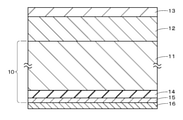
本技術の第1の実施形態に係る磁気記録媒体は、いわゆる塗布型の垂直磁気記録媒体であり、図1に示すように、長尺状の基体11と、基体11の一方の面上に設けられた下地層12と、下地層12上に設けられた記録層13と、基体11の他方の面上に設けられた強化層14と、強化層14上に設けられたカッピング抑制層15と、カッピング抑制層15上に設けられたバック層16とを備える。また、磁気記録媒体が、必要に応じて、記録層13上に設けられた保護層および潤滑剤層などをさらに備えるようにしてもよい。基体11、強化層14およびカッピング抑制層15により積層体10が構成される。<1 First Embodiment>
[1.1 Configuration of magnetic recording medium]
The magnetic recording medium according to the first embodiment of the present technology is a so-called coating type perpendicular magnetic recording medium, and is provided on one surface of a
磁気記録媒体は、長尺状を有する。磁気記録媒体の長手方向のヤング率が、好ましくは7GPa以上14GPa以下である。ヤング率が7GPa以上であると、良好な磁気ヘッド当たりを得ることができ、かつ、エッジダメージを抑制することができる。一方、ヤング率が14GPa以下であると、良好な磁気ヘッド当たりを得ることができる。 The magnetic recording medium has a long shape. The Young's modulus in the longitudinal direction of the magnetic recording medium is preferably 7 GPa or more and 14 GPa or less. When Young's modulus is 7 GPa or more, good magnetic head contact can be obtained and edge damage can be suppressed. On the other hand, when Young's modulus is 14 GPa or less, good magnetic head contact can be obtained.
磁気記録媒体の湿度膨張係数が、好ましくは0.5ppm/%RH以上、4ppm/%RH以下である。湿度膨張係数が上記範囲であると、磁気記録媒体の寸法安定性をさらに向上できる。 The humidity expansion coefficient of the magnetic recording medium is preferably 0.5 ppm /% RH or more and 4 ppm /% RH or less. When the humidity expansion coefficient is in the above range, the dimensional stability of the magnetic recording medium can be further improved.
(基体)
基体11は、いわゆる非磁性支持体であり、具体的には、可撓性を有する長尺状のフィルムである。基体11の厚みは、例えば、10μm以下である。基体11は、例えば、ポリエステル類、ポリオレフィン類、セルロース誘導体、ビニル系樹脂、ポリイミド類、ポリアミド類、およびポリカーボネートのうちの少なくとも1種を含んでいる。なお、基体11は、単層構造を有していてもよいし、積層構造を有していてもよい。(Hypokeimenon)
The
(下地層)
下地層12は、非磁性粉および結着剤を含む非磁性層である。下地層12が、必要に応じて、導電性粒子、潤滑剤、研磨剤、硬化剤および防錆剤などの各種添加剤をさらに含んでいてもよい。(Underground layer)
The
非磁性粉は、無機物質でも有機物質でもよい。また、カーボンブラックなども使用できる。無機物質としては、例えば、金属、金属酸化物、金属炭酸塩、金属硫酸塩、金属窒化物、金属炭化物、金属硫化物などが挙げられる。非磁性粉の形状としては、例えば、針状、球状、板状などの各種形状が挙げられるが、これに限定されるものではない。 The non-magnetic powder may be an inorganic substance or an organic substance. Also, carbon black or the like can be used. Examples of the inorganic substance include metals, metal oxides, metal carbonates, metal sulfates, metal nitrides, metal carbides, metal sulfides and the like. Examples of the shape of the non-magnetic powder include, but are not limited to, various shapes such as a needle shape, a spherical shape, and a plate shape.
結着剤としては、ポリウレタン系樹脂、塩化ビニル系樹脂などに架橋反応を付与した構造の樹脂が好ましい。しかしながら結着剤はこれらに限定されるものではなく、磁気記録媒体に対して要求される物性などに応じて、その他の樹脂を適宜配合してもよい。配合する樹脂としては、通常、塗布型の磁気記録媒体において一般的に用いられる樹脂であれば、特に限定されない。 As the binder, a resin having a structure in which a cross-linking reaction is imparted to a polyurethane-based resin, a vinyl chloride-based resin, or the like is preferable. However, the binder is not limited to these, and other resins may be appropriately blended depending on the physical characteristics required for the magnetic recording medium and the like. The resin to be blended is not particularly limited as long as it is a resin generally used in a coating type magnetic recording medium.
例えば、ポリ塩化ビニル、ポリ酢酸ビニル、塩化ビニル-酢酸ビニル共重合体、塩化ビニル-塩化ビニリデン共重合体、塩化ビニル-アクリロニトリル共重合体、アクリル酸エステル-アクリロニトリル共重合体、アクリル酸エステル-塩化ビニル-塩化ビニリデン共重合体、塩化ビニル-アクリロニトリル共重合体、アクリル酸エステル-アクリロニトリル共重合体、アクリル酸エステル-塩化ビニリデン共重合体、メタクリル酸エステル-塩化ビニリデン共重合体、メタクリル酸エステル-塩化ビニル共重合体、メタクリル酸エステル-エチレン共重合体、ポリ弗化ビニル、塩化ビニリデン-アクリロニトリル共重合体、アクリロニトリル-ブタジエン共重合体、ポリアミド樹脂、ポリビニルブチラール、セルロース誘導体(セルロースアセテートブチレート、セルロースダイアセテート、セルローストリアセテート、セルロースプロピオネート、ニトロセルロース)、スチレンブタジエン共重合体、ポリエステル樹脂、アミノ樹脂、合成ゴムなどが挙げられる。 For example, polyvinyl chloride, polyvinyl acetate, vinyl chloride-vinyl acetate copolymer, vinyl chloride-vinylidene chloride copolymer, vinyl chloride-acrylonitrile copolymer, acrylic acid ester-acrylonitrile copolymer, acrylic acid ester-chloride. Vinyl-vinylidene chloride copolymer, vinyl chloride-acrylonitrile copolymer, acrylic acid ester-acrylonitrile copolymer, acrylic acid ester-vinylidene chloride copolymer, methacrylic acid ester-vinylidene chloride copolymer, methacrylic acid ester-chloride Vinyl copolymer, methacrylic acid ester-ethylene copolymer, polyfluorinated vinyl, vinylidene chloride-acrylonitrile copolymer, acrylonitrile-butadiene copolymer, polyamide resin, polyvinyl butyral, cellulose derivative (cellulose acetate butyrate, cellulose die) Acetate, cellulose triacetate, cellulose propionate, nitrocellulose), styrene butadiene copolymer, polyester resin, amino resin, synthetic rubber and the like.
また、熱硬化性樹脂、または反応型樹脂の例としては、フェノール樹脂、エポキシ樹脂、尿素樹脂、メラミン樹脂、アルキッド樹脂、シリコーン樹脂、ポリアミン樹脂、尿素ホルムアルデヒド樹脂などが挙げられる。 Examples of the thermosetting resin or the reactive resin include phenol resin, epoxy resin, urea resin, melamine resin, alkyd resin, silicone resin, polyamine resin, urea formaldehyde resin and the like.
また、上述した各結着剤には、磁性粉の分散性を向上させる目的で、-SO3M、-OSO3M、-COOM、P=O(OM)2などの極性官能基が導入されていてもよい。ここで、式中Mは、水素原子、あるいはリチウム、カリウム、ナトリウムなどのアルカリ金属である。Further, in each of the above-mentioned binders, polar functional groups such as -SO 3 M, -OSO 3 M, -COOM, and P = O (OM) 2 are introduced for the purpose of improving the dispersibility of the magnetic powder. May be. Here, M in the formula is a hydrogen atom or an alkali metal such as lithium, potassium, or sodium.
更に、極性官能基としては、-NR1R2、-NR1R2R3+X-の末端基を有する側鎖型のもの、>NR1R2+X-の主鎖型のものが挙げられる。ここで、式中R1、R2、R3は、水素原子、または炭化水素基であり、X-は弗素、塩素、臭素、ヨウ素などのハロゲン元素イオン、または無機もしくは有機イオンである。また、極性官能基としては、-OH、-SH、-CN、エポキシ基なども挙げられる。Further, examples of the polar functional group include a side chain type having a terminal group of -NR1R2 and -NR1R2R3 + X-, and a main chain type having> NR1R2 + X-. Here, R1, R2, and R3 in the formula are hydrogen atoms or hydrocarbon groups, and X - is a halogen element ion such as fluorine, chlorine, bromine, or iodine, or an inorganic or organic ion. Further, examples of the polar functional group include -OH, -SH, -CN, and an epoxy group.
また、樹脂にポリイソシアネートを併用して、これを架橋硬化させるようにしてもよい。ポリイソシアネートとしては、例えば、トルエンジイソシアネート、およびこれらの付加体、アルキレンジイソシアネート、およびこれらの付加体などが挙げられる。 Further, polyisocyanate may be used in combination with the resin to be crosslinked and cured. Examples of the polyisocyanate include toluene diisocyanates and their adducts, alkylene diisocyanates, and adducts thereof.
導電性粒子としては、炭素を主成分とする微粒子、例えば、カーボンブラックを用いることができる。カーボンブラックとしては、例えば、旭カーボン社の旭#15、#15HSなどを用いることができる。また、シリカ粒子表面にカーボンを付着させたハイブリッドカーボンを用いてもよい。
As the conductive particles, fine particles containing carbon as a main component, for example, carbon black can be used. As the carbon black, for example,
潤滑剤としては、例えば、炭素数10~24の一塩基性脂肪酸と、炭素数2~12の1価~6価アルコールのいずれかとのエステル、これらの混合エステル、またはジ脂肪酸エステル、トリ脂肪酸エステルを適宜用いることができる。潤滑剤の具体例としては、ラウリン酸、ミリスチン酸、パルミチン酸、ステアリン酸、ベヘン酸、オレイン酸、リノール酸、リノレン酸、エライジン酸、ステアリン酸ブチル、ステアリン酸ペンチル、ステアリン酸ヘプチル、ステアリン酸オクチル、ステアリン酸イソオクチル、ミリスチン酸オクチルなどが挙げられる。 Examples of the lubricant include an ester of a monobasic fatty acid having 10 to 24 carbon atoms and any of monohydric to hexahydric alcohols having 2 to 12 carbon atoms, a mixed ester thereof, a difatty acid ester, and a trifatty acid ester. Can be used as appropriate. Specific examples of the lubricant include lauric acid, myristic acid, palmitic acid, stearic acid, behenic acid, oleic acid, linoleic acid, linolenic acid, elladic acid, butyl stearate, pentyl stearate, heptyl stearate, and octyl stearate. , Isooctyl stearate, octyl myristate and the like.
研磨剤としては、例えば、α化率90%以上のα-アルミナ、β-アルミナ、γ-アルミナ、炭化ケイ素、酸化クロム、酸化セリウム、α-酸化鉄、コランダム、窒化珪素、チタンカーバイト、酸化チタン、二酸化珪素、酸化スズ、酸化マグネシウム、酸化タングステン、酸化ジルコニウム、窒化ホウ素、酸化亜鉛、炭酸カルシウム、硫酸カルシウム、硫酸バリウム、2硫化モリブデン、磁性酸化鉄の原料を脱水、アニール処理した針状α酸化鉄、および必要によりそれらをアルミおよび/またはシリカで表面処理したものなどが、単独または組み合せで使用される。 Examples of the polishing agent include α-alumina, β-alumina, γ-alumina, silicon carbide, chromium oxide, cerium oxide, α-iron oxide, corundum, silicon nitride, titanium carbide, and oxidation having an pregelatinization rate of 90% or more. Needle-shaped α obtained by dehydrating and annealing raw materials of titanium, silicon dioxide, tin oxide, magnesium oxide, tungsten oxide, zirconium oxide, boron nitride, zinc oxide, calcium carbonate, calcium sulfate, barium sulfate, molybdenum disulfide, and magnetic iron oxide. Iron oxides, and optionally those surface-treated with aluminum and / or silica, are used alone or in combination.
(記録層)
記録層13は、例えば、短波長記録または超短波超記録が可能な垂直記録層である。記録層13は、記録層13の厚さ方向に磁気異方性を有する磁性層である。すなわち、記録層13の磁化容易軸は、記録層13の厚さ方向に向いている。記録層13の平均厚さは、好ましくは30nm以上100nm以下、より好ましくは50nm以上70nm以下である。(Recording layer)
The
記録層13は、例えば、磁性粉および結着剤を含む磁性層である。記録層13が、必要に応じて、導電性粒子、潤滑剤、研磨剤、硬化剤および防錆剤などの各種添加剤をさらに含んでいてもよい。
The
磁性粉は、例えば、六方晶フェライト磁性粉または立方晶フェライト磁性粉である。六方晶フェライト磁性粉は、六方晶フェライトを主相とする鉄酸化物の磁性粒子(以下「六方晶フェライト磁性粒子」という。)からなる。六方晶フェライトは、例えば、Ba、Sr、PbおよびCaからなる群より選ばれる1種以上を含んでいる。六方晶フェライトは、好ましくは、Baを含むバリウムフェライトである。バリウムフェライトが、Ba以外にSr、PbおよびCaからなる群より選ばれる1種以上をさらに含んでいてもよい。 The magnetic powder is, for example, hexagonal ferrite magnetic powder or cubic ferrite magnetic powder. The hexagonal ferrite magnetic powder is composed of magnetic particles of iron oxide having hexagonal ferrite as the main phase (hereinafter referred to as "hexagonal ferrite magnetic particles"). Hexagonal ferrite contains, for example, one or more selected from the group consisting of Ba, Sr, Pb and Ca. The hexagonal ferrite is preferably a barium ferrite containing Ba. In addition to Ba, barium ferrite may further contain one or more selected from the group consisting of Sr, Pb and Ca.
より具体的には、六方晶フェライトは、一般式MFe12O19で表される平均組成を有する。但し、Mは、例えば、Ba、Sr、PbおよびCaからなる群より選ばれる1種以上の金属である。Mは、好ましくは、Baである。Mが、Baと、Sr、PbおよびCaからなる群より選ばれる1種以上の金属との組み合わせであってもよい。上記一般式においてFeの一部が他の金属元素で置換されていてもよい。More specifically, the hexagonal ferrite has an average composition represented by the general formula MFe 12 O 19 . However, M is one or more metals selected from the group consisting of, for example, Ba, Sr, Pb and Ca. M is preferably Ba. M may be a combination of Ba and one or more metals selected from the group consisting of Sr, Pb and Ca. In the above general formula, a part of Fe may be substituted with another metal element.
六方晶フェライト磁性粒子の平均粒径(平均板径)は、好ましくは32nm以下、より好ましくは15nm以上32nm以下である。六方晶フェライト磁性粒子の平均粒子厚は、好ましくは9nm以下、より好ましくは7nm以上9nm以下である。六方晶フェライト磁性粒子の平均アスペクト比(平均粒径/平均粒子厚)は、好ましくは3.9以下、より好ましくは1.9以上3.9以下である。 The average particle size (average plate diameter) of the hexagonal ferrite magnetic particles is preferably 32 nm or less, more preferably 15 nm or more and 32 nm or less. The average particle thickness of the hexagonal ferrite magnetic particles is preferably 9 nm or less, more preferably 7 nm or more and 9 nm or less. The average aspect ratio (average particle size / average particle thickness) of the hexagonal ferrite magnetic particles is preferably 3.9 or less, more preferably 1.9 or more and 3.9 or less.
立方晶フェライト磁性粉は、立方晶フェライトを主相とする鉄酸化物の磁性粒子(以下「立方晶フェライト磁性粒子」という。)からなる。立方晶フェライトは、Co、Ni、Mn、Al、CuおよびZnからなる群より選ばれる1種以上を含んでいる。好ましくは、立方晶フェライトは、Coを少なくとも含み、Co以外にNi、Mn、Al、CuおよびZnからなる群より選ばれる1種以上をさらに含んでいる。より具体的には例えば、立方晶フェライトは、一般式MFe2O4で表される平均組成を有する。但し、Mは、Co、Ni、Mn、Al、CuおよびZnからなる群より選ばれる1種以上の金属である。好ましくは、Mは、Coと、Ni、Mn、Al、CuおよびZnからなる群より選ばれる1種以上の金属との組み合わせである。The cubic ferrite magnetic powder is composed of magnetic particles of iron oxide having cubic ferrite as a main phase (hereinafter referred to as "cubic ferrite magnetic particles"). The cubic ferrite contains one or more selected from the group consisting of Co, Ni, Mn, Al, Cu and Zn. Preferably, the cubic ferrite contains at least Co, and further contains at least one selected from the group consisting of Ni, Mn, Al, Cu and Zn in addition to Co. More specifically, for example, cubic ferrite has an average composition represented by the general formula MFe 2 O 4 . However, M is one or more metals selected from the group consisting of Co, Ni, Mn, Al, Cu and Zn. Preferably, M is a combination of Co and one or more metals selected from the group consisting of Ni, Mn, Al, Cu and Zn.
立方晶フェライト磁性粒子の平均板径(平均粒子サイズ)は、好ましくは14nm以下、より好ましくは10nm以上14nm以下である。立方晶フェライト磁性粒子の平均板状比(平均アスペクト比(平均板径LAM/平均板厚LBM))は、0.75以上1.25以下であることが好ましい。The average plate diameter (average particle size) of the cubic ferrite magnetic particles is preferably 14 nm or less, more preferably 10 nm or more and 14 nm or less. The average plate-like ratio (average aspect ratio (average plate diameter L AM / average plate thickness L BM )) of the cubic ferrite magnetic particles is preferably 0.75 or more and 1.25 or less.
結着剤は、上述の下地層12と同様である。導電性粒子、潤滑剤および研磨剤も、上述の下地層12と同様である。
The binder is the same as the above-mentioned
記録層13は、非磁性補強粒子として、酸化アルミニウム(α、βまたはγアルミナ)、酸化クロム、酸化珪素、ダイヤモンド、ガーネット、エメリー、窒化ホウ素、チタンカーバイト、炭化珪素、炭化チタン、酸化チタン(ルチル型またはアナターゼ型の酸化チタン)などをさらに含んでいてもよい。
The
(強化層)
強化層14は、磁気記録媒体の機械的強度を高めて、優れた寸法安定性を得るためのものである。強化層14は、例えば、金属および金属化合物のうちの少なくとも1種を含んでいる。ここで、金属には、半金属が含まれるものと定義する。金属は、例えば、アルミニウムおよび銅のうちの少なくとも1種であり、好ましくは銅である。銅は、安価で蒸気圧が比較的低いため、安価に強化層14を成膜が可能であるからである。金属は、例えば、アルミニウム、銅、シリコンおよびコバルトのうちの少なくとも1種であってもよい。金属化合物は、例えば、金属酸化物である。金属酸化物は、例えば、酸化アルミニウム、酸化銅および酸化シリコンのうちの少なくとも1種であり、好ましくは酸化銅である。蒸着法などにより安価に強化層14を成膜が可能であるからである。金属酸化物は、例えば、酸化アルミニウム、酸化銅、酸化シリコンおよび酸化コバルトのうちの少なくとも1種であってもよい。強化層14は、例えば、真空斜方蒸着法により形成される蒸着膜であってもよいし、スパッタ法により形成されるスパッタ膜であってもよい。(Reinforcement layer)
The reinforcing
強化層14は、2層以上の積層構造を有していることが好ましい。強化層14の厚みを厚くしていくと、外力に対する基体11の伸縮をより抑えることができる。しかしながら、蒸着法やスパッタリングなどの真空薄膜の作製技術を用いて強化層14を形成する場合、上記のように強化層14の厚みを厚くしていくと、強化層14中に空隙が生じやすくなる虞がある。上記のように強化層14を2層以上の積層構造とすることで、真空薄膜の作製技術を用いて強化層14を形成する際に強化層14中に生じる空隙を抑制し、強化層14の緻密性を向上できる。したがって、強化層14の水蒸気透過率を低減できるので、基体11の膨張をさらに抑制し、磁気記録媒体の寸法安定性をさらに向上できる。強化層14が2層以上の積層構造を有する場合、各層の材料は同一であってもよいし、異なっていてもよい。
The reinforcing
強化層14の平均厚みは、好ましくは150nm以上500nm以下である。強化層14の平均厚みが150nm以上であると、強化層14として良好な機能(すなわち磁気記録媒体の良好な寸法安定性)が得られる。一方、強化層14の平均厚みを500nmを超えて厚くしなくとも、強化層14として十分な機能が得られる。また、強化層14の平均厚みを500nmを超えて厚くすると、カッピングの発生を抑制するためには、カッピング抑制層15の平均厚みを厚くしなければならなくなり、強化層14とカッピング抑制層15との合計の平均厚みが厚くなりすぎる虞がある。
The average thickness of the reinforcing
強化層14の平均厚みは以下のようにして求められる。まず、磁気記録媒体をその主面に対して垂直に切り出し、その断面を透過型電子顕微鏡(Transmission Electron Microscope:TEM)により観察する。
以下に、TEMの測定条件を示す。
装置:TEM(日立製作所製、H9000NAR)
加速電圧:300kV
倍率:100000倍
次に、観察したTEM像から強化層14の平均厚みを算出する。具体的には、一般財団法人材料科学技術振興財団作製のSEM/TEM測長ソフト、Image Measuring Toolを用いてヒストグラムをとって強化層14の平均厚みを算出する。The average thickness of the reinforcing
The measurement conditions of TEM are shown below.
Equipment: TEM (Hitachi, H9000NAR)
Acceleration voltage: 300kV
Magnification: 100,000 times Next, the average thickness of the reinforcing
強化層14の平均厚みが150nm以上500nm以下である場合、強化層14の平均厚みD1に対するカッピング抑制層15の平均厚みD2の比率(D2/D1)が、0.05以上0.7以下であることが好ましい。比率(D2/D1)が0.05以上であると、強化層14の平均厚みD1に対してカッピング抑制層15の平均厚みD2が十分な平均厚みとなるため、カッピング抑制効果を向上できる。一方、比率(D2/D1)が0.7以下であると、強化層14の平均厚みD1に対してカッピング抑制層15の平均厚みD2が厚くなりすぎないため、カッピング抑制効果を向上できる。
When the average thickness of the reinforcing
(カッピング抑制層)
カッピング抑制層15は、基体11上に強化層14を形成したことにより発生するカッピングを抑制するためのものである。ここで、カッピングとは、長尺状の基体11の幅方向に発生する湾曲を意味する。強化層14には内部応力として引っ張り応力、すなわち基体11の裏面側を凹形状に変形させる応力が働く。これに対して、カッピング抑制層15には、内部応力として圧縮応力、すなわち基体11の裏面側を凸形状に変形させる応力が働く。このため、強化層14とカッピング抑制層15との内部応力が相殺し合って、磁気記録媒体にカッピングが発生することを抑制できる。(Cupping suppression layer)
The
カッピング抑制層15は、例えば、炭素薄膜である。炭素薄膜は、ダイヤモンドライクカーボン(以下「DLC」という。)を含む硬質炭素薄膜であることが好ましい。カッピング抑制層15は、例えば、化学気相成長(Chemical Vapor Deposition:CVD)法により形成されるCVD膜であってもよいし、スパッタ法により形成されるスパッタ膜であってもよい。
The
カッピング抑制層15は、2層以上の積層構造を有していることが好ましい。磁気記録媒体の寸法安定性をさらに向上できるからである。なお、その原理は、強化層14を2層以上の積層構造とする場合と同様である。カッピング抑制層15が2層以上の積層構造を有する場合、各層の材料は同一であってもよいし、異なっていてもよい。
The
カッピング抑制層15の平均厚みは、好ましくは10nm以上200nm以下である。カッピング抑制層15の平均厚みが10nm未満であると、カッピング抑制層15の圧縮応力が小さくなりすぎる虞がある。一方、カッピング抑制層15の平均厚みが200nmを超えると、カッピング抑制層15の圧縮応力が大きくなりすぎる虞がある。なお、カッピング抑制層15の平均厚みは、上述の強化層14の平均厚みの算出方法と同様にして求められる。
The average thickness of the
(バック層)
バック層16は、結着剤、無機粒子および潤滑剤を含んでいる。バック層16が、必要に応じて硬化剤および帯電防止剤などの各種添加剤を含んでいてもよい。結着剤、無機粒子および潤滑剤は、上述の下地層12と同様である。(Back layer)
The
[1.2 磁気記録媒体の製造方法]
次に、上述の構成を有する磁気記録媒体の製造方法の一例について説明する。[1.2 Manufacturing method of magnetic recording medium]
Next, an example of a method for manufacturing a magnetic recording medium having the above configuration will be described.
(塗料の調整工程)
まず、非磁性粉および結着剤などを溶剤に混練、分散させることにより、下地層形成用塗料を調製する。次に、磁性粉および結着剤などを溶剤に混練、分散させることにより、記録層形成用塗料を調製する。次に、結着剤、無機粒子および潤滑剤などを溶剤に混練、分散させることにより、バック層形成用塗料を調製する。下地層形成用塗料、記録層形成用塗料およびバック層形成用塗料の調製には、例えば、以下の溶剤、分散装置および混練装置を適用することができる。(Paint adjustment process)
First, a paint for forming an underlayer is prepared by kneading and dispersing a non-magnetic powder, a binder and the like in a solvent. Next, a coating material for forming a recording layer is prepared by kneading and dispersing a magnetic powder, a binder and the like in a solvent. Next, a paint for forming a back layer is prepared by kneading and dispersing a binder, inorganic particles, a lubricant and the like in a solvent. For the preparation of the paint for forming the base layer, the paint for forming the recording layer, and the paint for forming the back layer, for example, the following solvents, a dispersion device, and a kneading device can be applied.
上述の塗料調製に用いられる溶剤としては、例えば、アセトン、メチルエチルケトン、メチルイソブチルケトン、シクロヘキサノンなどのケトン系溶媒、メタノール、エタノール、プロパノールなどのアルコール系溶媒、酢酸メチル、酢酸エチル、酢酸ブチル、酢酸プロピル、乳酸エチル、エチレングリコールアセテートなどのエステル系溶媒、ジエチレングリコールジメチルエーテル、2-エトキシエタノール、テトラヒドロフラン、ジオキサンなどのエーテル系溶媒、ベンゼン、トルエン、キシレンなどの芳香族炭化水素系溶媒、メチレンクロライド、エチレンクロライド、四塩化炭素、クロロホルム、クロロベンゼンなどのハロゲン化炭化水素系溶媒などが挙げられる。これらは単独で用いてもよく、適宜混合して用いてもよい。 Examples of the solvent used for preparing the above-mentioned paint include ketone solvents such as acetone, methyl ethyl ketone, methyl isobutyl ketone and cyclohexanone, alcohol solvents such as methanol, ethanol and propanol, methyl acetate, ethyl acetate, butyl acetate and propyl acetate. , Ester solvents such as ethyl lactate and ethylene glycol acetate, ether solvents such as diethylene glycol dimethyl ether, 2-ethoxyethanol, tetrahydrofuran and dioxane, aromatic hydrocarbon solvents such as benzene, toluene and xylene, methylene chloride, ethylene chloride, Examples thereof include halogenated hydrocarbon solvents such as carbon tetrachloride, chloroform and chlorobenzene. These may be used alone or may be appropriately mixed and used.
上述の塗料調製に用いられる混練装置としては、例えば、連続二軸混練機、多段階で希釈可能な連続二軸混練機、ニーダー、加圧ニーダー、ロールニーダーなどの混練装置を用いることができるが、特にこれらの装置に限定されるものではない。また、上述の塗料調製に用いられる分散装置としては、例えば、ロールミル、ボールミル、横型サンドミル、縦型サンドミル、スパイクミル、ピンミル、タワーミル、パールミル(例えばアイリッヒ社製「DCPミル」など)、ホモジナイザー、超音波分散機などの分散装置を用いることができるが、特にこれらの装置に限定されるものではない。 As the kneading device used for the above-mentioned paint preparation, for example, a kneading device such as a continuous twin-screw kneader, a continuous twin-screw kneader that can be diluted in multiple stages, a kneader, a pressure kneader, and a roll kneader can be used. , Especially not limited to these devices. Further, as the dispersion device used for the above-mentioned paint preparation, for example, a roll mill, a ball mill, a horizontal sand mill, a vertical sand mill, a spike mill, a pin mill, a tower mill, a pearl mill (for example, "DCP mill" manufactured by Eirich), a homogenizer, and an ultrasonic machine are used. Dispersing devices such as a sound wave disperser can be used, but the device is not particularly limited to these devices.
(強化層の形成工程)
次に、Roll to Roll方式の真空成膜装置を用いて、基体11の他方の面上に強化層14を形成する。強化層14の平均厚みは、基体11の巻取り速度、導入ガス流量、放電電圧などの成膜条件を変えることで調整可能である。真空成膜装置としては、例えば、蒸着装置(例えば斜方蒸着装置)、スパッタ装置、CVD装置などを用いることができる。(Strengthening layer forming process)
Next, the reinforcing
(カッピング抑制層の形成工程)
次に、Roll to Roll方式の真空成膜装置を用いて、強化層14上にカッピング抑制層15を形成する。カッピング抑制層15の平均厚みは、基体11の巻取り速度、導入ガス流量、放電電圧などの成膜条件を変えることで調整可能である。真空成膜装置としては、例えば、蒸着装置、スパッタ装置、CVD装置などを用いることができる。以上により、積層体10が得られる。(Step of forming cupping suppression layer)
Next, the
(下地層の形成工程)
次に、基体11の一方の面上に下地層形成用塗料を塗布して乾燥させることにより、下地層12を基体11の一方の面上に形成する。(Step of forming the base layer)
Next, the
(記録層の形成工程)
次に、下地層12上に記録層形成用塗料を塗布して乾燥させることにより、記録層13を下地層12上に形成する。なお、乾燥の際に、必要に応じて、塗料に含まれる磁性粉を磁場配向させることにより、磁性粉の磁化容易軸を記録層13の厚さ方向に向けるようにしてもよい。(Recording layer forming process)
Next, the
(熱処理の工程)
次に、必要に応じて、上記の各層が積層された基体11に対して熱処理を施して、基体11を熱収縮させるようにしてもよい。このように熱収縮させることで、カッピングを更に抑制できる。熱処理の温度は、例えば、80℃以上120℃以下である。熱処理の保持時間は、例えば、3時間以上72時間以下である。(Heat treatment process)
Next, if necessary, the
(バック層の形成工程)
次に、カッピング抑制層15上にバック層形成用塗料を塗布して乾燥させることにより、バック層16を形成する。これにより、幅広の磁気記録媒体が得られる。なお、記録層13の形成工程後(または熱処理の工程後)、バック層16の形成工程前において、表面改質処理によりカッピング抑制層15の表面の濡れ性を改善することが好ましい。バック層形成用塗料の塗布性を改善できるからである。表面改質処理としては、例えば、コロナ放電処理、プラズマ処理、UVオゾン処理または電子線処理などを用いることができる。(Back layer forming process)
Next, the
(カレンダー処理および裁断の工程)
次に、得られた幅広の磁気記録媒体を大径コアに巻き直し、硬化処理を行う。次に、幅広の磁気記録媒体に対してカレンダー処理を行った後、所定の幅に裁断する。これにより、目的とする磁気記録媒体が得られる。なお、バック層16を形成する工程は、カレンダー処理後であってもよい。(Calendar processing and cutting process)
Next, the obtained wide magnetic recording medium is rewound around the large-diameter core and cured. Next, after performing calendar processing on a wide magnetic recording medium, it is cut into a predetermined width. As a result, the desired magnetic recording medium can be obtained. The step of forming the
[1.3 効果]
本技術の第1の実施形態に係る磁気記録媒体は、基体11の他方の面上に設けられた強化層14と、強化層14上に設けられたカッピング抑制層15とを備える。これにより、強化層14とカッピング抑制層15との内部応力が相殺し合って、磁気記録媒体に対するカッピングの発生を抑制できる。よって、磁気ヘッドと磁気記録媒体との接触状態を良好な状態に保持でき、かつトラック幅方向における高い寸法安定性を有する、オフトラック特性に優れた高SNの磁気記録媒体を提供できる。[1.3 Effect]
The magnetic recording medium according to the first embodiment of the present technology includes a reinforcing
[1.4 変形例]
磁気記録媒体が、基体11の他方の面(記録層13側とは反対側の面)に強化層14およびカッピング抑制層15を備える代わりに、図2Aに示すように、基体11の一方の面(記録層13側の面)に強化層14およびカッピング抑制層15を備えるようにしてもよい。[1.4 Modification example]
Instead of the magnetic recording medium providing the reinforcing
磁気記録媒体が、図2Bに示すように、基体11の両面に強化層14を備えるようにしてもよい。この場合、カッピング抑制層15は、両面に備えられた強化層14のうち内部応力がより大きいものの側に設けられる。
As shown in FIG. 2B, the magnetic recording medium may be provided with reinforcing
強化層14が、第1の金属酸化物層と、第2の金属酸化物層と、第1金属酸化物層および第2金属酸化物層の間に設けられた金属層とを備えるようにしてもよい。第1、第2の金属酸化物層は、例えば酸化アルミニウム、酸化銅、酸化シリコンおよび酸化コバルトのうちの少なくとも1種、好ましくは酸化銅を含んでいる。第1、第2の金属酸化物層が同一種類の金属酸化物を含んでいてもよいし、異なる種類の金属酸化物を含んでいてもよい。金属層は、例えばアルミニウム、銅、シリコンおよびコバルトのうちの少なくとも1種、好ましくは銅を含んでいる。
The reinforcing
強化層14は、金属および酸素を含み、その厚み方向に酸素濃度が変化する濃度分布を有しいてもよい。強化層14の両面のうち、基体11側とは反対側となる面(すなわちカッピング抑制層15側となる面)における酸素濃度が、強化層14の内部における酸素濃度に比して高い。具体的には、強化層14の酸素濃度が、基体11側とは反対側となる面から内部に向かって減少している。この場合、酸素濃度の変化は、連続的であってもよいし、不連続的であってもよい。
The reinforcing
強化層14の両面のうち、基体11側となる面における酸素濃度が、強化層14の内部における酸素濃度に比して高くてもよい。蒸着法やスパッタリングなどの真空薄膜の作製技術を用いて強化層14を形成する場合、基体11の材質や表面の状態などによっては、上記のように強化層14の両面のうち、基体11側となる面における酸素濃度が、強化層の内部における酸素濃度に比して高くなる場合があるからである。具体的には、強化層14の酸素濃度が、基材11側となる面から内部に向かって減少している。この場合、酸素濃度の変化は、連続的であってもよいし、不連続的であってもよい。
Of both sides of the reinforcing
強化層14に含まれる金属は、例えばアルミニウム、銅、シリコンおよびコバルトのうちの少なくとも1種、好ましくは銅である。
The metal contained in the reinforcing
上記の濃度分布を有する強化層14は、例えば、蒸着法やスパッタリングなどの真空薄膜の作製技術を用いて強化層14を形成する際に、プロセスガスに含まれる酸素濃度を変化させることにより作製することができる。
The reinforcing
上述の第1の実施形態では、磁気記録媒体が垂直磁気記録媒体である場合を例として説明したが、磁気記録媒体が水平磁気記録媒体であってもよい。 In the first embodiment described above, the case where the magnetic recording medium is a perpendicular magnetic recording medium has been described as an example, but the magnetic recording medium may be a horizontal magnetic recording medium.
上述の第1の実施形態では、記録層13に含まれる磁性粉として六方晶フェライト磁性粉または立方晶フェライト磁性粉を用いる例について説明したが、磁性粉はこの例に限定されるものではなく、垂直磁気記録媒体または水平磁気記録媒体にて一般的に用いられているものを使用可能である。具体的には例えば、磁性粉としては、Fe系、およびFe-Co系の金属粉末、炭化鉄、酸化鉄などが挙げられる。なお、副元素として、Co、Ni、Cr、Mn、Mg、Ca、Ba、Sr、Zn、Ti、Mo、Ag、Cu、Na、K、Li、Al、Si、Ge、Ga、Y、Nd、La、Ce、Zrなどの金属化合物が共存していてもよい。
In the first embodiment described above, an example in which a hexagonal ferrite magnetic powder or a cubic ferrite magnetic powder is used as the magnetic powder contained in the
上述の第1の実施形態では、下地層12および記録層13が塗布工程(ウエットプロセス)により作製される薄膜である例について説明したが、下地層12および記録層13は、スパッタリングなどの真空薄膜の作製技術(ドライプロセス)により作製される薄膜であってもよい。
In the first embodiment described above, an example in which the
上述の第1の実施形態では、基体11の他方の面上に強化層14が設けられ、強化層14上にカッピング抑制層15が設けられた構成を例として説明したが、基体11の他方の面上にカッピング抑制層15が設けられ、強化層14上に強化層14が設けられていてもよい。但し、カッピング抑制層15としてDLC層を用いる場合には、基体11の材料によっては基体11上にカッピング抑制層15を形成することが困難となる虞があるので、強化層14上にカッピング抑制層15を設けることが好ましい。
In the above-mentioned first embodiment, the configuration in which the reinforcing
上述の第1の実施形態では、磁気記録媒体が下地層およびバック層を備える場合を例として説明したが、磁気記録媒体が下地層およびバック層のうちの少なくとも一方を備えないようにしてもよい。 In the first embodiment described above, the case where the magnetic recording medium includes the base layer and the back layer has been described as an example, but the magnetic recording medium may not include at least one of the base layer and the back layer. ..
<2 第2の実施形態>
[2.1 ディスプレイの構成]
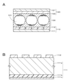
本技術の第2の実施形態に係るディスプレイは、フレキシブル性を有するマイクロカプセル電気泳動方式の電子ペーパーであり、図3Aに示すように、第1の導電性素子110と、第1の導電性素子110と対向配置された第2の導電性素子120と、これらの両素子間に設けられたマイクロカプセル層(媒質層)130とを備える。このディスプレイは、フレキシブルデバイスの一例である。ここでは、マイクロカプセル電気泳動方式の電子ペーパーに対して本技術を適用した例について説明するが、電子ペーパーはこの例に限定されるものではなく、ツイストボール方式、サーマルリライタブル方式、トナーディスプレイ方式、In-Plane型電気泳動方式または電子粉粒方式などの電子パーパーにも本技術は適用可能である。また、液晶ディスプレイまたは有機EL(Electro Luminescence)ディスプレイなどにも本技術は適用可能である。<2 Second Embodiment>
[2.1 Display configuration]
The display according to the second embodiment of the present technology is a flexible microcapsule electrophoresis type electronic paper, and as shown in FIG. 3A, the first
(マイクロカプセル層)
マイクロカプセル層130は、多数のマイクロカプセル131を含んでいる。マイクロカプセル131内には、例えば、黒色粒子おび白色粒子が分散された透明な液体(分散媒)が封入されている。(Microcapsule layer)
The
(第1、第2の導電性素子)
第1の導電性素子110は、積層体111と、積層体111の一方の面上に設けられた電極112とを備える。第2の導電性素子120は、積層体121と、積層体121の一方の面上に設けられた電極122とを備える。第1、第2の導電性素子110、120は、電極112、122が対向するように所定の間隔離して配置されている。(1st and 2nd conductive elements)
The first
電極112、122は、ディスプレイの駆動方式に応じて所定の電極パターン状に形成されている。駆動方式としては、例えば単純マトリックス駆動方式、アクティブマトリックス駆動方式、セグメント駆動方式などが挙げられる。
The
積層体111は、図3Bに示すように、基体111aと、基体111aの他方の面上に設けられた強化層111bと、強化層111b上に設けられた湾曲抑制層111cとを備える。基体111a、強化層111bおよび湾曲抑制層111cは、可視光に対して透明性を有するものであってもよいし、不透明性を有するものであってもよい。
As shown in FIG. 3B, the
基体111aは、フィルム状を有する。ここで、フィルムには、シートも含まれるものとする。基体111aの厚さは、好ましくは10μm以下である。基体111aの厚さが10μm以下であると、強化層111bおよび湾曲抑制層111cを備えることで得られる効果が顕著であるからである。基体111aの材料としては、例えば、高分子樹脂を用いることができる。高分子樹脂としては、例えば、ポリエチレンテレフタレート(PET)、ポリエチレンナフタレート(PEN)、ポリカーボネート(PC)、アクリル樹脂(PMMA)、ポリイミド(PI)、トリアセチルセルロース(TAC)、ポリエステル、ポリアミド(PA)、アラミド、ポリエチレン(PE)、ポリアクリレート、ポリエーテルスルフォン、ポリスルフォン、ポリプロピレン(PP)、ジアセチルセルロース、ポリ塩化ビニル、エポキシ樹脂、尿素樹脂、ウレタン樹脂、メラミン樹脂、環状オレフィンポリマー(COP)およびノルボルネン系熱可塑性樹脂のうちの少なくとも1種を用いることができる。
The substrate 111a has a film shape. Here, it is assumed that the film also includes a sheet. The thickness of the substrate 111a is preferably 10 μm or less. This is because when the thickness of the substrate 111a is 10 μm or less, the effect obtained by providing the reinforcing
強化層111b、湾曲抑制層111cはそれぞれ、第1の実施形態における強化層14、カッピング抑制層15と同様である。
The reinforcing
湾曲抑制層111cが設けられた側における第1の導電性素子110の表面抵抗は、好ましくは0.4Ω/□以下である。ここで、表面抵抗は、4端子法にて測定された値である。
The surface resistance of the first
積層体111の湿度膨張係数が、好ましくは0.5ppm/%RH以上、4ppm/%RH以下である。湿度膨張係数が上記範囲であると、第1の導電性素子110の寸法安定性をさらに向上できる。
The humidity expansion coefficient of the
積層体121は、積層体111と同様の構成を有するので、説明を省略する。但し、積層体121に備えられる基体、強化層および湾曲抑制層としては、可視光に対して透明性を有するものが用いられる。
Since the
[2.2 効果]
第2の実施形態に係るディスプレイでは、電極112、122が対向するように配置されている第1、第2の導電性素子110、120を備える。第1の導電性素子110は、基体111aの他方の面に強化層111bおよび湾曲抑制層111cを備えるので、強化層11bと湾曲抑制層111cとの内部応力が相殺し合って、第1導電性素子に対する湾曲の発生を抑制できる。したがって、寸法安定性に優れ、かつ湾曲を抑制できる第1の導電性素子110が得られる。すなわち、第1の導電性素子110の形状安定性を向上できる。第2の導電性素子120も第1の導電性素子110と同様の構成を有するため、第2の導電性素子120の形状安定性を向上できる。よって、電極112、122を高集積化した場合であっても、電極112、122のパターン同士の重ね合わせ精度の劣化を抑制できるので、高品質のディスプレイの提供が可能となる。[2.2 Effect]
The display according to the second embodiment includes first and second
[2.3 変形例]
上述の第2の実施形態では、本技術をディスプレイおよびそれに備えられる第1、第2の導電性素子110、120に本技術を適用する例について説明したが、本技術はこれに限定されるものではない。例えば、電磁シールド、タッチパネル、各種のウェアラブルデバイスにも本技術は適用可能である。本技術をタッチパネルやウェアラブルデバイスに適用した場合には、例えば、高集積化された電極パターンや配線パターン同士の重ね合わせ精度の劣化を抑制することができる。[2.3 Modification example]
In the second embodiment described above, an example of applying the present technology to the display and the first and second
上述の第2の実施形態では、フレキシブルデバイス(フレキシブルディスプレイ)に本技術を適用する例について説明したが、本技術はフレキシブル性を有していないデバイスにも適用可能である。 In the second embodiment described above, an example of applying the present technology to a flexible device (flexible display) has been described, but the present technology can also be applied to a device having no flexibility.
積層体111が、基体111aの他方の面(電極112側とは反対側の面)に強化層111bおよび湾曲抑制層111cを備える代わりに、基体111aの一方の面(電極112側の面)に強化層111bおよび湾曲抑制層111cを備えるようにしてもよい。この場合、湾曲抑制層111cと電極112との間には絶縁層が設けられる。積層体121も、上記の積層体111と同様の構成としてもよい。
Instead of providing the reinforcing
積層体111が、基体11の両面に強化層14を備えるようにしてもよい。この場合、湾曲抑制層111cは、両面に備えられた強化層111bのうち内部応力がより大きいものの側に設けられる。積層体121も、上記の積層体111と同様の構成としてもよい。
The laminate 111 may be provided with reinforcing
以下、実施例により本技術を具体的に説明するが、本技術はこれらの実施例のみに限定されるものではない。 Hereinafter, the present technology will be specifically described with reference to Examples, but the present technology is not limited to these Examples.
なお、以下の実施例および比較例において、強化層およびカッピング抑制層の平均厚みは、第1の実施形態にて説明した方法と同様にして求めた。 In the following Examples and Comparative Examples, the average thickness of the reinforcing layer and the cupping suppressing layer was determined in the same manner as in the method described in the first embodiment.
本実施例について以下の順序で説明する。
i 磁気テープについての実施例、比較例
ii 電磁シールドについての実施例This embodiment will be described in the following order.
i Examples and comparative examples of magnetic tapes
ii Examples of electromagnetic shield
<i 磁気テープについての実施例、比較例>
[実施例1~14、34~39]
(記録層形成用塗料の調製工程)
まず、記録層形成用塗料を以下のようにして調製した。まず、下記原料をエクストルーダで混練して混練物を得た。
CoNiフェライト結晶磁性粉:100質量部
(形状:ほぼ立方体形状、平均板径:11nm、平均板状比:0.95)
塩化ビニル系樹脂(シクロヘキサノン溶液30質量%):55.6質量部
(重合度300、Mn=10000、極性基としてOSO3K=0.07mmol/g、2級OH=0.3mmol/gを含有する。)
酸化アルミニウム粉末:5質量部
(α-Al2O3、平均粒径0.2μm)
カーボンブラック:2質量部
(東海カーボン社製、商品名:シーストTA)<Examples and Comparative Examples of i Magnetic Tapes>
[Examples 1 to 14, 34 to 39]
(Preparation process of paint for forming recording layer)
First, a coating material for forming a recording layer was prepared as follows. First, the following raw materials were kneaded with an extruder to obtain a kneaded product.
CoNi ferrite crystal magnetic powder: 100 parts by mass (shape: almost cubic shape, average plate diameter: 11 nm, average plate shape ratio: 0.95)
Vinyl chloride resin (cyclohexanone solution 30% by mass): 55.6 parts by mass (polymerization degree 300 , Mn = 10000, OSO 3K = 0.07 mmol / g as polar group, secondary OH = 0.3 mmol / g do.)
Aluminum oxide powder: 5 parts by mass (α-Al 2 O 3 , average particle size 0.2 μm)
Carbon black: 2 parts by mass (manufactured by Tokai Carbon Co., Ltd., product name: Seast TA)
次に、ディスパーを備えた攪拌タンクに、混練物と、下記原料とを加えて予備混合を行った。その後、さらにサンドミル混合を行い、フィルター処理を行い、記録層形成用塗料を調製した。
塩化ビニル系樹脂:27.8質量部
(樹脂溶液:樹脂分30質量%、シクロヘキサノン70質量%)
ポリイソシアネート:4質量部
(商品名:コロネートL、日本ポリウレタン社製)
ミリスチン酸:2質量部
n-ブチルステアレート:2質量部
メチルエチルケトン:121.3質量部
トルエン:121.3質量部
シクロヘキサノン:60.7質量部Next, the kneaded product and the following raw materials were added to a stirring tank equipped with a disper and premixed. Then, sand mill mixing was further performed and filtering was performed to prepare a coating material for forming a recording layer.
Vinyl chloride resin: 27.8 parts by mass (resin solution: resin content 30% by mass, cyclohexanone 70% by mass)
Polyisocyanate: 4 parts by mass (trade name: Coronate L, manufactured by Nippon Polyurethane Industry Co., Ltd.)
Myristic acid: 2 parts by mass n-butyl stearate: 2 parts by mass Methyl ethyl ketone: 121.3 parts by mass Toluene: 121.3 parts by mass Cyclohexanone: 60.7 parts by mass
(下地層形成用塗料の調製工程)
次に、下地層形成用塗料を以下のようにして調製した。まず、下記原料をエクストルーダで混練して混練物を得た。
針状酸化鉄粉末:100質量部
(α-Fe2O3、平均長軸長0.15μm)
塩化ビニル系樹脂:55.6質量部
(樹脂溶液:樹脂分30質量%、シクロヘキサノン70質量%)
カーボンブラック:10質量部
(平均粒径20nm)(Preparation process of paint for forming the base layer)
Next, the paint for forming the base layer was prepared as follows. First, the following raw materials were kneaded with an extruder to obtain a kneaded product.
Needle-shaped iron oxide powder: 100 parts by mass (α-Fe 2 O 3 , average major axis length 0.15 μm)
Vinyl chloride resin: 55.6 parts by mass (resin solution: resin content 30% by mass, cyclohexanone 70% by mass)
Carbon black: 10 parts by mass (average particle size 20 nm)
次に、ディスパーを備えた攪拌タンクに、混練物と、下記原料とを加えて予備混合を行った。その後、さらにサンドミル混合を行い、フィルター処理を行い、下地層形成用塗料を調製した。
ポリウレタン系樹脂UR8200(東洋紡績製):18.5質量部
ポリイソシアネート:4質量部
(商品名:コロネートL、日本ポリウレタン社製)
ミリスチン酸:2質量部
n-ブチルステアレート:2質量部
メチルエチルケトン:108.2質量部
トルエン:108.2質量部
シクロヘキサノン:18.5質量部Next, the kneaded product and the following raw materials were added to a stirring tank equipped with a disper and premixed. After that, further sand mill mixing was performed and a filter treatment was performed to prepare a paint for forming a base layer.
Polyurethane resin UR8200 (manufactured by Toyobo): 18.5 parts by mass Polyisocyanate: 4 parts by mass (trade name: Coronate L, manufactured by Nippon Polyurethane Industry Co., Ltd.)
Myristic acid: 2 parts by mass n-butyl stearate: 2 parts by mass Methyl ethyl ketone: 108.2 parts by mass Toluene: 108.2 parts by mass Cyclohexanone: 18.5 parts by mass
(バック層形成用塗料の調製工程)
次に、バック層形成用塗料を以下のようにして調製した。下記原料を、ディスパーを備えた攪拌タンクで混合を行い、フィルター処理を行うことで、バック層形成用塗料を調製した。
カーボンブラック(旭社製、商品名:#80):100質量部
ポリエステルポリウレタン:100質量部
(日本ポリウレタン社製、商品名:N-2304)
メチルエチルケトン:500質量部
トルエン:400質量部
シクロヘキサノン:100質量部(Preparation process of paint for forming back layer)
Next, the paint for forming the back layer was prepared as follows. The following raw materials were mixed in a stirring tank equipped with a disper and filtered to prepare a paint for forming a back layer.
Carbon black (manufactured by Asahi Co., Ltd., product name: # 80): 100 parts by mass Polyester polyurethane: 100 parts by mass (manufactured by Nippon Polyurethane Industry Co., Ltd., product name: N-2304)
Methyl ethyl ketone: 500 parts by mass Toluene: 400 parts by mass Cyclohexanone: 100 parts by mass
(強化層の形成工程)
次に、Roll to Roll方式の真空蒸着装置を用いて、厚さ6.2μm、帯状のPENフィルム(基体)の一方の面上に単層のCu層(強化層)を形成した。この際、フィルム巻取り速度などの成膜条件を調整することで、表1、表3に示すようにCu層の平均厚みを設定した。(Strengthening layer forming process)
Next, a single Cu layer (reinforced layer) was formed on one surface of a strip-shaped PEN film (base) having a thickness of 6.2 μm using a roll-to-roll vacuum vapor deposition apparatus. At this time, the average thickness of the Cu layer was set as shown in Tables 1 and 3 by adjusting the film forming conditions such as the film winding speed.
(カッピング抑制層の形成工程)
次に、Roll to Roll方式のCVD装置を用いて、DLC層(カッピング抑制層)をCu層上に形成した。この際、フィルム巻取り速度、導入ガス流量および放電電圧などの成膜条件を調整することで表1、表3に示すようにDLC層の平均厚みを設定した。(Step of forming cupping suppression layer)
Next, a DLC layer (cupping suppression layer) was formed on the Cu layer using a Roll to Roll type CVD device. At this time, the average thickness of the DLC layer was set as shown in Tables 1 and 3 by adjusting the film forming conditions such as the film winding speed, the introduced gas flow rate, and the discharge voltage.
(下地層の形成工程)
次に、PENフィルムの他方の面上に下地層形成用塗料を塗布し、乾燥させることにより、PENフィルムの他方の面上に厚さ1μmの下地層を形成した。(Step of forming the base layer)
Next, a paint for forming a base layer was applied on the other surface of the PEN film and dried to form a base layer having a thickness of 1 μm on the other surface of the PEN film.
(記録層の形成工程)
次に、下地層上に記録層形成用塗料を塗布し、乾燥させることにより、下地層上に厚さ70nmの記録層を形成した。(Recording layer forming process)
Next, a recording layer forming paint was applied on the base layer and dried to form a recording layer having a thickness of 70 nm on the base layer.
(熱処理の工程)
次に、得られた幅広の磁気テープに熱処理を施した。熱処理の温度は、表1、表3に示すように調整した。(Heat treatment process)
Next, the obtained wide magnetic tape was heat-treated. The heat treatment temperature was adjusted as shown in Tables 1 and 3.
(バック層の形成工程)
次に、表面改質によりDLC層の表面の濡れ性を改善した後、DLC層上にバック層形成用塗料を塗布し、乾燥させることにより、DLC層上に厚さ0.6μmのバック層を形成した。これにより、幅広の磁気テープを得た。(Back layer forming process)
Next, after improving the wettability of the surface of the DLC layer by surface modification, a paint for forming a back layer is applied on the DLC layer and dried to form a back layer having a thickness of 0.6 μm on the DLC layer. Formed. This gave a wide magnetic tape.
(カレンダー処理および裁断の工程)
次に、磁気テープに対して、金属ロールによるカレンダー処理を行い、記録層表面を平滑化した。次に、幅広の磁気テープを1/2インチ(12.65mm)幅に裁断して、目的とする磁気テープを得た。(Calendar processing and cutting process)
Next, the magnetic tape was subjected to calendar processing with a metal roll to smooth the surface of the recording layer. Next, the wide magnetic tape was cut to a width of 1/2 inch (12.65 mm) to obtain the desired magnetic tape.
[実施例15~28、40、41]
強化層を2層構造にすること、Cu層およびDLC層の平均厚みが表1、表3に示す値となるようにCu層およびDLC層の成膜条件を調整したこと以外は実施例1と同様にして磁気テープを得た。[Examples 15 to 28, 40, 41]
Example 1 except that the reinforcing layer has a two-layer structure and the film forming conditions of the Cu layer and the DLC layer are adjusted so that the average thickness of the Cu layer and the DLC layer becomes the values shown in Tables 1 and 3. A magnetic tape was obtained in the same manner.
[実施例29]
強化層として単層のCu層に代えて単層のAl層を形成する以外は実施例11と同様にして磁気テープを得た。[Example 29]
A magnetic tape was obtained in the same manner as in Example 11 except that a single Al layer was formed instead of the single Cu layer as the reinforcing layer.
[実施例30]
強化層として単層のCu層に代えて2層のAl層を形成する以外は実施例25と同様にして磁気テープを得た。[Example 30]
A magnetic tape was obtained in the same manner as in Example 25 except that a two-layer Al layer was formed instead of the single-layer Cu layer as the reinforcing layer.
[実施例31]
強化層としてCu層に代えてSiO2層を形成する以外は実施例11と同様にして磁気テープを得た。[Example 31]
A magnetic tape was obtained in the same manner as in Example 11 except that a SiO 2 layer was formed instead of the Cu layer as the reinforcing layer.
[実施例32]
蒸着の際、酸素を導入することでCuO層を形成する以外は、実施例11と同様にして磁気テープを得た。[Example 32]
A magnetic tape was obtained in the same manner as in Example 11 except that a CuO layer was formed by introducing oxygen during the vapor deposition.
[実施例33]
蒸着の際、酸素を導入することでAl2O3層を形成する以外は、実施例29と同様にして磁気テープを得た。[Example 33]
A magnetic tape was obtained in the same manner as in Example 29, except that an Al 2 O 3 layer was formed by introducing oxygen during the vapor deposition.
[実施例42]
磁気テープに対する熱処理の工程を省く以外のことは実施例1と同様にして磁気テープを得た。[Example 42]
A magnetic tape was obtained in the same manner as in Example 1 except that the step of heat-treating the magnetic tape was omitted.
[比較例1]
DLC層の形成を省略すること以外は実施例3と同様にして磁気テープを得た。[Comparative Example 1]
A magnetic tape was obtained in the same manner as in Example 3 except that the formation of the DLC layer was omitted.
[評価]
上述のようにして得られた実施例1~42、比較例1の磁気テープについて以下の評価を行った。[evaluation]
The magnetic tapes of Examples 1 to 42 and Comparative Example 1 obtained as described above were evaluated as follows.
(ヤング率)
まず、温度23℃、相対湿度60%の環境下において、引っ張り試験機(MNB社製 TCM-200CR)を用いて磁気テープのヤング率を測定した。(Young's modulus)
First, the Young's modulus of the magnetic tape was measured using a tensile tester (TCM-200CR manufactured by MNB) in an environment of a temperature of 23 ° C. and a relative humidity of 60%.
(蒸着膜付着強度)
LTO規格 Ultrium Generation6 Specification Document U-616 Section 9.8.1の方法に従い蒸着膜(強化層)の付着強度を測定した。次に、その測定結果に基づき、以下の基準で判定した。
○:剥がれの発生がない
×:剥がれの発生がある(Embedded film adhesion strength)
The adhesion strength of the vapor deposition film (reinforced layer) was measured according to the method of LTO standard Ultrium Generation6 Specification Document U-616 Section 9.8.1. Next, based on the measurement result, the judgment was made according to the following criteria.
◯: No peeling occurred ×: Peeling occurred
(湿度膨張係数)
恒温槽を環境条件1(温度16℃、相対湿度10%)から環境条件2(温度29℃、相対湿度80%)まで変化させた場合の寸法変化を、キーエンス社製レーザー変位計LS-7000を用いて測定した。次に、以下の式により湿度膨張係数を求めた。
TDS(湿度)[ppm]=((温度29℃、相対湿度80%のテープ幅)-(温度16℃、相対湿度10%のテープ幅))/(温度16℃、相対湿度10%のテープ幅)
湿度膨張係数[ppm/%RH]=TDS(湿度)/(80-10)(Humidity expansion coefficient)
Keyence's laser displacement meter LS-7000 can be used to measure the dimensional changes when the constant temperature bath is changed from environmental condition 1 (
TDS (humidity) [ppm] = ((Temperature 29 ° C, relative humidity 80% tape width)-(
Humidity expansion coefficient [ppm /% RH] = TDS (humidity) / (80-10)
(カッピング)
カッピング測定装置を用い、温度23℃、相対湿度60%の環境下において、スリット後のテープ1mを24時間放置した後、カッピングの量を測定した。記録層を上側にして記録層側が凸になるカッピングをマイナス(-)、バック層側が凸になるカッピングをプラス(+)として、カッピングの量を測定し、以下の基準で判定した。
◎:カッピング量が0.0~-0.5mmの範囲内
○:カッピング量が-0.5~-1.0mmの範囲内
△:カッピング量が-1.0~-1.5mmの範囲内
×:カッピング量が0.0~-1.5mmの範囲外
なお、測定サンプル長は1±0.1mとする。(Cupping)
Using a coupling measuring device, the amount of coupling was measured after leaving 1 m of the tape after slitting for 24 hours in an environment of a temperature of 23 ° C. and a relative humidity of 60%. The amount of cupping was measured with the cupping with the recording layer on the upper side and the cupping with the recording layer side convex as minus (−) and the cupping with the back layer side as plus (+), and determined according to the following criteria.
⊚: Capping amount is within the range of 0.0 to -0.5 mm ○: Capping amount is within the range of -0.5 to -1.0 mm Δ: Capping amount is within the range of -1.0 to -1.5 mm X: The cupping amount is out of the range of 0.0 to −1.5 mm. The measurement sample length is 1 ± 0.1 m.
(テープ走行摩擦上昇)
1/2インチ固定ヘッド型ドライブ(LTO5)を用いて、一定区間(10m長)の100000回走行を行い、以下の基準で判定した。
○:リファレンステープ(MSRT)と同等の摩擦で走行が継続する
△:走行は継続するがリファレンステープ(MSRT)よりも摩擦が高い
×:走行がストップする(Rising tape running friction)
Using a 1/2 inch fixed head type drive (LTO5), 100,000 times of running in a certain section (10 m length) were performed, and the judgment was made according to the following criteria.
○: Running continues with the same friction as the reference tape (MSRT) △: Running continues but the friction is higher than the reference tape (MSRT) ×: Running stops
(SNR)
まず、市販のMountain Engineering社製のテープ走行系にて磁気テープを走行させ、1/2インチ固定ヘッド型ドライブの磁気ヘッドを用いて記録再生を行うことにより、SNRを求めた。次に、求めたSNRを以下の基準で判定した。
○:SNRがLTO5メディアのリファレンステープ(MSRT)に対して-1.5dB以内となる
△:SNRがLTO5メディアのリファレンステープ(MSRT)に対して-1.5dBを超え、-2.5dB以内となる
×:SNRがLTO5メディアのリファレンステープ(MSRT)に対して-2.5dBを超える(SNR)
First, the SNR was obtained by running a magnetic tape on a commercially available tape running system manufactured by Mountain Engineering and performing recording and reproduction using a magnetic head of a 1/2 inch fixed head type drive. Next, the obtained SNR was determined according to the following criteria.
◯: SNR is within -1.5 dB with respect to the reference tape (MSRT) of LTO5 media Δ: SNR is more than -1.5 dB and within -2.5 dB with respect to the reference tape (MSRT) of LTO5 media. X: SNR exceeds -2.5 dB with respect to the reference tape (MSRT) of LTO5 media.
(結果)
表1、表2は、実施例1~28の磁気テープの構成および評価結果を示す。

Tables 1 and 2 show the configurations and evaluation results of the magnetic tapes of Examples 1 to 28.

表3、表4は、実施例29~42、比較例1の磁気テープの構成および評価結果を示す。


表1~表4から以下のことがわかる。
金属層または金属酸化物層上にDLC層を設けることで、磁気テープのカッピングを抑制できる。
金属層または金属酸化物層の平均厚みを150nm以上500nm以下の範囲内とすることで、湿度膨張係数を0.5ppm/%RH以上、4ppm/%RH以下の範囲内とすることができる。したがって、磁気テープの寸法安定性をより向上できる。
金属層または金属酸化物層の平均厚みを150nm以上500nm以下の範囲内とし、かつ、金属層または金属酸化物層の平均厚みに対するDLC層の平均厚みの比率を0.05以上0.7以下とすることで、磁気テープのカッピングをさらに抑制できる。
熱処理の工程を備えず、カッピング抑制層を設けるのみでも磁気テープのカッピングを十分に抑制できる。The following can be seen from Tables 1 to 4.
By providing the DLC layer on the metal layer or the metal oxide layer, cupping of the magnetic tape can be suppressed.
By setting the average thickness of the metal layer or the metal oxide layer within the range of 150 nm or more and 500 nm or less, the humidity expansion coefficient can be set within the range of 0.5 ppm /% RH or more and 4 ppm /% RH or less. Therefore, the dimensional stability of the magnetic tape can be further improved.
The average thickness of the metal layer or metal oxide layer should be within the range of 150 nm or more and 500 nm or less, and the ratio of the average thickness of the DLC layer to the average thickness of the metal layer or metal oxide layer should be 0.05 or more and 0.7 or less. By doing so, the coupling of the magnetic tape can be further suppressed.
The cupping of the magnetic tape can be sufficiently suppressed only by providing the cupping suppressing layer without the heat treatment step.
<ii 電磁シールドについての実施例>
[実施例43]
Cu層およびDLC層の平均厚みが表5に示す値となるようにCu層およびDLC層の成膜条件を調整したこと以外は実施例1と同様にして、厚さ6.2μm、帯状のPENフィルム(基体)上にCu層およびDLC層を積層した。これにより、目的とする電磁シールドが得られた。<Ii Example of electromagnetic shield>
[Example 43]
Similar to Example 1, except that the film forming conditions of the Cu layer and the DLC layer were adjusted so that the average thickness of the Cu layer and the DLC layer became the values shown in Table 5, the thickness was 6.2 μm and the strip-shaped PEN was formed. A Cu layer and a DLC layer were laminated on the film (base). As a result, the desired electromagnetic shield was obtained.
[実施例44]
CuO層およびDLC層の平均厚みが表5に示す値となるようにCuO層およびDLC層の成膜条件を調整したこと以外は実施例32と同様にして、厚さ6.2μm、帯状のPENフィルム(基体)上にCuO層およびDLC層を積層した。これにより、目的とする電磁シールドが得られた。[Example 44]
Similar to Example 32, a strip-shaped PEN having a thickness of 6.2 μm, except that the film forming conditions of the CuO layer and the DLC layer were adjusted so that the average thickness of the CuO layer and the DLC layer became the values shown in Table 5. A CuO layer and a DLC layer were laminated on the film (base). As a result, the desired electromagnetic shield was obtained.
[評価]
上述のようにして得られた実施例43、44の磁気シールドについて、ヤング率、湿度膨張係数、カッピングおよび電磁波透過率を評価した。なお、ヤング率、湿度膨張係数およびカッピングの評価方法は、上述の実施例1~42におけるのと同様のものとした。[evaluation]
Young's modulus, humidity expansion coefficient, cupping and electromagnetic wave transmittance were evaluated for the magnetic shields of Examples 43 and 44 obtained as described above. The Young's modulus, the humidity expansion coefficient, and the cupping evaluation method were the same as those in Examples 1 to 42 described above.
(電磁波透過率)
磁気シールドの電磁波透過率をアドバンテスト法により測定した。(Electromagnetic wave transmittance)
The electromagnetic wave transmittance of the magnetic shield was measured by the Advantest method.
表5、表6は、実施例43、44の積層体の構成および評価結果を示す。


表5、表6から以下のことがわかる。
金属層または金属酸化物層上にDLC層を設けることで、電磁シールドの湾曲を抑制できる。したがって、平面性に優れた電磁シールドが得られる。The following can be seen from Tables 5 and 6.
By providing the DLC layer on the metal layer or the metal oxide layer, the bending of the electromagnetic shield can be suppressed. Therefore, an electromagnetic shield having excellent flatness can be obtained.
以上、本技術の実施形態および実施例について具体的に説明したが、本技術は、上述の実施形態および実施例に限定されるものではなく、本技術の技術的思想に基づく各種の変形が可能である。 Although the embodiments and examples of the present technology have been specifically described above, the present technology is not limited to the above-mentioned embodiments and examples, and various modifications based on the technical idea of the present technology are possible. Is.
例えば、上述の実施形態および実施例において挙げた構成、方法、工程、形状、材料および数値などはあくまでも例に過ぎず、必要に応じてこれと異なる構成、方法、工程、形状、材料および数値などを用いてもよい。 For example, the configurations, methods, processes, shapes, materials, numerical values, etc. given in the above-described embodiments and examples are merely examples, and different configurations, methods, processes, shapes, materials, numerical values, etc., if necessary, etc. May be used.
また、上述の実施形態および実施例の構成、方法、工程、形状、材料および数値などは、本技術の主旨を逸脱しない限り、互いに組み合わせることが可能である。 In addition, the configurations, methods, processes, shapes, materials, numerical values, and the like of the above-described embodiments and examples can be combined with each other as long as they do not deviate from the gist of the present technology.
また、本技術は以下の構成を採用することもできる。
(1)
長尺状の基体と、
前記基体の一方の面上に設けられた強化層およびカッピング抑制層と
を備える磁気記録媒体。
(2)
前記カッピング抑制層は、炭素薄膜である(1)に記載の磁気記録媒体。
(3)
前記炭素薄膜は、ダイヤモンドライクカーボンを含む(2)に記載の磁気記録媒体。
(4)
前記強化層は、金属および金属化合物のうちの少なくとも1種を含む(1)から(3)のいずれかに記載の磁気記録媒体。
(5)
前記金属化合物は、金属酸化物である(4)に記載の磁気記録媒体。
(6)
前記金属は、アルミニウムおよび銅のうちの少なくとも1種を含み、
前記金属化合物は、酸化アルミニウム、酸化銅および酸化シリコンのうちの少なくとも1種を含む(4)に記載の磁気記録媒体。
(7)
前記強化層は、内部応力として引っ張り応力が働くものであり、
前記カッピング抑制層は、内部応力として圧縮応力が働くものである(1)から(6)のいずれかに記載の磁気記録媒体。
(8)
前記強化層が、2層以上の積層構造を有する(1)から(7)のいずれかに記載の磁気記録媒体。
(9)
前記強化層が、
第1の金属酸化物層と、
第2の金属酸化物層と、
前記第1金属酸化物層および前記第2金属酸化物層の間に設けられた金属層と
を備える(1)から(8)のいずれかに記載の磁気記録媒体。
(10)
前記強化層が、金属および酸素を含み、
前記強化層の両面のうち、前記基体とは反対側の面における酸素濃度が、前記強化層の内部における酸素濃度に比して高い(1)から(7)のいずれかに記載の磁気記録媒体。
(11)
前記強化層の両面における酸素濃度が、前記強化層の内部における酸素濃度に比して高い(10)に記載の磁気記録媒体。
(12)
前記カッピング抑制層が、2層以上の積層構造を有する(1)から(11)のいずれかに記載の磁気記録媒体。
(13)
前記強化層が、前記基体上に設けられ、
前記カッピング抑制層が、前記強化層上に設けられている(1)から(12)のいずれかに記載の磁気記録媒体。
(14)
前記強化層の平均厚みが、150nm以上500nm以下であり、
前記強化層の平均厚みに対する前記カッピング抑制層の平均厚みの比率が、0.05以上0.7以下である(1)から(13)のいずれかに記載の磁気記録媒体。
(15)
長手方向のヤング率が、7GPa以上14GPa以下である(1)から(14)のいずれかに記載の磁気記録媒体。
(16)
前記基体の他方の面上に設けられた非磁性層と、
前記非磁性層上に設けられた磁性層と
前記カッピング抑制層上に設けられたバック層と
をさらに備える(1)から(15)のいずれかに記載の磁気記録媒体。
(17)
長尺状の基体と、
前記基体の一方の面上に設けられた強化層および炭素薄膜と
を備える磁気記録媒体。
(18)
基体と、
前記基体の一方の面上に設けられた強化層およびカッピング抑制層と
を備える積層体。
(19)
前記基体の厚みは、10μm以下である(18)に記載の積層体。
(20)
前記カッピング抑制層が設けられた側の表面抵抗が、0.4Ω/□以下である(18)または(19)に記載の積層体。
(21)
湿度膨張係数が、0.5ppm/%RH以上、4ppm/%RH以下である(18)から(20)のいずれかに記載の積層体。
(22)
基体と、
前記基体の一方の面上に設けられた強化層および炭素薄膜と
を備える積層体。
(23)
(18)から(22)のいずれかに記載の積層体を備えるフレキシブルデバイス。In addition, the present technology can also adopt the following configurations.
(1)
With a long substrate,
A magnetic recording medium including a reinforcing layer and a cupping suppressing layer provided on one surface of the substrate.
(2)
The magnetic recording medium according to (1), wherein the cupping suppression layer is a carbon thin film.
(3)
The magnetic recording medium according to (2), wherein the carbon thin film contains diamond-like carbon.
(4)
The magnetic recording medium according to any one of (1) to (3), wherein the reinforcing layer contains at least one of a metal and a metal compound.
(5)
The magnetic recording medium according to (4), wherein the metal compound is a metal oxide.
(6)
The metal comprises at least one of aluminum and copper.
The magnetic recording medium according to (4), wherein the metal compound contains at least one of aluminum oxide, copper oxide and silicon oxide.
(7)
The reinforcing layer has a tensile stress acting as an internal stress.
The magnetic recording medium according to any one of (1) to (6), wherein the cupping suppressing layer has a compressive stress acting as an internal stress.
(8)
The magnetic recording medium according to any one of (1) to (7), wherein the reinforcing layer has a laminated structure of two or more layers.
(9)
The reinforcing layer is
The first metal oxide layer and
The second metal oxide layer and
The magnetic recording medium according to any one of (1) to (8), comprising the first metal oxide layer and a metal layer provided between the second metal oxide layers.
(10)
The reinforcing layer contains metal and oxygen and contains
The magnetic recording medium according to any one of (1) to (7), wherein the oxygen concentration on the surface of both sides of the reinforcing layer opposite to the substrate is higher than the oxygen concentration inside the reinforcing layer. ..
(11)
The magnetic recording medium according to (10), wherein the oxygen concentration on both sides of the reinforcing layer is higher than the oxygen concentration inside the reinforcing layer.
(12)
The magnetic recording medium according to any one of (1) to (11), wherein the cupping suppression layer has a laminated structure of two or more layers.
(13)
The reinforcing layer is provided on the substrate, and the reinforcing layer is provided on the substrate.
The magnetic recording medium according to any one of (1) to (12), wherein the cupping suppression layer is provided on the reinforcing layer.
(14)
The average thickness of the reinforcing layer is 150 nm or more and 500 nm or less.
The magnetic recording medium according to any one of (1) to (13), wherein the ratio of the average thickness of the cupping suppressing layer to the average thickness of the reinforcing layer is 0.05 or more and 0.7 or less.
(15)
The magnetic recording medium according to any one of (1) to (14), wherein the Young's modulus in the longitudinal direction is 7 GPa or more and 14 GPa or less.
(16)
A non-magnetic layer provided on the other surface of the substrate and
The magnetic recording medium according to any one of (1) to (15), further comprising a magnetic layer provided on the non-magnetic layer and a back layer provided on the cupping suppression layer.
(17)
With a long substrate,
A magnetic recording medium including a reinforcing layer and a carbon thin film provided on one surface of the substrate.
(18)
With the substrate
A laminated body including a reinforcing layer and a cupping suppressing layer provided on one surface of the substrate.
(19)
The laminate according to (18), wherein the thickness of the substrate is 10 μm or less.
(20)
The laminate according to (18) or (19), wherein the surface resistance on the side provided with the cupping suppression layer is 0.4 Ω / □ or less.
(21)
The laminate according to any one of (18) to (20), wherein the humidity expansion coefficient is 0.5 ppm /% RH or more and 4 ppm /% RH or less.
(22)
With the substrate
A laminate comprising a reinforcing layer and a carbon thin film provided on one surface of the substrate.
(23)
A flexible device comprising the laminate according to any one of (18) to (22).
10、111、121 積層体
11、111a 基体
12 下地層
13 記録層
14、121b 強化層
15、121c カッピング抑制層
16 バック層
110 第1の導電性素子
112、122 電極
120 第2の導電性素子
130 マイクロカプセル層
131 マイクロカプセル10, 111, 121
Claims (14)
前記基体の一方の面上に設けられた強化層およびカッピング抑制層と
を備え、
前記強化層が、
第1の金属酸化物層と、
第2の金属酸化物層と、
前記第1の金属酸化物層および前記第2の金属酸化物層の間に設けられた金属層と
を備える磁気記録媒体。 With a long substrate,
A reinforcing layer and a cupping suppressing layer provided on one surface of the substrate are provided .
The reinforcing layer is
The first metal oxide layer and
The second metal oxide layer and
With the metal layer provided between the first metal oxide layer and the second metal oxide layer
A magnetic recording medium comprising .
前記カッピング抑制層は、内部応力として圧縮応力が働くものである請求項1から3のいずれかに記載の磁気記録媒体。 The reinforcing layer has a tensile stress acting as an internal stress.
The magnetic recording medium according to any one of claims 1 to 3 , wherein the cupping suppression layer is such that a compressive stress acts as an internal stress.
前記カッピング抑制層が、前記強化層上に設けられている請求項1から5のいずれかに記載の磁気記録媒体。 The reinforcing layer is provided on the substrate, and the reinforcing layer is provided on the substrate.
The magnetic recording medium according to any one of claims 1 to 5 , wherein the cupping suppressing layer is provided on the reinforcing layer.
前記強化層の平均厚みに対する前記カッピング抑制層の平均厚みの比率が、0.05以上0.7以下である請求項1から6のいずれかに記載の磁気記録媒体。 The average thickness of the reinforcing layer is 150 nm or more and 500 nm or less.
The magnetic recording medium according to any one of claims 1 to 6 , wherein the ratio of the average thickness of the cupping suppressing layer to the average thickness of the reinforcing layer is 0.05 or more and 0.7 or less.
前記非磁性層上に設けられた磁性層と
前記カッピング抑制層上に設けられたバック層と
をさらに備える請求項1から8のいずれかに記載の磁気記録媒体。 A non-magnetic layer provided on the other surface of the substrate and
The magnetic recording medium according to any one of claims 1 to 8 , further comprising a magnetic layer provided on the non-magnetic layer and a back layer provided on the cupping suppression layer.
前記基体の一方の面上に設けられた強化層およびカッピング抑制層と
を備え、
前記強化層が、
第1の金属酸化物層と、
第2の金属酸化物層と、
前記第1の金属酸化物層および前記第2の金属酸化物層の間に設けられた金属層と
を備える積層体。 With the substrate
A reinforcing layer and a cupping suppressing layer provided on one surface of the substrate are provided .
The reinforcing layer is
The first metal oxide layer and
The second metal oxide layer and
With the metal layer provided between the first metal oxide layer and the second metal oxide layer
A laminate comprising .
Applications Claiming Priority (3)
| Application Number | Priority Date | Filing Date | Title |
|---|---|---|---|
| JP2016095333 | 2016-05-11 | ||
| JP2016095333 | 2016-05-11 | ||
| PCT/JP2017/017885 WO2017195865A1 (en) | 2016-05-11 | 2017-05-11 | Magnetic recording medium, laminated body, and flexible device |
Publications (2)
| Publication Number | Publication Date |
|---|---|
| JPWO2017195865A1 JPWO2017195865A1 (en) | 2019-03-07 |
| JP7028162B2 true JP7028162B2 (en) | 2022-03-02 |
Family
ID=60267116
Family Applications (1)
| Application Number | Title | Priority Date | Filing Date |
|---|---|---|---|
| JP2018517077A Active JP7028162B2 (en) | 2016-05-11 | 2017-05-11 | Magnetic recording media, laminates and flexible devices |
Country Status (4)
| Country | Link |
|---|---|
| US (1) | US20200321025A1 (en) |
| JP (1) | JP7028162B2 (en) |
| DE (1) | DE112017002425T5 (en) |
| WO (1) | WO2017195865A1 (en) |
Families Citing this family (1)
| Publication number | Priority date | Publication date | Assignee | Title |
|---|---|---|---|---|
| WO2019187323A1 (en) * | 2018-03-30 | 2019-10-03 | ソニー株式会社 | Magnetic recording medium |
Citations (6)
| Publication number | Priority date | Publication date | Assignee | Title |
|---|---|---|---|---|
| JP2000195035A (en) | 1998-12-25 | 2000-07-14 | Matsushita Electric Ind Co Ltd | Magnetic recording medium and method of manufacturing the same |
| JP2005129157A (en) | 2003-10-23 | 2005-05-19 | Sony Corp | Magnetic recording medium, its manufacturing method and manufacturing device |
| JP2006221782A (en) | 2005-01-13 | 2006-08-24 | Sony Corp | Magnetic recording medium |
| JP2006302333A (en) | 2005-04-15 | 2006-11-02 | Matsushita Electric Ind Co Ltd | Magnetic recording medium |
| JP2008270784A (en) | 2007-03-26 | 2008-11-06 | Semiconductor Energy Lab Co Ltd | Semiconductor device and method for manufacturing same |
| JP2010052416A (en) | 2008-07-29 | 2010-03-11 | Toray Ind Inc | Laminated body, support for magnetic recording medium, and magnetic recording medium |
Family Cites Families (8)
| Publication number | Priority date | Publication date | Assignee | Title |
|---|---|---|---|---|
| JPS6113433A (en) | 1984-06-29 | 1986-01-21 | Fuji Photo Film Co Ltd | Magnetic recording medium |
| JPH11339250A (en) | 1998-05-25 | 1999-12-10 | Toray Ind Inc | Magnetic recording medium |
| JP2000011364A (en) | 1998-06-24 | 2000-01-14 | Toray Ind Inc | Magnetic recording medium |
| JP2002100027A (en) * | 2000-09-26 | 2002-04-05 | Sony Corp | Metallic thin film type magnetic recording medium |
| JP2002304721A (en) | 2001-04-09 | 2002-10-18 | Sony Corp | Magnetic recording medium |
| JP2002304720A (en) | 2001-04-09 | 2002-10-18 | Sony Corp | Magnetic recording medium |
| JP2003132525A (en) | 2001-10-29 | 2003-05-09 | Sony Corp | Magnetic recording medium |
| JP2011070714A (en) * | 2009-09-24 | 2011-04-07 | Teijin Dupont Films Japan Ltd | Support for magnetic recording medium and magnetic recording medium |
-
2017
- 2017-05-11 WO PCT/JP2017/017885 patent/WO2017195865A1/en active Application Filing
- 2017-05-11 DE DE112017002425.0T patent/DE112017002425T5/en not_active Withdrawn
- 2017-05-11 JP JP2018517077A patent/JP7028162B2/en active Active
- 2017-05-11 US US16/099,298 patent/US20200321025A1/en not_active Abandoned
Patent Citations (6)
| Publication number | Priority date | Publication date | Assignee | Title |
|---|---|---|---|---|
| JP2000195035A (en) | 1998-12-25 | 2000-07-14 | Matsushita Electric Ind Co Ltd | Magnetic recording medium and method of manufacturing the same |
| JP2005129157A (en) | 2003-10-23 | 2005-05-19 | Sony Corp | Magnetic recording medium, its manufacturing method and manufacturing device |
| JP2006221782A (en) | 2005-01-13 | 2006-08-24 | Sony Corp | Magnetic recording medium |
| JP2006302333A (en) | 2005-04-15 | 2006-11-02 | Matsushita Electric Ind Co Ltd | Magnetic recording medium |
| JP2008270784A (en) | 2007-03-26 | 2008-11-06 | Semiconductor Energy Lab Co Ltd | Semiconductor device and method for manufacturing same |
| JP2010052416A (en) | 2008-07-29 | 2010-03-11 | Toray Ind Inc | Laminated body, support for magnetic recording medium, and magnetic recording medium |
Also Published As
| Publication number | Publication date |
|---|---|
| WO2017195865A1 (en) | 2017-11-16 |
| JPWO2017195865A1 (en) | 2019-03-07 |
| DE112017002425T5 (en) | 2019-01-31 |
| US20200321025A1 (en) | 2020-10-08 |
Similar Documents
| Publication | Publication Date | Title |
|---|---|---|
| JP7031579B2 (en) | Magnetic recording medium | |
| JP7200986B2 (en) | Magnetic recording tape, manufacturing method thereof, magnetic recording tape cartridge | |
| JP7136273B2 (en) | magnetic recording medium | |
| JP7173005B2 (en) | magnetic recording medium | |
| US7014927B2 (en) | Magnetic recording medium | |
| JP7247953B2 (en) | Magnetic recording media and cartridges | |
| WO2021033332A1 (en) | Magnetic recording medium, magnetic recording and reproducing device, and magnetic recording medium cartridge | |
| JP2023082110A (en) | Data reproduction device | |
| JP7028162B2 (en) | Magnetic recording media, laminates and flexible devices | |
| WO2016157681A1 (en) | Magnetic recording medium | |
| JP2006073047A (en) | Method for manufacturing magnetic recording medium and magnetic recording medium | |
| JP2008059664A (en) | Magnetic recording medium | |
| JP2006286098A (en) | Magnetic recording medium and manufacturing method therefor | |
| JP2006302333A (en) | Magnetic recording medium | |
| JP2002074643A (en) | Magnetic recording medium | |
| JP2005353190A (en) | Magnetic recording medium | |
| JPH1011736A (en) | Magnetic tape for recording computer data | |
| JP2001307316A (en) | Magnetic recording medium | |
| JP2006281672A (en) | Heat-treating method of film and film | |
| JP2000155931A (en) | Magnetic recording medium |
Legal Events
| Date | Code | Title | Description |
|---|---|---|---|
| A521 | Request for written amendment filed |
Free format text: JAPANESE INTERMEDIATE CODE: A523 Effective date: 20200406 |
|
| A621 | Written request for application examination |
Free format text: JAPANESE INTERMEDIATE CODE: A621 Effective date: 20200406 |
|
| A131 | Notification of reasons for refusal |
Free format text: JAPANESE INTERMEDIATE CODE: A131 Effective date: 20210629 |
|
| A521 | Request for written amendment filed |
Free format text: JAPANESE INTERMEDIATE CODE: A523 Effective date: 20210824 |
|
| TRDD | Decision of grant or rejection written | ||
| A01 | Written decision to grant a patent or to grant a registration (utility model) |
Free format text: JAPANESE INTERMEDIATE CODE: A01 Effective date: 20220118 |
|
| A61 | First payment of annual fees (during grant procedure) |
Free format text: JAPANESE INTERMEDIATE CODE: A61 Effective date: 20220131 |
|
| R151 | Written notification of patent or utility model registration |
Ref document number: 7028162 Country of ref document: JP Free format text: JAPANESE INTERMEDIATE CODE: R151 |