JP7015472B2 - Image forming device, developing device and image forming unit - Google Patents
Image forming device, developing device and image forming unit Download PDFInfo
- Publication number
- JP7015472B2 JP7015472B2 JP2018028766A JP2018028766A JP7015472B2 JP 7015472 B2 JP7015472 B2 JP 7015472B2 JP 2018028766 A JP2018028766 A JP 2018028766A JP 2018028766 A JP2018028766 A JP 2018028766A JP 7015472 B2 JP7015472 B2 JP 7015472B2
- Authority
- JP
- Japan
- Prior art keywords
- developing
- sleeve
- image
- latent image
- image forming
- Prior art date
- Legal status (The legal status is an assumption and is not a legal conclusion. Google has not performed a legal analysis and makes no representation as to the accuracy of the status listed.)
- Active
Links
Images


Classifications
-
- G—PHYSICS
- G03—PHOTOGRAPHY; CINEMATOGRAPHY; ANALOGOUS TECHNIQUES USING WAVES OTHER THAN OPTICAL WAVES; ELECTROGRAPHY; HOLOGRAPHY
- G03G—ELECTROGRAPHY; ELECTROPHOTOGRAPHY; MAGNETOGRAPHY
- G03G15/00—Apparatus for electrographic processes using a charge pattern
- G03G15/50—Machine control of apparatus for electrographic processes using a charge pattern, e.g. regulating differents parts of the machine, multimode copiers, microprocessor control
- G03G15/5054—Machine control of apparatus for electrographic processes using a charge pattern, e.g. regulating differents parts of the machine, multimode copiers, microprocessor control by measuring the characteristics of an intermediate image carrying member or the characteristics of an image on an intermediate image carrying member, e.g. intermediate transfer belt or drum, conveyor belt
- G03G15/5058—Machine control of apparatus for electrographic processes using a charge pattern, e.g. regulating differents parts of the machine, multimode copiers, microprocessor control by measuring the characteristics of an intermediate image carrying member or the characteristics of an image on an intermediate image carrying member, e.g. intermediate transfer belt or drum, conveyor belt using a test patch
-
- G—PHYSICS
- G03—PHOTOGRAPHY; CINEMATOGRAPHY; ANALOGOUS TECHNIQUES USING WAVES OTHER THAN OPTICAL WAVES; ELECTROGRAPHY; HOLOGRAPHY
- G03G—ELECTROGRAPHY; ELECTROPHOTOGRAPHY; MAGNETOGRAPHY
- G03G15/00—Apparatus for electrographic processes using a charge pattern
- G03G15/06—Apparatus for electrographic processes using a charge pattern for developing
- G03G15/065—Arrangements for controlling the potential of the developing electrode
-
- G—PHYSICS
- G03—PHOTOGRAPHY; CINEMATOGRAPHY; ANALOGOUS TECHNIQUES USING WAVES OTHER THAN OPTICAL WAVES; ELECTROGRAPHY; HOLOGRAPHY
- G03G—ELECTROGRAPHY; ELECTROPHOTOGRAPHY; MAGNETOGRAPHY
- G03G15/00—Apparatus for electrographic processes using a charge pattern
- G03G15/01—Apparatus for electrographic processes using a charge pattern for producing multicoloured copies
- G03G15/0142—Structure of complete machines
- G03G15/0147—Structure of complete machines using a single reusable electrographic recording member
- G03G15/0152—Structure of complete machines using a single reusable electrographic recording member onto which the monocolour toner images are superposed before common transfer from the recording member
- G03G15/0173—Structure of complete machines using a single reusable electrographic recording member onto which the monocolour toner images are superposed before common transfer from the recording member plural rotations of recording member to produce multicoloured copy, e.g. rotating set of developing units
-
- G—PHYSICS
- G03—PHOTOGRAPHY; CINEMATOGRAPHY; ANALOGOUS TECHNIQUES USING WAVES OTHER THAN OPTICAL WAVES; ELECTROGRAPHY; HOLOGRAPHY
- G03G—ELECTROGRAPHY; ELECTROPHOTOGRAPHY; MAGNETOGRAPHY
- G03G15/00—Apparatus for electrographic processes using a charge pattern
- G03G15/06—Apparatus for electrographic processes using a charge pattern for developing
- G03G15/08—Apparatus for electrographic processes using a charge pattern for developing using a solid developer, e.g. powder developer
- G03G15/0806—Apparatus for electrographic processes using a charge pattern for developing using a solid developer, e.g. powder developer on a donor element, e.g. belt, roller
-
- G—PHYSICS
- G03—PHOTOGRAPHY; CINEMATOGRAPHY; ANALOGOUS TECHNIQUES USING WAVES OTHER THAN OPTICAL WAVES; ELECTROGRAPHY; HOLOGRAPHY
- G03G—ELECTROGRAPHY; ELECTROPHOTOGRAPHY; MAGNETOGRAPHY
- G03G15/00—Apparatus for electrographic processes using a charge pattern
- G03G15/06—Apparatus for electrographic processes using a charge pattern for developing
- G03G15/08—Apparatus for electrographic processes using a charge pattern for developing using a solid developer, e.g. powder developer
- G03G15/0822—Arrangements for preparing, mixing, supplying or dispensing developer
- G03G15/0848—Arrangements for testing or measuring developer properties or quality, e.g. charge, size, flowability
- G03G15/0849—Detection or control means for the developer concentration
- G03G15/0855—Detection or control means for the developer concentration the concentration being measured by optical means
-
- G—PHYSICS
- G03—PHOTOGRAPHY; CINEMATOGRAPHY; ANALOGOUS TECHNIQUES USING WAVES OTHER THAN OPTICAL WAVES; ELECTROGRAPHY; HOLOGRAPHY
- G03G—ELECTROGRAPHY; ELECTROPHOTOGRAPHY; MAGNETOGRAPHY
- G03G15/00—Apparatus for electrographic processes using a charge pattern
- G03G15/06—Apparatus for electrographic processes using a charge pattern for developing
- G03G15/08—Apparatus for electrographic processes using a charge pattern for developing using a solid developer, e.g. powder developer
- G03G15/0822—Arrangements for preparing, mixing, supplying or dispensing developer
- G03G15/0865—Arrangements for supplying new developer
-
- G—PHYSICS
- G03—PHOTOGRAPHY; CINEMATOGRAPHY; ANALOGOUS TECHNIQUES USING WAVES OTHER THAN OPTICAL WAVES; ELECTROGRAPHY; HOLOGRAPHY
- G03G—ELECTROGRAPHY; ELECTROPHOTOGRAPHY; MAGNETOGRAPHY
- G03G15/00—Apparatus for electrographic processes using a charge pattern
- G03G15/06—Apparatus for electrographic processes using a charge pattern for developing
- G03G15/08—Apparatus for electrographic processes using a charge pattern for developing using a solid developer, e.g. powder developer
- G03G15/0822—Arrangements for preparing, mixing, supplying or dispensing developer
- G03G15/0887—Arrangements for conveying and conditioning developer in the developing unit, e.g. agitating, removing impurities or humidity
- G03G15/0889—Arrangements for conveying and conditioning developer in the developing unit, e.g. agitating, removing impurities or humidity for agitation or stirring
-
- G—PHYSICS
- G03—PHOTOGRAPHY; CINEMATOGRAPHY; ANALOGOUS TECHNIQUES USING WAVES OTHER THAN OPTICAL WAVES; ELECTROGRAPHY; HOLOGRAPHY
- G03G—ELECTROGRAPHY; ELECTROPHOTOGRAPHY; MAGNETOGRAPHY
- G03G15/00—Apparatus for electrographic processes using a charge pattern
- G03G15/06—Apparatus for electrographic processes using a charge pattern for developing
- G03G15/08—Apparatus for electrographic processes using a charge pattern for developing using a solid developer, e.g. powder developer
- G03G15/0822—Arrangements for preparing, mixing, supplying or dispensing developer
- G03G15/0887—Arrangements for conveying and conditioning developer in the developing unit, e.g. agitating, removing impurities or humidity
- G03G15/0891—Arrangements for conveying and conditioning developer in the developing unit, e.g. agitating, removing impurities or humidity for conveying or circulating developer, e.g. augers
-
- G—PHYSICS
- G03—PHOTOGRAPHY; CINEMATOGRAPHY; ANALOGOUS TECHNIQUES USING WAVES OTHER THAN OPTICAL WAVES; ELECTROGRAPHY; HOLOGRAPHY
- G03G—ELECTROGRAPHY; ELECTROPHOTOGRAPHY; MAGNETOGRAPHY
- G03G2215/00—Apparatus for electrophotographic processes
- G03G2215/06—Developing structures, details
- G03G2215/0634—Developing device
- G03G2215/0636—Specific type of dry developer device
- G03G2215/0648—Two or more donor members
Landscapes
- Physics & Mathematics (AREA)
- General Physics & Mathematics (AREA)
- Engineering & Computer Science (AREA)
- Microelectronics & Electronic Packaging (AREA)
- Control Or Security For Electrophotography (AREA)
- Dry Development In Electrophotography (AREA)
- Color Electrophotography (AREA)
- Developing For Electrophotography (AREA)
Description
本発明は、画像形成装置、並びにこれに搭載される現像装置及び作像ユニットに関するものである。 The present invention relates to an image forming apparatus, and a developing apparatus and an image forming unit mounted therein.
従来、潜像を担持する潜像担持体と、潜像担持体上の潜像を現像する複数の現像部材を具備する現像手段とを備え、複数の現像部材のそれぞれに印加する現像バイアスを共通の電源から周期的に変動させて出力する画像形成装置が知られている。 Conventionally, a latent image carrier for carrying a latent image and a developing means including a plurality of developing members for developing a latent image on the latent image carrier are provided, and a development bias applied to each of the plurality of developing members is common. There is known an image forming apparatus that periodically fluctuates and outputs from the power supply of the above.
例えば、特許文献1に記載の画像形成装置は、潜像担持体としての感光体と、現像部材たる第一現像ローラ及び第二現像ローラを具備する現像手段としての現像装置と、それぞれの現像ローラに印加する現像バイアスを出力する高圧電源とを備えている。そして、感光体の回転姿勢について所定の姿勢になったことを検知したタイミングを基準にして、高圧電源からの現像バイアスの出力を周期的に変動させる。かかる構成によれば、感光体の回転振れに起因する感光体回転周期の画像濃度ムラを抑えることができるとされている。
For example, the image forming apparatus described in
しかしながら、二本の現像ローラのそれぞれの回転に伴って生じる現像ローラ回転周期の画像濃度ムラを抑えることができなかった。 However, it was not possible to suppress the image density unevenness in the rotation cycle of the developing rollers caused by the rotation of each of the two developing rollers.
上述した課題を解決するために、本発明は、潜像を担持する潜像担持体と、前記潜像担持体上の潜像を現像する複数の現像部材を具備する現像手段とを備え、複数の前記現像部材のそれぞれに印加する現像バイアスを共通の電源から周期的に変動させて出力する画像形成装置であって、複数の前記現像部材の表面のそれぞれを同じ周期で周回移動させ、
且つ、複数の前記現像部材のうちの少なくとも一つの表面の無端移動姿勢を検知する姿勢検知手段による検知結果に基づいて前記現像バイアスの出力値を前記周期と同じ周期で変動させるとともに、
複数の前記現像部材のうち、現像工程が最後になる前記現像部材による現像を終えた画像に現れる周期的な画像濃度ムラ波形に対し、複数の前記現像部材のうち、現像工程が最初になる前記現像部材による現像位置に前記潜像担持体の表面が進入するときを基準にした時間軸で逆位相となる波形で、前記現像バイアスを変動させることを特徴とするものである。
In order to solve the above-mentioned problems, the present invention comprises a latent image carrier for carrying a latent image and a plurality of developing means including a plurality of developing members for developing the latent image on the latent image carrier. It is an image forming apparatus that periodically changes and outputs the development bias applied to each of the developing members from a common power source, and moves each of the surfaces of the plurality of developing members in the same cycle.
Moreover, the output value of the development bias is changed in the same cycle as the cycle based on the detection result by the posture detecting means for detecting the endless movement posture of at least one of the development members .
Of the plurality of developing members, the developing step is the first among the plurality of developing members, with respect to the periodic image density unevenness waveform appearing in the image that has been developed by the developing member. It is characterized in that the development bias is varied with a waveform having an opposite phase on the time axis with respect to the time when the surface of the latent image carrier enters the development position by the developing member .
本発明によれば、複数の現像部材の表面無端移動に伴って生じる現像部材の表面周回周期の画像濃度ムラを抑えることができる。 According to the present invention, it is possible to suppress the image density unevenness of the surface circulation cycle of the developing member caused by the endless movement of the surface of the plurality of developing members.
以下、本発明を適用した画像形成装置として、電子写真方式のフルカラー複写機(以下、単に複写機という)の実施形態について説明する。
まず、実施形態に係る複写機の基本的な構成について説明する。図1は、実施形態に係る複写機を示す概略構成図である。同図において、複写機は、記録シートに画像を形成する画像形成部100、画像形成部100に対して記録シート5を供給する給紙装置200、原稿の画像を読み取るスキャナ300などを備えている。また、スキャナ300の上部に取り付けられた原稿自動搬送装置(ADF)400なども備えている。画像形成部100には、記録シート5を手差しでセットするための手差しトレイ6や、画像形成済みの記録シート5をスタックするためのスタックトレイ7などが設けられている。
Hereinafter, as an image forming apparatus to which the present invention is applied, an embodiment of an electrophotographic full-color copier (hereinafter, simply referred to as a copier) will be described.
First, the basic configuration of the copying machine according to the embodiment will be described. FIG. 1 is a schematic configuration diagram showing a copying machine according to an embodiment. In the figure, the copying machine includes an
画像形成部100は、Y(イエロー)、C(シアン)、M(マゼンタ)、K(ブラック)のトナー像を作像するための作像ユニット18Y,18C,18M,18Kを有している。これら作像ユニット18Y,18C,18M,18Kの潜像担持体としての感光体20Y,20C,20M,20Kは、駆動手段によって図中反時計回り方向に回転駆動せしめられながら、周面が後述する帯電装置によって一様に帯電せしめられる。
The
作像ユニット18Y,18C,18M,18Kの上方には、レーザー書込装置21が設けられている。このレーザー書込装置21は、スキャナ300で読み取られた原稿の画像情報、あるいは外部のパーソナルコンピューターから送られてくる画像情報に基づいて、書込光を出射する。具体的には、画像情報に基づいて、レーザー制御部によって半導体レーザーを駆動して書込光Lを出射する。そして、その書込光Lにより、一様帯電後のドラム状の感光体20Y,20C,20M,20Kの周面を露光走査する。これにより、感光体20Y,20C,20M,20Kの周面における露光箇所は、電位を減衰させてY,C,M,K用の静電潜像になる。つまり、レーザー書込装置21は、感光体20Y,20C,20M,20Kの周面にY,C,M,K用の静電潜像を書き込む。なお、書込光Lの光源としては、レーザーダイオードに限るものではなく、例えばLEDであってもよい。
A
作像ユニット18Y,18C,18M,18Kは、使用するトナーの色が異なる点の他が、互いにほぼ同様の構成になっている。Yトナー像を作像するY用の作像ユニット18Yを例にすると、これは図2に示されるように、感光体20Yを有している。また、感光体20Yの周りに配設された、帯電手段としての帯電装置19Y、現像手段としての現像装置80Y、ドラムクリーニング装置27Y、潤滑剤塗布装置26Y等も有している。
The
感光体20Yは、駆動手段によって図中矢印方向(図中反時計回り方向)に回転駆動される。この回転方向は、感光体20Yの表面を、中間転写ベルト10との当接位置でベルト移動方向と同じ方向に移動させる方向である。また、後述する現像装置80Yの第一現像スリーブ81Yとの対向位置で第一現像スリーブ81Yの表面と同じ方向に移動させたり、第二現像スリーブ82Yとの対向位置で第二現像スリーブ82Yの表面と同じ方向に移動させたりする方向でもある。
The
回転駆動する感光体20Yの表面は、帯電装置19Yとの対向位置でトナーの帯電極性と同極性(マイナス極性)に一様に帯電せしめられる。同図では、帯電装置19Yとして、感光体20Yと所定の間隙を介して対向しながら感光体20Yの回転軸線方向に延在するワイヤーに対して帯電バイアスを印加して、ワイヤーと感光体20Yの表面との間の放電によって感光体20Yの表面を帯電させる方式のものを示している。かかる方式のものに代えて、感光体20Yの表面に接触又は近接する帯電ローラ又は帯電ブラシローラに対して帯電バイアスを印加しながら、ローラ又はブラシと感光体20Yの表面との間の放電によって感光体20Yの表面を帯電させる方式のものを用いてもよい。何れの方式のものであっても、帯電バイアスとしては、交流電圧と、トナーの帯電極性と同極性の直流電圧との重畳による重畳電圧からなるものを採用して、放電を促すようになっている。
The surface of the
現像装置80Yの内部には、磁性キャリアとYトナーとを含む現像剤が収容されており、3つのスクリュー(44,45,46)によって現像手段たる現像装置80Y内を循環搬送される。この現像装置80Yには、現像部材としての第一現像スリーブ81Y及び第二現像スリーブ82Yが、感光体20Yの表面移動方向に沿って並べて配置されている。これらの現像スリーブ(81Y、82Y)は何れも、周方向に並ぶ複数の磁極を具備するマグネットローラを連れ回り不能に内包しており、マグネットローラの磁力により、現像装置80Y内の現像剤を周面上に担持する。
A developer containing a magnetic carrier and Y toner is housed inside the developing
現像装置80Yに具備される第一撹拌搬送スクリュー83Yによって搬送される現像剤は、第一現像スリーブ81Yの周面上に汲み上げられた後、第一現像スリーブ81Yの回転に伴って感光体20Yに対向する第一現像領域に搬送される。第一現像スリーブ81Yには、交流電圧と、トナーの帯電極性と同極性(マイナス極性)の現像バイアスが印加されている。
The developer conveyed by the first stirring
現像バイアスの絶対値は、感光体20Yに担持される静電潜像の電位(例えば-50V)の絶対値よりも大きく、且つ感光体20Yの地肌部(静電潜像でない部分)の電位(例えば-800V)よりも小さくなっている。このため、第一現像領域では、第一現像スリーブ81Yと感光体20Yの地肌部との間において、トナーに対して、感光体20Y側からスリーブ側に向けて静電移動させる非現像ポテンシャルが作用する。この一方で、第一現像スリーブ81Yと感光体20Yの静電潜像との間では、トナーに対して、スリーブ側から感光体20Y側に向けて静電移動させる現像ポテンシャルが作用する。これにより、第一現像スリーブ81Yに担持される現像剤のマイナス極性(例えば-30μC/g)のトナーが、感光体20Yの静電潜像に選択的に付着して静電潜像を現像する。
The absolute value of the development bias is larger than the absolute value of the potential (for example, -50V) of the electrostatic latent image carried on the
第一現像領域を通過した第一現像スリーブ81Y表面上の現像剤は、第二現像スリーブ82Yの表面に受け渡される。そして、第二現像スリーブ82Yの回転に伴って、感光体20Yに対向する第二現像領域に搬送される。第二現像スリーブ82Yにも、現像バイアスが印加されることから、第二現像スリーブ82Y上の現像剤も感光体20Yの静電潜像を現像する。
The developer on the surface of the first developing
二本の現像スリーブ(81Y、82Y)によって現像を行うことで、現像に寄与する現像領域の長さ、即ち、現像時間を増やして、現像効率を高めることができる。なお、一本の現像スリーブを大径することによっても現像時間を増やすことが可能になるが、かかる構成では、現像装置を大型化するとともに、装置内のデッドスペースを増加させてしまうので好ましくない。 By developing with two developing sleeves (81Y, 82Y), the length of the developing region contributing to the development, that is, the developing time can be increased, and the developing efficiency can be improved. It is possible to increase the development time by increasing the diameter of one developing sleeve, but such a configuration is not preferable because the size of the developing device is increased and the dead space in the device is increased. ..
第二現像領域を通過した、第二現像スリーブ82Y上の現像剤は、第二現像スリーブ82Yから離脱して現像装置80Y内の第二撹拌搬送スクリュー84Yに回収される。そして、第二撹拌搬送スクリュー84Yから第三撹拌搬送スクリュー85Yに受け渡された後、第三撹拌搬送スクリュー85Yから第一撹拌搬送スクリュー83Yに受け渡される。
The developer on the second developing
第一現像スリーブ81Yと、これに近接しつつ第一現像スリーブ81Yよりも感光体20Yの表面移動方向の下流側に配設された第二現像スリーブ82Yとは、何れも図中で感光体20Yの左側方に位置しつつ、時計回り方向に回転する。これにより、感光体20Yとの対向領域である現像領域において、自らの表面を感光体20Yの表面と同じ方向に表面移動させる。
The first developing
Y用の作像ユニット18Yにおける現像プロセスについて説明したが、C,M,K用の作像ユニット(18C,18M,18K)においても同様にして、感光体(20C,20M,20K)上の静電潜像が現像される。これにより、感光体20Y,20C,20M,20K上には、Y,C,M,Kのトナー像が形成される。
The development process in the
なお、第一現像スリーブ81Yの回転軸部材には、第一スリーブギヤが固定されており、第一現像スリーブ81Yと一体になって回転する。また、第二現像スリーブ82Yの回転軸部材には、第二スリーブギヤが固定されており、第二現像スリーブ82Yと一体になって回転する。第一スリーブギヤと第二スリーブギヤとの間には、アイドラギヤが介在しつつそれぞれのスリーブギヤに噛み合っている。これにより、第一現像スリーブ81Yの回転駆動力が、第一スリーブギヤとアイドラギヤと第二スリーブギヤとを介して第二現像スリーブ82Yに伝達される。第一スリーブギヤと第二スリーブギヤとは同じ径であって且つ歯数も同じであるので、第一現像スリーブ81Yと第二現像スリーブ82Yとは互いに同じ角速度で一体的に回転する。
A first sleeve gear is fixed to the rotary shaft member of the first developing
図2において、感光体20Yの下方に配設された一次転写ローラ62Yは、感光体20Yに向けて押圧されながら、感光体20Yとの間に中間転写ベルト10を挟み込んでいる。これにより、感光体20Yと中間転写ベルト10のおもて面との当接によるY用の一次転写ニップが形成されている。感光体20Y上のトナー像は、感光体20Yの回転に伴ってその一次転写ニップに進入して中間転写ベルト10のおもて面に一次転写される。
In FIG. 2, the
前述の一次転写ニップを通過した感光体20Yの表面には、中間転写ベルト10に一次転写されなかった転写残トナーが付着している。この転写残トナーは、ドラムクリーニング装置27Yによって感光体20Yの表面から除去される。
On the surface of the
図3は、画像形成部100を拡大して示す拡大構成図である。画像形成部100における作像ユニット18Y,18C,18M,18Kの下方には、転写体たる無端状の中間転写ベルト10を具備する転写ユニットが設けられている。転写ユニットの中間転写ベルト10は、3つの支持ローラ14,15,16に張架された状態で、それら支持ローラの何れか1つの回転駆動により、図中時計回り方向に無端移動せしめられる。
FIG. 3 is an enlarged configuration diagram showing an enlarged
支持ローラ14,15,16のうちの第1支持ローラ14と第2支持ローラ15との間で移動するベルト部分のおもて面には、イエロー(Y)、シアン(C)、マゼンタ(M)、ブラック(K)の4つの作像ユニットが対向している。また第2支持ローラ15と第3支持ローラ16との間で移動するベルト部分のおもて面には、中間転写ベルト10上に形成されたトナー像の画像濃度(単位面積あたりのトナー付着量)を検知するための光学センサーユニット150が対向している。
Of the
中間転写ベルト10のループ内側には、Y,C,M,K用の一次転写ローラ62Y,62C,62M,62Kが配設されており、Y,C,M,K用の感光体20Y,20C,20M,20Kとの間に中間転写ベルト10を挟み込んでいる。これにより、中間転写ベルト10のおもて面と、Y,C,M,K用の感光体20Y,20C,20M,20Kとが当接するY,C,M,K用の一次転写ニップが形成されている。そして、一次転写バイアスが印加されるY,C,M,K用の一次転写ローラ62Y,62C,62M,62Kと、感光体20Y,20C,20M,20Kとの間には、それぞれ一次転写電界が形成されている。
中間転写ベルト10のおもて面は、ベルトの無端移動に伴ってY,C,M,K用の一次転写ニップを順次通過していく。その過程で、感光体20Y,20C,20M,20K上のY,C,M,Kのトナー像が中間転写ベルト10のおもて面に順次重ね合わせて一次転写される。これにより、中間転写ベルト10のおもて面には四色重ね合わせトナー像が形成される。
The front surface of the
中間転写ベルト10の下方には、第1張架ローラ22と第2張架ローラ23とによって張架される無端状の搬送ベルト24が配設されており、何れか一本の張架ローラの回転駆動に伴って図中反時計回り方向に無端移動せしめられる。そして、そのおもて面を、中間転写ベルト10の全域のうち、第3支持ローラ16に対する掛け回し箇所に当接させて二次転写ニップを形成している。この二次転写ニップの周辺においては、接地された第2張架ローラ23と、二次転写バイアスが印加される第3支持ローラ16との間に二次転写電界が形成されている。
Below the
図1において、画像形成部100には、給紙装置200や手差しトレイ6から給送されてくる記録シート5を、二次転写ニップ、後述する定着装置25、排出ローラ対56に順次搬送するための搬送路48が設けられている。また、給紙装置200から画像形成部100に給送された記録シート5を、搬送路48の入口まで搬送するための給送路49も設けられている。なお、搬送路48の入口には、レジストローラ対47が配設されている。
In FIG. 1, in order to sequentially convey the recording sheet 5 supplied from the
プリントジョブが開始されると、給紙装置200又は手差しトレイ6から繰り出された記録シート5が搬送路48に向けて搬送されて、レジストローラ対47に突き当たる。そして、レジストローラ対47は、適切なタイミングで回転駆動を開始することで、記録シート5を二次転写ニップに向けて送り込む。二次転写ニップでは、中間転写ベルト10上の4色重ね合わせトナー像が記録シート5に密着する。そして、二次転写電界やニップ圧の作用により、4色重ね合わせトナー像が記録シート5の表面に二次転写されてフルカラートナー像になる。
When the print job is started, the recording sheet 5 unwound from the
二次転写ニップを通過した記録シート5は、搬送ベルト24によって定着装置25に向けて搬送される。そして、定着装置25内で加圧及び加熱されることで、その表面にフルカラートナー像が定着せしめられる。その後、記録シート5は、定着装置25から排出された後、排出ローラ対56を経由してスタックトレイ7上にスタックされる。
The recording sheet 5 that has passed through the secondary transfer nip is conveyed toward the fixing
中間転写ベルト10の下方には、光学センサーユニット150が、中間転写ベルト10の周方向における全域のうち、Y用の一次転写ニップを通過した後、二次転写ニップに進入する前の領域に所定の間隙を介して対向するように配設されている。
Below the
本複写機においては、環境変動などにかかわらず画像濃度を長期間に渡って安定化させるために、所定のタイミングでプロセスコントロール処理と呼ばれる制御を定期的に実施する。プロセスコントロール処理では、Y用の感光体20Yに複数のパッチ状Yトナー像からなるYパッチパターン像を作像し、それを中間転写ベルト10に転写する。複数のパッチ状Yトナー像のそれぞれは、Yトナー付着量を検知するためのトナー付着量検知用トナー像である。
In this copier, in order to stabilize the image density over a long period of time regardless of environmental changes, a control called process control process is periodically performed at a predetermined timing. In the process control process, a Y patch pattern image composed of a plurality of patch-like Y toner images is formed on the
後述する制御部(110)は、感光体20C,20M,20Kにも、同様にしてC,M,Kパッチパターン像を作像してそれらを重ね合わさないように中間転写ベルト10に転写する。そして、それらのパッチパターン像における各トナー像のトナー付着量(画像濃度)を、光学センサーユニット150によって検知する。次いで、それらの検出結果に基づいて、作像ユニット18Y,18C,18M,18Kについてそれぞれ現像バイアスの基準値である現像バイアス基準値などの作像条件を個別に調整する。
The control unit (110), which will be described later, similarly creates a C, M, K patch pattern image on the photoconductors 20C, 20M, and 20K, and transfers them to the
光学センサーユニット150は、中間転写ベルト10のベルト幅方向に所定の間隔をおいて並ぶ4つの反射型フォトセンサーを有している。それぞれの反射型フォトセンサーは、中間転写ベルト10や中間転写ベルト10上のパッチ状トナー像の光反射率に応じた信号を出力する。4つの反射型フォトセンサーのうち、3つは、Yトナー付着量,Cトナー付着量,Mトナー付着量に応じた出力をするように、ベルト表面上における正反射光及び拡散反射光の両方をとらえて、それぞれの光量に応じた出力を行う。
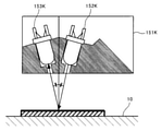
The
図4は、光学センサーユニット150に搭載されたY用の反射型フォトセンサー151Yを示す拡大構成図である。Y用の反射型フォトセンサー151Yは、光源としてのLED152Yと、正反射光を受光する正反射型受光素子153Yと、拡散反射光を受光する拡散反射型受光素子154Yとを具備している。正反射型受光素子153Yは、Yパッチ状トナー像の表面で得られる正反射光の光量に応じた電圧を出力する。また、拡散反射型受光素子154Yは、Yパッチ状トナー像の表面で得られる拡散反射光の光量に応じた電圧を出力する。制御部は、それらの電圧に基づいて、Yパッチ状トナー像のYトナー付着量を算出することができる。Y用の反射型フォトセンサー151Yについて説明したが、C,M用の反射型フォトセンサー151C,151Mも、Y用と同様の構成になっている。
FIG. 4 is an enlarged configuration diagram showing a
図5は、光学センサーユニット150に搭載されたK用の反射型フォトセンサー151Kを示す拡大構成図である。K用の反射型フォトセンサー151Kは、光源たるLED152Kと、正反射光を受光する正反射型受光素子153Kとを具備している。正反射型受光素子153Kは、Kパッチ状トナー像の表面で得られる正反射光の光量に応じた電圧を出力する。制御部は、その電圧に基づいて、Kパッチ状トナー像のKトナー付着量を算出することができる。
FIG. 5 is an enlarged configuration diagram showing a
LED(152Y,C,M,K)としては、発光される光のピーク波長が950nmであるGaAs赤外発光ダイオードを用いている。また、正反射受光素子(153Y,C,M,K)や拡散反射受光素子(154Y,C,M)としては,ピーク受光感度が800nmであるSiフォトトランジスタなどを用いている。但し、ピーク波長やピーク受光感度は前述した値に限られるものではない。 As the LED (152Y, C, M, K), a GaAs infrared light emitting diode having a peak wavelength of emitted light of 950 nm is used. Further, as the specular reflection light receiving element (153Y, C, M, K) and the diffuse reflection light receiving element (154Y, C, M), a Si phototransistor having a peak light receiving sensitivity of 800 nm is used. However, the peak wavelength and the peak light receiving sensitivity are not limited to the above-mentioned values.
四つの反射型フォトセンサーと、中間転写ベルト10のおもて面との間には、5[mm]程度のギャップが設けられている。
A gap of about 5 [mm] is provided between the four reflective photo sensors and the front surface of the
制御部は、主電源の投入時や、所定時間経過した後の待機時、所定枚数以上のプリントを出力したあとの待機時など、所定のタイミングで、プロセスコントロール処理を実施する。そして、プロセスコントロール処理を開始すると、まず、通紙枚数、印字率、温度、湿度などの環境情報を取得した後、作像ユニット18Y,18C,18M,18Kにおけるそれぞれの現像特性を把握する。具体的には、それぞれの色について、現像γと現像開始電圧を算出する。より詳しくは、感光体20Y,20C,20M,20Kを回転させながらそれぞれを一様に帯電せしめる。この帯電については、帯電電源12Y,12C,12M,12Kから出力する帯電バイアスとして、通常のプリント時とは異なるものを出力する。詳しくは、重畳バイアスからなる帯電バイアスの直流電圧及び交流電圧のうち、直流電圧の絶対値を一定の値ではなく、徐々に大きくしていく。
The control unit executes the process control process at a predetermined timing, such as when the main power is turned on, when the standby time is after a predetermined time has elapsed, or when the standby time is after printing a predetermined number of prints or more. Then, when the process control process is started, first, environmental information such as the number of sheets to be printed, the printing rate, the temperature, and the humidity is acquired, and then the development characteristics of the
このような条件で帯電させた感光体20Y,20C,20M,20Kに対し、レーザー書込装置21によるレーザー光の走査を施して、パッチ状Yトナー像,パッチ状Cトナー像、パッチ状Mトナー像、パッチ状Kトナー像用の静電潜像を複数形成する。それらを現像装置80Y,80C,80M,80Kによって現像することで、感光体20Y,20C,20M,20K上にY,C,M,Kパッチパターン像を作像する。このときに、制御部は、各色の第一現像スリーブ及び第二現像スリーブに印加する現像バイアスの絶対値もそれぞれ徐々に大きくしていく。そして、各パッチ状トナー像における静電潜像電位と、現像バイアスとの差分を現像ポテンシャルとしてRAMに記憶する。
The
Y,C,M,Kパッチパターン像は、図6に示されるように、中間転写ベルト10上で重なり合わないように、ベルト幅方向に並んでいる。具体的には、Yパッチパターン像YPPは、中間転写ベルト10の幅方向における一端部に転写される。また、Cパッチパターン像CPPは、ベルト幅方向において、Yパッチパターン像よりも少し中央側にずれた位置に転写される。また、Mパッチパターン像MPPは、中間転写ベルト10の幅方向における他端部に転写される。また、Kパッチパターン像KPPは、ベルト幅方向において、Kパッチパターン像よりも少し中央側にずれた位置に転写される。
As shown in FIG. 6, the Y, C, M, and K patch pattern images are arranged in the belt width direction so as not to overlap on the
光学センサーユニット150は、互いにベルト幅方向の異なる位置でベルトの光反射特性を検知するY用の反射型フォトセンサー151Yを有している。また、C用の反射型フォトセンサー151C、K用の反射型フォトセンサー151K、M用の反射型フォトセンサー151Mも有している。
The
Y用の反射型フォトセンサー151Yは、中間転写ベルト10の幅方向の一端部に形成されたYパッチパターン像YPPのYパッチ状トナー像のYトナー付着量を検知する位置に配設されている。また、第C用の反射型フォトセンサー151Cは、ベルト幅方向において、Yパッチパターン像YPPの近くに位置するCパッチパターン像CPPのCパッチ状トナー像のCトナー付着量を検知する位置に配設されている。また、M用の反射型フォトセンサー151Mは、中間転写ベルト10の幅方向の他端部に形成されたMパッチパターン像MPPのMパッチ状トナー像のMトナー付着量を検知する位置に配設されている。また、K用の反射型フォトセンサー150cは、ベルト幅方向において、Mパッチパターン像MPPの近くに位置するKパッチパターン像KPPのKパッチ状トナー像のKトナー付着量を検知する位置に配設されている。
The
制御部は、光学センサーユニット150の4つの反射型フォトセンサーから順次送られてくる出力信号に基づいて、各色のパッチ状トナー像の光反射率を演算し、演算結果に基づいてトナー付着量を求めてRAMに格納していく。なお、中間転写ベルト10の走行に伴って光学センサーユニット150との対向位置を通過した各色のパッチパターン像は、クリーニング装置によってベルトおもて面からクリーニングされる。
The control unit calculates the light reflectance of the patch-like toner image of each color based on the output signals sequentially sent from the four reflective photosensors of the
制御部は、次に、RAMに格納したトナー付着量と、それとは別にRAMに格納した各パッチトナー像における潜像電位のデータと現像バイアスVbのデータとに基づいて、直線近似式(Y=a×Vp+b)を算出する。具体的には、図7に示されるように、y軸をトナー付着量とし、且つx軸を現像ポテンシャルとする2次元座標における両者の関係を示す近似直線式である。そして、近似直線式に基づいて、目標のトナー付着量を実現する現像ポテンシャルVpを求め、その現像ポテンシャルVpを実現する現像バイアスVbである現像バイアス基準値および帯電バイアス基準値、(およびLDパワー)を求める。 Next, the control unit uses a linear approximation formula (Y =) based on the amount of toner adhered stored in the RAM, the latent image potential data in each patch toner image stored separately in the RAM, and the development bias Vb data. a × Vp + b) is calculated. Specifically, as shown in FIG. 7, it is an approximate linear equation showing the relationship between the two in two-dimensional coordinates where the y-axis is the toner adhesion amount and the x-axis is the development potential. Then, based on the approximate linear equation, the development potential Vp that realizes the target toner adhesion amount is obtained, and the development bias reference value and the charge bias reference value, which are the development bias Vb that realizes the development potential Vp, (and LD power). Ask for.
それらの結果については、不揮発メモリーに記憶する。このような現像バイアス基準値、並びに帯電バイアス基準値(及びLDパワー)の算出及び記憶を、Y,C,M,Kの各色についてそれぞれ行ってプロセスコントロール処理を終了する。その後、プリントジョブにおいては、Y,C,M,Kについてそれぞれ、不揮発性メモリーに記憶している現像バイアス基準値に基づいた値の現像バイアスを、現像電源11Y,11C,11M,11Kから出力させる。また、不揮発性メモリーに記憶している帯電バイアス基準値に基づいた値の帯電バイアスを、帯電電源12Y,12C,12M,12Kから出力させる。
The results are stored in non-volatile memory. Calculation and storage of such a development bias reference value and a charge bias reference value (and LD power) are performed for each of the Y, C, M, and K colors, and the process control process is completed. After that, in the print job, the development bias of the value based on the development bias reference value stored in the non-volatile memory for Y, C, M, and K is output from the
このようなプロセスコントロール処理を実施して目標のトナー付着量を実現する現像バイアス基準値、帯電バイアス基準値を決定することで、Y,C,M,Kの各色についてそれぞれ、画像全体の画像濃度を長期間に渡って安定化させることができる。 By performing such a process control process and determining the development bias reference value and the charge bias reference value that realize the target toner adhesion amount, the image density of the entire image for each of the Y, C, M, and K colors is determined. Can be stabilized over a long period of time.
なお、詳細については後述するが、制御部は、プリントジョブ中において、現像スリーブ回転周期で増減する画像濃度ムラを抑えるために、現像電源11Y,11C,11M,11Kからの現像バイアスの出力値を周期的に変動させる出力変動処理を実施する。しかし、プロセスコントロール処理においては、現像バイアスの出力値を周期変動させずに各色のパッチパターン像の現像を行う。このため、各色のパッチ状トナー像には画像濃度ムラが発生するが、それに起因するトナー付着量の検知精度の低下を抑えるために、それぞれのパッチ状トナー像について、所定の時間間隔で複数回に渡ってトナー付着量を検知し、その平均値を記憶する。
Although the details will be described later, the control unit sets the output value of the development bias from the
次に、本複写機の特徴的な構成について説明する。
図8は、Y用の第一現像スリーブ81Yを示す斜視図である。第一現像スリーブ81Yは、円柱状のローラ部81aY、ローラ部81aYの回転軸線方向の両端面から回転軸線方向に突出する回転軸部材81bYなどを有している。
Next, the characteristic configuration of this copying machine will be described.
FIG. 8 is a perspective view showing the first developing
ローラ部81aYの両端面のそれぞれから突出している回転軸部材81bYの一方は、スリーブ回転センサー76Yを貫いており、スリーブ回転センサー76Yから突出している部分が軸受けによって受けられている。スリーブ回転センサー76Yは、第一現像スリーブ81Yの回転軸部材81bYに固定されて回転軸部材81bYと一体的に回転する遮光部材77Yや、透過型フォトセンサー78Yなどを具備している。遮光部材77Yは、回転軸部材81bYの周面における所定の箇所において法線方向に突出する形状になっている。そして、第一現像スリーブ81Yが所定の回転姿勢になったときに、透過型フォトセンサー78Yの発光素子と受光素子との間に介在する。これにより、受光素子が受光しなくなることで、透過型フォトセンサー78Yからの出力電圧値が大きく低下する。つまり、透過型フォトセンサー78Yは、第一現像スリーブ81Yが所定の回転姿勢になると、そのことを検知して出力電圧値を大きく低下させる。
One of the rotating shaft members 81bY protruding from each of the both end faces of the roller portion 81aY penetrates the
図9は、Y用のスリーブ回転センサー76Yからの出力電圧の経時変化を示すグラフである。なお、スリーブ回転センサー76Yからの出力電圧は、具体的には、透過型フォトセンサー78Yからの出力電圧である。図示のように、第一現像スリーブ81Yが回転しているとき、大半の時間は、スリーブ回転センサー76Yから6[V]の電圧が出力される。但し、第一現像スリーブ81Yが一周する毎に、スリーブ回転センサー76Yからの出力電圧が一瞬だけ0[V]付近まで大きく低下する。これは、第一現像スリーブ81Yが一周する毎に、遮光部材77Yが透過型フォトセンサー78Yの発光素子と受光素子との間に介在して、受光素子が光を受光しなくなるからである。このように出力電圧が大きく低下するタイミングは、第一現像スリーブ81Yが所定の回転姿勢になったタイミングである。以下、このタイミングを基準姿勢タイミングという。
FIG. 9 is a graph showing changes over time in the output voltage from the
Y用のスリーブ回転センサー76Yは、Y用の第一現像スリーブ81Yについて所定の回転姿勢になったことを検知する回転姿勢検知手段として機能している。また、上述したように、第一現像スリーブ81Yと第二現像スリーブ82Yとは同じ回転角速度(=回転周期)で一体的に回転するので、Y用のスリーブ回転センサー76Yは、Y用の第二現像スリーブ82Yについての回転姿勢検知手段としても機能している。
The
図10は、本複写機の電気回路の要部を示すブロック図である。同図において、制御手段としての制御部110は、CPU、RAM、ROM、不揮発性メモリーなどを有している。この制御部110には、Y,C,M,K用の現像装置80Y,80C,80M,80Kのトナー濃度センサー89Y,89C,89M,89Kが電気的に接続されている。これにより、制御部110は、Y,C,M,Kの現像装置80Y,80C,80M,80Kに収容されている現像剤のトナー濃度を把握することができる。
FIG. 10 is a block diagram showing a main part of the electric circuit of this copying machine. In the figure, the control unit 110 as a control means includes a CPU, RAM, ROM, a non-volatile memory, and the like.
制御部110には、Y,C,M,K用のユニット脱着センサー28Y,28C,28M,28Kも電気的に接続されている。脱着検知手段としてのユニット脱着センサー28Y,28C,28M,28Kは、作像ユニット18Y,18C,18M,18Kが画像形成部100から取り外されたことを検知したり、画像形成部100に装着されたことを検知したりすることができる。これにより、制御部110は、画像形成部100に対する作像ユニット18Y,18C,18M,18Kの脱着があったことを把握することができる。
Unit attachment /
また、制御部110には、Y,C,M,K用の現像電源11Y,11C,11M,11Kも電気的に接続されている。制御部110は、現像電源11Y,11C,11M,11Kに制御信号をそれぞれ個別に出力することで、現像電源11Y,11C,11M,11Kから出力される現像バイアスの値を個別に調整することができる。つまり、各色の第一現像スリーブ及び第二現像スリーブの組み合わせ(81Y及び82Y,81C及び82C,81M及び82M,81K及び82K)に印加する現像バイアスの値のそれぞれを個別に調整することができる。
Further, the developing
また、制御部110には、Y,C,M,K用の帯電電源12Y,12C,12M,12Kも電気的に接続されている。制御部110は、帯電電源12Y,12C,12M,12Kに対して制御信号をそれぞれ個別に出力することで、帯電電源12Y,12C,12M,12Kから出力される帯電バイアスにおける直流電圧の値を個別に制御することができる。つまり、Y,C,M,K用の帯電装置19Y,19C,19M,19Kのワイヤーに印加する帯電バイアスの直流電圧の値をそれぞれ個別に調整することができる。
Further, the charging
また、制御部110には、Y,C,M,K用の第一現像スリーブ81Y,81C,81M,81Kについてそれぞれ所定の回転姿勢になったことを個別に検知するためのスリーブ回転センサー76Y,76C,76M,76Kも電気的に接続されている。制御部110は、スリーブ回転センサー76Y,76C,76M,76Kからの出力に基づいて、Y,C,M,K用の第一現像スリーブ81Y,81C,81M,81Kについてそれぞれ所定の回転姿勢になったことを個別に検知することができる。
Further, the control unit 110 has a
制御部110には、書込制御部125、光学センサーユニット150、プロセスモーター120、転写モーター121、レジストモーター122、給紙モーター123なども電気的に接続されている。プロセスモーター120は、作像ユニット18Y,18C,18M,18Kの駆動源になっているモーターである。また、転写モーター121は、中間転写ベルト10の駆動源になっているモーターである。また、レジストモーター122は、レジストローラ対47の駆動源になっているモーターである。また、給紙モーター123は、給紙装置200の給紙カセット201から記録シート5を送り出すためのピックアップローラ202の駆動源になっているモーターである。また、書込制御部125は、画像情報に基づいてレーザー書込装置21の駆動を制御するものである。
The
Y,C,M,Kのトナー像には、現像スリーブ回転周期で増減する画像濃度ムラが発生する。その画像濃度ムラは、現像スリーブの偏心、第一ギャップ変動、第二ギャップ変動、現像スリーブ表面の微妙な歪み、現像スリーブの周方向の電気抵抗ムラなどに起因するものである。第一ギャップ変動は、感光体20Y,20C,20M,20Kと、第一現像スリーブ81Y,81C,81M,81Kとの間の現像ギャップの変動である。また、第二ギャップ変動は、感光体20Y,20C,20M,20Kと、第二現像スリーブ82Y,82C,82M,82Kとの間の現像ギャップの変動である。現像スリーブ回転周期は短時間であることから、画像濃度ムラは副走査方向(感光体表面移動方向)において頁内の短い間隔で出現して目立ってしまう。
In the toner images of Y, C, M, and K, image density unevenness that increases or decreases with the rotation cycle of the developing sleeve occurs. The image density unevenness is caused by the eccentricity of the developing sleeve, the fluctuation of the first gap, the fluctuation of the second gap, the slight distortion of the surface of the developing sleeve, the unevenness of the electrical resistance in the circumferential direction of the developing sleeve, and the like. The first gap variation is a variation in the development gap between the
画像濃度ムラは、具体的には、次のようにして発生する。即ち、第一現像スリーブ81Y,81C,81M,81Kの回転軸が偏心していると、それに起因して、スリーブ一回転あたりでサインカーブ状の変動曲線となるギャップ変動が生ずる。これにより、感光体20Y,20C,20M,20Kと、第一現像スリーブ81Y,81C,81M,81Kとの間に形成される現像電界にも、スリーブ一回転あたりでサインカーブ状の変動曲線となる電界強度変動が生ずる。そして、この電界強度変動により、スリーブ一回転あたりでサインカーブ状の変動曲線となる画像濃度ムラが発生する。また、第一現像スリーブ81Y,81C,81M,81Kの外形には、少なからず歪みがある。この歪みに応じたスリーブ一回転あたりで同じパターンとなる特性の周期的なギャップ変動に起因する画像濃度ムラも発生する。更には、第一現像スリーブ81Y,81C,81M,81Kの周方向の電気抵抗ムラによる周期的な画像濃度ムラも発生する。
Specifically, the image density unevenness occurs as follows. That is, if the rotation axes of the first developing
第一現像スリーブ81Y,81C,81M,81Kの回転に伴って第一現像領域で発生する周期的な画像濃度ムラについて説明したが、第二現像領域でも、同様に、第二現像スリーブ82Y,82C,82M,82Kの回転に伴う周期的な画像濃度ムラが発生する。
Although the periodic image density unevenness that occurs in the first development region due to the rotation of the
そこで、制御部110は、プリントジョブ時において、Y,C,M,Kの各色についてそれぞれ、以下のような出力変動処理を実施する。即ち、制御部110は、Y,C,M,Kの各色についてそれぞれ、スリーブ回転に伴って発生する周期的な画像濃度ムラを相殺することが可能な現像電界強度変動を生じせしめるための現像バイアスの出力パターンデータを不揮発性メモリーに記憶している。以下、この出力パターンデータをバイアス変動データという。 Therefore, the control unit 110 performs the following output fluctuation processing for each of the Y, C, M, and K colors at the time of the print job. That is, the control unit 110 has a development bias for causing fluctuations in the developing electric field strength capable of canceling the periodic image density unevenness generated by the rotation of the sleeve for each of the Y, C, M, and K colors. Output pattern data is stored in the non-volatile memory. Hereinafter, this output pattern data is referred to as bias fluctuation data.
Y,M,C,Kのそれぞれに個別に対応する四つのバイアス変動データは、第一現像スリーブ81Y,81C,81M,81Kの基準姿勢タイミングを基準にしたパターンを表している。それらのバイアス変動データは、プロセスコントロール処理で決定されたY,C,M,K用の現像バイアス基準値を基準にして現像電源(11Y,11C,11M,11K)からの現像バイアスの出力を変化させるためのものである。例えば、データテーブル方式のデータであれば、基準姿勢タイミングからスリーブ回転一周期分の期間内において、所定の時間間隔毎の現像バイアス出力差分を示すデータ群を格納したものになっている。そのデータ群の先頭のデータが基準姿勢タイミングにおける現像バイアス出力差分を示しており、二番目、三番目、四番目・・・のデータが以降における所定の時間間隔毎の現像バイアス出力差分を示している。0、-5、-7、-9・・・というデータ群からなる出力パターンは、基準姿勢タイミングから所定の時間間隔毎の現像バイアス出力差分を0[V]、-5[V]、-7[V]、-9[V]・・・にすることを表している。
The four bias fluctuation data corresponding to each of Y, M, C, and K individually represent a pattern based on the reference posture timing of the first developing
制御部110は、作像処理のときには、Y,C,M,Kのそれぞれに個別に対応するバイアス変動データからのデータの読み込みを所定の時間間隔毎で行う。この読み込みについては、データ群の最後まで読み込んでも基準姿勢タイミングが到来しない場合には、到来するまで読み込み値を最後のデータと同じ値にする。また、データ群の最後まで読み込む前に基準姿勢タイミングが到来した場合には、データの読み込み位置を最初のデータに戻す。 At the time of image drawing processing, the control unit 110 reads data from the bias fluctuation data individually corresponding to each of Y, C, M, and K at predetermined time intervals. Regarding this reading, if the reference posture timing does not arrive even after reading to the end of the data group, the reading value is set to the same value as the last data until it arrives. If the reference posture timing arrives before reading to the end of the data group, the data reading position is returned to the first data.
Y,C,M,Kについてそれぞれ、このようなデータの読み込みを行った結果を、現像バイアス基準値に加算して、加算後の値の現像バイアスが現像電源から出力されるように現像電源を制御する。このような処理を、Y,C,M,Kについてそれぞれ、所定の時間間隔毎に行う。 The results of reading such data for Y, C, M, and K are added to the development bias reference value, and the development power supply is turned on so that the development bias of the added value is output from the development power supply. Control. Such processing is performed for each of Y, C, M, and K at predetermined time intervals.
これにより、感光体20Y,20C,20M,20Kと、第一現像スリーブ81Y,81C,81M,81Kとの間の現像電界に、スリーブ回転に伴って生じる周期的な画像濃度ムラを低減し得る電界強度変動を発生させる。このようにすることで、第一現像スリーブ81Y,81C,81M,81Kの回転姿勢にかかわらず、第一現像スリーブ81Y,81C,81M,81Kの回転に伴ってスリーブ回転周期で発生する画像濃度ムラを抑えることができる。同様にして、第二現像スリーブ82Y,82C,82M,82Kの回転に伴ってスリーブ回転周期で発生する画像濃度ムラを抑えることもできる。
As a result, the electric field that can reduce the periodic image density unevenness caused by the rotation of the sleeve in the developing electric field between the
現像バイアスを出力する現像電源としては、第一現像スリーブ81Yに印加する現像バイアスを出力するための専用のものと、第二現像スリーブ82Yに印加する現像バイアスを出力するための専用のものとを設けるとコストアップを引き起こしてしまう。加えて、スリーブ回転センサーとして、第一現像スリーブ81Yの回転姿勢を検知するものと、第二現像スリーブ82Yの回転姿勢を検知するものとの二つを設けることによるコストアップも引き起こしてしまう。更には、それぞれのスリーブ回転センサーからの出力を個別に監視しながら、監視結果に基づいてそれぞれの現像電源からの出力を制御するための制御部として、高速処理が可能な高価なものを設けることによるコストアップも引き起こしてしまう。
As the development power source for outputting the development bias, a dedicated one for outputting the development bias applied to the
そこで、この複写機では、図10に示されるように、一つの現像電源11Yから出力される周期的に変動する現像バイアスを、第一現像スリーブ81Yと第二現像スリーブ82Yとに印加するようにしている。かかる構成では、現像電源を複数設けることによるコストアップを回避することができる。加えて、スリーブ回転センサーとして、第一現像スリーブ81Yの回転姿勢を検知するスリーブ回転センサー76Yだけを設けているので、スリーブ回転センサーを複数設けることによるコストアップを回避することもできる。更には、複数のスリーブ回転センサーからの出力を個別に監視する必要がないことから、高速処理が可能な高価な制御部を採用することによるコストアップを回避することもできる。C,M,Kについても同様である。
Therefore, in this copying machine, as shown in FIG. 10, a periodically fluctuating development bias output from one developing
周期的な画像濃度ムラは、上述したように、第一現像スリーブ81Yの回転に伴って発生するものと、第二現像スリーブ82Yの回転に伴って発生するものとが存在し、最終的にはそれらの画像濃度ムラが重畳されたムラが画像に現れる。
As described above, there are two types of periodic image density unevenness, one that occurs with the rotation of the first developing
図11は、第一現像スリーブ81Yの偏心に起因して生じるスリーブ回転周期の画像濃度ムラの一例を示すグラフである。同図における縦軸は画像濃度であり、図中の目標値は目標画像濃度を示している。第一現像スリーブ81Yの偏心に起因して、第一現像スリーブ81Yの回転に伴うスリーブ回転周囲の画像濃度ムラは、図示のように、スリーブ一回転あたりで一個分の正弦波を描くパターンで発生するのが一般的である。正弦波における山側のピークでは画像濃度が目標値よりも高くなっているのに対し、谷川のピークでは画像濃度が目標値よりも低くなっている。この正弦波状の画像濃度ムラが第一現像スリーブ81Yの周回毎に発生する。第二現像スリーブ82Yの偏心に起因して第二現像スリーブ82Yの回転に伴って発生するスリーブ回転周期の画像濃度ムラも同様であるが、振幅が第一現像スリーブ81Yのものとは異なっている場合がある。
FIG. 11 is a graph showing an example of image density unevenness in the sleeve rotation cycle caused by the eccentricity of the first developing
図示の例において、画像濃度ムラの波形とは逆位相であって、スリーブ回転周期で増減する変動曲線となるように現像バイアスを変動させたとする。すると、第一現像領域において、第一現像スリーブ81Yの回転姿勢に応じた現像電界の強度変動を、現像バイアスの変動による現像電界の強度変動で相殺して、第一現像スリーブ81Yの回転姿勢にかかわらず、現像電界の強度をほぼ一定にする。これにより、第一現像スリーブ81Yの回転に伴ってスリーブ回転周期で増減する画像濃度ムラをほぼ解消することができる。
In the illustrated example, it is assumed that the development bias is changed so as to have a fluctuation curve that increases or decreases with the sleeve rotation cycle, which is in the opposite phase to the waveform of the image density unevenness. Then, in the first developing region, the fluctuation of the intensity of the developing electric field according to the rotational posture of the first developing
第二現像スリーブ82Yの回転に伴ってスリーブ回転周期で増減する画像濃度ムラについても同様にして抑えることが可能である。但し、この複写機では、第一現像スリーブ81Yと第二現像スリーブ82Yとに対し、共通した現像電源11Yから現像バイアスを出力する。このため、それぞれの現像スリーブに対して画像濃度ムラの波形に対応させた専用の現像バイアスを個別に印加することができない。
It is possible to suppress the image density unevenness that increases or decreases with the rotation cycle of the second developing
以下、便宜上、画像濃度ムラの波形と同じ振幅であって、且つ逆位相の波形の現像バイアスを現像スリーブに印加した場合に、現像スリーブの回転に伴って発生するスリーブ回転周期の画像濃度ムラをゼロできることを前提に説明する。 Hereinafter, for convenience, the image density unevenness of the sleeve rotation cycle that occurs with the rotation of the developing sleeve when a development bias having the same amplitude as the waveform of the image density unevenness and having a waveform of opposite phase is applied to the developing sleeve is shown. The explanation is based on the assumption that it can be zeroed.
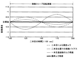
図12は、二つの現像領域のそれぞれで発生する画像濃度ムラの波形と、それらの合成波との第一例を示すグラフである。このグラフは、次のような作像ユニットにおける画像濃度ムラを示している。即ち、第一現像スリーブの回転姿勢をピーク濃度姿勢にするタイミングと、第二現像スリーブの回転姿勢をピーク濃度姿勢にするタイミングとを一致させる条件で、第一現像スリーブ及び第二現像スリーブを現像装置に組み付けた作像ユニットである。ピーク濃度姿勢は、画像濃度ムラの波形の山側ピーク値を出現させる回転姿勢である。以下、前記条件で第一現像スリーブ及び第二現像スリーブを現像装置に組み付けることを、スリーブ回転位相を一致させる、という。また、前者のタイミングと後者のタイミングとをずらす条件で第一現像スリーブ及び第二現像スリーブを現像装置に組み付けることを、スリーブ回転位相をずらす、という。 FIG. 12 is a graph showing a first example of a waveform of image density unevenness generated in each of the two developing regions and a composite wave thereof. This graph shows the image density unevenness in the following image forming unit. That is, the first developing sleeve and the second developing sleeve are developed under the condition that the timing when the rotation posture of the first developing sleeve is changed to the peak density posture and the timing when the rotation posture of the second developing sleeve is changed to the peak density posture are matched. It is an image processing unit assembled to the device. The peak density posture is a rotation posture in which the peak value on the mountain side of the waveform of the image density unevenness appears. Hereinafter, assembling the first developing sleeve and the second developing sleeve to the developing apparatus under the above conditions is referred to as matching the sleeve rotation phases. In addition, assembling the first developing sleeve and the second developing sleeve to the developing device under the condition that the timing of the former and the timing of the latter are shifted is called shifting the sleeve rotation phase.
同図において、一本目による画像濃度ムラは、第一現像スリーブの回転に伴って発生するスリーブ回転周期の画像濃度ムラである。また、二本目による画像濃度ムラは、第二現像スリーブの回転に伴って発生するスリーブ回転周期の画像濃度ムラである。一本目による画像濃度ムラの時間軸は、グラフ枠の下側X軸で示されている。また、二本目による画像濃度ムラの時間軸は、グラフ枠の上側X軸で示されている。 In the figure, the image density unevenness due to the first line is the image density unevenness of the sleeve rotation cycle that occurs with the rotation of the first developing sleeve. Further, the image density unevenness due to the second line is the image density unevenness of the sleeve rotation cycle that occurs with the rotation of the second developing sleeve. The time axis of the image density unevenness due to the first image is shown by the lower X-axis of the graph frame. Further, the time axis of the image density unevenness due to the second line is shown by the upper X-axis of the graph frame.
一本目による画像濃度ムラの時間軸における0[1/100sec]と、二本目による画像濃度ムラの時間軸における100[1/100sec]とが、X軸方向で互いに同じ位置にある。これは、第一現像スリーブ81Yによって0[1/100sec]の時に現像された画像箇所が、第二現像スリーブ82Yによって100[1/100sec]の時に再び現像されることを意味している。二つの現像スリーブの回転周期は互いに100[1/100sec]で同じである。よって、第一現像スリーブと第二現像スリーブとの感光体表面上での配設距離(以下、スリーブ配設距離という)と、感光体の表面がスリーブ回転周期と同じ時間で移動する距離(以下、感光体のスリーブ1周期移動距離という)とが同じになっている。スリーブ配設距離は、図13に示されるように、感光体20Yの表面上における、第一現像スリーブ81Yに最も近づく位置と、第二現像スリーブ82Yに最も近づく位置との距離D1である。
0 [1/100 sec] on the time axis of image density unevenness due to the first image and 100 [1/100 sec] on the time axis of image density unevenness due to the second image are at the same position in the X-axis direction. This means that the image portion developed by the first developing
二つの現像スリーブの回転位相を一致させ、且つスリーブ配設距離を感光体のスリーブ1周期移動距離と同じにした構成では、図示のように、一本目による画像濃度ムラの波形と、二本目による画像濃度ムラの波形とが二本目位置において互いに同位相で重なる。二本目による画像濃度ムラの波形の振幅は、一本目による画像濃度ムラの波形の振幅の半分になっているので、合成波の振幅は一本目による画像濃度ムラの波形の1.5倍になっている。この合成波の位相は、一本目による画像濃度ムラの波形と、二本目による画像濃度ムラの波形とのそれぞれに対して同位相になる。 In the configuration in which the rotation phases of the two developing sleeves are matched and the sleeve arrangement distance is the same as the sleeve one-cycle moving distance of the photoconductor, as shown in the figure, the waveform of the image density unevenness due to the first one and the waveform of the image density unevenness due to the second one are used. The waveforms of image density unevenness overlap each other in the same phase at the second position. Since the amplitude of the waveform of image density unevenness due to the second line is half the amplitude of the waveform of image density unevenness due to the first line, the amplitude of the composite wave is 1.5 times that of the waveform of image density unevenness due to the first line. ing. The phase of this composite wave is in phase with respect to each of the waveform of the image density unevenness due to the first line and the waveform of the image density unevenness due to the second line.
画像濃度の目標値からのずれ量と、補正するための現像バイアスの基準値からのずれ量(正負の極性は前者のずれ量とは逆になる)とを、同一グラフ上で同じ値(絶対値)にする条件でグラフを作成したとする。すると、図12の例では、振幅が合成波の振幅の1/2であって、且つ合成波とは逆位相のパターンで現像バイアスを変動させれば、スリーブ回転周期で増減する画像濃度ムラの発生を回避することができる。この現像バイアスの位相は、感光体表面が第一現像領域に進入するタイミングを基準にした時間軸で示されるものである。現像バイアスを前記パターンで変動させることを前提にして説明する。 The amount of deviation from the target value of image density and the amount of deviation from the reference value of the development bias for correction (positive and negative polarities are opposite to the amount of deviation of the former) are the same value (absolute) on the same graph. It is assumed that the graph is created under the condition of (value). Then, in the example of FIG. 12, if the amplitude is ½ of the amplitude of the composite wave and the development bias is changed in a pattern having a phase opposite to that of the composite wave, the image density unevenness that increases or decreases with the sleeve rotation cycle increases. It can be avoided. The phase of this development bias is shown on the time axis based on the timing at which the surface of the photoconductor enters the first development region. The description will be made on the premise that the development bias is varied by the pattern.
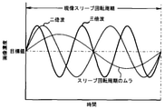
図14は、スリーブ回転位相を一致させ、且つスリーブ配設距離と感光体のスリーブ1周期移動距離とを同じにした場合における第一現像スリーブ関連の各種波形を示すグラフである。第一現像領域では、一本目による画像濃度ムラの波形の山側ピーク値を出現させるタイミングで、現像バイアスの変動波形の谷側ピーク値を出現させる。両ピーク値の絶対値が同じであれば画像濃度を目標値にすることができるが、前記谷側ピーク値の絶対値が前記山側ピーク値の絶対値の0.75倍であることから、0.25の濃度ずれが残る。つまり、一本目通過後のムラ残差の波形は、一本目による画像濃度ムラの波形に対し、同位相で且つ振幅を0.25倍に減少させたものになる。 FIG. 14 is a graph showing various waveforms related to the first developing sleeve when the sleeve rotation phases are matched and the sleeve arrangement distance and the sleeve one-cycle movement distance of the photoconductor are the same. In the first development region, the valley-side peak value of the fluctuation waveform of the development bias appears at the timing when the peak value of the waveform of the image density unevenness due to the first development appears. If the absolute values of both peak values are the same, the image density can be set as the target value, but since the absolute value of the valley side peak value is 0.75 times the absolute value of the mountain side peak value, it is 0. A concentration shift of 0.25 remains. That is, the waveform of the unevenness residual after passing through the first line is in phase with the waveform of the image density unevenness due to the first line, and the amplitude is reduced by 0.25 times.
図15は、スリーブ回転位相を一致させ、且つスリーブ配設距離と感光体のスリーブ1周期移動距離とを同じにした場合における第二現像領域関連の各種波形を示すグラフである。この場合、第二現像領域では、現像バイアスの変動波形(振幅=0.75)に対し、二本目による画像濃度ムラの波形(振幅=0.5)、及び一本目通過後のムラ残差の波形(振幅=0.25)のそれぞれを逆位相で重畳することになる。これにより、現像バイアスの変動波形により、二本目による画像濃度ムラの波形と、一本目通過後のムラ残差の波形とを相殺して、最終ムラ残差を無くすことができる。つまり、第一現像スリーブや第二現像スリーブの回転に伴うスリーブ回転周期の画像濃度ムラの発生を回避することができる。 FIG. 15 is a graph showing various waveforms related to the second developing region when the sleeve rotation phases are matched and the sleeve arrangement distance and the sleeve one-cycle movement distance of the photoconductor are the same. In this case, in the second development region, for the fluctuation waveform of the development bias (amplitude = 0.75), the waveform of the image density unevenness due to the second line (amplitude = 0.5) and the uneven residual after passing the first line. Each of the waveforms (amplitude = 0.25) is superimposed in opposite phase. As a result, the waveform of the image density unevenness due to the second line and the waveform of the unevenness residual after passing through the first line can be offset by the fluctuation waveform of the development bias, and the final uneven residual can be eliminated. That is, it is possible to avoid the occurrence of image density unevenness in the sleeve rotation cycle due to the rotation of the first developing sleeve and the second developing sleeve.
スリーブ回転位相を一致させても、スリーブ配設距離と感光体のスリーブ1周期移動距離とを同じにしなければ、最終ムラ残差の波形は、図15に示される最終ムラ残差の波形とは異なったものになる。本発明者は、スリーブ回転位相を一致させた条件で、スリーブ配設距離の感光体のスリーブ1周期移動距離からのずれ量を様々に変化させて各種の波形の重なり具合を調べるシミュレーションをパーソナルコンピューターで実施した。 Even if the sleeve rotation phases are matched, the waveform of the final unevenness residual is different from the waveform of the final unevenness residual shown in FIG. 15 unless the sleeve arrangement distance and the sleeve 1-cycle movement distance of the photoconductor are the same. It will be different. The present inventor performs a simulation for investigating the overlap of various waveforms by variously changing the amount of deviation of the sleeve arrangement distance from the sleeve one-cycle movement distance of the photoconductor under the condition that the sleeve rotation phases are matched. It was carried out in.
図16は、スリーブ回転位相を一致させ、且つスリーブ配設距離を感光体のスリーブ1/2周期移動距離と同じにした場合における各種の画像濃度ムラ波形を示すグラフである。スリーブ1/2周期移動距離は、感光体の表面がスリーブ回転周期の1/2の時間で移動する距離である。同図では、一本目の時間軸における0[1/100sec]と、二本目の時間軸における50[1/100sec]とが、X軸方向で互いに同じ位置にある。これは、第一現像スリーブ81Yによって0[1/100sec]の時に現像された画像箇所が、第二現像スリーブ82Yによって50[1/100sec]の時に再び現像されることを意味している。第二現像スリーブ82Yによる現像が第一現像スリーブ81Yによる現像から1/2周期だけずれて行われるのである。
FIG. 16 is a graph showing various image density unevenness waveforms when the sleeve rotation phases are matched and the sleeve arrangement distance is the same as the
同図のケースでは、一本目による画像濃度ムラの波形と、二本目による画像濃度ムラの波形とが互いに逆位相で重畳される。それらの合成波は、図示のように、一本目による画像濃度ムラの波形と同位相であって、振幅が同波形の半分になる。半分になる理由は、二本目による画像濃度ムラの波形の振幅が、一本目による画像濃度ムラの波形の振幅の半分だからである。 In the case of the figure, the waveform of the image density unevenness due to the first line and the waveform of the image density unevenness due to the second line are superimposed on each other in opposite phases. As shown in the figure, these combined waves have the same phase as the waveform of the image density unevenness due to the first wave, and the amplitude becomes half of the same waveform. The reason for halving is that the amplitude of the waveform of the image density unevenness due to the second line is half the amplitude of the waveform of the image density unevenness due to the first line.
図17は、スリーブ回転位相を一致させ、且つスリーブ配設距離を感光体のスリーブ1/2周期移動距離と同じにした場合における第二現像領域関連の各種波形を示すグラフである。この場合、図示のように、第二現像領域では、二本目による画像濃度ムラの波形(振幅=0.5)に対し、現像バイアスの変動波形(振幅=0.25)と、一本目通過後のムラ残差の波形(振幅=0.75)とのそれぞれを逆位相で重畳することになる。これにより、最終ムラ残差の波形は、振幅が0.5であって、一本目通過後のムラ残差の波形と同位相になる。図16に示される合成波と、図17に示される最終ムラ残差の波形とを比較すると、両者の振幅は互いに0.5で同じである。これは、現像バイアスを周期変動させたにもかかわらず、最終ムラ残差の濃度最大ずれ量が、現像バイアスを周期変動させない場合に得られる合成波における濃度最大ずれ量と同じであることを意味している。つまり、現像バイアスを周期変動させる場合と、周期変動させない場合とで、画像濃度ムラの度合いが全く変わらないのである。
FIG. 17 is a graph showing various waveforms related to the second developing region when the sleeve rotation phases are matched and the sleeve arrangement distance is the same as the
このような結果になったのは、次に説明する理由による。即ち、第一現像スリーブ81Yの回転に伴う画像濃度ムラと、第二現像スリーブ82Yの回転に伴う画像濃度ムラとが、全く生じない作像ユニットの理想モデルがあると仮定する。この理想モデルでは、現像バイアスを周期変動させると、その周期変動に起因する画像濃度ムラだけが出現する。第一現像領域において、始めの半周期で正弦波の谷側の弧を描き、次の半周期で正弦波の山側の弧を描くパターンで現像バイアスを周期変動させるとする。すると、現像バイアスの挙動は次のようになる。
・現像バイアス
0~半周期目で∪、半周期目~1周期目で∩、1周期目から1.5周期目で∪
The reason for this result is as described below. That is, it is assumed that there is an ideal model of the image forming unit in which the image density unevenness due to the rotation of the first developing
・ Development bias ∪ in the 0th to half cycle, ∩ in the half cycle to the 1st cycle, and ∪ in the 1st to 1.5th cycle
この現像バイアスのパターンでは、第一現像領域において、次のようなパターンの画像濃度ムラ(以下、第一画像濃度ムラ)が生じる。
・第一画像濃度ムラ
0~半周期目で∩、半周期目~1周期目で∪
In this development bias pattern, the following pattern of image density unevenness (hereinafter referred to as first image density unevenness) occurs in the first development region.
・ First image density unevenness ∩ in the 0th to half cycle, ∪ in the half cycle to the 1st cycle
この第一画像濃度ムラは、半周期目~1.5周期目で第二現像領域において生じる画像濃度ムラ(以下、第二画像濃度ムラ)と重畳される。半周期目~1.5周期目では、上に記載したように、∩、∪というパターンで現像バイアスが変動するので、この変動によって生じる第二画像濃度ムラのパターンは次のようになる。
・第二画像濃度ムラ
半周期目~1周期目∪、半周期目~1.5周期目で∩
This first image density unevenness is superimposed on the image density unevenness (hereinafter referred to as the second image density unevenness) that occurs in the second development region in the half cycle to the 1.5th cycle. From the half cycle to the 1.5th cycle, as described above, the development bias fluctuates in the pattern of ∩ and ∪, and the pattern of the second image density unevenness caused by this fluctuation is as follows.
・ Second image density unevenness ∩ in half cycle to first cycle ∪, half cycle to 1.5 cycle ∩
すると、第一現像領域で発生した∩、∪というパターンの第一画像濃度ムラと、第二現像領域で発生する∪、∩というパターンの第二画像濃度ムラとが互いに同じ振幅で重畳されることから、ちょうど相殺されて最終ムラ残差は全くなくなる。つまり、現像バイアスを周期変動させない場合と全く同じ結果になるのである。 Then, the first image density unevenness of the pattern ∩ and ∪ generated in the first development area and the second image density unevenness of the pattern ∪ and ∩ generated in the second development area are superimposed on each other with the same amplitude. Therefore, it is just offset and the final uneven residual is completely eliminated. In other words, the result is exactly the same as when the development bias is not changed periodically.
スリーブ回転位相を一致させ、且つスリーブ配設距離を感光体のスリーブ3/2周期移動距離と同じにした場合についてもシミュレーションを実施した。すると、スリーブ1/2周期移動距離と同じにした場合と同様に、現像バイアスを周期変動させても、最終ムラ残差の波形が現像バイアスを周期変動させない場合の最終ムラ残差の波形と同じになった。よって、スリーブ配設距離を、スリーブ回転周期の1/2に奇数を乗じて得られる解と同じ値の時間で感光体の表面が移動する距離と同じにすると、現像バイアスを周期変動させる効果が表れなくなってしまう。
A simulation was also performed when the sleeve rotation phases were matched and the sleeve arrangement distance was the same as the sleeve 3/2 cycle movement distance of the photoconductor. Then, even if the development bias is periodically changed, the waveform of the final uneven residual is the same as the waveform of the final uneven residual when the development bias is not changed periodically, as in the case where the
なお、一本目による画像濃度ムラの振幅が二本目による画像濃度ムラの振幅よりも大きい場合について説明したが、画像濃度ムラの大小関係を逆にして同様のシミュレーションを行ったところ、逆にしなかった場合と同様の結果が得られた。 The case where the amplitude of the image density unevenness due to the first image is larger than the amplitude of the image density unevenness due to the second image was described, but when the same simulation was performed by reversing the magnitude relationship of the image density unevenness, it was not reversed. Similar results were obtained.
そこで、この複写機においては、スリーブ回転位相を一致させ、且つスリーブ配設距離を、スリーブ回転周期の1/2に奇数を乗じて得られる解とは異なる値の時間で感光体の表面が移動する距離と同じにしている。 Therefore, in this copying machine, the surface of the photoconductor moves in a time different from the solution obtained by matching the sleeve rotation phases and multiplying the sleeve arrangement distance by an odd number by 1/2 of the sleeve rotation cycle. It is the same as the distance to be done.
なお、後述するが、スリーブ回転位相を一致させることは必須ではない。スリーブ回転位相をどのような値にに設定しても一致させた場合と同様の効果を得ることができる。 As will be described later, it is not essential to match the sleeve rotation phases. No matter what value the sleeve rotation phase is set to, the same effect as in the case of matching can be obtained.
また、第一現像スリーブ81Yと第二現像スリーブ82Yとについて、互いに同径のものを用いたが、両者の回転周期(一回転時間)を互いに同じにすれば、両者の径を異ならせてもよい。この場合、両者を互いに異なる角速度で回転させることになるが、一回転に要する時間は互いに同じである。
Further, although the first developing
また、一本目による画像濃度ムラの波形と、二本目による画像濃度ムラの波形とが何れも正弦波である例について説明したが、正弦波でない場合には、同様の結果にはならない場合がある。具体的には、スリーブ配設距離を、スリーブ回転周期の1/2に奇数を乗じて得られる解と同じ値の時間で感光体の表面が移動する距離と同じにしても、現像バイアスを周期変動させることによる最終ムラ残差の抑制効果が得られる場合もある。 Further, the example in which the waveform of the image density unevenness due to the first line and the waveform of the image density unevenness due to the second line are both sine waves has been described, but if the waveform is not a sine wave, the same result may not be obtained. .. Specifically, even if the sleeve arrangement distance is the same as the distance that the surface of the photoconductor moves in the same time as the solution obtained by multiplying 1/2 of the sleeve rotation cycle by an odd number, the development bias is cycled. In some cases, the effect of suppressing the final uneven residual can be obtained by fluctuating.
Y,C,M,Kのそれぞれに個別に対応する四つのバイアス変動データについては、構築処理を所定のタイミングで実施することによって構築する。この所定のタイミングは、工場出荷後の初めのプリントジョブに先立つタイミング(以下、初期起動タイミングという)、作像ユニット18Y,18C,18M,18Kの交換を検知したタイミング(以下、交換検知タイミングという)、及び前回の構築処理を実施したときの環境と現状の環境との差である環境変動量が閾値を超えたタイミングである。初期起動タイミングや、環境変動量が閾値を超えたタイミングでは、Y,C,M,Kの全色についてそれぞれ、バイアス変動データを構築する。これに対し、交換検知タイミングでは、交換が検知された作像ユニットについてだけ、バイアス変動データを構築する。このような構築が可能になるように、作像ユニット18Y,18C,18M,18Kの交換をそれぞれ個別に検知するためのユニット着脱センサー17Y,17C,17M,17K(図10参照)が設けられている。
The four bias fluctuation data corresponding to each of Y, C, M, and K are constructed by executing the construction process at a predetermined timing. This predetermined timing is the timing prior to the first print job after factory shipment (hereinafter referred to as the initial start timing), and the timing when the replacement of the
制御部110は、環境の変動量として、環境たる絶対湿度の変動量を用いる。そして、絶対湿度については、環境センサー124による温度の検知結果と、環境センサー124による相対湿度の検知結果とに基づいて算出する。前回の構築処理の際に、絶対湿度を算出して記憶しておく。そして、以降、環境センサー124による温湿度の検知結果に基づく絶対湿度の算出を定期的に実施し、その値と、絶対湿度の記憶値との差(=環境変動量)が所定の閾値を超えた場合に、新たな構築処理を実施する。 The control unit 110 uses the fluctuation amount of the absolute humidity, which is the environment, as the fluctuation amount of the environment. Then, the absolute humidity is calculated based on the temperature detection result by the environment sensor 124 and the relative humidity detection result by the environment sensor 124. The absolute humidity is calculated and stored at the time of the previous construction process. After that, the absolute humidity is calculated periodically based on the detection result of the temperature and humidity by the environmental sensor 124, and the difference between the value and the stored value of the absolute humidity (= environmental fluctuation amount) exceeds a predetermined threshold value. If so, a new construction process is performed.
初期起動タイミングにおける構築処理では、まず、Yベタトナー像からなるYテストトナー像を感光体20Y上に作像する。また、Cベタトナー像,Mベタトナー像,Kベタトナー像からなるCテストトナー像,Mテストトナー像,Kテストトナー像を、感光体20C,感光体20M,感光体20K上に作像する。そして、それらのテストトナー像を、図18に示されるように、中間転写ベルト10に一次転写する。同図において、Yテストトナー像YITは、感光体20Yの回転周期で発生する画像濃度ムラを検知するためのものであるので、ベルト移動方向において、感光体20Yの周長よりも大きな長さで形成される。同様に、Cテストトナー像CIT,Mテストトナー像MIT,Kテストトナー像KITも、ベルト移動方向の長さが感光体20C,20M,20Kの周長よりも大きくなっている。
In the construction process at the initial start-up timing, first, a Y test toner image composed of a Y solid toner image is formed on the
なお、同図では、便宜上、4つのテストトナー像(YIT,CIT,MIT,KIT)をベルト幅方向に一直線上に並べて形成した例を示している。しかし、実際には、個々のテストトナー像のベルト上における形成位置は、ベルト移動方向において最大で感光体周長と同じ値ほどずれる場合がある。これは、例えば、各色についてそれぞれ、テストトナー像の先端位置と、感光体の周方向における基準位置(基準姿勢タイミングで第一現像領域に進入する感光体表面位置)とを一致させるように、テストトナー像の作像を開始するからである。つまり、各色のテストトナー像は、その先端を感光体の周方向における基準位置に一致させるように作像される。 Note that this figure shows an example in which four test toner images (YIT, CIT, MIT, KIT) are arranged in a straight line in the belt width direction for convenience. However, in reality, the formation position of each test toner image on the belt may deviate by the same value as the peripheral length of the photoconductor at the maximum in the belt moving direction. This is performed, for example, so that the tip position of the test toner image and the reference position in the circumferential direction of the photoconductor (the surface position of the photoconductor that enters the first developing region at the reference posture timing) are matched for each color. This is because the image formation of the toner image is started. That is, the test toner image of each color is imaged so that the tip thereof coincides with the reference position in the circumferential direction of the photoconductor.
テストトナー像として、ベタトナー像に代えて、中間調トナー像を形成していもよい。例えばドット面積率が70[%]である中間調トナー像を形成してもよい。 As the test toner image, a halftone toner image may be formed instead of the solid toner image. For example, a halftone toner image having a dot area ratio of 70 [%] may be formed.
制御部110は、構築処理をプロセスコントロール処理とセットで行うようになっている。具体的には、構築処理を実施する直前でプロセスコントロール処理を実施して各色についてそれぞれ現像バイアス基準値を決定しておく。そして、プロセスコントロール処理の直後に実施する構築処理において、各色についてそれぞれ、プロセスコントロール処理で決定しておいた現像バイアス基準値を一定に出力する条件でテストトナー像を現像する。理論的には、テストトナー像は目標トナー付着量になるように作像されるが、実際には第一現像スリーブ及び第二現像スリーブの回転に伴うスリーブ回転周囲の画像濃度ムラが出現してしまう。 The control unit 110 is configured to perform the construction process as a set with the process control process. Specifically, a process control process is performed immediately before the construction process is performed to determine a development bias reference value for each color. Then, in the construction process performed immediately after the process control process, the test toner image is developed under the condition that the development bias reference value determined in the process control process is output to be constant for each color. Theoretically, the test toner image is imaged so as to reach the target toner adhesion amount, but in reality, uneven image density around the sleeve rotation due to the rotation of the first developing sleeve and the second developing sleeve appears. It ends up.
テストトナー像の作像を開始してから(静電潜像の書き込みを開始してから)、テストトナー像の先端を光学センサーユニット150の反射型フォトセンサーによる検知位置に進入させるまでのタイムラグは、各色毎に異なった値である。但し、同じ色であれば、経時的に一定の値である(以下、この値を書込-検知タイムラグという)。
The time lag from the start of image formation of the test toner image (after the start of writing the electrostatic latent image) to the entry of the tip of the test toner image into the detection position by the reflective photo sensor of the
制御部110は、各色についてそれぞれ書込-検知タイムラグを不揮発性メモリーに予め記憶している。そして、各色についてそれぞれ、テストトナー像の作像を開始した後、書込-検知タイムラグが経過した時点から、反射型フォトセンサーからの出力のサンプリングを開始する。このサンプリングについては、所定の時間間隔毎に繰り返し行う。その時間間隔は、バイアス変動データに基づいて現像バイアスを変動させる出力変動処理において用いる出力パターンデータにおける個々のデータを読み込む時間間隔と同じ値である。制御部110は、各色についてそれぞれ、サンプリングデータに基づいて、トナー付着量(画像濃度)と時間(又は感光体表面位置)との関係を示す画像濃度ムラ波形の式を構築し、その画像濃度ムラ波形から、スリーブ回転周期の画像濃度ムラ波形を抽出する。 The control unit 110 stores the write-detection time lag for each color in the non-volatile memory in advance. Then, after starting the image formation of the test toner image for each color, sampling of the output from the reflective photo sensor is started from the time when the write-detection time lag elapses. This sampling is repeated at predetermined time intervals. The time interval is the same value as the time interval for reading individual data in the output pattern data used in the output fluctuation process for varying the development bias based on the bias variation data. The control unit 110 constructs an image density unevenness waveform formula showing the relationship between the amount of toner adhesion (image density) and time (or the surface position of the photoconductor) based on the sampling data for each color, and the image density unevenness thereof. The image density unevenness waveform of the sleeve rotation cycle is extracted from the waveform.
次に、制御部110は、各色についてそれぞれ、テストトナー像のトナー付着量平均値(画像濃度平均値)を算出する。このトナー付着量平均値は、スリーブ回転周期における画像濃度平均値をほぼ反映した値になる。そこで、制御部110は、そのトナー付着量平均値を基準にして、スリーブ回転周期の画像濃度ムラを相殺するためのバイアス変動データを構築する。具体的には、画像濃度ムラ波形に含まれる複数のトナー付着量データのそれぞれ個別に対応するバイアス出力差分を算出する。そのバイアス出力差分は、トナー付着量平均値を基準にするものである。 Next, the control unit 110 calculates the toner adhesion average value (image density average value) of the test toner image for each color. The average value of the amount of toner adhered is a value that substantially reflects the average value of the image density in the sleeve rotation cycle. Therefore, the control unit 110 constructs bias fluctuation data for canceling the image density unevenness in the sleeve rotation cycle with reference to the average value of the toner adhesion amount. Specifically, the bias output difference corresponding to each of the plurality of toner adhesion amount data included in the image density unevenness waveform is calculated. The bias output difference is based on the average value of the toner adhesion amount.
トナー付着量平均値と同じ値のトナー付着量データに対応するバイアス出力差分については、ゼロとして算出する。また、トナー付着量平均値よりも大きいトナー付着量データに対応するバイアス出力差分については、そのトナー付着量とトナー付着量平均値との差分に応じたプラス極性の値として算出する。プラス極性のバイアス出力差分であるので、マイナス極性の現像バイアスを現像バイアス基準値よりも低い値(絶対値の小さい値)に変化させるデータである。また、トナー付着量平均値よりも小さいトナー付着量データに対応するバイアス出力差分については、そのトナー付着量とトナー付着量平均値との差分に応じたマイナス極性の値として算出する。マイナス極性のバイアス出力差分であるので、マイナス極性の現像バイアスを現像バイアス基準値よりも高い値(絶対値の大きい値)に変化させるデータである。 The bias output difference corresponding to the toner adhesion amount data having the same value as the toner adhesion amount average value is calculated as zero. Further, the bias output difference corresponding to the toner adhesion amount data larger than the toner adhesion amount average value is calculated as a positive polarity value according to the difference between the toner adhesion amount and the toner adhesion amount average value. Since it is a positive polarity bias output difference, it is data that changes the negative polarity development bias to a value lower than the development bias reference value (a value with a small absolute value). Further, the bias output difference corresponding to the toner adhesion amount data smaller than the toner adhesion amount average value is calculated as a negative polarity value according to the difference between the toner adhesion amount and the toner adhesion amount average value. Since it is a negative polarity bias output difference, it is data that changes the negative polarity development bias to a value higher than the development bias reference value (a value having a large absolute value).
このようにして、個々のトナー付着量データに対応するバイアス出力差分を求め、それらを順に並べたデータをバイアス変動データとして構築する。 In this way, the bias output difference corresponding to each toner adhesion amount data is obtained, and the data in which they are arranged in order is constructed as bias fluctuation data.
以上のように、各色についてそれぞれ、構築処理において構築したバイアス変動データを用いて、出力変動処理において現像バイアスVbの現像電源(11Y,11C,11M,11K)からの出力値を変化させる。 As described above, the output value of the development bias Vb from the development power supply (11Y, 11C, 11M, 11K) is changed in the output variation processing by using the bias variation data constructed in the construction process for each color.
なお、感光体のスリーブ1周期移動距離は、感光体の線速に応じて変化する。この複写機では、高速プリントモードと、これよりも遅い線速で感光体を駆動する高画質プリントモードとを切り替え可能であるが、これまで説明してきたスリーブ1周期移動距離は、高画質プリントモードにおける距離である。 The sleeve 1-cycle moving distance of the photoconductor changes according to the linear velocity of the photoconductor. In this copier, it is possible to switch between a high-speed print mode and a high-quality print mode that drives the photoconductor at a slower linear speed, but the sleeve one-cycle movement distance described so far is the high-quality print mode. Is the distance in.
次に、実施形態に係る複写機の構成の一部を他の構成に変形した各変形例について説明する。なお、以下に特筆しない限り、各変形例に係る複写機の構成は実施形態と同様である。
[第一変形例]
上述したように、スリーブ回転位相を一致させ、且つスリーブ配設距離を感光体の1周期移動距離の1/2に奇数を乗じた値とは異ならせる構成を採用すれば、現像バイアスを周期変動させる効果が表れなくなってしまうことを回避することができる。しかしながら、かかる構成であれば、現像バイアスを周期変動させることによる画像濃度ムラの抑制効果を必ず得ることができるか否かについては、検証が必要である。
Next, each modification in which a part of the configuration of the copying machine according to the embodiment is transformed into another configuration will be described. Unless otherwise specified below, the configuration of the copying machine according to each modification is the same as that of the embodiment.
[First modification example]
As described above, if a configuration is adopted in which the sleeve rotation phases are matched and the sleeve arrangement distance is different from the value obtained by multiplying 1/2 of the one-cycle movement distance of the photoconductor by an odd number, the development bias is periodically changed. It is possible to prevent the effect of causing the image from disappearing. However, with such a configuration, it is necessary to verify whether or not the effect of suppressing image density unevenness by changing the development bias periodically can be obtained.
そこで、本発明者は、前述の構成について、感光体のスリーブ1/2周期移動距離に奇数を乗じて得られる解とは異なる値として、様々な値を採用し、それぞれの値にスリーブ配設距離を設定して最終ムラ残差を調べるシミュレーションを行った。具体的には、スリーブ配設距離を前記解と同じ値よりも少しずつずらしていって、一本目による画像濃度ムラと二本目による画像濃度ムラとの合成波や、最終ムラ残差の波形を調べた。すると、スリーブ配設距離を、感光体のスリーブ1周期移動距離に対して0.01~0.49の範囲の値を乗じて得られる解と同じ値にすることで、現像バイアスを周期変動させることによる最終ムラ残差の振幅低減効果が得られた。また、スリーブ配設距離を、感光体のスリーブ1周期移動距離に対して0.51~1.00の範囲の値を乗じて得られる解と同じ値にすることによっても、現像バイアスを周期変動させることによる最終ムラ残差の振幅低減効果が得られた。つまり、スリーブ配設距離を、次のような値に設定することで、現像バイアスを周期変動させることによる最終ムラ残差の振幅低減効果を得ることができる。即ち、感光体のスリーブ1周期移動距離に対して整数(0を含む)と0~0.49との加算値を乗じて得られる解、あるいは、感光体のスリーブ1周期移動距離に対して整数(ゼロを含まない)から0.51~0.99を減じて得られる解、と同じ値である。
Therefore, the present inventor adopts various values for the above-mentioned configuration as different values from the solution obtained by multiplying the
第二現像領域において、一本目通過後のムラ残差の波形と、二本目による画像濃度ムラの波形と、現像バイアスの変動波形との位相の関係は、スリーブ配設距離の他に、スリーブ回転位相にも影響を受ける。これまで、スリーブ回転位相を一致させた例について説明したが、スリーブ回転位相を互いにずらした構成について、画像濃度ムラの合成波の振幅と、最終ムラ残差の振幅との関係をシミュレーションによって調べた。スリーブ回転位相のずれ量については、90°、180°、270°の3通りを採用した。すると、どのずれ量であっても、スリーブ回転位相を一致させた場合と同様の結果になった。つまり、スリーブ回転位相には関係なく、スリーブ配設距離を、感光体のスリーブ1周期移動距離の1/2に奇数を乗じて得られる解とは異なる値、と同じにすることで、現像バイアスを周期変動させることによる最終ムラ残差の抑制効果を得ることができる。 In the second development region, the phase relationship between the waveform of the uneven residual after passing through the first line, the waveform of the image density unevenness due to the second line, and the fluctuation waveform of the development bias is determined by the sleeve rotation as well as the sleeve arrangement distance. It is also affected by the phase. So far, an example in which the sleeve rotation phases are matched has been described, but the relationship between the amplitude of the composite wave of image density unevenness and the amplitude of the final uneven residual is investigated by simulation for the configuration in which the sleeve rotation phases are shifted from each other. .. As for the amount of shift of the sleeve rotation phase, three ways of 90 °, 180 ° and 270 ° were adopted. Then, regardless of the amount of deviation, the same result as in the case where the sleeve rotation phases were matched was obtained. That is, regardless of the sleeve rotation phase, the sleeve arrangement distance is set to the same value as the solution obtained by multiplying 1/2 of the sleeve 1-cycle movement distance of the photoconductor by an odd number, so that the development bias is developed. It is possible to obtain the effect of suppressing the final uneven residual by periodically fluctuating.
そこで、第一変形例に係る複写機では、スリーブ回転位相については制約を設けずに、スリーブ配設距離について、次のような値に設定するという制約を設けている。即ち、感光体のスリーブ1周期移動距離に対して整数(0を含む)と0~0.49との加算値を乗じて得られる解、あるいは、感光体のスリーブ1周期移動距離に対して整数(ゼロを含まない)から0.51~0.99を減じて得られる解、と同じ値である。
Therefore, in the copying machine according to the first modification, the sleeve rotation phase is not restricted, and the sleeve arrangement distance is restricted to the following values. That is, a solution obtained by multiplying the
[第二変形例]
第二変形例に係る複写機では、スリーブ回転位相については制約を設けずに、スリーブ配設距離について、感光体のスリーブ1周期移動距離の整数倍(0を含まない)と同じ値に設定している。かかる構成では、図15を用いて説明したように、現像バイアスを周期変動させることによって、最終ムラ残差をほぼ無くすことができる。
[Second modification]
In the copying machine according to the second modification, the sleeve rotation phase is not restricted, and the sleeve arrangement distance is set to the same value as an integral multiple (not including 0) of the sleeve 1-cycle movement distance of the photoconductor. ing. In such a configuration, as described with reference to FIG. 15, the final uneven residual can be substantially eliminated by periodically varying the development bias.
なお、図15では、スリーブ回転位相を一致させた例について説明しているが、スリーブ回転位相のずれ量をどのような値に設定したとしても、一本目、二本目の画像濃度ムラの合成波は現像スリーブの各周回で互いに同じ形状及び位相になる。このため、感光体表面が第一現像領域に進入するときの時間軸を基準にして、その合成波に比べて振幅が1/スリーブ本数であって且つ逆位相となる現像バイアスを採用することで、最終ムラ残差をほぼ無くすことができる。 Note that FIG. 15 describes an example in which the sleeve rotation phases are matched, but no matter what value the sleeve rotation phase shift amount is set to, the composite wave of the first and second image density unevenness. Have the same shape and phase with each other at each round of the developing sleeve. Therefore, by adopting a development bias in which the amplitude is 1 / sleeve number and the phase is opposite to that of the synthesized wave, with reference to the time axis when the surface of the photoconductor enters the first developing region. , The final uneven residual can be almost eliminated.
[第三変形例]
現像スリーブの電気抵抗ムラや外形歪みによっては、スリーブ回転周期で増減する画像濃度ムラの振幅よりも、スリーブ回転周期の1/整数の周期で増減する画像濃度ムラの振幅が大きくなることも考えられる。以下、スリーブ回転周期の1/2の周期で増減する画像濃度ムラの波形を二倍波という。また、スリーブ回転周期の1/3の周期で増減する画像濃度ムラの波形を三倍波という。
[Third modification example]
Depending on the electrical resistance unevenness and external distortion of the developing sleeve, it is possible that the amplitude of the image density unevenness that increases or decreases in a cycle that is 1 / integer of the sleeve rotation cycle is larger than the amplitude of the image density unevenness that increases or decreases in the sleeve rotation cycle. .. Hereinafter, the waveform of image density unevenness that increases or decreases in a cycle of 1/2 of the sleeve rotation cycle is referred to as a double wave. Further, a waveform of image density unevenness that increases or decreases in a cycle of 1/3 of the sleeve rotation cycle is called a triple wave.
図19は、二倍波、三倍波を説明するためのグラフである。図示のように、二倍波は、スリーブ回転周期で二つ分の正弦波状の波形を発生させる。また、三倍波は、スリーブ回転周期で三つ分の正弦波状の波形を発生させる。 FIG. 19 is a graph for explaining the double wave and the triple wave. As shown, the double wave produces two sinusoidal waveforms in the sleeve rotation period. Further, the triple wave generates a three-fold sinusoidal waveform in the sleeve rotation cycle.
二倍波であれば、スリーブ配設距離を、スリーブ回転周期の1/4に奇数を乗じて得られる解とは異なる値と同じにすることで、現像バイアスを周期変動させる効果が表れなくなってしまうことを回避することができる。 In the case of double wave, by making the sleeve arrangement distance the same as a value different from the solution obtained by multiplying 1/4 of the sleeve rotation period by an odd number, the effect of changing the period of the development bias does not appear. It is possible to avoid it.
また、三倍波であれば、スリーブ配設距離を、スリーブ回転周期の1/4に奇数を乗じて得られる解とは異なる値と同じにすることで、現像バイアスを周期変動させる効果が表れなくなってしまうことを回避することができる。 Further, in the case of a triple wave, the effect of periodically fluctuating the development bias appears by making the sleeve arrangement distance the same as a value different from the solution obtained by multiplying 1/4 of the sleeve rotation cycle by an odd number. It is possible to avoid losing it.
そこで、第三変形例においては、二倍波又は三倍波の画像濃度ムラを抑える狙いで、スリーブ配設距離を、スリーブ回転周期の1/4又は1/6に奇数を乗じて得られる解とは異なる値と同じにしている。現像バイアスについては、一本目による二倍波の画像濃度ムラと、二本目による二倍波の画像濃度ムラとの合成波とは逆位相(振幅は1/2)の変動パターンに従って変動させるようにしている。あるいは、一本目による三倍波の画像濃度ムラと、二本目による三倍波の画像濃度ムラとの合成波とは逆位相(振幅は1/2)の変動パターンに従って変動させるようにしている。 Therefore, in the third modification, the solution obtained by multiplying 1/4 or 1/6 of the sleeve rotation cycle by an odd number for the sleeve arrangement distance with the aim of suppressing the image density unevenness of the double wave or the triple wave. It has the same value as different from. The development bias should be changed according to the fluctuation pattern of the opposite phase (amplitude is 1/2) of the combined wave of the image density unevenness of the double wave due to the first line and the image density unevenness of the double wave due to the second line. ing. Alternatively, the combined wave of the image density unevenness of the triple wave caused by the first line and the image density unevenness of the triple wave caused by the second line is changed according to a fluctuation pattern having an opposite phase (amplitude is 1/2).
スリーブ配設距離の具体例としては、次に掲げる四つの何れかである。
・感光体のスリーブ1/2周期移動距離に対して整数(0を含む)と0~0.49との加算値を乗じて得られる解と同じ値。
・感光体のスリーブ1/2周期移動距離に対して整数(ゼロを含まない)から0.51~0.99を減じて得られる解と同じ値。
・感光体のスリーブ1/3周期移動距離に対して整数(0を含む)と0~0.49との加算値を乗じて得られる解と同じ値。
・感光体のスリーブ1/3周期移動距離に対して整数(ゼロを含まない)から0.51~0.99を減じて得られる解と同じ値。
Specific examples of the sleeve arrangement distance are any of the following four.
-The same value as the solution obtained by multiplying the
-The same value as the solution obtained by subtracting 0.51 to 0.99 from an integer (not including zero) for the
-The same value as the solution obtained by multiplying the
-The same value as the solution obtained by subtracting 0.51 to 0.99 from an integer (not including zero) with respect to the
[第四変形例] [Fourth variant]
第四変形例においては、二倍波又は三倍波を解消する狙いで、スリーブ配設距離を、スリーブ回転周期の1/4又は1/6に偶数を乗じて得られる解と同じ値にしている。かかる構成では、二倍波又は三倍波の画像濃度ムラの発生をほぼ解消することができる。 In the fourth modification, the sleeve arrangement distance is set to the same value as the solution obtained by multiplying 1/4 or 1/6 of the sleeve rotation period by an even number with the aim of eliminating the double wave or the triple wave. There is. With such a configuration, it is possible to substantially eliminate the occurrence of image density unevenness of the double wave or the triple wave.
これまで、Y,C,M,K用の四つの作像ユニット18Y,18C,18M,18Kを設けた複写機について説明したが、作像ユニットを一つしか設けていないモノクロ機にも本発明の適用が可能である。また、各色のトナー像を中間転写ベルトに重ね合わせて一次転写する複写機について説明したが、中間転写ベルトに保持される記録シートに重ね合わせて一次転写する画像形成装置にも、本発明の適用が可能である。また、単色のトナー像を感光体から記録シートに転写する画像形成装置にも、本発明の適用が可能である。
So far, a copying machine provided with four
以上に説明したものは一例であり、次の態様毎に特有の効果を奏する。
[第1態様]
第1態様は、潜像を担持する潜像担持体(例えば感光体20Y)と、前記潜像担持体上の潜像を現像する複数の現像部材(例えば第一現像スリーブ81Y及び第二現像スリーブ82Y)を具備する現像手段(例えば現像装置80Y)とを備え、複数の前記現像部材のそれぞれに印加する現像バイアスを共通の電源(例えば現像電源11Y)から周期的に変動させて出力する画像形成装置であって、複数の前記現像部材の表面のそれぞれを同じ周期で周回移動させ、且つ、複数の前記現像部材のうちの少なくとも一つの表面の無端移動姿勢を検知する姿勢検知手段(例えばスリーブ回転センサー76Y)による検知結果に基づいて前記現像バイアスの出力値を前記周期と同じ周期で変動させることを特徴とするものである。
What has been described above is an example, and has a unique effect in each of the following aspects.
[First aspect]
The first aspect is a latent image carrier (for example, a
第1態様においては、複数の現像部材の表面を互いに同じ周期で周回移動させていることから。複数の現像部材のそれぞれが表面無端移動に伴って発生させる周期的な画像濃度ムラの周期が互いに同じになる。そして、潜像担持体の表面が複数の現像部材による現像位置を順に通過していくと、上流側の現像部材の表面移動に伴って発生した画像濃度ムラと、下流側の現像部材の表面移動に伴って発生する画像濃度ムラとが重畳されていく。互いにどのような位相で重畳されるのかは、上流側の現像部材における表面無端移動の位相と、下流側の現像部材における表面無端移動の位相とのずれ量と、それら現像部材の間の距離とによって決まる。そのずれ量と距離との組み合わせは、互いに同じ周期で表面無端移動する複数の現像部材の各周回で変わらない。このため、最下流側の現像部材による現像位置を通過した後の最終的な画像濃度ムラの波形は、現像部材の各周回で同じものになる。また、互いに同じ周期で表面無端移動する複数の現像部材の少なくとも何れか一つについて姿勢検知手段によって所定の無端移動姿勢を検知したタイミングは、他の現像部材についても所定の無端移動姿勢を検知したタイミングになる。そのタイミングに基づいて、前述した最終的な画像濃度ムラの波形の振幅をより小さくするパターンで現像バイアスを変動させることで、複数の現像部材の表面無端移動に伴って生じる現像部材の表面周回周期の画像濃度ムラを抑えることができる。 In the first aspect, the surfaces of the plurality of developing members are orbiting each other at the same cycle. The periodic image density unevenness generated by each of the plurality of developing members due to the endless movement of the surface becomes the same as each other. Then, when the surface of the latent image carrier passes through the developing positions of the plurality of developing members in order, the image density unevenness generated by the surface movement of the developing member on the upstream side and the surface movement of the developing member on the downstream side occur. The image density unevenness that occurs with this is superimposed. The phase of superimposition on each other depends on the amount of deviation between the phase of surface endless movement in the developing member on the upstream side and the phase of surface endless movement in the developing member on the downstream side, and the distance between the developing members. Depends on. The combination of the amount of deviation and the distance does not change at each round of the plurality of developing members that move endlessly on the surface in the same cycle. Therefore, the waveform of the final image density unevenness after passing through the developing position by the developing member on the most downstream side becomes the same in each round of the developing member. Further, at the timing when a predetermined endless moving posture is detected by the posture detecting means for at least one of a plurality of developing members that move on the same cycle with each other, the predetermined endless moving posture is also detected for the other developing members. It's time. Based on that timing, by varying the development bias in a pattern that reduces the amplitude of the waveform of the final image density unevenness described above, the surface circulation period of the developing member that occurs with the endless movement of the surface of a plurality of developing members. Image density unevenness can be suppressed.
[第2態様]
第2態様は、第1態様であって、複数の前記現像部材のうち、現像工程が最後になる前記現像部材による現像を終えた画像に現れる周期的な画像濃度ムラ波形に対し、複数の前記現像部材のうち、現像工程が最初になる前記現像部材による現像位置に前記潜像担持体の表面が進入するときを基準にした時間軸で逆位相となる波形で、前記現像バイアスを変動させることを特徴とするものである。かかる構成では、最終の現像を終えた画像に現れる周期的な画像濃度ムラ波形とは逆位相の波形で現像バイアスを変動させることで、複数の現像部材の表面無端移動に伴って生じる現像部材の表面周回周期の画像濃度ムラを抑えることができる。
[Second aspect]
The second aspect is the first aspect, wherein among the plurality of the developing members, the plurality of the above-mentioned periodic image density unevenness waveforms appearing in the image developed by the developing member at the end of the developing step. Among the developing members, the development bias is varied with a waveform having an opposite phase on the time axis with respect to the time when the surface of the latent image carrier enters the developing position by the developing member at which the developing process is first. It is characterized by. In such a configuration, the development bias is changed by a waveform having a phase opposite to the periodic image density unevenness waveform appearing in the final developed image, so that the developing member is generated by the endless movement of the surface of the plurality of developing members. It is possible to suppress image density unevenness in the surface circuit cycle.
[第3態様]
第3態様は、第2態様において、前記潜像担持体の表面移動方向に沿って互いに隣り合う上流側の前記現像部材と下流側の前記現像部材とにおける前記潜像担持体の表面上の配設距離を、前記潜像担持体の表面が前記周期の1/2に奇数を乗じて得られる解とは異なる値の時間で移動する距離としたことを特徴とするものである。かかる構成では、既に説明したように、現像部材の回転に伴って正弦波の変動パターンとして出現する画像濃度ムラについて、現像バイアスを周期変動させる効果が表れなくなってしまうことを回避することができる。
[Third aspect]
The third aspect is the arrangement on the surface of the latent image carrier between the developing member on the upstream side and the developing member on the downstream side adjacent to each other along the surface moving direction of the latent image carrier in the second aspect. The setting distance is characterized in that the surface of the latent image carrier moves at a time different from the solution obtained by multiplying 1/2 of the period by an odd number. With such a configuration, as described above, it is possible to avoid the effect of periodically changing the development bias for the image density unevenness that appears as a fluctuation pattern of the sine wave with the rotation of the developing member.
[第4態様]
第4態様は、第3態様において、前記配設距離を、前記周期の1/2に偶数を乗じて得られる解と同じ値の時間で前記潜像担持体の表面が移動する距離としたことを特徴とするものである。かかる構成では、複数の現像部材の表面無端移動に伴って生じる現像部材の表面周回周期の画像濃度ムラをほぼ解消することができる。
[Fourth aspect]
In the fourth aspect, in the third aspect, the arrangement distance is set to the distance at which the surface of the latent image carrier moves in the same time as the solution obtained by multiplying 1/2 of the period by an even number. It is characterized by. With such a configuration, it is possible to substantially eliminate the image density unevenness of the surface circulation cycle of the developing member caused by the endless movement of the surface of the plurality of developing members.
[第5態様]
第5態様は、第2態様において、前記潜像担持体の表面移動方向に沿って互いに隣り合う上流側の前記現像部材と下流側の前記現像部材とにおける前記潜像担持体の表面上の配設距離を、前記周期の1/4に奇数を乗じて得られる解とは異なる値、又は、前記周期の1/6に奇数を乗じて得られる解とは異なる値、の時間で前記潜像担持体の表面が移動する距離としたことを特徴とするものである。かかる構成では、正弦波からなる二倍波又は三倍波として出現する画像濃度ムラについて、現像バイアスを周期変動させる効果が表れなくなってしまうことを回避することができる。
[Fifth aspect]
A fifth aspect is the arrangement on the surface of the latent image carrier between the developing member on the upstream side and the developing member on the downstream side adjacent to each other along the surface moving direction of the latent image carrier in the second aspect. The latent image is set at a value different from the solution obtained by multiplying 1/4 of the period by an odd number, or a value different from the solution obtained by multiplying 1/6 of the period by an odd number. It is characterized in that the distance on which the surface of the carrier moves is set. With such a configuration, it is possible to prevent the effect of periodically changing the development bias from appearing with respect to the image density unevenness appearing as a double wave or a triple wave composed of a sine wave.
[第6態様]
第6態様は、第5態様において、前記配設距離を、前記周期の1/4に偶数を乗じて得られる解と同じ値、又は、前記周期の1/6に偶数を乗じて得られる解と同じ値、の時間で前記潜像担持体の表面が移動する距離としたことを特徴とするものである。かかる構成では、複数の現像部材の表面移動に伴って二倍波又は三倍波として出現する画像濃度ムラをほぼ解消することができる。
[Sixth aspect]
In the sixth aspect, in the fifth aspect, the arrangement distance is the same value as the solution obtained by multiplying 1/4 of the period by an even number, or the solution obtained by multiplying 1/6 of the period by an even number. It is characterized in that the distance is set so that the surface of the latent image carrier moves in the same value and time. With such a configuration, it is possible to substantially eliminate the image density unevenness that appears as a double wave or a triple wave due to the surface movement of the plurality of developing members.
[第7態様]
第7態様は、第2、3、4、5又は6態様であって、前記現像バイアスを一定の値にした条件で前記現像手段によって前記潜像担持体上の潜像を現像して得たテスト画像における、前記周期の毎に同じパターンとなる画像濃度ムラを画像濃度検知手段によって検知した結果に基づいて、前記現像バイアスを周期的に変動させるためのパターンデータを構築する処理を所定のタイミングで実施することを特徴とするものである。かかる構成では、作業者によらずに、複数の現像部材の表面無端移動に伴って発生する画像濃度ムラを抑えることが可能な現像バイアスの変動のパターンデータを自動で構築することができる。
[7th aspect]
The seventh aspect is the second, third, fourth, fifth or sixth aspect, which is obtained by developing a latent image on the latent image carrier by the developing means under the condition that the development bias is set to a constant value. Based on the result of detecting the image density unevenness having the same pattern in each cycle of the test image by the image density detecting means, the process of constructing the pattern data for periodically changing the development bias is performed at a predetermined timing. It is characterized by being carried out in. With such a configuration, it is possible to automatically construct pattern data of fluctuations in development bias that can suppress image density unevenness generated by surfaceless movement of a plurality of developing members regardless of the operator.
[第8態様]
第8態様は、潜像を担持する潜像担持体と、前記潜像担持体上の潜像を現像する複数の現像部材を具備する現像手段とを備え、複数の前記現像バイアスのそれぞれに対して印加するための現像バイアスを共通の電源から周期的に変動させて出力する画像形成装置に搭載される現像手段たる現像装置であって、第1、2、3、4、5、6又は7態様に搭載されることを特徴とするものである。
[8th aspect]
Eighth aspect comprises a latent image carrier carrying a latent image and a developing means including a plurality of developing members for developing the latent image on the latent image carrier, with respect to each of the plurality of development biases. A developing device that is a developing means mounted on an image forming device that periodically changes and outputs a developing bias to be applied from a common power source, and is the first, second, third, fourth, fifth, sixth, or seventh. It is characterized in that it is mounted on an embodiment.
[第9態様]
第9態様は、潜像を担持する潜像担持体と、前記潜像担持体上の潜像を現像する複数の現像部材を具備する現像手段とを備え、複数の前記現像バイアスのそれぞれに対して印加するための現像バイアスを共通の電源から周期的に変動させて出力する画像形成装置に搭載され、少なくとも前記潜像担持体と前記現像手段とが一つのユニットとして構成されて一体的に画像形成装置本体に着脱される作像ユニットであって、第1、2、3、4、5、6又は7態様に搭載されることを特徴とするものである。
[9th aspect]
A ninth aspect comprises a latent image carrier that carries a latent image and a developing means that includes a plurality of developing members that develop a latent image on the latent image carrier, with respect to each of the plurality of development biases. It is mounted on an image forming apparatus that periodically changes and outputs a development bias for applying the image from a common power source, and at least the latent image carrier and the developing means are configured as one unit to integrally image an image. It is an image processing unit that is attached to and detached from the main body of the forming apparatus, and is characterized by being mounted in the first, second, third, fourth, fifth, sixth, or seventh aspects.
11Y,11C,11M,11K:現像電源(電源)
20Y,20C,20M,20K:感光体(潜像担持体)
76Y,76C,76M,76K:スリーブ回転センサー(姿勢検知手段)
80Y,80C,80M,80K:現像装置(現像手段)
81Y,81C,81M,81K:第一現像スリーブ(上流側の現像部材)
82Y,82C,82M,82K:第二現像スリーブ(下流側の現像部材)
110:制御部(制御手段)
11Y, 11C, 11M, 11K: Development power supply (power supply)
20Y, 20C, 20M, 20K: Photoreceptor (latent image carrier)
76Y, 76C, 76M, 76K: Sleeve rotation sensor (posture detection means)
80Y, 80C, 80M, 80K: Developing device (developing means)
81Y, 81C, 81M, 81K: First developing sleeve (upstream developing member)
82Y, 82C, 82M, 82K: Second developing sleeve (developing member on the downstream side)
110: Control unit (control means)
Claims (8)
複数の前記現像部材の表面のそれぞれを同じ周期で周回移動させ、
且つ、複数の前記現像部材のうちの少なくとも一つの表面の無端移動姿勢を検知する姿勢検知手段による検知結果に基づいて前記現像バイアスの出力値を前記周期と同じ周期で変動させるとともに、
複数の前記現像部材のうち、現像工程が最後になる前記現像部材による現像を終えた画像に現れる周期的な画像濃度ムラ波形に対し、複数の前記現像部材のうち、現像工程が最初になる前記現像部材による現像位置に前記潜像担持体の表面が進入するときを基準にした時間軸で逆位相となる波形で、前記現像バイアスを変動させることを特徴とする画像形成装置。 A developing means including a latent image carrier for carrying a latent image and a plurality of developing members for developing a latent image on the latent image carrier is provided, and a development bias applied to each of the plurality of developing members is common. It is an image forming device that periodically fluctuates and outputs from the power supply of
Each of the surfaces of the plurality of developing members is orbited in the same cycle,
Moreover, the output value of the development bias is changed in the same cycle as the cycle based on the detection result by the posture detecting means for detecting the endless movement posture of at least one of the development members .
Of the plurality of developing members, the developing step is the first among the plurality of developing members, with respect to the periodic image density unevenness waveform appearing in the image that has been developed by the developing member. An image forming apparatus characterized in that the development bias is varied with a waveform having an opposite phase on the time axis with respect to the time when the surface of the latent image carrier enters the development position by the developing member .
前記潜像担持体の表面移動方向に沿って互いに隣り合う上流側の前記現像部材と下流側の前記現像部材とにおける前記潜像担持体の表面上の配設距離を、前記潜像担持体の表面が前記周期の1/2に奇数を乗じて得られる解とは異なる値の時間で移動する距離としたことを特徴とする画像形成装置。 In the image forming apparatus of claim 1 ,
The arrangement distance on the surface of the latent image carrier between the developing member on the upstream side and the developing member on the downstream side adjacent to each other along the surface moving direction of the latent image carrier is determined by the latent image carrier. An image forming apparatus characterized in that the surface travels at a distance different from the solution obtained by multiplying 1/2 of the period by an odd number.
前記配設距離を、前記周期の1/2に偶数を乗じて得られる解と同じ値の時間で前記潜像担持体の表面が移動する距離としたことを特徴とする画像形成装置。 In the image forming apparatus of claim 2 ,
An image forming apparatus, characterized in that the arrangement distance is a distance at which the surface of the latent image carrier moves in a time having the same value as the solution obtained by multiplying 1/2 of the period by an even number.
前記潜像担持体の表面移動方向に沿って互いに隣り合う上流側の前記現像部材と下流側の前記現像部材とにおける前記潜像担持体の表面上の配設距離を、前記周期の1/4に奇数を乗じて得られる解とは異なる値、又は、前記周期の1/6に奇数を乗じて得られる解とは異なる値、の時間で前記潜像担持体の表面が移動する距離としたことを特徴とする画像形成装置。 In the image forming apparatus of claim 1 ,
The arrangement distance on the surface of the latent image carrier between the developing member on the upstream side and the developing member on the downstream side adjacent to each other along the surface moving direction of the latent image carrier is 1/4 of the period. The distance at which the surface of the latent image carrier moves in a time different from the solution obtained by multiplying by an odd number or a value different from the solution obtained by multiplying 1/6 of the period by an odd number. An image forming apparatus characterized in that.
前記配設距離を、前記周期の1/4に偶数を乗じて得られる解と同じ値、又は、前記周期の1/6に偶数を乗じて得られる解と同じ値、の時間で前記潜像担持体の表面が移動する距離としたことを特徴とする画像形成装置。 In the image forming apparatus of claim 4 ,
The latent image is the same as the solution obtained by multiplying 1/4 of the period by an even number, or the same value as the solution obtained by multiplying 1/6 of the period by an even number. An image forming apparatus characterized in that the distance on which the surface of the carrier moves is set.
前記現像バイアスを一定の値にした条件で前記現像手段によって前記潜像担持体上の潜像を現像して得たテスト画像における、前記周期の毎に同じパターンとなる画像濃度ムラを画像濃度検知手段によって検知した結果に基づいて、前記現像バイアスを周期的に変動させるためのパターンデータを構築する処理を所定のタイミングで実施することを特徴とする画像形成装置。 The image forming apparatus according to claim 1, 2, 3, 4 or 5 .
Image density detection of image density unevenness that has the same pattern at each cycle in a test image obtained by developing a latent image on the latent image carrier by the developing means under the condition that the development bias is set to a constant value. An image forming apparatus, characterized in that a process of constructing pattern data for periodically changing the development bias is performed at a predetermined timing based on a result detected by the means.
請求項1、2、3、4、5又は6の画像形成装置に搭載されることを特徴とする現像装置。 A developing means including a latent image carrier for carrying a latent image and a plurality of developing members for developing a latent image on the latent image carrier, and for applying to each of the plurality of development biases. It is a developing device that is a developing means mounted on an image forming device that periodically changes and outputs a developing bias from a common power source.
A developing apparatus according to claim 1, 2, 3, 4, 5 or 6 , characterized in that it is mounted on the image forming apparatus.
請求項1、2、3、4、5又は6の画像形成装置に搭載されることを特徴とする作像ユニット。 A developing means including a latent image carrier for carrying a latent image and a plurality of developing members for developing a latent image on the latent image carrier, and for applying to each of the plurality of development biases. It is mounted on an image forming apparatus that periodically changes and outputs a development bias from a common power source, and at least the latent image carrier and the developing means are configured as one unit and integrally attached to and detached from the image forming apparatus main body. It is an image processing unit to be processed
An image forming unit according to claim 1, 2, 3, 4, 5 or 6 , characterized in that it is mounted on the image forming apparatus.
Priority Applications (4)
| Application Number | Priority Date | Filing Date | Title |
|---|---|---|---|
| JP2018028766A JP7015472B2 (en) | 2018-02-21 | 2018-02-21 | Image forming device, developing device and image forming unit |
| US16/273,212 US10503110B2 (en) | 2018-02-21 | 2019-02-12 | Image forming apparatus, developing device, and image forming unit |
| EP19156564.7A EP3531208B1 (en) | 2018-02-21 | 2019-02-12 | Image forming apparatus |
| CN201910125515.7A CN110174829B (en) | 2018-02-21 | 2019-02-20 | Image forming apparatus, developing device and image forming unit |
Applications Claiming Priority (1)
| Application Number | Priority Date | Filing Date | Title |
|---|---|---|---|
| JP2018028766A JP7015472B2 (en) | 2018-02-21 | 2018-02-21 | Image forming device, developing device and image forming unit |
Publications (2)
| Publication Number | Publication Date |
|---|---|
| JP2019144422A JP2019144422A (en) | 2019-08-29 |
| JP7015472B2 true JP7015472B2 (en) | 2022-02-03 |
Family
ID=65411764
Family Applications (1)
| Application Number | Title | Priority Date | Filing Date |
|---|---|---|---|
| JP2018028766A Active JP7015472B2 (en) | 2018-02-21 | 2018-02-21 | Image forming device, developing device and image forming unit |
Country Status (4)
| Country | Link |
|---|---|
| US (1) | US10503110B2 (en) |
| EP (1) | EP3531208B1 (en) |
| JP (1) | JP7015472B2 (en) |
| CN (1) | CN110174829B (en) |
Families Citing this family (3)
| Publication number | Priority date | Publication date | Assignee | Title |
|---|---|---|---|---|
| US10698339B1 (en) * | 2019-05-28 | 2020-06-30 | Lexmark International, Inc. | Color image density calibration in imaging device having common developer voltage |
| US10663891B1 (en) * | 2019-05-28 | 2020-05-26 | Lexmark International, Inc. | Color image density calibration in imaging device having common developer voltage |
| US11307515B2 (en) | 2019-07-31 | 2022-04-19 | Ricoh Company, Ltd. | Developing device with a developer regulator and a stopper |
Citations (3)
| Publication number | Priority date | Publication date | Assignee | Title |
|---|---|---|---|---|
| JP2000098675A (en) | 1998-09-24 | 2000-04-07 | Ricoh Co Ltd | Image forming device |
| JP2002351208A (en) | 2001-05-28 | 2002-12-06 | Canon Inc | Developing device |
| JP2007102126A (en) | 2005-10-07 | 2007-04-19 | Fuji Xerox Co Ltd | Developing device and image forming apparatus |
Family Cites Families (29)
| Publication number | Priority date | Publication date | Assignee | Title |
|---|---|---|---|---|
| US5300987A (en) * | 1992-06-11 | 1994-04-05 | Canon Kabushiki Kaisha | Image forming apparatus which reduces or eliminates density irregularity due to thermal deformation of a developing sleeve |
| JP4000551B2 (en) | 2000-07-07 | 2007-10-31 | リコープリンティングシステムズ株式会社 | Image forming apparatus |
| JP2006091629A (en) | 2004-09-27 | 2006-04-06 | Konica Minolta Business Technologies Inc | Developing device and image forming apparatus |
| JP4617134B2 (en) | 2004-10-20 | 2011-01-19 | キヤノン株式会社 | Image forming apparatus |
| JP2007272193A (en) * | 2006-03-06 | 2007-10-18 | Ricoh Printing Systems Ltd | Image forming device and method |
| JP4986706B2 (en) * | 2007-05-23 | 2012-07-25 | 京セラドキュメントソリューションズ株式会社 | Image density correction method and image forming apparatus using the same |
| US7512366B1 (en) * | 2007-08-03 | 2009-03-31 | Xerox Corporation | Apparatus and methods for loading a donor roll utilizing a slow speed trim roll |
| US7890031B2 (en) | 2007-08-10 | 2011-02-15 | Ricoh Company, Ltd. | Developing device and process cartridge used in image forming apparatus |
| JP5382499B2 (en) | 2008-07-01 | 2014-01-08 | 株式会社リコー | Powder conveying apparatus, image forming apparatus, and process cartridge |
| JP5321159B2 (en) | 2008-07-02 | 2013-10-23 | 株式会社リコー | Developing device, process cartridge, and image forming apparatus |
| JP5299686B2 (en) | 2008-08-08 | 2013-09-25 | 株式会社リコー | Process cartridge and image forming apparatus |
| JP5476871B2 (en) | 2008-11-04 | 2014-04-23 | 株式会社リコー | Developing device, process cartridge, and image forming apparatus |
| JP5531579B2 (en) | 2008-11-27 | 2014-06-25 | 株式会社リコー | Powder supply device, image forming device, and powder container |
| JP5576199B2 (en) | 2010-07-14 | 2014-08-20 | 三井金属鉱業株式会社 | Copper powder for conductive paste and conductive paste |
| JP5790078B2 (en) | 2011-03-30 | 2015-10-07 | 株式会社リコー | Image forming apparatus |
| US9046850B2 (en) | 2011-02-04 | 2015-06-02 | Ricoh Company, Ltd. | Image forming apparatus capable of reducing image density irregularity |
| JP5692642B2 (en) | 2011-02-14 | 2015-04-01 | 株式会社リコー | Developing device, image forming apparatus, and process cartridge |
| JP5765624B2 (en) | 2011-08-19 | 2015-08-19 | 株式会社リコー | Developing device, image forming apparatus, and process cartridge |
| JP5950156B2 (en) | 2011-09-09 | 2016-07-13 | 株式会社リコー | Process cartridge and image forming apparatus |
| JP5888598B2 (en) | 2012-03-13 | 2016-03-22 | 株式会社リコー | Process cartridge and image forming apparatus |
| JP6015252B2 (en) | 2012-08-31 | 2016-10-26 | 株式会社リコー | Developer container, developer supply device, developing device, and image forming apparatus |
| JP6213810B2 (en) * | 2013-03-15 | 2017-10-18 | 株式会社リコー | Image forming apparatus |
| JP6432826B2 (en) | 2014-08-11 | 2018-12-05 | 株式会社リコー | Powder supply device and image forming apparatus |
| JP6440016B2 (en) | 2014-09-04 | 2018-12-19 | 株式会社リコー | Developing device, process cartridge, and image forming apparatus |
| US9658576B2 (en) | 2014-12-11 | 2017-05-23 | Ricoh Company, Ltd. | Developing device, and process cartridge and image forming apparatus incorporating same |
| EP3043212B1 (en) | 2015-01-09 | 2020-07-22 | Ricoh Company, Ltd. | Developing device, process cartridge, and image forming apparatus including same |
| JP6860281B2 (en) | 2015-01-14 | 2021-04-14 | 株式会社リコー | Image forming device |
| JP6195176B2 (en) | 2015-12-22 | 2017-09-13 | 株式会社リコー | Image forming apparatus |
| US10061226B2 (en) | 2016-04-28 | 2018-08-28 | Ricoh Company, Ltd. | Image forming apparatus and image forming method |
-
2018
- 2018-02-21 JP JP2018028766A patent/JP7015472B2/en active Active
-
2019
- 2019-02-12 EP EP19156564.7A patent/EP3531208B1/en active Active
- 2019-02-12 US US16/273,212 patent/US10503110B2/en not_active Expired - Fee Related
- 2019-02-20 CN CN201910125515.7A patent/CN110174829B/en active Active
Patent Citations (3)
| Publication number | Priority date | Publication date | Assignee | Title |
|---|---|---|---|---|
| JP2000098675A (en) | 1998-09-24 | 2000-04-07 | Ricoh Co Ltd | Image forming device |
| JP2002351208A (en) | 2001-05-28 | 2002-12-06 | Canon Inc | Developing device |
| JP2007102126A (en) | 2005-10-07 | 2007-04-19 | Fuji Xerox Co Ltd | Developing device and image forming apparatus |
Also Published As
| Publication number | Publication date |
|---|---|
| US10503110B2 (en) | 2019-12-10 |
| JP2019144422A (en) | 2019-08-29 |
| CN110174829B (en) | 2022-03-29 |
| US20190258199A1 (en) | 2019-08-22 |
| EP3531208B1 (en) | 2023-07-19 |
| EP3531208A1 (en) | 2019-08-28 |
| CN110174829A (en) | 2019-08-27 |
Similar Documents
| Publication | Publication Date | Title |
|---|---|---|
| US10877415B2 (en) | Image forming apparatus | |
| JP6641634B2 (en) | Image forming apparatus and image forming method | |
| JP6566288B2 (en) | Image forming apparatus | |
| JP7015472B2 (en) | Image forming device, developing device and image forming unit | |
| JP2013076983A (en) | Image forming apparatus, and image forming method | |
| JP5081518B2 (en) | Image forming apparatus | |
| JP2016200696A (en) | Image forming apparatus | |
| JP2016051130A (en) | Image forming apparatus | |
| JP6997960B2 (en) | Image forming device | |
| JP7037735B2 (en) | Image forming device | |
| JP6628132B2 (en) | Image forming device | |
| JP4167798B2 (en) | Image forming apparatus | |
| JP2008164656A (en) | Image forming apparatus | |
| JP2018040990A (en) | Image forming apparatus and image forming method | |
| JP6975404B2 (en) | Image forming device | |
| JP6900679B2 (en) | Image forming device and correction method | |
| US9482994B2 (en) | Image forming apparatus | |
| JP6922497B2 (en) | Image forming device and image forming method | |
| JP2016186567A (en) | Image forming apparatus | |
| JP5692643B2 (en) | Image forming apparatus | |
| JP2016200697A (en) | Image forming apparatus | |
| JP2017102166A (en) | Image forming apparatus | |
| JP2004151247A (en) | Image forming apparatus | |
| JP2018101063A (en) | Image forming apparatus | |
| JP2017194647A (en) | Image forming apparatus |
Legal Events
| Date | Code | Title | Description |
|---|---|---|---|
| A621 | Written request for application examination |
Free format text: JAPANESE INTERMEDIATE CODE: A621 Effective date: 20201118 |
|
| A977 | Report on retrieval |
Free format text: JAPANESE INTERMEDIATE CODE: A971007 Effective date: 20210831 |
|
| A131 | Notification of reasons for refusal |
Free format text: JAPANESE INTERMEDIATE CODE: A131 Effective date: 20210903 |
|
| A521 | Request for written amendment filed |
Free format text: JAPANESE INTERMEDIATE CODE: A523 Effective date: 20211019 |
|
| TRDD | Decision of grant or rejection written | ||
| A01 | Written decision to grant a patent or to grant a registration (utility model) |
Free format text: JAPANESE INTERMEDIATE CODE: A01 Effective date: 20211224 |
|
| A61 | First payment of annual fees (during grant procedure) |
Free format text: JAPANESE INTERMEDIATE CODE: A61 Effective date: 20220106 |