JP7011157B2 - Display device manufacturing method and display device - Google Patents
Display device manufacturing method and display device Download PDFInfo
- Publication number
- JP7011157B2 JP7011157B2 JP2017225784A JP2017225784A JP7011157B2 JP 7011157 B2 JP7011157 B2 JP 7011157B2 JP 2017225784 A JP2017225784 A JP 2017225784A JP 2017225784 A JP2017225784 A JP 2017225784A JP 7011157 B2 JP7011157 B2 JP 7011157B2
- Authority
- JP
- Japan
- Prior art keywords
- louver
- substrate
- layer
- electrode
- display device
- Prior art date
- Legal status (The legal status is an assumption and is not a legal conclusion. Google has not performed a legal analysis and makes no representation as to the accuracy of the status listed.)
- Active
Links
Images


Classifications
-
- G—PHYSICS
- G02—OPTICS
- G02F—OPTICAL DEVICES OR ARRANGEMENTS FOR THE CONTROL OF LIGHT BY MODIFICATION OF THE OPTICAL PROPERTIES OF THE MEDIA OF THE ELEMENTS INVOLVED THEREIN; NON-LINEAR OPTICS; FREQUENCY-CHANGING OF LIGHT; OPTICAL LOGIC ELEMENTS; OPTICAL ANALOGUE/DIGITAL CONVERTERS
- G02F1/00—Devices or arrangements for the control of the intensity, colour, phase, polarisation or direction of light arriving from an independent light source, e.g. switching, gating or modulating; Non-linear optics
- G02F1/01—Devices or arrangements for the control of the intensity, colour, phase, polarisation or direction of light arriving from an independent light source, e.g. switching, gating or modulating; Non-linear optics for the control of the intensity, phase, polarisation or colour
- G02F1/13—Devices or arrangements for the control of the intensity, colour, phase, polarisation or direction of light arriving from an independent light source, e.g. switching, gating or modulating; Non-linear optics for the control of the intensity, phase, polarisation or colour based on liquid crystals, e.g. single liquid crystal display cells
- G02F1/133—Constructional arrangements; Operation of liquid crystal cells; Circuit arrangements
- G02F1/1333—Constructional arrangements; Manufacturing methods
- G02F1/1343—Electrodes
-
- G—PHYSICS
- G02—OPTICS
- G02F—OPTICAL DEVICES OR ARRANGEMENTS FOR THE CONTROL OF LIGHT BY MODIFICATION OF THE OPTICAL PROPERTIES OF THE MEDIA OF THE ELEMENTS INVOLVED THEREIN; NON-LINEAR OPTICS; FREQUENCY-CHANGING OF LIGHT; OPTICAL LOGIC ELEMENTS; OPTICAL ANALOGUE/DIGITAL CONVERTERS
- G02F1/00—Devices or arrangements for the control of the intensity, colour, phase, polarisation or direction of light arriving from an independent light source, e.g. switching, gating or modulating; Non-linear optics
- G02F1/01—Devices or arrangements for the control of the intensity, colour, phase, polarisation or direction of light arriving from an independent light source, e.g. switching, gating or modulating; Non-linear optics for the control of the intensity, phase, polarisation or colour
- G02F1/13—Devices or arrangements for the control of the intensity, colour, phase, polarisation or direction of light arriving from an independent light source, e.g. switching, gating or modulating; Non-linear optics for the control of the intensity, phase, polarisation or colour based on liquid crystals, e.g. single liquid crystal display cells
- G02F1/1323—Arrangements for providing a switchable viewing angle
-
- G—PHYSICS
- G02—OPTICS
- G02F—OPTICAL DEVICES OR ARRANGEMENTS FOR THE CONTROL OF LIGHT BY MODIFICATION OF THE OPTICAL PROPERTIES OF THE MEDIA OF THE ELEMENTS INVOLVED THEREIN; NON-LINEAR OPTICS; FREQUENCY-CHANGING OF LIGHT; OPTICAL LOGIC ELEMENTS; OPTICAL ANALOGUE/DIGITAL CONVERTERS
- G02F1/00—Devices or arrangements for the control of the intensity, colour, phase, polarisation or direction of light arriving from an independent light source, e.g. switching, gating or modulating; Non-linear optics
- G02F1/01—Devices or arrangements for the control of the intensity, colour, phase, polarisation or direction of light arriving from an independent light source, e.g. switching, gating or modulating; Non-linear optics for the control of the intensity, phase, polarisation or colour
- G02F1/13—Devices or arrangements for the control of the intensity, colour, phase, polarisation or direction of light arriving from an independent light source, e.g. switching, gating or modulating; Non-linear optics for the control of the intensity, phase, polarisation or colour based on liquid crystals, e.g. single liquid crystal display cells
- G02F1/133—Constructional arrangements; Operation of liquid crystal cells; Circuit arrangements
- G02F1/1333—Constructional arrangements; Manufacturing methods
- G02F1/1335—Structural association of cells with optical devices, e.g. polarisers or reflectors
- G02F1/133509—Filters, e.g. light shielding masks
- G02F1/133514—Colour filters
-
- G—PHYSICS
- G02—OPTICS
- G02F—OPTICAL DEVICES OR ARRANGEMENTS FOR THE CONTROL OF LIGHT BY MODIFICATION OF THE OPTICAL PROPERTIES OF THE MEDIA OF THE ELEMENTS INVOLVED THEREIN; NON-LINEAR OPTICS; FREQUENCY-CHANGING OF LIGHT; OPTICAL LOGIC ELEMENTS; OPTICAL ANALOGUE/DIGITAL CONVERTERS
- G02F1/00—Devices or arrangements for the control of the intensity, colour, phase, polarisation or direction of light arriving from an independent light source, e.g. switching, gating or modulating; Non-linear optics
- G02F1/01—Devices or arrangements for the control of the intensity, colour, phase, polarisation or direction of light arriving from an independent light source, e.g. switching, gating or modulating; Non-linear optics for the control of the intensity, phase, polarisation or colour
- G02F1/13—Devices or arrangements for the control of the intensity, colour, phase, polarisation or direction of light arriving from an independent light source, e.g. switching, gating or modulating; Non-linear optics for the control of the intensity, phase, polarisation or colour based on liquid crystals, e.g. single liquid crystal display cells
- G02F1/133—Constructional arrangements; Operation of liquid crystal cells; Circuit arrangements
- G02F1/1333—Constructional arrangements; Manufacturing methods
- G02F1/1339—Gaskets; Spacers; Sealing of cells
-
- G—PHYSICS
- G02—OPTICS
- G02F—OPTICAL DEVICES OR ARRANGEMENTS FOR THE CONTROL OF LIGHT BY MODIFICATION OF THE OPTICAL PROPERTIES OF THE MEDIA OF THE ELEMENTS INVOLVED THEREIN; NON-LINEAR OPTICS; FREQUENCY-CHANGING OF LIGHT; OPTICAL LOGIC ELEMENTS; OPTICAL ANALOGUE/DIGITAL CONVERTERS
- G02F1/00—Devices or arrangements for the control of the intensity, colour, phase, polarisation or direction of light arriving from an independent light source, e.g. switching, gating or modulating; Non-linear optics
- G02F1/01—Devices or arrangements for the control of the intensity, colour, phase, polarisation or direction of light arriving from an independent light source, e.g. switching, gating or modulating; Non-linear optics for the control of the intensity, phase, polarisation or colour
- G02F1/165—Devices or arrangements for the control of the intensity, colour, phase, polarisation or direction of light arriving from an independent light source, e.g. switching, gating or modulating; Non-linear optics for the control of the intensity, phase, polarisation or colour based on translational movement of particles in a fluid under the influence of an applied field
- G02F1/166—Devices or arrangements for the control of the intensity, colour, phase, polarisation or direction of light arriving from an independent light source, e.g. switching, gating or modulating; Non-linear optics for the control of the intensity, phase, polarisation or colour based on translational movement of particles in a fluid under the influence of an applied field characterised by the electro-optical or magneto-optical effect
- G02F1/167—Devices or arrangements for the control of the intensity, colour, phase, polarisation or direction of light arriving from an independent light source, e.g. switching, gating or modulating; Non-linear optics for the control of the intensity, phase, polarisation or colour based on translational movement of particles in a fluid under the influence of an applied field characterised by the electro-optical or magneto-optical effect by electrophoresis
-
- G—PHYSICS
- G02—OPTICS
- G02F—OPTICAL DEVICES OR ARRANGEMENTS FOR THE CONTROL OF LIGHT BY MODIFICATION OF THE OPTICAL PROPERTIES OF THE MEDIA OF THE ELEMENTS INVOLVED THEREIN; NON-LINEAR OPTICS; FREQUENCY-CHANGING OF LIGHT; OPTICAL LOGIC ELEMENTS; OPTICAL ANALOGUE/DIGITAL CONVERTERS
- G02F1/00—Devices or arrangements for the control of the intensity, colour, phase, polarisation or direction of light arriving from an independent light source, e.g. switching, gating or modulating; Non-linear optics
- G02F1/01—Devices or arrangements for the control of the intensity, colour, phase, polarisation or direction of light arriving from an independent light source, e.g. switching, gating or modulating; Non-linear optics for the control of the intensity, phase, polarisation or colour
- G02F1/165—Devices or arrangements for the control of the intensity, colour, phase, polarisation or direction of light arriving from an independent light source, e.g. switching, gating or modulating; Non-linear optics for the control of the intensity, phase, polarisation or colour based on translational movement of particles in a fluid under the influence of an applied field
- G02F1/1675—Constructional details
- G02F1/1677—Structural association of cells with optical devices, e.g. reflectors or illuminating devices
-
- G—PHYSICS
- G02—OPTICS
- G02F—OPTICAL DEVICES OR ARRANGEMENTS FOR THE CONTROL OF LIGHT BY MODIFICATION OF THE OPTICAL PROPERTIES OF THE MEDIA OF THE ELEMENTS INVOLVED THEREIN; NON-LINEAR OPTICS; FREQUENCY-CHANGING OF LIGHT; OPTICAL LOGIC ELEMENTS; OPTICAL ANALOGUE/DIGITAL CONVERTERS
- G02F1/00—Devices or arrangements for the control of the intensity, colour, phase, polarisation or direction of light arriving from an independent light source, e.g. switching, gating or modulating; Non-linear optics
- G02F1/01—Devices or arrangements for the control of the intensity, colour, phase, polarisation or direction of light arriving from an independent light source, e.g. switching, gating or modulating; Non-linear optics for the control of the intensity, phase, polarisation or colour
- G02F1/165—Devices or arrangements for the control of the intensity, colour, phase, polarisation or direction of light arriving from an independent light source, e.g. switching, gating or modulating; Non-linear optics for the control of the intensity, phase, polarisation or colour based on translational movement of particles in a fluid under the influence of an applied field
- G02F1/1675—Constructional details
- G02F1/1679—Gaskets; Spacers; Sealing of cells; Filling or closing of cells
- G02F1/1681—Gaskets; Spacers; Sealing of cells; Filling or closing of cells having two or more microcells partitioned by walls, e.g. of microcup type
-
- G—PHYSICS
- G02—OPTICS
- G02F—OPTICAL DEVICES OR ARRANGEMENTS FOR THE CONTROL OF LIGHT BY MODIFICATION OF THE OPTICAL PROPERTIES OF THE MEDIA OF THE ELEMENTS INVOLVED THEREIN; NON-LINEAR OPTICS; FREQUENCY-CHANGING OF LIGHT; OPTICAL LOGIC ELEMENTS; OPTICAL ANALOGUE/DIGITAL CONVERTERS
- G02F2201/00—Constructional arrangements not provided for in groups G02F1/00 - G02F7/00
- G02F2201/44—Arrangements combining different electro-active layers, e.g. electrochromic, liquid crystal or electroluminescent layers
Description
本開示は、表示装置の製造方法及び表示装置に関する。 The present disclosure relates to a display device manufacturing method and a display device.
表示装置において周囲からの覗き見を防止してプライバシを保護する要望がある。この要望に応えるデバイスとして、必要な範囲のみ光を透過して、不要な範囲への光を制限する、視野角調整フィルム(ルーバ)が知られている。 There is a demand to protect privacy by preventing peeping from the surroundings in the display device. As a device that meets this demand, a viewing angle adjusting film (louver) that transmits light only in a necessary range and limits light to an unnecessary range is known.
特許文献1(特開2011-141498号公報)は、視野角制限のためのルーバが画素領域の境界に形成されている電気光学装置を開示する。これにより、視野角制限のためのルーバが形成されても、透過率の低下による輝度の低下及び輝度のばらつきを抑制できる。 Patent Document 1 (Japanese Unexamined Patent Publication No. 2011-141498) discloses an electro-optic device in which a louver for limiting the viewing angle is formed at the boundary of a pixel region. As a result, even if a louver for limiting the viewing angle is formed, it is possible to suppress a decrease in brightness and a variation in brightness due to a decrease in transmittance.
しかし、特許文献1のルーバは、スタティックであり、視野角を変化させることができず、広視野角な状態で表示装置を使用することが不可能になる。一方、特許文献2(国際公開2015/122083号)は、電気泳動素子を利用することで、電気的に可視範囲(視野角)を切り替える光学素子を開示する。
However, the louver of
特許文献2に開示されている光学素子により、狭視野角と広視野角との間で切り替えるように、表示装置の視野角を動的に制御することができる。このように電極間の電圧により透過光線方向を変化させる光学素子を、表示装置に一体的に組み込み、視野角を変化させる表示装置の構成要素を削減できる技術が望まれる。 The optical element disclosed in Patent Document 2 can dynamically control the viewing angle of the display device so as to switch between a narrow viewing angle and a wide viewing angle. As described above, a technique is desired in which an optical element that changes the direction of transmitted light rays by a voltage between electrodes is integrally incorporated in a display device, and the number of components of the display device that changes the viewing angle can be reduced.
本開示の一態様は、視野角を変更可能なルーバを含む表示装置の製造方法であって、第1基板の第1主面上に、ルーバを駆動する第1電極層を形成する、第1ステップと、前記第1電極層上に、樹脂層を形成する、第2ステップと、前記樹脂層内に、電気泳動粒子及び分散媒を収容するルーバ溝を形成する、第3ステップと、前記ルーバ溝を有する前記樹脂層上に、前記ルーバ溝を閉じるように、上面が平坦な封止層を形成する、第4ステップと、前記封止層上に、カラーフィルタを形成する、第5ステップと、前記封止層上に、前記ルーバを駆動する第2電極層を形成する、第6ステップと、を含む。 One aspect of the present disclosure is a method of manufacturing a display device including a louver whose viewing angle can be changed, wherein a first electrode layer for driving the louver is formed on a first main surface of a first substrate. A step, a second step of forming a resin layer on the first electrode layer, a third step of forming a louver groove for accommodating electrophoretic particles and a dispersion medium in the resin layer, and the louver. A fourth step of forming a sealing layer having a flat upper surface on the resin layer having a groove so as to close the louver groove, and a fifth step of forming a color filter on the sealing layer. A sixth step of forming a second electrode layer for driving the louver on the sealing layer.
本開示の一態様によれば、電極間の電圧により透過光線方向を変化させる光学素子を、表示装置に一体的に組み込むことができる。 According to one aspect of the present disclosure, an optical element that changes the direction of transmitted light rays by a voltage between electrodes can be integrally incorporated in a display device.
以下、添付図面を参照して実施形態を説明する。実施形態は本発明を実現するための一例に過ぎず、本発明の技術的範囲を限定するものではない。各図において共通の構成については同一の参照符号が付されている。説明をわかりやすくするため、図示した物の寸法、形状については、誇張して記載している場合もある。図において同一種類の要素の内の一部のみが符号で指示されている場合がある。なお、明細書、特許請求の範囲、図面における“第1”、“第2”等の序数は、要素間の関係を明確にするため、及び要素間の混同を防ぐために付している。したがって、これらの序数は、要素を数的に限定しているものではない。 Hereinafter, embodiments will be described with reference to the accompanying drawings. The embodiments are merely examples for realizing the present invention, and do not limit the technical scope of the present invention. The same reference numerals are given to the common configurations in each figure. In order to make the explanation easier to understand, the dimensions and shape of the illustrated object may be exaggerated. In the figure, only a part of the elements of the same type may be indicated by a code. The ordinal numbers such as "first" and "second" in the description, claims, and drawings are attached in order to clarify the relationship between the elements and to prevent confusion between the elements. Therefore, these ordinal numbers do not limit the elements numerically.
<第1実施形態>
[構成]
図1Aは、第1実施形態における、表示装置の構成例の表示領域の画素の一部を示す平面図である。図1Aは、カラーフィルタが形成されているカラーフィルタ基板上の一部構成を示す。表示装置100は、格子状のブラックマトリックス(BM)124に画定された、複数の画素を含む。複数の画素はマトリックス状に配置され、各画素は、赤(R)、緑(G)又は青(B)カラーフィルタ(CF)123を含む。
<First Embodiment>
[Constitution]
FIG. 1A is a plan view showing a part of pixels in a display area of a configuration example of a display device according to the first embodiment. FIG. 1A shows a partial configuration on a color filter substrate on which a color filter is formed. The
本例において、画素(カラーフィルタ)は同一の矩形であるが、異なる形状を有してもよく、その形状は任意である。また、画素配列も任意である。図1Aの例においては、複数の画素のカラーフィルタのうち、一つのカラーフィルタのみが符号123で指示されている。
In this example, the pixels (color filters) are the same rectangle, but may have different shapes, and the shapes are arbitrary. Moreover, the pixel arrangement is also arbitrary. In the example of FIG. 1A, of the color filters of the plurality of pixels, only one color filter is indicated by the
表示装置100は、その視野角(光線方向)を制御するルーバ135を含む。ルーバ135は、格子状である。基板の法線方向(基板における積層方向)において見て(平面視)、ルーバ135の全領域は、ブラックマトリックス124の領域に含まれている。
The
ルーバ135は、図1Aにおいて縦方向(列方向)に延びる複数のルーバ素子133と、左右方向(行方向)の延びる複数のルーバ素子134で構成されている。縦方向と横方向は垂直である。図1Aにおいては、一つの縦方向に延びるルーバ素子及び一つの横方向の延びるルーバ素子のみが、それぞれ、符号133及び134で指示されている。
The
縦方向に延びる複数のルーバ素子133の各ルーバ素子133は、横方向の延びる複数のルーバ素子134それぞれと交差し、交差部それぞれにておいて、複数のルーバ素子134と連続している。同様に、横方向に延びる複数のルーバ素子134の各ルーバ素子134は、縦方向の延びる複数のルーバ素子133それぞれと交差し、交差部それぞれにておいて、複数のルーバ素子133と連続している。ルーバ素子133又は134は、直線状でなくてもよい。例えば、ルーバ素子133又は134は、屈曲を繰り返しながら、縦方向又は横方向に延びていてもよい。
Each
図1Aの例において、格子状のブラックマトリックス124の行数及び列数は、それぞれ、格子状のルーバ135の行数及び列数と一致している。ブラックマトリックス124の行数又は列数は、格子状のルーバ135の行数又は列数よりも多くてもよい。ルーバ135は、ストライプ状であってもよい。例えば、図1Aの例において、ルーバ135は、複数のルーバ素子133が省略され、複数のルーバ素子134のみで構成されていてもよく、複数のルーバ素子134が省略され、複数のルーバ素子133のみで構成されていてもよい。
In the example of FIG. 1A, the number of rows and the number of columns of the grid-like
図1Aの例において、ルーバ135は、画素のカラーフィルタ123の間、つまり、カラーフィルタ123の外側に形成されている。基板の法線方向においてみて、ルーバ135の一部は、カラーフィルタ123と重なってもよい。
In the example of FIG. 1A, the
図1Bは、図1AにおけるBB切断線での表示パネルの断面構造と、表示装置100の制御部に含まれる構成とを、模式的に示す。図1Bは、表示装置100の一部構成を示し、バックライトユニットを含む一部構成は省略されている。
FIG. 1B schematically shows the cross-sectional structure of the display panel at the BB cutting line in FIG. 1A and the configuration included in the control unit of the
表示パネルは、TFT(Thin Film Transistor)基板102と、TFT基板102に対向するカラーフィルタ(CF)基板141とを含む。本例の表示装置100は、液晶表示装置である。TFT基板102とCF基板141との間には、液晶層111が挟まれている。表示装置100はさらに不図示のバックライトユニットを含む。
The display panel includes a TFT (Thin Film Transistor)
なお、TFT基板102及びTFT基板102に積層されている要素からなる構成を、TFTパネルと呼ぶことがある。また、CF基板141及びCF基板141に積層されている要素からなる構成を、CFパネルと呼ぶことがある。
The structure composed of the
TFT基板102は、ガラス又は樹脂からなる絶縁性の透明基板である。典型的には、TFT基板102は、典型的には無色透明である。TFT基板102は、例えば矩形であり、その一つの主面がCF基板141の一つの主面と対向している。TFT基板102は不撓性又は可撓性である。
The
TFT基板102の液晶層111と反対側の主面上に、偏光板101が取り付けられている。TFT基板102の液晶層111に対する主面上には、液晶層111に電界を与えるための液晶駆動電極103と対向電極104とが配列されている。液晶駆動電極103と対向電極104との各ペアが、一つの画素の液晶に電界を与える。与えられえる電界によって、画素の透過光量が変化する。TFT基板102上には、制御する画素を選択するための不図示のTFTアレイが形成されている。TFTは画素の光量を制御するための制御素子である。
A
図1Bに示す構成例は、横電界制御型液晶表示装置である。横電界制御型液晶表示装置は、例えば、IPS(In-Plane Switching)型とFFS(Fringe-Field Switching)型液晶表示装置である。図1Bにおいては、複数の液晶駆動電極のうちの一つのみが符号103で指示されており、複数の対向電極のうちの一つのみが符号で指示104されている。
The configuration example shown in FIG. 1B is a horizontal electric field control type liquid crystal display device. The horizontal electric field control type liquid crystal display device is, for example, an IPS (In-Plane Switching) type liquid crystal display device and an FFS (Fringe-Field Switching) type liquid crystal display device. In FIG. 1B, only one of the plurality of liquid crystal drive electrodes is designated by the
TFT基板102上において、液晶駆動電極103と対向電極104とからなる電極層を覆うように、配向膜105が積層されている。配向膜105は液晶層111と接触して、無電界時の液晶分子の配列状態を規定する。液晶層111の液晶材料は、例えば、ネガ型液晶である。ネガ型の液晶は、表示パネルの主面の法線方向の外部電界による影響を受けにくい。液晶層111はポジ型液晶で構成されていてもよい。
The
CF基板141は、ガラス又は樹脂からなる絶縁層の透明基板である。典型的には、CF基板141は、典型的には無色透明である。CF基板141は、例えば矩形である。CF基板141は不撓性又は可撓性である。CF基板141の液晶層111と反対側の主面上に、偏光板142が取り付けられている。
The
TFT基板102の液晶層111に対する主面上に、ルーバ駆動電極136が形成されている。図1Bの例において、ルーバ駆動電極136は、例えば、連続した1枚の面状の透明金属層である。ルーバ駆動電極136は、例えば、ITO又はIZOで形成され、典型的には無色透明である。
A
ルーバ駆動電極136は、ルーバ135と同様の形状を有していてもよい。例えば、ルーバ駆動電極136は、ルーバ135と同様に、格子状又はストライプ状であってもよい。ルーバ駆動電極136は、CF基板141の法線方向において見て、ルーバ135の全領域を覆うように形成されている。図1Bの例においては、ルーバ135の全領域を覆う面状の透明金属層である。
The
本開示においては、ルーバ素子133に対向し、ルーバ素子133を制御する駆動電極を、ルーバ素子駆動電極と呼ぶ。図1A、1Bの例において、ルーバ素子駆動電極は、連続する一つの金属層であるルーバ駆動電極136の一部であって、ルーバ素子133と完全に重なる部分である。
In the present disclosure, the drive electrode facing the
ルーバ駆動電極136の上に、絶縁性の透明樹脂層132が積層されている。透明樹脂層132内に、ルーバ135が形成されている。透明樹脂層132は、典型的には無色透明である。透明樹脂層132は、例えば光硬化樹脂であって、透明樹脂層132内に、ルーバ135が形成されている。各ルーバ素子133は、透明樹脂層132を、CF基板141の積層方向(図1Bの縦方向)において貫通している。
An insulating
ルーバ素子133の構成の詳細は後述するが、図1Bの例において、ルーバ素子133は、透明樹脂層132に形成されている溝に収容されている、分散媒と有色電気泳動粒子とで構成されている。図1Bの例において、透明樹脂層132はルーバ駆動電極136に接触しているが、透明樹脂層132は、例えば他の絶縁層を介してルーバ駆動電極136上に積層されていてもよい。透明樹脂層132とルーバ駆動電極136との間の絶縁層は、電気泳動粒子とルーバ駆動電極136との接触を防ぐ。
The details of the configuration of the
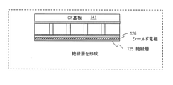
透明樹脂層132の上に、接着層130を介して、絶縁層の封止層131が形成されている。接着層130は、透明樹脂層132及び封止層131に接触しており、透明樹脂層132に対して封止層131を接着する。封止層131は、ルーバ135のために形成されている透明樹脂層132の溝を封止する。封止層131の透明樹脂層132と反対側の面は平坦であり、その上に他の層を適切に積層することができる。
On the
封止層131上に、シールド電極126が積層されている。シールド電極126は接地され(接地電位が与えられ)、ルーバ駆動電極136又は表示装置外部から液晶層111への電界をシールドする。図1Bの例において、シールド電極126は、例えば、連続した1枚の面状の透明金属層である。シールド電極126は、例えば、ITO又はIZOで形成され、典型的には無色透明である。シールド電極126は、ルーバ135の全領域を覆う。シールド電極126は、例えば、全表示領域を覆う。
The
図1Bの構成例において、ルーバ135は、ルーバ駆動電極136とシールド電極126との間に挟まれている。ルーバ135は、ルーバ駆動電極136とシールド電極126との間の電圧に応じて、光の透過量を変化させる。ルーバ駆動電極136及びルーバ駆動電極136と対向するシールド電極126は、それぞれ、ルーバ135を駆動する電極(電極層)である。
In the configuration example of FIG. 1B, the
一つの電極(シールド電極126)が、シールド電極とルーバを駆動する電極として機能することで、表示パネルの要素数を減らすことができ、その結果、表示パネルの厚みを薄くすることができ、さらに、製造効率を高めることができる。なお、シールド電極126は、液晶層111に悪影響を及ぼす電界をシールドすることができれば、どのような形状を有してもよい。
By functioning as one electrode (shield electrode 126) as an electrode for driving the shield electrode and the louver, the number of elements of the display panel can be reduced, and as a result, the thickness of the display panel can be reduced, and further. , Manufacturing efficiency can be improved. The
シールド電極126上に、絶縁層125が積層されている。絶縁層125は、省略されていてもよい。絶縁層125上に、画素を画定する格子状のブラックマトリックス124が積層されている。ブラックマトリックス124は、例えば、黒色樹脂又は、クロム系材料を用いた金属薄膜である。赤、緑、青のいずれかのカラーフィルタ123が、ブラックマトリックス124で囲まれている各画素の領域に形成されている。
An insulating
カラーフィルタ123上に、絶縁性のオーバコート層122が積層されている。オーバコート層122は省略されてもよい。図1Bの例において、カラーフィルタ(CF)層は、上記三色のカラーフィルタ123及びオーバコート層122で構成されている。三色の全てのカラーフィルタ123からなる一つの層を、カラーフィルタ層における色層又はCF色層とも呼ぶ。オーバコート層122上に、配向膜121が積層されている。配向膜121は、液晶層111に接触し、無電界時の液晶分子の配列状態を規定する。
An insulating
不図示のバックライトユニットが、表示パネルの背面(後側)に配置される。TFT基板102又はCF基板141の一方が、画像を視認するユーザが存在する前側であり、他方が後側である。つまり、バックライトユニットは、図1Bが示す表示パネルのTFT基板102側又はCF基板141側に配置される。
A backlight unit (not shown) is arranged on the back (rear side) of the display panel. One of the
バックライトユニットがTFT基板102側に配置されている構成において、ルーバ135は、液晶層111及びカラーフィルタ123を通過した光の出射角度を制御する。バックライトユニットがCF基板141側に配置されている構成において、ルーバ135は、バックライトユニットからカラーフィルタ123に入射する光の角度を制御する。以下においては、バックライトユニットがTFT基板102側に配置されている例を説明する。
In the configuration in which the backlight unit is arranged on the
[動作]
液晶層111は、各画素におけるバックライトユニットからの光の透過量を、液晶駆動電極103と対向電極104との間の電界に応じて制御する。ルーバ135は、通過する光線の方向を制御することで、視野角を制御する機能を有する。表示装置100(ルーバ135)は、広視野角モードと狭視野角モードとを有する。表示装置100からの出射方向の範囲が広いモードを広視野角モードと呼び、出射方向の範囲が狭いモードを狭視野角モードと呼ぶ。
[motion]
The
制御部150は、各画素の液晶駆動電極103と対向電極104それぞれの電位を制御する機能を有する。制御部150は、画像データに応じて、各画素の液晶駆動電極103と対向電極104それぞれの電位を制御して、画素の透過光量を制御する。
The
制御部150は、さらに、シールド電極126とルーバ駆動電極136それぞれの電位を制御する機能を有する。図1Bの例において、制御部150は、シールド電極126を接地電位に維持する。制御部150は、広視野角モード及び狭視野角モードそれぞれにおいて、所定の一定電位をルーバ駆動電極136に与える。制御部150は、例えば、不図示のインタフェースを介したユーザ入力に応じて、広視野角モード及び狭視野角モードを切り替える。
The
図1Bは、狭視野角モードを示す。狭視野角モードにおいて、制御部150は、ルーバ駆動電極136に、接地電位を与える。ルーバ駆動電極136とシールド電極126の電位は同一であり、これらの間の電圧は0Vに維持される。狭視野角モードにおいて、各ルーバ素子133は遮光状態である。
FIG. 1B shows a narrow viewing angle mode. In the narrow viewing angle mode, the
図1Cは、広視野角モードを示す。広視野角モードにおいて、制御部150は、ルーバ駆動電極136に、接地電位より高い所定の電位(正の所定電位)を与える。ルーバ駆動電極136の電位はシールド電極126の電位よりも高く、これらの間の電圧は、ルーバ駆動電極136をプラス電極とする所定電圧に維持される。広視野角モードにおいて、各ルーバ素子133は透過状態である。
FIG. 1C shows a wide viewing angle mode. In the wide viewing angle mode, the
図2Aは、狭視野角モードにおけるルーバ素子133を模式的に示す。図2Bは、広視野角モードにおけるルーバ素子133を模式的に示す。ルーバ素子133は、透明樹脂層132に形成されたルーバ溝137(空間)に収容されている電気泳動粒子139と分散媒138とを含む。電気泳動粒子139は有色であり、例えば、黒色である。分散媒138は例えば無色透明な液体の材料で形成されている。ルーバ135は、分散媒138内の有色電気泳動粒子(有色荷電粒子)139の状態が変化することで、光の透過方向の範囲を変化させる。
FIG. 2A schematically shows the
各ルーバ素子133は、シールド電極126とルーバ駆動電極136とに挟まれている。図2A、2Bの例において、ルーバ駆動電極136は、電気泳動粒子139及び分散媒138からなる電気泳動素子材料に接触している。ルーバ駆動電極136と電気泳動素子材料との間に絶縁層が存在してもよい。絶縁層は、例えば、酸化シリコン又は窒化シリコンである。
Each
図2Aを参照して、狭視野角モードにおいて、ルーバ素子133中の電気泳動粒子139は、分散媒138内に均等に分散している。分散している電気泳動粒子139が光を吸収することで、ルーバ素子133は、カラーフィルタ123からの光を遮蔽する。これにより、狭い出射角度範囲内の光線501のみが、ルーバ135を通過する。
With reference to FIG. 2A, in the narrow viewing angle mode, the
狭視野角モードにおいて、ルーバ素子133を挟むシールド電極126とルーバ駆動電極136とは、同電位(接地電位)に維持される。これにより、電気泳動粒子139は、分散媒138内で拡散し、分散媒138内で均等に分散した状態に維持される。
In the narrow viewing angle mode, the
図2Bを参照して、広視野角モードにおいて、電気泳動粒子139を、ルーバ素子133を挟む電極の一方の近傍に凝集させることにより実現される。図2Bの例においては、電気泳動粒子139は、ルーバ駆動電極136の近傍に凝集している。ルーバ素子133の大部分の領域は透明な分散媒138のみで構成され、ルーバ素子133は透過状態となる。これにより、広い出射角度範囲内の光線501が、ルーバ135を通過する。
It is realized by aggregating the
図2Bの例において、シールド電極126に対するルーバ駆動電極136の相対電位は、電気泳動粒子139の電荷とは逆の極性を有する(電位差V)。これにより、電気泳動粒子139は、ルーバ駆動電極136の近傍に集まる。
In the example of FIG. 2B, the relative potential of the
例えば、電気泳動粒子139の電荷が負(-)であり、ルーバ駆動電極136が正極である場合、電気泳動粒子139は、ルーバ駆動電極136の近傍に集まる。同様に、電気泳動粒子139の電荷が正(+)であり、ルーバ駆動電極136が負極である場合、電気泳動粒子139は、ルーバ駆動電極136の近傍に集まる。電位差Vは、例えば20V~25V程度であればよい。
For example, when the charge of the
反対に、シールド電極126に対するルーバ駆動電極136の相対電位は、電気泳動粒子139の電荷と同一の極性を有してもよい。これにより、電気泳動粒子139は、シールド電極126の近傍に集まる。例えば、電気泳動粒子139の電荷が負(-)であり、ルーバ駆動電極136が負極である場合、電気泳動粒子139は、シールド電極126の近傍に集まる。同様に、電気泳動粒子139の電荷が正(+)であり、ルーバ駆動電極136が正極である場合、電気泳動粒子139は、シールド電極126の近傍に集まる。
Conversely, the relative potential of the
図1Aを参照して説明したように、ルーバ135の全領域は、平面視において、ブラックマトリックス124と重なるように形成されている。電気泳動粒子139は、平面視において、ブラックマトリックス124の領域に含まれるため、広視野角モードにおけるルーバ135での透過率の低下を小さくすることができる。
As described with reference to FIG. 1A, the entire region of the
また、電気泳動粒子139が、ブラックマトリックス124により近い、シールド電極126の近傍に凝集することで、広視野角モードにおける斜め視野において、電気泳動粒子139が表示画素を遮ることが無くなり、視野角特性を向上させることができる。
Further, the
上述のように、ルーバ135をCF基板141上に組み込むことで、アクティブルーバを内包した液晶パネルを薄型化することができる。さらに、ルーバ135の位置をブラックマトリックス124の位置に合わせることで、ルーバ135での透過率低下を小さくすることができる。
As described above, by incorporating the
ルーバ135を駆動する一方の電極は、接地されたシールド電極126である。これにより、ルーバ135の駆動電圧による電界及び装置外部からの電界が液晶層111の駆動に影響を及ぼすことを防ぐことができる。横電界制御型液晶表示装置は、外部からの電界の影響を受けやすいが、ルーバ135の駆動電極の一方がシールド電極として機能することで、専用のシールド電極を省略することができる。
One electrode that drives the
[製造方法]
図1B及び1Cを参照して説明した横電界制御型液晶表示装置100の製造方法の例を、以下に説明する。図3A~図3 は、横電界制御型液晶表示装置100の製造方法の例を示す。
[Production method]
An example of the manufacturing method of the lateral electric field control type liquid
図3Aに示すように、表示装置100の製造は、まず、CF基板141上に、ルーバ駆動電極136を形成する。ルーバ駆動電極136は、例えば、ITO又はIZOからなる、透明導電層である。厚みは、例えば、10~1000nmである。ルーバ駆動電極136の形成は、例えば、スパッタにより透明金属層を付着し、必要であれば、フォトリソグラフィによって所望の形状のルーバ駆動電極136を形成する。
As shown in FIG. 3A, in the manufacture of the
次に、図3Bに示すように、ルーバ駆動電極136の上に、例えば、スピンコーティング又はスリットコーティングにより、透明樹脂301を塗布する。透明樹脂は、例えば、ネガ感光性ポリイミドであり、その粘度は0.1~1Pa・sec、膜厚は30~300μmである。
Next, as shown in FIG. 3B, the
次に、図3Cに示すように、透明樹脂301を、遮光マスク371を介して露光する。遮光マスク371のマスクパターンは、ルーバ溝137の形状に一致する。図3Dに示すように、露光された透明樹脂301を現像して、ルーバ溝137を有する透明樹脂層132を形成する。ルーバ溝137の幅は、例えば、1~40μmであり、ピッチは画素ピッチである。なお、ルーバ溝137と共に外部接続用の開口を透明樹脂層132に形成してもよい。
Next, as shown in FIG. 3C, the
次に、図3Eに示すように、ローラ貼合技術により、透明樹脂層132のルーバ溝137を覆うように、接着層130と封止層131とからなるシートを、透明樹脂層132に付着する。接着層130は、封止層131の透明樹脂層132に対向する面の全面を覆う。硬化前の接着層130が、透明樹脂層132と接触するように、シートは透明樹脂層132上の上に直接に配置される。
Next, as shown in FIG. 3E, a sheet composed of the
接着層130は、例えば、透明熱硬化接着剤で形成されている。接着層130の粘度は例えば、0.1~50Pa・secである。接着層130は、例えば、フレキソ印刷によって、封止層131に予め塗布されている。これにより、効率的にCFパネルを製造することができる。
The
封止層131は、例えば、樹脂又はガラスからなる可撓性の薄いシート(フィルムを含む)である。一例において、封止層131は、5~10μmの厚みを有する透明ポリイミドフィルムである。又は、封止層131は、0.05~0.1mmのフレキシブルガラスである。なお、封止層131は、例えば、外部接続用の孔又は切欠きが形成されていてもよい。
The
次に、図3Fに示すように、接着層130を加熱して、封止層131と透明樹脂層132とをつよく接着する。本例において、接着層130は熱硬化樹脂であり、加熱により接着度が増加する。例えば、接着層130がUV硬化樹脂の場合、UV光が接着層に照射される。接着層130が硬化することで、ルーバ溝137は、封止層131で密閉される。これにより、後工程で使用される薬品や水等のルーバ溝137への侵入を効果的に防ぐことができる。
Next, as shown in FIG. 3F, the
封止層131の表面(露出面)は平坦である。このため、この後の積層工程において、他の層を適切に封止層131上に積層することができる。また、接着層130によって、薄いシートを透明樹脂層132に貼り付けることで、封止層131を形成することができる。このような封止層131により、容易に平坦で封止特性が優れた封止層131を形成することができる。
The surface (exposed surface) of the
次に、図3Gに示すように、封止層131の表面上にシールド電極126を形成する。本例においては、シールド電極126は、封止層131上に直接形成されており、封止層131に接触して界面を形成している。シールド電極126は、封止層131上に、他の中間層を介して形成されていてもよい。
Next, as shown in FIG. 3G, the
シールド電極126は、例えば、ITO又はIZOからなる、透明導電層である。シールド電極126の形成は、例えば、スパッタにより透明金属層を付着し、必要であれば、フォトリソグラフィによって所望の形状のシールド電極126を形成する。本例において、封止層131の全面を覆うようにシールド電極126は形成される。シールド電極126の厚みは、例えば、10~1000nmである。
The
次に、図3Hに示すように、シールド電極126の表面上の全面に、絶縁層125を形成する。絶縁層125は透明有機層であって、例えば、フレキソ印刷によりポリイミド樹脂を塗布することで、形成される。シリコン酸化膜又はシリコン窒化膜をスパッタにより成膜することで、絶縁層125を形成してもよい。絶縁層125は、外部接続用の孔又は凹部を有してもよい。
Next, as shown in FIG. 3H, the insulating
次に、図3Iに示すように、三色のカラーフィルタ123からなるCF色層と、ブラックマトリックス124を、絶縁層125上に形成する。図3Iの例において、カラーフィルタ123及びブラックマトリックス124は、絶縁層125上に直接形成されている。CF色層は、ブラックマトリックス124及び絶縁層125を覆うように形成される。
Next, as shown in FIG. 3I, a CF color layer composed of a three-
本ステップは、まず、ブラックマトリックス124を形成する。例えば、黒色のフォトレジスト(UV硬化樹脂)のパターンをフォトリソグラフィによって形成する。当該パターンが、ブラックマトリックス124である。次に、各色のカラーフィルタ123のパターンを形成する。例えば、各色のカラーフィルタ123のパターンをフォトレジスト(UV硬化樹脂)のフォトリソグラフィによって形成する。CF色層とブラックマトリックス124とは、下層の外部接続用の領域を塞がないように形成される。
This step first forms the
次に、図3Jに示すように、CF色層上に、絶縁性のオーバコート層122を形成する。絶縁性のオーバコート層122は、例えば、エポキシ系又はポリイミド系の熱硬化又はUV硬化樹脂で形成される。樹脂材料を塗布した後、加熱又はUV光を照射することで、オーバコート層122を形成する。オーバコート層122の形成後、オーバコート層122の上に、フォトリソグラフィによって、ポストスペーサを形成してもよい。
Next, as shown in FIG. 3J, an insulating
次に、図3Kに示すように、マザーCF基板351上に形成されている積層体352に切り目を入れる。マザーCF基板351は、複数のCF基板141が切り出される基板である。一つのCF基板141は、複数のCF基板141それぞれに対応する基板部を含む。一つのCF基板141は、マザーCF基板351内又マザーCF基板351から切り出された一つの基板部である。
Next, as shown in FIG. 3K, a cut is made in the
図3A~図3Jを参照して説明した工程は、マザーCF基板351上で、複数のCF基板141に対して同時に行われる。なお、図3A~図3Jを参照して説明した工程は、切り出された一つのCF基板141上で行われてもよい。
The steps described with reference to FIGS. 3A to 3J are simultaneously performed on the
積層体352は、図3A~図3Jを参照して説明した工程で形成された複数層で構成されている。つまり、積層体352は、ルーバ駆動電極136、透明樹脂層132、接着層130、封止層131、ブラックマトリックス124、カラーフィルタ123、オーバコート層122で構成されている。
The
図3Kに示すように、超鋼刃357によって、積層体352に、製品個片354に対応する切り目353を入れる。製品個片354は、一つの表示装置100のCF基板141に対応する。各製品個片354において、表示領域355が定義されている。超鋼刃357に代えて、ダイシングソー、超音波カッタ、又はレーザを使用してもよい。
As shown in FIG. 3K, the
積層体352において、少なくとも透明樹脂層132からオーバコート層122までの層が切断される。以下の説明において、ルーバ駆動電極136も切断されるとするが、ルーバ駆動電極136は切断されなくてもよい。超鋼刃357は、マザーCF基板351にクラックをいれないように、積層体352に切り目353を入れる。
In the
積層体352に切り目が入れられていない場合、マザーCF基板351に対して、積層体352の反対側からスクライビング処理及びブレイキング処理を行うと、積層体352を切断することができない。積層体352の切り目によって、後工程のスクライビング及びブレイキングによって、マザーCF基板351及び積層体352を適切に切断することができる。
When the
次に、CF基板141を含むマザーCF基板351を、組立工程へ投入する。組立工程は、TFTパネル、CFパネル及びそれらの間の液晶層を含む表示パネルを組み立てる。ODF(One Drop Fill)工法又は液晶注入工法のいずれを使用してもよい。
Next, the
ODF工法は、例えば、積層体352が形成されてマザーCF基板351と、TFTアレイを含む基板102上の積層体が形成されているマザーTFT基板(不図示)の一方に液晶を滴下した後に、マザーCF基板351とマザーTFT基板とを貼り合せる。その後、表示パネルを切り出す。
In the ODF method, for example, after the liquid crystal is dropped on one of the
液晶注入工法は、マザーCF基板351とマザーTFT基板とを貼り合せた後、空の表示パネル(セル)又は表示パネル列を切り出し、そこに真空注入により、液晶を注入し、封止する。表示パネル列から、一つのセルが切り出される。
In the liquid crystal injection method, after the
ODF工法又は液晶注入工法における表示パネル(表示セル)の切り出しは、両側の基板に対するスクライビング及びブレイキングを使用する。上述のように、マザーCF基板351(CF基板141)へのスクライビング及びブレイキングの前に、積層体352に切り目が入れられているので、適切に表示パネルを切り出すことができる。 For cutting out the display panel (display cell) in the ODF method or the liquid crystal injection method, scribing and breaking are used for the substrates on both sides. As described above, since the laminate 352 is cut before scribing and breaking to the mother CF substrate 351 (CF substrate 141), the display panel can be appropriately cut out.
組立工程は、CF基板141とTFT基板102との間の接続用導電ペーストの塗布を含む。接続用導電ペーストは、制御部150とCF基板141上の電極、具体的には、ルーバ駆動電極136及びシールド電極126との間の電気的接続に使用される。
The assembly process includes the application of a conductive paste for connection between the
次に、図3Lに示すように、ルーバ溝137に、分散媒138及び電気泳動粒子139を含むルーバ材料を充填し、充填用開口を封止する。さらに、CF基板141及びTFT基板102のそれぞれに、偏光板101及び142を貼り付けた後、液晶駆動用回路部品の接続及びバックライトユニット組み付け等を実施する。
Next, as shown in FIG. 3L, the louver groove 137 is filled with the louver material containing the
図4A~4Eは、ルーバ溝137へのルーバ材料の充填方法を示す。図4Aは、ルーバ材料充填前の表示パネル(個片)を示す。CFパネルの一端413が、TFT基板102より外側に突き出ており、液晶層111の外側で透明樹脂層132及びCF層411を含む積層体が露出している。
4A-4E show a method of filling the louver groove 137 with the louver material. FIG. 4A shows a display panel (individual piece) before filling the louver material. One end 413 of the CF panel protrudes outward from the
CF層411は、カラーフィルタ123及びオーバコート層122からなる層である。CF色層412はカラーフィルタ123からなる層であり、CF層411の一部である。ルーバ溝137は完全に閉じている。
The
図4Bに示すように、CF層411上の露出している積層体の端部に、切り目416を入れる。少なくとも、透明樹脂層132、封止層131、CF層411が、積層方向において切断される。切り目位置は、ルーバ溝137と重なっている。切り目は、例えば、超硬刃、ダイシングソー、超音波カッタ、レーザ等で形成することができる。
As shown in FIG. 4B, a
次に、図4Cに示すように、透明樹脂層132とCF層411が積層されているCF基板141の主面の反対面において、積層体の切り目位置と対向する位置に、スクライブによりクラックを入れる。その後、ブレイキングによって、CF基板141の端部、及び、透明樹脂層132とCF層411とを含む積層体の端部を、切り取る。
Next, as shown in FIG. 4C, a crack is formed by scribe at a position facing the cut position of the laminated body on the opposite surface of the main surface of the
これにより、ルーバ溝137の端部に、開口(ルーバ開口)145が形成される。CF基板141のブレイキングの前に、透明樹脂層132、封止層131、CF層411を含む積層体を積層方向において切断するので、ブレイキングによって、CF基板141及びその上の積層体の端部(CFパネルの端部)を、適切に切り取ることができる。
As a result, an opening (louver opening) 145 is formed at the end of the louver groove 137. Before breaking the
次に、図4Dに示すように、真空注入によって、ルーバ溝137にルーバ材料417を注入する。具体的には、まず、真空槽418内にルーバ溝137を配置し、真空槽418内を真空にする(減圧する)。ルーバ材料417は真空槽418内に設置された容器に収容されている。次に、表示パネルのルーバ溝137のルーバ開口145を含む部分を、ルーバ材料417に浸漬する。その後、真空槽418の真空を解除する。これにより、ルーバ開口145からルーバ材料417が、ルーバ溝137内に侵入する。
Next, as shown in FIG. 4D, the louver material 417 is injected into the louver groove 137 by vacuum injection. Specifically, first, the louver groove 137 is arranged in the vacuum chamber 418, and the inside of the vacuum chamber 418 is evacuated (reduced). The louver material 417 is housed in a container installed in the vacuum chamber 418. Next, the portion of the display panel including the
次に、図4Eに示すように、ルーバ溝137のルーバ開口145を封止材419で閉じする。これにより、ルーバ材料417を収容しているルーバ溝137が再密閉される。なお、他の方法によって、ルーバ材料417をルーバ溝137に充填してもよい。
Next, as shown in FIG. 4E, the
上記製造方法は、図3Eを参照して説明したように、接着層130となる接着剤が付着している封止層131を、透明樹脂層132に貼り付ける。図5A~図5Cは、接着層130及び封止層131を形成する他の方法を示す。
In the above manufacturing method, as described with reference to FIG. 3E, the
図5Aに示すように、フレキソ印刷によって、接着層310を透明樹脂層132の表面(頂面)に形成する。接着層310は、透明樹脂層132のルーバ溝137の外側表面にのみ形成される。次に、ローラを使用して、封止層131となるシートを、接着層310に貼り付ける。封止層131の一部が、ルーバ溝137に露出している。次に、接着層130を加熱して、封止層131と透明樹脂層132とを強く接着する。
As shown in FIG. 5A, the adhesive layer 310 is formed on the surface (top surface) of the
次に、図5Cに示すように、シールド電極126及びシールド電極と外部接続用配線とを接続する端子部を含む導電パターンを形成する。導電パターンの形成は、例えば、ITOやIZO等の透明導体膜を付着し、フォトリソグラフィにより所望のパターンを形成する。図5Cの例において、シールド電極126はルーバ溝137が積層方向において重なるように形成された網目状を有する。これにより、CFパネルの光の透過率を上げることができる。
Next, as shown in FIG. 5C, a conductive pattern including the
<第2実施形態>
図6Aは、第2実施形態に係る表示装置100の構成を模式的に示す。図6Aは、表示パネルの断面構造と、表示装置100の制御部に含まれる構成とを、模式的に示す。図6Aは、表示装置100の一部構成を示し、バックライトユニットを含む一部構成は省略されている。以下において、第1実施形態との相違点を主に説明する。
<Second Embodiment>
FIG. 6A schematically shows the configuration of the
TFT基板102上に、液晶駆動電極103及び対向電極104に代わり、画素電極107が形成されている。画素電極107は、対応する画素の液晶に電界を印加する液晶駆動電極である。画素電極107は、透明電極であり、例えば、ITO又はIZOで形成されている。
A
CF基板141上に、シールド電極126に代えて、対向電極127が積層されている。対向電極127は、配向膜121とオーバコート層122の間に形成されている。対向電極127は、連続する面状の透明電極であり、例えば、ITO又はIZOで形成されている。対向電極127は、画素に共通である。
A
図6Aに示す構成例は、縦電界制御型液晶表示装置である。縦電界制御型液晶表示装置は、例えば、TN(Twisted Nematic)型とVA(Vertical Alignment)型液晶表示装置である。図6Aにおいては、複数の画素電極のうちの一つのみが符号107で指示されている。液晶層111における各画素の液晶は、対向電極127と画素電極107とに挟まれており、これらの間の電圧によって、画素における液晶の向き及び透過光量が変化する。
The configuration example shown in FIG. 6A is a vertical electric field control type liquid crystal display device. The vertical electric field control type liquid crystal display device is, for example, a TN (Twisted Nematic) type liquid crystal display device and a VA (Vertical Element) type liquid crystal display device. In FIG. 6A, only one of the plurality of pixel electrodes is designated by
制御部150は、対向電極127に所定の電位(COM電位)を与えるVCOM回路151を含む。VCOM回路151は、一定又は特定のタイミングで変化する電位信号を対向電極127に与える。
The
ルーバ135は、ルーバ駆動電極136と対向電極127との間の電圧に応じて、透過する光線の角度範囲(視野角)を変化させる。図6Aは、広視野角モードを示す。制御部150は、広視野角モードにおいて、ルーバ駆動電極136に対して、COM電位の所定の電圧を印加した電位を与える。一方、狭視野角モードにおいて、制御部150は、ルーバ駆動電極136に対して、COM電位と同一の電位を与える。
The
図6Bは、ルーバ駆動電極136に与えられるルーバ駆動電位(LV)の時間変化、液晶の対向電極127に与えられるCOM電位(Vcom)の時間変化、及び、画素電極107に対して出力されるドライバ出力電位(DO)の時間変化を模式的に示す。図6Bは、ドライバ出力電位(DO)のCOM電位(Vcom)に対する極性のみを示す。図6Bの例において、ドライバ出力電位(DO)は、COM電位(Vcom)を基準として、フレーム毎に反転する。
FIG. 6B shows a time change of the louver drive potential (LV) given to the
図6Bの例において、COM電位(Vcom)は一定である。ドライバ出力電位(DO)は、フレーム毎に、COM電位(Vcom)を基準にした極性を反転させる。ルーバ駆動電位(LV)は、広視野角モードにおいて、COM電位(Vcom)よりも一定電圧だけ高い。 In the example of FIG. 6B, the COM potential (Vcom) is constant. The driver output potential (DO) inverts the polarity with respect to the COM potential (Vcom) for each frame. The louver drive potential (LV) is higher than the COM potential (Vcom) by a constant voltage in the wide viewing angle mode.
ルーバ駆動電圧SVは、COM電位(Vcom)からのルーバ駆動電位(LV)の電位差(電圧)である。広視野角モードにおいて、ルーバ駆動電圧SVは正の一定の値に維持されている。したがって、図2Bを参照して説明したように、負に帯電している電気泳動粒子139は、ルーバ駆動電極136の近傍に凝集し、ほとんどの入射光を透過させる。狭視野角モードにおいて、ルーバ駆動電圧SVは0Vに維持されている。したがって、電気泳動粒子139は、分散媒138において均等に分散し、入射した光を吸収する。
The louver drive voltage SV is a potential difference (voltage) of the louver drive potential (LV) from the COM potential (Vcom). In the wide viewing angle mode, the louver drive voltage SV is maintained at a positive constant value. Therefore, as described with reference to FIG. 2B, the negatively charged
上述のように、本実施形態は、一つの電極を、液晶層111の駆動とルーバ135の駆動に共用する。具体的には、ルーバ135の一方の駆動電極と、液晶層111の対向電極とが共通である。これにより、表示パネルの要素数を低減することができる。
As described above, in this embodiment, one electrode is shared for driving the
以下において、図6Aに示す表示装置の製造方法の例を説明する。以下においては、第1実施形態との相違点を主に説明する。図3A~3Fを参照した説明が、本実施形態の製造方法にも適用できる。 Hereinafter, an example of a method for manufacturing the display device shown in FIG. 6A will be described. Hereinafter, the differences from the first embodiment will be mainly described. The description with reference to FIGS. 3A to 3F can also be applied to the manufacturing method of the present embodiment.
図7Aに示すように、封止層131上に、カラーフィルタ123からなるCF色層と、ブラックマトリックス124とを、形成する。図7Aの例において、カラーフィルタ123及びブラックマトリックス124は、封止層131上に直接形成されている。カラーフィルタ123及びブラックマトリックス124の形成は、図3Iを参照して説明した通である。
As shown in FIG. 7A, a CF color layer made of a
次に、図7Bに示すように、カラーフィルタ123上にオーバコート層122を形成する。オーバコート層122の形成は、図3Jを参照して説明した通りである。次に、図7Cに示すように、オーバコート層122上に対向電極127を形成する。図7Cの例において、対向電極127は、オーバコート層122上に直接形成されている。対向電極127の形成は、図3Gを参照して説明したシールド電極126の形成と同様の方法でよい。以降の工程は、図3K、3L、4A~4Eを参照して説明した通りである。
Next, as shown in FIG. 7B, the
<第3実施形態>
図8は、第3実施形態に係る表示装置100の構成例を模式的に示す。図8は、表示パネルの断面構造と、表示装置100の制御部に含まれる構成とを、模式的に示す。図8は、表示装置100の一部構成を示し、バックライトユニットを含む一部構成は省略されている。図8に示す表示装置100は、横電界制御型液晶表示装置である。以下において、第1実施形態との相違点を主に説明する。
<Third Embodiment>
FIG. 8 schematically shows a configuration example of the
図8に示す構成例において、第1実施形態におけるCF基板141上のシールド電極126が省略されている。図8に示す構成例において、導電性のブラックマトリックス128が、シールド電極126に代わり、ルーバ135を駆動する電圧を与える。
In the configuration example shown in FIG. 8, the
図8に示すように、ルーバ溝137を封止する封止層131の上に、導電性ブラックマトリックス128が積層されている。導電性ブラックマトリックス128は、例えば、導電性樹脂又は金属であり、1又は複数層(副層)で構成される。導電性ブラックマトリックス128の一例は、分散したカーボンブラックを含有する光硬化性樹脂である。導電性ブラックマトリックス128の材料は任意である。
As shown in FIG. 8, the conductive
導電性ブラックマトリックス128及び封止層131の上に、絶縁性の平坦化層129が積層されている。平坦化層129により、導電性ブラックマトリックス128の厚みを厚くし、その抵抗を下げることができる。平坦化層129は省略されてもよい。平坦化層129上に、カラーフィルタ123が積層されている。
An insulating
導電性ブラックマトリックス128は、ルーバ135の一方の駆動電極として機能する。各ルーバ素子133は、一方側のルーバ駆動電極136と他方側の導電性ブラックマトリックス128とに挟まれている。各ルーバ素子133の他方側の全面は、導電性ブラックマトリックス128に対向している。
The conductive
制御部150は、導電性ブラックマトリックス128に接地電位を与える。制御部150は、狭視野角モードと広視野角モードにおいて、異なる電位をルーバ駆動電極136に与える。図8は、広視野角モードを示す。制御部150は、正の一定電をルーバ駆動電極136に与えている。
The
図9は、図8の構成例における、広視野角モードにおけるルーバ素子133の状態を模式的に示す。電気泳動粒子139は、正に帯電している。導電性ブラックマトリックス128の極性は負であり、ルーバ駆動電極136の極性は正である。正の電気泳動粒子139は、導電性ブラックマトリックス128の近傍に凝集している。狭視野角モードにおいて、電気泳動粒子139は、図2Aと同様に、分散媒138内で均等に分散している。
FIG. 9 schematically shows the state of the
図10は、図8に示す構成例において、ルーバ駆動電極136に与えられるルーバ駆動電位(LV)の時間変化、導電性ブラックマトリックス128に与えられるBM電位(BMV)の時間変化、液晶駆動電極103に対して出力されるドライバ出力電位(DO)の時間変化、及び、対向電極104に与えられるCOM電位(Vcom)を模式的に示す。本例において、全ての画素の対向電極104に共通のCOM電位(Vcom)が与えられる。
FIG. 10 shows, in the configuration example shown in FIG. 8, the time change of the louver drive potential (LV) given to the
図10は、ドライバ出力電位(DO)のCOM電位(Vcom)に対する極性のみを示す。図10の例において、COM電位(Vcom)は、基準電位に対して、フレーム毎に反転する。ドライバ出力電位(DO)は、基準電位に対して、フレーム毎に反転する。ドライバ出力電位(DO)の極性とCOM電位(Vcom)の極性は逆であり、フレーム毎に液晶へ印加される電圧(電界)の向きは反転する。 FIG. 10 shows only the polarity of the driver output potential (DO) with respect to the COM potential (Vcom). In the example of FIG. 10, the COM potential (Vcom) is inverted for each frame with respect to the reference potential. The driver output potential (DO) is inverted for each frame with respect to the reference potential. The polarity of the driver output potential (DO) and the polarity of the COM potential (Vcom) are opposite, and the direction of the voltage (electric field) applied to the liquid crystal is reversed for each frame.
BM電位(BMV)は常に接地電位(0V)である。ルーバ駆動電位(LV)は、広視野角モードにおいて、BM電位(BMV)よりも一定電圧(ルーバ駆動電圧SV)だけ高い。狭視野角モードにおいて、ルーバ駆動電位(LV)は、接地されており、BM電位(BMV)と同一である。 The BM potential (BMV) is always the ground potential (0V). The louver drive potential (LV) is higher than the BM potential (BMV) by a constant voltage (louver drive voltage SV) in the wide viewing angle mode. In the narrow viewing angle mode, the louver drive potential (LV) is grounded and is the same as the BM potential (BMV).
広視野角モードにおいて、ルーバ駆動電圧SVは正の一定の値に維持されている。また、ルーバ駆動電位LVは、導電性ブラックマトリックス128のBM電位(BMV)に対して正である。正に帯電している電気泳動粒子139は、負の導電性ブラックマトリックス128の近傍に凝集する。狭視野角モードにおいて、ルーバ駆動電圧SVは0Vに維持されている。したがって、電気泳動粒子139は、分散媒138において均等に分散している。
In the wide viewing angle mode, the louver drive voltage SV is maintained at a positive constant value. Further, the louver drive potential LV is positive with respect to the BM potential (BMV) of the conductive
本実施形態において、ルーバを駆動する一方の電極とブラックマトリックスとが共通である。これにより、表示装置100の要素数が減少し、効率的に表示装置を製造することができる。導電性ブラックマトリックス128は、格子状を有し、接地されている。したがって、導電性ブラックマトリックス128は、シールド電極として、ルーバ駆動電極136又は表示装置外部から液晶層111への電界を、シールドすることができる。
In the present embodiment, one electrode for driving the louver and the black matrix are common. As a result, the number of elements of the
導電性ブラックマトリックス128のシールド効果が不要な構成においては、導電性ブラックマトリックス128は、接地電位と異なる電位が与えられてもよく、時間変化する電位が与えられてもよい。
In a configuration that does not require the shielding effect of the conductive
ルーバ135を駆動する導電性ブラックマトリックス128は、液晶表示装置と異なるタイプの表示装置に適用することができる。導電性ブラックマトリックス128は、例えば、OLED(Organic Light Emitting Diode)表示装置に適用することができる。
The conductive
以下において、図8に示す表示装置の製造方法の例を説明する。以下においては、第1実施形態との相違点を主に説明する。図3A~3Fを参照した説明が、本実施形態の製造方法にも適用できる。 Hereinafter, an example of a method for manufacturing the display device shown in FIG. 8 will be described. Hereinafter, the differences from the first embodiment will be mainly described. The description with reference to FIGS. 3A to 3F can also be applied to the manufacturing method of the present embodiment.
図11Aに示すように、封止層131上に、黒色導電膜361を付着する。黒色導電膜361は、例えば、ネガ感光性導電樹脂で形成される。ネガ感光性導電樹脂は、クロム、銅、カーボンブラック、カーボンナノチューブ等の、導電性材料を練り込んだネガ感光性樹脂である。黒色導電膜361の付着は、例えば、封止層131の上に、スピンコーティング又はスリットコーティングにより、黒色導電樹脂を塗布する
As shown in FIG. 11A, the black
次に、図11Bに示すように、黒色導電膜361を、遮光マスク372を介して露光する。遮光マスク372のマスクパターンは、導電性ブラックマトリックス128の形状に一致する。図11Cに示すように、露光された黒色導電膜361を現像して、導電性ブラックマトリックス128を形成する。
Next, as shown in FIG. 11B, the black
次に、図11Dに示すように、導電性ブラックマトリックス128及び封止層131上に、平坦化層129を形成する。例えば、導電性ブラックマトリックス128及び封止層131上に、スピンコーティング又はスリットコーティングにより、ネガ感光性樹脂を塗布し、光を照射して硬化させる。平坦化層129は、導電性ブラックマトリックス128凸凹を平坦化し、封止層131の強度を増すことができる。平坦化層129は、省略されてもよい。
Next, as shown in FIG. 11D, the
次に、図11Eに示すように、平坦化層129上に、カラーフィルタ123を形成する
。カラーフィルタ123の形成は、図3Iを参照して説明した通である。次に、図11Fに示すように、カラーフィルタ123上にオーバコート層122を形成する。オーバコート層122の形成は、図3Jを参照して説明した通りである。以降の工程は、図3K、3L、4A~4Eを参照して説明した通りである。
Next, as shown in FIG. 11E, the
<他の実施形態>
以下において、ルーバ135を挟むように配置され、ルーバ135を駆動する電極と、制御部150と、の間の配線の例を説明する。図12Aは、図1B及び1Cを参照して説明した構成例における配線を模式的に示す。図12B及び図12Cは、それぞれ、図12AにおけるBB切断線及びCC切断線における平面図である。
<Other embodiments>
Hereinafter, an example of wiring between the electrode arranged so as to sandwich the
制御部150と表示パネルとを相互接続するFPC(Flexible Printed Circuits)321は、TFT基板102上のTFT基板端子315に接続されている。TFT基板端子315は、TFT基板102のCF基板141に対向する主面において、液晶層111を囲むシール118の外側に形成されている。
The FPC (Flexible Printed Circuits) 321 that interconnects the
図12Aにおいて、導電性ペーストにより形成されている接続部313は、TFT基板端子315と、CF基板141上の連続する面状のルーバ駆動電極136とを、相互接続している。TFT基板端子315の一部とルーバ駆動電極136の一部が対向しており、それら対向部分が接続部313により相互接続されている。
In FIG. 12A, the connecting
導電性ペースにより形成されている接続部312は、TFT基板端子315と、CF基板141上の接続用電極301とを相互接続している。接続用電極301は、ルーバ駆動電極136と同様に、CF基板141のTFT基板102に向く面に形成されている。接続用電極301は、島状の電極であって、ルーバ駆動電極136から離間している。図12B、12Cに示すように、CF基板141上の他の要素が切り欠かれたように形成された凹部内に、接続用電極301は形成されている。接続用電極301の一部とTFT基板端子315の一部とは、その対向部分が接続部312により相互接続されている。
The
導電性ペースにより形成されている接続部311は、接続用電極301とシールド電極126とを相互接続している。接続部311は、接続用電極301及びシールド電極126それぞれの、TFT基板102に対向する面を相互接続している。接続部311は、図12Aに示すように、TFT基板102に接触していてもよく、TFT基板102から離間していてもよい。
The connecting
CF基板141上の接続用電極301によって、CF基板141上で接続配線を形成することができる。TFT基板102上には他の接続配線が一般に存在しているため、接続用電極301によって、ルーバ135を駆動する配線を容易に形成することができる。なお、図12A、12B、及び12Cの配線構造は、図6Aに示す、縦電界制御型液晶表示装置にも適用することができる。
The
図13は、図8を参照して説明した構成例における配線を模式的に示す。導電性ブラックマトリックス128が、ルーバ素子133の一方の駆動電極として機能する。導電性ペーストにより形成されている接続部318は、TFT基板端子315と、CF基板141上のルーバ駆動電極136とを、相互接続している。導電性ペーストにより形成されている接続部317は、TFT基板端子315と、導電性ブラックマトリックス128とを、相互接続している。
FIG. 13 schematically shows the wiring in the configuration example described with reference to FIG. The conductive
ルーバ駆動電極136及び導電性ブラックマトリックス128それぞれの一部は、シール118の外側まで延びている。接続部317及び318は、シール118の外側において、それぞれ、TFT基板端子315と、ルーバ駆動電極136及び導電性ブラックマトリックス128とを、相互接続している。なお、図13を参照して説明した構成は、縦電界制御型液晶表示装置にも適用することができる。
A portion of each of the
図12A~13を参照して説明した構成例により、シール118の外側において、TFT基板102に接続されているFPC321と、CF基板141上のルーバ135の駆動電極とを、接続することができる。FPC321を、ルーバ135の制御と液晶層111の制御の信号の伝送に共用することができ、部品数を低減し、さらに、製造を効率化することができる。
According to the configuration example described with reference to FIGS. 12A to 13, the
実施形態1、2及び3と異なり、CF基板上に、ルーバを駆動する電極を、シールド電極、対向電極又はブラックマトリックスと別の電極を形成してもよい。この駆動電極は、ルーバの駆動のみに使用され、他の機能を有していなくてもよい。この構成においても、ルーバをCF基板上に形成することで、基板の数を低減し、表示装置の厚みを薄くすることができる。 Unlike the first, second, and third embodiments, the electrode for driving the louver may be formed on the CF substrate as a shield electrode, a counter electrode, or an electrode different from the black matrix. This drive electrode is used only for driving the louver and may not have other functions. Also in this configuration, by forming the louver on the CF substrate, the number of substrates can be reduced and the thickness of the display device can be reduced.
以上、本発明の実施形態を説明したが、本発明が上記の実施形態に限定されるものではない。当業者であれば、上記の実施形態の各要素を、本発明の範囲において容易に変更、追加、変換することが可能である。ある実施形態の構成の一部を他の実施形態の構成に置き換えることが可能であり、ある実施形態の構成に他の実施形態の構成を加えることも可能である。 Although the embodiments of the present invention have been described above, the present invention is not limited to the above embodiments. A person skilled in the art can easily change, add, or convert each element of the above embodiment within the scope of the present invention. It is possible to replace a part of the configuration of one embodiment with the configuration of another embodiment, and it is also possible to add the configuration of another embodiment to the configuration of one embodiment.
100 表示装置、101 偏光板、102 TFT基板、103 液晶駆動電極、104 対向電極、105 配向膜、107 画素電極、111 液晶層、118 シール、121 配向膜、122 オーバコート層、123 カラーフィルタ、124 ブラックマトリックス、125 絶縁層、126 シールド電極、128 導電性ブラックマトリックス、129 平坦化層、130 接着層、131 封止層、132 透明樹脂層、133、134 ルーバ素子、135 ルーバ、136 ルーバ駆動電極、137 ルーバ溝、138 分散媒、139 電気泳動粒子、141 カラーフィルタ基板、142 偏光板、145 ルーバ開口、150 制御部、151 VCOM回路、301 接続用電極、311、312、313、317、318 接続部、315 基板端子、351 マザーCF基板、352 積層体、353 切り目、354 製品個片、355 表示領域、357 超硬刃、361 黒色導電膜、371、372 遮光マスク、411 カラーフィルタ層、412 CF色層、416 切り目、417 ルーバ材料、418 真空槽、419 封止材、501 光線 100 display device, 101 polarizing plate , 102 TFT substrate, 103 liquid crystal drive electrode, 104 facing electrode, 105 alignment film, 107 pixel electrode, 111 liquid crystal layer, 118 seal, 121 alignment film, 122 overcoat layer, 123 color filter, 124 black matrix, 125 insulating layer, 126 shield electrode, 128 conductive black matrix, 129 flattening layer, 130 adhesive layer, 131 sealing layer, 132 transparent resin layer, 133, 134 louver element, 135 louver, 136 louver drive electrode 137 louver groove, 138 dispersion medium, 139 electrophoretic particles, 141 color filter substrate, 142 polarizing plate , 145 louver opening, 150 control unit, 151 VCOM circuit, 301 connection electrode, 111, 312, 313, 317, 318 Connections, 315 board terminals, 351 mother CF boards, 352 laminates, 353 cuts, 354 product pieces, 355 display areas, 357 super hard blades, 361 black conductive film, 371, 372 light shielding masks, 411 color filter layers, 421 CF color layer, 416 cuts, 417 louver materials, 418 vacuum chambers, 419 encapsulants, 501 rays
Claims (4)
第1基板の第1主面上に、ルーバを駆動する第1電極層を形成する、第1ステップと、
前記第1電極層上に、樹脂層を形成する、第2ステップと、
前記樹脂層内に、電気泳動粒子及び分散媒を収容するルーバ溝を形成する、第3ステップと、
前記ルーバ溝を有する前記樹脂層上に、前記ルーバ溝を閉じるように、上面が平坦な封止層を形成する、第4ステップと、
前記封止層上に、カラーフィルタを形成する、第5ステップと、
前記封止層上に、前記ルーバを駆動する第2電極層を形成する、第6ステップと、
前記カラーフィルタ及び前記第2電極層を形成した後に、前記第1基板の前記第1主面上に第1配向膜を形成する、第7ステップと、
前記第1配向膜と第2基板上の第2配向膜が向かい合うように、前記第1基板と前記第2基板とを貼り合せる、第8ステップと、
前記第1基板と前記第2基板との間の空間に液晶を充填する、第9ステップと、
前記第9ステップの後に、前記ルーバ溝に前記電気泳動粒子と前記分散媒とを充填する、第10ステップと、
を含む、製造方法。 A method of manufacturing a display device including a louver whose viewing angle can be changed.
The first step of forming the first electrode layer for driving the louver on the first main surface of the first substrate, and
The second step of forming the resin layer on the first electrode layer,
The third step of forming a louver groove for accommodating the electrophoretic particles and the dispersion medium in the resin layer,
The fourth step of forming a sealing layer having a flat upper surface on the resin layer having the louver groove so as to close the louver groove.
The fifth step of forming a color filter on the sealing layer,
The sixth step of forming the second electrode layer for driving the louver on the sealing layer, and
The seventh step of forming the first alignment film on the first main surface of the first substrate after forming the color filter and the second electrode layer.
The eighth step of bonding the first substrate and the second substrate so that the first alignment film and the second alignment film on the second substrate face each other,
The ninth step of filling the space between the first substrate and the second substrate with a liquid crystal display,
After the ninth step, the tenth step of filling the louver groove with the electrophoretic particles and the dispersion medium,
Manufacturing method, including.
前記第10ステップは、 The tenth step is
前記樹脂層の一部を切断することで密閉されていた前記ルーバ溝に開口を形成する、第11ステップと、 The eleventh step of forming an opening in the louver groove that was sealed by cutting a part of the resin layer, and
前記開口から前記電気泳動粒子と前記分散媒とを前記ルーバ溝に充填する、第12ステップと、 The twelfth step of filling the louver groove with the electrophoretic particles and the dispersion medium from the opening.
を含む、製造方法。 Manufacturing method, including.
前記第11ステップは、 The eleventh step is
前記第1基板の前記第1主面上に形成されている、前記樹脂層、前記封止層及び前記カラーフィルタを切断する、第12ステップと、 A twelfth step of cutting the resin layer, the sealing layer, and the color filter formed on the first main surface of the first substrate.
前記第12ステップの後に、前記第1基板の前記第1主面の反対面をスクライビングしてクラックを前記第1基板に形成し、前記クラックが形成された前記第1基板をブレイキングする、第13ステップと、 After the twelfth step, the opposite surface of the first main surface of the first substrate is scribed to form a crack in the first substrate, and the first substrate in which the crack is formed is broken. Steps and
を含む、製造方法。 Manufacturing method, including.
第1基板の第1主面上に、ルーバを駆動する第1電極層を形成する、第1ステップと、 The first step of forming the first electrode layer for driving the louver on the first main surface of the first substrate, and
前記第1電極層上に、樹脂層を形成する、第2ステップと、 The second step of forming the resin layer on the first electrode layer,
前記樹脂層内に、電気泳動粒子及び分散媒を収容するルーバ溝を形成する、第3ステップと、 The third step of forming a louver groove for accommodating the electrophoretic particles and the dispersion medium in the resin layer,
前記ルーバ溝を有する前記樹脂層上に、前記ルーバ溝を閉じるように、上面が平坦な封止層を形成する、第4ステップと、 The fourth step of forming a sealing layer having a flat upper surface on the resin layer having the louver groove so as to close the louver groove.
前記封止層上に、カラーフィルタを形成する、第5ステップと、 The fifth step of forming a color filter on the sealing layer,
前記封止層上に、前記ルーバを駆動する第2電極層を形成する、第6ステップと、 The sixth step of forming the second electrode layer for driving the louver on the sealing layer, and
を含み、 Including
前記第1ステップから前記第6ステップにおいて、前記第1基板は、複数の基板部を含む第1マザー基板の一つの基板部であり、 In the first step to the sixth step, the first substrate is one substrate portion of the first mother substrate including a plurality of substrate portions.
前記製造方法は、さらに、 The manufacturing method further comprises
前記第1マザー基板に含まれる前記第1基板の前記第1主面上に形成されている、前記樹脂層、前記封止層及び前記カラーフィルタを切断する、第14ステップと、 The 14th step of cutting the resin layer, the sealing layer, and the color filter formed on the first main surface of the first substrate included in the first mother substrate.
前記第14ステップの後に、前記第1マザー基板と第2マザー基板とを貼り合せてマザーセルを形成する、第15ステップと、 After the 14th step, the 15th step of laminating the first mother substrate and the second mother substrate to form a mother cell,
前記第1マザー基板及び前記第2マザー基板のそれぞれをスクライビング及びブレイキングして、前記第1基板と第2基板とを含む部分を切り出す、第16ステップと、 The 16th step of scribing and breaking each of the first mother substrate and the second mother substrate to cut out a portion including the first substrate and the second substrate.
を含む、製造方法。 Manufacturing method, including.
Priority Applications (3)
| Application Number | Priority Date | Filing Date | Title |
|---|---|---|---|
| JP2017225784A JP7011157B2 (en) | 2017-11-24 | 2017-11-24 | Display device manufacturing method and display device |
| CN201811285724.XA CN109839784B (en) | 2017-11-24 | 2018-10-31 | Display device manufacturing method and display device |
| US16/197,575 US10795216B2 (en) | 2017-11-24 | 2018-11-21 | Method of manufacturing display device and display device |
Applications Claiming Priority (1)
| Application Number | Priority Date | Filing Date | Title |
|---|---|---|---|
| JP2017225784A JP7011157B2 (en) | 2017-11-24 | 2017-11-24 | Display device manufacturing method and display device |
Publications (3)
| Publication Number | Publication Date |
|---|---|
| JP2019095653A JP2019095653A (en) | 2019-06-20 |
| JP2019095653A5 JP2019095653A5 (en) | 2020-12-17 |
| JP7011157B2 true JP7011157B2 (en) | 2022-01-26 |
Family
ID=66632247
Family Applications (1)
| Application Number | Title | Priority Date | Filing Date |
|---|---|---|---|
| JP2017225784A Active JP7011157B2 (en) | 2017-11-24 | 2017-11-24 | Display device manufacturing method and display device |
Country Status (3)
| Country | Link |
|---|---|
| US (1) | US10795216B2 (en) |
| JP (1) | JP7011157B2 (en) |
| CN (1) | CN109839784B (en) |
Families Citing this family (8)
| Publication number | Priority date | Publication date | Assignee | Title |
|---|---|---|---|---|
| US20200033689A1 (en) | 2018-07-27 | 2020-01-30 | Lg Display Co., Ltd. | Display apparatus |
| US11086180B1 (en) * | 2018-11-15 | 2021-08-10 | Beijing Boe Display Technology Co., Ltd. | Display panel comprising a plurality of subpixels, counter substrate comprising a plurality of subpixels, array substrate comprising a plurality of sub pixels, method of operating display panel, and method of fabricating display panel |
| CN112445022B (en) * | 2019-08-29 | 2022-07-01 | 京东方科技集团股份有限公司 | Liquid crystal display panel and display device |
| CN114945850B (en) * | 2020-01-09 | 2024-03-19 | Lg伊诺特有限公司 | Light path control member and display device including the same |
| TWI746017B (en) | 2020-06-18 | 2021-11-11 | 宏碁股份有限公司 | Pixel structure and display device using the same |
| CN114187846B (en) * | 2020-08-28 | 2024-01-09 | 宏碁股份有限公司 | Pixel structure and display device using same |
| KR20220094860A (en) * | 2020-12-29 | 2022-07-06 | 엘지디스플레이 주식회사 | Display apparatus having a back-light unit and a liquid crystal panel |
| CN114265220B (en) * | 2021-12-27 | 2023-06-16 | 重庆惠科金渝光电科技有限公司 | Display device and electric control liquid crystal film |
Citations (6)
| Publication number | Priority date | Publication date | Assignee | Title |
|---|---|---|---|---|
| JP2001235733A (en) | 2000-02-22 | 2001-08-31 | Matsushita Electric Ind Co Ltd | Method for cutting liquid crystal display panel |
| JP2002182180A (en) | 2000-12-15 | 2002-06-26 | Seiko Epson Corp | Method of manufacturing liquid crystal device |
| US20080002110A1 (en) | 2006-06-29 | 2008-01-03 | Sang Ho Choi | Viewing-angle controllable color filter substrate, liquid crystal display having the same, and manufacturing method thereof |
| JP2014534465A (en) | 2011-10-18 | 2014-12-18 | エルジー・ハウシス・リミテッドLg Hausys,Ltd. | Composition for forming adhesive film for electronic paper free from particle freezing and adhesive film produced thereby |
| WO2015122083A1 (en) | 2014-02-17 | 2015-08-20 | Nltテクノロジー株式会社 | Optical element, method for manufacturing same, display device having optical element, electronic device, and illumination device |
| JP2016062092A (en) | 2014-09-12 | 2016-04-25 | Nltテクノロジー株式会社 | Optical element and display device, electronic equipment and lighting device using the same |
Family Cites Families (9)
| Publication number | Priority date | Publication date | Assignee | Title |
|---|---|---|---|---|
| KR100774421B1 (en) * | 2002-10-21 | 2007-11-08 | 캐논 가부시끼가이샤 | Process for producing electrophoretic display device |
| CN101341440A (en) * | 2005-12-20 | 2009-01-07 | 皇家飞利浦电子股份有限公司 | Improved in-plane switching electrophoretic display |
| CN100412677C (en) * | 2006-06-12 | 2008-08-20 | 天津大学 | Preparation of microcheck method electrophoresis display |
| KR101515085B1 (en) * | 2007-10-22 | 2015-05-04 | 삼성디스플레이 주식회사 | Liquid crystal display |
| JP2009251215A (en) * | 2008-04-04 | 2009-10-29 | Dainippon Printing Co Ltd | Electrophoretic display device |
| JP5520058B2 (en) | 2010-01-09 | 2014-06-11 | 株式会社ジャパンディスプレイ | Electro-optic device |
| KR101800647B1 (en) * | 2010-10-13 | 2017-11-24 | 엘지디스플레이 주식회사 | Electrophoretic display device and manufacturing method thereof |
| US20120293857A1 (en) * | 2011-05-20 | 2012-11-22 | Kwon Ohnam | Electrophoretic Display Apparatus and Method for Manufacturing the Same |
| CN105425501B (en) * | 2014-09-12 | 2019-07-30 | Nlt科技股份有限公司 | Optical element and the display device using the optical element, electronic equipment, lighting device |
-
2017
- 2017-11-24 JP JP2017225784A patent/JP7011157B2/en active Active
-
2018
- 2018-10-31 CN CN201811285724.XA patent/CN109839784B/en active Active
- 2018-11-21 US US16/197,575 patent/US10795216B2/en active Active
Patent Citations (6)
| Publication number | Priority date | Publication date | Assignee | Title |
|---|---|---|---|---|
| JP2001235733A (en) | 2000-02-22 | 2001-08-31 | Matsushita Electric Ind Co Ltd | Method for cutting liquid crystal display panel |
| JP2002182180A (en) | 2000-12-15 | 2002-06-26 | Seiko Epson Corp | Method of manufacturing liquid crystal device |
| US20080002110A1 (en) | 2006-06-29 | 2008-01-03 | Sang Ho Choi | Viewing-angle controllable color filter substrate, liquid crystal display having the same, and manufacturing method thereof |
| JP2014534465A (en) | 2011-10-18 | 2014-12-18 | エルジー・ハウシス・リミテッドLg Hausys,Ltd. | Composition for forming adhesive film for electronic paper free from particle freezing and adhesive film produced thereby |
| WO2015122083A1 (en) | 2014-02-17 | 2015-08-20 | Nltテクノロジー株式会社 | Optical element, method for manufacturing same, display device having optical element, electronic device, and illumination device |
| JP2016062092A (en) | 2014-09-12 | 2016-04-25 | Nltテクノロジー株式会社 | Optical element and display device, electronic equipment and lighting device using the same |
Also Published As
| Publication number | Publication date |
|---|---|
| JP2019095653A (en) | 2019-06-20 |
| CN109839784B (en) | 2023-10-10 |
| US10795216B2 (en) | 2020-10-06 |
| CN109839784A (en) | 2019-06-04 |
| US20190162997A1 (en) | 2019-05-30 |
Similar Documents
| Publication | Publication Date | Title |
|---|---|---|
| JP7011157B2 (en) | Display device manufacturing method and display device | |
| JP7083101B2 (en) | Display device | |
| US11868000B2 (en) | Liquid crystal display device | |
| JP6401923B2 (en) | Liquid crystal display | |
| KR101528981B1 (en) | Display device and manufacturing method for the same | |
| US9001303B2 (en) | Display panel and method for fabricating same | |
| JP2019095653A5 (en) | ||
| JP5736895B2 (en) | Horizontal electric field type liquid crystal display device | |
| JP2017191276A (en) | Liquid crystal display | |
| JPWO2015190164A1 (en) | Liquid crystal display | |
| KR101904979B1 (en) | Narrow bezel type liquid crystal display device | |
| KR20120111394A (en) | Liquid crystal display panel | |
| JP2016139073A (en) | Liquid crystal display device | |
| US8125602B2 (en) | Liquid crystal display panel, electronic apparatus equipped with the same, and method for manufacturing liquid crystal display panel | |
| JP2007304274A (en) | Liquid crystal display element and manufacturing method | |
| JP6155099B2 (en) | Liquid crystal display | |
| JP2012093530A (en) | Display device | |
| WO2016157399A1 (en) | Liquid crystal panel and liquid crystal display device | |
| JP2010175727A (en) | Liquid crystal display device | |
| CN110824756A (en) | Display device | |
| KR102271231B1 (en) | Liquid crystal display device and fabricating method of the same | |
| JP6030426B2 (en) | Liquid crystal display | |
| JP2007072016A (en) | Liquid crystal display device | |
| WO2018221315A1 (en) | Display panel and connected display panel | |
| JP2005241855A (en) | Electrooptical device, electronic apparatus, and method for manufacturing electrooptical device |
Legal Events
| Date | Code | Title | Description |
|---|---|---|---|
| A521 | Request for written amendment filed |
Free format text: JAPANESE INTERMEDIATE CODE: A523 Effective date: 20201029 |
|
| A621 | Written request for application examination |
Free format text: JAPANESE INTERMEDIATE CODE: A621 Effective date: 20201029 |
|
| A977 | Report on retrieval |
Free format text: JAPANESE INTERMEDIATE CODE: A971007 Effective date: 20210831 |
|
| A131 | Notification of reasons for refusal |
Free format text: JAPANESE INTERMEDIATE CODE: A131 Effective date: 20210914 |
|
| A521 | Request for written amendment filed |
Free format text: JAPANESE INTERMEDIATE CODE: A523 Effective date: 20211108 |
|
| TRDD | Decision of grant or rejection written | ||
| A01 | Written decision to grant a patent or to grant a registration (utility model) |
Free format text: JAPANESE INTERMEDIATE CODE: A01 Effective date: 20211221 |
|
| A61 | First payment of annual fees (during grant procedure) |
Free format text: JAPANESE INTERMEDIATE CODE: A61 Effective date: 20211227 |
|
| R150 | Certificate of patent or registration of utility model |
Ref document number: 7011157 Country of ref document: JP Free format text: JAPANESE INTERMEDIATE CODE: R150 |