JP7007988B2 - Conductive tape for observation - Google Patents
Conductive tape for observation Download PDFInfo
- Publication number
- JP7007988B2 JP7007988B2 JP2018099787A JP2018099787A JP7007988B2 JP 7007988 B2 JP7007988 B2 JP 7007988B2 JP 2018099787 A JP2018099787 A JP 2018099787A JP 2018099787 A JP2018099787 A JP 2018099787A JP 7007988 B2 JP7007988 B2 JP 7007988B2
- Authority
- JP
- Japan
- Prior art keywords
- conductive layer
- conductive
- conductive tape
- observation
- tape
- Prior art date
- Legal status (The legal status is an assumption and is not a legal conclusion. Google has not performed a legal analysis and makes no representation as to the accuracy of the status listed.)
- Active
Links
Images

Description
本発明は、例えばミクロトームで切削された切片を連続的に回収し、更にそのまま電子顕微鏡などで観察するために用いる観察用導電性テープに関する。 The present invention relates to an observation conductive tape used for continuously collecting, for example, a section cut by a microtome and observing it as it is with an electron microscope or the like.
従来から、理化学試料分析や生体試料等の顕微鏡観察などに利用される薄切片試料を作製するための装置としては、ミクロトームが広く知られ、薄切片試料の作製作業の作業者の負担を軽減するとともに、薄切片試料の精度の低下を低減するために、特許文献1(特開2004-28910号公報)や特許文献2(特開2000-275538号公報)には、薄切りされた試料をキャリアテープに保持させることが提案されている。 Conventionally, a microtome has been widely known as a device for producing a thin section sample used for physicochemical sample analysis or microscopic observation of a biological sample, etc., and reduces the burden on the operator of the thin section sample preparation work. At the same time, in order to reduce the decrease in the accuracy of the thin section sample, in Patent Document 1 (Japanese Patent Laid-Open No. 2004-28910) and Patent Document 2 (Japanese Patent Laid-Open No. 2000-275538), sliced samples are used as carrier tapes. It has been proposed to keep it in place.
このキャリアテープには、ミクロトームで切削された切片をしわなどが入ることなく連続的に回収でき、さらにそのまま電子顕微鏡などで観察できること必要で、表面抵抗が安定的に低くいことと、回収した切片を目視で視認できることが必要であったが、そのようなキャリアテープは未だ提供されていないのが実情であった。 This carrier tape requires that sections cut by microtome can be continuously collected without wrinkles, and that they can be observed as they are with an electron microscope, etc., that the surface resistance is stable and low, and that the collected sections are collected. It was necessary to be able to visually recognize the carrier tape, but the fact is that such a carrier tape has not yet been provided.
本発明の課題は、観察のばらつきが小さい観察用導電性テープを提供することにある。
また、本発明の他の課題は、上記課題に加え、回収した切片を目視で容易に視認できる観察用導電性テープを提供することにある。
An object of the present invention is to provide an observation conductive tape having a small variation in observation.
Another object of the present invention is to provide an observation conductive tape in which the collected sections can be easily visually recognized in addition to the above-mentioned problems.
本発明によれば、少なくとも高分子フィルムの片面に、導電層が積層された導電性テープであって、導電層がカーボンナノチューブとアミドエステル結合を有する3次元架橋構造体を含有し、導電層表面の水接触角が60°未満である観察用導電性テープが提供される。 According to the present invention, it is a conductive tape in which a conductive layer is laminated on at least one side of a polymer film, and the conductive layer contains a three-dimensional crosslinked structure having an amide ester bond with carbon nanotubes, and the surface of the conductive layer. A conductive tape for observation having a water contact angle of less than 60 ° is provided.
また、本発明によれば、上記本発明の好ましい態様として、高分子フィルムと導電層の間に金属アルコキシド層を有すること、導電性テープの導電層面から見た可視光領域(400nm以上、800nm以下)の反射スペクトルにおいて、波長475nm以上、650nm以下の範囲に第1反射ボトムピークを有すること、第1反射ピークの最大反射率と反射スペクトル中の最小反射率との比(最大反射率/最少反射率)が1.2倍以上であること、導電性テープの導電層面から測定したCIE-Lab表色法における透過色調a*とb*が、それぞれ以下の式(1)と(2)
-2.0< a* <0.0 (1)
2.0< b* <4.0 (2)
を満足すること、導電性テープの導電層面の表面抵抗値が、100Ω/□以上、5,000Ω/□以下であること、金属アルコキシドがアルコキシシランであること、導電層に含有されるカーボンナノチューブの平均直径が0.4~50nmの範囲であること、高分子フィルムの厚みが12μm以上75μm以下であること、導電性テープが高分子フィルム、観察が電子顕微鏡観察であることの少なくともいずれか一つを具備する観察用導電性テープも提供される。
Further, according to the present invention, as the preferred embodiment of the present invention, the metal alkoxide layer is provided between the polymer film and the conductive layer, and the visible light region (400 nm or more and 800 nm or less) seen from the conductive layer surface of the conductive tape. ) Has a first reflection bottom peak in the range of wavelength 475 nm or more and 650 nm or less, and the ratio of the maximum reflectance of the first reflection peak to the minimum reflectance in the reflection spectrum (maximum reflectance / minimum reflectance). The rate) is 1.2 times or more, and the transmitted color tones a * and b * in the CIE-Lab coloring method measured from the conductive layer surface of the conductive tape are the following equations (1) and (2), respectively.
-2.0 <a * <0.0 (1)
2.0 <b * <4.0 (2)
The surface resistance value of the conductive layer surface of the conductive tape is 100Ω / □ or more and 5,000Ω / □ or less, the metal alkoxide is alkoxysilane, and the carbon nanotubes contained in the conductive layer At least one of the following: the average diameter is in the range of 0.4 to 50 nm, the thickness of the polymer film is 12 μm or more and 75 μm or less, the conductive tape is the polymer film, and the observation is electron microscopic observation. Also provided is a conductive tape for observation.
本発明によれば、カーボンナノチューブとアミドエステル結合を有する3次元架橋構造体を含有する導電層を用いることから、導電特性が安定し、屈曲してもクラックや断線が発生しにくく、平坦性も維持でき、さらに薄切りされた試料を一旦水浴中に浮かべ、それを水浴中に浸漬した導電性テープで掬い上げようとしたときに、水浴の汚染や導電性テープの劣化も抑制できることから、電子顕微鏡などで連続的に薄切りされた試料をばらつきなく観察するのに非常に効果的である。 According to the present invention, since a conductive layer containing a three-dimensional crosslinked structure having a carbon nanotube and an amide ester bond is used, the conductive characteristics are stable, cracks and disconnections are unlikely to occur even when bent, and flatness is also obtained. It can be maintained, and when a sliced sample is once floated in a water bath and then scooped up with a conductive tape immersed in the water bath, contamination of the water bath and deterioration of the conductive tape can be suppressed. It is very effective for observing continuously sliced samples without variation.
さらに、本発明によれば、高分子フィルムと導電層の間に金属アルコキシド層を設けることで、より観察を安定化することができ、さらに波長475~650nmの範囲に第1反射ボトムピークを有することで、目視での視認性もより優れたものとすることができる。 Further, according to the present invention, by providing the metal alkoxide layer between the polymer film and the conductive layer, the observation can be further stabilized, and the first reflection bottom peak is provided in the wavelength range of 475 to 650 nm. As a result, the visual visibility can be further improved.
一般的に導電層としては、真空成膜などでカーボンやITOなどの無機系の導電層、PEDOT-PSSなどの導電性高分子を用いた有機系の導電層、さらに金属ワイヤーやカーボンなどの導電材料を塗膜中に含有させた導電層など種々のものがある。 Generally, the conductive layer includes an inorganic conductive layer such as carbon or ITO for vacuum film formation, an organic conductive layer using a conductive polymer such as PEDOT-PSS, and a conductive layer such as a metal wire or carbon. There are various things such as a conductive layer in which a material is contained in a coating film.
しかしながら、カーボンを真空で成膜した導電層は表面抵抗値が不安定であり、ITOは切片回収時にITOがクラックし電子顕微鏡観察時にITOクラックが見えてしまう問題や、SEM観察時に金属成分の二次電子により電子顕微鏡画像のコントラストが低下する問題がある。また、導電性高分子は、電子顕微鏡観察時にチャージアップする問題があり、銀ナノワイヤーで形成された導電層はメッシュ状であるため電子顕微鏡像に影響を与えやすく、また導電層の平坦性が損なわれやすい。また、カーボンナノチューブを導電材として用いた導電層では、カーボンナノチューブが脱落しやすく、やはり表面抵抗が不安定になりやすい。 However, the surface resistance value of the conductive layer formed by forming carbon in a vacuum is unstable, and ITO has a problem that ITO cracks during section recovery and ITO cracks are visible when observing with an electron microscope. There is a problem that the contrast of the electron microscope image is lowered due to the secondary electrons. In addition, the conductive polymer has a problem of being charged up when observed with an electron microscope, and since the conductive layer formed of silver nanowires has a mesh shape, it easily affects the electron microscope image, and the flatness of the conductive layer is poor. Easy to be damaged. Further, in the conductive layer using carbon nanotubes as a conductive material, the carbon nanotubes tend to fall off and the surface resistance tends to be unstable.
ところが、驚くべきことに、カーボンナノチューブとアミドエステル結合を有する3次元架橋構造体を含有する導電層を用いることで、導電特性が安定し、屈曲してもクラックや断線が発生しにくく、平坦性も維持でき、しかも水浴を用いて試料を連続的に観察する際、水浴の汚染や導電性テープの劣化も抑制できることを見出したのである。 However, surprisingly, by using a conductive layer containing a three-dimensional crosslinked structure having a carbon nanotube and an amide ester bond, the conductive characteristics are stable, cracks and disconnections are less likely to occur even when bent, and flatness is achieved. It was also found that when the sample is continuously observed using the water bath, the contamination of the water bath and the deterioration of the conductive tape can be suppressed.
しかも、高分子フィルムと導電層の間に金属アルコキシド層を設けることで、さらにその効果はより高めることでき、また導電性テープの導電層面から見た可視光領域(400nm以上、800nm以下)の反射スペクトルにおいて、波長475nm以上、650nm以下の範囲に第1反射ボトムピークを存在させることで、目視での視認性にもより優れることも見出したのである。 Moreover, by providing a metal alkoxide layer between the polymer film and the conductive layer, the effect can be further enhanced, and the reflection in the visible light region (400 nm or more and 800 nm or less) seen from the conductive layer surface of the conductive tape. It was also found that the presence of the first reflection bottom peak in the range of the wavelength of 475 nm or more and 650 nm or less in the spectrum is more excellent in visual visibility.
したがって、本発明の観察用導電性テープは、前述の通り、少なくとも高分子フィルムの片面に、カーボンナノチューブとアミドエステル結合を有する3次元架橋構造体を含有する導電層が積層されており、好ましくは高分子フィルムと導電層の間に金属アルコキシド層を有し、また好ましくは導電性テープの導電層面から見た可視光領域(400nm以上、800nm以下)の反射スペクトルにおいて、波長475nm以上、650nm以下の範囲に第1反射ボトムピークを有することを特徴としており、以下で詳述する。 Therefore, as described above, the conductive tape for observation of the present invention preferably has a conductive layer containing a three-dimensional crosslinked structure having a carbon nanotube and an amide ester bond laminated on at least one side of the polymer film. It has a metal alkoxide layer between the polymer film and the conductive layer, and preferably has a wavelength of 475 nm or more and 650 nm or less in the reflection spectrum of the visible light region (400 nm or more and 800 nm or less) seen from the conductive layer surface of the conductive tape. It is characterized by having a first reflection bottom peak in the range, which will be described in detail below.
<導電層>
本発明における導電層は、導電層は、少なくともカーボンナノチューブとアミドエステル結合を有する3次元架橋構造体を含有する。
<Conductive layer>
In the conductive layer in the present invention, the conductive layer contains at least a three-dimensional crosslinked structure having an amide ester bond with carbon nanotubes.
導電層におけるカーボンナノチューブの含有量は、所望とする表面抵抗値に合わせて適宜調整でき、含有量を増やすことで表面抵抗値を小さくでき、含有量を減らすことで表面抵抗値を大きくできる。好ましいカーボンナノチューブの含有量は、1~30mg/m2の範囲が好ましく、2~20mg/m2の範囲がより好ましく、特に3~17mg/m2の範囲が好ましい。 The content of carbon nanotubes in the conductive layer can be appropriately adjusted according to a desired surface resistance value, the surface resistance value can be reduced by increasing the content, and the surface resistance value can be increased by reducing the content. The content of carbon nanotubes is preferably in the range of 1 to 30 mg / m 2 , more preferably in the range of 2 to 20 mg / m 2 , and particularly preferably in the range of 3 to 17 mg / m 2 .
また、導電層の全固形分塗布量は、2~90mg/m2の範囲が適当であり、3~60mg/m2の範囲が好ましく、4~50mg/m2の範囲が好ましい。 The total solid content coating amount of the conductive layer is preferably in the range of 2 to 90 mg / m 2 , preferably in the range of 3 to 60 mg / m 2 , and preferably in the range of 4 to 50 mg / m 2 .
また、導電層の厚みは、1~20nmの範囲が好ましく、2~15nmの範囲がより好ましく、特に3~10nmの範囲が特に好ましい。 The thickness of the conductive layer is preferably in the range of 1 to 20 nm, more preferably in the range of 2 to 15 nm, and particularly preferably in the range of 3 to 10 nm.
導電層は、カーボンナノチューブ分散液を含む塗液をウェットコーティング法により塗布することによって形成することができる。湿式コーティング法としては、例えばキャストコート法、ディップコート法、スピンコート法、ナイフコート法、キスコート法、ロールコート法、グラビアコート法、スロットダイコート法、バーコート法等が挙げられる。これらの中でも、スロットダイコート法が好ましく用いられる。 The conductive layer can be formed by applying a coating liquid containing a carbon nanotube dispersion liquid by a wet coating method. Examples of the wet coating method include a cast coating method, a dip coating method, a spin coating method, a knife coating method, a kiss coating method, a roll coating method, a gravure coating method, a slot die coating method, and a bar coating method. Among these, the slot die coat method is preferably used.
導電層に含有させるカーボンナノチューブとしては、実質的にグラファイトの1枚面を巻いて筒状にした形状を有するものであれば特に限定されず、グラファイトの1枚面を1層に巻いた単層カーボンナノチューブ、多層に巻いた多層カーボンナノチューブいずれも適用できる。 The carbon nanotubes contained in the conductive layer are not particularly limited as long as they have a shape in which one single surface of graphite is substantially wound into a tubular shape, and a single layer in which one single surface of graphite is wound in one layer. Both carbon nanotubes and multi-walled carbon nanotubes wound in multiple layers can be applied.
カーボンナノチューブとしては、平均直径が0.3~20nm、平均長さが0.1~20μm程度のものが好ましく用いられる。特に、導電層の平坦性を高め、表面抵抗を低下させるという観点から、カーボンナノチューブの平均直径は1~10nmでかつ平均長さは1~10μmであることが好ましい。なお、より平坦性を高度に維持する観点から、カーボンナノチューブは、遠心分離などにより凝集物などを除去したものを使用することが好ましい。 As the carbon nanotubes, those having an average diameter of 0.3 to 20 nm and an average length of about 0.1 to 20 μm are preferably used. In particular, from the viewpoint of increasing the flatness of the conductive layer and reducing the surface resistance, it is preferable that the average diameter of the carbon nanotubes is 1 to 10 nm and the average length is 1 to 10 μm. From the viewpoint of maintaining a higher degree of flatness, it is preferable to use carbon nanotubes from which aggregates and the like have been removed by centrifugation or the like.
カーボンナノチューブ分散液は、カーボンナノチューブの分散剤を含有することが好ましい。かかる分散剤としては、分散性が高いイオン性分散剤が好ましく用いられる。イオン性分散剤としては、アニオン性分散剤、カチオン性分散剤、両性分散剤が挙げられる。これらのイオン性分散剤の中でも、カーボンナノチューブの分散性および分散保持性に優れることから、アニオン性分散剤が好ましく用いられる。アニオン性分散剤の中でも、さらにカルボキシメチルセルロースおよびその塩、例えば、ナトリウム塩、アンモニウム塩、ポリスチレンスルホン酸の塩等が、カーボンナノチューブを効率的に分散することができ、また後述のアミドエステル結合を分散剤によって形成することができることからカルボキシル基を有する分散剤が好ましく、最も好ましいのはカルボキシメチルセルロースまたはその塩が好ましい。 The carbon nanotube dispersion liquid preferably contains a carbon nanotube dispersant. As such a dispersant, an ionic dispersant having high dispersibility is preferably used. Examples of the ionic dispersant include anionic dispersants, cationic dispersants, and amphoteric dispersants. Among these ionic dispersants, anionic dispersants are preferably used because they are excellent in dispersibility and dispersion retention of carbon nanotubes. Among the anionic dispersants, carboxymethyl cellulose and salts thereof, such as sodium salts, ammonium salts, and polystyrene sulfonic acid salts, can efficiently disperse carbon nanotubes and disperse amide ester bonds described later. A dispersant having a carboxyl group is preferable because it can be formed by an agent, and carboxymethyl cellulose or a salt thereof is most preferable.
ところで、本発明における導電層は前述のとおり、アミドエステル結合を有する3次元架橋構造体を含有することを特徴とする。このアミドエステル結合を有する3次元架橋構造体は、例えばカーボンナノチューブ分散液に、オキサゾリン基を有する架橋剤とカルボキシル基を有する分散剤とを含有させ、高分子基板上にカーボンナノチューブ分散液を塗布、乾燥させると、架橋剤のオキサゾリン基と分散剤のカルボキシル基とが下記の化学式で示される反応をし、アミドエステル結合を有する3次元架橋構造体を形成することができる。 By the way, as described above, the conductive layer in the present invention is characterized by containing a three-dimensional crosslinked structure having an amide ester bond. In this three-dimensional crosslinked structure having an amide ester bond, for example, a carbon nanotube dispersion liquid contains a crosslinking agent having an oxazoline group and a dispersant having a carboxyl group, and the carbon nanotube dispersion liquid is applied onto a polymer substrate. When dried, the oxazoline group of the cross-linking agent and the carboxyl group of the dispersant undergo a reaction represented by the following chemical formula to form a three-dimensional cross-linked structure having an amide ester bond.

導電層がアミドエステル結合を有する3次元架橋構造体を含有することで、導電層を高分子フィルム上に固定することができ、ミクロトーム切削片を回収時の導電層の剥がれを防止することが可能となる。この効果は電子顕微鏡などで連続的に薄切りされた試料を観察する上では非常に重要で、この溶出が多いと、例えば薄切りされた試料を一旦水浴中に浮かべ、それを水浴中に浸漬した導電性テープで掬い上げようとしたときに、水浴の汚染や導電性テープの劣化による観察のバラツキなどが生じる。なお、架橋剤と分散剤とを反応させてアミドエステル結合を有する3次元架橋構造体を形成する場合、架橋剤の添加量は、分散剤100重量部に対して1~100重量部の範囲が好ましく、10~50重量部が更に好ましい。1重量部未満の添加量では分散剤の溶出を抑制出来ず、100重量部以上ではカーボンナノチューブの導電性を損ないやすい。 By containing the three-dimensional crosslinked structure having an amide ester bond in the conductive layer, the conductive layer can be fixed on the polymer film, and it is possible to prevent the conductive layer from peeling off when the microtome cut pieces are collected. Will be. This effect is very important for observing continuously sliced samples with an electron microscope, and if this elution is large, for example, the sliced sample is once floated in a water bath and then immersed in the water bath for conductivity. When trying to scoop up with a sex tape, the observation may vary due to contamination of the water bath or deterioration of the conductive tape. When the cross-linking agent and the dispersant are reacted to form a three-dimensional cross-linked structure having an amide ester bond, the amount of the cross-linking agent added is in the range of 1 to 100 parts by weight with respect to 100 parts by weight of the dispersant. It is preferable, and 10 to 50 parts by weight is more preferable. If the amount added is less than 1 part by weight, the elution of the dispersant cannot be suppressed, and if it is 100 parts by weight or more, the conductivity of the carbon nanotubes is likely to be impaired.
なお、本発明ではアミドエステル結合を形成する架橋剤であればオキサゾリンに限られず使用でき、アミドエステル結合を形成しない他の架橋剤も本発明の効果を損なわない範囲で使用できる。具体的な他の架橋剤としては、アリジン環やカルボイミドを有する架橋剤が一般的に知られている。ただ、アリジン環を有する架橋剤は、毒性やハンドリングの問題があり、カルボイミドを有する架橋剤は、酸性雰囲気での反応性が高く、カーボンナノチューブ分散液が増粘・ゲル化しやすいといった問題がある。 In the present invention, any cross-linking agent that forms an amide ester bond can be used without limitation to oxazoline, and other cross-linking agents that do not form an amide ester bond can also be used as long as the effects of the present invention are not impaired. As a specific other cross-linking agent, a cross-linking agent having an origin ring or a carboimide is generally known. However, the cross-linking agent having an origin ring has problems of toxicity and handling, and the cross-linking agent having carboimide has a problem that the reactivity in an acidic atmosphere is high and the carbon nanotube dispersion liquid is easily thickened and gelled.
本発明における導電層はカーボンナノチューブの分散性を高めるために、前述の通り分散剤を含有することが好ましく、分散剤の含有量は、カーボンナノチューブの導電性(表面抵抗値)を悪化させずにかつ良好な分散性を確保するという観点から、カーボンナノチューブ100質量部に対して50~1000質量部の範囲が好ましく、100~600質量部の範囲がより好ましく、200~400質量部の範囲が特に好ましい。 The conductive layer in the present invention preferably contains a dispersant as described above in order to enhance the dispersibility of the carbon nanotubes, and the content of the dispersant does not deteriorate the conductivity (surface resistance value) of the carbon nanotubes. From the viewpoint of ensuring good dispersibility, the range of 50 to 1000 parts by mass is preferable, the range of 100 to 600 parts by mass is more preferable, and the range of 200 to 400 parts by mass is particularly preferable with respect to 100 parts by mass of carbon nanotubes. preferable.
カーボンナノチューブ分散液の調製に用いる分散媒は、上記した分散剤を安全に溶解できること、廃液の処理が容易であること等の観点から、水が好ましい。 Water is preferable as the dispersion medium used for preparing the carbon nanotube dispersion liquid from the viewpoints that the above-mentioned dispersant can be safely dissolved and that the waste liquid can be easily treated.
カーボンナノチューブ分散液は、例えば、カーボンナノチューブと分散剤とを分散媒中で混合分散機、例えば、ボールミル、ビーズミル、サンドミル、ロールミル、ホモジナイザー、超音波ホモジナイザー、高圧ホモジナイザー、超音波装置、アトライター、デゾルバー、ペイントシェーカー等を用いて分散することによって調製することができる。これらの混合分散機は単独で用いてもよいし、複数の混合分散機を組み合わせて段階的に分散を行ってもよい。 The carbon nanotube dispersion liquid is, for example, a mixing and dispersing machine of carbon nanotubes and a dispersant in a dispersion medium, for example, a ball mill, a bead mill, a sand mill, a roll mill, a homogenizer, an ultrasonic homogenizer, a high-pressure homogenizer, an ultrasonic device, an attritor, and a resolver. , Can be prepared by dispersing using a paint shaker or the like. These mixing / dispersing machines may be used alone, or a plurality of mixing / dispersing machines may be combined to perform stepwise dispersion.
カーボンナノチューブを分散せしめるときのカーボンナノチューブの濃度は、分散時の処理時間が短縮できることから、0.003~0.15質量%の範囲が好ましい。このようにして調製されたカーボンナノチューブ分散液は、さらに希釈して塗布に適した所定濃度に調整される。 The concentration of the carbon nanotubes at the time of dispersing the carbon nanotubes is preferably in the range of 0.003 to 0.15% by mass because the processing time at the time of dispersion can be shortened. The carbon nanotube dispersion liquid thus prepared is further diluted and adjusted to a predetermined concentration suitable for coating.
カーボンナノチューブ分散液を塗布するに際し、塗布性を高めるために、カーボンナノチューブ分散液にアルコールや界面活性剤を含有させることができる。これらの中でもアルコールが好ましく、例えば、メチルアルコール、エチルアルコール、プロピルアルコール、イソプロピルアルコール等の低級アルコールが好ましく用いられる。 When applying the carbon nanotube dispersion liquid, alcohol or a surfactant can be contained in the carbon nanotube dispersion liquid in order to improve the coatability. Among these, alcohol is preferable, and for example, lower alcohols such as methyl alcohol, ethyl alcohol, propyl alcohol and isopropyl alcohol are preferably used.
導電層の水との接触は、低い方が好ましく、具体的には水との接触角が70度以下であることが好ましく、更に好ましくは55度以下である。導電層の水との接触角が大きいとミクロトーム切削片の回収時に切削片にしわが入り、切削片を電子顕微鏡での観察が困難になることが知られている。 The contact of the conductive layer with water is preferably low, specifically, the contact angle with water is preferably 70 degrees or less, and more preferably 55 degrees or less. It is known that if the contact angle of the conductive layer with water is large, the cutting piece will be wrinkled when the microtome cutting piece is collected, making it difficult to observe the cutting piece with an electron microscope.
導電層の水との接触角が大きい場合には、コロナ処理などのプラズマ処理やUV/オゾン処理を行い、水との接触角を所定の範囲にあるように処理することも可能である。 When the contact angle of the conductive layer with water is large, it is also possible to perform plasma treatment such as corona treatment or UV / ozone treatment so that the contact angle with water is within a predetermined range.
<金属アルコキシド層>
前述の通り、本発明の観察用導電性テープは、高分子フィルムと導電層の間に金属アルコキシド層を有することが好ましい。本発明における金属アルコキシド層は、M(OR)nの一般式で表される金属アルコキシドからなる層で、前記一般式中のMは金属元素、Rはアルキル基、nは金属元素の酸化数を意味します。前記一般式のMとしては、Si,Mg,Ge,Li,Na,Fe,Ga,Sb,Sn,Taなどが挙げられ、これらのなかでもSiを金属元素として有するアルコキシドシランが好ましい。
<Metal alkoxide layer>
As described above, the observation conductive tape of the present invention preferably has a metal alkoxide layer between the polymer film and the conductive layer. The metal alkoxide layer in the present invention is a layer composed of a metal alkoxide represented by the general formula of M (OR) n, in which M is a metal element, R is an alkyl group, and n is the oxidation number of the metal element. Means. Examples of M in the general formula include Si, Mg, Ge, Li, Na, Fe, Ga, Sb, Sn, Ta and the like, and among these, alkoxide silane having Si as a metal element is preferable.
前記一般式のRの部分については、アルコキシドシランを例にとって説明すると、例えば、テトラメトキシシラン、テトラエトキシシラン、メチルトリメトキシシラン、メチルトリエトキシシラン、ジメチルジメトキシシラン、γ-グリシドキシプロピルトリメトキシシラン、β-(3、4エポキシシクロヘキシル)エチルトリメトキシシラン、ビニルトリメトキシシラン、N-β(アミノエチル)γ―アミノプロピルトリメトキシシラン、N-β(アミノエチル)γ―アミノプロピルジメトキシシラン、γ-アミノプロピルトリエトキシシラン等が例示される。 The R portion of the general formula will be described by taking alkoxide silane as an example. For example, tetramethoxysilane, tetraethoxysilane, methyltrimethoxysilane, methyltriethoxysilane, dimethyldimethoxysilane, and γ-glycidoxypropyltrimethoxy. Silane, β- (3,4 epoxycyclohexyl) ethyltrimethoxysilane, vinyltrimethoxysilane, N-β (aminoethyl) γ-aminopropyltrimethoxysilane, N-β (aminoethyl) γ-aminopropyldimethoxysilane, Examples thereof include γ-aminopropyltriethoxysilane.
これらのアルコキシシランは、層の機械的強度や密着性及び耐溶剤性等の観点から二種類以上を混合して用いることが好ましく、特に耐溶剤性の観点から、アルコキシシランの全組成中に重量比率0.5~40%の範囲で、分子内にアミノ基を有するアルコキシシランが含有されていることが好ましい。特に好ましいのは、γ-グリシドキシプロピルトリメトキシランとメチルトリメトキシシランを併用が好ましい。 It is preferable to use two or more kinds of these alkoxysilanes in a mixture from the viewpoints of mechanical strength, adhesion and solvent resistance of the layer, and particularly from the viewpoint of solvent resistance, the weight of the alkoxysilanes in the entire composition. It is preferable that the alkoxysilane having an amino group is contained in the molecule in the range of 0.5 to 40%. Particularly preferred is the combined use of γ-glycidoxypropyltrimethoxylane and methyltrimethoxysilane.
アルコキシシランは、モノマーで用いてもあらかじめ加水分解と脱水縮合を行って適度にオリゴマー化して用いても良いが、通常、適当な有機溶剤に溶解、希釈した塗工液を基板上に塗工する。基板上に形成された塗膜は、空気中の水分等により加水分解が進行し、続いて、脱水縮合により架橋が進行する。 Alkoxysilane may be used as a monomer or may be hydrolyzed and dehydrated and condensed in advance to form an appropriate oligomer, but usually, a coating liquid dissolved and diluted in an appropriate organic solvent is applied onto the substrate. .. The coating film formed on the substrate is hydrolyzed by moisture in the air or the like, and then crosslinked by dehydration condensation.
一般に、架橋の促進には適当な加熱処理が必要であり、塗工工程において100℃以上の温度で数分間以上の熱処理を施すことが好ましい。また場合によっては、前記熱処理と並行して、紫外線等の活性光線を塗膜に照射することにより、架橋度をより高めることが出来る。 In general, an appropriate heat treatment is required to promote cross-linking, and it is preferable to perform a heat treatment at a temperature of 100 ° C. or higher for several minutes or longer in the coating step. In some cases, the degree of cross-linking can be further increased by irradiating the coating film with active rays such as ultraviolet rays in parallel with the heat treatment.
希釈溶剤としては、アルコール系、炭化水素系の溶剤、例えば、エタノール、イソプロピルアルコール、ブタノール、1-メトキシ-2-プロパノール、ヘキサン、シクロヘキサン、リグロイン等が好ましい。この他に、キシレン、トルエン、シクロヘキサノン、メチルイソブチルケトン、酢酸イソブチル等の極性溶媒も使用可能である。これらのものは単独あるいは2種類以上の混合溶剤として用いることが出来る。 As the diluting solvent, alcohol-based or hydrocarbon-based solvents such as ethanol, isopropyl alcohol, butanol, 1-methoxy-2-propanol, hexane, cyclohexane, ligroin and the like are preferable. In addition, polar solvents such as xylene, toluene, cyclohexanone, methyl isobutyl ketone, and isobutyl acetate can also be used. These can be used alone or as a mixed solvent of two or more kinds.
また塗工には、ドクターナイフ、バーコーター、グラビアロールコーター、カーテンコーター、ナイフコーター、スピンコータ-等の公知の塗工機械を用いる方法、スプレー法、浸漬法等が用いられる。 Further, for the coating, a method using a known coating machine such as a doctor knife, a bar coater, a gravure roll coater, a curtain coater, a knife coater, a spin coater, a spray method, a dipping method and the like are used.
このようにして得られた金属アルコキシド層は、ミクロトームの切削片回収時に切削片に皺が入ることを抑制しやすいことから、さらにその表面を親水化することが好ましい。金属アルコキシド層を親水化する方法としては、水酸基を含有する樹脂を混合する方法や4級アンモニウム塩を有する樹脂や界面活性剤を添加する方法が採用できる。 Since the metal alkoxide layer thus obtained can easily prevent wrinkles from forming in the cutting piece when the cutting piece of the microtome is collected, it is preferable to further make the surface hydrophilic. As a method for hydrophilizing the metal alkoxide layer, a method of mixing a resin containing a hydroxyl group or a method of adding a resin having a quaternary ammonium salt or a surfactant can be adopted.
ところで、本発明における金属アルコキシド層は、導電層との密着性を更に向上させるために、金属アルコキシド溶液にカルジボイミド基若しくはオキソザリン基を有する架橋剤を添加することができる。これは、導電層に含有されるアミドエステル結合を有する3次元架橋構造体を形成するためのカルボキシル基と架橋剤とが反応して密着性を高められるからである。なお、金属アルコキシド層中に存在するカルボジイミド基が存在する場合はN-アシルウレアが形成され、オキソザリン基が存在する場合はアミドエステル結合が形成される。すなわち、金属アルコキシド層に添加する架橋剤と導電層内に含まれるカルボキシル基を有する樹脂成分が反応し、これら結合を形成することにより、金属アルコキシド層と導電層との層間の密着性をより向上させることができる。 By the way, in the metal alkoxide layer in the present invention, a cross-linking agent having a cardiboimide group or an oxozarin group can be added to the metal alkoxide solution in order to further improve the adhesion to the conductive layer. This is because the carboxyl group for forming the three-dimensional crosslinked structure having an amide ester bond contained in the conductive layer reacts with the crosslinking agent to improve the adhesion. When a carbodiimide group present in the metal alkoxide layer is present, an N-acylurea is formed, and when an oxozarin group is present, an amide ester bond is formed. That is, the cross-linking agent added to the metal alkoxide layer reacts with the resin component having a carboxyl group contained in the conductive layer to form a bond thereof, thereby further improving the adhesion between the metal alkoxide layer and the conductive layer. Can be made to.

金属アルコキシド層を形成するための架橋剤の割合は、金属アルコキシド100重量部に対してカルボジイミド基若しくはオキソザリン基を有する架橋剤を1~100重量部、更に好ましくは1~50重量部である。過度に架橋剤を添加すると未反応の架橋剤が金属アルコキシド層中に多く存在することとなり、かえって密着性が低下しやすくなる。 The ratio of the cross-linking agent for forming the metal alkoxide layer is 1 to 100 parts by weight, more preferably 1 to 50 parts by weight, of the cross-linking agent having a carbodiimide group or an oxozarin group with respect to 100 parts by weight of the metal alkoxide. If an excessive amount of the cross-linking agent is added, a large amount of the unreacted cross-linking agent will be present in the metal alkoxide layer, and the adhesion tends to be lowered.
<光学特性>
本発明の観察用導電性テープは、その導電層面から見た可視光領域(400nm以上、800nm以下)の反射スペクトルにおいて、波長475nm以上、650nm以下の範囲に、さらに好ましくは485nm以上、640nm以下の範囲に、特に好ましくは490nm以上、630nm以下の範囲に第1反射ピークを有することが好ましい。この領域に第1反射ピークを設定することにより、導電性テープの反射色調が青色っぽくなり、これにより導電性テープに堆積したミクロトーム切削片が目視で認識しやすくなる。そのような観点から、第1反射ピークの最大反射率と反射スペクトル中の最小反射率との比(最大反射率/最少反射率)が1.2倍以上であることが好ましい。
<Optical characteristics>
The observation conductive tape of the present invention has a wavelength range of 475 nm or more and 650 nm or less, more preferably 485 nm or more and 640 nm or less in the reflection spectrum of the visible light region (400 nm or more and 800 nm or less) seen from the conductive layer surface. It is particularly preferable to have the first reflection peak in the range of 490 nm or more and 630 nm or less. By setting the first reflection peak in this region, the reflection color tone of the conductive tape becomes bluish, which makes it easier to visually recognize the microtome cutting pieces deposited on the conductive tape. From such a viewpoint, it is preferable that the ratio (maximum reflectance / minimum reflectance) of the maximum reflectance of the first reflection peak to the minimum reflectance in the reflection spectrum is 1.2 times or more.
本発明における導電性テープの低表面抵抗層側の表面から測定したCIE-Lab表色法における透過色調a*とb*は、それぞれ以下の式(1)と(2)を満足することが好ましい。
-2.0< a* <0.0 (1)
2.0< b* <4.0 (2)
さらに好ましいa*とb*は、
-1.0< a* <0.0 (1’)
2.5< b* <4.0 (2’)
の範囲である。
It is preferable that the transmitted color tones a * and b * in the CIE-Lab coloring method measured from the surface of the conductive tape on the low surface resistance layer side in the present invention satisfy the following formulas (1) and (2), respectively. ..
-2.0 <a * <0.0 (1)
2.0 <b * <4.0 (2)
More preferable a * and b * are
-1.0 <a * <0.0 (1')
2.5 <b * <4.0 (2')
Is in the range of.
本発明における導電性テープの導電層面の表面抵抗値は、ミクロトームの切削片回収時に切削片に皺が入ることを抑制しやすいことから、100Ω/□以上、5,000Ω/□以下であることが好ましく、さらに200Ω/□以上、3,000Ω/□以下、特に500Ω/□以上、1500Ω/□以下であることが好ましい。 The surface resistance value of the conductive layer surface of the conductive tape in the present invention is 100Ω / □ or more and 5,000Ω / □ or less because it is easy to prevent wrinkles from forming in the cutting piece when collecting the cutting piece of the microtome. It is preferable that it is 200 Ω / □ or more, 3,000 Ω / □ or less, and particularly preferably 500 Ω / □ or more and 1500 Ω / □ or less.
本発明の観察用導電性テープは、前述の通り、高分子フィルム側から見たとき、導電層/金属アルコキシド層(積層形態1)もしくは金属アルコキシド層/導電層(積層形態2)が好ましく挙げられる。前述の積層形態1および2は導電層が表面にあることで、より表面抵抗を低く抑えやすいという利点を有する。そのような観点から、導電層の表面抵抗値は、250Ω/□以上、2000Ω/□以下であることが好ましい。 As described above, the conductive tape for observation of the present invention preferably includes a conductive layer / metal alkoxide layer (laminated form 1) or a metal alkoxide layer / conductive layer (laminated form 2) when viewed from the polymer film side. .. The above-mentioned laminated forms 1 and 2 have an advantage that the surface resistance can be more easily suppressed because the conductive layer is on the surface. From such a viewpoint, the surface resistance value of the conductive layer is preferably 250 Ω / □ or more and 2000 Ω / □ or less.
<高分子フィルム>
本発明における高分子フィルムは、それ自体公知のものを採用でき、特に限定されるものではない。高分子フィルムを形成する樹脂の例としては、ポリエステル樹脂、ポリプロピレン樹脂、ポリエチレンフィルムなどのポリオレフィン樹脂、ポリ乳酸樹脂、ポリカーボネート樹脂、ポリメタクリレート樹脂やポリスチレン樹脂などのアクリル樹脂、ナイロン樹脂などのポリアミド樹脂、ポリ塩化ビニル樹脂、ポリウレタン樹脂、フッ素樹脂、ポリフェニレン樹脂などが挙げられ、これらはホモポリマーでも共重合ポリマーであってもよく、また、複数の樹脂を混合したものでもよい。
<Polymer film>
As the polymer film in the present invention, a known polymer film can be adopted, and the polymer film is not particularly limited. Examples of resins that form polymer films include polyester resins, polypropylene resins, polyolefin resins such as polyethylene films, polylactic acid resins, polycarbonate resins, acrylic resins such as polymethacrylate resins and polystyrene resins, and polyamide resins such as nylon resins. Examples thereof include a polyvinyl chloride resin, a polyurethane resin, a fluororesin, and a polyphenylene resin, which may be a homopolymer, a copolymer polymer, or a mixture of a plurality of resins.
高分子フィルムの代表例としては、ポリエチレンテレフタレートフィルム、ポリエチレンナフタレンジカルボキシレートフィルムやポリ乳酸フィルムなどのポリエステルフィルム、ポリプロピレンフィルムやポリエチレンフィルムなどのポリオレフィンフィルム、ポリカーボネートフィルム、ポリメタクリレートフィルムなどのアクリル系フィルム、ナイロンなどのポリアミドフィルム、ポリ塩化ビニルフィルム、ポリウレタンフィルム、フッ素系フィルム、ポリフェニレンスルフィドフィルム、ポリスチレンフィルムなどを挙げることができる。これらの中でも導電層もしくは金属アルコキシド層との間で、より密着性を高められる観点から、カルボキシル基を有する高分子フィルムが好ましい。 Typical examples of polymer films include polyethylene terephthalate films, polyester films such as polyethylene naphthalenedicarboxylate films and polylactic acid films, polyolefin films such as polypropylene films and polyethylene films, and acrylic films such as polycarbonate films and polymethacrylate films. Examples thereof include polyamide films such as nylon, polyvinyl chloride films, polyurethane films, fluorofilms, polyphenylene sulfide films, and polystyrene films. Among these, a polymer film having a carboxyl group is preferable from the viewpoint of further enhancing the adhesion between the conductive layer and the metal alkoxide layer.
これらのうち、機械的特性、寸法安定性、透明性などの点で、ポリエステルフィルム、ポリカーボネートフィルムなどが好ましく、更に、機械的強度、汎用性などの点でポリエチレンテレフタレートフィルムおよびポリエチレンナフタレンジカルボキシレートフィルムが好ましく、特にポリエチレン-2,6-ナフタレンジカルボキシレートフィルムが好ましい。 Of these, polyester film, polycarbonate film, etc. are preferable in terms of mechanical properties, dimensional stability, transparency, etc., and polyethylene terephthalate film and polyethylene naphthalenedibox carboxylate film are also preferable in terms of mechanical strength, versatility, etc. Is preferable, and polyethylene-2,6-naphthalenedicarboxylate film is particularly preferable.
高分子フィルムの厚みは、テープ状にしたときに柔軟性が確保でき、かつハンドリング性に優れるものであれば特に制限されないが、12μm以上であることが好ましく、75μm以下であることが好ましい。好ましい高分子フィルムの厚みの下限は、20μm、さらに30μmである。さらに好ましい高分子フィルムの厚みの上限は、70μm、さらに60μmである。また、高分子フィルムは、共押出しによる複合フィルムであってもよいし、得られたフィルムを各種の方法で貼り合わせたフィルムであってもよい。また、前述の低表面抵抗層との密着性を高めるために、易接着層を別途表面に形成したものであっても良い。 The thickness of the polymer film is not particularly limited as long as it can secure flexibility when formed into a tape and has excellent handleability, but is preferably 12 μm or more, and preferably 75 μm or less. The lower limit of the thickness of the preferable polymer film is 20 μm, further 30 μm. A more preferable upper limit of the thickness of the polymer film is 70 μm, further 60 μm. Further, the polymer film may be a composite film produced by coextrusion, or may be a film obtained by laminating the obtained films by various methods. Further, in order to improve the adhesion to the above-mentioned low surface resistance layer, an easy-adhesion layer may be separately formed on the surface.
[導電性テープの適用例]
本発明の導電性テープは、ミクロトームなどで試料を連続的に作成し、それを電子顕微鏡などで観察できるように運搬するためのキャリアテープとして用いることができる。
[Application example of conductive tape]
The conductive tape of the present invention can be used as a carrier tape for continuously preparing a sample with a microtome or the like and transporting the sample so that it can be observed with an electron microscope or the like.
以下、本発明を実施例により具体的に説明するが、本発明はこれに限定されるものではない。本発明における各種測定値は、以下の方法で測定したものであり、特に断らない限り部および%はそれぞれ重量部および重量%を意味する。
(1)表面抵抗値(Ω/□)の測定
導電性テープの導電層の表面抵抗値を、三菱化学社製ロレスタAX MCP-T370(4探針法)を使って測定した。測定環境は23℃相対湿度55%である。
(2)各層の厚みの測定
導電性テープの断面の透過型電子顕微鏡(TEM)観察により測定した。観察は各層の厚みが1視野内の縦方向で50%以上に収まる倍率を選択して計測した。
(3)水の接触角
導電性テープの導電層の表面の水接触角は、協和界面科学社製 接触角計 Model CA-Xを用いて測定した。
(4)反射分光スペクトル
反射分光スペクトルは、日立製作所社製 Spectrophotometer U-4000を使って、導電性テープの導電層面側から測定した。
(5)透過色調
透過色調は、日本電飾社製 SE-6000を使って、導電性テープの導電層面側を受光側に配置して測定した。
(6)カーボンナノチューブの平均直径および平均長さ
カーボンナノチューブの平均直径および平均長さは、透過型電子顕微鏡(TEM)観察により測定した。具体的には、任意に50のカーボンナノチューブを選定し、それぞれの外経と長さを測定し、それらの平均値を平均直径と平均長さとした。
Hereinafter, the present invention will be specifically described with reference to Examples, but the present invention is not limited thereto. The various measured values in the present invention are measured by the following methods, and parts and% mean parts by weight and% by weight, respectively, unless otherwise specified.
(1) Measurement of surface resistance value (Ω / □)
The surface resistance value of the conductive layer of the conductive tape was measured using Loresta AX MCP-T370 (4 probe method) manufactured by Mitsubishi Chemical Corporation. The measurement environment is 23 ° C. and a relative humidity of 55%.
(2) Measurement of the thickness of each layer
The measurement was performed by observing the cross section of the conductive tape with a transmission electron microscope (TEM). The observation was performed by selecting a magnification at which the thickness of each layer was within 50% in the vertical direction within one visual field.
(3) Contact angle of water The water contact angle on the surface of the conductive layer of the conductive tape was measured using a contact angle meter Model CA-X manufactured by Kyowa Interface Science Co., Ltd.
(4) Reflection spectroscopic spectrum The reflection spectroscopic spectrum was measured from the conductive layer surface side of the conductive tape using a Spectrophotometer U-4000 manufactured by Hitachi, Ltd.
(5) Transmission color tone The transmission color tone was measured by arranging the conductive layer surface side of the conductive tape on the light receiving side using SE-6000 manufactured by Nippon Denshoku Co., Ltd.
(6) Average diameter and average length of carbon nanotubes The average diameter and average length of carbon nanotubes were measured by observation with a transmission electron microscope (TEM). Specifically, 50 carbon nanotubes were arbitrarily selected, their outer diameters and lengths were measured, and the average values thereof were taken as the average diameter and the average length.
(7)金属アルコキシド(アルコキシシラン)溶液の作製
γ-グリシドキシプロピルトリメトキシラン(信越化学工業(株)製 「KBM403」)とメチルトリメトキシシラン(信越化学工業(株)製 「KBM13」)を1:1のモル比で混合し、酢酸水溶液(pH=3.0)により公知の方法で前記アルコキシシランの加水分解を行い、アルコキシシラン加水分解物1を得た。アルコキシシラン加水分解物1の固形分20重量部に対して、N-β(アミノエチル)γ-アミノプロピルメトキシシラン(信越化学社製 「KBM603」)を固形分1重量部の比率で添加し、更にイソプロピルアルコールとn-ブタノールの混合溶液(イソプロピルアルコールとn-ブタノールの重量比が2:1)で、固形分濃度が溶液100重量部に対して3重量部となるように希釈し金属アルコキシド溶液―Aを作成した。
金属アルコキシド溶液-Aにカルボジイミド基を有する架橋剤 カルボジライトSV-02(日清紡ケミカル社製)を金属アルコキシド溶液 100重量部対して1重量部添加し、金属アルコキシド溶液-Bを作成した。
(7) Preparation of metal alkoxide (alkoxysilane) solution γ-glycidoxypropyltrimethoxylan (“KBM403” manufactured by Shin-Etsu Chemical Industry Co., Ltd.) and methyltrimethoxysilane (“KBM13” manufactured by Shin-Etsu Chemical Industry Co., Ltd.) Was mixed at a molar ratio of 1: 1 and the alkoxysilane was hydrolyzed with an aqueous acetic acid solution (pH = 3.0) by a known method to obtain an alkoxysilane hydrolyzate 1. N-β (aminoethyl) γ-aminopropylmethoxysilane (“KBM603” manufactured by Shin-Etsu Chemical Co., Ltd.) was added at a ratio of 1 part by weight to 20 parts by weight of the solid content of the alkoxysilane hydrolyzate 1. Further, a mixed solution of isopropyl alcohol and n-butanol (weight ratio of isopropyl alcohol to n-butanol is 2: 1) is diluted so that the solid content concentration is 3 parts by weight with respect to 100 parts by weight of the solution, and the metal alkoxide solution is used. -Created A.
A cross-linking agent carbodilite SV-02 (manufactured by Nisshinbo Chemical Co., Ltd.) having a carbodiimide group was added to 100 parts by weight of the metal alkoxide solution-A to prepare a metal alkoxide solution-B.
(8)カーボンナノチューブの分散液
カーボンナノチューブの分散液は、分散剤としてカルボキシルメチルセルロースを使用している市販のカーボンナノチューブ分散液を準備し、これに遠心分離を行い、粒径5μm以上の凝集物を可能な限り除去したものをカーボンナノチューブ分散液-Iとした。カーボンナノチューブ分散液-I中のカーボンナノチューブの含有量は0.1質量%で、平均直径は10nm未満で、平均長さは10μm未満で、分散液は水であった。遠心分離後のカーボンナノチューブ分散液に分散液100重量部に対してオキサゾリン基を有する架橋剤エボクロス WS-700(株式会社 日本触媒社製)を1重量部添加した。これを、カーボンナノチューブ分散液-IIとした。
(8) Dispersion of carbon nanotubes As the dispersion of carbon nanotubes, a commercially available carbon nanotube dispersion using carboxylmethylcellulose as a dispersant is prepared, and centrifugal separation is performed on the dispersion to form aggregates having a particle size of 5 μm or more. What was removed as much as possible was designated as carbon nanotube dispersion liquid-I. The content of carbon nanotubes in the carbon nanotube dispersion liquid-I was 0.1% by mass, the average diameter was less than 10 nm, the average length was less than 10 μm, and the dispersion liquid was water. To 100 parts by weight of the dispersion liquid, 1 part by weight of the cross-linking agent Evocross WS-700 (manufactured by Nippon Shokubai Co., Ltd.) having an oxazoline group was added to the carbon nanotube dispersion liquid after centrifugation. This was designated as carbon nanotube dispersion liquid-II.
(9)切削片の見え方
作成した導電性テープ上にミクロトームの切削片(エポキシ樹脂、厚み約30μm)を載せ、載せた状態での切削片の見え方を観察し、以下の基準で評価した。
A:切削片は目視で容易に観察できた。
B:切削片を目視で確認するのは困難であった。
(9) Appearance of the cutting piece A microtome cutting piece (epoxy resin, thickness about 30 μm) was placed on the prepared conductive tape, and the appearance of the cutting piece in the mounted state was observed and evaluated according to the following criteria. ..
A: The cutting piece could be easily observed visually.
B: It was difficult to visually confirm the cutting piece.
(10)導電性テープのキャリアフィルムとしての評価
導電性テープを蒸留水に10分間浸漬させ、外観変化の有無を確認する。また、綿棒に蒸留水を含ませ、導電層面側を綿棒で10回、軽くこすり、導電層の剥離の有無を確認する。
上記の評価を行い、以下の基準で判定した。
良好:導電層の剥離による色むらがなく、綿棒に導電層に起因する着色がない
使用不可:導電層の剥離による色むらがあるか、綿棒に導電層に起因する着色が見られる
(10) Evaluation of the conductive tape as a carrier film Immerse the conductive tape in distilled water for 10 minutes and check for any change in appearance. Also, soak a cotton swab with distilled water and lightly rub the conductive layer surface side with a
The above evaluation was performed, and the judgment was made according to the following criteria.
Good: No color unevenness due to peeling of the conductive layer, no coloring due to the conductive layer on the cotton swab Unusable: Color unevenness due to peeling of the conductive layer, or coloring due to the conductive layer is seen on the cotton swab
[実施例1]
高分子フィルムとして、帝人フィルムソリューション社製ポリエステルフィルム(商品名:Q65HW、基材厚50μm)を用意し、前述のカーボンナノチューブ分散液-IIを塗布し、140℃、5分で乾燥させ導電層を形成した。カーボンナノチューブ層形成後の表面抵抗値は、1200Ω/□であった。
得られた導電性テープを蒸留水に10分間浸漬したが、外観上特に変化は見られなかった。
蒸留水を含ませた綿棒で導電層面を軽くこすったが、導電層の剥離などは観察されなかった。
[Example 1]
As a polymer film, a polyester film manufactured by Teijin Film Solutions Co., Ltd. (trade name: Q65HW, substrate thickness 50 μm) was prepared, the above-mentioned carbon nanotube dispersion liquid-II was applied, and the film was dried at 140 ° C. for 5 minutes to form a conductive layer. Formed. The surface resistance value after forming the carbon nanotube layer was 1200 Ω / □.
The obtained conductive tape was immersed in distilled water for 10 minutes, but no particular change was observed in appearance.
The surface of the conductive layer was lightly rubbed with a cotton swab soaked in distilled water, but no peeling of the conductive layer was observed.
[実施例2]
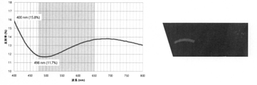
高分子フィルムとして、帝人フィルムソリューション社製ポリエステルフィルム(商品名:Q65HW、基材厚50μm)を用意し、その一方の面に、前述の金属アルコキシド溶液-Aを塗布し、130℃、2分で乾燥させ金属アルコキシド層-1を形成した。この金属アルコキシド層-1上に前述のカーボンナノチューブ分散液-IIを塗布し、140℃、5分で乾燥させ導電層を形成した。カーボンナノチューブ層形成後の表面抵抗値は、1050Ω/□であった。また、導電層形成後の反射スペクトルを図2に示す。
得られた導電性テープを蒸留水に10分間浸漬したが、外観上特に変化は見られなかった。
蒸留水を含ませた綿棒で導電層面を軽くこすったが、導電層の剥離などは観察されなかった。
[Example 2]
As a polymer film, a polyester film manufactured by Teijin Film Solutions Co., Ltd. (trade name: Q65HW, substrate thickness 50 μm) was prepared, and the above-mentioned metal alkoxide solution −A was applied to one surface thereof at 130 ° C. for 2 minutes. It was dried to form the metal alkoxide layer-1. The above-mentioned carbon nanotube dispersion liquid-II was applied onto the metal alkoxide layer-1, and dried at 140 ° C. for 5 minutes to form a conductive layer. The surface resistance value after forming the carbon nanotube layer was 1050 Ω / □. Further, the reflection spectrum after forming the conductive layer is shown in FIG.
The obtained conductive tape was immersed in distilled water for 10 minutes, but no particular change was observed in appearance.
The surface of the conductive layer was lightly rubbed with a cotton swab soaked in distilled water, but no peeling of the conductive layer was observed.
[実施例3]
実施例1の金属アルコキシド層を金属アルコキシド溶液-Bに置き換えた以外は、実施例1と同様の操作を行い、導電性テープを作成した。
得られた導電性テープを蒸留水に10分間浸漬したが、外観上特に変化は見られなかった。
蒸留水を含ませた綿棒で導電層面を軽くこすったが、導電層の剥離などは観察されなかった。
[Example 3]
The same operation as in Example 1 was performed except that the metal alkoxide layer of Example 1 was replaced with the metal alkoxide solution −B, to prepare a conductive tape.
The obtained conductive tape was immersed in distilled water for 10 minutes, but no particular change was observed in appearance.
The surface of the conductive layer was lightly rubbed with a cotton swab soaked in distilled water, but no peeling of the conductive layer was observed.
[比較例1]
カーボンナノチューブ分散液をカーボンナノチューブ分散液-Iに置き換えた以外は、実施例-1と同様の操作を行い、導電性テープを作成した。
得られた導電性テープを蒸留水に浸漬、浸漬直後から導電層表面から薄膜が剥がれること確認した。
また蒸留水を含ませた綿棒で導電層を軽く擦ると、導電層が簡単に剥がれた。
[Comparative Example 1]
A conductive tape was prepared by performing the same operation as in Example 1 except that the carbon nanotube dispersion liquid was replaced with the carbon nanotube dispersion liquid-I.
The obtained conductive tape was immersed in distilled water, and it was confirmed that the thin film was peeled off from the surface of the conductive layer immediately after the immersion.
Further, when the conductive layer was lightly rubbed with a cotton swab soaked with distilled water, the conductive layer was easily peeled off.
[比較例2]
カーボンナノチューブ分散液をカーボンナノチューブ分散液-Iに置き換えた以外は、実施例-2と同様の操作を行い、導電性テープを作成した。
得られた導電性テープを蒸留水に浸漬、浸漬直後から導電層表面から薄膜が剥がれること確認した。
[Comparative Example 2]
The same operation as in Example 2 was performed except that the carbon nanotube dispersion liquid was replaced with the carbon nanotube dispersion liquid-I, to prepare a conductive tape.
The obtained conductive tape was immersed in distilled water, and it was confirmed that the thin film was peeled off from the surface of the conductive layer immediately after the immersion.
[実施例4]
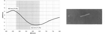
金属アルコキシド層の膜厚を変更した以外は、実施例2と同様の操作を行い、導電性テープを作成した。
高分子フィルム上に金属アルコキシド層形成後の反射スペクトルを図3、導電層形成後の反射スペクトルを図4に示す。
得られた導電性テープを蒸留水に10分間浸漬したが、外観上特に変化は見られなかった。
蒸留水を含ませた綿棒で導電層面を軽くこすったが、導電層の剥離などは観察されなかった。
得られた導電性テープの特性を表1に示す。
[Example 4]
The same operation as in Example 2 was performed except that the film thickness of the metal alkoxide layer was changed, to prepare a conductive tape.
The reflection spectrum after the formation of the metal alkoxide layer on the polymer film is shown in FIG. 3, and the reflection spectrum after the formation of the conductive layer is shown in FIG.
The obtained conductive tape was immersed in distilled water for 10 minutes, but no particular change was observed in appearance.
The surface of the conductive layer was lightly rubbed with a cotton swab soaked in distilled water, but no peeling of the conductive layer was observed.
The characteristics of the obtained conductive tape are shown in Table 1.

本発明の導電性テープは、電子顕微鏡などで連続的に薄切りされた試料をばらつきなく観察するためのキャリアテープとして好適に用いることができる。 The conductive tape of the present invention can be suitably used as a carrier tape for observing continuously sliced samples with an electron microscope or the like without variation.
Claims (10)
*が、それぞれ以下の式(1)と(2)を満足する請求項3記載の観察用導電性テープ。
-2.0< a* <0.0 (1)
2.0< b* <4.0 (2) Transmission color tones a * and b in the CIE-Lab coloring method measured from the conductive layer surface of the conductive tape.
* Is the conductive tape for observation according to claim 3, which satisfies the following formulas (1) and (2), respectively.
-2.0 <a * <0.0 (1)
2.0 <b * <4.0 (2)
Priority Applications (1)
| Application Number | Priority Date | Filing Date | Title |
|---|---|---|---|
| JP2018099787A JP7007988B2 (en) | 2018-05-24 | 2018-05-24 | Conductive tape for observation |
Applications Claiming Priority (1)
| Application Number | Priority Date | Filing Date | Title |
|---|---|---|---|
| JP2018099787A JP7007988B2 (en) | 2018-05-24 | 2018-05-24 | Conductive tape for observation |
Publications (3)
| Publication Number | Publication Date |
|---|---|
| JP2019204713A JP2019204713A (en) | 2019-11-28 |
| JP2019204713A5 JP2019204713A5 (en) | 2021-04-30 |
| JP7007988B2 true JP7007988B2 (en) | 2022-01-25 |
Family
ID=68727216
Family Applications (1)
| Application Number | Title | Priority Date | Filing Date |
|---|---|---|---|
| JP2018099787A Active JP7007988B2 (en) | 2018-05-24 | 2018-05-24 | Conductive tape for observation |
Country Status (1)
| Country | Link |
|---|---|
| JP (1) | JP7007988B2 (en) |
Citations (5)
| Publication number | Priority date | Publication date | Assignee | Title |
|---|---|---|---|---|
| JP2004028910A (en) | 2002-06-27 | 2004-01-29 | Toshiba Mach Co Ltd | Apparatus and method for preparing sliced sample |
| JP2008177143A (en) | 2006-03-28 | 2008-07-31 | Toray Ind Inc | Transparent conductive film, its manufacturing method and conductive member |
| WO2009041170A1 (en) | 2007-09-28 | 2009-04-02 | Toray Industries, Inc. | Conductive film and method for producing the same |
| JP2017181367A (en) | 2016-03-31 | 2017-10-05 | 東レ株式会社 | Conductive laminate |
| JP2018037394A (en) | 2016-08-29 | 2018-03-08 | 東レ株式会社 | Conductive laminate |
-
2018
- 2018-05-24 JP JP2018099787A patent/JP7007988B2/en active Active
Patent Citations (5)
| Publication number | Priority date | Publication date | Assignee | Title |
|---|---|---|---|---|
| JP2004028910A (en) | 2002-06-27 | 2004-01-29 | Toshiba Mach Co Ltd | Apparatus and method for preparing sliced sample |
| JP2008177143A (en) | 2006-03-28 | 2008-07-31 | Toray Ind Inc | Transparent conductive film, its manufacturing method and conductive member |
| WO2009041170A1 (en) | 2007-09-28 | 2009-04-02 | Toray Industries, Inc. | Conductive film and method for producing the same |
| JP2017181367A (en) | 2016-03-31 | 2017-10-05 | 東レ株式会社 | Conductive laminate |
| JP2018037394A (en) | 2016-08-29 | 2018-03-08 | 東レ株式会社 | Conductive laminate |
Also Published As
| Publication number | Publication date |
|---|---|
| JP2019204713A (en) | 2019-11-28 |
Similar Documents
| Publication | Publication Date | Title |
|---|---|---|
| RU2641739C2 (en) | Mixtures, methods and compositions related to conducting materials | |
| CN111621201B (en) | Metallic nanowire inks for forming transparent conductive films with fused networks | |
| JP5599462B2 (en) | Transparent conductive film containing water-soluble binder | |
| CN106205774B (en) | A kind of electrocondution slurry and transparent conducting coating | |
| AU2011220397B2 (en) | Structures with surface-embedded additives and related manufacturing methods | |
| CN106865493B (en) | Nano-structured product | |
| WO2017188175A1 (en) | Carbon nanotube dispersion, method for producing same, and conductive molded body | |
| US20150359105A1 (en) | Patterned transparent conductors and related compositions and manufacturing methods | |
| KR20040037065A (en) | Gas-barrier film and gas-barrier coating agent, and method for production thereof | |
| TW201134896A (en) | Large-area transparent conductive coatings including alloyed carbon nanotubes and nanowire composites, and methods of making the same | |
| US20220319734A1 (en) | Transparent Conductive Film | |
| US20160059605A1 (en) | Layer-by-layer assembled multilayer lamination transfer films | |
| KR20100093635A (en) | Anti-static polyester film improved coating defect and manufacturing method thereof | |
| Adhami et al. | Corrosion protection of copper by silane sol–gel coatings | |
| JP2017065964A (en) | Dispersion liquid containing carbon nanotube and conductive laminate using the same | |
| JPWO2014092142A1 (en) | Recording sheet | |
| EP3936329A1 (en) | Lamination film | |
| US10647860B2 (en) | Layered silicate/polymer composite and a method of forming the same | |
| WO2016152595A1 (en) | Far-infrared reflecting film, liquid dispersion for forming far-infrared reflecting film, method for manufacturing far-infrared reflecting film, far-infrared reflecting glass, and window | |
| JP7007988B2 (en) | Conductive tape for observation | |
| KR101534298B1 (en) | a composition for electro-magnetic interference shielding film, a method of fabricating a electro-magnetic interference shielding film therewith and an electro-magnetic interference shielding film fabricated thereby | |
| KR101328427B1 (en) | Complex conductive thin film using metal nano wire and cnt, method of manufacturing thereof | |
| JP2018202308A (en) | Silane coupling agent treatment method, production method of silane coupling agent treatment base material and production method of laminate | |
| JP6375272B2 (en) | Heat shielding material, heat insulating material, and window glass | |
| Hashizume et al. | Sol–gel titania coating on unmodified and surface-modified polyimide films |
Legal Events
| Date | Code | Title | Description |
|---|---|---|---|
| A521 | Written amendment |
Free format text: JAPANESE INTERMEDIATE CODE: A523 Effective date: 20210316 |
|
| A621 | Written request for application examination |
Free format text: JAPANESE INTERMEDIATE CODE: A621 Effective date: 20210316 |
|
| TRDD | Decision of grant or rejection written | ||
| A01 | Written decision to grant a patent or to grant a registration (utility model) |
Free format text: JAPANESE INTERMEDIATE CODE: A01 Effective date: 20211221 |
|
| A61 | First payment of annual fees (during grant procedure) |
Free format text: JAPANESE INTERMEDIATE CODE: A61 Effective date: 20220107 |
|
| R150 | Certificate of patent or registration of utility model |
Ref document number: 7007988 Country of ref document: JP Free format text: JAPANESE INTERMEDIATE CODE: R150 |