JP7002201B2 - Phase-stabilized swept-source optical coherence tomography (SS-OCT) methods and equipment including rescaling and dynamic range enhancement - Google Patents
Phase-stabilized swept-source optical coherence tomography (SS-OCT) methods and equipment including rescaling and dynamic range enhancement Download PDFInfo
- Publication number
- JP7002201B2 JP7002201B2 JP2017033430A JP2017033430A JP7002201B2 JP 7002201 B2 JP7002201 B2 JP 7002201B2 JP 2017033430 A JP2017033430 A JP 2017033430A JP 2017033430 A JP2017033430 A JP 2017033430A JP 7002201 B2 JP7002201 B2 JP 7002201B2
- Authority
- JP
- Japan
- Prior art keywords
- signal
- oct
- electrical
- detector
- electric signal
- Prior art date
- Legal status (The legal status is an assumption and is not a legal conclusion. Google has not performed a legal analysis and makes no representation as to the accuracy of the status listed.)
- Active
Links
- 0 CC1C(CC*)(*O)CCC1 Chemical compound CC1C(CC*)(*O)CCC1 0.000 description 6
- QUEBYVKXYIKVSO-UHFFFAOYSA-N CCCc1cccc(C)c1 Chemical compound CCCc1cccc(C)c1 QUEBYVKXYIKVSO-UHFFFAOYSA-N 0.000 description 1
Images


Classifications
-
- G—PHYSICS
- G01—MEASURING; TESTING
- G01B—MEASURING LENGTH, THICKNESS OR SIMILAR LINEAR DIMENSIONS; MEASURING ANGLES; MEASURING AREAS; MEASURING IRREGULARITIES OF SURFACES OR CONTOURS
- G01B9/00—Measuring instruments characterised by the use of optical techniques
- G01B9/02—Interferometers
- G01B9/02055—Reduction or prevention of errors; Testing; Calibration
- G01B9/02075—Reduction or prevention of errors; Testing; Calibration of particular errors
- G01B9/02078—Caused by ambiguity
-
- G—PHYSICS
- G01—MEASURING; TESTING
- G01B—MEASURING LENGTH, THICKNESS OR SIMILAR LINEAR DIMENSIONS; MEASURING ANGLES; MEASURING AREAS; MEASURING IRREGULARITIES OF SURFACES OR CONTOURS
- G01B9/00—Measuring instruments characterised by the use of optical techniques
- G01B9/02—Interferometers
- G01B9/02055—Reduction or prevention of errors; Testing; Calibration
- G01B9/02062—Active error reduction, i.e. varying with time
- G01B9/02067—Active error reduction, i.e. varying with time by electronic control systems, i.e. using feedback acting on optics or light
- G01B9/02069—Synchronization of light source or manipulator and detector
-
- G—PHYSICS
- G01—MEASURING; TESTING
- G01B—MEASURING LENGTH, THICKNESS OR SIMILAR LINEAR DIMENSIONS; MEASURING ANGLES; MEASURING AREAS; MEASURING IRREGULARITIES OF SURFACES OR CONTOURS
- G01B9/00—Measuring instruments characterised by the use of optical techniques
- G01B9/02—Interferometers
- G01B9/02001—Interferometers characterised by controlling or generating intrinsic radiation properties
- G01B9/02002—Interferometers characterised by controlling or generating intrinsic radiation properties using two or more frequencies
- G01B9/02004—Interferometers characterised by controlling or generating intrinsic radiation properties using two or more frequencies using frequency scans
-
- G—PHYSICS
- G01—MEASURING; TESTING
- G01B—MEASURING LENGTH, THICKNESS OR SIMILAR LINEAR DIMENSIONS; MEASURING ANGLES; MEASURING AREAS; MEASURING IRREGULARITIES OF SURFACES OR CONTOURS
- G01B9/00—Measuring instruments characterised by the use of optical techniques
- G01B9/02—Interferometers
- G01B9/02055—Reduction or prevention of errors; Testing; Calibration
- G01B9/0207—Error reduction by correction of the measurement signal based on independently determined error sources, e.g. using a reference interferometer
-
- G—PHYSICS
- G01—MEASURING; TESTING
- G01B—MEASURING LENGTH, THICKNESS OR SIMILAR LINEAR DIMENSIONS; MEASURING ANGLES; MEASURING AREAS; MEASURING IRREGULARITIES OF SURFACES OR CONTOURS
- G01B9/00—Measuring instruments characterised by the use of optical techniques
- G01B9/02—Interferometers
- G01B9/0209—Low-coherence interferometers
- G01B9/02091—Tomographic interferometers, e.g. based on optical coherence
-
- G—PHYSICS
- G01—MEASURING; TESTING
- G01B—MEASURING LENGTH, THICKNESS OR SIMILAR LINEAR DIMENSIONS; MEASURING ANGLES; MEASURING AREAS; MEASURING IRREGULARITIES OF SURFACES OR CONTOURS
- G01B2290/00—Aspects of interferometers not specifically covered by any group under G01B9/02
- G01B2290/60—Reference interferometer, i.e. additional interferometer not interacting with object
Landscapes
- Physics & Mathematics (AREA)
- General Physics & Mathematics (AREA)
- Health & Medical Sciences (AREA)
- General Health & Medical Sciences (AREA)
- Nuclear Medicine, Radiotherapy & Molecular Imaging (AREA)
- Radiology & Medical Imaging (AREA)
- Engineering & Computer Science (AREA)
- Automation & Control Theory (AREA)
- Optics & Photonics (AREA)
- Investigating Or Analysing Materials By Optical Means (AREA)
Description
本願は、以下の出願に基づく優先権を主張し、これらの全体が参照によって本願に援用される:2016年2月24日に出願された「位相安定化スウェプトソース光コヒーレンストモグラフィ(SS-OCT)の方法及び装置」と題する米国仮特許出願第62/299,397号;2016年2月24日に出願された「ダイナミックレンジ増大を含む位相安定化スウェプトソース光コヒーレンストモグラフィ(SS-OCT)の方法及び装置」と題する米国仮特許出願第62/299,461号;2016年2月24日に出願された「リスケーリングを含む位相安定化スウェプトソース光コヒーレンストモグラフィ(SS-OCT)の方法及び装置」と題する米国仮特許出願第62/299,484号。 This application claims priorities under the following applications, all of which are incorporated herein by reference: "Phase Stabilized Swept Source Optical Coherence Tomography (SS-OCT)" filed February 24, 2016. ) Methods and Devices, US Provisional Patent Application No. 62 / 299,397; "Phase Stabilized Swept Source Optical Coherence Tomography (SS-OCT) with Increased Dynamic Range" filed February 24, 2016. US Provisional Patent Application No. 62 / 299,461; Method of Phase Stabilized Swept Source Optical Coherence Tomography (SS-OCT) Containing Rescaling, filed February 24, 2016. And Equipment, US Provisional Patent Application No. 62 / 299,484.
位相不安定性は、スウェプトソース光コヒーレンストモグラフィ(SS-OCT)システムに伴う共通の問題である。スウェプトソースOCTの位相不安定性の要因には、OCTシステム内の光源(例えば波長掃引レーザー)と電気的掃引トリガー(光源の各波長掃引期間の開始時にスキャナーを動作させるためのトリガー)との間の非同期と、アナログ-デジタル変換プロセスに内在するトリガーの不安定性とが含まれる。この問題に対処するために様々なアプローチが為されてきた。しかし、それぞれのアプローチはそれぞれの問題をはらんでいる。多くのアプローチでは、光源に同期したk-クロック(ここで、k=波数=2π/波長)を、アナログ-デジタル変換器のクロック信号として、一定の内部クロックの代わりに利用している。 Phase instability is a common problem with swept source optical coherence tomography (SS-OCT) systems. A factor in the phase instability of the Swept Source OCT is between the light source in the OCT system (eg wavelength sweep laser) and the electrical sweep trigger (trigger to operate the scanner at the beginning of each wavelength sweep period of the light source). It includes asynchronous and trigger instability inherent in the analog-to-digital conversion process. Various approaches have been taken to address this issue. However, each approach has its own problems. Many approaches use a k-clock synchronized with the light source (where k = wavenumber = 2π / wavelength) as the clock signal for the analog-to-digital converter instead of a constant internal clock.
例えば、第1のアプローチでは、OCT信号(ここで、OCT信号は、一般に、OCTシステムにおいて検出される信号(例えばインターフェログラム)を意味する。)と、レーザー掃引に同期した光学的シグネチャ信号(例えば、ファイバーブラッググレーティング(FBG)により生成されるような信号)とを、単一のアナログ-デジタルチャネルで同時に検出しデジタル化する。光学的シグネチャ信号及びk-クロック情報に基づき(例えば、k-空間内において)スペクトルを整列させることにより、位相ジッター補正が実行される。しかしながら、このアプローチによれば、OCTのそれぞれの応用のために最適な仕様のFBGを決定するという複雑な問題がある。この最適化には、中心波長、反射率(シグネチャ信号の振幅)、及びパルス幅の決定が含まれる。これは、部分的に、FBG信号が飽和しOCT画像化性能の低下させることを原因とする。更に、もし波長掃引レーザーのデバイス間のばらつきが大きい場合には、FBGの1つ以上のグループについて、その性能の最適化のためにそのようなばらつきを調整する必要がある。これは、大量生産を妨げる原因となりうる。 For example, in the first approach, an OCT signal (where the OCT signal generally means a signal detected in an OCT system (eg, an interferogram)) and an optical signature signal synchronized with laser sweep (here). For example, a signal such as that produced by Fiber Bragg Grating (FBG)) is simultaneously detected and digitized on a single analog-digital channel. Phase jitter correction is performed by aligning the spectra based on the optical signature signal and k-clock information (eg, in k-space). However, this approach has the complex problem of determining the optimal specification of FBG for each application of OCT. This optimization involves determining the center wavelength, reflectance (amplitude of the signature signal), and pulse width. This is partly due to the fact that the FBG signal is saturated and the OCT imaging performance is deteriorated. Moreover, if the variability between the devices of the wavelength sweep laser is large, it is necessary to adjust for the variability for one or more groups of FBGs in order to optimize their performance. This can be a hindrance to mass production.
同様に、第2のアプローチでは、レーザー掃引に同期したトリガー信号(例えば、FBG又は光学フィルターにより生成される)によりアナログ-デジタル変換プロセスを開始しつつ、OCT信号を単一のアナログ-デジタルチャネルでデジタル化する。このトリガー信号は、OCT信号とは別に光検出器により検出され、k-クロックに基づくOCT信号のデジタル化を開始するために用いられる。このアプローチは、OCTシステムにおける光源(例えば、波長掃引レーザー)と電気的掃引トリガーとの間の非同期に対処するものであるが、アナログ-デジタル変換プロセスに内在する不定性に対処するものではない。したがって、この不定性に起因する位相ジッターに対処することはやはり不可能である。 Similarly, the second approach initiates the analog-to-digital conversion process with a laser sweep-synchronized trigger signal (eg, generated by an FBG or optical filter) while delivering the OCT signal in a single analog-digital channel. Digitize. This trigger signal is detected by a photodetector separately from the OCT signal and is used to initiate digitization of the OCT signal based on the k-clock. This approach addresses the asynchrony between the light source (eg, wavelength sweep laser) and the electrical sweep trigger in the OCT system, but not the indeterminacy inherent in the analog-to-digital conversion process. Therefore, it is still impossible to deal with the phase jitter caused by this indefiniteness.
第3のアプローチでは、アナログ-デジタル変換器は、OCT信号とFBG信号とを並行してデジタル化するために少なくとも2つの入力チャネルを備える。すなわち、例えば、同じデータ収集ユニット上の2つの異なるチャネルにより、同じk-クロックを用いて、OCT信号と光学的シグネチャ信号とを検出しデジタル化する。OCTスペクトルの整列(例えば、チャネル1)を光学的シグネチャ信号(例えば、チャネル2)に基づき実行することで位相ジッター補正が行われる。しかし、このようなハードウェア上の付加的な要請により、このアプローチでは一般にシステムのコストが増大する。更に、(2つのチャネルシステムにおいて)2倍の量のデータを収集するため、必要な演算能力や演算時間が増大してしまう。その上、2つのチャネルを用いても信号を完全に同期させることはできず、付加的な位相ジッターが残ってしまう。その原因は、アナログ-デジタル変換を行っているときに2つのチャネルを同期できないことにある。 In a third approach, the analog-to-digital converter comprises at least two input channels for digitizing the OCT and FBG signals in parallel. That is, for example, the OCT signal and the optical signature signal are detected and digitized using the same k-clock by two different channels on the same data acquisition unit. Phase jitter correction is performed by performing OCT spectrum alignment (eg, channel 1) based on an optical signature signal (eg, channel 2). However, these additional hardware requirements generally increase the cost of the system with this approach. In addition, it collects twice as much data (in two channel systems), which increases the required computing power and time. Moreover, the signals cannot be perfectly synchronized using the two channels, leaving additional phase jitter. The reason is that the two channels cannot be synchronized when performing analog-to-digital conversion.
ここで説明される第1の例によれば、光コヒーレンストモグラフィ(OCT)システムは、電気的OCT信号を出力する検出器と、アナログ-デジタル変換器と、電気信号ミキサーとを含み、前記電気信号ミキサーは、第1電気信号を第1入力にて受け、前記検出器からの前記電気的OCT信号を第2入力にて受け、前記アナログ-デジタル変換器に出力信号を出力し、前記出力信号は、前記第1電気信号及び前記電気的OCT信号の双方の電気的に混合された結合である。 According to the first example described herein, an optical coherent stromography (OCT) system comprises a detector that outputs an electrical OCT signal, an analog-digital converter, and an electrical signal mixer, said electric. The signal mixer receives the first electric signal at the first input, receives the electric OCT signal from the detector at the second input, outputs an output signal to the analog-digital converter, and outputs the output signal. Is an electrically mixed coupling of both the first electrical signal and the electrical OCT signal.
第1の例の様々な実施形態において、以下のいずれかを適用することができる。前記第1電気信号は、光信号を検出する第2検出器により生成された電気的シグネチャ信号である。前記第2検出器は、ファイバーブラッググレーティングからの前記光信号を検出し、前記第1電気信号は、前記ファイバーブラッググレーティングからの前記光信号に基づく。前記第1電気信号は、当該OCTシステムの光源掃引の同期情報を伝達する。前記電気信号ミキサーは、前記第1入力及び前記第2入力の少なくとも一方に作動的に接続された時間遅延線を含み、前記第1電気信号及び前記電気的OCT信号の少なくとも一方は、混合される前に時間遅延される。前記時間遅延線は、前記第1電気信号のパルス幅と遅延の量とを調整する。前記時間遅延は、それぞれのAスキャンについて動的に調整可能である。前記電気信号ミキサーは、前記第1入力及び前記第2入力の少なくとも一方に作動的に接続されたフィルターを更に含み、前記第1電気信号及び前記電気的OCT信号の少なくとも一方は、混合される前にフィルター処理される。前記電気信号ミキサーは、前記第1入力及び前記第2入力の少なくとも一方に作動的に接続された増幅器を更に含み、前記第1電気信号及び前記電気的OCT信号の少なくとも一方は、混合される前に増幅される。前記第1電気信号のパルス幅は、当該OCTシステムのk-クロック又は前記アナログ-デジタル変換器のクロックに相関している。前記第1電気信号は、当該OCTシステムの光源掃引の非線形性の情報を含む干渉信号に基づき生成されたリスケーリング信号である。前記干渉信号は、2つのミラー、ガラスプレートの2つの表面、又は、マッハ-ツェンダー干渉計によって生成される。k-クロックを利用しない。前記電気信号ミキサーは、更に、第2電気信号を第3入力にて受け、前記出力信号は、前記第1電気信号、前記第2電気信号、及び前記電気的OCT信号の電気的に混合された結合であり、前記第1電気信号はシグネチャ信号であり、前記第2電気信号はリスケーリング信号である。 In various embodiments of the first example, any of the following can be applied: The first electrical signal is an electrical signature signal generated by a second detector that detects an optical signal. The second detector detects the optical signal from the fiber Bragg grating, and the first electrical signal is based on the optical signal from the fiber Bragg grating. The first electric signal transmits synchronization information of the light source sweep of the OCT system. The electrical signal mixer includes a time delay line operatively connected to at least one of the first input and the second input, and at least one of the first electrical signal and the electrical OCT signal is mixed. Time delayed before. The time delay line adjusts the pulse width and the amount of delay of the first electric signal. The time delay can be dynamically adjusted for each A scan. The electrical signal mixer further includes a filter operatively connected to at least one of the first input and the second input, and at least one of the first electrical signal and the electrical OCT signal is before being mixed. Is filtered to. The electrical signal mixer further includes an amplifier operatively connected to at least one of the first input and the second input, and at least one of the first electrical signal and the electrical OCT signal is before being mixed. Is amplified to. The pulse width of the first electrical signal correlates with the k-clock of the OCT system or the clock of the analog-to-digital converter. The first electric signal is a rescaling signal generated based on an interference signal including information on the non-linearity of the light source sweep of the OCT system. The interference signal is generated by two mirrors, two surfaces of a glass plate, or a Mach-Zehnder interferometer. Do not use the k-clock. The electric signal mixer further receives a second electric signal at the third input, and the output signal is electrically mixed with the first electric signal, the second electric signal, and the electric OCT signal. It is a coupling, the first electrical signal is a signature signal, and the second electrical signal is a rescaling signal.
第2の例によれば、光コヒーレンストモグラフィ(OCT)システムを用いて画像化を行う方法は、第1電気信号を生成し、検出器により電気的OCT信号を生成し、電気信号ミキサーにより前記第1電気信号と前記電気的OCT信号とを電気的に混合し、前記電気的に混合された前記第1電気信号及び前記電気的OCT信号を含む出力信号を生成し、前記電気信号ミキサーは、前記第1電気信号を第1入力にて受け、前記検出器からの前記電気的OCT信号を第2入力にて受け、アナログ-デジタル変換器に前記出力信号を出力する。 According to the second example, the method of imaging using an optical coherence stromography (OCT) system produces a first electrical signal, an electrical OCT signal by a detector, and the electrical signal mixer described above. The electric signal mixer electrically mixes the first electric signal and the electric OCT signal to generate an output signal including the electrically mixed first electric signal and the electric OCT signal. The first electric signal is received at the first input, the electric OCT signal from the detector is received at the second input, and the output signal is output to the analog-digital converter.
第2の例の様々な実施形態において、以下のいずれかを適用することができる。前記第1電気信号は、光信号を検出する検出器により生成されたシグネチャ信号である。前記検出器は、ファイバーブラッググレーティングからの前記光信号を検出し、前記第1電気信号は、前記ファイバーブラッググレーティングからの前記光信号に基づく。前記第1電気信号は、当該OCTシステムの光源掃引の同期情報を伝達する。混合よりも前に、前記第1電気信号及び前記電気的OCT信号の少なくとも一方に時間遅延を導入する。更に、時間遅延を導入し、前記第1電気信号のパルス幅を調整する。前記時間遅延は、それぞれのAスキャンについて動的に調整可能である。更に、混合よりも前に、前記第1電気信号及び前記電気的OCT信号の少なくとも一方をフィルター処理する。更に、混合よりも前に、前記第1電気信号及び前記電気的OCT信号の少なくとも一方を増幅する。前記第1電気信号のパルス幅は、当該OCTシステムのk-クロック又は前記アナログ-デジタル変換器のクロックに相関している。前記第1電気信号は、当該OCTシステムの光源掃引の非線形性の情報を含む干渉信号に基づき生成されたリスケーリング信号である。前記干渉信号は、2つのミラー、ガラスプレートの2つの表面、又は、マッハ-ツェンダー干渉計によって生成される。更に、第2電気信号を生成し、前記第1電気信号、前記第2電気信号、及び前記電気的OCT信号を、前記電気信号ミキサーにより電気的に混合し、生成された前記出力信号は、電気的に混合された前記第1電気信号、前記第2電気信号、及び前記電気的OCT信号を含み、前記第1電気信号はシグネチャ信号であり、前記第2電気信号はリスケーリング信号である。更に、アナログ-デジタル変換よりも前に、前記出力信号又は前記電気的OCT信号の受動的電気的減衰により当該OCTシステムのダイナミックレンジを調整する。前記受動的電気的減衰は、受動的電気的アッテネーター、又は前記検出器のゲインの最適化によって得られる。前記検出器のゲインの最適化は、当該OCTシステムのノイズ解析に基づく。 In various embodiments of the second example, any of the following can be applied: The first electric signal is a signature signal generated by a detector that detects an optical signal. The detector detects the optical signal from the fiber Bragg grating, and the first electrical signal is based on the optical signal from the Fiber Bragg grating. The first electric signal transmits synchronization information of the light source sweep of the OCT system. Prior to mixing, a time delay is introduced in at least one of the first electrical signal and the electrical OCT signal. Further, a time delay is introduced to adjust the pulse width of the first electric signal. The time delay can be dynamically adjusted for each A scan. Further, prior to mixing, at least one of the first electrical signal and the electrical OCT signal is filtered. Further, prior to mixing, at least one of the first electrical signal and the electrical OCT signal is amplified. The pulse width of the first electrical signal correlates with the k-clock of the OCT system or the clock of the analog-to-digital converter. The first electric signal is a rescaling signal generated based on an interference signal including information on the non-linearity of the light source sweep of the OCT system. The interference signal is generated by two mirrors, two surfaces of a glass plate, or a Mach-Zehnder interferometer. Further, a second electric signal is generated, the first electric signal, the second electric signal, and the electric OCT signal are electrically mixed by the electric signal mixer, and the generated output signal is electric. The first electrical signal includes the first electrical signal, the second electrical signal, and the electrical OCT signal that are mixed with each other, the first electrical signal is a signature signal, and the second electrical signal is a rescaling signal. Further, prior to the analog-to-digital conversion, the dynamic range of the OCT system is adjusted by the passive electrical attenuation of the output signal or the electrical OCT signal. The passive electrical attenuation is obtained by a passive electrical attenuator, or by optimizing the gain of the detector. The optimization of the detector gain is based on the noise analysis of the OCT system.
第3の例によれば、光コヒーレンストモグラフィ(OCT)システムを用いて画像化を行う方法は、検出器により電気的OCT信号を生成し、アナログ-デジタル変換よりも前に、前記電気的OCT信号の受動的電気的減衰により当該OCTシステムのダイナミックレンジを調整する。 According to a third example, the method of imaging using an optical coherence tomography (OCT) system produces an electrical OCT signal by a detector, said electrical OCT prior to analog-digital conversion. The dynamic range of the OCT system is adjusted by the passive electrical attenuation of the signal.
第3の例の様々な実施形態において、以下のいずれかを適用することができる。前記受動的電気的減衰は、受動的電気的アッテネーター、又は前記検出器のゲインの最適化によって得られる。当該OCTシステムのノイズを解析し、前記検出器のゲインの最適化は、当該ノイズ解析に基づく。 In various embodiments of the third example, any of the following can be applied: The passive electrical attenuation is obtained by a passive electrical attenuator, or by optimizing the gain of the detector. The noise of the OCT system is analyzed, and the optimization of the gain of the detector is based on the noise analysis.
本開示は、OCTシステムにおける前述した位相ジッターの問題に対処することが可能であり、且つ、前述した現在の方法の限界を克服することが可能な方法及び装置に関する。簡単に言えば、シグネチャ信号及び/又はリスケーリング信号をOCT信号に電気的に合成するために電気信号ミキサーが利用される。光学的な実施形態よりむしろ、これら信号の電気的な実施形態を組み合わせることにより、合成よりも前にこれら信号を個別に処理してもよい。例えば、これら信号を増幅したり、フィルター処理したりしてよく、また、ユーザ定義の時間遅延により誘導されてもよい。このようにして、結果として得られる混合された信号を、例えば、より容易に識別でき、Aスキャンの整列のためにより良く利用することができる。更に、付加的な信号(例えば、シグネチャ信号及びリスケーリング信号)によるノイズが混入しにくくなり、さもなければ付加的な信号がOCT信号に干渉しにくくなる。 The present disclosure relates to methods and devices capable of addressing the aforementioned phase jitter problems in OCT systems and overcoming the limitations of the aforementioned current methods. Simply put, an electrical signal mixer is used to electrically synthesize a signature signal and / or a rescaling signal into an OCT signal. These signals may be processed individually prior to synthesis by combining electrical embodiments of these signals rather than optical embodiments. For example, these signals may be amplified, filtered, or induced by a user-defined time delay. In this way, the resulting mixed signal can be more easily identified, for example, and better utilized for A-scan alignment. Further, noise due to additional signals (eg, signature signals and rescaling signals) is less likely to be mixed in, otherwise the additional signals are less likely to interfere with the OCT signal.
より具体的には、OCTシステムに電気信号ミキサーを設けることによって位相安定化が達成される。図1に示すように、OCTシステムの部分として考えられる光検出器により、OCTインターフェログラム信号とシグネチャ信号(例えば、ファイバーブラッググレーティングからのシグネチャ信号)とが検出される(106、108)。電気信号ミキサー100は、OCTインターフェログラム102とシグネチャ信号104とを電子的に合成する。任意的ではあるが、OCTインターフェログラム102及びシグネチャ信号104に対して独立に時間遅延を与えてもよい(110、112)。例えば、或る実施形態において、シグネチャ信号104のみに時間遅延112を導入してもよい。
More specifically, phase stabilization is achieved by providing an electrical signal mixer in the OCT system. As shown in FIG. 1, a photodetector considered as part of an OCT system detects an OCT interferogram signal and a signature signal (eg, a signature signal from a fiber Bragg grating) (106, 108). The
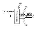
この電気的な合成の単純化された概略図を図2Aに示し、他のアプローチにおいて使用される光学的な合成の概略図を図2Bに示す。図2Aにおいて、それぞれ検出されて電気信号に変換された後にこれら信号が合成されるが、図2Bでは、光学的な実施形態のこれら信号が単一の光検出器によって検出され、それから単一の電気信号が出力される。ここで、バランス検出器204よりも前において光学的OCT信号202に光学的に結合されるファイバーブラッググレーティング200により生成された光学的FBG信号をFBGoで示す。また、光検出器204により検出された後に出力される電気的OCT信号208に電気的に合成される電気的FBG信号(例えば、FBGo信号を検出する光検出器により出力される電気的FBG信号)をFBGeで示す。
A simplified schematic of this electrical synthesis is shown in FIG. 2A and a schematic of the optical synthesis used in other approaches is shown in FIG. 2B. In FIG. 2A, these signals are combined after being detected and converted into electrical signals, respectively, whereas in FIG. 2B, these signals of the optical embodiment are detected by a single photodetector and then a single. An electric signal is output. Here, the optical FBG signal generated by the fiber Bragg grating 200 optically coupled to the optical OCT signal 202 prior to the
図1の参照に戻る。結果として得られる信号は、次に、単一チャネルのアナログ-デジタル変換器によってデジタル化される(114)。続いて、(例えば、後処理において)軸スキャン(Aスキャン)の集合をそれぞれのAスキャンにおけるFBG信号に基づき数値的に整列することによって(116)、OCT位相安定化を達成することができる。最後に、これらAスキャンのフーリエ変換を介して、インターフェログラムを、深さ情報を有するOCTデータに変換することができる(118)。このようにして、干渉することのない、さもなければOCT信号内のデータを変化させないように、カスタマイズされたFBG信号を適用することができる。よって、Aスキャンを整列させるときの参照としてFBG信号をより容易に且つ好適に利用することができる。カスタマイズされたFBG信号の例として、パルス幅、振幅、時間遅延、及び、他の類似の電気信号の特性がある。或るいくつかの実施形態において、パルス幅が、OCTシステムのk-クロックに相関していてもよい。 Return to reference in FIG. The resulting signal is then digitized by a single channel analog-to-digital converter (114). Subsequently, OCT phase stabilization can be achieved (116) by numerically aligning the set of axis scans (A scans) based on the FBG signal in each A scan (eg, in post-processing). Finally, through these A-scan Fourier transforms, the interferogram can be transformed into OCT data with depth information (118). In this way, a customized FBG signal can be applied so as not to interfere or otherwise change the data in the OCT signal. Therefore, the FBG signal can be more easily and suitably used as a reference when aligning the A scan. Examples of customized FBG signals are pulse width, amplitude, time delay, and other similar electrical signal characteristics. In some embodiments, the pulse width may correlate with the k-clock of the OCT system.
FBG信号はここに説明されているが、任意の信号を同じ要領で用いることができ、そのような信号、又は、そのような信号の一部が、光源(例えば、レーザー)の掃引の同期情報を伝達するものであればよい。更に、レーザー掃引の同期情報を伝達する光学的/電気的信号(又は、その一部)から、そのような信号(又は、そのような信号の一部)を得るようにしてもよい。そのような信号は、例えば、スパイクパルス、矩形、正弦波形などであってよく、また、任意の周波数で発生してもよい。更に、前述したAスキャンの数値的な整列は、任意の数値的方法に基づいていてよい。例えば、ピーク検出、相関に基づくアルゴリズム、及び/又は、OCT信号に合成されデジタル化されるシグネチャ信号のカスタマイズされた形状に対し最適に作用するようにカスタマイズされたアルゴリズムがある。 Although FBG signals are described herein, any signal can be used in the same manner, and such a signal, or part of such a signal, is the synchronization information of the sweep of a light source (eg, a laser). Anything that conveys. Further, such a signal (or a part of such a signal) may be obtained from an optical / electrical signal (or a part thereof) that transmits the synchronization information of the laser sweep. Such signals may be, for example, spike pulses, rectangles, sinusoidal waveforms, etc., and may be generated at any frequency. Further, the numerical alignment of the A scan described above may be based on any numerical method. For example, there are peak detection, correlation-based algorithms, and / or algorithms customized to work optimally on the customized shape of the signature signal that is synthesized and digitized into the OCT signal.
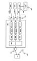
前述した例の構造的な概略図を図3に示す。この例によれば、OCT信号は、光検出器300によって検出され、電気信号ミキサー318の第1入力チャネル302に電気的OCT信号として入力される。同様に、FBG信号は、他の光検出器304により検出され、電気信号ミキサー318の第2入力チャネル306に電気的シグネチャ信号として入力される。第1及び第2入力チャネル302、306にそれぞれ対応するプログラマブル時間遅延線308、310は、対応する信号にユーザ定義の時間遅延量を導入する。これら2つの信号は、アナログ信号ミキサー312により加算され、出力チャネル314を介して出力される。そして、この出力信号は、データ収集ユニット316内のアナログ-デジタル変換器によってデジタル化される。
FIG. 3 shows a structural schematic diagram of the above-mentioned example. According to this example, the OCT signal is detected by the
第2の実施形態を図4に示す。この実施形態によれば、電気信号ミキサー412は、3つ以上の入力チャネルを含む。例えば、第3光検出器400により検出された第2FBG信号のための入力チャネル402が付加される。任意的ではあるが、電気信号ミキサー412は、前述した時間遅延408を付加することに加えて、信号の混合よりも前に、入力信号にフィルター処理を施すためのフィルター404、及び/又は、入力信号を増幅するための増幅器406を含んでいてもよい。フィルター404は、ローパス、ハイパス、及びバンドパスを含む、任意の種類であってよい。フィルター404は、アナログでもデジタルでもよい。同様に、任意の増幅器406を用いてよく、また、増幅器406はアナログでもデジタルでもよい。なお、前述した遅延についても任意的である。フィルター404、遅延線408、及び増幅器406は、それぞれの入力チャネルからのそれぞれの信号について同じでもよいし、それぞれの入力チャネルからのそれぞれの信号ごとに個別であってもよい。換言すると、それぞれの入力信号の処理を独立に行ってもよい。
The second embodiment is shown in FIG. According to this embodiment, the
3つ以上の入力チャネルを有する電気信号ミキサー412について図4ではフィルター404及び増幅器406が示されているが、例えば図3の実施形態に示すように2つの入力チャネルを有する電気信号ミキサー318に、これら特徴を組み込むことも可能である。そして、全ての入力信号がミキサー410により電気的に合成され、図3に関する前述の場合と同様に、出力チャネル414からデータ収集ユニット316に出力される。他の実施形態において、ミキサー312、410により出力される合成出力信号に、フィルター処理、増幅処理、及び遅延処理を付加的又は代替的に適用することができる。
For an
電気信号ミキサー318、412のミキサー312、410の例示的な実施形態についての同等な電気的概略図を図5及び図6に示す。なお、図5及び図6は、例示的な概略を示すものに過ぎず、限定を意図するものではない。むしろ、ここに示されて説明されるミキサーの特徴を、様々な変形において実施することが可能である。
Equivalent electrical schematics for exemplary embodiments of
図5に示すミキサー500によれば、RC回路R3及びC1(502)と、RC回路R4及びC2(504)が、DC信号を遮断し、短絡を防止する。RC回路502、504は、RC回路の時定数に基づいて時間遅延を誘導してもよい。所望の時定数、DCレベルなどに応じた抵抗や静電容量の値に基づいて、RC回路502、504の構成要素を選択してもよい。また、RC回路502、504の構成要素は、可変抵抗器、可変コンデンサーなどを用いて動的にプログラム可能であってもよい。RC回路502、504は、同じ構成でもよいし、対応する入力信号に応じて異なった構成でもよい。そして、これら2つの入力信号はオペアンプ506の非反転端子にて合成され、その出力信号がオペアンプ506から出力される。
According to the
同様に、図6に示すミキサー600によれば、C5及びR5(602)とC5及びR6(604)との加算が、それぞれ、付加的に入力信号にフィルター処理を施す。類似の同等な回路を適用することももちろん可能である。なお、ミキサー500、600内の時間遅延及びフィルターは、図3及び図4に示すフィルター404、増幅器406、及び遅延線308、310、408に付加される。
Similarly, according to the
図7A及び図7Bは、信号の光学的合成を利用した他のアプローチに関する前述した方法を概念的に示す。図7Aから分かるように、(矢印で示す)FBGo信号が光学的OCT信号と光学的に合成される場合、掃引範囲の変動により、結果として得られる信号内のFBG信号が「なくなる」。換言すると、FBGo信号は、多くの光学的OCT信号も生成されるときに生成される。よって、OCT信号からFBG信号を容易に識別することができず、Aスキャンを整列するときにFBG信号の位置を特定することが困難になるおそれがある。更に、光学的OCT信号に対するFBGo信号の導入は、それ自身のアーティファクトを、結果として得られる信号に引き起こす。よって、たとえこのアーティファクトを除去したり処理したりしても、画像の質が低下する可能性がある。 7A and 7B conceptually show the aforementioned methods for other approaches utilizing optical synthesis of signals. As can be seen from FIG. 7A, when the FBGo signal (indicated by the arrow) is optically combined with the optical OCT signal, the variation in the sweep range "eliminates" the FBG signal in the resulting signal. In other words, the FBGo signal is generated when many optical OCT signals are also generated. Therefore, the FBG signal cannot be easily identified from the OCT signal, and it may be difficult to specify the position of the FBG signal when aligning the A scans. Moreover, the introduction of the FBGo signal to the optical OCT signal causes its own artifacts in the resulting signal. Therefore, even if this artifact is removed or processed, the quality of the image may be degraded.
逆に、図7Bに示すように、(同じく矢印で示す)FBGe信号が時間遅延され電気的OCT信号と電子的に合成される場合、FBGe信号はより一層識別可能であり、結果として得られるOCT信号と干渉しない。換言すると、電気的OCT信号と合成されるときにOCT信号データの外部にFBGe信号が存在するように、FBGe信号に時間遅延を与えることができる。したがって、FBGe信号は、検出されたいずれのデータとも干渉せず、また、それを劣化させることもない。図7Bは、OCT信号よりも後のFBGe信号を示す。他の実施形態において、OCT信号よりも前にFBGe信号を発生するようにOCT信号に時間遅延を施してもよい。 Conversely, as shown in FIG. 7B, if the FBGe signal (also indicated by an arrow) is time-delayed and electronically combined with an electrical OCT signal, the FBGe signal is even more identifiable and the resulting OCT. Does not interfere with the signal. In other words, the FBGe signal can be time-delayed so that the FBGe signal is outside the OCT signal data when combined with the electrical OCT signal. Therefore, the FBGe signal does not interfere with any of the detected data and does not degrade it. FIG. 7B shows the FBGe signal after the OCT signal. In other embodiments, the OCT signal may be time-delayed to generate the FBGe signal prior to the OCT signal.
図8及び図9は、電気信号ミキサーに入力される信号(例えば、FBG信号)に時間遅延を誘導するための電気信号ミキサーの時間遅延線の例示的な実施形態を示す。例えば、図8は、単安定マルチバイブレーターに基づく遅延のブロック図、及び、各ステップでの信号の変化の対応する可視化を示す。図8に示す実施形態によれば、2μs信号がFBGe信号に付加される。次に、この信号が反転され、10ns信号が付加される。これにより、パルス幅10nsを有する2μsだけ遅延されたFBGe信号が生成される。使用されるマルチバイブレーターを変更することで、遅延及びパルス幅を調整してもよい。パルス幅は、アナログ-デジタル変換器のクロック又はk-クロックに相関していてよい。更に、それぞれのAスキャンについて時間遅延の量が固定されている必要はない。むしろ、それぞれのAスキャンについて、時間遅延の量を動的に調整することができる。 8 and 9 show an exemplary embodiment of a time delay line of an electrical signal mixer for inducing a time delay in a signal (eg, an FBG signal) input to the electrical signal mixer. For example, FIG. 8 shows a block diagram of the delay based on a monostable multivibrator and a corresponding visualization of signal changes at each step. According to the embodiment shown in FIG. 8, a 2 μs signal is added to the FBGe signal. Next, this signal is inverted and a 10 ns signal is added. This produces an FBGe signal delayed by 2 μs with a pulse width of 10 ns. The delay and pulse width may be adjusted by changing the multivibrator used. The pulse width may correlate with the clock or k-clock of the analog-to-digital converter. Furthermore, the amount of time delay need not be fixed for each A scan. Rather, the amount of time delay can be dynamically adjusted for each A scan.
図9に示す実施形態は、10ビットダウンカウンターを用いたカウンターベースの遅延を利用している。なお、アップカウンターを用いることも可能である。また、任意の電子的時間遅延線を用いることもでき、更に、そのような遅延の量はユーザ定義されてもプログラム可能でもよい。例えば、遅延の量は、使用される構成要素によって選択可能であってよく、また、マイクロプロセッサーを介してデジタル的に制御されてもよい。上記の例に加えて、時間遅延線は、単純な電気ケーブル、フィールドプログラマブルゲートアレイ(FPGA)ベースの回路基板、デジタル信号処理ベースの回路基板、又は、他の類似のプロセッサー及びハードウェアを用いてそのように実装してもよい。 The embodiment shown in FIG. 9 utilizes a counter-based delay with a 10-bit down counter. It is also possible to use an up counter. Also, any electronic time delay line can be used, and the amount of such delay may be user-defined or programmable. For example, the amount of delay may be selectable depending on the components used and may be digitally controlled via a microprocessor. In addition to the above example, the time delay line may use a simple electrical cable, a field programmable gate array (FPGA) based circuit board, a digital signal processing based circuit board, or other similar processors and hardware. It may be implemented as such.
図10に示すように、電気信号ミキサー1000は、付加的な入力チャネル1002にて電気的リスケーリング信号を受信する。このリスケーリング信号は、リスケーリングのための干渉信号を受ける検出器1006により出力される。この干渉信号は、例えば、マッハ-ツェンダー干渉計1008、2つのミラー、又は、ガラスプレートの2つの表面によって生成されてよく、又は、相対的な位相シフトを決定できる類似のデバイスによって生成されてもよい。FBGe信号及び電気的OCT信号と同様に、前述したように、リスケーリング信号にフィルター処理を施したり、リスケーリング信号を増幅したり、リスケーリング信号に置換遅延を与えたりしてよい。そして、この信号と、電気信号ミキサー1000の他のチャネルにて入力されたFBGe信号及び電気的OCT信号とを電気的に混合し、前述した要領で出力チャネル1014から出力することができる。
As shown in FIG. 10, the
図10に示す実施形態においては、アナログ-デジタル変換/デジタル化を行うために、アナログ-デジタル変換器の内部クロック1006がk-クロックの代わりに設けられる。このような実施形態によれば、k-クロックを用いることなくOCTシステムを動作させることができる。このようにして、例えば、2つのミラー又はガラスプレートの2つの表面により生成された干渉信号のような、よりクリーンでレーザー掃引の非線形性の情報を伝達する信号を、OCT信号に合成することができる。そうすることで、k-クロックを用いる必要がなくなる。k-クロックを必要とすることなく、固定周波数の内部クロックをデジタル化のために利用することができる。これにより、システムのコストを低減でき、及び/又は、システム設計のフレキシビリティを促進することができる。
In the embodiment shown in FIG. 10, an
リスケーリングのために、更に、掃引の非線形性がOCTイメージングに及ぼす影響を抑制するために、そのような干渉信号を使用することも可能である。なお、そのようなコンセプトを、位相ジッター補正の促進及び/又は位相曖昧性(phase ambiguity)の除去のために検討される位相ジッター補正方法に組み合わせることができる。 It is also possible to use such interference signals for rescaling and to suppress the effect of sweep non-linearity on OCT imaging. It should be noted that such a concept can be combined with a phase jitter correction method considered for facilitating phase jitter correction and / or removing phase ambiguity.
図示は省略するが、電気信号ミキサーからの出力信号を受信するデータ収集ユニットは、更に、後処理用のマイクロプロセッサー(例えば、信号処理プロセッサー)に接続されていてよい。例えば、この後処理は、前述したAスキャンの整列、更なるフィルター処理信号、Bスキャン、Cスキャン、正面画像の生成、画像のセグメンテーションなどを含んでよい。 Although not shown, the data acquisition unit that receives the output signal from the electric signal mixer may be further connected to a microprocessor for post-processing (for example, a signal processing processor). For example, this post-processing may include the aforementioned A-scan alignment, further filtered signals, B-scan, C-scan, frontal image generation, image segmentation, and the like.
ここに説明される他の態様によれば、アナログ-デジタル変換よりも前に受動的電気的減衰を適用することで、OCTシステムのダイナミックレンジ(分光器を用いたスペクトラルドメインOCT及びスウェプトソースOCTの双方を含む)を調整することができる。そのような特性により、必ずしも感度の妥協を伴うことなく、画像化システムのダイナミックレンジを最適化することが可能となる。受動的電気的アッテネーター(減衰器)及び/又はOCTシステムの光検出器のゲインの最適化によって、受動的電気的減衰を実現することができる。そのような最適化は、ショットノイズ、相対強度ノイズ、センサーノイズ、及びアナログ-デジタルデジタル化ノイズを含む、システムのノイズ解析に基づくものであってよい。受動的減衰は、減衰された信号の信号対ノイズ比に影響を及ぼすことなく、少なくとも15dBに至るまで実施することができる。そのような受動的減衰は、例えば、眼の前眼部/角膜のOCTイメージングに適用可能である。ここで、角膜頂点からの反射は非常に強く、典型的には光検出器を飽和させ、アーティファクトを生ずる。受動的電気的減衰により、信号対ノイズ比の妥協を伴うことなく、この反射の影響を軽減することが可能である。 According to another aspect described herein, by applying passive electrical attenuation prior to analog-to-digital conversion, the dynamic range of the OCT system (spectral domain OCT using a spectroscope and swept source OCT). (Including both) can be adjusted. Such characteristics make it possible to optimize the dynamic range of the imaging system without necessarily compromising sensitivity. Passive electrical attenuation can be achieved by optimizing the gain of the passive electrical attenuator and / or the photodetector of the OCT system. Such optimization may be based on system noise analysis, including shot noise, relative intensity noise, sensor noise, and analog-digital digitization noise. Passive attenuation can be performed up to at least 15 dB without affecting the signal-to-noise ratio of the attenuated signal. Such passive attenuation is applicable, for example, to OCT imaging of the anterior segment of the eye / cornea. Here, the reflections from the apex of the cornea are very strong, typically saturate the photodetector and produce artifacts. Passive electrical attenuation can mitigate the effects of this reflection without compromising the signal-to-noise ratio.
ここで、受動的減衰は、電気的OCT信号に適用可能であり、例えば、電気的シグネチャ信号(例えば、FBG信号)との混合より前の増幅器406による電気信号の混合において適用可能である。他の実施形態において、データ収集ユニットによる収集より前の合成された出力信号に、受動的減衰を適用してもよい。この減衰は、ディスクリート電子部品、プロセッサー等の集積回路などを用いて実現可能である。
Here, passive attenuation is applicable to electrical OCT signals, for example in mixing electrical signals by
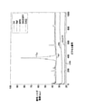
図11A及び図11Bは、それぞれ、受動的減衰8dB及び受動的減衰15dBの場合における様々な信号のノイズレベルを示す。同図から分かるように、X軸は、サンプル画像のピクセル番号を表し、Y軸は、OCTシステムからの信号又はノイズの強度を表す。図示された信号/ノイズは、干渉信号からのもの(Int)、サンプルからの信号が遮断されたときの参照信号のノイズフロア(Ref)、バランス検出器が光を検出していないときの熱ノイズフロア(BPD)、データ収集ユニットに接続されたシングルエンド差動変換器(one single-ended-to-differential converter)のノイズフロア(SE2DIFF)、及び、データ収集ユニットに入力がないときのデータ収集ノイズフロア(DAQ)を含む。図11A及び図11Bを比較すると、減衰を8dBから15dBに増加させることで、BPD及びDAQのノイズフロアの間の相違を減少できることが分かる。換言すると、ここで、前述した受動的減衰により、OCTシステムのダイナミックレンジを増大することができる。 11A and 11B show the noise levels of the various signals in the case of passive attenuation 8 dB and passive attenuation 15 dB, respectively. As can be seen from the figure, the X-axis represents the pixel number of the sample image and the Y-axis represents the intensity of the signal or noise from the OCT system. The signal / noise shown is from the interference signal (Int), the noise floor of the reference signal when the signal from the sample is blocked (Ref), and the thermal noise when the balance detector is not detecting light. The noise floor (SE2DIFF) of the floor (BPD), the noise floor (SE2DIFF) of the single-ended differential converter connected to the data collection unit, and the data collection noise when there is no input to the data collection unit. Includes floor (DAQ). Comparing FIGS. 11A and 11B, it can be seen that increasing the attenuation from 8 dB to 15 dB can reduce the difference between the BPD and DAQ noise floors. In other words, here, the passive attenuation described above can increase the dynamic range of the OCT system.
ここに説明された様々な実施形態は、OCTシステムから得られる眼の画像データを参照できる。しかしながら、例えば超音波のように、眼以外の対象に関する画像データを得るための、他のタイプのイメージング装置を用いて取得された画像データに対し、本開示に係る技術及び処理を同様に適用してもよい。 The various embodiments described herein can refer to image data of the eye obtained from the OCT system. However, the techniques and processes according to the present disclosure are similarly applied to image data acquired using other types of imaging devices for obtaining image data relating to objects other than the eye, such as ultrasound. You may.
また、プロセッサーによりハードウェア及び/又はソフトウェアを介して自動的に上記の態様、実施形態、及び例を実施するようにしてもよい。ここに使用される「プロセッサー」は、任意個数の電気部品(例えば、抵抗器、トランジスター、コンデンサー、インダクターなどを含む)を含む任意の電気回路(又は、その部分)を指す。この回路は、例えば、集積回路、集積回路のセット、マイクロコントローラー、マイクロプロセッサー、プリント回路基板(PCB)等に設けられたディスクリート電子部品の集まりを含む、任意の形態の回路であってよい。プロセッサーは、ランダムアクセスメモリー、フラッシュメモリー、デジタルハードディスクなどの或る形態のメモリ(揮発性又は不揮発性)に格納された命令を実行可能であってよい。プロセッサーは、スタンドアローンでも、画像データの処理以外の動作のために使用されるコンピュータの部分であってもよい。なお、以上の説明は非限定的であり、以上に説明した例は、想起される多くの適用可能なプロセッサーのうちのほんの幾つかに過ぎない。
Further, the processor may automatically implement the above embodiments, embodiments, and examples via hardware and / or software. As used herein, "processor" refers to any electrical circuit (or portion thereof) that includes any number of electrical components (including, for example, resistors, transistors, capacitors, inductors, etc.). The circuit may be of any form, including, for example, an integrated circuit, a set of integrated circuits, a microcontroller, a microprocessor, a collection of discrete electronic components provided on a printed circuit board (PCB), and the like. The processor may be capable of executing instructions stored in some form of memory (volatile or non-volatile) such as random access memory, flash memory, digital hard disk. The processor may be standalone or part of a computer used for operations other than processing image data. It should be noted that the above description is non-limiting, and the examples described above are only a few of the many applicable processors that are recalled.
Claims (11)
ファイバーブラッググレーティングからの光信号を検出する検出器により生成されるシグネチャ信号であり、当該OCTシステムの光源掃引の同期情報を伝達する第1電気信号を生成し、
検出器によりOCTインターフェログラム信号を生成し、
電気信号ミキサーにより前記第1電気信号と前記OCTインターフェログラム信号とを電気的に混合し、
前記電気的に混合された前記第1電気信号及び前記OCTインターフェログラム信号を含む出力信号を生成し、
少なくともフーリエ変換を介して前記出力信号から画像を生成し、
前記電気信号ミキサーは、前記第1電気信号を第1入力にて受け、前記検出器からの前記OCTインターフェログラム信号を第2入力にて受け、アナログ-デジタル変換器に前記出力信号を出力する、
方法。 A method of imaging using an optical coherence tomography (OCT) system.
It is a signature signal generated by a detector that detects an optical signal from a fiber Bragg grating, and generates a first electrical signal that conveys synchronization information of the light source sweep of the OCT system.
The detector generates an OCT interferogram signal and
The first electric signal and the OCT interferogram signal are electrically mixed by an electric signal mixer.
An output signal including the electrically mixed first electrical signal and the OCT interferogram signal is generated.
Generate an image from the output signal, at least via a Fourier transform,
The electric signal mixer receives the first electric signal at the first input, receives the OCT interferogram signal from the detector at the second input, and outputs the output signal to the analog-digital converter. ,
Method.
第2電気信号を生成し、
前記第1電気信号、前記第2電気信号、及び前記OCTインターフェログラム信号を、前記電気信号ミキサーにより電気的に混合し、
生成された前記出力信号は、電気的に混合された前記第1電気信号、前記第2電気信号、及び前記OCTインターフェログラム信号を含み、
前記第2電気信号はリスケーリング信号である、
請求項1から6のいずれかに記載の方法。 In addition,
Generate a second electrical signal,
The first electric signal, the second electric signal, and the OCT interferogram signal are electrically mixed by the electric signal mixer.
The generated output signal includes the electrically mixed first electrical signal, the second electrical signal, and the OCT interferogram signal.
The second electrical signal is a rescaling signal.
The method according to any one of claims 1 to 6.
前記OCTインターフェログラム信号を出力する前記検出器と、
前記電気信号ミキサーと、
前記アナログ-デジタル変換器と、
信号処理プロセッサーと
を含み、
前記電気信号ミキサーは、前記第1電気信号を第1入力にて受け、前記検出器からの前記OCTインターフェログラム信号を第2入力にて受け、前記出力信号を生成し、前記アナログ-デジタル変換器に前記出力信号を出力し、
前記信号処理プロセッサーは、前記画像の生成を行う、
OCTシステム。 An optical coherence tomography (OCT) system for performing the method according to any one of claims 1 to 10.
The detector that outputs the OCT interferogram signal and
With the electric signal mixer
With the analog-to-digital converter
Including signal processing processor
The electric signal mixer receives the first electric signal at the first input, receives the OCT interferogram signal from the detector at the second input, generates the output signal, and performs the analog-to-digital conversion. The output signal is output to the device,
The signal processor generates the image.
OCT system.
Applications Claiming Priority (8)
| Application Number | Priority Date | Filing Date | Title |
|---|---|---|---|
| US201662299461P | 2016-02-24 | 2016-02-24 | |
| US201662299397P | 2016-02-24 | 2016-02-24 | |
| US201662299484P | 2016-02-24 | 2016-02-24 | |
| US62/299,397 | 2016-02-24 | ||
| US62/299,461 | 2016-02-24 | ||
| US62/299,484 | 2016-02-24 | ||
| US15/440,713 | 2017-02-23 | ||
| US15/440,713 US10788310B2 (en) | 2016-02-24 | 2017-02-23 | Methods and apparatus for phase stabilized swept-source optical coherence tomography (SS-OCT) including rescaling and dynamic range enhancement |
Publications (2)
| Publication Number | Publication Date |
|---|---|
| JP2017151106A JP2017151106A (en) | 2017-08-31 |
| JP7002201B2 true JP7002201B2 (en) | 2022-01-20 |
Family
ID=58277146
Family Applications (1)
| Application Number | Title | Priority Date | Filing Date |
|---|---|---|---|
| JP2017033430A Active JP7002201B2 (en) | 2016-02-24 | 2017-02-24 | Phase-stabilized swept-source optical coherence tomography (SS-OCT) methods and equipment including rescaling and dynamic range enhancement |
Country Status (4)
| Country | Link |
|---|---|
| US (2) | US10788310B2 (en) |
| EP (1) | EP3211365B1 (en) |
| JP (1) | JP7002201B2 (en) |
| DE (1) | DE17157953T1 (en) |
Families Citing this family (15)
| Publication number | Priority date | Publication date | Assignee | Title |
|---|---|---|---|---|
| EP3558091A4 (en) | 2016-12-21 | 2020-12-02 | Acucela, Inc. | MINIATURIZED AFFORDABLE OPTICAL COHERENCE TOMOGRAPHY SYSTEM FOR OPHTHALMIC APPLICATIONS IN THE HOME |
| EP3743678B1 (en) * | 2018-01-26 | 2024-07-31 | Acqiris SA | Digitizer for an optical coherence tomography imager |
| WO2019246412A1 (en) | 2018-06-20 | 2019-12-26 | Acucela Inc. | Miniaturized mobile, low cost optical coherence tomography system for home based ophthalmic applications |
| DE102018212100B3 (en) | 2018-07-19 | 2020-01-02 | Universität Zu Lübeck | Method for monitoring time-dependent properties of light in scanning swept-source optical coherence tomography |
| US11730363B2 (en) | 2019-12-26 | 2023-08-22 | Acucela Inc. | Optical coherence tomography patient alignment system for home based ophthalmic applications |
| US10959613B1 (en) | 2020-08-04 | 2021-03-30 | Acucela Inc. | Scan pattern and signal processing for optical coherence tomography |
| US12366441B2 (en) * | 2020-08-06 | 2025-07-22 | Canon U.S.A., Inc. | Detector or photomultiplier tube (PMT) gain control over time |
| US11974807B2 (en) | 2020-08-14 | 2024-05-07 | Acucela Inc. | System and method for optical coherence tomography a-scan decurving |
| US11393094B2 (en) | 2020-09-11 | 2022-07-19 | Acucela Inc. | Artificial intelligence for evaluation of optical coherence tomography images |
| WO2022072644A1 (en) | 2020-09-30 | 2022-04-07 | Acucela Inc. | Myopia prediction, diagnosis, planning, and monitoring device |
| CN117222353A (en) | 2021-03-24 | 2023-12-12 | 奥克塞拉有限公司 | Axial length measurement monitor |
| JP7792633B2 (en) * | 2021-07-19 | 2025-12-26 | 国立研究開発法人情報通信研究機構 | Phase modulator calibration method, balanced photodetector calibration method, and phase modulator calibration system |
| JP2026502398A (en) * | 2021-12-13 | 2026-01-23 | ワシントン・ユニバーシティ | Parallel optical coherence tomography system using integrated photonic devices |
| US20240245281A1 (en) * | 2023-01-24 | 2024-07-25 | Canon U.S.A., Inc. | Image acquisition at accurate start wavelength |
| WO2026019770A1 (en) * | 2024-07-15 | 2026-01-22 | Ipg Photonics Corporation | Signal mixing in optical coherence tomography for use in material processing |
Citations (7)
| Publication number | Priority date | Publication date | Assignee | Title |
|---|---|---|---|---|
| DE102008028312A1 (en) | 2008-06-13 | 2009-12-17 | Carl Zeiss Meditec Ag | SS-OCT interferometry for measuring a sample |
| JP2012239514A (en) | 2011-05-16 | 2012-12-10 | Terumo Corp | Optical coherence tomographic image forming apparatus |
| JP2013181790A (en) | 2012-02-29 | 2013-09-12 | Systems Engineering Inc | Method for using sampling clock generation device for frequency scan type oct, and sampling clock generation device for frequency scan type oct |
| JP2015138024A (en) | 2014-01-23 | 2015-07-30 | 株式会社トプコン | Detection of false sampling of interferogram of frequency domain OCT using K-clock |
| CN105136021A (en) | 2015-07-24 | 2015-12-09 | 哈尔滨工业大学 | Laser frequency scanning interferometer dispersion phase compensation method based on focusing definition evaluation function |
| US20160025478A1 (en) | 2014-07-25 | 2016-01-28 | Axsun Technologies Llc | Real Time FPGA Resampling for Swept Source Optical Coherence Tomography |
| JP2016503493A (en) | 2012-11-02 | 2016-02-04 | ユニバーシティ オブ ケントUniversity Of Kent | Signal processing method and apparatus in spectral domain interferometry, and spectral domain optical coherence tomography method and apparatus |
Family Cites Families (3)
| Publication number | Priority date | Publication date | Assignee | Title |
|---|---|---|---|---|
| US6728571B1 (en) * | 2001-07-16 | 2004-04-27 | Scimed Life Systems, Inc. | Electronically scanned optical coherence tomography with frequency modulated signals |
| WO2004111661A2 (en) * | 2003-05-30 | 2004-12-23 | Duke University | System and method for low coherence broadband quadrature interferometry |
| JP2015129741A (en) * | 2013-12-06 | 2015-07-16 | 住友電気工業株式会社 | Optical interference tomographic imaging apparatus |
-
2017
- 2017-02-23 US US15/440,713 patent/US10788310B2/en active Active
- 2017-02-24 DE DE17157953.5T patent/DE17157953T1/en active Pending
- 2017-02-24 EP EP17157953.5A patent/EP3211365B1/en active Active
- 2017-02-24 JP JP2017033430A patent/JP7002201B2/en active Active
-
2020
- 2020-09-01 US US17/009,210 patent/US20200400421A1/en not_active Abandoned
Patent Citations (7)
| Publication number | Priority date | Publication date | Assignee | Title |
|---|---|---|---|---|
| DE102008028312A1 (en) | 2008-06-13 | 2009-12-17 | Carl Zeiss Meditec Ag | SS-OCT interferometry for measuring a sample |
| JP2012239514A (en) | 2011-05-16 | 2012-12-10 | Terumo Corp | Optical coherence tomographic image forming apparatus |
| JP2013181790A (en) | 2012-02-29 | 2013-09-12 | Systems Engineering Inc | Method for using sampling clock generation device for frequency scan type oct, and sampling clock generation device for frequency scan type oct |
| JP2016503493A (en) | 2012-11-02 | 2016-02-04 | ユニバーシティ オブ ケントUniversity Of Kent | Signal processing method and apparatus in spectral domain interferometry, and spectral domain optical coherence tomography method and apparatus |
| JP2015138024A (en) | 2014-01-23 | 2015-07-30 | 株式会社トプコン | Detection of false sampling of interferogram of frequency domain OCT using K-clock |
| US20160025478A1 (en) | 2014-07-25 | 2016-01-28 | Axsun Technologies Llc | Real Time FPGA Resampling for Swept Source Optical Coherence Tomography |
| CN105136021A (en) | 2015-07-24 | 2015-12-09 | 哈尔滨工业大学 | Laser frequency scanning interferometer dispersion phase compensation method based on focusing definition evaluation function |
Non-Patent Citations (2)
| Title |
|---|
| BIEDERMANN B. R. et al.,Real time en face Fourier-domain optical coherence tomography with direct hardware frequency demodulation,Optics Letters,2008年10月30日,Vol. 33, No. 21,p. 2556-2558 |
| SHARMA, P. et al.,Single mode fiber based polarization sensitive optical coherence tomography using a swept laser source,Journal of Optics,2011年10月28日,Vol. 13,p. 115301, 1-6,doi: 10.1088/2040-8978/13/11/115301 |
Also Published As
| Publication number | Publication date |
|---|---|
| DE17157953T1 (en) | 2017-11-30 |
| EP3211365B1 (en) | 2019-09-25 |
| US10788310B2 (en) | 2020-09-29 |
| US20170241763A1 (en) | 2017-08-24 |
| EP3211365A1 (en) | 2017-08-30 |
| US20200400421A1 (en) | 2020-12-24 |
| JP2017151106A (en) | 2017-08-31 |
Similar Documents
| Publication | Publication Date | Title |
|---|---|---|
| JP7002201B2 (en) | Phase-stabilized swept-source optical coherence tomography (SS-OCT) methods and equipment including rescaling and dynamic range enhancement | |
| US10393502B2 (en) | Real time FPGA resampling for swept source optical coherence tomography | |
| JP6360065B2 (en) | Signal processing method and apparatus in spectral domain interferometry, and spectral domain optical coherence tomography method and apparatus | |
| CN112839568B (en) | Active quadrature demodulation for subsampling/circular ranging optical coherence tomography imaging | |
| JP6465557B2 (en) | Tomography equipment | |
| WO2008089393A9 (en) | An optical coherence tomography imaging system and method | |
| JP2013181790A (en) | Method for using sampling clock generation device for frequency scan type oct, and sampling clock generation device for frequency scan type oct | |
| JP6181013B2 (en) | Optical coherence tomographic image generating apparatus and optical coherent tomographic image generating method | |
| US10677581B2 (en) | Multiple reference OCT system | |
| JP7252977B2 (en) | Acquisition device for wavelength-swept optical coherence tomography system | |
| EP2757345B1 (en) | Image measuring method and image measuring apparatus | |
| CN110199171B (en) | Dynamic mode switching for multimodal ophthalmic optical coherence tomography | |
| US9709380B2 (en) | Method for reducing the dimensionality of a spatially registered signal derived from the optical properties of a sample, and device therefor | |
| US20200096311A1 (en) | OCT system calibration method for improved image resolution and reduced image artifacts | |
| Hunziker et al. | Optical Coherence Tomography imaging with a planar broadband light beam | |
| Ralston et al. | Real-time digital design for an optical coherence tomography acquisition and processing system | |
| JP2017096884A (en) | Image capturing device |
Legal Events
| Date | Code | Title | Description |
|---|---|---|---|
| A521 | Request for written amendment filed |
Free format text: JAPANESE INTERMEDIATE CODE: A523 Effective date: 20170410 |
|
| A621 | Written request for application examination |
Free format text: JAPANESE INTERMEDIATE CODE: A621 Effective date: 20200204 |
|
| A977 | Report on retrieval |
Free format text: JAPANESE INTERMEDIATE CODE: A971007 Effective date: 20201125 |
|
| A131 | Notification of reasons for refusal |
Free format text: JAPANESE INTERMEDIATE CODE: A131 Effective date: 20201222 |
|
| A521 | Request for written amendment filed |
Free format text: JAPANESE INTERMEDIATE CODE: A523 Effective date: 20210208 |
|
| A131 | Notification of reasons for refusal |
Free format text: JAPANESE INTERMEDIATE CODE: A131 Effective date: 20210720 |
|
| A521 | Request for written amendment filed |
Free format text: JAPANESE INTERMEDIATE CODE: A523 Effective date: 20210729 |
|
| TRDD | Decision of grant or rejection written | ||
| A01 | Written decision to grant a patent or to grant a registration (utility model) |
Free format text: JAPANESE INTERMEDIATE CODE: A01 Effective date: 20211221 |
|
| A61 | First payment of annual fees (during grant procedure) |
Free format text: JAPANESE INTERMEDIATE CODE: A61 Effective date: 20211227 |
|
| R150 | Certificate of patent or registration of utility model |
Ref document number: 7002201 Country of ref document: JP Free format text: JAPANESE INTERMEDIATE CODE: R150 |
|
| R250 | Receipt of annual fees |
Free format text: JAPANESE INTERMEDIATE CODE: R250 |
|
| R250 | Receipt of annual fees |
Free format text: JAPANESE INTERMEDIATE CODE: R250 |