JP7002092B2 - Dielectric optical waveguide with bends - Google Patents
Dielectric optical waveguide with bends Download PDFInfo
- Publication number
- JP7002092B2 JP7002092B2 JP2017094009A JP2017094009A JP7002092B2 JP 7002092 B2 JP7002092 B2 JP 7002092B2 JP 2017094009 A JP2017094009 A JP 2017094009A JP 2017094009 A JP2017094009 A JP 2017094009A JP 7002092 B2 JP7002092 B2 JP 7002092B2
- Authority
- JP
- Japan
- Prior art keywords
- core
- optical waveguide
- clad
- upper clad
- loss
- Prior art date
- Legal status (The legal status is an assumption and is not a legal conclusion. Google has not performed a legal analysis and makes no representation as to the accuracy of the status listed.)
- Active
Links
Images


Landscapes
- Optical Integrated Circuits (AREA)
Description
本発明は、屈曲部を有する誘電体光導波路に関し、詳しくは、屈曲に伴う損失を著しく低減させることができる、屈曲部を有する誘電体光導波路に関するものである。 The present invention relates to a dielectric optical waveguide having a bent portion, and more particularly to a dielectric optical waveguide having a bent portion, which can significantly reduce a loss due to bending.
光導波路とは、光の屈折率の違いを利用して基板上に光の道を設け、光信号を導くように加工された回路のことをいう。光導波路には、光信号が直進伝搬される直線部と、光信号が途中で伝搬方向を変えられる屈曲部を備えたものがある。このような屈曲部を有する光導波路では、コア内を伝搬する光の一部が外部に漏れる屈曲損が生じるという問題がある。すなわち、屈曲そのものに関わる純粋屈曲損と、直線部との接続部で生じる遷移損の2種類の損失が生じる。また、光集積回路の高密度化のためには屈曲半径を小さくする必要があるが、屈曲半径を小さくすればする程、屈曲損が増加してしまう。 An optical waveguide is a circuit that is processed so as to guide an optical signal by providing an optical path on a substrate by utilizing the difference in the refractive index of light. Some optical waveguides have a linear portion in which an optical signal is propagated straight ahead and a bent portion in which the optical signal can change its propagation direction on the way. The optical waveguide having such a bent portion has a problem that a part of the light propagating in the core leaks to the outside and a bending loss occurs. That is, two types of losses occur, a pure bending loss related to the bending itself and a transition loss occurring at the connection portion with the straight portion. Further, it is necessary to reduce the bending radius in order to increase the density of the optical integrated circuit, but the smaller the bending radius is, the more the bending loss increases.
光導波路の屈曲損を低減する従来の代表的な手法として、コアの近傍の基板にトレンチ(溝)を設置する方法(例えば、非特許文献1、2)や、ARROW(Anti-Resonant Reflecting Optical Waveguide)の原理に基づいて屈曲損を低減する方法(例えば、非特許文献3)が提案されている。
As a conventional typical method for reducing bending loss of an optical waveguide, a method of installing a trench (groove) in a substrate near the core (for example,
しかしながら、これらの損失低減手法は、優れた損失低減効果を有しながらも、製造工程を複雑化したり、屈曲半径、使用波長に応じて、再設計を要したりするものであった。また、従来手法では、追加の製造工程を要することに加えて、偏波依存損が生じる欠点があった。また、遷移損の低減に関しては、導波路軸をオフセットする手法(例えば、非特許文献4、5)が提案されているが、純粋屈曲損の低減には効果がない。
However, although these loss reduction methods have an excellent loss reduction effect, they complicate the manufacturing process and require redesign according to the bending radius and the wavelength used. Further, the conventional method has a drawback that a polarization-dependent loss occurs in addition to requiring an additional manufacturing process. Further, regarding the reduction of the transition loss, a method of offsetting the waveguide axis (for example,
本発明者らは、コアをクラッドに埋め込んだ埋め込み型光導波路において、空気界面からのコア位置を調節するのみで屈曲損を低減させる方法を提案した(非特許文献6)。図1に、この方法による、屈曲部を有する光導波路10を斜視図で示す。この光導波路10は、屈折率nco=1.4675のコア11が屈折率ncl=1.46のクラッド12に埋め込まれた構成を有する石英系材料から構成されている。クラッド12の外側は空気層13となっている。コア幅は2ρx=2ρy=6.0μm、屈曲半径R=7mm、コア11の表面(上面)から空気層13までの距離dairは、固有モード界の広がり効果による損失を発生させないためには、例えば3.0μmに設定される。このような構成により、空気層13からのコア位置を調節するのみで、屈曲損(純粋屈曲損と遷移損)をある程度低減できることを確認した。
The present inventors have proposed a method of reducing bending loss only by adjusting the core position from the air interface in an embedded optical waveguide in which a core is embedded in a clad (Non-Patent Document 6). FIG. 1 is a perspective view showing an
しかしながら、非特許文献6で示した構造では、屈曲損の低減効果は限定的であった。
However, in the structure shown in
本発明は、以上のような従来技術の問題点に鑑みてなされたもので、屈曲に伴う損失を、光通信波長全域にわたり偏波依存損を抑えながら、低減させることができる、製造が容易な、屈曲部を有する誘電体光導波路を提供することを課題とする。 The present invention has been made in view of the above-mentioned problems of the prior art, and can reduce the loss due to bending while suppressing the polarization-dependent loss over the entire optical communication wavelength range, and is easy to manufacture. It is an object of the present invention to provide a dielectric optical waveguide having a bent portion.
上記課題を解決するため、本発明によれば、第1に、下クラッド上にメサ状の上クラッドが設けられ、コアが、前記コアの表面が前記下クラッドの表面と同一平面となる位置から前記上クラッドの内部となる位置の間となるように前記下クラッド及び/又は前記上クラッドに埋め込まれ、少なくとも前記上クラッドと前記上クラッドに覆われていない下クラッド表面とが空気層に接していることを特徴とする屈曲部を有する誘電体光導波路が提供される。 In order to solve the above problems, according to the present invention, first, a mesa-shaped upper clad is provided on the lower clad, and the core is from a position where the surface of the core is flush with the surface of the lower clad. The lower clad and / or the upper clad is embedded so as to be between the positions inside the upper clad, and at least the upper clad and the surface of the lower clad not covered by the upper clad are in contact with the air layer. Provided is a dielectric optical waveguide having a bend, characterized in that it is present.
第2に、上記第1の発明において、前記コアが、前記コアの表面が前記下クラッドの表面と同一平面となるように前記下クラッドに埋め込まれていることを特徴とする誘電体光導波路が提供される。 Secondly, in the first invention, there is a dielectric optical waveguide in which the core is embedded in the lower clad so that the surface of the core is flush with the surface of the lower clad. Provided.
第3に、上記第1の発明において、前記コアが、前記コアの表面が前記上クラッドの内部となり、前記コアの下面が前記下クラッドの内部となるように前記下クラッド及び前記上クラッドに埋め込まれていることを特徴とする誘電体光導波路が提供される。 Third, in the first invention, the core is embedded in the lower clad and the upper clad so that the surface of the core is inside the upper clad and the lower surface of the core is inside the lower clad. Provided is a dielectric optical waveguide characterized by the above.
第4に、上記第1の発明において、前記コアが、前記コアの表面が前記上クラッドの内部となり、前記コアの下面が前記下クラッドの表面と同一平面となるように前記上クラッドに埋め込まれていることを特徴とする誘電体光導波路が提供される。 Fourth, in the first invention, the core is embedded in the upper clad so that the surface of the core is inside the upper clad and the lower surface of the core is flush with the surface of the lower clad. Provided is a dielectric optical waveguide characterized by the above.
第5に、上記第1の発明において、前記コアが、前記コアの表面及び下面が前記上クラッドの内部となるように前記上クラッドに埋め込まれていることを特徴とする誘電体導波路が提供される。 Fifth, in the first aspect of the invention, there is provided a dielectric waveguide in which the core is embedded in the upper clad so that the surface and the lower surface of the core are inside the upper clad. Will be done.
第6に、上記第1から第5のいずれかの発明において、前記誘電体光導波路の横断面において、前記コアの横幅をwとしたとき、前記コアの右端と空気層までの距離sRと、前記コアの左端から空気層までの距離sLがそれぞれ0.3w~1.5wであることを特徴とする誘電体光導波路が提供される。 Sixth, in any one of the first to fifth inventions, when the width of the core is w in the cross section of the dielectric optical waveguide, the distance s R from the right end of the core to the air layer. Provided are dielectric optical waveguides characterized in that the distance s L from the left end of the core to the air layer is 0.3 w to 1.5 w, respectively.
第7に、上記第1から第6のいずれかの発明において、前記上クラッドの高さhが0.5w以上であることを特徴とする誘電体光導波路が提供される。 Seventh, in any one of the first to sixth inventions, there is provided a dielectric optical waveguide characterized in that the height h of the upper clad is 0.5 w or more.
本発明は、上記構成を採用したので、屈曲に伴う損失を、光通信波長全域にわたり偏波依存損を抑えながら、低減させることができる、製造が容易な、屈曲部を有する誘電体光導波路を提供することが可能となる。 Since the above configuration is adopted, the present invention provides an easy-to-manufacture dielectric optical waveguide having a bent portion, which can reduce the loss due to bending while suppressing the polarization-dependent loss over the entire optical communication wavelength. It will be possible to provide.
本発明による屈曲部を有する誘電体光導波路(以下、光導波路とも称する)は、下クラッド上にメサ状の上クラッドが設けられ、コアが、前記コアの表面が前記下クラッドの表面と同一平面となる位置から前記上クラッドの内部となる位置の間となるように前記下クラッド及び/又は前記上クラッドに埋め込まれ、少なくとも前記上クラッドと前記上クラッドに覆われていない下クラッド表面とが空気層に接していることを大きな特徴とするものである。 In the dielectric optical waveguide having a bent portion according to the present invention (hereinafter, also referred to as an optical waveguide), a mesa-shaped upper clad is provided on the lower clad, and the core has a core whose surface is flush with the surface of the lower clad. It is embedded in the lower clad and / or the upper clad so as to be between the position to be inside the upper clad, and at least the upper clad and the surface of the lower clad not covered by the upper clad are air. It is characterized by being in contact with the layer.
以下、本発明を実施形態により詳細に説明する。 Hereinafter, the present invention will be described in more detail with reference to embodiments.
図2は、本発明の実施形態1に係る屈曲部を有する誘電体光導波路20における屈曲部の断面を示す図である。この光導波路20は、コア21の表面21Aが下クラッド22の表面22Aと同一平面となるように、断面が正方形のコア21が下クラッド22に埋め込まれている。したがって、コア21の下面21Bは下クラッド22内に位置する。コア21の表面21A全体と下クラッド22の一部表面22AL、22ARを覆うように断面矩形状の上クラッド23が設けられ、上クラッド23と、上クラッド23に覆われていない下クラッド22表面とが空気層24に接している。上クラッド23と下クラッド22は一体に形成されていてもよいし、別々に形成されていてもよい。これらのクラッドの形成は従来から使用されている方法により行うことができる。
FIG. 2 is a diagram showing a cross section of a bent portion in the dielectric
なお、本実施形態では、コア21の断面形状を正方形としているが、長方形や台形等その他適宜の形状とすることができる。また、上クラッドも台形とすることができる。
In the present embodiment, the cross-sectional shape of the
本実施形態の光導波路20は石英系材料(SiO2)で構成されている。ここで、コア21の幅(高さも同様)をw、コア21の屈折率をnco、下クラッド22と上クラッド23の屈折率をncl、上クラッド23の高さをh、コア21の左端から空気層24までの距離をsL、コア21の右端から空気層24までの距離をsRとする。
The
各パラメータの数値例を示すと、コア幅wが6.0μm×6.0μm、nco=1.4675、ncl=1.46、h=6.0μm、sL=sR=4.0μmとなっている。使用動作波長λは図6を除き、1.55μmとしている。また、図示はしていないが屈曲部の半径Rは図7を除き7mmとなっている。もちろん、ここの数値例は、好ましい値を例示したものであり、適宜適切な値に設定される。また、上クラッド23の形状や高さも所期の効果が得られるものであれば変更可能である。例えば、台形構造でも構わない。 As a numerical example of each parameter, the core width w is 6.0 μm × 6.0 μm, n co = 1.4675, n cl = 1.46, h = 6.0 μm, s L = s R = 4.0 μm. It has become. The operating wavelength λ used is 1.55 μm except for FIG. Although not shown, the radius R of the bent portion is 7 mm except for FIG. 7. Of course, the numerical example here exemplifies a preferable value, and is appropriately set to an appropriate value. Further, the shape and height of the upper clad 23 can be changed as long as the desired effect can be obtained. For example, a trapezoidal structure may be used.
ここで、上クラッド23の高さhを∞に固定し、コア21の右端から空気層24までの距離sRとコア21の左端から空気層23までの距離sLが純粋屈曲損へ及ぼす影響を調べる。図3に、距離sRと距離sLに対するTMモードにおける純粋屈曲損の等高線を示す。距離sRは、-y方向への界の広がり度合いに影響するだけでなく、界の折り返し効果にも影響するパラメータである。距離sRを大きく選ぶことで界の広がりを抑制可能であるが、大き過ぎると界の折り返し効果が減少し、純粋屈曲損を増加させる。そのため、距離sRを放射点と呼ばれる漏れ波の生成位置よりも小さく選ぶことが望ましい。距離sLは、屈曲の内側のパラメータであり、界の広がり効果にのみ寄与する。図3より、距離sL≧4.0μmに選ぶことで、十分に界の広がり効果を抑制できることがわかる。また、sR=sL=4.0μmに選ぶことで最小の純粋屈曲損0.05dB/cmを得ることができる。一般に、sRとsLは、それぞれ0.3w~1.5w、より好ましくは0.5w~wである。
Here, the height h of the upper clad 23 is fixed to ∞, and the influence of the distance s R from the right end of the core 21 to the
次に、sR=sL=4.0μmとした場合の、上クラッド23の高さhに対する純粋屈曲損を調べる。図4にその結果を示す。図4には、参考として、積層するクラッド層の高さh=∞の結果も破線で併記している。 Next, when s R = s L = 4.0 μm, the pure bending loss with respect to the height h of the upper clad 23 is investigated. The result is shown in FIG. In FIG. 4, for reference, the result of the height h = ∞ of the clad layer to be laminated is also shown by a broken line.
図4から、上クラッド23の高さh=0.0μm(半埋め込み導波路)では界の広がり効果が大きく、漏れ波が生成されやすく、上クラッド23の高さhを大きく選ぶと、界の非対称性が緩和されることで界分布がコアに集中し、漏れ波が抑制されることがわかる。また、上クラッド23の高さh≧6.0μmに選ぶことで上クラッド23の高さh=∞の場合と同等の屈曲損低減効果が得られることがわかる。 From FIG. 4, when the height h of the upper clad 23 is 0.0 μm (semi-embedded waveguide), the field spreading effect is large and leakage waves are likely to be generated. It can be seen that by alleviating the asymmetry, the field distribution is concentrated in the core and leakage waves are suppressed. Further, it can be seen that by selecting the height h of the upper clad 23 to ≧ 6.0 μm, the same bending loss reducing effect as in the case of the height h of the upper clad 23 = ∞ can be obtained.
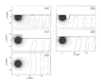
図5の(a)、(b)、(c)、(d)、(e)に、コアと空気層までの距離dairを0.0μmとした場合(半埋め込み導波路)、従来の代表的な屈曲損低減手法であるトレンチを有する構造の場合、本発明の実施形態において上クラッドの高さhを6.0μmとした場合、非特許文献6で提案した光導波路でコアと空気層までの距離dairを3.0μmとした場合(埋め込み導波路)、非特許文献6で取り上げた光導波路でコアと空気層までの距離dairを∞とした場合(完全埋め込み導波路)における固有モード界分布をそれぞれ比較して示す。図5(b)では、コアとトレンチとの間隔を3.0μmとし、トレンチ部の屈折率を1.0(空気)としている。これらの図では、位相の変化を明確にするために、界の実部Re{Hx}を表示している。
In the case of (a), (b), (c), (d), and (e) of FIG. 5, when the distance d air between the core and the air layer is 0.0 μm (semi-embedded waveguide), it is a conventional representative. In the case of a structure having a trench, which is a method for reducing bending loss, when the height h of the upper clad is 6.0 μm in the embodiment of the present invention, the optical waveguide proposed in
図5(a)のコアと空気層までの距離dair=0.0μmの半埋め込み導波路では、コアに局在する界の重心が-y方向にシフトし、顕著な漏れ波が観察される。図5(b)のトレンチを有する構造の光導波路では、漏れ波が抑圧されているが界の重心の-y方向へのシフトは改善されていない。図5(d)の埋め込み導波路では、漏れ波が抑圧されているが、コア中心(y=0)軸に対する界の非対称性が残っている。図5(e)の完全埋め込み導波路では、界はコア中心軸に関して対称になっているが、漏れ波が+y領域にも生じている。これに対し、本発明の実施形態において上クラッドの高さhを6.0μmとした導波路では、コアのほぼ中心に界のピークが現れ、同時に漏れ波が抑制されていることがわかる。また、この構造では、界の折り返し効果によって最も効率良く漏れ波を打ち消すため、半埋め込み導波路や埋め込み導波路や完全埋め込み導波路よりも純粋屈曲損を低減することができることがわかる。 In the semi-embedded waveguide with a distance d air = 0.0 μm between the core and the air layer in FIG. 5 (a), the center of gravity of the field localized in the core shifts in the −y direction, and a remarkable leak wave is observed. .. In the optical waveguide having the structure having the trench shown in FIG. 5B, the leakage wave is suppressed, but the shift of the center of gravity of the field in the −y direction is not improved. In the embedded waveguide of FIG. 5 (d), the leakage wave is suppressed, but the asymmetry of the field with respect to the core center (y = 0) axis remains. In the fully embedded waveguide of FIG. 5 (e), the fields are symmetrical with respect to the core central axis, but leakage waves also occur in the + y region. On the other hand, in the waveguide in which the height h of the upper clad is 6.0 μm in the embodiment of the present invention, it can be seen that the peak of the field appears at almost the center of the core and the leakage wave is suppressed at the same time. Further, it can be seen that in this structure, since the leakage wave is most efficiently canceled by the folding effect of the field, the pure bending loss can be reduced as compared with the semi-embedded waveguide, the embedded waveguide, and the fully embedded waveguide.
図6の(a)と(b)に、純粋屈曲損と偏波依存損(PDL)の波長特性をそれぞれ示す。これらの図には、比較として、埋め込み導波路とトレンチを有する導波路の結果を併記している。図6(a)より、本実施形態の光導波路では、波長1.3μmから1.65μmの広帯域に渡って、埋め込み導波路やトレンチを有する導波路よりも純粋屈曲損が低減されることがわかる。また、本実施形態の光導波路では、上クラッドを積層することによって、界の対称性が改善された状態で界がコアに集中するため、偏波依存損(PDL)も低減されることがわかる。更に、図6(b)より、本実施形態の光導波路では、偏波依存損(PDL)が0.007dB/cm以下に抑圧されることがわかる。 (A) and (b) of FIG. 6 show the wavelength characteristics of pure bending loss and polarization-dependent loss (PDL), respectively. For comparison, these figures also show the results of an embedded waveguide and a waveguide with a trench. From FIG. 6A, it can be seen that the optical waveguide of the present embodiment has a reduced pure bending loss over a wide band with a wavelength of 1.3 μm to 1.65 μm as compared with an embedded waveguide or a waveguide having a trench. .. Further, in the optical waveguide of the present embodiment, it can be seen that the polarization dependence loss (PDL) is also reduced because the field is concentrated on the core in a state where the symmetry of the field is improved by laminating the upper clad. .. Further, from FIG. 6B, it can be seen that in the optical waveguide of the present embodiment, the polarization-dependent loss (PDL) is suppressed to 0.007 dB / cm or less.
次に、屈曲部を有する光導波路における屈曲半径の依存性を調べた結果(屈曲半径Rに対する純粋屈曲損)を図7に示す。図7から、トレンチを有する光導波路では純粋屈曲損の偏波間差が大きいのに対し、埋め込み構造の光導波路や本実施形態の光導波路では偏波間差が殆どないことがわかる。 Next, the result of investigating the dependence of the bending radius in the optical waveguide having a bending portion (pure bending loss with respect to the bending radius R) is shown in FIG. From FIG. 7, it can be seen that the optical waveguide having a trench has a large difference between the polarizations of the pure bending loss, whereas the optical waveguide having an embedded structure and the optical waveguide of the present embodiment have almost no difference between the polarizations.
また、本実施形態の導波路では、その他の手法による導波路に比べ、屈曲半径R=6.0mmからR=8.0mmの屈曲半径で大きな損失低減効果が得られる利点がある。 Further, the waveguide of the present embodiment has an advantage that a large loss reduction effect can be obtained with a bending radius of R = 6.0 mm to R = 8.0 mm as compared with the waveguide by other methods.
次に、本発明による実施形態2~4に係る光導波路について図8~図10を参照して述べる。図8~図10において、図2と同様な要素には同じ番号を付して説明を省略する。 Next, the optical waveguide according to the second to fourth embodiments according to the present invention will be described with reference to FIGS. 8 to 10. In FIGS. 8 to 10, the same elements as those in FIG. 2 are designated by the same number, and the description thereof will be omitted.
図8は、本発明による実施形態2の光導波路20における屈曲部の断面を示す図である。この光導波路20では、コア21が、コア21の表面21Aが上クラッド23の内部となり、下面21Bが下クラッド22の内部となるように上クラッド23及び下クラッド22に埋め込まれる。図11(a)に、コア21Aの表面を下クラッド22の表面に対し2μm上側にシフトした場合の図5と同様の図を示す。h=6.0μmである。図11(a)から、図5(c)の場合に比べ、漏れ波がさらに抑圧され、損失低減効果が顕著であることがわかる。
FIG. 8 is a diagram showing a cross section of a bent portion in the
図9は、本発明による実施形態3の光導波路20における屈曲部の断面を示す図である。この光導波路20では、コア21が、コア21の表面21Aが上クラッド23の内部となり、かつ下面21Bが下クラッド22の表面22Aと同一表面となるように上クラッド23に埋め込まれる。図11(b)に、コア21Aの表面を下クラッド22の表面に対し6μm上側にシフトした場合の図5と同様の図を示す。h=6.0μmである。図11(b)から、図5(c)、図11(a)の場合に比べ、漏れ波がさらに抑圧され、損失低減効果が顕著であることがわかる。
FIG. 9 is a diagram showing a cross section of a bent portion in the
図10は、本発明による実施形態4の光導波路20における屈曲部の断面を示す図である。この光導波路20では、コア21が、コア21の表面21Aが上クラッド23の内部となり、かつ下面21Bも上クラッド23の内部となるように上クラッド23に埋め込まれる。図11(c)に、コア21Aの表面21Aを下クラッド22の表面に対し8μm上側にシフトした場合の図5と同様の図を示す。h=6.0μmである。図11(c)から、図5(c)、図11(a)、(b)の場合に比べ、漏れ波がさらに抑圧され、損失低減効果が顕著であることがわかる。
FIG. 10 is a diagram showing a cross section of a bent portion in the
図12に、コア21Aの表面21Aを下クラッド22の表面に対し上側にシフトさせた値をyshiftとした場合の純粋屈曲損を調べた結果を示す。R=7.0mm、λ=1.55μm、h=6.0μm、TMモードとした。図4に示すようにyshiftが0の状態でも損失低減効果は顕著であるが、yshiftが増えるに従い漏れ波がより抑圧され、損失低減効果がさらに顕著になることがわかる。
FIG. 12 shows the results of investigating the pure bending loss when the value obtained by shifting the
次に、本発明による実施形態5に係る光導波路について述べる。本実施形態では、各パラメータの表記は実施形態1~4と同様とする。 Next, the optical waveguide according to the fifth embodiment of the present invention will be described. In the present embodiment, the notation of each parameter is the same as that of the first to fourth embodiments.
本実施形態の光導波路のコアはシリコンで構成されている。各パラメータの数値例を示すと、コア幅wが0.32μm×0.32μm、nco=3.476、ncl=1.444、屈曲部の半径Rが2.0μmである。 The core of the optical waveguide of this embodiment is made of silicon. As a numerical example of each parameter, the core width w is 0.32 μm × 0.32 μm, n co = 3.476, n cl = 1.444, and the radius R of the bent portion is 2.0 μm.
図13の(a)と(b)に、本実施形態の光導波路において断面構造を図2とした場合、距離sLと距離sRが純粋屈曲損へ及ぼす影響を調べた結果を示す。図13の(a)に距離sLと距離sRに対するTEモードにおける純粋屈曲損の等高線を示し、図13の(b)に距離sLと距離sRに対するTMモードにおける純粋屈曲損の等高線を示す。ここでは、hを∞に固定し、使用動作波長λは1.55μmとした。図3の結果を得るために用いた石英系光導波路では、コアとクラッドの屈折率差が小さかったため、両モードの結果が同一となったが、シリコン光導波路では、コアとクラッドの屈折率差が大きいため、偏波で特性が異なる。なお、同程度に低損失となる位置は存在する。図13より、sL≧0.22μmに選ぶことで、十分に界の広がり効果を抑制できることがわかる。また、sL=sR=0.22μmに選ぶことで最小の純粋屈曲損を得ることができる。シリコン光導波路も、一般に、sLとsRは、それぞれ0.3w~1.5w、より好ましくは0.5w~wである。 13 (a) and 13 (b) show the results of investigating the effects of distance s L and distance s R on pure bending loss when the cross-sectional structure of the optical waveguide of this embodiment is shown in FIG. FIG. 13 (a) shows contour lines of pure bending loss in TE mode for distance s L and distance s R , and FIG. 13 (b) shows contour lines of pure bending loss in TM mode for distance s L and distance s R. show. Here, h is fixed at ∞, and the operating wavelength λ used is 1.55 μm. In the quartz-based optical waveguide used to obtain the result shown in FIG. 3, the difference in refractive index between the core and the clad was small, so that the results in both modes were the same. Because of the large size, the characteristics differ depending on the polarization. It should be noted that there are positions where the loss is as low as that. From FIG. 13, it can be seen that the effect of expanding the field can be sufficiently suppressed by selecting s L ≧ 0.22 μm. Further, the minimum pure bending loss can be obtained by selecting s L = s R = 0.22 μm. In the silicon optical waveguide, s L and s R are generally 0.3 w to 1.5 w, more preferably 0.5 w to w, respectively.
図14の(a)と(b)に、純粋屈曲損と偏波依存損(PDL)の波長特性をそれぞれ示す。ここでは、sL=sR=0.22μm、h=0.2μmとした。これらの図には、比較として、トレンチを有する光導波路の結果を併記している。図13(a)より、本実施形態の光導波路では、広帯域の波長に渡って、トレンチを有する光導波路よりも純粋屈曲損が低減されることがわかる。また、本実施形態の光導波路では、上クラッドを積層することによって、界の対称性が改善された状態で界がコアに集中するため、偏波依存損(PDL)も低減されることがわかる。更に、図14(b)より、本実施形態の光導波路では、偏波依存損が0.01dB/cm以下に抑圧されることがわかる。なお、シリコン光導波路において断面構造を図8,9,10としても石英系光導波路と同様に屈曲損低減効果を得ることができる。 14 (a) and 14 (b) show the wavelength characteristics of pure bending loss and polarization-dependent loss (PDL), respectively. Here, s L = s R = 0.22 μm and h = 0.2 μm. For comparison, these figures also show the results of an optical waveguide with a trench. From FIG. 13 (a), it can be seen that the optical waveguide of the present embodiment has a lower pure bending loss than the optical waveguide having a trench over a wide band wavelength. Further, in the optical waveguide of the present embodiment, it can be seen that the polarization dependence loss (PDL) is also reduced because the field is concentrated on the core in a state where the symmetry of the field is improved by laminating the upper clad. .. Further, from FIG. 14B, it can be seen that in the optical waveguide of the present embodiment, the polarization-dependent loss is suppressed to 0.01 dB / cm or less. Even if the cross-sectional structure of the silicon optical waveguide is shown in FIGS. 8, 9 and 10, the bending loss reducing effect can be obtained as in the quartz optical waveguide.
20 誘電体光導波路
21 コア
21A コアの表面
21B コアの下面
22 下クラッド
22A 下クラッドの表面
22AL、22AR 下クラッドの一部表面
23 上クラッド
24 空気層
20
Claims (6)
誘電体光導波路の横断面において、前記コアの横幅をwとしたとき、前記コアの右端と空気層までの距離sRと、前記コアの左端から空気層までの距離sLがそれぞれ0.3w~1.5wであるとともに、前記上クラッドの高さhがw以上であり、
前記コアが石英系材料から構成されており、屈曲部の屈曲半径が6~8mmであることを特徴とする屈曲部を有する誘電体光導波路。 A mesa-shaped upper clad is provided on the lower clad, and the core is located between a position where the surface of the core is flush with the surface of the lower clad and a position inside the upper clad. And / or at least the upper clad and the lower clad surface not covered by the upper clad, which are embedded in the upper clad, are in contact with the air layer.
In the cross section of the dielectric optical waveguide, when the width of the core is w, the distance sR between the right end of the core and the air layer and the distance sL from the left end of the core to the air layer are 0.3w to 1, respectively. .5w and the height h of the upper clad is w or more .
A dielectric optical waveguide having a bent portion, wherein the core is made of a quartz-based material and the bent portion has a bending radius of 6 to 8 mm .
誘電体光導波路の横断面において、前記コアの横幅をwとしたとき、前記コアの右端と空気層までの距離sRと、前記コアの左端から空気層までの距離sLがそれぞれ0.3w~1.5wであるとともに、前記上クラッドの高さhがw以上であり、 In the cross section of the dielectric optical waveguide, when the width of the core is w, the distance sR between the right end of the core and the air layer and the distance sL from the left end of the core to the air layer are 0.3w to 1, respectively. .5w and the height h of the upper clad is w or more.
前記コアがシリコンから構成されており、屈曲部の屈曲半径が2μmであることを特徴とする屈曲部を有する誘電体光導波路。A dielectric optical waveguide having a bent portion, wherein the core is made of silicon and the bent portion has a bending radius of 2 μm.
Applications Claiming Priority (2)
| Application Number | Priority Date | Filing Date | Title |
|---|---|---|---|
| JP2016138245 | 2016-07-13 | ||
| JP2016138245 | 2016-07-13 |
Publications (2)
| Publication Number | Publication Date |
|---|---|
| JP2018018059A JP2018018059A (en) | 2018-02-01 |
| JP7002092B2 true JP7002092B2 (en) | 2022-02-04 |
Family
ID=61081817
Family Applications (1)
| Application Number | Title | Priority Date | Filing Date |
|---|---|---|---|
| JP2017094009A Active JP7002092B2 (en) | 2016-07-13 | 2017-05-10 | Dielectric optical waveguide with bends |
Country Status (1)
| Country | Link |
|---|---|
| JP (1) | JP7002092B2 (en) |
Citations (3)
| Publication number | Priority date | Publication date | Assignee | Title |
|---|---|---|---|---|
| US20040076394A1 (en) | 2000-10-27 | 2004-04-22 | Federico Carniel | Hybrid buried/ridge planar waveguides |
| JP2006323136A (en) | 2005-05-19 | 2006-11-30 | Nippon Telegr & Teleph Corp <Ntt> | Optical waveguide and manufacturing method therefor |
| WO2016093187A1 (en) | 2014-12-10 | 2016-06-16 | 日本碍子株式会社 | External resonator type light-emitting device |
Family Cites Families (3)
| Publication number | Priority date | Publication date | Assignee | Title |
|---|---|---|---|---|
| JPH06263452A (en) * | 1993-03-05 | 1994-09-20 | Sumitomo Electric Ind Ltd | Production of optical waveguide |
| JPH11352344A (en) * | 1998-06-09 | 1999-12-24 | Nippon Telegr & Teleph Corp <Ntt> | Low crosstalk optical wiring |
| WO2000072060A1 (en) * | 1999-05-21 | 2000-11-30 | British Telecommunications Public Limited Company | Making grooves in planar silica optical waveguides |
-
2017
- 2017-05-10 JP JP2017094009A patent/JP7002092B2/en active Active
Patent Citations (3)
| Publication number | Priority date | Publication date | Assignee | Title |
|---|---|---|---|---|
| US20040076394A1 (en) | 2000-10-27 | 2004-04-22 | Federico Carniel | Hybrid buried/ridge planar waveguides |
| JP2006323136A (en) | 2005-05-19 | 2006-11-30 | Nippon Telegr & Teleph Corp <Ntt> | Optical waveguide and manufacturing method therefor |
| WO2016093187A1 (en) | 2014-12-10 | 2016-06-16 | 日本碍子株式会社 | External resonator type light-emitting device |
Non-Patent Citations (1)
| Title |
|---|
| NITO, Yuta, et al,A waveguide configuration for reducing both pure bend and polarization dependent losses,2016 URSI Asia-Pacific Radio Science Conference (URSI AP-RASC),米国,IEEE,2016年08月21日,pp.1393-1394 |
Also Published As
| Publication number | Publication date |
|---|---|
| JP2018018059A (en) | 2018-02-01 |
Similar Documents
| Publication | Publication Date | Title |
|---|---|---|
| JP5728140B1 (en) | High-order polarization conversion element, optical waveguide element, and DP-QPSK modulator | |
| JP6365855B2 (en) | Apparatus and method for a waveguide polarizer with a series of bends | |
| US10838146B2 (en) | Single mode waveguide with an adiabatic bend | |
| JP5588794B2 (en) | Substrate type optical waveguide device having grating structure, chromatic dispersion compensation element, and method of manufacturing substrate type optical waveguide device | |
| JP6069439B1 (en) | Polarization identification element | |
| JP2015532470A (en) | Curved optical waveguide | |
| JP2005128419A (en) | Optical waveguide structure and its manufacturing method | |
| WO2014030578A1 (en) | Optical waveguide element | |
| JP6798313B2 (en) | Rib-type optical waveguide and optical waveguide using it | |
| JP2006323210A (en) | Spot size converter | |
| JP7002092B2 (en) | Dielectric optical waveguide with bends | |
| JP6728997B2 (en) | Optical waveguide and optical integrated circuit | |
| JP2005301301A (en) | Optical coupler | |
| Lee et al. | Apexes-linked circle gratings for low-loss waveguide bends | |
| JP2012255987A (en) | Polarization-selective multimode interference waveguide device | |
| JP2017191253A (en) | Optical integrated circuit and manufacturing method thereof | |
| JP2015145991A (en) | Optical waveguide and method for manufacturing optical waveguide | |
| JP2006508383A (en) | Optical demultiplexing components with low polarization sensitivity and large processing tolerance | |
| JP5086164B2 (en) | Optical wavelength multiplexing / demultiplexing circuit | |
| US11662522B2 (en) | Optical waveguide device operated as mode converter | |
| WO2023243045A1 (en) | Directional coupler and manufacturing method therefor | |
| US11644612B2 (en) | Waveguide, manufacturing method of said waveguide and polarisation splitter which makes use of said waveguide | |
| Galarza et al. | Simple low-loss waveguide bends using ARROW effect | |
| JP5644630B2 (en) | Optical waveguide device | |
| JP6991259B2 (en) | Optical waveguide element |
Legal Events
| Date | Code | Title | Description |
|---|---|---|---|
| AA64 | Notification of invalidation of claim of internal priority (with term) |
Free format text: JAPANESE INTERMEDIATE CODE: A241764 Effective date: 20170620 |
|
| A521 | Request for written amendment filed |
Free format text: JAPANESE INTERMEDIATE CODE: A523 Effective date: 20170627 |
|
| A621 | Written request for application examination |
Free format text: JAPANESE INTERMEDIATE CODE: A621 Effective date: 20200422 |
|
| A131 | Notification of reasons for refusal |
Free format text: JAPANESE INTERMEDIATE CODE: A131 Effective date: 20210511 |
|
| A521 | Request for written amendment filed |
Free format text: JAPANESE INTERMEDIATE CODE: A523 Effective date: 20210623 |
|
| A131 | Notification of reasons for refusal |
Free format text: JAPANESE INTERMEDIATE CODE: A131 Effective date: 20210907 |
|
| RD02 | Notification of acceptance of power of attorney |
Free format text: JAPANESE INTERMEDIATE CODE: A7422 Effective date: 20210909 |
|
| A521 | Request for written amendment filed |
Free format text: JAPANESE INTERMEDIATE CODE: A523 Effective date: 20211029 |
|
| TRDD | Decision of grant or rejection written | ||
| A01 | Written decision to grant a patent or to grant a registration (utility model) |
Free format text: JAPANESE INTERMEDIATE CODE: A01 Effective date: 20211207 |
|
| A61 | First payment of annual fees (during grant procedure) |
Free format text: JAPANESE INTERMEDIATE CODE: A61 Effective date: 20211217 |
|
| R150 | Certificate of patent or registration of utility model |
Ref document number: 7002092 Country of ref document: JP Free format text: JAPANESE INTERMEDIATE CODE: R150 |