JP6997105B2 - Electronic switch and dimmer - Google Patents
Electronic switch and dimmer Download PDFInfo
- Publication number
- JP6997105B2 JP6997105B2 JP2018558747A JP2018558747A JP6997105B2 JP 6997105 B2 JP6997105 B2 JP 6997105B2 JP 2018558747 A JP2018558747 A JP 2018558747A JP 2018558747 A JP2018558747 A JP 2018558747A JP 6997105 B2 JP6997105 B2 JP 6997105B2
- Authority
- JP
- Japan
- Prior art keywords
- terminal
- power
- control
- electronic switch
- bidirectional electronic
- Prior art date
- Legal status (The legal status is an assumption and is not a legal conclusion. Google has not performed a legal analysis and makes no representation as to the accuracy of the status listed.)
- Active
Links
Images


Classifications
-
- H—ELECTRICITY
- H03—ELECTRONIC CIRCUITRY
- H03K—PULSE TECHNIQUE
- H03K17/00—Electronic switching or gating, i.e. not by contact-making and –breaking
- H03K17/51—Electronic switching or gating, i.e. not by contact-making and –breaking characterised by the components used
- H03K17/78—Electronic switching or gating, i.e. not by contact-making and –breaking characterised by the components used using opto-electronic devices, i.e. light-emitting and photoelectric devices electrically- or optically-coupled
- H03K17/785—Electronic switching or gating, i.e. not by contact-making and –breaking characterised by the components used using opto-electronic devices, i.e. light-emitting and photoelectric devices electrically- or optically-coupled controlling field-effect transistor switches
-
- G—PHYSICS
- G05—CONTROLLING; REGULATING
- G05F—SYSTEMS FOR REGULATING ELECTRIC OR MAGNETIC VARIABLES
- G05F1/00—Automatic systems in which deviations of an electric quantity from one or more predetermined values are detected at the output of the system and fed back to a device within the system to restore the detected quantity to its predetermined value or values, i.e. retroactive systems
- G05F1/10—Regulating voltage or current
- G05F1/12—Regulating voltage or current wherein the variable actually regulated by the final control device is ac
- G05F1/40—Regulating voltage or current wherein the variable actually regulated by the final control device is ac using discharge tubes or semiconductor devices as final control devices
- G05F1/44—Regulating voltage or current wherein the variable actually regulated by the final control device is ac using discharge tubes or semiconductor devices as final control devices semiconductor devices only
- G05F1/45—Regulating voltage or current wherein the variable actually regulated by the final control device is ac using discharge tubes or semiconductor devices as final control devices semiconductor devices only being controlled rectifiers in series with the load
-
- H—ELECTRICITY
- H02—GENERATION; CONVERSION OR DISTRIBUTION OF ELECTRIC POWER
- H02M—APPARATUS FOR CONVERSION BETWEEN AC AND AC, BETWEEN AC AND DC, OR BETWEEN DC AND DC, AND FOR USE WITH MAINS OR SIMILAR POWER SUPPLY SYSTEMS; CONVERSION OF DC OR AC INPUT POWER INTO SURGE OUTPUT POWER; CONTROL OR REGULATION THEREOF
- H02M5/00—Conversion of ac power input into ac power output, e.g. for change of voltage, for change of frequency, for change of number of phases
- H02M5/02—Conversion of ac power input into ac power output, e.g. for change of voltage, for change of frequency, for change of number of phases without intermediate conversion into dc
- H02M5/04—Conversion of ac power input into ac power output, e.g. for change of voltage, for change of frequency, for change of number of phases without intermediate conversion into dc by static converters
- H02M5/22—Conversion of ac power input into ac power output, e.g. for change of voltage, for change of frequency, for change of number of phases without intermediate conversion into dc by static converters using discharge tubes with control electrode or semiconductor devices with control electrode
- H02M5/275—Conversion of ac power input into ac power output, e.g. for change of voltage, for change of frequency, for change of number of phases without intermediate conversion into dc by static converters using discharge tubes with control electrode or semiconductor devices with control electrode using devices of a triode or transistor type requiring continuous application of a control signal
- H02M5/293—Conversion of ac power input into ac power output, e.g. for change of voltage, for change of frequency, for change of number of phases without intermediate conversion into dc by static converters using discharge tubes with control electrode or semiconductor devices with control electrode using devices of a triode or transistor type requiring continuous application of a control signal using semiconductor devices only
-
- H—ELECTRICITY
- H05—ELECTRIC TECHNIQUES NOT OTHERWISE PROVIDED FOR
- H05B—ELECTRIC HEATING; ELECTRIC LIGHT SOURCES NOT OTHERWISE PROVIDED FOR; CIRCUIT ARRANGEMENTS FOR ELECTRIC LIGHT SOURCES, IN GENERAL
- H05B45/00—Circuit arrangements for operating light-emitting diodes [LED]
- H05B45/10—Controlling the intensity of the light
-
- H—ELECTRICITY
- H05—ELECTRIC TECHNIQUES NOT OTHERWISE PROVIDED FOR
- H05B—ELECTRIC HEATING; ELECTRIC LIGHT SOURCES NOT OTHERWISE PROVIDED FOR; CIRCUIT ARRANGEMENTS FOR ELECTRIC LIGHT SOURCES, IN GENERAL
- H05B45/00—Circuit arrangements for operating light-emitting diodes [LED]
- H05B45/30—Driver circuits
- H05B45/37—Converter circuits
- H05B45/3725—Switched mode power supply [SMPS]
-
- H—ELECTRICITY
- H02—GENERATION; CONVERSION OR DISTRIBUTION OF ELECTRIC POWER
- H02J—CIRCUIT ARRANGEMENTS OR SYSTEMS FOR SUPPLYING OR DISTRIBUTING ELECTRIC POWER; SYSTEMS FOR STORING ELECTRIC ENERGY
- H02J50/00—Circuit arrangements or systems for wireless supply or distribution of electric power
- H02J50/10—Circuit arrangements or systems for wireless supply or distribution of electric power using inductive coupling
-
- H—ELECTRICITY
- H03—ELECTRONIC CIRCUITRY
- H03K—PULSE TECHNIQUE
- H03K2217/00—Indexing scheme related to electronic switching or gating, i.e. not by contact-making or -breaking covered by H03K17/00
- H03K2217/0009—AC switches, i.e. delivering AC power to a load
-
- Y—GENERAL TAGGING OF NEW TECHNOLOGICAL DEVELOPMENTS; GENERAL TAGGING OF CROSS-SECTIONAL TECHNOLOGIES SPANNING OVER SEVERAL SECTIONS OF THE IPC; TECHNICAL SUBJECTS COVERED BY FORMER USPC CROSS-REFERENCE ART COLLECTIONS [XRACs] AND DIGESTS
- Y02—TECHNOLOGIES OR APPLICATIONS FOR MITIGATION OR ADAPTATION AGAINST CLIMATE CHANGE
- Y02B—CLIMATE CHANGE MITIGATION TECHNOLOGIES RELATED TO BUILDINGS, e.g. HOUSING, HOUSE APPLIANCES OR RELATED END-USER APPLICATIONS
- Y02B20/00—Energy efficient lighting technologies, e.g. halogen lamps or gas discharge lamps
- Y02B20/30—Semiconductor lamps, e.g. solid state lamps [SSL] light emitting diodes [LED] or organic LED [OLED]
Description
関連出願の相互参照
本出願は、2016年5月12日に出願された「AC直接LVO電子調光スイッチ」と題する米国仮特許出願第62/335495号及び2016年12月9日に出願された「電子スイッチ及び調光器」と題する米国仮特許出願第62/431926号の優先権を主張する。両出願は、発明者が共通であり、現在継続中である。
Mutual reference to related applications This application was filed on May 12, 2016, US Provisional Patent Application No. 62/335495 and December 9, 2016, entitled "AC Direct LVO Electronic Dimmer". Claims the priority of US Provisional Patent Application No. 62/431926 entitled "Electronic Switches and Dimmers". Both applications have a common inventor and are currently ongoing.
連邦政府資金による研究開発の記載
未適用。
Federally funded R & D description not applicable.
技術分野
本発明は、電力管理システム、並びに電子スイッチ及び調光制御を提供する方法に関する。
Technical Fields The present invention relates to power management systems, as well as methods of providing electronic switches and dimming control.
関連する背景技術
家庭環境及びビジネス環境における交流(AC)電力への従来のアクセスは、設備電気システムに配線される機械的なコンセントにより供給される。これらのコンセントは、ヒューズや回路遮断器などの電気機械装置を用いて、過大な電気負荷又は潜在的に危険な地絡から保護される。同様に、照明や天井扇風機などの従来の部屋用電気機器の制御は、電気機械スイッチを用いて行われる。これらの基本的に機械的な制御装置は、単純なオン-オフ制御を提供し、必然的に摩耗し、経時的に短絡又は潜在的に危険なアーク放電を引き起こす可能性がある。
Related Background Technology Traditional access to alternating current (AC) power in home and business environments is provided by mechanical outlets wired to the equipment electrical system. These outlets are protected from excessive electrical loads or potentially dangerous ground faults using electromechanical devices such as fuses and circuit breakers. Similarly, control of conventional room electrical equipment such as lighting and ceiling fans is performed using electromechanical switches. These essentially mechanical controls provide simple on-off control, which can inevitably wear out and cause short circuits or potentially dangerous arc discharges over time.
一般的な電気機器のより微妙な制御は、典型的に、サイクル毎に交流電源波形を中断すること(いわゆる位相制御)を可能にするトライアックなどの電子デバイスにより提供される。これらに先行する可変抵抗器又は単巻変圧器よりはるかに効率的であるにも関わらず、トライアックは、小さなエンクロージャにおいて大きな電気的負荷の制御のために効果的に使用するには、依然としてかなり非効率的であり、設備電気システムへ電気ノイズを戻す可能性がある。 More subtle control of common electrical equipment is typically provided by electronic devices such as triacs that allow the AC power waveform to be interrupted (so-called phase control) on a cycle-by-cycle basis. Despite being much more efficient than the variable resistors or autotransformers that precede them, the triac is still quite non-useful for effective use in controlling large electrical loads in small enclosures. It is efficient and has the potential to return electrical noise to the equipment electrical system.
従って、設備電気システムにおける幅広い適用のための、より信頼性の高い高効率な制御オプションのより広い範囲を提供する改善された電子制御システムが必要とされる。さらに、低コストで製造できる高度な電力制御機能のための他の回路と統合できる半導体装置を用いて実現可能なそのような制御システムが必要とされる。 Therefore, there is a need for improved electronic control systems that provide a wider range of more reliable and efficient control options for a wide range of applications in equipment electrical systems. In addition, there is a need for such control systems that can be realized using semiconductor devices that can be integrated with other circuits for advanced power control functions that can be manufactured at low cost.
本発明は、単純なコンセントのオン-オフスイッチングから、例えば電灯の調光において印加される交流電力の連続的な変動にまで及ぶ設備電気システム全体の交流電力の制御に対する新しいアプローチに関する。 The present invention relates to a new approach to the control of AC power throughout the equipment electrical system, ranging from simple outlet on-off switching to continuous fluctuations in the AC power applied, for example in the dimming of lamps.
より具体的には、本発明は、一実施形態において交流電源波形のオン-オフ及び位相制御の両方を提供する機能の組み合わせに関する。 More specifically, the present invention relates to a combination of functions that provide both on-off and phase control of an AC power supply waveform in one embodiment.
一実施形態は、交流主電源及び所望の負荷の間に接続された非常に低い「オン」抵抗を有する電子スイッチとして、パワーMOS電界効果トランジスタ(MOSFETs)を使用する。典型的なパワーMOSFETsは、本来、ボディダイオードを導電チャネルと並列に結合するので、複数対のデバイスは、ソース端子を共通で備える背中合わせの配置で接続され、真に双方向的な(AC)スイッチ構成を提供する。パワーMOSFETsのスイッチング動作を制御するために、ドレインに接続され、ゲート-ソース間バイアス電圧をプリチャージし、それにより両デバイスを「オン」にする整流ダイオードと、隔離された光源により照明された際にゲート端子を共通ソース端子に短絡させて両デバイスを「オフ」状態にする光結合フォトトランジスタと、を用いた新規のフローティング制御回路が採用される。従って、パワーMOSFETスイッチは、光制御信号により強制的に「オフ」にされない限り、通常は「オン」である。光制御信号は、負荷に供給される電力の公称オン-オフ制御のために連続的に印加することができる。あるいは、光制御信号は、交流電源波形と同期して位相制御を提供することができる。光制御信号用の集積制御回路は、無効負荷のスイッチングに適した立ち上がりエッジ位相制御か、LEDなどの非線形負荷に適した立ち下がりエッジ位相制御のいずれかを提供することができる。 One embodiment uses power MOS field effect transistors (MOSFETs) as electronic switches with very low "on" resistance connected between an AC mains and a desired load. Since typical power MOSFETs inherently couple body diodes in parallel with conductive channels, multiple pairs of devices are connected in a back-to-back arrangement with a common source terminal and are truly bidirectional (AC) switches. Provide the configuration. When illuminated by an isolated light source and a rectifying diode connected to the drain to precharge the gate-source bias voltage to "on" both devices to control the switching operation of the power MOSFETs. A new floating control circuit using an optical coupling phototransistor that short-circuits the gate terminal to the common source terminal and puts both devices in the "off" state is adopted. Therefore, the power MOSFET switch is normally "on" unless it is forcibly turned "off" by an optical control signal. Optical control signals can be applied continuously for nominal on-off control of the power delivered to the load. Alternatively, the optical control signal can provide phase control in synchronization with the AC power supply waveform. An integrated control circuit for an optical control signal can provide either rising edge phase control suitable for ineffective load switching or falling edge phase control suitable for non-linear loads such as LEDs.
特定の実施例は、本発明の概念を例示的な応用に限定することを意図するものではない。本発明の他の態様及び利点は、添付の図面及び詳細な説明から明らかにされる。 The specific examples are not intended to limit the concepts of the invention to exemplary applications. Other aspects and advantages of the invention will be apparent from the accompanying drawings and detailed description.
図1は、交流電源101から負荷108に供給される電力を制御する基本的なパワーMOSFET双方向スイッチを示す概略図である。パワーMOSFETs102及び103は、それぞれボディダイオード104及び105を備える。スイッチ106は、パワーMOSFETs102及び103に印加されるゲート-ソース間バイアス電圧を制御する。「オン」位置において、バイアス電圧107は、パワーMOSFETsのゲート端子に印加される。電圧107は、反転層を形成させ、それにより各デバイスのドレインからソースへ延びる導電チャネルを生成するパワーMOSFETsの閾値電圧(典型的には5~10ボルト)より大きい電圧である。この「オン」状態において、各パワーMOSFETのドレイン-ソース挙動は、低値の抵抗Rdsとしてモデル化できる。ドレイン及びソース間の電圧降下が約0.6ボルト未満に維持される限り、ボディダイオードは、非導電性に維持され、無視することができる。「オン」状態において、図1の回路は、等価的に、2Rdsの値を持つ直列抵抗器を介して交流電源101に接続される負荷108である。
FIG. 1 is a schematic diagram showing a basic power MOSFET bidirectional switch that controls the power supplied from the
スイッチ106の「オフ」位置において、パワーMOSFETsのゲート端子はソース端子に短絡され、ドレイン-ソース間導電チャネルは、ドレイン-ソース間電圧がボディダイオードの降伏電圧未満を維持する限り、消滅する。「オフ」状態において、図1の回路は、等価的に、背中合わせのボディダイオード104及び105を介して交流電源101に接続される負荷108であり、負荷108を電源101から効果的に切断する。
In the "off" position of the
「オフ」状態において、パワーMOSFETsのドレイン-ソース間電圧がボディダイオードの降伏電圧Vbr未満を維持するという要件は、ボディダイオードの降伏電圧が交流電源101のピーク電圧を超えることを要求する。従って、例えば、電源101が共通の120ボルト(rms)の交流電源に対応すると仮定すると、各ボディダイオードの降伏電圧は、170ボルトのピーク電源電圧を超えなければならない。
The requirement that the drain-source voltage of the power MOSFETs be kept below the breakdown voltage Vbr of the body diode in the "off" state requires that the breakdown voltage of the body diode exceeds the peak voltage of the
パワーMOSFET構造のより詳細な分析は、ボディダイオードが、事実上、MOSFETチャネルと並列に接続されたバイポーラトランジスタのベース-コレクタ接合であることを示す。付加的な寄生素子は、ベース-コレクタ接合のキャパシタンス、並びにベース及びエミッタ間の寄生抵抗を有する。この交流結合回路は、ドレイン-ソース間電圧の変化率dVds/dtに制約を課してベース-エミッタ接合が順方向にバイアスすることを防止し、これによりMOSFETチャネルが「オフ」の間にバイポーラトランジスタを導通させる。結果として生じる漏れ電流は、負荷108にエネルギーを与えるのに十分でないかもしれないが、付加的な効率又は安全性への懸念を引き起こすのに十分大きい可能性がある。
A more detailed analysis of the power MOSFET structure shows that the body diode is effectively a base-collector junction of bipolar transistors connected in parallel with the MOSFET channel. The additional parasitic element has a base-collector junction capacitance as well as a parasitic resistance between the base and the emitter. This AC coupling circuit imposes a constraint on the rate of change dV ds / dt of the drain-source voltage to prevent the base-emitter junction from being biased forward, thereby during the MOSFET channel "off". Conduct the bipolar transistor. The resulting leakage current may not be sufficient to energize the
同様に、「オン」状態における制約を考慮するには、Rds*Iloadで与えられる各パワーMOSFETのドレイン-ソース間電圧降下が約0.6ボルト未満であることを必要とする。潜在的により重要なことは、Rds*Iload2で与えられ、「オン」状態の各パワーMOSFETにおいて消散される電力が、過度の温度上昇を避けるために数ワット未満を維持しなければならないということである。従って、例えば、一般家庭用回路を20アンペアの典型的な制限を有する120ボルトの交流電源から切り替えるには、各パワーMOSFETのRdsが0.005オーム(5ミリオーム)未満であることを必要とする。 Similarly, to take into account the constraints in the "on" state, the drain-source voltage drop of each power MOSFET given by R ds * Iload needs to be less than about 0.6 volts. Potentially more importantly, the power given by R ds * Iload 2 and dissipated in each "on" power MOSFET must be maintained at less than a few watts to avoid excessive temperature rise. That is. So, for example, switching a general household circuit from a 120 volt AC power supply with a typical limit of 20 amps requires that the R ds of each power MOSFET be less than 0.005 ohms (5 milliohms). do.
デバイスの構造及びドーピングレベルを変化させることにより、ボディダイオードの降伏電圧をRdsの値に対してトレードオフできることは、当該技術分野において周知である。具体的には、Rdsの値はVbr 2.5に比例することが示されている。従って、例えば、Vbrを半分にカットすると、Rdsが5.7分の1に減少する。 It is well known in the art that the breakdown voltage of the body diode can be traded off for the value of R ds by varying the structure and doping level of the device. Specifically, it has been shown that the value of R ds is proportional to V br 2.5 . Therefore, for example, if V br is cut in half, R ds is reduced to 1/5.7.
図1の回路は、スイッチ106及び電圧源107を備える概念的なバイアススイッチング回路が、ソース101のピークからピークの範囲全体に亘って変化する背中合わせのパワーMOSFETs102及び103の共通ソース端子に対し、電気的に浮遊することを示している。概念は単純にもかかわらず、該回路は、実際には低コストで実現することが難しい可能性がある。
In the circuit of FIG. 1, a conceptual bias switching circuit comprising a
図2は、制御回路に対する従来技術のアプローチを示す概略図である。図1の電圧源106は、光起電力ダイオードスタック201により置き換えられている。光起電力ダイオードスタック201は、別個の低電圧源203により電力が供給され、電流制限抵抗器205を介してスイッチ204により制御される発光ダイオード(LED)206により照明される場合に、必要なゲート-ソース間バイアス電圧を供給する。素子203~206は、ダイオードスタック201の光学的近傍の範囲内にあると想定される。LED206がスイッチオフされた場合、ダイオードスタック201の両端の電圧は、抵抗器202を介してドレインされ、パワーMOSFETsが「オフ」状態となる。
FIG. 2 is a schematic diagram showing a prior art approach to a control circuit. The
図2の回路が単純なオン-オフスイッチングアプリケーション用に動作するにもかかわらず、バイアス回路を介したパワーMOSFETsのゲート-ソース間キャパシタンスの充電及び放電に関連する時定数は、典型的に、50/60Hzの交流電源で位相制御を行うには大きすぎてしまう。 Despite the fact that the circuit of FIG. 2 works for simple on-off switching applications, the time constant associated with charging and discharging the gate-source capacitance of power MOSFETs via a bias circuit is typically 50. It is too large for phase control with a / 60Hz AC power supply.
図3は、改良されたスイッチ回路の基本的要素を示す概略図である。パワーMOSFETsは、以下の説明において論じられる好適な実施形態のスイッチングデバイスであるが、改良された回路において、他の形式の電界効果トランジスタを有利に採用することができることは、当業者にとって明らかであろう。図1のように、電圧107は、パワーMOSFETs102及び103を「オン」状態にバイアスするために用いられる。図1の回路における動作とは反対に、スイッチ106が開いたままである限り、パワーMOSFETsは「オン」のみとなる。スイッチ106が閉じた場合、ゲート及びソースが共に短絡され、電圧107が抵抗器300を通過して降下するので、パワーMOSFETsは強制的に「オフ」状態となる。
FIG. 3 is a schematic diagram showing the basic elements of an improved switch circuit. Although power MOSFETs are switching devices of preferred embodiments discussed in the following description, it will be apparent to those skilled in the art that other types of field effect transistors can be advantageously employed in improved circuits. Let's do it. As shown in FIG. 1, the
図4は、本発明の回路の一実施形態を示す概略図である。図1の電圧源106は、スイッチングユニット400において、パワーMOSFETsの閾値電圧より大きいツェナー電圧を有するツェナーダイオード402に置き換えられている。ツェナーダイオード402は、それぞれパワーMOSFETsのドレイン端子に接続され、電流制限抵抗器403及び405により保護される整流ダイオード404及び406を介してバイアスされる。従って、照射がない場合には、抵抗器-ダイオード分岐部403-404及び405-406は、ドレイン端子のいずれもがツェナー電圧を超えたとき、ツェナーダイオード402にバイアスを与え、パワーMOSFETs102及び103を「オン」状態にする。LED206により照明されると、フォトトランジスタ401は、分岐部403-404及び405-406からパワーMOSFETsのソース端子へバイアス電流をシャントして、パワーMOSFETsを「オフ」状態にする。本回路において、ターンオン時定数は、電流制限抵抗器403及び405の値及びパワーMOSFETsのゲート-ソース間のキャパシタンスにより決定される。一方、ターンオフ時定数は、LED206により供給される照明レベルでのフォトトランジスタ401の飽和電流によって決定される。これらの時定数は両方とも、交流電源の周期よりもはるかに短く設定することができ、これにより、本実施形態は、オン-オフ及び位相制御モードの両方で動作することができる。
FIG. 4 is a schematic diagram showing an embodiment of the circuit of the present invention. The
図5は、回路のパフォーマンス向上のために2つのスイッチユニット400を用いた図4の実施形態の概略図である。本実施形態において、パワーMOSFETsは、図4において用いられるユニットの半分の降伏電圧を有するように選択されると仮定する。従って、個々のスイッチユニットのオン抵抗は、上述のように、5.7分の1に減少すると予想され、直列に接続された2つのスイッチユニットの合計オン抵抗は、図4の回路に対して2.8分の1に減少する。さらに、「オフ」状態にある各スイッチユニット間の電圧降下は半分になり、これにより各ユニットが経験するdVds/dtを2分の1に減少させ、結果として「オフ」状態の漏れ電流が減少する。
FIG. 5 is a schematic diagram of an embodiment of FIG. 4 in which two
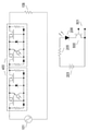
図5はまた、LED206の照明を制御する電子スイッチ回路を含む。LED206を通る電圧源203からの電流は、抵抗器205により制限され、トランジスタ500により制御される。トランジスタ500は、制御端子501に印加される外部の制御電圧により制御される。これにより、外部の制御回路(図示せず)を介して交流主波形と同期してLEDの迅速なスイッチングが可能となり、調光アプリケーションで使用されるものと同様に、印加される交流波形の位相制御を提供する。他の実施形態において、制御信号は、交流電源波形と同期し、調整可能なパルス幅を有する一連のパルスであり、負荷に供給される平均電流/電力を効果的に制御し、これにより、光源の負荷に対する調光効果及びACモータ負荷の速度制御を提供する。他の実施形態において、制御信号は、交流電源波形とは独立した固定周波数又は可変周波数を有する一連のパルスであり、これにより、無線充電器/発電機として使用するための負荷端子に無線周波数(RF)電力波形を生成する。他の実施形態において、制御信号は、LEDの可変照明を可能とする可変直流電圧であり、これによりMOSFETsを線形モードで動作させることができる。
FIG. 5 also includes an electronic switch circuit that controls the illumination of the
図6は、図5と同様の一実施形態の概略図であるが、交流電源の各アームに個々のスイッチユニット400が配置されている。発明者は、この回路構成がスイッチデバイスのターンオフ特性をさらに改善し、漏れ電流をさらに減少させることを見出した。
FIG. 6 is a schematic view of an embodiment similar to FIG. 5, in which
図7は、交流電源の各アームに2つのスイッチユニット400を用いて、回路のパフォーマンスをさらに改善する図6の実施形態の概略図である。本実施形態においては、図3において用いられるユニットの4分の1の降伏電圧を有するパワーMOSFETsが選択されると仮定する。従って、個々のスイッチユニットのオン抵抗は、上述のように、32分の1に減少すると予想され、直列に接続された2つのスイッチユニットの合計オン抵抗は、図4の回路に対して8分の1に減少する。さらに、「オフ」状態にある各スイッチユニット間の電圧降下は4分の1になり、これにより各ユニットが経験するdVds/dtを4分の1に減少させ、結果として図4の回路に対し、「オフ」状態の漏れ電流がさらに減少する。上述のように、発明者は、この回路構成がスイッチデバイスのターンオフ特性をさらに改善し、漏れ電流をさらに減少させることを見出した。
FIG. 7 is a schematic diagram of an embodiment of FIG. 6 in which two
まとめ
設備電気システム全体にわたる交流電力の制御に対する新しいアプローチについて説明されている。本アプローチは、スイッチを「オン」状態に自己バイアスし、光結合制御素子を用いてスイッチを強制的に「オフ」状態にする、光学的に結合され、電気的に浮遊した制御回路を有する双方向スイッチサブ回路構成のパワーMOSFETsを使用する。制御回路の時定数は、オン-オフ制御及び位相制御を可能にするのに十分に速い。改善されたパフォーマンスを提供するために、複数のサブ回路を容易にカスケード接続することができる。
Summary Describes a new approach to AC power control throughout the equipment electrical system. This approach has both optically coupled, electrically floating control circuits that self-bias the switch to an "on" state and force the switch to an "off" state using an optical coupling control element. Power MOSFETs with a switch sub-circuit configuration are used. The time constant of the control circuit is fast enough to enable on-off control and phase control. Multiple subcircuits can be easily cascaded to provide improved performance.
Claims (19)
a.各スイッチデバイスがドレイン端子、ソース端子及びゲート端子を備え、前記ゲート端子及び前記ソース端子間に規定される閾値電圧により特徴付けられる第1及び第2の直列接続電子スイッチデバイスであって、前記第1のスイッチデバイスの前記ドレイン端子は、前記スイッチ回路の前記入力端子を備え、前記第2のスイッチデバイスのドレイン端子は、前記スイッチ回路の前記出力端子を備え、前記第1及び第2のスイッチデバイスの前記ソース端子は、第1のスイッチデバイス制御端子において相互接続され、前記第1及び第2のスイッチデバイスの前記ゲート端子は、第2のスイッチデバイス制御端子において相互接続される、第1及び第2の直列接続電子スイッチデバイスと、
b.前記スイッチデバイスの前記閾値電圧より大きい電圧を有し、電流制御抵抗器を介して前記第1及び第2のスイッチデバイス制御端子間に印加される電圧源であって、
a.前記スイッチ回路の前記入力端子から前記第2のスイッチデバイス制御端子に接続される第1の整流装置と、
b.前記スイッチ回路の前記出力端子から前記第2のスイッチデバイス制御端子に接続される第2の整流装置と、
c.前記第1のスイッチデバイス制御端子から前記第2のスイッチデバイス制御端子に接続される電圧調整装置と、を有する電圧源と、
c.前記第1及び第2のスイッチデバイス制御端子間に接続されるスイッチと、
をさらに備える双方向電子スイッチ回路。 A bidirectional electronic switch circuit with an input terminal and an output terminal.
a. A first and second series-connected electronic switch device, wherein each switch device comprises a drain terminal, a source terminal and a gate terminal and is characterized by a threshold voltage defined between the gate terminal and the source terminal. The drain terminal of the switch device 1 comprises the input terminal of the switch circuit, the drain terminal of the second switch device comprises the output terminal of the switch circuit, and the first and second switch devices. The source terminals of the first and second switch devices are interconnected at the first switch device control terminal, and the gate terminals of the first and second switch devices are interconnected at the second switch device control terminal, first and second. 2 series connection electronic switch devices and
b. A voltage source having a voltage higher than the threshold voltage of the switch device and being applied between the first and second switch device control terminals via a current control resistor.
a. A first rectifier connected from the input terminal of the switch circuit to the second switch device control terminal, and
b. A second rectifier connected from the output terminal of the switch circuit to the second switch device control terminal, and
c. A voltage source having a voltage regulator connected from the first switch device control terminal to the second switch device control terminal.
c. The switch connected between the first and second switch device control terminals and
Also equipped with a bidirectional electronic switch circuit.
a.入射する照明の強度に比例するコンダクタンスにより特徴付けられ、前記第1のスイッチデバイス制御端子から前記第2のスイッチデバイス制御端子に接続される光活性化電子デバイスと、
b.第1の制御端子及び第2の制御端子を有するトランジスタにより制御され、前記光活性化電子デバイスを照明するように構成された発光素子であって、前記発光素子により放出される光の強度が、前記第1の制御端子と前記第2の制御端子との間に印加される外部制御信号の振幅に比例する、発光素子と、を備える請求項1の双方向電子スイッチ回路。 The switch is
a. A light-activated electronic device characterized by conductance proportional to the intensity of incident illumination and connected from the first switch device control terminal to the second switch device control terminal.
b. A light emitting device controlled by a transistor having a first control terminal and a second control terminal and configured to illuminate the photoactivated electronic device, wherein the intensity of light emitted by the light emitting device is determined. The bidirectional electronic switch circuit according to claim 1, further comprising a light emitting element proportional to the amplitude of an external control signal applied between the first control terminal and the second control terminal.
前記エミッタ端子は、前記スイッチデバイスの前記共通ソース端子に接続され、前記コレクタ端子は、前記スイッチデバイスの前記共通ゲート端子に接続される請求項2の双方向電子スイッチ回路。 The photoactivated electronic device comprises a semiconductor phototransistor having a collector terminal and an emitter terminal.
The bidirectional electronic switch circuit according to claim 2, wherein the emitter terminal is connected to the common source terminal of the switch device, and the collector terminal is connected to the common gate terminal of the switch device.
a.交流電源から電力を受け取るための第1及び第2の電力入力端子と、
b.前記負荷装置に交流電力を供給するための第1及び第2の電力出力端子と、
c.前記双方向電子スイッチ回路の前記入力端子を前記第1の電力入力端子に接続し、前記双方向電子スイッチ回路の前記出力端子を前記第1の電力出力端子に接続することと、
d.前記第2の電力入力端子を前記第2の電力出力端子に接続することと、
e.前記トランジスタの前記第1及び第2の制御端子に電子制御信号を供給することと、
を含む方法。 The method of using the bidirectional electronic switch circuit according to claim 2 for connecting AC power to a load device.
a. The first and second power input terminals for receiving power from the AC power supply,
b. The first and second power output terminals for supplying AC power to the load device, and
c. By connecting the input terminal of the bidirectional electronic switch circuit to the first power input terminal and connecting the output terminal of the bidirectional electronic switch circuit to the first power output terminal.
d. By connecting the second power input terminal to the second power output terminal,
e. Supplying electronic control signals to the first and second control terminals of the transistor,
How to include.
a.交流電源から電力を受け取るための第1及び第2の電力入力端子と、
b.前記負荷装置に交流電力を供給するための第1及び第2の電力出力端子と、
c.第1及び第2の双方向電子スイッチ回路と、
d.前記第1の双方向電子スイッチ回路の前記入力端子を前記第1の電力入力端子に接続し、前記第1の双方向電子スイッチ回路の前記出力端子を前記第1の電力出力端子に接続することと、
e.前記第2の双方向電子スイッチ回路の前記入力端子を前記第2の電力入力端子に接続し、前記第2の双方向電子スイッチ回路の前記出力端子を前記第2の電力出力端子に接続することと、
f.前記トランジスタの前記第1及び第2の制御端子に電子制御信号を供給することと、
を含む方法。 The method of using the bidirectional electronic switch circuit according to claim 2 for connecting AC power to a load device.
a. The first and second power input terminals for receiving power from the AC power supply,
b. The first and second power output terminals for supplying AC power to the load device, and
c. The first and second bidirectional electronic switch circuits,
d. The input terminal of the first bidirectional electronic switch circuit is connected to the first power input terminal, and the output terminal of the first bidirectional electronic switch circuit is connected to the first power output terminal. When,
e. The input terminal of the second bidirectional electronic switch circuit is connected to the second power input terminal, and the output terminal of the second bidirectional electronic switch circuit is connected to the second power output terminal. When,
f. Supplying electronic control signals to the first and second control terminals of the transistor,
How to include.
a.交流電源から電力を受け取るための第1及び第2の電力入力端子と、
b.前記負荷装置に交流電力を供給するための第1及び第2の電力出力端子と、
c.直列構成に配列された複数の双方向電子スイッチ回路を備える回路アレイであって、最初の双方向電子スイッチ回路の前記入力端子は、前記回路アレイの前記入力端子であり、
最後の前記双方向電子スイッチ回路の前記出力端子が前記回路アレイの前記出力端子であること、全ての前記双方向電子スイッチ回路の前記第1の制御端子が相互接続され、前記回路アレイの前記第1の制御端子を形成すること、及び、全ての前記双方向電子スイッチ回路の前記第2の制御端子が相互接続され、前記回路アレイの前記第2の制御端子を形成することを除いては、各後続の双方向電子スイッチ回路の前記入力端子が前の前記双方向電子スイッチ回路の前記出力端子に接続される、前記回路アレイと、
d.前記回路アレイの前記入力端子を前記第1の電力入力端子に接続し、前記回路アレイの前記出力端子を前記第1の電力出力端子に接続することと、
e.前記第2の電力入力端子を前記第2の電力出力端子に接続することと、
f.前記トランジスタの前記第1及び第2の制御端子に電子制御信号を供給することと、
を含む方法。 The method of using the bidirectional electronic switch circuit according to claim 2 for connecting AC power to a load device.
a. The first and second power input terminals for receiving power from the AC power supply,
b. The first and second power output terminals for supplying AC power to the load device, and
c. A circuit array comprising a plurality of bidirectional electronic switch circuits arranged in series, wherein the input terminal of the first bidirectional electronic switch circuit is the input terminal of the circuit array.
The output terminal of the last bidirectional electronic switch circuit is the output terminal of the circuit array, the first control terminal of all the bidirectional electronic switch circuits is interconnected, and the first control terminal of the circuit array is connected. Except for forming one control terminal and interconnecting the second control terminals of all the bidirectional electronic switch circuits to form the second control terminal of the circuit array. With the circuit array, the input terminal of each subsequent bidirectional electronic switch circuit is connected to the output terminal of the previous bidirectional electronic switch circuit.
d. By connecting the input terminal of the circuit array to the first power input terminal and connecting the output terminal of the circuit array to the first power output terminal.
e. By connecting the second power input terminal to the second power output terminal,
f. Supplying electronic control signals to the first and second control terminals of the transistor,
How to include.
a.交流電源から電力を受け取るための第1及び第2の電力入力端子と、
b.前記負荷装置に交流電力を供給するための第1及び第2の電力出力端子と、
c.直列構成に配列された複数の双方向電子スイッチ回路をそれぞれ備える第1及び第2の回路アレイであって、最初の双方向電子スイッチ回路の前記入力端子は、前記第1及び第2の回路アレイの前記入力端子であり、
最後の前記双方向電子スイッチ回路の前記出力端子が前記第1及び第2の回路アレイの前記出力端子であること、全ての前記双方向電子スイッチ回路の前記第1の制御端子が相互接続され、前記第1及び第2の回路アレイの前記第1の制御端子を形成すること、及び、全ての前記双方向電子スイッチ回路の前記第2の制御端子が相互接続され、前記第1及び第2の回路アレイの前記第2の制御端子を形成することを除いては、各後続の双方向電子スイッチ回路の前記入力端子が前の前記双方向電子スイッチ回路の前記出力端子に接続される、前記第1及び第2の回路アレイと、
d.前記第1の回路アレイの前記入力端子を前記第1の電力入力端子に接続し、前記第1の回路アレイの前記出力端子を前記第1の電力出力端子に接続することと、
e.前記第2の回路アレイの前記入力端子を前記第2の電力入力端子に接続し、前記回路アレイの前記出力端子を前記第2の電力出力端子に接続することと、
f.前記トランジスタの前記第1及び第2の制御端子に電子制御信号を供給することと、
を含む方法。 The method of using the bidirectional electronic switch circuit according to claim 2 for connecting AC power to a load device.
a. The first and second power input terminals for receiving power from the AC power supply,
b. The first and second power output terminals for supplying AC power to the load device, and
c. A first and second circuit array including a plurality of bidirectional electronic switch circuits arranged in series, respectively, wherein the input terminal of the first bidirectional electronic switch circuit is the first and second circuit arrays. It is the input terminal of
The output terminal of the last bidirectional electronic switch circuit is the output terminal of the first and second circuit arrays, and the first control terminal of all the bidirectional electronic switch circuits is interconnected. The first and second control terminals of the first and second circuit arrays are formed, and the second control terminals of all the bidirectional electronic switch circuits are interconnected. The second control terminal of each subsequent bidirectional electronic switch circuit is connected to the output terminal of the previous bidirectional electronic switch circuit, except that it forms the second control terminal of the circuit array. With the first and second circuit arrays,
d. By connecting the input terminal of the first circuit array to the first power input terminal and connecting the output terminal of the first circuit array to the first power output terminal.
e. By connecting the input terminal of the second circuit array to the second power input terminal and connecting the output terminal of the circuit array to the second power output terminal.
f. Supplying electronic control signals to the first and second control terminals of the transistor,
How to include.
それぞれアノード端子及びカソード端子を有する第1及び第2の半導体ダイオードを備え、
前記第1の半導体ダイオードの前記アノード端子は、電流制御抵抗器を介して前記双方向スイッチ回路の前記入力端子に接続され、前記第2の半導体ダイオードの前記アノード端子は、電流制御抵抗器を介して前記双方向電子スイッチ回路の前記出力端子に接続され、前記第1及び第2の半導体ダイオードの前記カソード端子は、前記第2のスイッチデバイス制御端子に接続される請求項1の双方向電子スイッチ回路。 The first and second rectifiers are
It comprises first and second semiconductor diodes having an anode terminal and a cathode terminal, respectively.
The anode terminal of the first semiconductor diode is connected to the input terminal of the bidirectional switch circuit via a current control resistor, and the anode terminal of the second semiconductor diode is connected to the input terminal of the bidirectional switch circuit via a current control resistor. The bidirectional electronic switch according to claim 1, wherein the cathode terminal of the first and second semiconductor diodes is connected to the output terminal of the bidirectional electronic switch circuit, and the cathode terminal of the first and second semiconductor diodes is connected to the second switch device control terminal. circuit.
Applications Claiming Priority (5)
| Application Number | Priority Date | Filing Date | Title |
|---|---|---|---|
| US201662335495P | 2016-05-12 | 2016-05-12 | |
| US62/335,495 | 2016-05-12 | ||
| US201662431926P | 2016-12-09 | 2016-12-09 | |
| US62/431,926 | 2016-12-09 | ||
| PCT/US2017/030415 WO2017196572A1 (en) | 2016-05-12 | 2017-05-01 | Electronic switch and dimmer |
Publications (3)
| Publication Number | Publication Date |
|---|---|
| JP2019515468A JP2019515468A (en) | 2019-06-06 |
| JP2019515468A5 JP2019515468A5 (en) | 2020-06-18 |
| JP6997105B2 true JP6997105B2 (en) | 2022-01-17 |
Family
ID=60266790
Family Applications (1)
| Application Number | Title | Priority Date | Filing Date |
|---|---|---|---|
| JP2018558747A Active JP6997105B2 (en) | 2016-05-12 | 2017-05-01 | Electronic switch and dimmer |
Country Status (5)
| Country | Link |
|---|---|
| US (2) | US10469077B2 (en) |
| EP (1) | EP3455938B1 (en) |
| JP (1) | JP6997105B2 (en) |
| CN (1) | CN109314511B (en) |
| WO (1) | WO2017196572A1 (en) |
Cited By (2)
| Publication number | Priority date | Publication date | Assignee | Title |
|---|---|---|---|---|
| US11764565B2 (en) | 2018-07-07 | 2023-09-19 | Intelesol, Llc | Solid-state power interrupters |
| US11791616B2 (en) | 2018-10-01 | 2023-10-17 | Intelesol, Llc | Solid-state circuit interrupters |
Families Citing this family (19)
| Publication number | Priority date | Publication date | Assignee | Title |
|---|---|---|---|---|
| EP3455938B1 (en) * | 2016-05-12 | 2023-06-28 | Intelesol, LLC | Electronic switch and dimmer |
| KR102399201B1 (en) * | 2016-10-28 | 2022-05-17 | 인테레솔, 엘엘씨 | Controls and Methods of AC Power Sources to Identify Loads |
| US10819336B2 (en) | 2017-12-28 | 2020-10-27 | Intelesol, Llc | Electronic switch and dimmer |
| US11056981B2 (en) | 2018-07-07 | 2021-07-06 | Intelesol, Llc | Method and apparatus for signal extraction with sample and hold and release |
| US11671029B2 (en) | 2018-07-07 | 2023-06-06 | Intelesol, Llc | AC to DC converters |
| US10993082B2 (en) | 2018-09-27 | 2021-04-27 | Amber Solutions, Inc. | Methods and apparatus for device location services |
| US11205011B2 (en) | 2018-09-27 | 2021-12-21 | Amber Solutions, Inc. | Privacy and the management of permissions |
| US11197153B2 (en) | 2018-09-27 | 2021-12-07 | Amber Solutions, Inc. | Privacy control and enhancements for distributed networks |
| US10936749B2 (en) | 2018-09-27 | 2021-03-02 | Amber Solutions, Inc. | Privacy enhancement using derived data disclosure |
| US11334388B2 (en) | 2018-09-27 | 2022-05-17 | Amber Solutions, Inc. | Infrastructure support to enhance resource-constrained device capabilities |
| US10985548B2 (en) | 2018-10-01 | 2021-04-20 | Intelesol, Llc | Circuit interrupter with optical connection |
| US11336096B2 (en) | 2018-11-13 | 2022-05-17 | Amber Solutions, Inc. | Managing power for residential and commercial networks |
| CN113455105A (en) | 2018-12-17 | 2021-09-28 | 因特莱索有限责任公司 | AC driven light emitting diode system |
| US11348752B2 (en) | 2019-05-18 | 2022-05-31 | Amber Solutions, Inc. | Intelligent circuit breakers with air-gap and solid-state switches |
| US11664741B2 (en) * | 2019-07-25 | 2023-05-30 | Susan Rhodes | System and method for AC power control |
| US11721508B2 (en) | 2019-12-06 | 2023-08-08 | Amber Semiconductor, Inc. | Solid-state ground-fault circuit interrupter |
| EP4088125A4 (en) | 2020-01-21 | 2024-03-06 | Amber Semiconductor Inc | Intelligent circuit interruption |
| CN115668735A (en) * | 2020-08-05 | 2023-01-31 | 安博半导体公司 | Two-wire electronic switch and dimmer |
| EP4197086A1 (en) | 2020-08-11 | 2023-06-21 | Amber Semiconductor, Inc. | Intelligent energy source monitoring and selection control system |
Family Cites Families (52)
| Publication number | Priority date | Publication date | Assignee | Title |
|---|---|---|---|---|
| US4074345A (en) | 1976-11-02 | 1978-02-14 | Ackermann Walter J | Electronic power supply |
| US4127895A (en) | 1977-08-19 | 1978-11-28 | Krueger Paul J | Charge-transfer voltage converter |
| US4500802A (en) * | 1982-06-21 | 1985-02-19 | Eaton Corporation | Three terminal bidirectional source to source FET circuit |
| US4487458A (en) * | 1982-09-28 | 1984-12-11 | Eaton Corporation | Bidirectional source to source stacked FET gating circuit |
| DE3240778A1 (en) | 1982-11-04 | 1984-05-10 | Siemens AG, 1000 Berlin und 8000 München | ELECTRONIC SWITCH |
| US4649302A (en) | 1984-07-30 | 1987-03-10 | Eaton Corporation | DC or AC solid state switch with improved line-derived control circuit power supply |
| US4682061A (en) | 1986-05-01 | 1987-07-21 | Honeywell Inc. | MOSFET transistor switch control |
| US4888504A (en) * | 1988-10-07 | 1989-12-19 | International Rectifier Corporation | Bidirectional MOSFET switching circuit with single gate bias |
| US5006737A (en) | 1989-04-24 | 1991-04-09 | Motorola Inc. | Transformerless semiconductor AC switch having internal biasing means |
| US5510747A (en) * | 1993-11-30 | 1996-04-23 | Siliconix Incorporated | Gate drive technique for a bidirectional blocking lateral MOSFET |
| US5654880A (en) | 1996-01-16 | 1997-08-05 | California Institute Of Technology | Single-stage AC-to-DC full-bridge converter with magnetic amplifiers for input current shaping independent of output voltage regulation |
| JP3756616B2 (en) * | 1996-02-22 | 2006-03-15 | 利康 鈴木 | Switching circuit, 3-terminal switching circuit, switching circuit, 3-terminal switching circuit, switching circuit, 3-terminal switching circuit, switching circuit, 3-terminal switching circuit and switching circuit |
| DE19631477A1 (en) | 1996-08-03 | 1998-02-05 | Bosch Gmbh Robert | Adjustable voltage divider arrangement manufactured in hybrid technology |
| US6169391B1 (en) | 1999-07-12 | 2001-01-02 | Supertex, Inc. | Device for converting high voltage alternating current to low voltage direct current |
| TWM244584U (en) * | 2000-01-17 | 2004-09-21 | Semiconductor Energy Lab | Display system and electrical appliance |
| US6420905B1 (en) * | 2000-09-07 | 2002-07-16 | John Haven Davis | Vented CMOS dynamic logic system |
| US6538906B1 (en) | 2002-02-11 | 2003-03-25 | Delta Electronics, Inc. | Energy storage circuit for DC-DC converter |
| JP4110380B2 (en) * | 2002-09-05 | 2008-07-02 | 富士ゼロックス株式会社 | Display recording medium and information writing apparatus |
| US20050162139A1 (en) * | 2004-01-23 | 2005-07-28 | Mark Hirst | Alternating current switching circuit |
| US7297603B2 (en) * | 2005-03-31 | 2007-11-20 | Semiconductor Components Industries, L.L.C. | Bi-directional transistor and method therefor |
| US7654401B2 (en) | 2005-05-16 | 2010-02-02 | Donald Obergoenner | Wood joint for a barrelhead |
| US7164589B1 (en) * | 2005-07-11 | 2007-01-16 | International Rectifier Corporation | Bridgeless bi-directional forward type converter |
| AU2006324378B2 (en) * | 2005-12-12 | 2013-05-02 | Clipsal Australia Pty Ltd | Current zero crossing detector in a dimmer circuit |
| US7746677B2 (en) | 2006-03-09 | 2010-06-29 | Avago Technologies Wireless Ip (Singapore) Pte. Ltd. | AC-DC converter circuit and power supply |
| US7619365B2 (en) * | 2006-04-10 | 2009-11-17 | Lutron Electronics Co., Inc. | Load control device having a variable drive circuit |
| US7595680B2 (en) * | 2007-01-25 | 2009-09-29 | Panasonic Corporation | Bidirectional switch and method for driving the same |
| US7633239B2 (en) * | 2007-03-12 | 2009-12-15 | Masco Corporation | Dimming circuit for controlling electrical power |
| US7729147B1 (en) | 2007-09-13 | 2010-06-01 | Henry Wong | Integrated circuit device using substrate-on-insulator for driving a load and method for fabricating the same |
| GB2457085B (en) * | 2008-02-02 | 2010-03-17 | Russell Jacques | Bipolar power control |
| US7948719B2 (en) * | 2008-10-15 | 2011-05-24 | Masco Corporation | Solid state circuit protection system that works with arc fault circuit interrupter |
| US8072158B2 (en) * | 2009-03-25 | 2011-12-06 | General Electric Company | Dimming interface for power line |
| US8922133B2 (en) * | 2009-04-24 | 2014-12-30 | Lutron Electronics Co., Inc. | Smart electronic switch for low-power loads |
| JP5501667B2 (en) * | 2009-06-17 | 2014-05-28 | パナソニック株式会社 | AC / DC switch |
| US8729729B2 (en) | 2009-06-18 | 2014-05-20 | Mikhail Fridberg | Method and apparatus for driving low-power loads from AC sources |
| KR101379157B1 (en) * | 2009-08-26 | 2014-03-28 | 파나소닉 주식회사 | Load control device |
| US8664881B2 (en) * | 2009-11-25 | 2014-03-04 | Lutron Electronics Co., Inc. | Two-wire dimmer switch for low-power loads |
| US8957662B2 (en) * | 2009-11-25 | 2015-02-17 | Lutron Electronics Co., Inc. | Load control device for high-efficiency loads |
| US20110292703A1 (en) | 2010-05-29 | 2011-12-01 | Cuks, Llc | Single-stage AC-to-DC converter with isolation and power factor correction |
| JP2012004253A (en) * | 2010-06-15 | 2012-01-05 | Panasonic Corp | Bidirectional switch, two-wire ac switch, switching power circuit, and method for driving bidirectional switch |
| JP5711040B2 (en) * | 2011-04-28 | 2015-04-30 | トランスフォーム・ジャパン株式会社 | Bidirectional switch and charge / discharge protection device using the same |
| US8941264B2 (en) * | 2011-06-20 | 2015-01-27 | Bae Systems Information And Electronic Systems Integration Inc. | Apparatus for bi-directional power switching in low voltage vehicle power distribution systems |
| US9287792B2 (en) | 2012-08-13 | 2016-03-15 | Flextronics Ap, Llc | Control method to reduce switching loss on MOSFET |
| US9391525B2 (en) | 2012-09-24 | 2016-07-12 | Dialog Semiconductor Inc. | Power system switch protection using output driver regulation |
| TWI554034B (en) * | 2012-10-15 | 2016-10-11 | 陳家德 | Infrared ray on/off switch with automatic dimming capacity |
| CN103853060B (en) * | 2012-11-30 | 2017-06-23 | 上海拜骋电器有限公司 | The controller and control method of electronic switch, electronic switch and electronic equipment |
| US9264034B2 (en) * | 2013-12-19 | 2016-02-16 | Nxp B.V. | Circuit and method for body biasing |
| US9621053B1 (en) | 2014-08-05 | 2017-04-11 | Flextronics Ap, Llc | Peak power control technique for primary side controller operation in continuous conduction mode |
| US9443845B1 (en) * | 2015-02-23 | 2016-09-13 | Freescale Semiconductor, Inc. | Transistor body control circuit and an integrated circuit |
| MX2018002609A (en) * | 2015-09-04 | 2018-06-20 | Lutron Electronics Co | Load control device for high-efficiency loads. |
| EP3455938B1 (en) * | 2016-05-12 | 2023-06-28 | Intelesol, LLC | Electronic switch and dimmer |
| EP3249815B1 (en) * | 2016-05-23 | 2019-08-28 | NXP USA, Inc. | Circuit arrangement for fast turn-off of bi-directional switching device |
| US10756662B2 (en) * | 2017-06-09 | 2020-08-25 | Lutron Technology Company Llc | Motor control device |
-
2017
- 2017-05-01 EP EP17796572.0A patent/EP3455938B1/en active Active
- 2017-05-01 WO PCT/US2017/030415 patent/WO2017196572A1/en unknown
- 2017-05-01 JP JP2018558747A patent/JP6997105B2/en active Active
- 2017-05-01 US US16/092,839 patent/US10469077B2/en active Active - Reinstated
- 2017-05-01 CN CN201780027382.9A patent/CN109314511B/en active Active
-
2019
- 2019-09-12 US US16/568,571 patent/US10812072B2/en active Active
Cited By (2)
| Publication number | Priority date | Publication date | Assignee | Title |
|---|---|---|---|---|
| US11764565B2 (en) | 2018-07-07 | 2023-09-19 | Intelesol, Llc | Solid-state power interrupters |
| US11791616B2 (en) | 2018-10-01 | 2023-10-17 | Intelesol, Llc | Solid-state circuit interrupters |
Also Published As
| Publication number | Publication date |
|---|---|
| EP3455938B1 (en) | 2023-06-28 |
| US20200007126A1 (en) | 2020-01-02 |
| JP2019515468A (en) | 2019-06-06 |
| CN109314511A (en) | 2019-02-05 |
| EP3455938A4 (en) | 2019-11-20 |
| CN109314511B (en) | 2023-10-20 |
| WO2017196572A1 (en) | 2017-11-16 |
| EP3455938A1 (en) | 2019-03-20 |
| US10812072B2 (en) | 2020-10-20 |
| US10469077B2 (en) | 2019-11-05 |
| US20190140640A1 (en) | 2019-05-09 |
Similar Documents
| Publication | Publication Date | Title |
|---|---|---|
| JP6997105B2 (en) | Electronic switch and dimmer | |
| JP7037656B2 (en) | Electronic switch and dimmer | |
| CN110249515B (en) | Electronic switch and dimmer | |
| US8283875B2 (en) | Holding current circuits for phase-cut power control | |
| KR101975333B1 (en) | Driving circuitry for led lighting with reduced total harmonic distortion | |
| US8686668B2 (en) | Current offset circuits for phase-cut power control | |
| TW201406197A (en) | Arrangement and method for driving light-emitting diodes | |
| US11239742B2 (en) | Load control device having an overcurrent protection circuit | |
| US20120043893A1 (en) | Dimmable LED Power Supply | |
| CN104735860A (en) | Bleeder circuit controller | |
| EP3079446A1 (en) | Dimming circuit |
Legal Events
| Date | Code | Title | Description |
|---|---|---|---|
| A521 | Request for written amendment filed |
Free format text: JAPANESE INTERMEDIATE CODE: A523 Effective date: 20190109 |
|
| RD01 | Notification of change of attorney |
Free format text: JAPANESE INTERMEDIATE CODE: A7426 Effective date: 20190708 |
|
| A521 | Request for written amendment filed |
Free format text: JAPANESE INTERMEDIATE CODE: A821 Effective date: 20190708 |
|
| A521 | Request for written amendment filed |
Free format text: JAPANESE INTERMEDIATE CODE: A523 Effective date: 20200430 |
|
| A621 | Written request for application examination |
Free format text: JAPANESE INTERMEDIATE CODE: A621 Effective date: 20200430 |
|
| A977 | Report on retrieval |
Free format text: JAPANESE INTERMEDIATE CODE: A971007 Effective date: 20200826 |
|
| A131 | Notification of reasons for refusal |
Free format text: JAPANESE INTERMEDIATE CODE: A131 Effective date: 20200908 |
|
| A521 | Request for written amendment filed |
Free format text: JAPANESE INTERMEDIATE CODE: A523 Effective date: 20201204 |
|
| A131 | Notification of reasons for refusal |
Free format text: JAPANESE INTERMEDIATE CODE: A131 Effective date: 20210302 |
|
| A02 | Decision of refusal |
Free format text: JAPANESE INTERMEDIATE CODE: A02 Effective date: 20210831 |
|
| A521 | Request for written amendment filed |
Free format text: JAPANESE INTERMEDIATE CODE: A523 Effective date: 20211021 |
|
| C60 | Trial request (containing other claim documents, opposition documents) |
Free format text: JAPANESE INTERMEDIATE CODE: C60 Effective date: 20211021 |
|
| A911 | Transfer to examiner for re-examination before appeal (zenchi) |
Free format text: JAPANESE INTERMEDIATE CODE: A911 Effective date: 20211028 |
|
| C21 | Notice of transfer of a case for reconsideration by examiners before appeal proceedings |
Free format text: JAPANESE INTERMEDIATE CODE: C21 Effective date: 20211102 |
|
| TRDD | Decision of grant or rejection written | ||
| A01 | Written decision to grant a patent or to grant a registration (utility model) |
Free format text: JAPANESE INTERMEDIATE CODE: A01 Effective date: 20211130 |
|
| A61 | First payment of annual fees (during grant procedure) |
Free format text: JAPANESE INTERMEDIATE CODE: A61 Effective date: 20211216 |
|
| R150 | Certificate of patent or registration of utility model |
Ref document number: 6997105 Country of ref document: JP Free format text: JAPANESE INTERMEDIATE CODE: R150 |