EP3455938B1 - Electronic switch and dimmer - Google Patents
Electronic switch and dimmer Download PDFInfo
- Publication number
- EP3455938B1 EP3455938B1 EP17796572.0A EP17796572A EP3455938B1 EP 3455938 B1 EP3455938 B1 EP 3455938B1 EP 17796572 A EP17796572 A EP 17796572A EP 3455938 B1 EP3455938 B1 EP 3455938B1
- Authority
- EP
- European Patent Office
- Prior art keywords
- terminal
- control
- electronic switch
- bidirectional
- switch circuit
- Prior art date
- Legal status (The legal status is an assumption and is not a legal conclusion. Google has not performed a legal analysis and makes no representation as to the accuracy of the status listed.)
- Active
Links
- 230000002457 bidirectional effect Effects 0.000 claims description 41
- 239000004065 semiconductor Substances 0.000 claims description 9
- 238000000034 method Methods 0.000 claims description 7
- 238000005286 illumination Methods 0.000 claims description 6
- 230000000694 effects Effects 0.000 claims description 3
- 230000001360 synchronised effect Effects 0.000 claims description 3
- 238000003491 array Methods 0.000 claims 2
- 238000010586 diagram Methods 0.000 description 14
- 230000015556 catabolic process Effects 0.000 description 7
- 230000003287 optical effect Effects 0.000 description 5
- 230000005669 field effect Effects 0.000 description 2
- 230000003071 parasitic effect Effects 0.000 description 2
- 239000007787 solid Substances 0.000 description 2
- 238000007599 discharging Methods 0.000 description 1
- 230000005693 optoelectronics Effects 0.000 description 1
Images


Classifications
-
- H—ELECTRICITY
- H03—ELECTRONIC CIRCUITRY
- H03K—PULSE TECHNIQUE
- H03K17/00—Electronic switching or gating, i.e. not by contact-making and –breaking
- H03K17/51—Electronic switching or gating, i.e. not by contact-making and –breaking characterised by the components used
- H03K17/78—Electronic switching or gating, i.e. not by contact-making and –breaking characterised by the components used using opto-electronic devices, i.e. light-emitting and photoelectric devices electrically- or optically-coupled
- H03K17/785—Electronic switching or gating, i.e. not by contact-making and –breaking characterised by the components used using opto-electronic devices, i.e. light-emitting and photoelectric devices electrically- or optically-coupled controlling field-effect transistor switches
-
- G—PHYSICS
- G05—CONTROLLING; REGULATING
- G05F—SYSTEMS FOR REGULATING ELECTRIC OR MAGNETIC VARIABLES
- G05F1/00—Automatic systems in which deviations of an electric quantity from one or more predetermined values are detected at the output of the system and fed back to a device within the system to restore the detected quantity to its predetermined value or values, i.e. retroactive systems
- G05F1/10—Regulating voltage or current
- G05F1/12—Regulating voltage or current wherein the variable actually regulated by the final control device is ac
- G05F1/40—Regulating voltage or current wherein the variable actually regulated by the final control device is ac using discharge tubes or semiconductor devices as final control devices
- G05F1/44—Regulating voltage or current wherein the variable actually regulated by the final control device is ac using discharge tubes or semiconductor devices as final control devices semiconductor devices only
- G05F1/45—Regulating voltage or current wherein the variable actually regulated by the final control device is ac using discharge tubes or semiconductor devices as final control devices semiconductor devices only being controlled rectifiers in series with the load
-
- H—ELECTRICITY
- H02—GENERATION; CONVERSION OR DISTRIBUTION OF ELECTRIC POWER
- H02M—APPARATUS FOR CONVERSION BETWEEN AC AND AC, BETWEEN AC AND DC, OR BETWEEN DC AND DC, AND FOR USE WITH MAINS OR SIMILAR POWER SUPPLY SYSTEMS; CONVERSION OF DC OR AC INPUT POWER INTO SURGE OUTPUT POWER; CONTROL OR REGULATION THEREOF
- H02M5/00—Conversion of ac power input into ac power output, e.g. for change of voltage, for change of frequency, for change of number of phases
- H02M5/02—Conversion of ac power input into ac power output, e.g. for change of voltage, for change of frequency, for change of number of phases without intermediate conversion into dc
- H02M5/04—Conversion of ac power input into ac power output, e.g. for change of voltage, for change of frequency, for change of number of phases without intermediate conversion into dc by static converters
- H02M5/22—Conversion of ac power input into ac power output, e.g. for change of voltage, for change of frequency, for change of number of phases without intermediate conversion into dc by static converters using discharge tubes with control electrode or semiconductor devices with control electrode
- H02M5/275—Conversion of ac power input into ac power output, e.g. for change of voltage, for change of frequency, for change of number of phases without intermediate conversion into dc by static converters using discharge tubes with control electrode or semiconductor devices with control electrode using devices of a triode or transistor type requiring continuous application of a control signal
- H02M5/293—Conversion of ac power input into ac power output, e.g. for change of voltage, for change of frequency, for change of number of phases without intermediate conversion into dc by static converters using discharge tubes with control electrode or semiconductor devices with control electrode using devices of a triode or transistor type requiring continuous application of a control signal using semiconductor devices only
-
- H—ELECTRICITY
- H05—ELECTRIC TECHNIQUES NOT OTHERWISE PROVIDED FOR
- H05B—ELECTRIC HEATING; ELECTRIC LIGHT SOURCES NOT OTHERWISE PROVIDED FOR; CIRCUIT ARRANGEMENTS FOR ELECTRIC LIGHT SOURCES, IN GENERAL
- H05B45/00—Circuit arrangements for operating light-emitting diodes [LED]
- H05B45/10—Controlling the intensity of the light
-
- H—ELECTRICITY
- H05—ELECTRIC TECHNIQUES NOT OTHERWISE PROVIDED FOR
- H05B—ELECTRIC HEATING; ELECTRIC LIGHT SOURCES NOT OTHERWISE PROVIDED FOR; CIRCUIT ARRANGEMENTS FOR ELECTRIC LIGHT SOURCES, IN GENERAL
- H05B45/00—Circuit arrangements for operating light-emitting diodes [LED]
- H05B45/30—Driver circuits
- H05B45/37—Converter circuits
- H05B45/3725—Switched mode power supply [SMPS]
-
- H—ELECTRICITY
- H02—GENERATION; CONVERSION OR DISTRIBUTION OF ELECTRIC POWER
- H02J—CIRCUIT ARRANGEMENTS OR SYSTEMS FOR SUPPLYING OR DISTRIBUTING ELECTRIC POWER; SYSTEMS FOR STORING ELECTRIC ENERGY
- H02J50/00—Circuit arrangements or systems for wireless supply or distribution of electric power
- H02J50/10—Circuit arrangements or systems for wireless supply or distribution of electric power using inductive coupling
-
- H—ELECTRICITY
- H03—ELECTRONIC CIRCUITRY
- H03K—PULSE TECHNIQUE
- H03K2217/00—Indexing scheme related to electronic switching or gating, i.e. not by contact-making or -breaking covered by H03K17/00
- H03K2217/0009—AC switches, i.e. delivering AC power to a load
-
- Y—GENERAL TAGGING OF NEW TECHNOLOGICAL DEVELOPMENTS; GENERAL TAGGING OF CROSS-SECTIONAL TECHNOLOGIES SPANNING OVER SEVERAL SECTIONS OF THE IPC; TECHNICAL SUBJECTS COVERED BY FORMER USPC CROSS-REFERENCE ART COLLECTIONS [XRACs] AND DIGESTS
- Y02—TECHNOLOGIES OR APPLICATIONS FOR MITIGATION OR ADAPTATION AGAINST CLIMATE CHANGE
- Y02B—CLIMATE CHANGE MITIGATION TECHNOLOGIES RELATED TO BUILDINGS, e.g. HOUSING, HOUSE APPLIANCES OR RELATED END-USER APPLICATIONS
- Y02B20/00—Energy efficient lighting technologies, e.g. halogen lamps or gas discharge lamps
- Y02B20/30—Semiconductor lamps, e.g. solid state lamps [SSL] light emitting diodes [LED] or organic LED [OLED]
Definitions
- the invention relates to a power management system and methods to provide an electronic switch and dimming control.
- triacs which allow the AC mains waveform to be interrupted on a cycle-by-cycle basis, so-called phase control.
- phase control is typically provided by electronic devices such as triacs which allow the AC mains waveform to be interrupted on a cycle-by-cycle basis, so-called phase control.
- triacs are still too inefficient to be used effectively in small enclosures for the control of large electrical loads and can induce electrical noise back into the facility electrical system.
- the present invention relates to a novel approach for the control of AC power throughout a facility electrical system ranging from simple outlet on-off switching to continuous variation of the applied AC power for, for example, the dimming of electrical lights. More particularly the invention relates to a combination of functions that provides in one embodiment both on-off and phase-control of the AC mains waveform.
- MOSFETs power MOS field-effect transistors
- AC AC
- a novel floating control circuit uses rectifying diodes connected at the drains to precharge the gate-source bias voltage thereby turning both devices "on”, and an optically coupled phototransistor that shorts the gate terminals to the common source terminal to force the devices into their "off' state when illuminated by an isolated optical source.
- the power MOSFET switches are normally "on” unless forced “off' by the optical control signal.
- the optical control signal can be applied continuously for nominal on-off control of the power delivered to the load, or it can be synchronized with the AC mains waveform to provide phase control.
- Integrated control circuitry for the optical control signal can provide either leading edge phase control preferred for switching reactive loads or trailing edge phase control preferred for nonlinear loads such as LEDs.
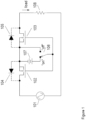
- FIG. 1 is a schematic diagram showing the basic power MOSFET bidirectional switch controlling the power delivered from AC source 101 to load 108.
- Power MOSFETs 102 and 103 include body diodes 104 and 105, respectively.
- Switch 106 controls the gate-to-source bias voltage applied to power MOSFETs 102 and 103.
- bias voltage 107 is applied to the gate terminals of the power MOSFETs.
- Voltage 107 is a voltage greater than the threshold voltage of the power MOSFETs (typically 5 to 10 volts) causing an inversion layer to form thereby creating a conducting channel extending from the drain to the source of each device.
- each power MOSFET In this "on" state, the drain-to-source behavior of each power MOSFET can be modeled as a low value resistor, R ds . As long as the voltage drop between drain and source remains below about 0.6 volt, the body diodes remain nonconductive and can be neglected.
- the circuit of Figure 1 is equivalently the load 108 connected to AC source 101 through a series resistor having value 2R ds .
- V br The requirement that the drain-to-source voltage of the power MOSFETs remain below the breakdown voltage of the body diodes, V br , in the "off" state requires that the breakdown voltage of the body diodes exceed the peak voltage of AC source 101.
- source 101 corresponds to a common 120 volt (rms) AC mains
- the breakdown voltage of each body diode must exceed the peak source voltage of 170 volts.
- a more detailed analysis of the power MOSFET structure shows that the body diode is effectively the base-collector junction of a bipolar transistor connected in parallel with the MOSFET channel. Additional parasitic elements include the capacitance of the base-collector junction and a parasitic resistance between the base and the emitter.
- This AC-coupled circuit places a constraint on the rate of change of the drain-to-source voltage, dV ds /dt, to avoid forward biasing the base-emitter junction, thereby causing the bipolar transistor to conduct while the MOSFET channel is "off'. While the resulting leakage current may not be sufficient to energize the load 108, it may be large enough to cause additional efficiency or safety concerns.
- the breakdown voltage of the body diode can be advantageously traded off against the value of R ds by varying the structure and the doping levels in the device.
- the value of R ds is proportional to V br 2.5 .
- cutting V br in half results in reducing R ds by a factor of 5.7.
- the circuit of Figure 1 shows that the conceptual bias switching circuit comprising switch 106 and voltage source 107 floats electrically with the common source terminals of the back-to-back power MOSFETs 102 and 103 which vary across the entire peak-to-peak range of source 101.
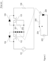
- FIG. 2 shows a schematic diagram of a prior art approach to the control circuit.
- Voltage source 106 in Figure 1 is replaced with a photovoltaic diode stack 201 that provides the needed gate-to-source bias voltage when illuminated by a light emitting diode (LED) 206 which is powered by a separate low voltage source 203 and controlled by switch 204 through current limiting resistor 205.
- LED light emitting diode
- Elements 203-206 are assumed to be within optical proximity of diode stack 201.
- LED 206 is switched off, the voltage across diode stack 201 is drained through resistor 202 and the power MOSFETs enter the "off' state.
- FIG 3 is a schematic diagram showing the basic elements of the improved switch circuit.
- power MOSFETs are the preferred embodiment switching devices discussed in the following description, it will be apparent to one skilled in the art that other types of field-effect transistors can be advantageously employed in the improved circuit.
- voltage 107 is used to bias power MOSFETs 102 and 103 into their "on” state.
- the power MOSFETs are "on” only as long as switch 106 remains open.
- switch 106 is closed the power MOSFETs are forced to enter their "off' state since their gates and sources are shorted together and voltage 107 is dropped across resistor 300.
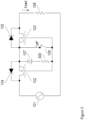
- FIG 4 is a schematic diagram showing an embodiment of the inventive circuit.
- Voltage source 106 in Figure 1 is replaced in switching unit 400 with a Zener diode 402 having a Zener voltage greater than the threshold voltage of the power MOSFETs.
- Zener diode 402 is biased through rectifier diodes 404 and 406 connected at the drain terminals of the power MOSFETs and protected by current limiting resistors 403 and 405, respectively.
- current limiting resistors 403-404 and 405-406 provide bias for Zener diode 402 when either of the drain terminals exceeds the Zener voltage, placing power MOSFETs 102 and 103 in the "on" state.
- phototransistor 401 When illuminated by LED 206 phototransistor 401 shunts the bias current from branches 403-404 and 405-406 to the source terminals of the power MOSFETS placing them in the "off" state.
- the turn-on time constant is dictated by the value of the current limiting resistors 403 and 405 and the gate-to-source capacitance of the power MOSFETs, while the turn-off time constant is dictated by the saturation current of the phototransistor 401 at the illumination level provided by LED 206. Both of these time constants can be designed to be much shorter than the period of the AC mains, thereby allowing this embodiment to operate in both an on-off and a phase-control mode.
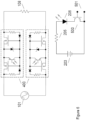
- Figure 5 is a schematic diagram of the embodiment of Figure 4 using two switch units 400 to improve the performance of the circuit.
- the power MOSFETs are selected to have half the breakdown voltage of the units used in Figure 4 .
- the on resistance of the individual switch units can be expected to be reduced by a factor of 5.7, as described above, and the total on resistance of the two switch units connected in series is reduced by a factor of 2.8 relative to the circuit in
- Figure 5 also includes an electronic switch circuit to control the illumination of LED 206.
- the current through LED 206 from voltage source 203 is limited by resistor 205 and is controlled by transistor 500.
- Transistor 500 is controlled by an external control voltage applied to control terminals 501. This allows for the rapid switching of the LED in synchronism with the AC mains waveform through external control circuitry (not shown) to provide phase control of the applied AC waveform, as is used in dimmer applications.
- control signal is a train of pulses synchronized with the AC mains waveform and having adjustable pulse widths to effectively control the average current/power delivered to the load, thereby providing a dimming effect for a light source load and a speed control for an AC motor load.
- control signal is a train of pulses having a fixed or variable frequency independent of the AC mains waveform thereby generating a radio-frequency (RF) power waveform at the load terminals for use as a wireless charger/generator.
- RF radio-frequency
- control signal is a variable DC voltage allowing variable illumination of the LED thereby allowing the MOSFETs to operate in a linear mode.
- Figure 6 is a schematic diagram of an embodiment similar to that of Figure 5 , but with an individual switch unit 400 placed in each arm of the AC power supply. The inventor has found that this circuit configuration further improves the turn-off characteristics of the switch devices, further reducing leakage currents.
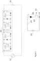
- Figure 7 is a schematic diagram of the embodiment of Figure 6 using two switch units 400 in each arm of the AC supply to further improve the performance of the circuit.
- the power MOSFETs are selected to have one-fourth the breakdown voltage of the units used in Figure 3 .
- the on resistance of the individual switch units can be expected to be reduced by a factor of 32, as described above, and the total on resistance of the two switch units connected in series is reduced by a factor of 8 relative to the circuit in Figure 4 .
- a novel approach for the control of AC power throughout a facility electrical system uses power MOSFETs in a bidirectional switch subcircuit configuration having an optically coupled, electrically floating control circuit that self-biases the switches into the "on” state and uses an optically coupled control element to force the switches into the "off' state.
- the time constant of the control circuit is fast enough to allow phase control as well as on-off control.
- a plurality of subcircuits can be easily cascaded to provide improved performance.
Description
- This application claims priority to
U.S. Provisional Application 62/335495. Titled: AC Direct LVO Electronic Dimming Switch, Filed May 12, 2016 U.S. Provisional Patent Application 62/431926 Titled: Electronic Switch and Dimmer filed December 9, 2016 - Not Applicable.
- The invention relates to a power management system and methods to provide an electronic switch and dimming control.
- Traditional access to alternating current (AC) electrical power in home and business environments is provided by mechanical outlets that are wired into the facility electrical system. These outlets are protected from excessive electrical loads or potentially dangerous ground faults using electromechanical devices such as fuses and circuit breakers. Similarly, the control of conventional electrical room appliances such as lighting and ceiling fans occurs using electromechanical switches. These fundamentally mechanical control devices provide simple on-off control and inevitably wear out and, over time, can cause short circuits or potentially dangerous arcing.
- More nuanced control of common electrical appliances is typically provided by electronic devices such as triacs which allow the AC mains waveform to be interrupted on a cycle-by-cycle basis, so-called phase control. Although significantly more efficient than the rheostats or autotransformers that preceded them, triacs are still too inefficient to be used effectively in small enclosures for the control of large electrical loads and can induce electrical noise back into the facility electrical system.
- Prior attempts at providing solid state electronic control systems include:
-
US4888504, BIDIRECTIONAL MOSFET SWITCHING CIRCUIT WITH SINGLE GATE BIAS, Daniel M. Kinzer, Issued 19 December 1989 ; -
US4649302, DC or AC solid state switch with improved line-derived control circuit power supply, Michael A. Damiano, et al, Issued 10 March 1987 ; -
EP0398026, Semiconductor ac switch, Gary Vernor Fay, Published 22 November 1990 ; -
US4682061, MOSFET transistor switch control, William J. Donovan, Issued 21 July 1987 ; -
US4500802, THREE TERMINAL BIDIRECTIONAL SOURCE TO SOURCE FET CIRCUIT, William J. Janutka, Issued 19 February 1985 ; -
US 4487458, BIDIRECTIONAL SOURCE TO COURCE STACKED FET GATING CIRCUIT, William J. Janutka, Issued 11 December 1984 . - Thus, there is a need for an improved electronic control system that provides a wider range of more reliable and highly efficient control options for broad application in facility electrical systems. Furthermore, there is a need for such a control system that can be realized using semiconductor devices that can be integrated with other circuitry for advanced power control functions that can be manufactured at low cost.
- The present invention relates to a novel approach for the control of AC power throughout a facility electrical system ranging from simple outlet on-off switching to continuous variation of the applied AC power for, for example, the dimming of electrical lights. More particularly the invention relates to a combination of functions that provides in one embodiment both on-off and phase-control of the AC mains waveform.
- One embodiment uses power MOS field-effect transistors (MOSFETs) as electronic switches having very low "on" resistance connected between the AC mains supply and the desired load. Since typical power MOSFETs intrinsically incorporate a body diode in parallel with the conducting channel, pairs of devices are connected in a back-to-back arrangement having the source terminals in common to provide a truly bidirectional (AC) switch configuration. In order to control the switching action of the power MOSFETs a novel floating control circuit is employed that uses rectifying diodes connected at the drains to precharge the gate-source bias voltage thereby turning both devices "on", and an optically coupled phototransistor that shorts the gate terminals to the common source terminal to force the devices into their "off' state when illuminated by an isolated optical source. Thus, the power MOSFET switches are normally "on" unless forced "off' by the optical control signal. The optical control signal can be applied continuously for nominal on-off control of the power delivered to the load, or it can be synchronized with the AC mains waveform to provide phase control. Integrated control circuitry for the optical control signal can provide either leading edge phase control preferred for switching reactive loads or trailing edge phase control preferred for nonlinear loads such as LEDs. The specific examples are not intended to limit the inventive concept to the example application. Other aspects and advantages of the invention will be apparent from the accompanying drawings and detailed description.
-
-
Figure 1 is a schematic diagram of the basic power MOSFET bidirectional switch unit. -
Figure 2 is a schematic diagram of a prior art bidirectional switch using optoelectronic bias generation. -
Figure 3 is a schematic diagram of the basic elements of the improved bidirectional switch. -
Figure 4 is a schematic diagram of an embodiment of the improved bidirectional switch. -
Figure 5 is a schematic diagram of the embodiment ofFigure 3 using two switching elements to reduce total switch "on" resistance and increase total switch "off" resistance. -
Figure 6 is a schematic diagram of an embodiment similar to that ofFigure 3 , but with the switching elements in both arms of the AC power supply. -
Figure 7 is a schematic diagram of the embodiment ofFigure 5 using four switching elements to further reduce total switch "on" resistance and further increase total switch "off" resistance. -
Figure 1 is a schematic diagram showing the basic power MOSFET bidirectional switch controlling the power delivered fromAC source 101 to load 108.Power MOSFETs body diodes Switch 106 controls the gate-to-source bias voltage applied topower MOSFETs position bias voltage 107 is applied to the gate terminals of the power MOSFETs.Voltage 107 is a voltage greater than the threshold voltage of the power MOSFETs (typically 5 to 10 volts) causing an inversion layer to form thereby creating a conducting channel extending from the drain to the source of each device. In this "on" state, the drain-to-source behavior of each power MOSFET can be modeled as a low value resistor, Rds. As long as the voltage drop between drain and source remains below about 0.6 volt, the body diodes remain nonconductive and can be neglected. In the "on" state the circuit ofFigure 1 is equivalently theload 108 connected toAC source 101 through a series resistor having value 2Rds. - In the "off" position of
switch 106 the gate terminals of the power MOSFETs are shorted to the source terminals and the drain-to-source conducting channels vanish as long as the drain-to-source voltage remains below the breakdown voltage of the body diodes. In the "off" state the circuit ofFigure 1 is equivalently theload 108 connected toAC source 101 through back-to-back body diodes load 108 fromsource 101. - The requirement that the drain-to-source voltage of the power MOSFETs remain below the breakdown voltage of the body diodes, Vbr, in the "off" state requires that the breakdown voltage of the body diodes exceed the peak voltage of
AC source 101. Thus, for example, assuming thatsource 101 corresponds to a common 120 volt (rms) AC mains, then the breakdown voltage of each body diode must exceed the peak source voltage of 170 volts. - A more detailed analysis of the power MOSFET structure shows that the body diode is effectively the base-collector junction of a bipolar transistor connected in parallel with the MOSFET channel. Additional parasitic elements include the capacitance of the base-collector junction and a parasitic resistance between the base and the emitter. This AC-coupled circuit places a constraint on the rate of change of the drain-to-source voltage, dVds/dt, to avoid forward biasing the base-emitter junction, thereby causing the bipolar transistor to conduct while the MOSFET channel is "off'. While the resulting leakage current may not be sufficient to energize the
load 108, it may be large enough to cause additional efficiency or safety concerns. - Similarly, consideration of the constraints in the "on" state require that the drain-to-source voltage drop for each power MOSFET given by Rds ∗Iload be less than about 0.6 volts. Potentially more important is the power dissipated in each power MOSFET in the "on" state given by Rds ∗Iload2 which must remain less than a few watts to avoid excessive temperature rise. Thus, for example, switching a common household circuit from a 120 volt AC mains having a typical limit of 20 amperes requires that Rds for each power MOSFET be less than 0.005 ohms (5 milliohms.)
- It is well known in the art that the breakdown voltage of the body diode can be advantageously traded off against the value of Rds by varying the structure and the doping levels in the device. In particular, it has been shown that the value of Rds is proportional to Vbr 2.5. Thus, for example, cutting Vbr in half results in reducing Rds by a factor of 5.7. The circuit of
Figure 1 shows that the conceptual bias switchingcircuit comprising switch 106 andvoltage source 107 floats electrically with the common source terminals of the back-to-back power MOSFETs source 101. Although simple in concept, this circuit can be difficult to realize in practice at low cost. -
Figure 2 shows a schematic diagram of a prior art approach to the control circuit.Voltage source 106 inFigure 1 is replaced with aphotovoltaic diode stack 201 that provides the needed gate-to-source bias voltage when illuminated by a light emitting diode (LED) 206 which is powered by a separatelow voltage source 203 and controlled byswitch 204 through current limitingresistor 205. Elements 203-206 are assumed to be within optical proximity ofdiode stack 201. WhenLED 206 is switched off, the voltage acrossdiode stack 201 is drained throughresistor 202 and the power MOSFETs enter the "off' state. - Although the circuit of
Figure 2 works for simple on-off switching applications, the time constants associated with charging and discharging the gate-to-source capacitance of the power MOSFETs through the bias circuitry are typically too large to effect phase control in 50/60 Hz AC mains. -
Figure 3 is a schematic diagram showing the basic elements of the improved switch circuit. Although power MOSFETs are the preferred embodiment switching devices discussed in the following description, it will be apparent to one skilled in the art that other types of field-effect transistors can be advantageously employed in the improved circuit. As inFigure 1 ,voltage 107 is used to biaspower MOSFETs Figure 1 , the power MOSFETs are "on" only as long asswitch 106 remains open. Whenswitch 106 is closed the power MOSFETs are forced to enter their "off' state since their gates and sources are shorted together andvoltage 107 is dropped acrossresistor 300. -
Figure 4 is a schematic diagram showing an embodiment of the inventive circuit.Voltage source 106 inFigure 1 is replaced in switchingunit 400 with aZener diode 402 having a Zener voltage greater than the threshold voltage of the power MOSFETs.Zener diode 402 is biased throughrectifier diodes resistors Zener diode 402 when either of the drain terminals exceeds the Zener voltage, placingpower MOSFETs LED 206phototransistor 401 shunts the bias current from branches 403-404 and 405-406 to the source terminals of the power MOSFETS placing them in the "off" state. In this circuit the turn-on time constant is dictated by the value of the current limitingresistors phototransistor 401 at the illumination level provided byLED 206. Both of these time constants can be designed to be much shorter than the period of the AC mains, thereby allowing this embodiment to operate in both an on-off and a phase-control mode. -
Figure 5 is a schematic diagram of the embodiment ofFigure 4 using twoswitch units 400 to improve the performance of the circuit. In this embodiment it is assumed that the power MOSFETs are selected to have half the breakdown voltage of the units used inFigure 4 . Thus, the on resistance of the individual switch units can be expected to be reduced by a factor of 5.7, as described above, and the total on resistance of the two switch units connected in series is reduced by a factor of 2.8 relative to the circuit in -
Figure 4 . Additionally, the voltage drop across each of the switch units in the "off" state is halved, thereby reducing the dVds/dt experienced by each unit by a factor of two and consequently reducing the "off" state leakage current. -
Figure 5 also includes an electronic switch circuit to control the illumination ofLED 206. The current throughLED 206 fromvoltage source 203 is limited byresistor 205 and is controlled bytransistor 500.Transistor 500 is controlled by an external control voltage applied to controlterminals 501. This allows for the rapid switching of the LED in synchronism with the AC mains waveform through external control circuitry (not shown) to provide phase control of the applied AC waveform, as is used in dimmer applications. - In another embodiment the control signal is a train of pulses synchronized with the AC mains waveform and having adjustable pulse widths to effectively control the average current/power delivered to the load, thereby providing a dimming effect for a light source load and a speed control for an AC motor load. In another embodiment the control signal is a train of pulses having a fixed or variable frequency independent of the AC mains waveform thereby generating a radio-frequency (RF) power waveform at the load terminals for use as a wireless charger/generator. In another embodiment the control signal is a variable DC voltage allowing variable illumination of the LED thereby allowing the MOSFETs to operate in a linear mode.
-
Figure 6 is a schematic diagram of an embodiment similar to that ofFigure 5 , but with anindividual switch unit 400 placed in each arm of the AC power supply. The inventor has found that this circuit configuration further improves the turn-off characteristics of the switch devices, further reducing leakage currents. -
Figure 7 is a schematic diagram of the embodiment ofFigure 6 using twoswitch units 400 in each arm of the AC supply to further improve the performance of the circuit. In this embodiment it is assumed that the power MOSFETs are selected to have one-fourth the breakdown voltage of the units used inFigure 3 . Thus, the on resistance of the individual switch units can be expected to be reduced by a factor of 32, as described above, and the total on resistance of the two switch units connected in series is reduced by a factor of 8 relative to the circuit inFigure 4 . Additionally, the voltage drop across each of the switch units in the "off" state is quartered, thereby reducing the dVds/dt experienced by each unit by a factor of four and consequently further reducing the "off" state leakage current relative to the circuit inFigure 4 . As mentioned above, the inventor has found that this circuit configuration further improves the turn-off characteristics of the switch devices, further reducing leakage currents. - A novel approach for the control of AC power throughout a facility electrical system is described. The approach uses power MOSFETs in a bidirectional switch subcircuit configuration having an optically coupled, electrically floating control circuit that self-biases the switches into the "on" state and uses an optically coupled control element to force the switches into the "off' state. The time constant of the control circuit is fast enough to allow phase control as well as on-off control. A plurality of subcircuits can be easily cascaded to provide improved performance.
Claims (13)
- A bidirectional electronic switch circuit having an input terminal and an output terminal and further comprising:a. first (102, 104) and second (103, 105) series connected electronic switch devices, each switch device (102, 104, 103, 105) having a drain terminal, a source terminal and a gate terminal and having a threshold voltage specified between the gate terminal and the source terminal, wherein the drain terminal of the first switch device (102, 104) comprises the input terminal of the switch circuit and drain terminal of the second switch devices (103, 105) comprise the output terminal of the switch circuit, the source terminals of the first (102, 104) and second (103, 105) switch devices are interconnected at a first control terminal and the gate terminals of the first and second switch devices are interconnected at a second control terminal, further comprising:b. a voltage source (107) having a voltage that exceeds the switch device threshold voltage and applied across the first and second control terminals, wherein the voltage source (107) comprises:a. a first rectifier device (404) connected through a first current limiting resistor (403) from the input terminal of the switch circuit to the second control terminal, and,b. a second rectifier device (406) connected through a second current limiting resistor (405) from the output terminal of the switch circuit to the second control terminal, and,c. a voltage regulator device (402) connected from the first control terminal to the second control terminal, and,c. a switch (106) connected across the first and second control terminals.
- The bidirectional electronic switch circuit of claim 1 wherein the switch (106) comprises:a. a photo-activated electronic device (401) characterized by a conductance proportional to the intensity of illumination incident upon the photo-activated electronic device (401) and connected from the first control terminal to the control terminal, and,b. a light emitting device (203, 204, 205, 206) connected to a first and a second bidirectional electronic switch control terminals (501), and, arranged to illuminate the photo-activated electronic device (401) wherein the intensity of the light emitted by the light emitting device (203, 204, 205, 206) is proportional to an amplitude of an external control signal applied to the first and second bidirectional electronic switch control terminals (501).
- The bidirectional electronic switch circuit of claim 1 wherein the first (102, 104) and second (103, 105) electronic switch devices are MOSFETs.
- The bidirectional electronic switch circuit of claim 1 wherein the first and second rectifier devices (404, 406) comprise first (404) and second (406) semiconductor diodes each having anode and cathode terminals, wherein the anode terminal of the first semiconductor diode (404) is connected to the input terminal of the bidirectional switch circuit through a first current limiting resistor (403), the anode terminal of the second semiconductor diode (406) is connected to the output terminal of the bidirectional switch circuit through the second current limiting resistor (405), and the cathode terminals of the first and the second semiconductor diodes are connected to the second control terminal.
- The bidirectional switch circuit of claim 1 wherein the voltage regulator device (402) comprises a semiconductor Zener diode (402) having an anode terminal and a cathode terminal, wherein the anode terminal is connected to the first control terminal, and the cathode terminal is connected to the second control terminal.
- The bidirectional switch circuit of claim 2 wherein the photo-activated device (401) comprises a semiconductor phototransistor (401) having a collector terminal and an emitter terminal, wherein the emitter terminal is connected to the first control terminal and the collector terminal is connected to the second control terminal.
- The bidirectional switch circuit of claim 2 wherein the light emitting device (203, 204, 205, 206) comprises a semiconductor light-emitting diode (206) having an anode terminal and a cathode terminal, wherein the anode terminal is connected to the first bidirectional electronic switch control terminal and the cathode terminal is connected to the second bidirectional electronic switch control terminal.
- A method of using the bidirectional electronic switch circuit of claim 2 to couple AC power to a load device (108) comprising:a. first and second power input terminals for receiving power from an AC source (101);b. first and second power output terminals for providing AC power to the load device (108);c. first and second circuit arrays each comprising a plurality of bidirectional electronic switch circuits arranged in a series configuration wherein the input terminal of the first bidirectional electronic switch circuit is the input terminal of the circuit array and the input terminal of each succeeding bidirectional electronic switch is connected to the output terminal of the previous bidirectional electronic switch except that the output terminal of the last bidirectional electronic switch circuit is the output terminal of the circuit array, all of the first control terminals of the bidirectional electronic switch circuits are interconnected to form the first control terminal of the circuit array and all of the second control terminals of the bidirectional electronic switch circuits are interconnected to form the second control terminal of the circuit array;d. connecting the input terminal of said first bidirectional electronic switch circuit array to the first power input terminal and the output terminal of said first bidirectional electronic switch circuit array to the first power output terminal;e. connecting the input terminal of said second bidirectional electronic switch circuit array to the second power input terminal and the output terminal of said second bidirectional electronic switch circuit array to the second power output terminal; andf. providing an electronic control signal to the first and second bidirectional electronic switch control terminals (501).
- The method of claim 8 wherein the electronic control signal is pulsed in synchronism with the AC power source (101) to provide phase control of the AC power coupled to the load (108).
- The method of using the bidirectional electronic switch circuit of claim 8 wherein the number of bidirectional electronic switch circuits in the first and second circuit arrays is selected on the basis of the peak voltage of the AC power source (101).
- The method of using the bidirectional electronic switch circuit of claim 8 wherein the electronic control signal is a train of pulses synchronized with the AC mains waveform and having adjustable pulse widths to effectively control the average current/power delivered to the load (108), thereby providing a dimming effect for a light source load and a speed control for an AC motor load.
- The method of using the bidirectional electronic switch circuit of claim 8 wherein the electronic control signal is a train of pulses having a fixed or variable frequency independent of the AC mains waveform thereby generating a radio-frequency (RF) power waveform at the load terminals for use as a wireless charger/generator.
- The method of using the bidirectional electronic switch circuit of claim 8 wherein the external control signal is a variable DC voltage allowing variable illumination of the light-emitting device thereby allowing the electronic switch devices to operate in a linear mode.
Applications Claiming Priority (3)
| Application Number | Priority Date | Filing Date | Title |
|---|---|---|---|
| US201662335495P | 2016-05-12 | 2016-05-12 | |
| US201662431926P | 2016-12-09 | 2016-12-09 | |
| PCT/US2017/030415 WO2017196572A1 (en) | 2016-05-12 | 2017-05-01 | Electronic switch and dimmer |
Publications (3)
| Publication Number | Publication Date |
|---|---|
| EP3455938A1 EP3455938A1 (en) | 2019-03-20 |
| EP3455938A4 EP3455938A4 (en) | 2019-11-20 |
| EP3455938B1 true EP3455938B1 (en) | 2023-06-28 |
Family
ID=60266790
Family Applications (1)
| Application Number | Title | Priority Date | Filing Date |
|---|---|---|---|
| EP17796572.0A Active EP3455938B1 (en) | 2016-05-12 | 2017-05-01 | Electronic switch and dimmer |
Country Status (5)
| Country | Link |
|---|---|
| US (2) | US10469077B2 (en) |
| EP (1) | EP3455938B1 (en) |
| JP (1) | JP6997105B2 (en) |
| CN (1) | CN109314511B (en) |
| WO (1) | WO2017196572A1 (en) |
Families Citing this family (21)
| Publication number | Priority date | Publication date | Assignee | Title |
|---|---|---|---|---|
| WO2017196572A1 (en) * | 2016-05-12 | 2017-11-16 | Mark Telefus | Electronic switch and dimmer |
| US11114947B2 (en) * | 2016-10-28 | 2021-09-07 | Intelesol, Llc | Load identifying AC power supply with control and methods |
| US10819336B2 (en) * | 2017-12-28 | 2020-10-27 | Intelesol, Llc | Electronic switch and dimmer |
| US11581725B2 (en) | 2018-07-07 | 2023-02-14 | Intelesol, Llc | Solid-state power interrupters |
| US11671029B2 (en) | 2018-07-07 | 2023-06-06 | Intelesol, Llc | AC to DC converters |
| US11056981B2 (en) | 2018-07-07 | 2021-07-06 | Intelesol, Llc | Method and apparatus for signal extraction with sample and hold and release |
| US10936749B2 (en) | 2018-09-27 | 2021-03-02 | Amber Solutions, Inc. | Privacy enhancement using derived data disclosure |
| US11205011B2 (en) | 2018-09-27 | 2021-12-21 | Amber Solutions, Inc. | Privacy and the management of permissions |
| US10993082B2 (en) | 2018-09-27 | 2021-04-27 | Amber Solutions, Inc. | Methods and apparatus for device location services |
| US11334388B2 (en) | 2018-09-27 | 2022-05-17 | Amber Solutions, Inc. | Infrastructure support to enhance resource-constrained device capabilities |
| US11197153B2 (en) | 2018-09-27 | 2021-12-07 | Amber Solutions, Inc. | Privacy control and enhancements for distributed networks |
| US10985548B2 (en) | 2018-10-01 | 2021-04-20 | Intelesol, Llc | Circuit interrupter with optical connection |
| US11349296B2 (en) | 2018-10-01 | 2022-05-31 | Intelesol, Llc | Solid-state circuit interrupters |
| US11336096B2 (en) | 2018-11-13 | 2022-05-17 | Amber Solutions, Inc. | Managing power for residential and commercial networks |
| EP3900487A4 (en) | 2018-12-17 | 2022-09-21 | Intelesol, LLC | Ac-driven light-emitting diode systems |
| US11348752B2 (en) | 2019-05-18 | 2022-05-31 | Amber Solutions, Inc. | Intelligent circuit breakers with air-gap and solid-state switches |
| US11664741B2 (en) * | 2019-07-25 | 2023-05-30 | Susan Rhodes | System and method for AC power control |
| US11721508B2 (en) | 2019-12-06 | 2023-08-08 | Amber Semiconductor, Inc. | Solid-state ground-fault circuit interrupter |
| JP2023511406A (en) | 2020-01-21 | 2023-03-17 | アンバー セミコンダクター,インク. | intelligent circuit breaking |
| JP2023525754A (en) * | 2020-08-05 | 2023-06-19 | アンバー セミコンダクター,インコーポレーテッド | Two-wire electronic switch and dimmer |
| CN116195158A (en) | 2020-08-11 | 2023-05-30 | 安泊半导体公司 | Intelligent energy monitoring and selecting control system |
Citations (3)
| Publication number | Priority date | Publication date | Assignee | Title |
|---|---|---|---|---|
| US4500802A (en) * | 1982-06-21 | 1985-02-19 | Eaton Corporation | Three terminal bidirectional source to source FET circuit |
| US20090167265A1 (en) * | 2005-12-12 | 2009-07-02 | Clipsal Australia Pty Ltd | Current zero crossing detector in a dimmer circuit |
| US20100091418A1 (en) * | 2008-10-15 | 2010-04-15 | Jian Xu | Solid state circuit protection system that works with arc fault circuit interrupter |
Family Cites Families (49)
| Publication number | Priority date | Publication date | Assignee | Title |
|---|---|---|---|---|
| US4074345A (en) | 1976-11-02 | 1978-02-14 | Ackermann Walter J | Electronic power supply |
| US4127895A (en) | 1977-08-19 | 1978-11-28 | Krueger Paul J | Charge-transfer voltage converter |
| US4487458A (en) * | 1982-09-28 | 1984-12-11 | Eaton Corporation | Bidirectional source to source stacked FET gating circuit |
| DE3240778A1 (en) | 1982-11-04 | 1984-05-10 | Siemens AG, 1000 Berlin und 8000 München | ELECTRONIC SWITCH |
| US4649302A (en) * | 1984-07-30 | 1987-03-10 | Eaton Corporation | DC or AC solid state switch with improved line-derived control circuit power supply |
| US4682061A (en) * | 1986-05-01 | 1987-07-21 | Honeywell Inc. | MOSFET transistor switch control |
| US4888504A (en) * | 1988-10-07 | 1989-12-19 | International Rectifier Corporation | Bidirectional MOSFET switching circuit with single gate bias |
| US5006737A (en) * | 1989-04-24 | 1991-04-09 | Motorola Inc. | Transformerless semiconductor AC switch having internal biasing means |
| US5510747A (en) * | 1993-11-30 | 1996-04-23 | Siliconix Incorporated | Gate drive technique for a bidirectional blocking lateral MOSFET |
| US5654880A (en) | 1996-01-16 | 1997-08-05 | California Institute Of Technology | Single-stage AC-to-DC full-bridge converter with magnetic amplifiers for input current shaping independent of output voltage regulation |
| JP3756616B2 (en) * | 1996-02-22 | 2006-03-15 | 利康 鈴木 | Switching circuit, 3-terminal switching circuit, switching circuit, 3-terminal switching circuit, switching circuit, 3-terminal switching circuit, switching circuit, 3-terminal switching circuit and switching circuit |
| DE19631477A1 (en) | 1996-08-03 | 1998-02-05 | Bosch Gmbh Robert | Adjustable voltage divider arrangement manufactured in hybrid technology |
| US6169391B1 (en) | 1999-07-12 | 2001-01-02 | Supertex, Inc. | Device for converting high voltage alternating current to low voltage direct current |
| TWM244584U (en) * | 2000-01-17 | 2004-09-21 | Semiconductor Energy Lab | Display system and electrical appliance |
| US6420905B1 (en) * | 2000-09-07 | 2002-07-16 | John Haven Davis | Vented CMOS dynamic logic system |
| US6538906B1 (en) | 2002-02-11 | 2003-03-25 | Delta Electronics, Inc. | Energy storage circuit for DC-DC converter |
| JP4110380B2 (en) * | 2002-09-05 | 2008-07-02 | 富士ゼロックス株式会社 | Display recording medium and information writing apparatus |
| US20050162139A1 (en) * | 2004-01-23 | 2005-07-28 | Mark Hirst | Alternating current switching circuit |
| US7297603B2 (en) * | 2005-03-31 | 2007-11-20 | Semiconductor Components Industries, L.L.C. | Bi-directional transistor and method therefor |
| US7654401B2 (en) | 2005-05-16 | 2010-02-02 | Donald Obergoenner | Wood joint for a barrelhead |
| US7164589B1 (en) * | 2005-07-11 | 2007-01-16 | International Rectifier Corporation | Bridgeless bi-directional forward type converter |
| US7746677B2 (en) | 2006-03-09 | 2010-06-29 | Avago Technologies Wireless Ip (Singapore) Pte. Ltd. | AC-DC converter circuit and power supply |
| US7619365B2 (en) * | 2006-04-10 | 2009-11-17 | Lutron Electronics Co., Inc. | Load control device having a variable drive circuit |
| US7595680B2 (en) * | 2007-01-25 | 2009-09-29 | Panasonic Corporation | Bidirectional switch and method for driving the same |
| US7633239B2 (en) * | 2007-03-12 | 2009-12-15 | Masco Corporation | Dimming circuit for controlling electrical power |
| US7729147B1 (en) | 2007-09-13 | 2010-06-01 | Henry Wong | Integrated circuit device using substrate-on-insulator for driving a load and method for fabricating the same |
| GB2457085B (en) * | 2008-02-02 | 2010-03-17 | Russell Jacques | Bipolar power control |
| US8072158B2 (en) * | 2009-03-25 | 2011-12-06 | General Electric Company | Dimming interface for power line |
| US8922133B2 (en) * | 2009-04-24 | 2014-12-30 | Lutron Electronics Co., Inc. | Smart electronic switch for low-power loads |
| JP5501667B2 (en) * | 2009-06-17 | 2014-05-28 | パナソニック株式会社 | AC / DC switch |
| US8729729B2 (en) | 2009-06-18 | 2014-05-20 | Mikhail Fridberg | Method and apparatus for driving low-power loads from AC sources |
| KR101379157B1 (en) * | 2009-08-26 | 2014-03-28 | 파나소닉 주식회사 | Load control device |
| US8664881B2 (en) * | 2009-11-25 | 2014-03-04 | Lutron Electronics Co., Inc. | Two-wire dimmer switch for low-power loads |
| US8957662B2 (en) * | 2009-11-25 | 2015-02-17 | Lutron Electronics Co., Inc. | Load control device for high-efficiency loads |
| US20110292703A1 (en) | 2010-05-29 | 2011-12-01 | Cuks, Llc | Single-stage AC-to-DC converter with isolation and power factor correction |
| JP2012004253A (en) * | 2010-06-15 | 2012-01-05 | Panasonic Corp | Bidirectional switch, two-wire ac switch, switching power circuit, and method for driving bidirectional switch |
| JP5711040B2 (en) * | 2011-04-28 | 2015-04-30 | トランスフォーム・ジャパン株式会社 | Bidirectional switch and charge / discharge protection device using the same |
| US8941264B2 (en) * | 2011-06-20 | 2015-01-27 | Bae Systems Information And Electronic Systems Integration Inc. | Apparatus for bi-directional power switching in low voltage vehicle power distribution systems |
| US9287792B2 (en) | 2012-08-13 | 2016-03-15 | Flextronics Ap, Llc | Control method to reduce switching loss on MOSFET |
| US9391525B2 (en) | 2012-09-24 | 2016-07-12 | Dialog Semiconductor Inc. | Power system switch protection using output driver regulation |
| TWI554034B (en) * | 2012-10-15 | 2016-10-11 | 陳家德 | Infrared ray on/off switch with automatic dimming capacity |
| CN103853060B (en) * | 2012-11-30 | 2017-06-23 | 上海拜骋电器有限公司 | The controller and control method of electronic switch, electronic switch and electronic equipment |
| US9264034B2 (en) * | 2013-12-19 | 2016-02-16 | Nxp B.V. | Circuit and method for body biasing |
| US9621053B1 (en) | 2014-08-05 | 2017-04-11 | Flextronics Ap, Llc | Peak power control technique for primary side controller operation in continuous conduction mode |
| US9443845B1 (en) * | 2015-02-23 | 2016-09-13 | Freescale Semiconductor, Inc. | Transistor body control circuit and an integrated circuit |
| CA2996603C (en) * | 2015-09-04 | 2020-07-07 | Lutron Electronics Co., Inc. | Load control device for high-efficiency loads |
| WO2017196572A1 (en) * | 2016-05-12 | 2017-11-16 | Mark Telefus | Electronic switch and dimmer |
| EP3249815B1 (en) * | 2016-05-23 | 2019-08-28 | NXP USA, Inc. | Circuit arrangement for fast turn-off of bi-directional switching device |
| US10756662B2 (en) * | 2017-06-09 | 2020-08-25 | Lutron Technology Company Llc | Motor control device |
-
2017
- 2017-05-01 WO PCT/US2017/030415 patent/WO2017196572A1/en unknown
- 2017-05-01 US US16/092,839 patent/US10469077B2/en active Active - Reinstated
- 2017-05-01 JP JP2018558747A patent/JP6997105B2/en active Active
- 2017-05-01 CN CN201780027382.9A patent/CN109314511B/en active Active
- 2017-05-01 EP EP17796572.0A patent/EP3455938B1/en active Active
-
2019
- 2019-09-12 US US16/568,571 patent/US10812072B2/en active Active
Patent Citations (3)
| Publication number | Priority date | Publication date | Assignee | Title |
|---|---|---|---|---|
| US4500802A (en) * | 1982-06-21 | 1985-02-19 | Eaton Corporation | Three terminal bidirectional source to source FET circuit |
| US20090167265A1 (en) * | 2005-12-12 | 2009-07-02 | Clipsal Australia Pty Ltd | Current zero crossing detector in a dimmer circuit |
| US20100091418A1 (en) * | 2008-10-15 | 2010-04-15 | Jian Xu | Solid state circuit protection system that works with arc fault circuit interrupter |
Also Published As
| Publication number | Publication date |
|---|---|
| US20190140640A1 (en) | 2019-05-09 |
| US10812072B2 (en) | 2020-10-20 |
| EP3455938A1 (en) | 2019-03-20 |
| JP2019515468A (en) | 2019-06-06 |
| EP3455938A4 (en) | 2019-11-20 |
| US20200007126A1 (en) | 2020-01-02 |
| CN109314511A (en) | 2019-02-05 |
| CN109314511B (en) | 2023-10-20 |
| US10469077B2 (en) | 2019-11-05 |
| JP6997105B2 (en) | 2022-01-17 |
| WO2017196572A1 (en) | 2017-11-16 |
Similar Documents
| Publication | Publication Date | Title |
|---|---|---|
| EP3455938B1 (en) | Electronic switch and dimmer | |
| US11245339B2 (en) | Electronic switch and dimmer | |
| JP7037656B2 (en) | Electronic switch and dimmer | |
| US6876245B2 (en) | High speed bi-directional solid state switch | |
| KR101975333B1 (en) | Driving circuitry for led lighting with reduced total harmonic distortion | |
| US20130154391A1 (en) | Solid-state circuit breakers and related circuits | |
| MX2008013074A (en) | Load control device having a variable drive circuit. | |
| US20180103521A1 (en) | Device and Method for Encoding a Signal on Alternating Current Lines | |
| US10362656B2 (en) | Load control device having an overcurrent protection circuit | |
| KR20150001358A (en) | Light emitting diode driving apparatus and light emitting diode lighting appratus | |
| EP4107849A1 (en) | Two-wire electronic switch and dimmer | |
| EP3079446A1 (en) | Dimming circuit | |
| US10306720B1 (en) | Driver circuit for LED light | |
| Millner | Solid-state dc switch | |
| JP2014053805A (en) | Semiconductor device |
Legal Events
| Date | Code | Title | Description |
|---|---|---|---|
| STAA | Information on the status of an ep patent application or granted ep patent |
Free format text: STATUS: THE INTERNATIONAL PUBLICATION HAS BEEN MADE |
|
| PUAI | Public reference made under article 153(3) epc to a published international application that has entered the european phase |
Free format text: ORIGINAL CODE: 0009012 |
|
| STAA | Information on the status of an ep patent application or granted ep patent |
Free format text: STATUS: REQUEST FOR EXAMINATION WAS MADE |
|
| 17P | Request for examination filed |
Effective date: 20181212 |
|
| AK | Designated contracting states |
Kind code of ref document: A1 Designated state(s): AL AT BE BG CH CY CZ DE DK EE ES FI FR GB GR HR HU IE IS IT LI LT LU LV MC MK MT NL NO PL PT RO RS SE SI SK SM TR |
|
| AX | Request for extension of the european patent |
Extension state: BA ME |
|
| STAA | Information on the status of an ep patent application or granted ep patent |
Free format text: STATUS: REQUEST FOR EXAMINATION WAS MADE |
|
| DAV | Request for validation of the european patent (deleted) | ||
| DAX | Request for extension of the european patent (deleted) | ||
| A4 | Supplementary search report drawn up and despatched |
Effective date: 20191023 |
|
| RIC1 | Information provided on ipc code assigned before grant |
Ipc: H03K 17/56 20060101AFI20191017BHEP Ipc: H02M 1/08 20060101ALI20191017BHEP Ipc: G05F 1/45 20060101ALI20191017BHEP Ipc: H03K 17/00 20060101ALI20191017BHEP Ipc: H03K 17/785 20060101ALI20191017BHEP |
|
| STAA | Information on the status of an ep patent application or granted ep patent |
Free format text: STATUS: EXAMINATION IS IN PROGRESS |
|
| STAA | Information on the status of an ep patent application or granted ep patent |
Free format text: STATUS: EXAMINATION IS IN PROGRESS |
|
| 17Q | First examination report despatched |
Effective date: 20211109 |
|
| REG | Reference to a national code |
Ref document number: 602017070728 Country of ref document: DE Ref country code: DE Ref legal event code: R079 Free format text: PREVIOUS MAIN CLASS: H03K0017560000 Ipc: H02M0005293000 |
|
| GRAP | Despatch of communication of intention to grant a patent |
Free format text: ORIGINAL CODE: EPIDOSNIGR1 |
|
| STAA | Information on the status of an ep patent application or granted ep patent |
Free format text: STATUS: GRANT OF PATENT IS INTENDED |
|
| RIC1 | Information provided on ipc code assigned before grant |
Ipc: H03K 17/785 20060101ALI20230116BHEP Ipc: G05F 1/45 20060101ALI20230116BHEP Ipc: H05B 45/3725 20200101ALI20230116BHEP Ipc: H05B 45/10 20200101ALI20230116BHEP Ipc: H02M 5/293 20060101AFI20230116BHEP |
|
| INTG | Intention to grant announced |
Effective date: 20230206 |
|
| RIN1 | Information on inventor provided before grant (corrected) |
Inventor name: RODRIGUEZ, HARRY Inventor name: LARSON, BRADLEY Inventor name: TELEFUS, MARK |
|
| GRAS | Grant fee paid |
Free format text: ORIGINAL CODE: EPIDOSNIGR3 |
|
| GRAA | (expected) grant |
Free format text: ORIGINAL CODE: 0009210 |
|
| STAA | Information on the status of an ep patent application or granted ep patent |
Free format text: STATUS: THE PATENT HAS BEEN GRANTED |
|
| AK | Designated contracting states |
Kind code of ref document: B1 Designated state(s): AL AT BE BG CH CY CZ DE DK EE ES FI FR GB GR HR HU IE IS IT LI LT LU LV MC MK MT NL NO PL PT RO RS SE SI SK SM TR |
|
| REG | Reference to a national code |
Ref country code: CH Ref legal event code: EP |
|
| REG | Reference to a national code |
Ref country code: AT Ref legal event code: REF Ref document number: 1583629 Country of ref document: AT Kind code of ref document: T Effective date: 20230715 |
|
| REG | Reference to a national code |
Ref country code: IE Ref legal event code: FG4D |
|
| REG | Reference to a national code |
Ref country code: DE Ref legal event code: R096 Ref document number: 602017070728 Country of ref document: DE |
|
| P01 | Opt-out of the competence of the unified patent court (upc) registered |
Effective date: 20230706 |
|
| REG | Reference to a national code |
Ref country code: NL Ref legal event code: FP |
|
| REG | Reference to a national code |
Ref country code: LT Ref legal event code: MG9D |
|
| PG25 | Lapsed in a contracting state [announced via postgrant information from national office to epo] |
Ref country code: SE Free format text: LAPSE BECAUSE OF FAILURE TO SUBMIT A TRANSLATION OF THE DESCRIPTION OR TO PAY THE FEE WITHIN THE PRESCRIBED TIME-LIMIT Effective date: 20230628 Ref country code: NO Free format text: LAPSE BECAUSE OF FAILURE TO SUBMIT A TRANSLATION OF THE DESCRIPTION OR TO PAY THE FEE WITHIN THE PRESCRIBED TIME-LIMIT Effective date: 20230928 |
|
| REG | Reference to a national code |
Ref country code: AT Ref legal event code: MK05 Ref document number: 1583629 Country of ref document: AT Kind code of ref document: T Effective date: 20230628 |
|
| PG25 | Lapsed in a contracting state [announced via postgrant information from national office to epo] |
Ref country code: RS Free format text: LAPSE BECAUSE OF FAILURE TO SUBMIT A TRANSLATION OF THE DESCRIPTION OR TO PAY THE FEE WITHIN THE PRESCRIBED TIME-LIMIT Effective date: 20230628 Ref country code: LV Free format text: LAPSE BECAUSE OF FAILURE TO SUBMIT A TRANSLATION OF THE DESCRIPTION OR TO PAY THE FEE WITHIN THE PRESCRIBED TIME-LIMIT Effective date: 20230628 Ref country code: LT Free format text: LAPSE BECAUSE OF FAILURE TO SUBMIT A TRANSLATION OF THE DESCRIPTION OR TO PAY THE FEE WITHIN THE PRESCRIBED TIME-LIMIT Effective date: 20230628 Ref country code: HR Free format text: LAPSE BECAUSE OF FAILURE TO SUBMIT A TRANSLATION OF THE DESCRIPTION OR TO PAY THE FEE WITHIN THE PRESCRIBED TIME-LIMIT Effective date: 20230628 Ref country code: GR Free format text: LAPSE BECAUSE OF FAILURE TO SUBMIT A TRANSLATION OF THE DESCRIPTION OR TO PAY THE FEE WITHIN THE PRESCRIBED TIME-LIMIT Effective date: 20230929 |
|
| PG25 | Lapsed in a contracting state [announced via postgrant information from national office to epo] |
Ref country code: FI Free format text: LAPSE BECAUSE OF FAILURE TO SUBMIT A TRANSLATION OF THE DESCRIPTION OR TO PAY THE FEE WITHIN THE PRESCRIBED TIME-LIMIT Effective date: 20230628 |
|
| PG25 | Lapsed in a contracting state [announced via postgrant information from national office to epo] |
Ref country code: SK Free format text: LAPSE BECAUSE OF FAILURE TO SUBMIT A TRANSLATION OF THE DESCRIPTION OR TO PAY THE FEE WITHIN THE PRESCRIBED TIME-LIMIT Effective date: 20230628 |
|
| PG25 | Lapsed in a contracting state [announced via postgrant information from national office to epo] |
Ref country code: ES Free format text: LAPSE BECAUSE OF FAILURE TO SUBMIT A TRANSLATION OF THE DESCRIPTION OR TO PAY THE FEE WITHIN THE PRESCRIBED TIME-LIMIT Effective date: 20230628 |
|
| PG25 | Lapsed in a contracting state [announced via postgrant information from national office to epo] |
Ref country code: IS Free format text: LAPSE BECAUSE OF FAILURE TO SUBMIT A TRANSLATION OF THE DESCRIPTION OR TO PAY THE FEE WITHIN THE PRESCRIBED TIME-LIMIT Effective date: 20231028 |
|
| PG25 | Lapsed in a contracting state [announced via postgrant information from national office to epo] |
Ref country code: SM Free format text: LAPSE BECAUSE OF FAILURE TO SUBMIT A TRANSLATION OF THE DESCRIPTION OR TO PAY THE FEE WITHIN THE PRESCRIBED TIME-LIMIT Effective date: 20230628 Ref country code: SK Free format text: LAPSE BECAUSE OF FAILURE TO SUBMIT A TRANSLATION OF THE DESCRIPTION OR TO PAY THE FEE WITHIN THE PRESCRIBED TIME-LIMIT Effective date: 20230628 Ref country code: RO Free format text: LAPSE BECAUSE OF FAILURE TO SUBMIT A TRANSLATION OF THE DESCRIPTION OR TO PAY THE FEE WITHIN THE PRESCRIBED TIME-LIMIT Effective date: 20230628 Ref country code: PT Free format text: LAPSE BECAUSE OF FAILURE TO SUBMIT A TRANSLATION OF THE DESCRIPTION OR TO PAY THE FEE WITHIN THE PRESCRIBED TIME-LIMIT Effective date: 20231030 Ref country code: IS Free format text: LAPSE BECAUSE OF FAILURE TO SUBMIT A TRANSLATION OF THE DESCRIPTION OR TO PAY THE FEE WITHIN THE PRESCRIBED TIME-LIMIT Effective date: 20231028 Ref country code: ES Free format text: LAPSE BECAUSE OF FAILURE TO SUBMIT A TRANSLATION OF THE DESCRIPTION OR TO PAY THE FEE WITHIN THE PRESCRIBED TIME-LIMIT Effective date: 20230628 Ref country code: EE Free format text: LAPSE BECAUSE OF FAILURE TO SUBMIT A TRANSLATION OF THE DESCRIPTION OR TO PAY THE FEE WITHIN THE PRESCRIBED TIME-LIMIT Effective date: 20230628 Ref country code: CZ Free format text: LAPSE BECAUSE OF FAILURE TO SUBMIT A TRANSLATION OF THE DESCRIPTION OR TO PAY THE FEE WITHIN THE PRESCRIBED TIME-LIMIT Effective date: 20230628 Ref country code: AT Free format text: LAPSE BECAUSE OF FAILURE TO SUBMIT A TRANSLATION OF THE DESCRIPTION OR TO PAY THE FEE WITHIN THE PRESCRIBED TIME-LIMIT Effective date: 20230628 |
|
| PG25 | Lapsed in a contracting state [announced via postgrant information from national office to epo] |
Ref country code: PL Free format text: LAPSE BECAUSE OF FAILURE TO SUBMIT A TRANSLATION OF THE DESCRIPTION OR TO PAY THE FEE WITHIN THE PRESCRIBED TIME-LIMIT Effective date: 20230628 |
|
| PGFP | Annual fee paid to national office [announced via postgrant information from national office to epo] |
Ref country code: NL Payment date: 20240315 Year of fee payment: 8 |