JP6996431B2 - Parameter optimizer, method, and program - Google Patents
Parameter optimizer, method, and program Download PDFInfo
- Publication number
- JP6996431B2 JP6996431B2 JP2018112515A JP2018112515A JP6996431B2 JP 6996431 B2 JP6996431 B2 JP 6996431B2 JP 2018112515 A JP2018112515 A JP 2018112515A JP 2018112515 A JP2018112515 A JP 2018112515A JP 6996431 B2 JP6996431 B2 JP 6996431B2
- Authority
- JP
- Japan
- Prior art keywords
- processing
- circuit
- synthesis
- loop
- parameter
- Prior art date
- Legal status (The legal status is an assumption and is not a legal conclusion. Google has not performed a legal analysis and makes no representation as to the accuracy of the status listed.)
- Active
Links
Images


Classifications
-
- G—PHYSICS
- G05—CONTROLLING; REGULATING
- G05B—CONTROL OR REGULATING SYSTEMS IN GENERAL; FUNCTIONAL ELEMENTS OF SUCH SYSTEMS; MONITORING OR TESTING ARRANGEMENTS FOR SUCH SYSTEMS OR ELEMENTS
- G05B19/00—Program-control systems
- G05B19/02—Program-control systems electric
- G05B19/18—Numerical control [NC], i.e. automatically operating machines, in particular machine tools, e.g. in a manufacturing environment, so as to execute positioning, movement or co-ordinated operations by means of program data in numerical form
- G05B19/4097—Numerical control [NC], i.e. automatically operating machines, in particular machine tools, e.g. in a manufacturing environment, so as to execute positioning, movement or co-ordinated operations by means of program data in numerical form characterised by using design data to control NC machines, e.g. CAD/CAM
-
- G—PHYSICS
- G06—COMPUTING OR CALCULATING; COUNTING
- G06F—ELECTRIC DIGITAL DATA PROCESSING
- G06F30/00—Computer-aided design [CAD]
- G06F30/30—Circuit design
- G06F30/34—Circuit design for reconfigurable circuits, e.g. field programmable gate arrays [FPGA] or programmable logic devices [PLD]
-
- G—PHYSICS
- G06—COMPUTING OR CALCULATING; COUNTING
- G06F—ELECTRIC DIGITAL DATA PROCESSING
- G06F30/00—Computer-aided design [CAD]
- G06F30/30—Circuit design
- G06F30/34—Circuit design for reconfigurable circuits, e.g. field programmable gate arrays [FPGA] or programmable logic devices [PLD]
- G06F30/343—Logical level
-
- G—PHYSICS
- G05—CONTROLLING; REGULATING
- G05B—CONTROL OR REGULATING SYSTEMS IN GENERAL; FUNCTIONAL ELEMENTS OF SUCH SYSTEMS; MONITORING OR TESTING ARRANGEMENTS FOR SUCH SYSTEMS OR ELEMENTS
- G05B2219/00—Program-control systems
- G05B2219/30—Nc systems
- G05B2219/31—From computer integrated manufacturing till monitoring
- G05B2219/31338—Design, flexible manufacturing cell design
-
- G—PHYSICS
- G06—COMPUTING OR CALCULATING; COUNTING
- G06F—ELECTRIC DIGITAL DATA PROCESSING
- G06F30/00—Computer-aided design [CAD]
- G06F30/30—Circuit design
- G06F30/32—Circuit design at the digital level
- G06F30/327—Logic synthesis; Behaviour synthesis, e.g. mapping logic, HDL to netlist, high-level language to RTL or netlist
Landscapes
- Engineering & Computer Science (AREA)
- Computer Hardware Design (AREA)
- Physics & Mathematics (AREA)
- Theoretical Computer Science (AREA)
- General Physics & Mathematics (AREA)
- Evolutionary Computation (AREA)
- Geometry (AREA)
- General Engineering & Computer Science (AREA)
- Human Computer Interaction (AREA)
- Manufacturing & Machinery (AREA)
- Automation & Control Theory (AREA)
- Data Exchanges In Wide-Area Networks (AREA)
Description
本発明は、入力されたパケットを処理する処理回路が並列展開された処理システムを対象として、高位合成で用いる設計パラメータを最適化するためのパラメータ最適化技術に関する。 The present invention relates to a parameter optimization technique for optimizing design parameters used in high-level synthesis for a processing system in which processing circuits for processing input packets are deployed in parallel.
近年、FPGA(Field-Programmable Gate Array)などのPLD(Programmable Logic Device)の大規模化に伴う回路設計の自動化を目的として、C/C++のような高性能プログラミング言語で記述されたソースコードからVerilog HDL(Hardware Description Language)などのハードウェア記述言語で記述されたRTL(Register Transfer Level)コードを生成する「高位合成」と呼ばれる技術の実用化が進展している。 In recent years, Verilog has been written from source code written in a high-performance programming language such as C / C ++ for the purpose of automating circuit design accompanying the increase in the scale of PLDs (Programmable Logic Devices) such as FPGAs (Field-Programmable Gate Arrays). A technique called "high-level synthesis" that generates an RTL (Register Transfer Level) code written in a hardware description language such as an HDL (Hardware Description Language) is being put into practical use.
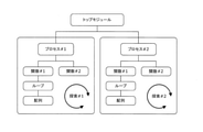
図6は、パラメータ最適化の対象となる処理システムの一例を示すブロック図である。図6に示す処理システム50は、全体としてFPGAからなり、並列展開されている複数の処理回路51に対して対象処理をループ展開して実行する処理システムである。
FIG. 6 is a block diagram showing an example of a processing system to be targeted for parameter optimization. The
処理システム50は、例えば図6に示すように、主な回路部として、振り分けられたパケットPKに対して予めループ展開された対象処理の一部を実行するN個(Nは2以上の整数)の処理回路(51)#1,#2,…,#Nと、同時に入力される複数フローのパケットPKを、並列展開されている処理回路#1,#2,…,#Nに振り分ける振分部52と、処理回路#1,#2,…,#Nで得られた処理結果を集約して出力する集約部53とを備えている。
As shown in FIG. 6, for example, the
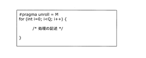
高位合成処理では、処理システム50の性能をチューニングするために、設計者が設定可能な設計パラメータが用意されている。性能チューニングに用いる設計パラメータの1つとして、ループ展開数がある。図7は、ループ展開数を指定したソースコードの一例である。
In the high-level synthesis process, design parameters that can be set by the designer are prepared in order to tune the performance of the
ループ展開とは、ループ処理における各イテレーションの処理を、並列展開した処理回路を用いて処理することで処理の高速化を図る手法である。図7の例では、ループ総数Q(Qは2以上の整数)回のループ処理に対してループ展開数M(Mは2以上の整数)を設定している。これは、例えば全部でQ回のループ処理が必要な対象処理において、1ループにMループ分の処理を展開してまとめて実行することにより、必要となるループ数をQ/M回に削減することを意味している。 Loop unrolling is a method for speeding up processing by processing each iteration in loop processing using a processing circuit expanded in parallel. In the example of FIG. 7, the loop unrolling number M (M is an integer of 2 or more) is set for the loop processing of the total number of loops Q (Q is an integer of 2 or more). This reduces the number of required loops to Q / M times, for example, by expanding the processing for M loops into one loop and executing them collectively in the target processing that requires Q loop processing in total. It means that.
このようにして、ループ展開数を任意の値に設定することで、処理回路の並列展開数を指定して処理システムを設計することができる。この場合、ループ展開数は増やせば増やすほど、処理システムの処理性能は向上するが、これに伴って処理システムにおけるリソース使用量も増加する。
従来、高位合成を用いた回路設計において、設計者が指定する設計パラメータ(例えば、ループ展開数など)の値を最適化する手法が提案されている(例えば、特許文献1など参照)。図8は、ソースコード記述から生成される解析木の一例である。この手法では、図8に示すような処理回路の動作を表す解析木を元に「回路あたりの処理レイテンシ」の最小化を目的として最適化を図っている。
By setting the number of loop unrolls to an arbitrary value in this way, it is possible to design a processing system by designating the number of parallel unrolls of the processing circuit. In this case, as the number of loop unrolls increases, the processing performance of the processing system improves, but the resource usage in the processing system also increases accordingly.
Conventionally, in circuit design using high-level synthesis, a method of optimizing the value of a design parameter (for example, the number of loop unrolls) specified by the designer has been proposed (see, for example, Patent Document 1). FIG. 8 is an example of a parsing tree generated from a source code description. In this method, optimization is attempted for the purpose of minimizing "processing latency per circuit" based on an analysis tree showing the operation of the processing circuit as shown in FIG.
一般に、高位合成において処理システムの性能をチューニングする際、処理システムの処理回路に関する「回路あたりの性能」を向上させると「回路あたりのリソース使用量」が増加する。このため、処理システムの「全体で使用可能なリソース量」が制限されており一定であるとすると、「回路あたりの性能」と「回路並列数」はトレードオフの関係にある。
しかしながら、前述したような従来技術では、処理回路に関する「回路あたりの性能」の最大化を目的としているため、「回路あたりの性能」と「回路並列数」のトレードオフを最適化することは困難であるという問題点があった。
In general, when tuning the performance of a processing system in high-level synthesis, improving the "performance per circuit" of the processing circuit of the processing system increases the "resource usage per circuit". Therefore, assuming that the "amount of resources that can be used as a whole" of the processing system is limited and constant, the "performance per circuit" and the "number of parallel circuits" are in a trade-off relationship.
However, it is difficult to optimize the trade-off between "performance per circuit" and "number of parallel circuits" because the conventional technology as described above aims at maximizing "performance per circuit" related to the processing circuit. There was a problem that it was.
通常、図6に示したように、並列展開した複数の処理回路を用いる場合、処理時間のオーバヘッドが発生する。例えば、入力パケットのフローに応じて処理回路内のステートを切り替えながら処理を行う場合が考えられる。このような場合には、ステート切り替えの所要時間に相当するオーバヘッドが発生するため、単位時間あたりに到着するフロー数が一定数以上の場合、「回路あたりの性能」を劣化させてでも「回路並列数」を増加させた方が、システム全体としては処理性能が高くなる場合があるからである。 Normally, as shown in FIG. 6, when a plurality of processing circuits expanded in parallel are used, an overhead of processing time occurs. For example, it is conceivable to perform processing while switching the state in the processing circuit according to the flow of the input packet. In such a case, an overhead corresponding to the time required for state switching occurs. Therefore, if the number of flows arriving per unit time is a certain number or more, even if the "performance per circuit" is deteriorated, "circuit parallelism" This is because the processing performance of the entire system may be higher if the number is increased.
本発明はこのような課題を解決するためのものであり、高位合成処理におけるループ展開数と回路並列数の最適な組み合わせを決定できるパラメータ最適化技術を提供することを目的としている。 The present invention is intended to solve such a problem, and an object of the present invention is to provide a parameter optimization technique capable of determining the optimum combination of the number of loop unrolls and the number of circuit parallels in high-level synthesis processing.
このような目的を達成するために、本発明にかかるパラメータ最適化装置は、複数の処理回路に対して対象処理をループ展開して実行する処理システムを、高位合成処理により回路設計する際、前記高位合成処理で用いる設計パラメータであるループ展開数と回路並列数の最適な組み合わせを決定するパラメータ最適化装置であって、前記設計パラメータの候補となる、前記ループ展開数と前記回路並列数の組み合わせを複数設定し、これら組み合わせごとに、前記高位合成処理により得られる合成回路を示す回路合成情報を生成する回路合成情報生成部と、前記回路合成情報ごとに、当該回路合成情報が示す合成回路に関する推定処理性能を算出し、最大の推定処理性能が得られた回路合成情報に基づいて、前記ループ展開数と前記回路並列数の最適な組み合わせを決定する最適パラメータ決定部とを備えている。 In order to achieve such an object, the parameter optimizer according to the present invention is described above when designing a processing system by loop unrolling and executing target processing for a plurality of processing circuits by high-level synthesis processing. A parameter optimizer that determines the optimum combination of the number of loop unrolls and the number of circuit parallels, which is a design parameter used in high-level synthesis processing, and is a combination of the number of loop unrolls and the number of circuit parallels, which is a candidate for the design parameter. For each of these combinations, a circuit synthesis information generation unit that generates circuit synthesis information indicating the synthesis circuit obtained by the high-level synthesis processing, and a synthesis circuit indicated by the circuit synthesis information for each of the circuit synthesis information. It is provided with an optimum parameter determination unit that calculates the estimated processing performance and determines the optimum combination of the loop unrolling number and the circuit parallel number based on the circuit synthesis information from which the maximum estimated processing performance is obtained.
また、本発明にかかる上記パラメータ最適化装置の一構成例は、前記回路合成情報生成部が、前記組み合わせを設定する際、前記ループ展開で展開すべきループの総数を示すループ総数に基づいて、前記ループ展開数を設定するようにしたものである。 Further, in one configuration example of the parameter optimization device according to the present invention, when the circuit synthesis information generation unit sets the combination, it is based on the total number of loops indicating the total number of loops to be expanded in the loop unrolling. The number of loop unrolls is set.
また、本発明にかかる上記パラメータ最適化装置の一構成例は、前記回路合成情報生成部が、前記組み合わせを設定する際、前記処理システムで使用可能なリソースを示すリソース制約に基づいて、前記回路並列数を設定するようにしたものである。 Further, in one configuration example of the parameter optimization device according to the present invention, when the circuit synthesis information generation unit sets the combination, the circuit is based on a resource constraint indicating resources that can be used in the processing system. The number of parallels is set.
また、本発明にかかる上記パラメータ最適化装置の一構成例は、前記最適パラメータ決定部が、前記推定処理性能を算出する際、前記回路合成情報と、前記対象処理で許容される処理遅延を示す遅延制約と、前記対象処理に対して並列的に入力されるデータの同時入力数とに基づいて、前記推定処理性能を算出するようにしたものである。 Further, in one configuration example of the parameter optimization device according to the present invention, when the optimum parameter determination unit calculates the estimation processing performance, the circuit synthesis information and the processing delay allowed in the target processing are shown. The estimated processing performance is calculated based on the delay constraint and the number of simultaneous inputs of data input in parallel with the target processing.
また、本発明にかかる上記パラメータ最適化装置の一構成例は、前記処理システムが、振り分けられたパケットに対して予めループ展開された前記対象処理の一部を実行する前記複数の処理回路と、同時に入力される複数フローのパケットを、前記複数の処理回路に対して振り分ける振分部と、前記複数の処理回路で得られた処理結果を集約して出力する集約部とを備えるものである。 Further, one configuration example of the parameter optimization device according to the present invention includes the plurality of processing circuits in which the processing system executes a part of the target processing previously loop-unrolled for the distributed packets. It includes a distribution unit that distributes packets of a plurality of flows that are input at the same time to the plurality of processing circuits, and an aggregation unit that aggregates and outputs the processing results obtained by the plurality of processing circuits.
また、本発明にかかる上記パラメータ最適化装置の一構成例は、前記複数の処理回路が、前記振分部から振り分けられたパケットのフローに応じて、当該パケットを処理するためのステートを切り替えるようにしたものである。 Further, in one configuration example of the parameter optimization device according to the present invention, the plurality of processing circuits switch states for processing the packet according to the flow of the packet distributed from the distribution unit. It is the one that was made.
また、本発明にかかるパラメータ最適化方法は、複数の処理回路に対して対象処理をループ展開して実行する処理システムを、高位合成処理により回路設計する際、前記高位合成処理で用いる設計パラメータであるループ展開数と回路並列数の最適な組み合わせを決定するパラメータ最適化装置で用いられるパラメータ最適化方法であって、回路合成情報生成部が、前記設計パラメータの候補となる、前記ループ展開数と前記回路並列数の組み合わせを複数設定し、これら組み合わせごとに、前記高位合成処理により得られる合成回路を示す回路合成情報を生成する回路合成情報生成ステップと、最適パラメータ決定部が、前記回路合成情報ごとに、当該回路合成情報が示す合成回路に関する推定処理性能を算出し、最大の推定処理性能が得られた回路合成情報に基づいて、前記ループ展開数と前記回路並列数の最適な組み合わせを決定する最適パラメータ決定ステップとを備えている。 Further, the parameter optimization method according to the present invention uses the design parameters used in the high-level synthesis processing when designing a circuit by loop-unrolling and executing the target processing for a plurality of processing circuits by the high-level synthesis processing. This is a parameter optimization method used in a parameter optimization device that determines the optimum combination of a certain number of loop unrolls and the number of circuit parallels, and the circuit synthesis information generator is a candidate for the design parameter, and the number of loop unrolls. A circuit synthesis information generation step for setting a plurality of combinations of the number of parallel circuits and generating circuit synthesis information indicating the synthesis circuit obtained by the high-level synthesis processing for each combination, and an optimum parameter determination unit are used for the circuit synthesis information. For each, the estimated processing performance of the synthesized circuit indicated by the circuit synthesis information is calculated, and the optimum combination of the loop unrolling number and the circuit parallel number is determined based on the circuit synthesis information obtained from which the maximum estimated processing performance is obtained. It is equipped with an optimum parameter determination step to be performed.
また、本発明にかかるプログラムは、コンピュータを、前述したいずれかのパラメータ最適化装置を構成する各部として機能させるためのプログラムである。 Further, the program according to the present invention is a program for making a computer function as each part constituting any of the above-mentioned parameter optimization devices.
本発明によれば、候補として複数設定されたループ展開数と回路並列数の組み合わせのうちから、推定処理性能が最も高い合成回路のループ展開数と回路並列数が最適な組み合わせとして選択されることになる。したがって、高位合成処理において処理システムの性能をチューニングする際に問題となる、処理回路に関する「回路あたりの性能」と「回路並列数」のトレードオフを最適化することが可能となる。また、高位合成処理において処理システムの性能をチューニングするのに要する工程期間を大幅に短縮することができ、チューニングに要する作業負担や作業コストを大幅に削減する可能となる。 According to the present invention, the number of loop unrolls and the number of circuit parallels of the synthetic circuit having the highest estimated processing performance are selected as the optimum combination from the combinations of the number of loop unrolls and the number of circuit parallels set as candidates. become. Therefore, it is possible to optimize the trade-off between "performance per circuit" and "number of parallel circuits" regarding the processing circuit, which is a problem when tuning the performance of the processing system in high-level synthesis processing. In addition, the process period required for tuning the performance of the processing system in the high-level synthesis process can be significantly shortened, and the work load and work cost required for tuning can be significantly reduced.
次に、本発明の一実施の形態について図面を参照して説明する。
[パラメータ最適化装置]
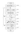
まず、図1を参照して、本実施の形態にかかるパラメータ最適化装置10について説明する。図1は、パラメータ最適化装置の構成を示すブロック図である。
このパラメータ最適化装置10は、全体としてサーバ装置などの情報処理装置(コンピュータ)からなり、複数の処理回路に対して対象処理をループ展開して実行する処理システムを、高位合成処理により回路設計する際、高位合成処理で用いるパラメータであるループ展開数と回路並列数の最適な組み合わせを決定する機能を有している。
Next, an embodiment of the present invention will be described with reference to the drawings.
[Parameter optimizer]
First, the
The
本実施の形態では、前述の図6に示したような、振り分けられたパケットを処理する複数の処理回路51が並列展開された処理システム50を対象として、高位合成処理で用いるループ展開数と回路並列数の最適な組み合わせを決定する場合について説明する。なお、パラメータ最適化の対象となる処理システムは、パケットを処理する処理システム50に限定されるものではなく、複数の処理回路に対して対象処理をループ展開して実行する処理システムであれば、同様にして本実施の形態を適用でき、同様の作用効果が得られる。
In the present embodiment, the number of loop unrolls and the circuit used in the high-level synthesis processing are targeted at the
処理システム50は、前述した図6の構成と同様に、主な回路部として、振り分けられたパケットPKに対して予めループ展開された対象処理の一部を実行するN個(Nは2以上の整数)の処理回路(51)#1,#2,…,#Nと、同時に入力される複数フローのパケットPKを、並列展開されている処理回路#1,#2,…,#Nに振り分ける振分部52と、処理回路#1,#2,…,#Nで得られた処理結果を集約して出力する集約部53とを備えているものとする。
Similar to the configuration of FIG. 6 described above, the
図1に示すように、パラメータ最適化装置10は、主な機能部として、回路合成情報生成部11、回路合成情報記憶部12、および最適パラメータ決定部13を備えている。これら機能部のうち、回路合成情報生成部11と最適パラメータ決定部13は、CPUとプログラムとが協働することにより実現されている。このプログラムは、外部装置や記録媒体(ともに図示せず)からパラメータ最適化装置10の記憶部(図示せず)に予め格納される。なお、プログラムは、記録媒体に記録して提供することもでき、通信ネットワークを介して提供することもできる。
As shown in FIG. 1, the
回路合成情報生成部11は、入力されたソースコード21に記述されている、ループ展開で展開すべきループの総数を示すループ総数Qと、リソース制約情報22で指定された、処理システム50で使用可能なリソースを示すリソース制約とに基づいて、設計パラメータの候補となる、ループ展開数M(Mは2以上の整数)と回路並列数Nとの組み合わせを複数設定する機能と、これら組み合わせごとに、当該組み合わせを適用した際に高位合成処理により得られる合成回路を示す回路合成情報23を生成して、回路合成情報記憶部12に登録する機能を有している。
The circuit synthesis
回路合成情報記憶部12は、ハードディスクや半導体メモリなど記憶装置からなり、回路合成情報生成部11で生成された回路合成情報23を記憶する機能を有している。
図2は、回路合成情報の構成例である。図2に示すように、回路合成情報23は、ループ展開数Mと回路並列数Nの組み合わせを示すパラメータと、合成回路の構成を示す処理サイクル数、動作周波数[MHz]、ステート切替サイクル数からなる合成結果情報とを含んでいる。これら回路合成情報23は、組み合わせを識別するためのIDが付与されて、回路合成情報記憶部12に登録されている。
The circuit synthesis
FIG. 2 is a configuration example of circuit synthesis information. As shown in FIG. 2, the
最適パラメータ決定部13は、遅延制約情報24で指定された処理システム50の対象処理で許容される処理遅延を示す遅延制約と、処理システム50の対象処理に対して並列的に同時に入力されうるパケット(データ)のフロー数を示す同時アクセスフロー数(同時入力数)25とに基づいて、回路合成情報記憶部12に登録されている回路合成情報23ごとに、当該回路合成情報23が示す合成回路から得られる推定処理性能Pを算出する機能と、これら推定処理性能のうち最大推定処理性能Pmaxが得られた回路合成情報23に基づいて、ループ展開数Mと回路並列数Nの最適な組み合わせを決定し、最適パラメータ26として出力する機能とを有している。
The optimum
[回路合成情報生成部]
次に、図1を参照して、回路合成情報生成部11の詳細について説明する。
図1に示すように、回路合成情報生成部11は、主な処理部として、パラメータ設定部11A、高位合成部11B、回路並列数算出部11C、および情報登録部11Dを備えている。
[Circuit synthesis information generator]
Next, the details of the circuit synthesis
As shown in FIG. 1, the circuit synthesis
パラメータ設定部11Aは、ソースコード21で指定されたループ総数Qに基づいて、候補となるループ展開数Mを複数設定する機能を有している。
高位合成部11Bは、パラメータ設定部11Aが設定したループ展開数Mごとに、当該ループ展開数Mを適用した際に得られる合成回路を、高位合成処理により合成する機能を有している。
The
The high-
回路並列数算出部11Cは、リソース制約情報22で指定された処理システム50で使用可能なリソースを示すリソース制約と、高位合成部11Bで合成された合成回路のリソース使用量とに基づいて、合成回路ごとに候補となる回路並列数Nを算出して設定する機能を有している。
情報登録部11Dは、候補として設定されたループ展開数Mと回路並列数Nとの組み合わせに、組み合わせを識別するためのIDと、対応する合成回路の構成を示す合成結果情報とを付与し、得られた回路合成情報23を回路合成情報記憶部12に登録する機能を有している。
The circuit parallel
The
[最適パラメータ決定部]
次に、図1を参照して、最適パラメータ決定部13の詳細について説明する。
図1に示すように、最適パラメータ決定部13は、主な処理部として、性能推定部13A、性能比較部13B、最適パラメータ記憶部13C、およびパラメータ出力部13Dを備えている。
[Optimal parameter determination unit]
Next, the details of the optimum
As shown in FIG. 1, the optimum
性能推定部13Aは、回路合成情報記憶部12に登録されている回路合成情報23ごとに、回路合成情報23に含まれるループ展開数Mと回路並列数Nとの組み合わせを適用した場合に得られる処理システム50の性能値である推定処理性能Pを算出する機能を有している。
The
性能比較部13Bは、性能推定部13Aで算出された推定処理性能Pを最適パラメータ記憶部13Cで記憶している最大推定処理性能Pmaxと比較する機能と、PがPmaxより大きい場合には、PmaxをPで更新するとともに、Pと対応するループ展開数Mと回路並列数Nとの組み合わせを最適パラメータとして最適パラメータ記憶部13Cに保存する機能とを有している。
The
パラメータ出力部13Dは、回路合成情報記憶部12に登録されているすべての回路合成情報23に関するPとPmaxとの比較が完了した後、最適パラメータ記憶部13Cに保存されている最適パラメータを取得して出力する機能を有している。
The
[本実施の形態の動作]
次に、本実施の形態にかかるパラメータ最適化装置10の動作について説明する。
[Operation of this embodiment]
Next, the operation of the
[回路合成情報生成動作]
まず、図3を参照して、回路合成情報生成部11の回路合成情報生成動作について説明する。図3は、回路合成情報生成処理を示すフローチャートである。
[Circuit synthesis information generation operation]
First, the circuit synthesis information generation operation of the circuit synthesis
まず、パラメータ設定部11Aは、例えば図7に示したようなソースコード21に含まれるfor文の記述からループ総数Qを取得する(ステップ100)。
続いて、パラメータ設定部11Aは、ループ展開数Miを1~Qの範囲で1ずつ変化させて設定するため、まず、変数iを1で初期化し(ステップ101)、iの値をループ展開数Miに設定する(ステップ102)。
First, the
Subsequently, the
次に、高位合成部11Bは、パラメータ設定部11Aが設定したループ展開数Miを適用した際に得られる合成回路を、高位合成コンパラを用いてソースコード21から合成する(ステップ103)。
Next, the high-
続いて、回路並列数算出部11Cは、高位合成部11Bで合成された合成回路に関する合成結果情報から、処理回路51あたりのリソース使用量Siを取得し(ステップ104)、このリソース使用量Siと、リソース制約情報22で指定された処理システム50で使用可能なリソースを示すリソース制約Smaxとに基づいて、ループ展開数Miの合成回路に関する回路並列数Niを算出する(ステップ105)。
Subsequently, the circuit parallel
この際、Niについては、Si×NiがSmax以下となる最大の数をNiとして選択する方法が考えられるが、これに限定されるものではない。例えば、ソースコード21から合成される合成回路以外に、並列化に必要な周辺回路などのリソースに関する使用リソース量を加味してNiを算出してもよい。
At this time, for N i , a method of selecting the maximum number in which S i × N i is S max or less can be considered as N i , but the method is not limited to this. For example, in addition to the synthetic circuit synthesized from the
この後、情報登録部11Dは、得られたループ展開数Miと回路並列数Niとの組み合わせに、組み合わせを識別するためのIDと、対応する合成回路の構成を示す合成結果情報とを付与し、得られた回路合成情報23を回路合成情報記憶部12に登録する(ステップ106)。
After that, the
次に、パラメータ設定部11Aは、変数iがループ総数Qに到達したか確認し(ステップ107)、iがQに到達していない場合(ステップ107:NO)、iをインクリメント(i=i+1)した後(ステップ108)、ステップ102へ戻る。
一方、iがQに到達した場合(ステップ107:YES)、一連の回路合成情報生成処理を終了する。
Next, the
On the other hand, when i reaches Q (step 107: YES), a series of circuit synthesis information generation processes are terminated.
[最適パラメータ決定動作]
次に、図4を参照して、最適パラメータ決定部13の最適パラメータ決定動作について説明する。図4は、最適パラメータ決定処理を示すフローチャートである。
[Optimal parameter determination operation]
Next, the optimum parameter determination operation of the optimum
まず、性能推定部13Aは、最適パラメータ記憶部13Cで記憶する最大推定処理性能Pmaxをゼロで初期化した後(ステップ110)、回路合成情報記憶部12から未選択の回路合成情報23を1つ選択し(ステップ111)、選択した回路合成情報23に含まれるループ展開数Mと回路並列数Nとの組み合わせを適用した場合に得られる処理システム50の性能値である推定処理性能Pを算出する(ステップ112)。推定処理性能Pの算出方法については後述する。
First, the
性能比較部13Bは、性能推定部13Aで算出された推定処理性能Pを、最適パラメータ記憶部13Cで記憶している最大推定処理性能Pmaxと比較し(ステップ113)、PがPmax以下の場合には(ステップ113:NO)、ステップ111へ戻る。
一方、PがPmaxより大きい場合(ステップ113:YES)、性能比較部13Bは、PmaxをPで更新するとともに(ステップ114)、Pと対応するループ展開数Mと回路並列数Nとの組み合わせを最適パラメータ26として最適パラメータ記憶部13Cに保存する(ステップ115)。
The
On the other hand, when P is larger than P max (step 113: YES), the
この後、パラメータ出力部13Dは、回路合成情報記憶部12に登録されているすべての回路合成情報23の選択が完了したか確認し(ステップ116)、未完了の場合には(ステップ116:NO)、ステップ111へ戻る。
一方、すべての回路合成情報23の選択が完了した場合(ステップ116:YES)、パラメータ出力部13Dは、最適パラメータ記憶部13Cに保存されている最適パラメータ26を取得して出力し(ステップ117)、一連の最適パラメータ決定処理を終了する。
After that, the
On the other hand, when the selection of all the
なお、性能比較部13Bが、最適パラメータ記憶部13Cに最適パラメータを保存する際、選択した回路合成情報23に含まれるループ展開数Mと回路並列数Nとの組み合わせを示すIDを保存してもよい。また、パラメータ出力部13Dが最適パラメータを出力する際、ループ展開数Mと回路並列数Nとの組み合わせを示すIDを出力してもよい。
When the
[推定処理性能算出方法]
次に、図5を参照して、性能推定部13Aにおける推定処理性能算出方法について説明する。図5は、一般的な待ち行列システムを示す概念図である。
[Estimated processing performance calculation method]
Next, with reference to FIG. 5, the estimation processing performance calculation method in the
本推定手法では、入力パケットがランダムに到着する処理システム50における処理遅延を確率論的に評価するために、最適化の対象となる処理システム50を、図5に示すような待ち行列システム30として捉え、待ち行列理論に基づく理論式を用いて性能を推定する。ここでは、推定処理性能を「遅延制約を満たす最大の入力レート」と定義する。また、遅延制約は、遅延制約情報24により「遅延がa秒以内である確率がb%以上」であるというように与えられるものとする。
In this estimation method, in order to probabilistically evaluate the processing delay in the
図5に示すように、待ち行列システム30は、複数のサービス窓口31と待ち行列から構成されている。この待ち行列システムを図6の処理システム50と対比させると、外部から入力されるパケットPKがランダムに到着する要求REQに対応し、並列展開された処理回路51がサービス窓口31に対応し、振分部52においてパケットを格納するためのキュー(図示せず)が待ち行列32に対応する。なお、キューはレジスタあるいはメモリを用いて実装される。
As shown in FIG. 5, the
次に、性能推定に用いる推定式について説明する。
待ち行列理論に基づいて対象とする待ち行列システムにおける各要求の待ち時間を確率論的に評価するための理論式は、次の式(1)で表される。

The theoretical formula for probabilistically evaluating the waiting time of each request in the target queue system based on the queuing theory is expressed by the following formula (1).
式(1)において、Cは待ち行列システム30における、各要求REQの待ち時間が許容値tを超える確率を表す。また、nはサービス窓口数を表し、Eは呼量すなわち要求REQの量に関する尺度を表している。また、AHTは要求REQの1件あたりのサービス時間を表し、Bは対象とするシステムが呼損系であると仮定した場合の呼損率を表している。ここで、呼損系とは、サービス窓口31が全て使用中の状態で新たな要求REQが到着した場合、その要求REQを待ち行列に並ばせるのではなく破棄する機能を有するシステムを指す。
In the equation (1), C represents the probability that the waiting time of each request RQ in the
式(1)のうち、呼損率Bについては、次の式(2)を用いて算出される。

式(2)のうち、呼量Eについては、次の式(3)を用いて算出される。ここで、λは単位時間あたりの要求到着数を表す。その他の変数の定義は式(1)と同様である。
![]()
![]()
また、遅延入力レートRと要求到着数λの関係は式(4)のように表される。ここで、Lはパケット長を表す。
![]()
![]()
これらをまとめると、遅延制約が「遅延がa秒以内である確率がb%以上」である場合、許容値tの値をa秒に設定して、遅延入力レートRすなわち呼量Eを増加させていくことにより、確率Cの値がb%を維持する最大入力レートRmaxを求める。求めたRmaxが待ち行列システム30に関する推定処理性能Pとなる。
To summarize these, when the delay constraint is "the probability that the delay is within a second is b% or more", the value of the allowable value t is set to a second, and the delay input rate R, that is, the call volume E is increased. By doing so, the maximum input rate R max at which the value of the probability C maintains b% is obtained. The obtained R max is the estimated processing performance P for the
[AHT算出方法]
続いて、AHTの算出方法を説明する。
パラメータ最適化の対象とする処理システム50は、各処理回路51において、入力パケットのフローに応じて処理回路51内のステートを切り替えながら処理することを特徴とする。このため、現在処理中のパケットのフローと次に入力されるパケットのフローが異なる場合、処理回路51内のステートの切り替え処理が発生し、処理時間のオーバヘッドが発生する。
[AHT calculation method]
Subsequently, a method of calculating AHT will be described.
The
また、同一処理回路51に同時に入力されるフロー数が増えれば増えるほど、現在処理中のパケットのフローと次に入力されるパケットのフローが異なる確率は高くなる。したがって、同一処理回路51に同時に入力されるフロー数が増えれば増えるほど、処理回路51内のステート切り替えによる処理時間のオーバヘッドが発生する確率が高くなる。
以上を考慮して、本発明では、ステート切り替えによる処理時間のオーバヘッド発生確率を加味した期待値としてAHTを算出する。
Further, as the number of flows simultaneously input to the
In consideration of the above, in the present invention, the AHT is calculated as an expected value in consideration of the probability of occurrence of overhead in the processing time due to state switching.
次の式(5)は、AHTの算出式である。
![]()
![]()
式(5)において、Psameは、入力パケットのフローが1つ前の入力パケットのフローと同じ確率を表す。また、AHTαは、ステート切り替えが発生しない場合のパケットあたりの処理時間を表し、AHTβは、ステート切り替えが発生する場合のパケットあたりの処理時間を表している。AHTαとAHTβは、回路合成情報記憶部12に保持された情報から算出する。
In the equation (5), P same represents the probability that the flow of the input packet is the same as the flow of the previous input packet. Further, AHT α represents the processing time per packet when state switching does not occur, and AHT β represents the processing time per packet when state switching occurs. AHT α and AHT β are calculated from the information held in the circuit synthesis
式(5)のうち、Psameは、次の式(6)を用いて算出される。

式(6)において、サービス窓口数nは、回路並列数とする。また、Nflowは、システムに対する同時アクセスフロー数を表す。ここでは、処理システム50に入力されるパケットのフローはランダムであり、各フローの到着確率が1/Nflowであるという仮定の元でPsameを算出しているが、フローごとに異なる到着確率を仮定してPsameを算出してもよい。
In the equation (6), the number of service counters n is the number of parallel circuits. Further, N flow represents the number of simultaneous access flows to the system. Here, the flow of the packet input to the
[本実施の形態の効果]
このように、本実施の形態は、回路合成情報生成部11が、パラメータの候補としてループ展開数Mと回路並列数Nの組み合わせを複数設定して、これら組み合わせごとに、高位合成処理により得られる合成回路を示す回路合成情報23を生成し、最適パラメータ決定部13が、生成された回路合成情報23ごとに、当該回路合成情報23が示す合成回路に関する推定処理性能Pを算出し、最大の推定処理性能Pmaxが得られた回路合成情報23に基づいて、ループ展開数Mと回路並列数Nの最適な組み合わせを決定するようにしたものである。
[Effect of this embodiment]
As described above, in this embodiment, the circuit synthesis
これにより、候補として複数設定されたループ展開数Mと回路並列数Nの組み合わせのうちから、推定処理性能Pが最も高い推定処理性能Pmaxである合成回路のループ展開数Mと回路並列数Nが最適な組み合わせとして選択されることになる。したがって、高位合成処理において処理システム50の性能をチューニングする際に問題となる、処理回路51に関する「回路あたりの性能」と「回路並列数」のトレードオフを最適化することが可能となる。また、高位合成処理において処理システム50の性能をチューニングするのに要する工程期間を大幅に短縮することができ、チューニングに要する作業負担や作業コストを大幅に削減する可能となる。
As a result, among the combinations of the loop unrolling number M and the circuit parallel number N set as multiple candidates, the loop unrolling number M and the circuit parallel number N of the synthetic circuit having the highest estimated processing performance P max . Will be selected as the optimal combination. Therefore, it is possible to optimize the trade-off between "performance per circuit" and "number of parallel circuits" regarding the
また、本実施の形態において、回路合成情報生成部11が、組み合わせを設定する際、ループ展開で展開すべきループの総数を示すループ総数に基づいて、ループ展開数を設定するようにしてもよい。
また、本実施の形態において、回路合成情報生成部11が、処理システムで使用可能なリソースを示すリソース制約に基づいて、回路並列数を設定するようにしてもよい。
これにより、規定のループ総数およびリソース制約を持つ処理システム50に対して、過不足のない最適なループ展開数および回路並列数を特定することができる。
Further, in the present embodiment, when the circuit synthesis
Further, in the present embodiment, the circuit synthesis
As a result, it is possible to specify the optimum number of loop unrolls and the number of parallel circuits for the
また、本実施の形態において、最適パラメータ決定部13が、推定処理性能Pを算出する際、回路合成情報23と、対象処理で許容される処理遅延を示す遅延制約と、対象処理に対して並列的に入力されるデータの同時入力数とに基づいて、推定処理性能Pを算出するようにしてもよい。
これにより、入力されたパケットのフローに応じて処理時間が異なる場合であっても、外部から与えられる各フローの到着確率を加味した最適化を図ることができ、実動作環境を反映した回路性能の最適化が可能となる。
Further, in the present embodiment, when the optimum
As a result, even if the processing time differs depending on the flow of the input packet, optimization can be achieved in consideration of the arrival probability of each flow given from the outside, and the circuit performance that reflects the actual operating environment. Can be optimized.
[実施の形態の拡張]
以上、実施形態を参照して本発明を説明したが、本発明は上記実施形態に限定されるものではない。本発明の構成や詳細には、本発明のスコープ内で当業者が理解しうる様々な変更をすることができる。
[Extension of embodiment]
Although the present invention has been described above with reference to the embodiments, the present invention is not limited to the above embodiments. Various changes that can be understood by those skilled in the art can be made to the structure and details of the present invention within the scope of the present invention.
10…パラメータ最適化装置、11…回路合成情報生成部、11A…パラメータ設定部、11B…高位合成部、11C…回路並列数算出部、11D…情報登録部、12…回路合成情報記憶部、13…最適パラメータ決定部、13A…性能推定部、13B…性能比較部、13C…最適パラメータ記憶部、13D…パラメータ出力部、21…ソースコード、22…リソース制約情報、23…回路合成情報、24…遅延制約情報、25…同時アクセスフロー数、26…最適パラメータ。 10 ... Parameter optimizer, 11 ... Circuit synthesis information generation unit, 11A ... Parameter setting unit, 11B ... High-level synthesis unit, 11C ... Circuit parallel number calculation unit, 11D ... Information registration unit, 12 ... Circuit synthesis information storage unit, 13 ... Optimal parameter determination unit, 13A ... Performance estimation unit, 13B ... Performance comparison unit, 13C ... Optimal parameter storage unit, 13D ... Parameter output unit, 21 ... Source code, 22 ... Resource constraint information, 23 ... Circuit synthesis information, 24 ... Delay constraint information, 25 ... Number of simultaneous access flows, 26 ... Optimal parameters.
Claims (8)
前記設計パラメータの候補となる、前記ループ展開数と前記回路並列数の組み合わせを複数設定し、これら組み合わせごとに、前記高位合成処理により得られる合成回路を示す回路合成情報を生成する回路合成情報生成部と、
前記回路合成情報ごとに、当該回路合成情報が示す合成回路に関する推定処理性能を算出し、最大の推定処理性能が得られた回路合成情報に基づいて、前記ループ展開数と前記回路並列数の最適な組み合わせを決定する最適パラメータ決定部と
を備えることを特徴とするパラメータ最適化装置。 When designing a processing system that loop-unrolls and executes target processing for multiple processing circuits by high-level synthesis processing, the optimum combination of the number of loop unrolling and the number of circuit parallels, which are the design parameters used in the high-level synthesis processing. It is a parameter optimizer that determines
A plurality of combinations of the number of loop unrolls and the number of parallel circuits, which are candidates for the design parameters, are set, and circuit synthesis information generation that generates circuit synthesis information indicating the synthesis circuit obtained by the high-level synthesis process is generated for each of these combinations. Department and
For each circuit synthesis information, the estimation processing performance of the synthesis circuit indicated by the circuit synthesis information is calculated, and the optimum number of loop unrolls and the number of circuit parallels is optimized based on the circuit synthesis information from which the maximum estimation processing performance is obtained. A parameter optimization device including an optimum parameter determination unit for determining various combinations.
前記回路合成情報生成部は、前記組み合わせを設定する際、前記ループ展開で展開すべきループの総数を示すループ総数に基づいて、前記ループ展開数を設定することを特徴とするパラメータ最適化装置。 In the parameter optimization apparatus according to claim 1,
The circuit synthesis information generation unit is a parameter optimization device, characterized in that, when setting the combination, the loop unrolling number is set based on the total number of loops indicating the total number of loops to be expanded in the loop unrolling.
前記回路合成情報生成部は、前記組み合わせを設定する際、前記処理システムで使用可能なリソースを示すリソース制約に基づいて、前記回路並列数を設定することを特徴とするパラメータ最適化装置。 In the parameter optimization apparatus according to claim 1 or 2.
The circuit synthesis information generation unit is a parameter optimization device characterized in that when setting the combination, the number of parallel circuits is set based on a resource constraint indicating resources that can be used in the processing system.
前記最適パラメータ決定部は、前記推定処理性能を算出する際、前記回路合成情報と、前記対象処理で許容される処理遅延を示す遅延制約と、前記対象処理に対して並列的に入力されるデータの同時入力数とに基づいて、前記推定処理性能を算出することを特徴とするパラメータ最適化装置。 In the parameter optimization apparatus according to any one of claims 1 to 3.
When calculating the estimated processing performance, the optimum parameter determining unit includes the circuit synthesis information, a delay constraint indicating a processing delay allowed in the target processing, and data input in parallel with the target processing. A parameter optimizer for calculating the estimated processing performance based on the number of simultaneous inputs of.
前記処理システムは、
振り分けられたパケットに対して予めループ展開された前記対象処理の一部を実行する前記複数の処理回路と、
同時に入力される複数フローのパケットを、前記複数の処理回路に対して振り分ける振分部と、
前記複数の処理回路で得られた処理結果を集約して出力する集約部とを備える
ことを特徴とするパラメータ最適化装置。 In the parameter optimization apparatus according to any one of claims 1 to 4.
The processing system is
The plurality of processing circuits that execute a part of the target processing that has been loop-unrolled in advance for the distributed packets, and the plurality of processing circuits.
A distribution unit that distributes packets of multiple flows input at the same time to the plurality of processing circuits, and
A parameter optimization device including an aggregation unit that aggregates and outputs the processing results obtained by the plurality of processing circuits.
前記複数の処理回路は、前記振分部から振り分けられたパケットのフローに応じて、当該パケットを処理するためのステートを切り替えることを特徴とするパラメータ最適化装置。 In the parameter optimization apparatus according to claim 5,
The plurality of processing circuits are parameter optimization devices characterized in that the state for processing the packet is switched according to the flow of the packet distributed from the distribution unit.
回路合成情報生成部が、前記設計パラメータの候補となる、前記ループ展開数と前記回路並列数の組み合わせを複数設定し、これら組み合わせごとに、前記高位合成処理により得られる合成回路を示す回路合成情報を生成する回路合成情報生成ステップと、
最適パラメータ決定部が、前記回路合成情報ごとに、当該回路合成情報が示す合成回路に関する推定処理性能を算出し、最大の推定処理性能が得られた回路合成情報に基づいて、前記ループ展開数と前記回路並列数の最適な組み合わせを決定する最適パラメータ決定ステップと
を備えることを特徴とするパラメータ最適化方法。 When designing a processing system that loop-unrolls and executes target processing for multiple processing circuits by high-level synthesis processing, the optimum combination of the number of loop unrolling and the number of circuit parallels, which are the design parameters used in the high-level synthesis processing. It is a parameter optimization method used in the parameter optimization device that determines
The circuit synthesis information generation unit sets a plurality of combinations of the loop unrolling number and the circuit parallel number, which are candidates for the design parameter, and for each of these combinations, circuit synthesis information indicating the synthesis circuit obtained by the high-level synthesis processing. And the circuit synthesis information generation step to generate
The optimum parameter determination unit calculates the estimation processing performance of the synthesis circuit indicated by the circuit synthesis information for each circuit synthesis information, and based on the circuit synthesis information for which the maximum estimation processing performance is obtained, the number of loop unrolls and the number of loop unrolls. A parameter optimization method comprising the optimum parameter determination step for determining the optimum combination of the number of parallel circuits.
Priority Applications (3)
| Application Number | Priority Date | Filing Date | Title |
|---|---|---|---|
| JP2018112515A JP6996431B2 (en) | 2018-06-13 | 2018-06-13 | Parameter optimizer, method, and program |
| PCT/JP2019/020104 WO2019239820A1 (en) | 2018-06-13 | 2019-05-21 | Parameter optimization device, method and program |
| US17/251,739 US11720080B2 (en) | 2018-06-13 | 2019-05-21 | Parameter optimization device, method and program |
Applications Claiming Priority (1)
| Application Number | Priority Date | Filing Date | Title |
|---|---|---|---|
| JP2018112515A JP6996431B2 (en) | 2018-06-13 | 2018-06-13 | Parameter optimizer, method, and program |
Publications (2)
| Publication Number | Publication Date |
|---|---|
| JP2019215697A JP2019215697A (en) | 2019-12-19 |
| JP6996431B2 true JP6996431B2 (en) | 2022-01-17 |
Family
ID=68842519
Family Applications (1)
| Application Number | Title | Priority Date | Filing Date |
|---|---|---|---|
| JP2018112515A Active JP6996431B2 (en) | 2018-06-13 | 2018-06-13 | Parameter optimizer, method, and program |
Country Status (3)
| Country | Link |
|---|---|
| US (1) | US11720080B2 (en) |
| JP (1) | JP6996431B2 (en) |
| WO (1) | WO2019239820A1 (en) |
Families Citing this family (1)
| Publication number | Priority date | Publication date | Assignee | Title |
|---|---|---|---|---|
| JP7791438B2 (en) | 2022-06-09 | 2025-12-24 | 富士通株式会社 | Conversion program and conversion processing method |
Citations (2)
| Publication number | Priority date | Publication date | Assignee | Title |
|---|---|---|---|---|
| JP2002269162A (en) | 2001-03-08 | 2002-09-20 | Nec Eng Ltd | Action synthesizing method |
| WO2018066074A1 (en) | 2016-10-04 | 2018-04-12 | 三菱電機株式会社 | Information processing device, information processing method, and information processing program |
Family Cites Families (7)
| Publication number | Priority date | Publication date | Assignee | Title |
|---|---|---|---|---|
| US5367651A (en) * | 1992-11-30 | 1994-11-22 | Intel Corporation | Integrated register allocation, instruction scheduling, instruction reduction and loop unrolling |
| WO2010113330A2 (en) * | 2009-03-31 | 2010-10-07 | Nec Corporation | Method and apparatus for design space exploration in high level synthesis |
| JP6242170B2 (en) * | 2013-11-13 | 2017-12-06 | 三菱電機株式会社 | Circuit design support apparatus and program |
| US10326448B2 (en) * | 2013-11-15 | 2019-06-18 | Scientific Concepts International Corporation | Code partitioning for the array of devices |
| CN105447285B (en) * | 2016-01-20 | 2018-11-30 | 杭州菲数科技有限公司 | A method of improving OpenCL hardware execution efficiency |
| JP6776069B2 (en) * | 2016-09-08 | 2020-10-28 | 東芝情報システム株式会社 | RTL optimization system and RTL optimization program |
| US10380313B1 (en) * | 2016-12-08 | 2019-08-13 | Xilinx, Inc. | Implementation and evaluation of designs for heterogeneous computing platforms with hardware acceleration |
-
2018
- 2018-06-13 JP JP2018112515A patent/JP6996431B2/en active Active
-
2019
- 2019-05-21 US US17/251,739 patent/US11720080B2/en active Active
- 2019-05-21 WO PCT/JP2019/020104 patent/WO2019239820A1/en not_active Ceased
Patent Citations (2)
| Publication number | Priority date | Publication date | Assignee | Title |
|---|---|---|---|---|
| JP2002269162A (en) | 2001-03-08 | 2002-09-20 | Nec Eng Ltd | Action synthesizing method |
| WO2018066074A1 (en) | 2016-10-04 | 2018-04-12 | 三菱電機株式会社 | Information processing device, information processing method, and information processing program |
Also Published As
| Publication number | Publication date |
|---|---|
| JP2019215697A (en) | 2019-12-19 |
| US20210116882A1 (en) | 2021-04-22 |
| WO2019239820A1 (en) | 2019-12-19 |
| US11720080B2 (en) | 2023-08-08 |
Similar Documents
| Publication | Publication Date | Title |
|---|---|---|
| US6826733B2 (en) | Parameter variation tolerant method for circuit design optimization | |
| KR100998798B1 (en) | Critical Estimation Systems and Methods in Statistical Timing Analysis | |
| Wolkotte et al. | Fast, accurate and detailed NoC simulations | |
| US20120239372A1 (en) | Efficient discrete event simulation using priority queue tagging | |
| EP3908920B1 (en) | Optimizing hardware fifo instructions | |
| US8407654B2 (en) | Glitch power reduction | |
| JP2006505061A (en) | Processor pipeline design method and design system | |
| WO2020162205A1 (en) | Optimization device, method, and program | |
| JP6996431B2 (en) | Parameter optimizer, method, and program | |
| JP2003150657A (en) | High-level synthesis method and high-level synthesis apparatus | |
| US10380287B1 (en) | Systems and methods for modifying a balanced clock structure | |
| Gokbayrak et al. | Online surrogate problem methodology for stochastic discrete resource allocation problems | |
| Fujiwara et al. | A high-level synthesis algorithm for FPGA designs optimizing critical path with interconnection-delay and clock-skew consideration | |
| Indrusiak et al. | Fast simulation of networks-on-chip with priority-preemptive arbitration | |
| Jeż | A universal randomized packet scheduling algorithm | |
| CN117217759A (en) | Transaction execution method, device and storage medium based on DAG blockchain system | |
| Puranik et al. | Key-value store using high level synthesis flow for securities trading system | |
| Ferreira et al. | Moments of losses during busy-periods of regular and nonpreemptive oscillating MX/G/1/n systems | |
| Hall et al. | Using m/g/l queueing models with vacations to analyze virtualized logic computations | |
| US20210406915A1 (en) | Mobile wireless customer micro-care apparatus and method | |
| US20160103710A1 (en) | Scheduling device | |
| CN117597673A (en) | Data processing apparatus and method for processing stagnant data | |
| Ewetz et al. | Fast clock skew scheduling based on sparse-graph algorithms | |
| KR20190070449A (en) | Parallel sceduling method and apparatus | |
| Ranade | The delay sequence argument |
Legal Events
| Date | Code | Title | Description |
|---|---|---|---|
| A621 | Written request for application examination |
Free format text: JAPANESE INTERMEDIATE CODE: A621 Effective date: 20201006 |
|
| TRDD | Decision of grant or rejection written | ||
| A01 | Written decision to grant a patent or to grant a registration (utility model) |
Free format text: JAPANESE INTERMEDIATE CODE: A01 Effective date: 20211116 |
|
| A61 | First payment of annual fees (during grant procedure) |
Free format text: JAPANESE INTERMEDIATE CODE: A61 Effective date: 20211129 |
|
| R150 | Certificate of patent or registration of utility model |
Ref document number: 6996431 Country of ref document: JP Free format text: JAPANESE INTERMEDIATE CODE: R150 |
|
| S533 | Written request for registration of change of name |
Free format text: JAPANESE INTERMEDIATE CODE: R313533 |
|
| R350 | Written notification of registration of transfer |
Free format text: JAPANESE INTERMEDIATE CODE: R350 |