JP6974635B2 - Semiconductor manufacturing measurement and processing control - Google Patents
Semiconductor manufacturing measurement and processing control Download PDFInfo
- Publication number
- JP6974635B2 JP6974635B2 JP2020569886A JP2020569886A JP6974635B2 JP 6974635 B2 JP6974635 B2 JP 6974635B2 JP 2020569886 A JP2020569886 A JP 2020569886A JP 2020569886 A JP2020569886 A JP 2020569886A JP 6974635 B2 JP6974635 B2 JP 6974635B2
- Authority
- JP
- Japan
- Prior art keywords
- measurement
- spectrum
- tool
- semiconductor wafer
- manufacturing
- Prior art date
- Legal status (The legal status is an assumption and is not a legal conclusion. Google has not performed a legal analysis and makes no representation as to the accuracy of the status listed.)
- Active
Links
Images


Classifications
-
- G—PHYSICS
- G06—COMPUTING OR CALCULATING; COUNTING
- G06N—COMPUTING ARRANGEMENTS BASED ON SPECIFIC COMPUTATIONAL MODELS
- G06N20/00—Machine learning
-
- G—PHYSICS
- G01—MEASURING; TESTING
- G01B—MEASURING LENGTH, THICKNESS OR SIMILAR LINEAR DIMENSIONS; MEASURING ANGLES; MEASURING AREAS; MEASURING IRREGULARITIES OF SURFACES OR CONTOURS
- G01B11/00—Measuring arrangements characterised by the use of optical techniques
- G01B11/02—Measuring arrangements characterised by the use of optical techniques for measuring length, width or thickness
- G01B11/06—Measuring arrangements characterised by the use of optical techniques for measuring length, width or thickness for measuring thickness ; e.g. of sheet material
-
- G—PHYSICS
- G03—PHOTOGRAPHY; CINEMATOGRAPHY; ANALOGOUS TECHNIQUES USING WAVES OTHER THAN OPTICAL WAVES; ELECTROGRAPHY; HOLOGRAPHY
- G03F—PHOTOMECHANICAL PRODUCTION OF TEXTURED OR PATTERNED SURFACES, e.g. FOR PRINTING, FOR PROCESSING OF SEMICONDUCTOR DEVICES; MATERIALS THEREFOR; ORIGINALS THEREFOR; APPARATUS SPECIALLY ADAPTED THEREFOR
- G03F7/00—Photomechanical, e.g. photolithographic, production of textured or patterned surfaces, e.g. printing surfaces; Materials therefor, e.g. comprising photoresists; Apparatus specially adapted therefor
- G03F7/70—Microphotolithographic exposure; Apparatus therefor
- G03F7/70483—Information management; Active and passive control; Testing; Wafer monitoring, e.g. pattern monitoring
- G03F7/70491—Information management, e.g. software; Active and passive control, e.g. details of controlling exposure processes or exposure tool monitoring processes
- G03F7/705—Modelling or simulating from physical phenomena up to complete wafer processes or whole workflow in wafer productions
-
- G—PHYSICS
- G03—PHOTOGRAPHY; CINEMATOGRAPHY; ANALOGOUS TECHNIQUES USING WAVES OTHER THAN OPTICAL WAVES; ELECTROGRAPHY; HOLOGRAPHY
- G03F—PHOTOMECHANICAL PRODUCTION OF TEXTURED OR PATTERNED SURFACES, e.g. FOR PRINTING, FOR PROCESSING OF SEMICONDUCTOR DEVICES; MATERIALS THEREFOR; ORIGINALS THEREFOR; APPARATUS SPECIALLY ADAPTED THEREFOR
- G03F7/00—Photomechanical, e.g. photolithographic, production of textured or patterned surfaces, e.g. printing surfaces; Materials therefor, e.g. comprising photoresists; Apparatus specially adapted therefor
- G03F7/70—Microphotolithographic exposure; Apparatus therefor
- G03F7/70483—Information management; Active and passive control; Testing; Wafer monitoring, e.g. pattern monitoring
- G03F7/70605—Workpiece metrology
- G03F7/70616—Monitoring the printed patterns
-
- G—PHYSICS
- G03—PHOTOGRAPHY; CINEMATOGRAPHY; ANALOGOUS TECHNIQUES USING WAVES OTHER THAN OPTICAL WAVES; ELECTROGRAPHY; HOLOGRAPHY
- G03F—PHOTOMECHANICAL PRODUCTION OF TEXTURED OR PATTERNED SURFACES, e.g. FOR PRINTING, FOR PROCESSING OF SEMICONDUCTOR DEVICES; MATERIALS THEREFOR; ORIGINALS THEREFOR; APPARATUS SPECIALLY ADAPTED THEREFOR
- G03F7/00—Photomechanical, e.g. photolithographic, production of textured or patterned surfaces, e.g. printing surfaces; Materials therefor, e.g. comprising photoresists; Apparatus specially adapted therefor
- G03F7/70—Microphotolithographic exposure; Apparatus therefor
- G03F7/70483—Information management; Active and passive control; Testing; Wafer monitoring, e.g. pattern monitoring
- G03F7/70605—Workpiece metrology
- G03F7/706835—Metrology information management or control
- G03F7/706839—Modelling, e.g. modelling scattering or solving inverse problems
- G03F7/706841—Machine learning
-
- G—PHYSICS
- G06—COMPUTING OR CALCULATING; COUNTING
- G06N—COMPUTING ARRANGEMENTS BASED ON SPECIFIC COMPUTATIONAL MODELS
- G06N5/00—Computing arrangements using knowledge-based models
- G06N5/04—Inference or reasoning models
-
- H—ELECTRICITY
- H10—SEMICONDUCTOR DEVICES; ELECTRIC SOLID-STATE DEVICES NOT OTHERWISE PROVIDED FOR
- H10P—GENERIC PROCESSES OR APPARATUS FOR THE MANUFACTURE OR TREATMENT OF DEVICES COVERED BY CLASS H10
- H10P72/00—Handling or holding of wafers, substrates or devices during manufacture or treatment thereof
- H10P72/50—Handling or holding of wafers, substrates or devices during manufacture or treatment thereof for positioning, orientation or alignment
- H10P72/53—Handling or holding of wafers, substrates or devices during manufacture or treatment thereof for positioning, orientation or alignment using optical controlling means
-
- H—ELECTRICITY
- H10—SEMICONDUCTOR DEVICES; ELECTRIC SOLID-STATE DEVICES NOT OTHERWISE PROVIDED FOR
- H10P—GENERIC PROCESSES OR APPARATUS FOR THE MANUFACTURE OR TREATMENT OF DEVICES COVERED BY CLASS H10
- H10P74/00—Testing or measuring during manufacture or treatment of wafers, substrates or devices
- H10P74/23—Testing or measuring during manufacture or treatment of wafers, substrates or devices characterised by multiple measurements, corrections, marking or sorting processes
- H10P74/238—Testing or measuring during manufacture or treatment of wafers, substrates or devices characterised by multiple measurements, corrections, marking or sorting processes comprising acting in response to an ongoing measurement without interruption of processing, e.g. endpoint detection or in-situ thickness measurement
-
- G—PHYSICS
- G01—MEASURING; TESTING
- G01B—MEASURING LENGTH, THICKNESS OR SIMILAR LINEAR DIMENSIONS; MEASURING ANGLES; MEASURING AREAS; MEASURING IRREGULARITIES OF SURFACES OR CONTOURS
- G01B2210/00—Aspects not specifically covered by any group under G01B, e.g. of wheel alignment, caliper-like sensors
- G01B2210/56—Measuring geometric parameters of semiconductor structures, e.g. profile, critical dimensions or trench depth
Landscapes
- Engineering & Computer Science (AREA)
- Physics & Mathematics (AREA)
- General Physics & Mathematics (AREA)
- Theoretical Computer Science (AREA)
- Software Systems (AREA)
- Artificial Intelligence (AREA)
- Evolutionary Computation (AREA)
- Mathematical Physics (AREA)
- Data Mining & Analysis (AREA)
- Computing Systems (AREA)
- General Engineering & Computer Science (AREA)
- Medical Informatics (AREA)
- Computer Vision & Pattern Recognition (AREA)
- Computational Linguistics (AREA)
- Health & Medical Sciences (AREA)
- Testing Or Measuring Of Semiconductors Or The Like (AREA)
- Length Measuring Devices By Optical Means (AREA)
- Investigating Or Analysing Materials By Optical Means (AREA)
- Mechanical Treatment Of Semiconductor (AREA)
- Exposure And Positioning Against Photoresist Photosensitive Materials (AREA)
Description
この発明は,半導体製造計測および処理制御に関する。 The present invention relates to semiconductor manufacturing measurement and processing control.
今日の半導体製造処理の寸法縮小および増大する複雑さはそのような処理の計測を限界にもたらし,厳しい処理制限によって求められる仕様内に計測ツール(the metrology tools)を維持することを非常に困難にしている。計測結果に含まれる正確性,処理堅牢性,精度,マッチングおよびその他の不確実性は,現在の方法では達成するのが非常に困難である。さらに,スループット(TPT)やウェーハ内(within-wafer)(WiW)サンプリングレートの制限などのメトリック(metrics)が所与の処理制御要件に特に困難をもたらしている。最後にするが,モデルベースの計測ソリューションをトレーニングおよび/またはテストするための外部参照データの取得がますます困難になっている。 The shrinking and increasing complexity of today's semiconductor manufacturing processes pushes the measurement of such processes to the limit, making it very difficult to keep the metrology tools within the specifications required by strict processing limits. ing. The accuracy, processing robustness, accuracy, matching and other uncertainties contained in the measurement results are very difficult to achieve with current methods. In addition, metrics such as throughput (TPT) and limits on within-wafer (WiW) sampling rates pose particular challenges to a given processing control requirement. Finally, it is becoming increasingly difficult to obtain xref data to train and / or test model-based measurement solutions.
今日,これらの困難は主に「移動および測定」(move and measure)(MAM)時間,ツール安定性およびツール再現性を最適化するハードウェアの改善によって軽減され,これはTPTおよびサンプリングレートも最適化する。処理堅牢性は,現在,レシピ(すなわち測定プロトコル)の作成時に可能な限り安定した計測レシピを検索することによって処理されるがパフォーマンスを犠牲にすることがある。 Today, these difficulties are alleviated primarily by hardware improvements that optimize "move and measure" (MAM) time, tool stability and tool reproducibility, which also optimizes TPT and sampling rates. To be. Processing robustness is currently processed by searching for the most stable measurement recipe possible when creating a recipe (ie, measurement protocol), but at the expense of performance.
この発明は,その実施形態において,教師あり学習に基づく機械学習(ML)方法を提示する。詳細には,各測定サンプルi(たとえば一連の半導体ウェーハ上の各ダイについてのもの)の光信号Siのデータセットと,パラメータPiの参照値が与えられた場合,MLは,まだ測定されていない信号S <new>のP <predicted>を予測するためのモデルを確立する。モデル複雑性はさまざまであり,モデルの選択は,モデルのトレーニングに使用されるデータセットのタイプおよびサイズ,SからPへの固有感度,およびPに関連する参照計測におけるノイズのタイプおよび振幅によって異なるものとなる。 The present invention presents, in its embodiment, a machine learning (ML) method based on supervised learning. Specifically, given the data set of the optical signal Si for each measurement sample i (eg for each die on a series of semiconductor wafers) and the reference value for the parameter Pi, the ML has not yet been measured. Establish a model for predicting P <predicted> of signal S <new>. Model complexity varies, and model selection depends on the type and size of the dataset used to train the model, the intrinsic sensitivity from S to P, and the type and amplitude of noise in the reference measurements associated with P. It becomes a thing.
この発明の第1の観点において半導体計測方法が提供され,この方法は,スペクトル取得ツールを使用しかつ第1の測定プロトコルにしたがって,第1セットの半導体ウェーハ・ターゲット上のスペクトルのベースライン・セット(a baseline set of spectra on a first set of semiconductor wafer targets)を収集し,光学計測ツールを使用しかつ第2の測定プロトコルにしたがって,スペクトル変動性の一または複数の所定ソースのそれぞれについて(for each of one or more predetermined sources of spectra variability),上記第1セットの半導体ウェーハ・ターゲットの所定パラメータの値を収集し,上記スペクトル取得ツールおよび上記第1の測定プロトコルにしたがって,上記第1セットの半導体ウェーハ・ターゲットに対応する第2セットの半導体ウェーハ・ターゲット上のスペクトルの変動セット(a variability set of spectra)を収集し,ここで上記スペクトルの変動セットは上記スペクトル変動性を具体化するものであり(the variability set of spectra embodies the spectra variability),上記収集されたスペクトルのセットおよびパラメータ値を使用して,機械学習を用いて予測モデルをトレーニングしかつ上記予測モデルに関連する損失関数を最小化し,ここで上記予測モデルは第3セットの半導体ウェーハ・ターゲットの製造スペクトル(production spectra)を使用して上記所定パラメータのいずれかの値を予測するために使用されるように構成され,上記製造スペクトルは上記スペクトル取得ツールを使用しかつ上記第1の測定プロトコルにしたがって収集され,上記損失関数は,上記スペクトル変動性の一または複数の所定ソースのそれぞれについて,上記スペクトル変動性を表す項を組み込む(incorporating, for each of the one or more predetermined sources of spectral variability, a term representing the spectral variability)ことによって最小化される。 A semiconductor measurement method is provided in the first aspect of the invention, which uses a spectrum acquisition tool and according to the first measurement protocol, a baseline set of spectra on a first set of semiconductor wafer targets. Collect (a baseline set of spectra on a first set of semiconductor wafer targets), use an optical measurement tool, and according to a second measurement protocol, for each of one or more predetermined sources of spectral variability. Of one or more predetermined sources of spectra variability), the values of the predetermined parameters of the first set of semiconductor wafer targets are collected, and the first set of semiconductor wafers is according to the spectrum acquisition tool and the first measurement protocol. -A variability set of spectra of the second set of semiconductor wafers corresponding to the target is collected, where the spectral variability set embodies the spectral variability (the spectrum variability). Using the variability set of spectra embodies the spectra variability), the set of spectra and parameter values collected above were used to train the prediction model using machine learning and minimize the loss function associated with the prediction model. The prediction model is configured to be used to predict the value of any of the predetermined parameters using the production spectra of a third set of semiconductor wafer targets. Collected using a spectral acquisition tool and according to the first measurement protocol, the loss function incorporates a term representing the spectral variability for each of one or more predetermined sources of the spectral variability (incorporating, incorporating, for each of the one or more predetermined sources of spectral variability, a term representing the spectral variabilit It is minimized by y).
この発明の他の観点では,上記スペクトル変動性の所定ソースはツール変動性(tool variability)を含む。 In another aspect of the invention, the predetermined source of spectral volatility includes tool variability.
この発明の他の観点では,上記変動スペクトルの収集は,上記スペクトル取得ツールと同一のものを複数使用して,上記半導体ウェーハ・ターゲットの選択された一つから変動スペクトルを収集することを含む。 In another aspect of the invention, the collection of the variation spectrum comprises collecting the variation spectrum from a selected one of the semiconductor wafer targets using a plurality of the same ones as the spectrum acquisition tool.
この発明の他の観点では,上記スペクトル変動性の所定ソースは測定反復性(measurement repeatability)を含む。 In another aspect of the invention, the predetermined source of spectral variability includes measurement repeatability.
この発明の他の観点では,上記変動スペクトルの収集は,複数の異なる時点において上記スペクトル取得ツールを用いて上記半導体ウェーハ・ターゲットの選択された一つから上記変動スペクトルを収集することを含む。 In another aspect of the invention, collecting the fluctuation spectra comprises collecting the fluctuation spectra from a selected one of the semiconductor wafer targets using the spectrum acquisition tool at a plurality of different time points.
この発明の他の観点では,上記第1および第2の測定プロトコルは,チャネル数,照明角度,ターゲット,および同一ターゲットから取得される信号のいずれかが異なる。 In another aspect of the invention, the first and second measurement protocols differ in the number of channels, the illumination angle, the target, and any of the signals obtained from the same target.
この発明の他の観点では,上記方法は,製造半導体ウェーハ(a production semiconductor wafer)の製造中に製造散乱測定スペクトル(production scatterometric spectra)を収集し,予測モデルを用いて上記製造散乱測定スペクトルに基づいて上記所定パラメータのいずれかの予測値を生成することをさらに含む。 In another aspect of the invention, the method collects production scatterometric spectra during the manufacture of a production semiconductor wafer and is based on the production scattering measurement spectra using a predictive model. Further includes generating a predicted value of any of the above predetermined parameters.
この発明の他の観点は,上記製造半導体ウェーハの製造中に半導体製造ツールの動作を制御するために半導体製造ツールに入力を提供することをさらに含む。 Another aspect of the present invention further comprises providing inputs to the semiconductor manufacturing tool to control the operation of the semiconductor manufacturing tool during the manufacture of the manufactured semiconductor wafer.
この発明の他の観点では半導体計測システムが提供され,上記半導体計測システムは,第1の測定プロトコルにしたがって第1セットの半導体ウェーハ・ターゲット上の散乱スペクトルのベースライン・セットを収集し,スペクトル変動性の一または複数の所定ソースのそれぞれについて,上記第1の測定プロトコルにしたがって,上記第1セットの半導体ウェーハ・ターゲットに対応する第2セットの半導体ウェーハ・ターゲット上の,上記スペクトル変動性を具体化する散乱測定スペクトルの変動セットを収集するように構成されるスペクトル取得ツールと,第2の測定プロトコルにしたがって上記第1セットの半導体ウェーハ・ターゲットの所定パラメータの値を収集するように構成される光学計測ツールと,収集されたスペクトルのセットおよびパラメータ値を使用して,機械学習を用いて予測モデルをトレーニングし,かつ上記予測モデルと関連する損失関数を最小化するように構成されるトレーニング・ツールと,を備え,上記予測モデルが第3セットの半導体ウェーハ・ターゲットの製造スペクトルを用いて上記所定パラメータのいずれかの値を予測するために使用されるように構成され,上記製造スペクトルが上記スペクトル取得ツールを使用して上記第1の測定プロトコルにしたがって収集され,上記損失関数がスペクトル変動性の一または複数の所定ソースのそれぞれについて,上記スペクトル変動性を表す項を組み込むことによって最小化される。 Another aspect of the invention provides a semiconductor measurement system, which collects a baseline set of scattering spectra on a first set of semiconductor wafer targets according to a first measurement protocol and spectral variation. Specific spectral variability on a second set of semiconductor wafer targets corresponding to the first set of semiconductor wafer targets according to the first measurement protocol for each of one or more predetermined sources of sex. A spectrum acquisition tool configured to collect a variation set of scattered measurement spectra to be made, and configured to collect the values of predetermined parameters of the first set of semiconductor wafer targets according to the second measurement protocol. Training configured to use machine learning to train a predictive model using optical measurement tools and the set of spectra and parameter values collected, and to minimize the loss function associated with the predictive model. With tools, the prediction model is configured to be used to predict the value of any of the predetermined parameters using the production spectrum of a third set of semiconductor wafer targets, wherein the production spectrum is described above. Collected according to the first measurement protocol using a spectral acquisition tool, the loss function is minimized by incorporating a term representing the spectral variability for each of one or more predetermined sources of spectral variability. NS.
この発明の他の実施態様では,スペクトル変動性の上記所定ソースはツール変動性を含む。 In another embodiment of the invention, the predetermined source of spectral variability comprises tool variability.
この発明の他の実施態様では,上記スペクトル取得ツールが,上記スペクトル取得ツールと同一のものを複数使用して上記半導体ウェーハ・ターゲットの選択された一つから上記変動スペクトルを収集するように構成されている。 In another embodiment of the invention, the spectrum acquisition tool is configured to collect the variation spectrum from a selected one of the semiconductor wafer targets using a plurality of the same spectrum acquisition tools. ing.
この発明の他の実施態様では,上記スペクトル変動性の所定ソースが測定再現性を含む。 In another embodiment of the invention, the predetermined source of spectral variability comprises measurement reproducibility.
この発明の他の実施態様では,上記スペクトル取得ツールが,複数の異なる時点において上記スペクトル取得ツールを用いて上記半導体ウェーハ・ターゲットの選択された一つから上記変動スペクトルを収集するように構成されている。 In another embodiment of the invention, the spectrum acquisition tool is configured to collect the variation spectrum from a selected one of the semiconductor wafer targets using the spectrum acquisition tool at a plurality of different time points. There is.
この発明の他の実施態様では,上記第1および第2の測定プロトコルが,チャネル数,照明角度,ターゲットおよび同一ターゲットから取得される信号のいずれかにおいて異なっている。 In another embodiment of the invention, the first and second measurement protocols differ in any of the number of channels, illumination angle, target and signal obtained from the same target.
この発明の他の実施態様では,上記スペクトル取得ツールが製造半導体ウェーハの製造中に製造散乱計測スペクトルを収集するように構成されており,上記予測モデルを使用して,上記製造散乱計測スペクトルに基づいて上記所定パラメータのいずれかの予測値を生成するように構成される予測ユニットをさらに備えている。 In another embodiment of the invention, the spectrum acquisition tool is configured to collect the manufacturing scattering measurement spectrum during the manufacturing of the manufacturing semiconductor wafer and is based on the manufacturing scattering measurement spectrum using the prediction model. Further include a prediction unit configured to generate a prediction value of any of the above predetermined parameters.
この発明の他の実施態様では,上記システムがさらに,上記予測値に基づいて半導体製造ツールに入力を提供して,上記製造半導体ウェーハの製造中に上記半導体製造ツールの動作を制御するように構成される処理制御ユニットを備えている。 In another embodiment of the invention, the system is further configured to provide input to the semiconductor manufacturing tool based on the predicted values to control the operation of the semiconductor manufacturing tool during manufacturing of the manufactured semiconductor wafer. It is equipped with a processing control unit.
この発明の態様は,以下の添付図面を参照する詳細な説明からより完全に理解および評価されるであろう。 Aspects of the invention will be more fully understood and evaluated from the detailed description with reference to the accompanying drawings below.
図1Aおよび図1Bを参照して,これらはいずれも,この発明の一実施態様によって構築されかつ動作する,半導体計測システムの簡略化された概念図である。図1Aにおいて,スペクトル取得ツール100は,従来技術にしたがって一または複数の参照(基準)半導体ウェーハ106上の複数のターゲット(たとえば構造(structures),ダイ(dies))104の散乱測定スペクトル(scatterometric spectra)102を収集するために使用される。スペクトル取得ツール100は,所与のエッチング・ステップの完了直後など,参照半導体ウェーハ106の製造中の選択された処理ステップの近くで(proximate)第1の所定測定プロトコル(a first predetermined measurement protocol)にしたがって,ここではベースライン・スペクトル102と呼ぶ散乱測定スペクトル102を収集する。スペクトル取得ツール100は半導体ウェーハ・ターゲットの散乱測定スペクトルを収集することができる既知の任意のタイプのツールとすることができ,スペクトル・エリプソメータ(Spectral Ellipsometer)(SE),スペクトル反射率計(Spectral Reflectometer)(SR),偏光スペクトル反射率計(Polarized Spectral Reflectometer),または他の任意の光学臨界寸法(Optical Critical Dimension)(OCD)計測ツールなどである。スペクトル取得ツール100によって用いられる上記第1の所定測定プロトコルは,好ましくは2つ以上の情報チャネルからの散乱測定計測値を取り入れる。
With reference to FIGS. 1A and 1B, both are simplified conceptual diagrams of a semiconductor measurement system constructed and operated by one embodiment of the present invention. In FIG. 1A, the
参照(基準)計測ツール108,たとえば臨界寸法走査型電子顕微鏡(Critical Dimension Scanning Electron Microscope)(CD―SEM),原子間力顕微鏡(Atomic Force Microscope)(AFM),断面トンネリング電子顕微鏡(cross-section Tunneling Electron Microscope)(TEM),電気計測ツール(electric metrology tool),臨界寸法原子間力顕微鏡(Critical Dimension Atomic Force Microscope)(CD―AFM),X−RAY計測ツール(X-RAY metrology tool),または光学計測ツール(optical metrology tool)などが使用されて,従来技術にしたがって,スペクトル取得ツール100がベースライン・スペクトル102を収集した参照半導体ウェーハ106の製造中の同一の選択された処理ステップの近くで第2の所定測定プロトコルにしたがって(in accordance with a second predetermined measurement protocol proximate to the same selected processing step during fabrication of reference semiconductor wafers 106 at which spectrum acquisition tool 100 collected baseline spectra 102),参照半導体ウェーハ106上のターゲット104の所定パラメータの測定値110が収集される。所定パラメータは半導体ウェーハの任意のタイプの既知のパラメータとすることができ,半導体ウェーハ構造の物理的および化学的特性,材料特性,電気的特性,および幾何学的特性に関連するものなどである。
Reference (reference) Measuring
スペクトル取得ツール100によって使用される第1の測定プロトコルおよび参照計測ツール108によって使用される第2の測定プロトコルは,好ましくは,以下の観点のうちの1つまたは複数において互いに異なるものである。
The first measurement protocol used by the
・情報チャネルの相違。たとえば,一方のプロトコルが様々な照明角度による複数の照明チャネルからの複数の信号を使用するのに対し,他方のプロトコルが所与のサンプルを通常に照明している間に取得された信号のみを使用する場合などである。 -Differences in information channels. For example, one protocol uses multiple signals from multiple lighting channels at different lighting angles, while the other protocol only uses signals acquired while normally illuminating a given sample. For example, when using it.
・同一サンプル中の位置の相違。たとえば,一方のプロトコルが所与のサンプルの領域A内のスポットターゲット位置(spot target positions)から取得した信号を使用するのに対し,他方のプロトコルが同一サンプルのエリアB内のスポットターゲット位置から取得した信号を使用する場合などである。 -Difference in position in the same sample. For example, one protocol uses a signal obtained from a spot target positions in area A of a given sample, while the other protocol uses a signal obtained from a spot target position in area B of the same sample. For example, when using the signal.
・信号の組み合わせの相違。たとえば,一方のプロトコルが複数のスポットターゲット位置から同一照明チャネルを介して取得された複数のオーバーラップ信号を使用するのに対し,他方のプロトコルが単一のスポットターゲット位置から取得された単一の信号を使用する場合などである。 -Differences in signal combinations. For example, one protocol uses multiple overlap signals obtained from multiple spot target locations over the same illumination channel, while the other protocol uses a single source from a single spot target position. For example, when using a signal.
ベースライン・スペクトル102に加えて,スペクトル取得ツール100は,第1の所定測定プロトコルにしたがって,スペクトル取得ツール100がベースライン・スペクトル102を収集した参照半導体ウェーハ106の製造中の同じ選択された処理ステップの近くで,一または複数の参照半導体ウェーハ106 '(参照半導体ウェーハ106であってもまたは異なる半導体ウェーハであってもよい)上において,ここでは変動スペクトル(variability spectra)112と呼ぶ一または複数セットの散乱測定スペクトル112を収集する。スペクトル取得ツール100はスペクトル変動性の所定ソース(スペクトル変動の所定の原因)(a predetermined source of spectra variability)に関連する変動スペクトル112の各セットを収集し,これによってスペクトル変動112のセットがスペクトル変動を具体化(具現化)する(the set of spectra variability 112 embodies the spectra variability)。たとえばスペクトル変動性の所定ソースがツール変動性(tool variability)に関連する場合,スペクトル取得ツール100は,同じ測定プロトコルを使用する複数の同一ツール(すなわち同じメーカーの同じモデル)を用いて,所定サンプルを測定することによって(たとえば,特定ウェーハ上の特定ダイ内の構造のスペクトルを収集する)変動スペクトル112のセットを収集する。同様に,スペクトル変動性の所定ソースが測定再現性(measurement repeatability)に関連する場合,スペクトル取得ツール100は,異なる時点で所定サンプルを測定することによって(たとえば特定ウェーハ上の特定ダイ内の構造のスペクトルを収集する),変動スペクトル112のセットを収集する。スペクトル取得ツール100は任意の数のスペクトル変動性の所定ソースに関連して任意の数の変動スペクトルのセット112を収集する。
In addition to the
トレーニング・ユニット114は,機械学習(machine learning)(ML)を実行することによって予測モデル116をトレーニングすることで,上記モデルに関連する損失関数を最小化しながら(while minimizing a loss function associated with the model),スペクトル取得ツール100によって収集された散乱測定スペクトルすなわちベースライン・スペクトル102および様々なセットの変動スペクトル112と,参照半導体ウェーハ106上のターゲット104の所定パラメータの測定値110との間の対応を識別するように構成される。予測モデル116は第1の測定プロトコルにしたがってスペクトル取得ツールを使用することでスペクトルが収集される大量生産(high-volume manufacturing)(HVM)処理中に半導体ウェーハ・ターゲットの散乱測定スペクトルを使用するなどして,所定パラメータのいずれかの値を予測するために使用されるように構成される。例示的な損失関数は次のように表される。
The
・Loss accuracy はベースライン・スペクトル102および測定値110を考慮した損失項である。
-Loss accuracy is a loss term that takes into account the
・Xは上記スペクトル取得ツールによって収集されるスペクトルである。 -X is a spectrum collected by the spectrum acquisition tool.
・yは参照計測ツールを使用した計測の結果である所定パラメータの値である。 -Y is a value of a predetermined parameter which is the result of measurement using the reference measurement tool.
・y^(X)(y^はアルファベットyの上方に^が位置する記号,以下同様)は,スペクトルXを使用してyの予測(prediction)を提供する予測モデルである。 Y ^ (X) (y ^ is a symbol in which ^ is located above the alphabet y, and so on) is a prediction model that uses the spectrum X to provide prediction of y.
・全合計は,固有の物理サンプル(たとえばウェーハ上の様々なダイ)の合計を指す。 • Total total refers to the total of unique physical samples (eg, various dies on the wafer).
・Variance(y^)across somethingは,サンプル上で実行される一連の測定全体でサンプルごと(たとえばウェーハ上の特定ダイ)について算出された予測y^(X)の分散(variance)を指し,特定の変動原因(a specific source of variability)を反映する。たとえば,Variance (y^)across repetitionsは,変動原因が測定再現性である場合について,同じダイ上で実行された10回の繰り返し測定にわたる予測y^(X)の分散を表す。 Variance (y ^) across something refers to the variance of the predicted y ^ (X) calculated for each sample (eg, a specific die on a wafer) over the entire series of measurements performed on the sample. Reflects a specific source of variability. For example, Variance (y ^) across repetitions represents the variance of the predicted y ^ (X) over 10 repeated measurements performed on the same die when the cause of the variation is measurement reproducibility.
上記の損失関数の例において,Loss accuracyの2乗を任意の正の累乗に置き換えることができ,および/または|y−y^(X)|2 に代えて任意の単調増加関数を使用することができる。Loss variability のタイプに関しては,特定変動を表す任意のメトリックを使用することができ,必ずしも分散でなくとも,変動性を説明するより高い任意の統計モーメント(any higher statistical moment which describes the variability)などであってもよい。すなわち,たとえばyの分散(これは<(y^−<y^>)2>に等しい)を使用する代わりに,<(y^−<y^>)p>(ここで任意のp>0)を使用することができ,またはy^と<y^>の差の単調増加関数の他の任意のモーメントを使用することができる。 In the example loss function above, the square of Loss accuracy can be replaced with any positive power, and / or any monotonically increasing function can be used instead of | y-y ^ (X) | 2. Can be done. For the type of Loss variability, any metric that represents a particular variability can be used, such as any higher statistical moment which describes the variability, if not necessarily a variance. There may be. That is, instead of using, for example, the variance of y (which is equal to <(y ^ − <y ^>) 2 >), <(y ^ − <y ^>) p > (where any p> 0). ), Or any other moment of the monotonically increasing function of the difference between y ^ and <y ^>.
上記パラメータΛは,予測モデル116のハイパーパラメータ(hyperparameters)を表し,変動項全体の変動を抑制することの相対的な重要性と精度項の重要性(the relative importance of suppressing the variability across the variability terms versus the importance of the accuracy term)を決定する。これらは,好ましくは,精度,再現性,ツール・マッチング,およびユーザにとって重要なその他の機能の観点における,図1Aおよび図1Bのシステムのユーザの仕様のような所定仕様を反映するユーザ定義レシピ・ランキング(user-defined recipe ranking)を最適化する検証および相互検証の方法によってMLモデル・トレーニング中に修正される。
The above parameter Λ represents hyperparameters of the
予測モデル116は,好ましくは半導体ウェーハ上の半導体デバイスの製造を制御するように構成された処理制御装置とともに使用するために提供され,図1Bを参照して以下に説明する。
図1Bにおいて,スペクトル取得ツール100または他の類似または同一のスペクトル取得ツールであるスペクトル取得ツール100'が,半導体ウェーハ上の半導体デバイスを製造する大量生産(HVM)処理中などの製造処理中に使用され,製造半導体ウェーハ(半導体ウェーハ製品)(a production semiconductor wafer)106'の散乱測定スペクトルが収集される。スペクトル取得ツール100’は,第1の所定測定プロトコルにしたがって,スペクトル取得ツール100がベースライン・スペクトル102を収集した参照半導体ウェーハ106の製造中の同一の選択された処理ステップ近くで(proximate to the same selected processing step during fabrication of reference semiconductor wafers 196 at which spectrum acquisition tool 100 collected baseline spectra)散乱測定スペクトルを収集する。予測ユニット118は,製造半導体ウェーハ106'から収集されたスペクトルに予測モデル116を適用し,その処理ステップで製造半導体ウェーハ106'の任意のターゲットの図1を参照して上述した任意の所定パラメータに関連する予測値を生成する。処理制御ユニット120は,半導体ウェーハ上に半導体デバイスを製造する処理を制御するための任意の既知の処理制御ハードウェアおよび/またはソフトウェアとすることができ,製造半導体ウェーハ106'の製造中にツールの動作を制御する任意の既知の半導体製造(製作)ツール122(たとえばリソグラフィツール,エッチングツール,堆積ツールなど)に入力を提供することによって,従来の技術にしたがって,製造半導体ウェーハ106'またはその後の製造半導体ウェーハの製造を制御するように構成され,上記入力が上記予測値を使用する所定プロトコルにしたがって決定される。
In FIG. 1B, the
このように図1Aおよび図1Bのシステムは,同じ物理的ダイおよびウェーハの測定値であって,複数のツールからの(マッチングの最適化のため),および/または複数の時点での(再現性の最適化のため)測定値を表す予測モデル116のMLトレーニング中に追加データを追加することによって,ツールの安定性およびツールの再現性などのメトリックを改善するために使用される。これらのデータはパラメータの参照値を必要としないので比較的安価に(inexpensive)取得することができる。これらのデータが取得されると,予測モデル116は参照値を予測するために使用することができ,同時に仕様内のマッチングおよび再現性を有することができるように最適化される。これは,α・Lrepeatability +βT2Tなどの追加のメトリックを反映する損失項(loss terms)によって,これらの項のハイパーパラメータの事前係数αおよびβを使用して精度と生産性のバランスを取る参照(Loss = Loss reference)との一致を最小限にすることを通常の目的とする予測モデル116の標準損失関数を補足することによって達成される。以下の表1は,精度が合理的に損なわれないものとしつつ,異なる「レイヤ」(すなわち異なるタイプの半導体製造ステップにおける異なる物理的パラメータの異なる測定シナリオ)にわたる再現性の改善を示すこの発明の実験結果を示している。
Thus, the systems of FIGS. 1A and 1B have the same physical die and wafer measurements, from multiple tools (for matching optimization) and / or at multiple time points (reproducibility). Used to improve metrics such as tool stability and tool reproducibility by adding additional data during the ML training of the
再現性,T2T,ウェーハの滑らかさなどの自己整合性メリット(self-consistency merit)は,すべて,モデルが正則化されるほど強く改善されることを理解されたい。この効果は,精度とこれらの他のパフォーマンス・メトリックのバランスをとる正則化スキームの最適ポイントを見つけるために使用することができる。追加のメトリックの改善を決定するハイパーパラメータは,同じ精度を維持しつつ,任意の適切な手法を用いることを自動的に選択することができる。 It should be understood that all self-consistency merits such as reproducibility, T2T, and wafer smoothness are strongly improved as the model becomes regularized. This effect can be used to find the optimal point for a regularization scheme that balances accuracy with these other performance metrics. Hyperparameters that determine the improvement of additional metrics can automatically choose to use any suitable technique while maintaining the same accuracy.
図2を参照して,図2はこの発明の一実施例にしたがって動作する,図1Aおよび図1Bのシステムの例示的な動作方法の簡略化されたフローチャートである。図2の方法において,複数の参照(基準)半導体ウェーハ・ターゲットのベースライン・スペクトルが,第1の所定の測定プロトコルにしたがって収集される(ステップ200)。上記参照半導体ウェーハ・ターゲットの所定パラメータの測定値が第2の所定の測定プロトコルにしたがって収集される(ステップ202)。一または複数の変動スペクトルのセットが第1の所定の測定プロトコルにしたがって複数の参照半導体ウェーハ・ターゲット上で収集され,上記変動セットが上記スペクトル変動性を具体的に表す(具体化する)(ステップ204)。予測モデルが機械学習(ML)を実行することによってトレーニングされ,上記モデルに関連付けられた損失関数を最小限にしつつ,上記収集されたスペクトルと上記所定パラメータの測定値との間の対応を識別する(ステップ206)。製造半導体ウェーハ・ターゲットの製造散乱測定スペクトルが上記第1の所定の測定プロトコルにしたがって収集される(ステップ208)。上記予測モデルが上記製造スペクトルに適用され,上記製造半導体ウェーハ・ターゲットの任意の所定パラメータに関連する予測値が生成される(ステップ210)。製造半導体ウェーハまたはその後の製造半導体ウェーハの製造が入力を半導体製造ツールに提供することによって制御され,上記入力は上記予測値を使用する所定プロトコルにしたがって決定される(ステップ212)。 With reference to FIG. 2, FIG. 2 is a simplified flow chart of an exemplary operating method of the system of FIGS. 1A and 1B, which operates according to an embodiment of the present invention. In the method of FIG. 2, baseline spectra of a plurality of reference (reference) semiconductor wafer targets are collected according to a first predetermined measurement protocol (step 200). Measurements of predetermined parameters of the above-referenced semiconductor wafer target are collected according to a second predetermined measurement protocol (step 202). A set of one or more variability spectra is collected on a plurality of reference semiconductor wafer targets according to a first predetermined measurement protocol, and the variability set specifically represents (embodies) the spectral variability (step). 204). Predictive models are trained by performing machine learning (ML) to identify the correspondence between the collected spectra and measurements of the given parameters, while minimizing the loss function associated with the model. (Step 206). The manufacturing scattering measurement spectrum of the manufacturing semiconductor wafer target is collected according to the first predetermined measurement protocol described above (step 208). The prediction model is applied to the manufacturing spectrum to generate predicted values associated with any predetermined parameter of the manufacturing semiconductor wafer target (step 210). The manufacture of the manufactured semiconductor wafer or subsequent manufactured semiconductor wafer is controlled by providing an input to the semiconductor manufacturing tool, which is determined according to a predetermined protocol using the predicted values (step 212).
サンプリング強化(Sampling Enhancement)
この発明の一実施形態では,信号Sをウェーハあたり10〜15個のダイといった比較的少数の半導体ウェーハ・ダイ上で測定される信号セットに設定し,予測モデル116をトレーニングして完全なウェーハ・マップといったより多くのダイのパラメータPを予測することによって,サンプリング強化が達成される。処理制御ユニット122によって使用されるパラメータは,たとえば,ウェーハ平均(the wafer mean)またはウェーハ・マップの半径方向の記述における多項式パラメータ(the polynomial parameters in a radial description of the wafer map)などのウェーハ・モデル・パラメータとすることができる。以下の表2は,この発明の実験結果を表すもので,BEOLアプリケーションにおけるCMP厚さパラメータのウェーハ平均の精度(the accuracy of the wafer mean of a CMP thickness parameter in a BEOL application)を示している。上記測定についての正解(ground truth)は,イスラエルのレホヴォトのノバ メジャリング インスツルメント リミテッドから市販されているNOVA600(登録商標)Advanced Optical CD MetrologyツールのRCWAインタープリテーションとし,65個のダイの完全なウェーハ・マップを測定したものとした。表に示すように,13個のダイのスペクトルをMLと一緒に使用して65個のダイの完全なウェーハ・マップの平均を予測したところ,〜2.0A−2.6Aの適度なエラーとなり,これは,上記スペクトルを収集するために用いたものと同一ダイ上において算出されたウェーハ平均において得られた誤差として選択されるベンチマーク・エラーと非常に近いものであった。
Sampling Enhancement
In one embodiment of the invention, the signal S is set to a signal set measured on a relatively small number of semiconductor wafer dies, such as 10 to 15 dies per wafer, and the
現在のレイヤと前のレイヤで実行された測定に基づいてサンプリング戦略をバイアスすることによって,より良好なサンプリングおよびサンプリングの精度向上も達成することができ,これにより前のレイヤの測定が使用される場合に,異なるレイヤでのスパース・サンプリング(sparse sampling)が現在のレイヤの完全なウェーハ・マップ予測を改善するために最適化される。このような方法は,上述したようにパラメータを予測するために,またはオートエンコーダの変形および他の深層学習アップサンプリング方法を使用して,測定されていないダイの生スペクトル自体(raw spectra itself)を予測するために使用することができる。この発明のこの実施形態によれば,全ウェーハ情報はウェーハ上のダイの小さなセットを測定することによって提供される。 Biasing the sampling strategy based on the measurements made in the current layer and the previous layer can also achieve better sampling and better sampling accuracy, which uses the measurements in the previous layer. In some cases, sparse sampling at different layers is optimized to improve the complete wafer map prediction for the current layer. Such methods capture the raw spectra of the unmeasured die itself, either to predict the parameters as described above, or by using autoencoder modifications and other deep learning upsampling methods. Can be used to predict. According to this embodiment of the invention, all wafer information is provided by measuring a small set of dies on the wafer.
測定されるチャネル数を減らすことによるスループットの最適化
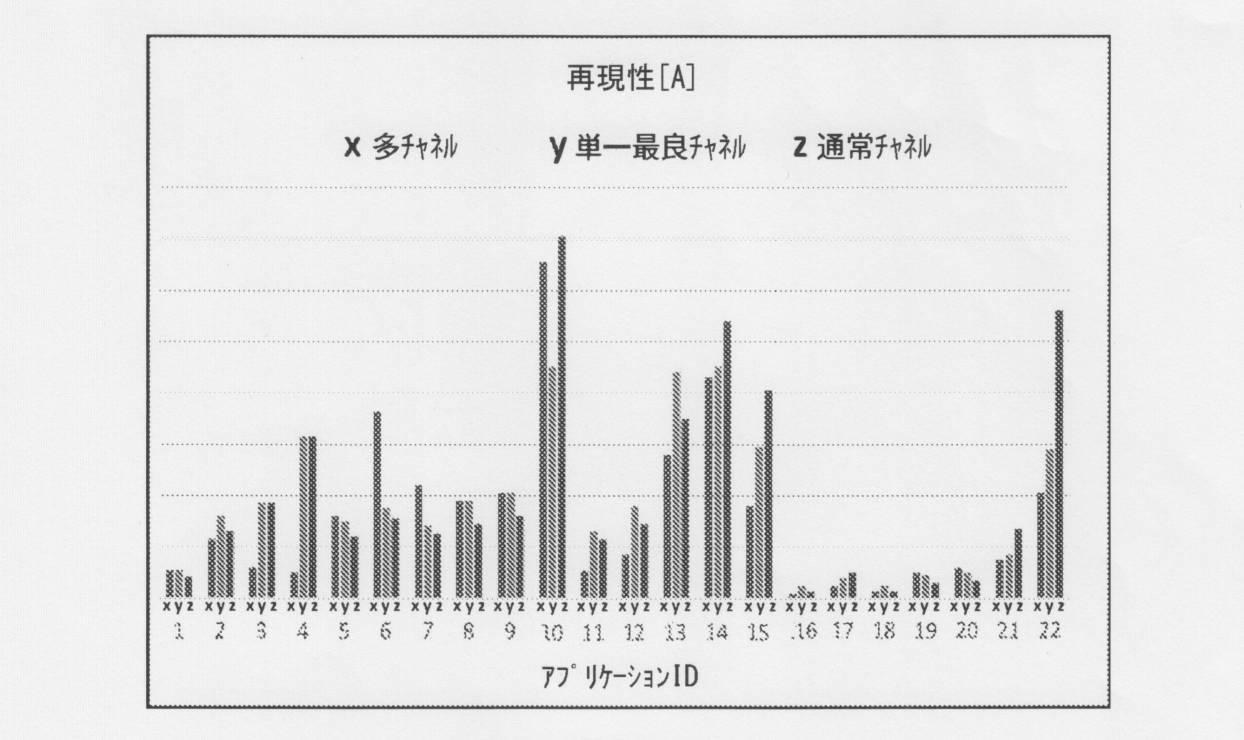
この発明の一実施態様では,計測スループット(metrology throughput)(TPT)は,多くの測定チャネルを含む計測レシピから開始し,通常の物理モデリングを使用して参照値を取得し,TPTが優れている少数のチャネル(たとえば2つの通常チャネルのみ)であって,そのうちの一つが精度とスループットのバランスが取れたソリューションを「転送」できるものを検索することによって最適化することができる。この効果が図3Aおよび図3Bに示されており,図3Aおよび図3Bは7つのレイヤ(層)にわたる22個の制御要素およびレイヤごとの複数のパラメータの調査を示す,この発明の実験結果を表している。図3Aおよび図3Bにおいて,参照値はCDSEMやTEMといった,物理モデリングまたは外部参照ツールのいずれかで提供されたものである。図3Aおよび図3Bに示すように,精度(図3A)および再現性(図3B)に重大なペナルティをもたらすことなく,多くのチャネルを単一のチャネルに転送(transfer)することができる。これによりTPTを3倍から4倍に増やすことができる。
Optimizing Throughput by Reducing the Number of Channels Measured In one embodiment of the invention, measurement throughput (TPT) begins with a measurement recipe that includes many measurement channels and uses conventional physical modeling. To get a reference value and search for a small number of channels with good TPT (eg only two regular channels), one of which can "forward" a solution with a balance of accuracy and throughput. It can be optimized by doing so. This effect is shown in FIGS. 3A and 3B, where FIGS. 3A and 3B show the experimental results of the present invention showing the investigation of 22 control elements across 7 layers and multiple parameters per layer. Represents. In FIGS. 3A and 3B, the reference values are provided by either physical modeling or external reference tools such as CDSEM and TEM. As shown in FIGS. 3A and 3B, many channels can be transferred to a single channel without incurring significant penalties for accuracy (FIG. 3A) and reproducibility (FIG. 3B). This allows the TPT to be increased 3 to 4 times.
この発明のこの実施形態によれば,トレーニング・ユニット114が,ユーザ定義されたまたは他の方法で所定所望のスループットを有するように制約された最適チャネルを自動的に選択する。
According to this embodiment of the invention, the
限られた量の参照データを処理する方法(Methods of handling a limited amount of reference data)
直接処理制御
この発明の一実施態様では,半導体製造において使用されるアドバンスト・プロセス・コントロール(Advanced Process Control)(APC)システムにおいて使用されるようなツール・ノブ制御ソリューション(tool knob control solutions)が,2つのレベルの変動ソース,すなわち処理ウェーハ内(バッチ)およびウェーハ間変動(バッチ間)に提供される。処理ツール(たとえばCMP時間またはエッチング温度を制御するノブ上のDOE)のレシピ・パラメータの範囲において測定される信号Sのセットを最初に取得することによって処理パラメータを直接制御するためにMLを使用することができる。次に予測モデル116は,ツール・ノブへのOCD信号を学習および較正するようにトレーニングされる。次に,予測モデル116を使用してツール・ノブへのフィードバックとして使用できる有効なノブ設定を予測することができる。
Methods of handling a limited amount of reference data
Direct Process Control In one embodiment of the invention, tool knob control solutions, such as those used in Advanced Process Control (APC) systems used in semiconductor manufacturing, are: Two levels of variation sources are provided: intra-processed wafer (batch) and inter-wafer variation (batch-to-batch). ML is used to directly control the processing parameters by first obtaining a set of signals S measured in the range of recipe parameters of the processing tool (eg DOE on the knob controlling the CMP time or etching temperature). be able to. The
2つの異なるDOEレベルを有する2つのグループの信号が与えられると,DOEレベルを基準として,トレーニング・ユニット114は,MLを使用してノブの変化に対するスペクトル応答,すなわちノブに対するスペクトル感度を抽出する。トレーニング・ユニット114はグループ間のスペクトル差を追跡し,グループのノミナル(公称値,nominal)は,好ましくは,ノブ効果が支配的なものになるように可能な限り近いものである。次に,学習した関係にしたがって将来の処理が調整され,パラメータの所望の目標結果を達成したり,処理およびツールのドリフトを調整して潜在的な障害を防止したりすることができる。この効果が図4Aおよび図4Bに示されており,これらは研磨時間(図4A)および意図された残りの厚さ(図4B)においてDOEがIMスペクトルを使用する予測モデル116によってどのように学習されたかを示すこの発明の実験結果を表している。図4Aおよび図4Bは,上記DOEのウェーハ・レベルの均一性にかかわらず,「有効ノブ」がWIW変動をキャプチャする(すなわち,上記モデルが各ウェーハの有効ノブ設定の範囲を予測する)ことを示している。この効果的なノブ技術が有用であることを確認するために,イスラエル国,レホヴォトのノバ メジャリング インスツルメント リミテッドからから市販されているNOVA T600(登録商標)MMSR Advanced Optical CD Metrologyツールを使用した物理アルゴリズムによって測定されたターゲットの残りの厚さの外部正解(external ground truth)に対して提示されている。このようなモデルは,WIWノブを備えた処理ツールへのフィードバックに使用することができる。図4Aに示すように,予測された有効研磨時間(「有効ノブ」)は、正解の研磨層厚と高い相関関係があり,他方で図2Bは基準(参照)に対する予測研磨厚効果を示している。
Given two groups of signals with two different DOE levels, the
データ拡張(Data augmentation)
シンプルなMLアルゴリズムには,説明しようとしている基礎となる物理学に関する事前知識が含まれていない。これは,それらの成功がデータの可用性(availability),より具体的には参照データの可用性に基づいていることを意味する。この発明の一実施形態では,予測モデル116をトレーニングするために使用されるトレーニング・データ・セットのサイズは,データの非常に複雑な確率分布を記述する能力を有するML方法のクラスである生成モデルによって(by means of generative models, which are a class of ML methods that have the ability of describing a highly complex probability distribution of data)増加する。単純な物理的アナロジーは統計物理学におけるボルツマン重み(Boltzmann weight)またはユークリッド量子論の経路積分形式(path integral formalism for Euclidean quantum theories)である。いずれの場合も,システムの自由度の振る舞い(たとえば統計物理学におけるスピンや量子電気力学における電子)を表す確率関数が定義される。これらの確率関数は明示的な形式を有しており,包含される物理学の実現を生成するために(to generate realizations of the physics involved)使用することができる。事実として,物理学の多くの分野では,このような形式は,物質の物理的特性を計算するための大規模なマルコフ連鎖モンテカルロ・シミュレーション(large scale Markov chain Monte-Carlo simulations)において使用される。データ・サイエンスの生成モデルは明示的または暗黙的であることがあり,明示的モデルでは確率関数が明示的に記述され(ボルツマン重みと同じ),暗黙的モデルではアルゴリズムが経験的データセットの統計を「学習」し,その後に同じ統計を用いて新しいデータ例を生成することができる。暗黙的方法の例には,変分オートエンコーダ(Variational Auto Encoders)や生成的敵対的ネットワーク(Generative Adversarial Networks)が含まれる。この発明の一実施態様では,これらの方法は,参照データセットを増加および多様化のために使用され,それによってトレーニング・ユニット114の性能が最適化され,基礎となる物理学を予測モデル116に反映する機械学習モデルの様々な特徴間の事前情報および制約の導入が可能になる。
Data augmentation
The simple ML algorithm does not contain any prior knowledge of the underlying physics to be explained. This means that their success is based on the availability of data, and more specifically the availability of reference data. In one embodiment of the invention, the size of the training data set used to train the
処理堅牢性の解決(Solving process robustness)
処理堅牢性を解決するために,この発明の一実施態様では,MLアルゴリズムとビッグデータ・システムの組み合わせが採用され,これは以下のようにレシピを作成し,これを監視かつ制御する。
Solving process robustness
In order to solve the processing robustness, one embodiment of the present invention employs a combination of an ML algorithm and a big data system, which creates a recipe and monitors and controls it as follows.
・レシピ・トレーニング:
MLを使用して可能な限り自動的に,数百のスペクトル・タイプ(「測定レシピ」)にわたることがあるビッグ・データ・データベース内において,数か月,場合によっては数年にわたってユーザがトレーニング・データをクエリできるようにする。
・ Recipe training:
Users are trained for months and even years in big data databases, which can span hundreds of spectral types (“measurement recipes”) as automatically as possible using ML. Allow data to be queried.
・レシピの検証:
相互検証とブラインド・テスト方法論を使用して,レシピの品質に関するカスタマー・フィードバックを生成する。
・ Recipe verification:
Use cross-validation and blind testing methodologies to generate customer feedback on recipe quality.
・レシピ監視:
トレーニング・データを用いて,監視防御インデックス(monitor defense indices)を,これらのインデックスの仕様とともに生成する。次に,これらのインデックスをインラインで監視し,たとえばSEMI標準SPCルール(SEMI standard SPC rules)を採用等することでレシピの精度が低下した場合にフラグを立てる。
・ Recipe monitoring:
The training data is used to generate monitor defense indices along with the specifications of these indexes. Next, these indexes are monitored inline, and a flag is set when the accuracy of the recipe is lowered by, for example, adopting the SEMI standard SPC rules.
・レシピ更新:
監視(モニタ)が修復のために計測レシピにフラグを立てると,自動再トレーニング・シーケンスが開始され,新しいレシピがその検証結果とともに自動的に提案される。
・ Recipe update:
When the monitor flags the measurement recipe for repair, an automatic retraining sequence is started and a new recipe is automatically proposed with the validation result.
図5Aに示すこの実施態様は,外側円が参照ツールを表しており,これはNOVA T600(登録商標)-MMSRのようなハイエンドの,チャネルが豊富な光学計測ツール,またはXPS,SEMまたはTEMなどの非光学参照(non-optical reference)とすることができる。通常,これらのツールのCOOは高く,TPTは低く,破壊性,ツール・マッチング,再現性などの重要な生産性の課題も反映する。精度的には,これらのツールは情報量が多いという特徴がある(たとえば高解像度のイメージング・ツールやマルチチャネルの光学ツール)。内側円は,イスラエル,レホヴォトのノバ メジャリング インスツルメント リミテッドからから市販されているNOVA i550(登録商標)法線入射チャネル統合計測(normal incidence channel integrated metrology)(IM)ツールのような,高速かつコンパクトなOCDツールを表しており,これは,スループットが高く,必要なサンプリングレート(ダイの数)ですべてのウェーハをインラインで測定する機能があり,入力がSinner-circleで,Preferenceについての予測を出力するインラインで実行されるMLアルゴリズムを備えるものである。 In this embodiment shown in FIG. 5A, the outer circle represents a reference tool, such as a high-end, channel-rich optical measurement tool such as NOVA T600®-MMSR, or XPS, SEM or TEM. Can be a non-optical reference. These tools typically have high COOs, low TPTs, and reflect important productivity challenges such as destructiveness, tool matching, and reproducibility. To be precise, these tools are characterized by a large amount of information (for example, high resolution imaging tools and multi-channel optical tools). The inner circle is fast and fast, like the NOVA i550® normal incidence channel integrated metrology (IM) tool commercially available from Nova Measuring Instrument Limited in Rehovot, Israel. Represents a compact OCD tool, which has high throughput, has the ability to measure all wafers in-line at the required sampling rate (number of dies), has a Sinner-circle input, and makes predictions about Preferences. It includes an ML algorithm that is executed inline to output.
システム・アーキテクチャ(System architecture)
図5Bは,この明細書に記載のこの発明の一または複数の実施形態を実装するためのアーキテクチャを示しており,コンピュータ・クラスタが,ウェブサーバレイヤ(たとえばNodeJS(商標))およびビッグデータレイヤ(たとえば,メリーランド州,フォレストヒルのアパッチ・ソフトウエア・ファウンデーション(Apache Software Foundation)から市販されているHadoop(商標)クラスタ)を含む。ビッグデータレイヤは,スケーラブルかつ分散された方法においてデータを保存および処理するために用いられる。ウェブサーバレイヤは,ユーザが制御システムにおける処理ジョブを規定し,制御システムのレポートおよび実行ステータスを表示できるようにする。両レイヤはスケーラビリティ,高可用性および負荷分散を実現するためにマイクロサービス・アプローチ(micro-services approach)を使用して設計される。メッセージ・キューが用いられてサービス間の通信が行われ,密結合(tight coupling)が減らされる。ビッグデータレイヤのパフォーマンスを向上させるために,さまざまなデータ前処理パイプラインが採用される。
System architecture
FIG. 5B shows an architecture for implementing one or more embodiments of the invention described herein in which a computer cluster can be a web server layer (eg, NodeJS ™) and a big data layer (eg, NodeJS ™). For example, Hadoop ™ clusters marketed by the Apache Software Foundation in Foresthill, Maryland. Big data layers are used to store and process data in a scalable and distributed manner. The web server layer allows users to define processing jobs in the control system and display control system reports and execution status. Both layers are designed using a micro-services approach for scalability, high availability and load balancing. Message queues are used to communicate between services and reduce tight coupling. Various data preprocessing pipelines are adopted to improve the performance of big data layers.
データサイズおよび長期処理の堅牢性(Data size and long-term process robustness)
ビッグデータ・システムを使用すると,予測モデル116のトレーニングに利用可能なトレーニング・データの量を増やすことができ,予測モデル116をリアルタイムで改善および更新でき,これによりデータ管理のオーバーヘッドによる精度制限がなくなり,長期的な処理の堅牢性が確保される。図6Aおよび図6Bは,FEOLレイヤに適用された予測モデル116の改善された精度性能の2つの例を示している。ここで参照(基準)は,NOVA T600(登録商標)−MMSRで開発された物理モデルとし,予測モデル116には推論のために2つの通常チャネルを使用した。プロットは,〜2000ダイにわたるブラインド・テスト結果の1σとして定義される予測モデル116の精度が,モデルのトレーニングに使用されるウェーハ(各ウェーハは〜15ダイを持つ)の数にどのように依存するか示している。図6Aに示すように,トレーニング・サイズ(train size)を5ウェーハから200ウェーハに増やすと精度を45%向上させることができる(13A→6A)。このような大きなサンプルで飽和することは一般的ではなく,DOEが存在する場合,現場では数十倍の良好な結果が得られることがよくある(we often see good results on tens on sites provided a DOE is present)。図6Bは別の状況を示すもので,ここでは,予測モデル116の精度が,使用されるデータの量だけではなく,これをトレーニングするために使用されるデータに強く依存していることを示している。具体的には,図6bは,ブラインド・テスト・ウェーハに時間的に最も近い(closest in time)〜20枚のウェーハでトレーニングした場合(曲線600で示す),モデルが,ブラインド・テストから最も遠い100枚のウェーハでトレーニングした場合(曲線602で示す)と同じレベルの精度に収束したことを示している。これらの曲線の間にはベンチマーク曲線(曲線604で示す)があり,これは時間の重要性の記憶を「失う」ためのデータのランダムなシャッフル(a random shuffle of the data so as to ‘lose’ memory of the important of time)を記述する。これは,ウェーハのタイプが重要であり,このアプリケーションが,この実施形態のビッグデータ・システムが可能であるMLレシピの動的更新から利益を得るであろうことを示している。
Data size and long-term process robustness
Big data systems allow you to increase the amount of training data available for training
上記のレシピ更新ステップは,再トレーニングの実行に使用されるデータの選択と同様に自動的に実行される。この選択では,利用可能なすべてのデータを使用するようにしてもよく,または各ウェーハの監視フラグの値および/または処理されている他のウェーハへの所与のウェーハの時間的または処理空間的な近接性を考慮する論理に基づくことができる。たとえば,再トレーニングに利用可能なデータにおいてウェーハごとに異なる重みpを設定することができる。上記重みpは,そのウェーハのフラグ値,スペクトル自体,および/またはウェーハやロットIDなどの他のメタデータ特性に依存させてもよい。これが図7に示されている。 The above recipe update step is performed automatically, similar to the selection of data used to perform the retraining. In this selection, all available data may be used, or the value of the monitoring flag for each wafer and / or the temporal or processing spatial of a given wafer to other wafers being processed. Can be based on logic that considers close proximity. For example, different weights p can be set for each wafer in the data available for retraining. The weight p may depend on the flag value of the wafer, the spectrum itself, and / or other metadata characteristics such as the wafer or lot ID. This is shown in FIG.
この明細書に記載のこの発明の任意の態様は,従来の技術にしたがって,非一時的なコンピュータ読み取り可能な媒体に具現化されるコンピュータ・ハードウェアおよび/またはコンピュータ・ソフトウェア,一または複数のコンピュータ・プロセッサを含むコンピュータ・ハードウェア,コンピュータ・メモリ,I/Oデバイス,および従来の手法にしたがって相互運用するネットワーク・インターフェースに実装することができる。 Any aspect of the invention described herein is computer hardware and / or computer software, one or more computers, embodied in non-temporary computer-readable media according to prior art. It can be implemented in computer hardware including processors, computer memory, I / O devices, and network interfaces that interoperate according to conventional methods.
この明細書において使用される「プロセッサ」または「デバイス」という用語は,たとえばCPU(中央処理装置)および/または他の処理回路を含むものなどの任意の処理デバイスを含むことを意図していることを理解されたい。「プロセッサ」または「デバイス」という用語は,複数の処理デバイスを指す場合があり,処理デバイスに関連する様々な要素が他の処理デバイスによって共有される場合があることも理解されたい。 As used herein, the term "processor" or "device" is intended to include any processing device, such as those containing a CPU (Central Processing Unit) and / or other processing circuits. Please understand. It should also be understood that the term "processor" or "device" may refer to multiple processing devices, and various elements associated with the processing device may be shared by other processing devices.
この明細書において使用される「メモリ」という用語は,処理装置またはCPUと協調するメモリ,たとえば,RAM,ROM,固定メモリ装置(たとえばハードドライブ),リムーバブル・メモリ装置(たとえばディスク),フラッシュ・メモリ等を含むことを意図する。このようなメモリをコンピュータ読み取り可能な記憶媒体と考えてもよい。 As used herein, the term "memory" refers to memory that works with a processor or CPU, such as RAM, ROM, fixed memory devices (eg hard drives), removable memory devices (eg disks), flash memory. Etc. are intended to be included. Such a memory may be considered as a computer-readable storage medium.
さらには,この明細書において使用される「入力/出力装置」または「I/O装置」という用語は,たとえば処理ユニットにデータを入力するための一または複数の入力装置(たとえばキーボード,マウス,スキャナ等),および/または処理ユニットと協調して結果を提示する一または複数の出力装置(たとえばスピーカ,ディスプレイ,プリンタ等)を含むことを意図する。 Furthermore, the term "input / output device" or "I / O device" as used herein refers to, for example, one or more input devices (eg, keyboard, mouse, scanner) for inputting data into a processing unit. Etc.), and / or intended to include one or more output devices (eg, speakers, displays, printers, etc.) that present results in concert with the processing unit.
この発明の実施形態は,システム,方法,および/またはコンピュータプログラム製品を含む。コンピュータプログラム製品は,プロセッサにこの発明の態様を実行させるためのコンピュータ読み取り可能なプログラム命令を有するコンピュータ読み取り可能な記憶媒体(または複数の媒体)を含む。 Embodiments of the present invention include systems, methods, and / or computer program products. Computer program products include a computer-readable storage medium (or multiple media) having computer-readable program instructions for causing a processor to perform aspects of the invention.
コンピュータ読み取り可能な記憶媒体は,命令実行デバイスによって使用される命令を保持および記憶することができる有形デバイスとすることができる。コンピュータ読み取り可能な記憶媒体は,たとえば,これらに限定されないが,電子記憶装置,磁気記憶装置,光記憶装置,電磁記憶装置,半導体記憶装置,またはこれらの任意の適切な組み合わせとすることができる。コンピュータ読み取り可能な記憶媒体のより具体的な例の非網羅的なリストには,可搬のコンピュータディスケット,ハードディスク,ランダムアクセスメモリ(RAM),読み取り専用メモリ(ROM),消去可能なプログラム可能な読み取り専用メモリ(EPROMまたはフラッシュ・メモリ),静的ランダムアクセスメモリ(SRAM)、可搬のコンパクトディスク読み取り専用メモリ(CD−ROM),デジタル多用途ディスク(DVD),メモリスティック,フロッピーディスク,パンチカードまたは指示が記録された溝内隆起構造のような機械的符号化装置,およびこれらの任意の適切な組み合わせを含む。この明細書で使用されるコンピュータ読み取り可能な記憶媒体は,電波または他の自由に伝播する電磁波,導波管または他の伝送媒体を通って伝播する電磁波(たとえば光ファイバケーブルを通過する光パルス)またはワイヤを介して送信される電気信号などの一時的信号自体と解釈されるべきではない。 The computer-readable storage medium can be a tangible device capable of holding and storing the instructions used by the instruction executing device. Computer-readable storage media can be, for example, but not limited to, electronic storage devices, magnetic storage devices, optical storage devices, electromagnetic storage devices, semiconductor storage devices, or any suitable combination thereof. A non-exhaustive list of more specific examples of computer-readable storage media includes portable computer disks, hard disks, random access memory (RAM), read-only memory (ROM), and erasable programmable reads. Dedicated memory (EPROM or flash memory), static random access memory (SRAM), portable compact disk read-only memory (CD-ROM), digital versatile disk (DVD), memory stick, floppy disk, punch card or Includes mechanical coding devices such as grooved ridge structures in which instructions are recorded, and any suitable combination thereof. The computer-readable storage medium used herein is radio waves or other freely propagating electromagnetic waves, electromagnetic waves propagating through waveguides or other transmission media (eg, optical pulses through optical fiber cables). Or it should not be interpreted as a temporary signal itself, such as an electrical signal transmitted over a wire.
この明細書に記載のコンピュータ読み取り可能なプログラム命令は,コンピュータ読み取り可能な記憶媒体からそれぞれのコンピューティング/処理デバイスに,またはネットワークたとえばインターネット,ローカルエリアネットワーク,ワイドエリアネットワークおよび/またはワイヤレスネットワークを介して外部コンピュータまたは外部記憶デバイスに,ダウンロードすることができる。ネットワークは,銅線伝送ケーブル,光ファイバー,無線伝送,ルーター,ファイアウォール,スイッチ,ゲートウェイコンピューターおよび/またはエッジサーバーを含むことができる。各コンピューティング/処理デバイスのネットワークアダプタカードまたはネットワーク・インターフェースは,ネットワークからコンピュータ読み取り可能なプログラム命令を受信し,それぞれのコンピューティング/処理デバイス内のコンピュータ読み取り可能な記憶媒体に記憶するためにコンピュータ読み取り可能なプログラム命令を転送する。 The computer-readable program instructions described herein are from computer-readable storage media to their respective computing / processing devices, or over networks such as the Internet, local area networks, wide area networks and / or wireless networks. It can be downloaded to an external computer or external storage device. Networks can include copper transmission cables, fiber optics, wireless transmissions, routers, firewalls, switches, gateway computers and / or edge servers. The network adapter card or network interface of each computing / processing device receives computer-readable program instructions from the network and computer-reads them for storage on a computer-readable storage medium within each computing / processing device. Transfer possible program instructions.
この発明の動作を実行するためのコンピュータ読み取り可能なプログラム命令は,アセンブラ命令,命令セットアーキテクチャ(ISA)命令,機械命令,機械依存命令,マイクロコード,ファームウェア命令,状態設定データ,もしくはソースコード,またはJava,Smalltalk,C ++などのオブジェクト指向プログラミング言語,「C」プログラミング言語または同様のプログラミング言語などの従来の手続き型プログラミング言語を含む,一つ以上のプログラミング言語の任意の組み合わせで記述されるオブジェクトコードのいずれかとすることができる。コンピュータ読み取り可能なプログラム命令は,完全にユーザのコンピュータ上で,一部はユーザのコンピュータ上でスタンドアロンソフトウェアパッケージとして,一部はユーザのコンピュータ上で一部はリモートコンピュータ上で,または完全にリモートコンピュータまたはサーバ上で,実行される。後者のシナリオでは,リモートコンピュータは,ローカルエリアネットワーク(LAN)またはワイドエリアネットワーク(WAN)を含む任意のタイプのネットワークを介してユーザのコンピュータに接続するか,外部コンピュータに接続することができる(たとえばインターネットサービスプロバイダを使用したインターネット経由)。いくつかの実施形態では,たとえばプログラマブルロジック回路,フィールドプログラマブルゲートアレイ(FPGA)またはプログラマブルロジックアレイ(PLA)を含む電子回路が,この発明の態様を実行するために,コンピュータ読み取り可能なプログラム命令の状態情報を利用して電子回路をパーソナライズすることにより,コンピュータ読み取り可能プログラム命令を実行することができる。 Computer-readable program instructions for performing the operations of the present invention are assembler instructions, instruction set architecture (ISA) instructions, machine instructions, machine-dependent instructions, microcodes, firmware instructions, state-setting data, or source code, or Objects described in any combination of one or more programming languages, including object-oriented programming languages such as Java, Smalltalk, and C ++, and traditional procedural programming languages such as the "C" programming language or similar programming languages. It can be any of the codes. Computer-readable program instructions are entirely on the user's computer, partly on the user's computer as a stand-alone software package, partly on the user's computer, partly on the remote computer, or completely on the remote computer. Or it is executed on the server. In the latter scenario, the remote computer can connect to the user's computer or to an external computer via any type of network, including local area networks (LANs) or wide area networks (WANs) (eg,). Via the Internet using an Internet service provider). In some embodiments, an electronic circuit, including, for example, a programmable logic circuit, a field programmable gate array (FPGA) or a programmable logic array (PLA), is a state of computer-readable program instructions for performing aspects of the invention. By using information to personalize electronic circuits, computer-readable program instructions can be executed.
この発明の態様は,この発明の実施形態による方法,装置(システム)およびコンピュータプログラム製品のフローチャートおよび/またはブロック図を参照してこの明細書に記載される。フローチャートおよび/またはブロック図の各ブロック,およびフローチャートおよび/またはブロック図のブロックの組み合わせはコンピュータ読み取り可能なプログラム命令によって実装できることが理解されよう。 Aspects of the invention are described herein with reference to flowcharts and / or block diagrams of methods, devices (systems) and computer program products according to embodiments of the invention. It will be appreciated that each block of the flowchart and / or block diagram, and the combination of blocks of the flowchart and / or block diagram, can be implemented by computer-readable program instructions.
これらのコンピュータ読み取り可能なプログラム命令は,汎用コンピュータ,専用コンピュータ,またはその他のプログラム可能なデータ処理装置のプロセッサに提供され,コンピュータのプロセッサまたは他のプログラム可能なデータ処理装置を介して命令を実行する機械が製造され,フローチャートおよび/または一または複数のブロックにおいて特定される機能/作用を実施するための手段を作成することができる。これらのコンピュータ読み取り可能なプログラム命令はまた,コンピュータ読み取り可能な記憶媒体に記憶することができ,コンピュータ,プログラム可能なデータ処理装置および/または他のデバイスに特定の態様において機能するように指示することができる。コンピュータ読み取り可能な記憶媒体はそこに記憶されたフローチャートおよび/または一または複数のブロックにおいて特定される機能/作用の態様を実装する命令を含む製造品を含む。 These computer-readable program instructions are provided to the processor of a general-purpose computer, a dedicated computer, or other programmable data processing device, and execute the instructions through the computer's processor or other programmable data processing device. A machine can be manufactured to create means for performing a flowchart and / or a function / action identified in one or more blocks. These computer-readable program instructions can also be stored on a computer-readable storage medium and instruct the computer, programmable data processing device and / or other device to function in a particular manner. Can be done. Computer-readable storage media include manufactured goods containing flowcharts stored therein and / or instructions that implement modes of function / action identified in one or more blocks.
コンピュータ読み取り可能なプログラム命令はまた,コンピュータ,他のプログラム可能なデータ処理装置,または他のデバイスにロードされ,コンピュータ上,他のプログラム可能な装置上または他のデバイス上で一連の操作ステップを実行させ,コンピュータ実装処理を生成することができる。コンピュータ,他のプログラム可能な装置または他のデバイス上で実行される命令は,フローチャートおよび/または一または複数のブロック図において特定される機能/作用を実施する。 Computer-readable program instructions are also loaded onto a computer, other programmable data processor, or other device to perform a series of operational steps on a computer, another programmable device, or another device. It can be made to generate a computer implementation process. Instructions executed on a computer, other programmable device, or other device perform the functions / actions identified in the flow chart and / or one or more block diagrams.
図面中のフローチャートおよびブロック図は,この発明の様々な実施形態によるシステム,方法,およびコンピュータプログラム製品に実装可能なアーキテクチャ,機能および動作を示している。これに関して,フローチャートまたはブロック図の各ブロックは,コンピュータ命令のモジュール,セグメントまたは部分を表すことができ,これは特定の論理機能を実装するための一または複数の実行可能なコンピュータ命令を含む。いくつかの他の実装形態では,ブロックに示されている機能は,図面中に示されている順序から外れて動作することがある。たとえば,連続して示される2つのブロックは,実際には実質的に同時に実行されたり,または関連する機能に応じてブロックが逆の順序で実行されたりする場合もある。フローチャートおよびブロック図の各ブロックならびにブロックの組み合わせは,特定の機能または動作を実行する専用ハードウェアベースおよび/またはソフトウェアベースのシステムによって実装できることにも留意されたい。 Flow charts and block diagrams in the drawings show the architectures, functions, and operations that can be implemented in systems, methods, and computer program products according to various embodiments of the present invention. In this regard, each block in a flowchart or block diagram can represent a module, segment or portion of a computer instruction, which contains one or more executable computer instructions to implement a particular logical function. In some other implementations, the functions shown in the blocks may operate out of the order shown in the drawing. For example, two blocks shown in succession may actually be executed at substantially the same time, or the blocks may be executed in reverse order depending on the related function. It should also be noted that each block in the flow chart and block diagram and the combination of blocks can be implemented by a dedicated hardware-based and / or software-based system that performs a particular function or operation.
この発明の様々な実施形態の説明は,例示目的で提示されており,網羅的であることを意図するものではなく,開示する実施形態に限定されることを意図するものではない。たとえば,本書に記載のシステムおよび方法は,半導体ウェーハ上の任意の構造に適用可能である。説明する実施形態の範囲および精神から逸脱することのない多くの修正および変形が当業者には明らかであろう。 The description of the various embodiments of the present invention is presented for illustrative purposes only and is not intended to be exhaustive and is not intended to be limited to the disclosed embodiments. For example, the systems and methods described herein are applicable to any structure on a semiconductor wafer. Many modifications and variations that do not deviate from the scope and spirit of the embodiments described will be apparent to those of skill in the art.
Claims (16)
参照計測ツールを使用しかつ第2の測定プロトコルにしたがって,上記第1セットの半導体ウェーハ・ターゲットの所定パラメータの値を収集し,
スペクトル変動性の一または複数の所定ソースのそれぞれについて,上記スペクトル取得ツールを使用しかつ上記第1の測定プロトコルにしたがって,上記第1セットの半導体ウェーハ・ターゲットに対応する第2セットの半導体ウェーハ・ターゲット上のスペクトルの変動セットを収集し,ここで上記スペクトルの変動セットはスペクトル変動性を具体化するものであり,
収集されたスペクトルのセットおよびパラメータ値を使用して,機械学習を用いて予測モデルをトレーニングし,かつ上記予測モデルに関連する損失関数を最小化し,
ここで上記予測モデルは,第3セットの半導体ウェーハ・ターゲットの製造スペクトルを使用して所定パラメータのいずれかの値を予測するために使用されるように構成され,上記製造スペクトルは上記スペクトル取得ツールを使用しかつ上記第1の測定プロトコルにしたがって収集され,
上記損失関数は,上記スペクトル変動性の一または複数の所定ソースのそれぞれについて上記スペクトル変動性を表す項を組み込むことによって最小化される,
半導体計測方法。 Collect a baseline set of spectra on the first set of semiconductor wafer targets using a spectrum acquisition tool and according to the first measurement protocol.
Using the reference measurement tool and according to the second measurement protocol, the values of the predetermined parameters of the above first set of semiconductor wafer targets are collected.
For each of one or more predetermined sources of spectral variability, a second set of semiconductor wafers corresponding to the first set of semiconductor wafer targets using the spectrum acquisition tool and according to the first measurement protocol. A set of spectral variability on the target is collected, where the above spectral variability set embodies spectral variability.
Using the set of spectra and parameter values collected, we trained the predictive model using machine learning and minimized the loss function associated with the predictive model.
Here, the prediction model is configured to be used to predict the value of any of the predetermined parameters using the production spectrum of the third set of semiconductor wafer targets, where the production spectrum is the spectrum acquisition tool. And collected according to the first measurement protocol above,
The loss function is minimized by incorporating a term representing the spectral variability for each of the one or more predetermined sources of the spectral variability.
Semiconductor measurement method.
予測モデルを使用して上記製造散乱測定スペクトルに基づいて所定パラメータのいずれかの予測値を生成することをさらに含む,
請求項1に記載の方法。 Collecting manufacturing scattering measurement spectra during manufacturing of manufacturing semiconductor wafers
It further comprises using a predictive model to generate a predictive value of any of the predetermined parameters based on the manufacturing scattering measurement spectrum described above.
The method according to claim 1.
スペクトル変動性の一または複数の所定ソースのそれぞれについて,上記第1の測定プロトコルにしたがって,上記第1セットの半導体ウェーハ・ターゲットに対応する第2セットの半導体ウェーハ・ターゲット上の,上記スペクトル変動性を具体化する散乱測定スペクトルの変動セットを収集するように構成される,スペクトル取得ツールと,
第2の測定プロトコルにしたがって,上記第1セットの半導体ウェーハ・ターゲットの所定パラメータの値を収集する参照計測ツールと,
収集されたスペクトルのセットおよびパラメータ値を使用して,機械学習を用いて予測モデルをトレーニングし,かつ予測モデルに関連する損失関数を最小化するように構成されるトレーニング・ユニットと,を備え,
上記予測モデルが第3セットの半導体ウェーハ・ターゲットの製造スペクトルを用いて所定パラメータのいずれかの値を予測するために使用されるように構成され,上記製造スペクトルが上記スペクトル取得ツールを使用して上記第1の測定プロトコルにしたがって収集され,
上記損失関数が,スペクトル変動性の一または複数の所定のソースのそれぞれについて,上記スペクトル変動性を表す項を組み込むことによって最小化される,
半導体計測システム。 A baseline set of scattering measurement spectra on the first set of semiconductor wafer targets is collected according to the first measurement protocol.
For each of one or more predetermined sources of spectral variability, the spectral variability on a second set of semiconductor wafer targets corresponding to the first set of semiconductor wafer targets according to the first measurement protocol. A spectrum acquisition tool and a spectrum acquisition tool configured to collect a variation set of scattering measurement spectra that embodies.
A reference measurement tool that collects the values of the given parameters of the first set of semiconductor wafer targets according to the second measurement protocol.
With a training unit configured to train the predictive model using machine learning using the collected spectral set and parameter values, and to minimize the loss function associated with the predictive model.
The prediction model is configured to be used to predict the value of any of a given parameter using the production spectrum of a third set of semiconductor wafer targets, and the production spectrum is configured using the spectrum acquisition tool. Collected according to the first measurement protocol above
The loss function is minimized by incorporating a term representing the spectral variability for each of one or more predetermined sources of spectral variability.
Semiconductor measurement system.
上記予測モデルを使用して上記製造散乱計測スペクトルに基づいて上記所定パラメータのいずれかの予測値を生成するように構成される予測ユニットをさらに備えている,
請求項9に記載のシステム。 The spectrum acquisition tool is configured to collect the manufacturing scattering measurement spectrum during the manufacturing of the manufacturing semiconductor wafer.
It further comprises a prediction unit configured to generate a prediction value of any of the above predetermined parameters based on the manufacturing scattering measurement spectrum using the prediction model.
The system according to claim 9.
15. A processing control unit further comprising a processing control unit configured to provide input to a semiconductor manufacturing tool based on the predicted values to control the operation of the semiconductor manufacturing tool during manufacturing of the manufactured semiconductor wafer. The system described in.
Priority Applications (1)
| Application Number | Priority Date | Filing Date | Title |
|---|---|---|---|
| JP2021179992A JP7218412B2 (en) | 2018-06-14 | 2021-11-04 | Semiconductor manufacturing metrology and process control |
Applications Claiming Priority (3)
| Application Number | Priority Date | Filing Date | Title |
|---|---|---|---|
| US201862684817P | 2018-06-14 | 2018-06-14 | |
| US62/684,817 | 2018-06-14 | ||
| PCT/IB2019/054994 WO2019239380A1 (en) | 2018-06-14 | 2019-06-14 | Metrology and process control for semiconductor manufacturing |
Related Child Applications (1)
| Application Number | Title | Priority Date | Filing Date |
|---|---|---|---|
| JP2021179992A Division JP7218412B2 (en) | 2018-06-14 | 2021-11-04 | Semiconductor manufacturing metrology and process control |
Publications (2)
| Publication Number | Publication Date |
|---|---|
| JP2021521654A JP2021521654A (en) | 2021-08-26 |
| JP6974635B2 true JP6974635B2 (en) | 2021-12-01 |
Family
ID=68843046
Family Applications (3)
| Application Number | Title | Priority Date | Filing Date |
|---|---|---|---|
| JP2020569886A Active JP6974635B2 (en) | 2018-06-14 | 2019-06-14 | Semiconductor manufacturing measurement and processing control |
| JP2021179992A Active JP7218412B2 (en) | 2018-06-14 | 2021-11-04 | Semiconductor manufacturing metrology and process control |
| JP2023009145A Active JP7629945B2 (en) | 2018-06-14 | 2023-01-25 | Semiconductor Manufacturing Metrology and Process Control |
Family Applications After (2)
| Application Number | Title | Priority Date | Filing Date |
|---|---|---|---|
| JP2021179992A Active JP7218412B2 (en) | 2018-06-14 | 2021-11-04 | Semiconductor manufacturing metrology and process control |
| JP2023009145A Active JP7629945B2 (en) | 2018-06-14 | 2023-01-25 | Semiconductor Manufacturing Metrology and Process Control |
Country Status (7)
| Country | Link |
|---|---|
| US (4) | US11093840B2 (en) |
| JP (3) | JP6974635B2 (en) |
| KR (3) | KR102349299B1 (en) |
| CN (2) | CN114997408A (en) |
| IL (1) | IL279273B (en) |
| TW (4) | TWI883718B (en) |
| WO (1) | WO2019239380A1 (en) |
Families Citing this family (32)
| Publication number | Priority date | Publication date | Assignee | Title |
|---|---|---|---|---|
| US11940488B2 (en) | 2017-01-05 | 2024-03-26 | Xcalipr Corporation | Systems and methods for high precision optical characterization of carrier transport properties in semiconductor manufacturing |
| US11093840B2 (en) * | 2018-06-14 | 2021-08-17 | Nova Measuring Instruments Ltd. | Metrology and process control for semiconductor manufacturing |
| KR20220083811A (en) * | 2019-10-23 | 2022-06-20 | 램 리써치 코포레이션 | Determination of recipes for semiconductor fabrication |
| CN114930117B (en) * | 2020-01-06 | 2026-01-20 | 诺威有限公司 | Combining physical modeling and machine learning |
| US11256967B2 (en) | 2020-01-27 | 2022-02-22 | Kla Corporation | Characterization system and method with guided defect discovery |
| CN117892689A (en) * | 2020-04-06 | 2024-04-16 | 诺威有限公司 | System, method and storage medium for semiconductor manufacturing |
| KR102801221B1 (en) * | 2020-04-29 | 2025-04-30 | 삼성전자주식회사 | Inspection apparatus of wafer and method |
| US11209737B1 (en) | 2020-06-30 | 2021-12-28 | Kla Corporation | Performance optimized scanning sequence for eBeam metrology and inspection |
| US11688616B2 (en) | 2020-07-22 | 2023-06-27 | Applied Materials, Inc. | Integrated substrate measurement system to improve manufacturing process performance |
| US12283503B2 (en) | 2020-07-22 | 2025-04-22 | Applied Materials, Inc. | Substrate measurement subsystem |
| WO2022028805A1 (en) * | 2020-08-06 | 2022-02-10 | Asml Netherlands B.V. | Method and apparatus for concept drift mitigation |
| US20220066411A1 (en) * | 2020-08-31 | 2022-03-03 | Applied Materials, Inc. | Detecting and correcting substrate process drift using machine learning |
| KR20230070211A (en) * | 2020-09-18 | 2023-05-22 | 바스프 에스이 | chemical production |
| CN115280468B (en) * | 2021-03-01 | 2025-10-14 | 株式会社日立高新技术 | Experimental key point recommendation device, experimental key point recommendation method and semiconductor device manufacturing system |
| WO2022233546A1 (en) * | 2021-05-06 | 2022-11-10 | Asml Netherlands B.V. | Method for determining a stochastic metric relating to a lithographic process |
| KR20230052450A (en) | 2021-10-13 | 2023-04-20 | 삼성전자주식회사 | Method of predicting characteristic of semiconductor device and computing device performing the same |
| US20230128610A1 (en) * | 2021-10-25 | 2023-04-27 | Kla Corporation | Continuous Machine Learning Model Training for Semiconductor Manufacturing |
| CN114357940B (en) * | 2022-01-10 | 2026-04-24 | 长鑫存储技术有限公司 | Semiconductor structure analysis methods, analysis systems, media and electronic devices |
| KR102504761B1 (en) * | 2022-01-25 | 2023-02-28 | (주)오로스 테크놀로지 | Method for Measuring Properties of Thin Film |
| US12181271B2 (en) * | 2022-02-17 | 2024-12-31 | Kla Corporation | Estimating in-die overlay with tool induced shift correction |
| US20250123571A1 (en) * | 2022-04-07 | 2025-04-17 | Nova Ltd. | Full-wafer metrology up-sampling |
| US20240037442A1 (en) * | 2022-07-26 | 2024-02-01 | Applied Materials, Inc. | Generating indications of learning of models for semiconductor processing |
| EP4602437A1 (en) * | 2022-10-14 | 2025-08-20 | Applied Materials, Inc. | Determining substrate profile properties using machine learning |
| IL321482A (en) * | 2022-12-29 | 2025-08-01 | Nova Ltd | High throughput optical measurement system |
| CN120712526A (en) * | 2023-02-22 | 2025-09-26 | Asml荷兰有限公司 | Method and system for selecting patterns based on similarity indicators |
| CN116339145B (en) * | 2023-03-24 | 2025-09-05 | 长鑫存储技术有限公司 | Machine parameter control method, equipment and storage medium |
| US12587274B2 (en) | 2023-03-28 | 2026-03-24 | Quantum Generative Materials Llc | Satellite optimization management system based on natural language input and artificial intelligence |
| WO2024238401A2 (en) * | 2023-05-12 | 2024-11-21 | Tignis, Inc. | Optimizing semiconductor manufacturing processes using machine learning |
| CN118296366B (en) * | 2023-11-14 | 2025-03-14 | 张江国家实验室 | Training method for multi-solution problem in machine learning, X-ray measurement method and device |
| US12603701B2 (en) | 2023-12-27 | 2026-04-14 | Quantum Generative Materials Llc | Distributed satellite constellation management and control system |
| US12368503B2 (en) | 2023-12-27 | 2025-07-22 | Quantum Generative Materials Llc | Intent-based satellite transmit management based on preexisting historical location and machine learning |
| CN119987320B (en) * | 2025-04-02 | 2025-06-24 | 浙江求是半导体设备有限公司 | Control method and device for automatically adjusting thinning thickness of wafer |
Family Cites Families (41)
| Publication number | Priority date | Publication date | Assignee | Title |
|---|---|---|---|---|
| JPH0962647A (en) * | 1995-08-24 | 1997-03-07 | Hitachi Ltd | Stochastic model learning method |
| KR100708423B1 (en) * | 1999-09-08 | 2007-04-18 | 어드밴스드 마이크로 디바이시즈, 인코포레이티드 | Method for determining an etching end point using the principal component analysis of the emission spectrum and wafer etching method including the same |
| IL140179A (en) * | 2000-12-07 | 2004-09-27 | Nova Measuring Instr Ltd | Method and system for measuring in patterned structures |
| US7233933B2 (en) * | 2001-06-28 | 2007-06-19 | Microsoft Corporation | Methods and architecture for cross-device activity monitoring, reasoning, and visualization for providing status and forecasts of a users' presence and availability |
| US20040267397A1 (en) * | 2003-06-27 | 2004-12-30 | Srinivas Doddi | Optical metrology of structures formed on semiconductor wafer using machine learning systems |
| JP5934459B2 (en) * | 2006-04-17 | 2016-06-15 | オムニビジョン テクノロジーズ, インコーポレイテッド | Arrayed imaging system and related method |
| JP2008171911A (en) * | 2007-01-10 | 2008-07-24 | Tokyo Electron Ltd | Roughness evaluation method and system |
| US8520186B2 (en) * | 2009-08-25 | 2013-08-27 | Cymer, Llc | Active spectral control of optical source |
| US20140079312A9 (en) | 2010-06-17 | 2014-03-20 | Nova Measuring Instruments Ltd. | Method and system for optimizing optical inspection of patterned structures |
| US9052709B2 (en) | 2010-07-30 | 2015-06-09 | Kla-Tencor Corporation | Method and system for providing process tool correctables |
| US20140236515A1 (en) | 2011-07-27 | 2014-08-21 | Tom Thuy Ho | Cloud-based architecture for analysis and prediction of integrated tool-related and material-related data and methods therefor |
| US9127927B2 (en) * | 2011-12-16 | 2015-09-08 | Kla-Tencor Corporation | Techniques for optimized scatterometry |
| KR101704591B1 (en) * | 2012-02-21 | 2017-02-08 | 에이에스엠엘 네델란즈 비.브이. | Inspection Apparatus and Method |
| US8843875B2 (en) * | 2012-05-08 | 2014-09-23 | Kla-Tencor Corporation | Measurement model optimization based on parameter variations across a wafer |
| US10354929B2 (en) * | 2012-05-08 | 2019-07-16 | Kla-Tencor Corporation | Measurement recipe optimization based on spectral sensitivity and process variation |
| US10101670B2 (en) | 2013-03-27 | 2018-10-16 | Kla-Tencor Corporation | Statistical model-based metrology |
| US9875946B2 (en) * | 2013-04-19 | 2018-01-23 | Kla-Tencor Corporation | On-device metrology |
| US10935893B2 (en) * | 2013-08-11 | 2021-03-02 | Kla-Tencor Corporation | Differential methods and apparatus for metrology of semiconductor targets |
| JP6339333B2 (en) * | 2013-08-27 | 2018-06-06 | 芝浦メカトロニクス株式会社 | Dry etching apparatus and etching amount measuring method |
| US10152654B2 (en) * | 2014-02-20 | 2018-12-11 | Kla-Tencor Corporation | Signal response metrology for image based overlay measurements |
| US10352876B2 (en) * | 2014-05-09 | 2019-07-16 | KLA—Tencor Corporation | Signal response metrology for scatterometry based overlay measurements |
| US10151986B2 (en) * | 2014-07-07 | 2018-12-11 | Kla-Tencor Corporation | Signal response metrology based on measurements of proxy structures |
| US10215559B2 (en) | 2014-10-16 | 2019-02-26 | Kla-Tencor Corporation | Metrology of multiple patterning processes |
| US10152678B2 (en) * | 2014-11-19 | 2018-12-11 | Kla-Tencor Corporation | System, method and computer program product for combining raw data from multiple metrology tools |
| CN112698551B (en) * | 2014-11-25 | 2024-04-23 | 科磊股份有限公司 | Analyzing and utilizing landscapes |
| US9903711B2 (en) * | 2015-04-06 | 2018-02-27 | KLA—Tencor Corporation | Feed forward of metrology data in a metrology system |
| US11580274B2 (en) * | 2015-04-10 | 2023-02-14 | Asml Netherlands B.V. | Method and apparatus for inspection and metrology |
| CN109917622B (en) * | 2015-04-10 | 2021-08-06 | Asml荷兰有限公司 | Method and apparatus for inspection and measurement |
| WO2016177548A1 (en) * | 2015-05-07 | 2016-11-10 | Asml Netherlands B.V. | Metrology method and apparatus, computer program and lithographic system |
| CN106294381A (en) | 2015-05-18 | 2017-01-04 | 中兴通讯股份有限公司 | The method and system that big data calculate |
| US9995689B2 (en) * | 2015-05-22 | 2018-06-12 | Nanometrics Incorporated | Optical metrology using differential fitting |
| EP3391150B1 (en) | 2015-12-17 | 2023-05-10 | ASML Netherlands B.V. | Optical metrology of lithographic processes using asymmetric sub-resolution features to enhance measurement |
| US11580375B2 (en) | 2015-12-31 | 2023-02-14 | Kla-Tencor Corp. | Accelerated training of a machine learning based model for semiconductor applications |
| US10181185B2 (en) * | 2016-01-11 | 2019-01-15 | Kla-Tencor Corp. | Image based specimen process control |
| WO2017171890A1 (en) * | 2016-04-02 | 2017-10-05 | Intel Corporation | Systems, methods, and apparatuses for reducing opc model error via a machine learning algorithm |
| US10395356B2 (en) * | 2016-05-25 | 2019-08-27 | Kla-Tencor Corp. | Generating simulated images from input images for semiconductor applications |
| US10346740B2 (en) * | 2016-06-01 | 2019-07-09 | Kla-Tencor Corp. | Systems and methods incorporating a neural network and a forward physical model for semiconductor applications |
| WO2017211545A1 (en) * | 2016-06-09 | 2017-12-14 | Asml Netherlands B.V. | Metrology apparatus |
| WO2018071716A1 (en) * | 2016-10-13 | 2018-04-19 | Kla-Tencor Corporation | Metrology systems and methods for process control |
| KR101825881B1 (en) * | 2017-06-27 | 2018-02-08 | 부경대학교 산학협력단 | Method of managing a manufacturing process and system using the same |
| US11093840B2 (en) * | 2018-06-14 | 2021-08-17 | Nova Measuring Instruments Ltd. | Metrology and process control for semiconductor manufacturing |
-
2019
- 2019-06-14 US US16/973,092 patent/US11093840B2/en active Active
- 2019-06-14 KR KR1020207035875A patent/KR102349299B1/en active Active
- 2019-06-14 KR KR1020237033736A patent/KR102840116B1/en active Active
- 2019-06-14 KR KR1020227000367A patent/KR102586405B1/en active Active
- 2019-06-14 JP JP2020569886A patent/JP6974635B2/en active Active
- 2019-06-14 CN CN202210283417.8A patent/CN114997408A/en active Pending
- 2019-06-14 CN CN201980007561.5A patent/CN111566566B/en active Active
- 2019-06-14 WO PCT/IB2019/054994 patent/WO2019239380A1/en not_active Ceased
- 2019-12-10 TW TW112149614A patent/TWI883718B/en active
- 2019-12-10 TW TW111108304A patent/TWI830165B/en active
- 2019-12-10 TW TW108145140A patent/TWI714388B/en active
- 2019-12-10 TW TW109140642A patent/TWI760929B/en active
-
2020
- 2020-12-07 IL IL279273A patent/IL279273B/en unknown
-
2021
- 2021-08-12 US US17/400,157 patent/US11763181B2/en active Active
- 2021-11-04 JP JP2021179992A patent/JP7218412B2/en active Active
-
2023
- 2023-01-25 JP JP2023009145A patent/JP7629945B2/en active Active
- 2023-09-18 US US18/369,221 patent/US12236364B2/en active Active
-
2025
- 2025-02-10 US US19/049,009 patent/US20250181941A1/en active Pending
Also Published As
| Publication number | Publication date |
|---|---|
| WO2019239380A1 (en) | 2019-12-19 |
| CN111566566B (en) | 2022-04-08 |
| US11763181B2 (en) | 2023-09-19 |
| TW202430860A (en) | 2024-08-01 |
| JP2021521654A (en) | 2021-08-26 |
| KR102840116B1 (en) | 2025-08-01 |
| US20210150387A1 (en) | 2021-05-20 |
| JP2023055776A (en) | 2023-04-18 |
| TWI830165B (en) | 2024-01-21 |
| KR20230144122A (en) | 2023-10-13 |
| KR102586405B1 (en) | 2023-10-10 |
| IL279273B (en) | 2022-02-01 |
| TW202127009A (en) | 2021-07-16 |
| CN114997408A (en) | 2022-09-02 |
| KR102349299B1 (en) | 2022-01-11 |
| TWI883718B (en) | 2025-05-11 |
| KR20220008384A (en) | 2022-01-20 |
| JP7218412B2 (en) | 2023-02-06 |
| US12236364B2 (en) | 2025-02-25 |
| US20250181941A1 (en) | 2025-06-05 |
| JP2022020745A (en) | 2022-02-01 |
| US20240078450A1 (en) | 2024-03-07 |
| JP7629945B2 (en) | 2025-02-14 |
| US11093840B2 (en) | 2021-08-17 |
| IL279273A (en) | 2021-01-31 |
| KR20210033945A (en) | 2021-03-29 |
| TWI760929B (en) | 2022-04-11 |
| US20220036218A1 (en) | 2022-02-03 |
| TW202045911A (en) | 2020-12-16 |
| TWI714388B (en) | 2020-12-21 |
| TW202244486A (en) | 2022-11-16 |
| CN111566566A (en) | 2020-08-21 |
Similar Documents
| Publication | Publication Date | Title |
|---|---|---|
| JP6974635B2 (en) | Semiconductor manufacturing measurement and processing control | |
| TWI838361B (en) | Self-aware and correcting heterogenous platform incorporating integrated semiconductor processing modules and method for using same | |
| TWI672599B (en) | Search apparatus and search method | |
| US20220198333A1 (en) | Recipe optimization through machine learning | |
| TWI906577B (en) | Predictive modeling for chamber condition monitoring | |
| US12298749B2 (en) | Method and device for predicting defects | |
| TW202430848A (en) | A spectral metrology method | |
| Sawlani et al. | Perspectives on artificial intelligence for plasma-assisted manufacturing in semiconductor industry | |
| JP2026511028A (en) | Transfer learning for measurement data analysis | |
| CN118633065A (en) | Communication nodes for interconnection between evaluation systems and manufacturing systems |
Legal Events
| Date | Code | Title | Description |
|---|---|---|---|
| A521 | Request for written amendment filed |
Free format text: JAPANESE INTERMEDIATE CODE: A821 Effective date: 20201214 |
|
| A621 | Written request for application examination |
Free format text: JAPANESE INTERMEDIATE CODE: A621 Effective date: 20210205 |
|
| A871 | Explanation of circumstances concerning accelerated examination |
Free format text: JAPANESE INTERMEDIATE CODE: A871 Effective date: 20210205 |
|
| A131 | Notification of reasons for refusal |
Free format text: JAPANESE INTERMEDIATE CODE: A131 Effective date: 20210721 |
|
| A521 | Request for written amendment filed |
Free format text: JAPANESE INTERMEDIATE CODE: A523 Effective date: 20210830 |
|
| TRDD | Decision of grant or rejection written | ||
| A01 | Written decision to grant a patent or to grant a registration (utility model) |
Free format text: JAPANESE INTERMEDIATE CODE: A01 Effective date: 20211005 |
|
| A61 | First payment of annual fees (during grant procedure) |
Free format text: JAPANESE INTERMEDIATE CODE: A61 Effective date: 20211104 |
|
| R150 | Certificate of patent or registration of utility model |
Ref document number: 6974635 Country of ref document: JP Free format text: JAPANESE INTERMEDIATE CODE: R150 |
|
| R250 | Receipt of annual fees |
Free format text: JAPANESE INTERMEDIATE CODE: R250 |
|
| R250 | Receipt of annual fees |
Free format text: JAPANESE INTERMEDIATE CODE: R250 |