JP6971561B2 - Photoelectric conversion element, image sensor and image sensor - Google Patents
Photoelectric conversion element, image sensor and image sensor Download PDFInfo
- Publication number
- JP6971561B2 JP6971561B2 JP2016220715A JP2016220715A JP6971561B2 JP 6971561 B2 JP6971561 B2 JP 6971561B2 JP 2016220715 A JP2016220715 A JP 2016220715A JP 2016220715 A JP2016220715 A JP 2016220715A JP 6971561 B2 JP6971561 B2 JP 6971561B2
- Authority
- JP
- Japan
- Prior art keywords
- photoelectric conversion
- organic compound
- conversion element
- image pickup
- layer
- Prior art date
- Legal status (The legal status is an assumption and is not a legal conclusion. Google has not performed a legal analysis and makes no representation as to the accuracy of the status listed.)
- Active
Links
- 238000006243 chemical reaction Methods 0.000 title claims description 133
- 150000002894 organic compounds Chemical class 0.000 claims description 80
- XMWRBQBLMFGWIX-UHFFFAOYSA-N C60 fullerene Chemical class C12=C3C(C4=C56)=C7C8=C5C5=C9C%10=C6C6=C4C1=C1C4=C6C6=C%10C%10=C9C9=C%11C5=C8C5=C8C7=C3C3=C7C2=C1C1=C2C4=C6C4=C%10C6=C9C9=C%11C5=C5C8=C3C3=C7C1=C1C2=C4C6=C2C9=C5C3=C12 XMWRBQBLMFGWIX-UHFFFAOYSA-N 0.000 claims description 29
- 230000003647 oxidation Effects 0.000 claims description 18
- 238000007254 oxidation reaction Methods 0.000 claims description 18
- 238000007789 sealing Methods 0.000 claims description 12
- 238000003384 imaging method Methods 0.000 claims description 10
- 238000012545 processing Methods 0.000 claims description 10
- 230000003287 optical effect Effects 0.000 claims description 9
- 125000000623 heterocyclic group Chemical group 0.000 claims description 5
- 229910052717 sulfur Inorganic materials 0.000 claims description 3
- 230000005540 biological transmission Effects 0.000 claims description 2
- 150000004696 coordination complex Chemical class 0.000 claims 1
- 125000004434 sulfur atom Chemical group 0.000 claims 1
- 239000010410 layer Substances 0.000 description 94
- 150000001875 compounds Chemical class 0.000 description 25
- 239000000463 material Substances 0.000 description 21
- 239000004065 semiconductor Substances 0.000 description 16
- 229910003472 fullerene Inorganic materials 0.000 description 15
- 238000000034 method Methods 0.000 description 15
- 239000000758 substrate Substances 0.000 description 13
- -1 triarylamine compound Chemical class 0.000 description 13
- 230000004913 activation Effects 0.000 description 9
- 229910052751 metal Inorganic materials 0.000 description 8
- 239000002184 metal Substances 0.000 description 8
- 238000010586 diagram Methods 0.000 description 7
- 229910052581 Si3N4 Inorganic materials 0.000 description 6
- 238000010521 absorption reaction Methods 0.000 description 6
- 238000000137 annealing Methods 0.000 description 6
- HQVNEWCFYHHQES-UHFFFAOYSA-N silicon nitride Chemical compound N12[Si]34N5[Si]62N3[Si]51N64 HQVNEWCFYHHQES-UHFFFAOYSA-N 0.000 description 6
- 238000012546 transfer Methods 0.000 description 6
- 230000005284 excitation Effects 0.000 description 5
- 125000003914 fluoranthenyl group Chemical group C1(=CC=C2C=CC=C3C4=CC=CC=C4C1=C23)* 0.000 description 5
- 238000004544 sputter deposition Methods 0.000 description 5
- 230000003321 amplification Effects 0.000 description 4
- 125000003118 aryl group Chemical group 0.000 description 4
- 238000002484 cyclic voltammetry Methods 0.000 description 4
- 238000011156 evaluation Methods 0.000 description 4
- 125000005842 heteroatom Chemical group 0.000 description 4
- 238000005259 measurement Methods 0.000 description 4
- 150000002739 metals Chemical class 0.000 description 4
- 238000003199 nucleic acid amplification method Methods 0.000 description 4
- 230000002093 peripheral effect Effects 0.000 description 4
- 238000000926 separation method Methods 0.000 description 4
- 239000000126 substance Substances 0.000 description 4
- NRTOMJZYCJJWKI-UHFFFAOYSA-N Titanium nitride Chemical compound [Ti]#N NRTOMJZYCJJWKI-UHFFFAOYSA-N 0.000 description 3
- 125000004429 atom Chemical group 0.000 description 3
- 238000005229 chemical vapour deposition Methods 0.000 description 3
- 239000011521 glass Substances 0.000 description 3
- 229910044991 metal oxide Inorganic materials 0.000 description 3
- 150000004706 metal oxides Chemical class 0.000 description 3
- 238000002156 mixing Methods 0.000 description 3
- 125000001424 substituent group Chemical group 0.000 description 3
- 238000007740 vapor deposition Methods 0.000 description 3
- RFFLAFLAYFXFSW-UHFFFAOYSA-N 1,2-dichlorobenzene Chemical compound ClC1=CC=CC=C1Cl RFFLAFLAYFXFSW-UHFFFAOYSA-N 0.000 description 2
- IJGRMHOSHXDMSA-UHFFFAOYSA-N Atomic nitrogen Chemical compound N#N IJGRMHOSHXDMSA-UHFFFAOYSA-N 0.000 description 2
- PXHVJJICTQNCMI-UHFFFAOYSA-N Nickel Chemical compound [Ni] PXHVJJICTQNCMI-UHFFFAOYSA-N 0.000 description 2
- VYPSYNLAJGMNEJ-UHFFFAOYSA-N Silicium dioxide Chemical compound O=[Si]=O VYPSYNLAJGMNEJ-UHFFFAOYSA-N 0.000 description 2
- NINIDFKCEFEMDL-UHFFFAOYSA-N Sulfur Chemical compound [S] NINIDFKCEFEMDL-UHFFFAOYSA-N 0.000 description 2
- XLOMVQKBTHCTTD-UHFFFAOYSA-N Zinc monoxide Chemical compound [Zn]=O XLOMVQKBTHCTTD-UHFFFAOYSA-N 0.000 description 2
- 150000001454 anthracenes Chemical class 0.000 description 2
- 150000001601 aromatic carbocyclic compounds Chemical class 0.000 description 2
- 238000000231 atomic layer deposition Methods 0.000 description 2
- 230000000052 comparative effect Effects 0.000 description 2
- 239000007772 electrode material Substances 0.000 description 2
- AMGQUBHHOARCQH-UHFFFAOYSA-N indium;oxotin Chemical compound [In].[Sn]=O AMGQUBHHOARCQH-UHFFFAOYSA-N 0.000 description 2
- 239000003446 ligand Substances 0.000 description 2
- 238000004768 lowest unoccupied molecular orbital Methods 0.000 description 2
- DZVCFNFOPIZQKX-LTHRDKTGSA-M merocyanine Chemical class [Na+].O=C1N(CCCC)C(=O)N(CCCC)C(=O)C1=C\C=C\C=C/1N(CCCS([O-])(=O)=O)C2=CC=CC=C2O\1 DZVCFNFOPIZQKX-LTHRDKTGSA-M 0.000 description 2
- 239000000203 mixture Substances 0.000 description 2
- 150000002790 naphthalenes Chemical class 0.000 description 2
- 150000004767 nitrides Chemical class 0.000 description 2
- TWNQGVIAIRXVLR-UHFFFAOYSA-N oxo(oxoalumanyloxy)alumane Chemical compound O=[Al]O[Al]=O TWNQGVIAIRXVLR-UHFFFAOYSA-N 0.000 description 2
- 125000002080 perylenyl group Chemical group C1(=CC=C2C=CC=C3C4=CC=CC5=CC=CC(C1=C23)=C45)* 0.000 description 2
- 150000002987 phenanthrenes Chemical class 0.000 description 2
- 238000009832 plasma treatment Methods 0.000 description 2
- BASFCYQUMIYNBI-UHFFFAOYSA-N platinum Chemical compound [Pt] BASFCYQUMIYNBI-UHFFFAOYSA-N 0.000 description 2
- 239000011241 protective layer Substances 0.000 description 2
- 150000003220 pyrenes Chemical class 0.000 description 2
- 150000003233 pyrroles Chemical class 0.000 description 2
- 229910052814 silicon oxide Inorganic materials 0.000 description 2
- 239000011593 sulfur Substances 0.000 description 2
- 150000003518 tetracenes Chemical class 0.000 description 2
- XOLBLPGZBRYERU-UHFFFAOYSA-N tin dioxide Chemical compound O=[Sn]=O XOLBLPGZBRYERU-UHFFFAOYSA-N 0.000 description 2
- 229910001887 tin oxide Inorganic materials 0.000 description 2
- 239000010937 tungsten Substances 0.000 description 2
- 229910052721 tungsten Inorganic materials 0.000 description 2
- QGKMIGUHVLGJBR-UHFFFAOYSA-M (4z)-1-(3-methylbutyl)-4-[[1-(3-methylbutyl)quinolin-1-ium-4-yl]methylidene]quinoline;iodide Chemical class [I-].C12=CC=CC=C2N(CCC(C)C)C=CC1=CC1=CC=[N+](CCC(C)C)C2=CC=CC=C12 QGKMIGUHVLGJBR-UHFFFAOYSA-M 0.000 description 1
- 125000002373 5 membered heterocyclic group Chemical group 0.000 description 1
- ATLMFJTZZPOKLC-UHFFFAOYSA-N C70 fullerene Chemical compound C12=C(C3=C4C5=C67)C8=C9C%10=C%11C%12=C%13C(C%14=C%15C%16=%17)=C%18C%19=C%20C%21=C%22C%23=C%24C%21=C%21C(C=%25%26)=C%20C%18=C%12C%26=C%10C8=C4C=%25C%21=C5C%24=C6C(C4=C56)=C%23C5=C5C%22=C%19C%14=C5C=%17C6=C5C6=C4C7=C3C1=C6C1=C5C%16=C3C%15=C%13C%11=C4C9=C2C1=C34 ATLMFJTZZPOKLC-UHFFFAOYSA-N 0.000 description 1
- UJOBWOGCFQCDNV-UHFFFAOYSA-N Carbazole Natural products C1=CC=C2C3=CC=CC=C3NC2=C1 UJOBWOGCFQCDNV-UHFFFAOYSA-N 0.000 description 1
- VYZAMTAEIAYCRO-UHFFFAOYSA-N Chromium Chemical compound [Cr] VYZAMTAEIAYCRO-UHFFFAOYSA-N 0.000 description 1
- RYGMFSIKBFXOCR-UHFFFAOYSA-N Copper Chemical compound [Cu] RYGMFSIKBFXOCR-UHFFFAOYSA-N 0.000 description 1
- YTPLMLYBLZKORZ-UHFFFAOYSA-N Divinylene sulfide Natural products C=1C=CSC=1 YTPLMLYBLZKORZ-UHFFFAOYSA-N 0.000 description 1
- 240000006829 Ficus sundaica Species 0.000 description 1
- PXGOKWXKJXAPGV-UHFFFAOYSA-N Fluorine Chemical compound FF PXGOKWXKJXAPGV-UHFFFAOYSA-N 0.000 description 1
- SIKJAQJRHWYJAI-UHFFFAOYSA-N Indole Chemical class C1=CC=C2NC=CC2=C1 SIKJAQJRHWYJAI-UHFFFAOYSA-N 0.000 description 1
- NRCMAYZCPIVABH-UHFFFAOYSA-N Quinacridone Chemical class N1C2=CC=CC=C2C(=O)C2=C1C=C1C(=O)C3=CC=CC=C3NC1=C2 NRCMAYZCPIVABH-UHFFFAOYSA-N 0.000 description 1
- XUIMIQQOPSSXEZ-UHFFFAOYSA-N Silicon Chemical compound [Si] XUIMIQQOPSSXEZ-UHFFFAOYSA-N 0.000 description 1
- BQCADISMDOOEFD-UHFFFAOYSA-N Silver Chemical compound [Ag] BQCADISMDOOEFD-UHFFFAOYSA-N 0.000 description 1
- ATJFFYVFTNAWJD-UHFFFAOYSA-N Tin Chemical group [Sn] ATJFFYVFTNAWJD-UHFFFAOYSA-N 0.000 description 1
- RTAQQCXQSZGOHL-UHFFFAOYSA-N Titanium Chemical compound [Ti] RTAQQCXQSZGOHL-UHFFFAOYSA-N 0.000 description 1
- 125000000217 alkyl group Chemical group 0.000 description 1
- 229910052782 aluminium Inorganic materials 0.000 description 1
- XAGFODPZIPBFFR-UHFFFAOYSA-N aluminium Chemical compound [Al] XAGFODPZIPBFFR-UHFFFAOYSA-N 0.000 description 1
- 229910052787 antimony Inorganic materials 0.000 description 1
- WATWJIUSRGPENY-UHFFFAOYSA-N antimony atom Chemical compound [Sb] WATWJIUSRGPENY-UHFFFAOYSA-N 0.000 description 1
- 238000013459 approach Methods 0.000 description 1
- 239000003125 aqueous solvent Substances 0.000 description 1
- GPBUGPUPKAGMDK-UHFFFAOYSA-N azanylidynemolybdenum Chemical compound [Mo]#N GPBUGPUPKAGMDK-UHFFFAOYSA-N 0.000 description 1
- FQRWAZOLUJHNDT-UHFFFAOYSA-N c12c3c4c5c6c7c8c9c%10c%11c%12c%13c%14c%15c%16c%17c(c1c1c4c7c%10c%13c%161)c1c2c2c4c7c%10c%13c%16c%18c%19c%20c%21c%22c%23c%24c%25c%26c%27c%28c%29c(c7c7c%13c%19c%22c%25c%287)c4c1c1c%17c%15c(c%27c%291)c1c%14c%12c(c%24c%261)c1c%11c9c(c%21c%231)c1c8c6c(c%18c%201)c1c5c3c2c%10c%161 Chemical compound c12c3c4c5c6c7c8c9c%10c%11c%12c%13c%14c%15c%16c%17c(c1c1c4c7c%10c%13c%161)c1c2c2c4c7c%10c%13c%16c%18c%19c%20c%21c%22c%23c%24c%25c%26c%27c%28c%29c(c7c7c%13c%19c%22c%25c%287)c4c1c1c%17c%15c(c%27c%291)c1c%14c%12c(c%24c%261)c1c%11c9c(c%21c%231)c1c8c6c(c%18c%201)c1c5c3c2c%10c%161 FQRWAZOLUJHNDT-UHFFFAOYSA-N 0.000 description 1
- 229910052804 chromium Inorganic materials 0.000 description 1
- 239000011651 chromium Substances 0.000 description 1
- 238000000576 coating method Methods 0.000 description 1
- 239000004020 conductor Substances 0.000 description 1
- 229910052802 copper Inorganic materials 0.000 description 1
- 239000010949 copper Substances 0.000 description 1
- OMZSGWSJDCOLKM-UHFFFAOYSA-N copper(II) sulfide Chemical compound [S-2].[Cu+2] OMZSGWSJDCOLKM-UHFFFAOYSA-N 0.000 description 1
- 125000004122 cyclic group Chemical group 0.000 description 1
- 230000007423 decrease Effects 0.000 description 1
- 238000007872 degassing Methods 0.000 description 1
- 238000011161 development Methods 0.000 description 1
- 239000006185 dispersion Substances 0.000 description 1
- 230000000694 effects Effects 0.000 description 1
- 238000010894 electron beam technology Methods 0.000 description 1
- 230000007717 exclusion Effects 0.000 description 1
- 150000002219 fluoranthenes Chemical class 0.000 description 1
- 239000011737 fluorine Substances 0.000 description 1
- 229910052731 fluorine Inorganic materials 0.000 description 1
- 229910021397 glassy carbon Inorganic materials 0.000 description 1
- PCHJSUWPFVWCPO-UHFFFAOYSA-N gold Chemical compound [Au] PCHJSUWPFVWCPO-UHFFFAOYSA-N 0.000 description 1
- 229910052737 gold Inorganic materials 0.000 description 1
- 239000010931 gold Substances 0.000 description 1
- 238000010438 heat treatment Methods 0.000 description 1
- 150000002391 heterocyclic compounds Chemical class 0.000 description 1
- 238000004770 highest occupied molecular orbital Methods 0.000 description 1
- XMBWDFGMSWQBCA-UHFFFAOYSA-N hydrogen iodide Chemical compound I XMBWDFGMSWQBCA-UHFFFAOYSA-N 0.000 description 1
- 229910003437 indium oxide Inorganic materials 0.000 description 1
- PJXISJQVUVHSOJ-UHFFFAOYSA-N indium(iii) oxide Chemical compound [O-2].[O-2].[O-2].[In+3].[In+3] PJXISJQVUVHSOJ-UHFFFAOYSA-N 0.000 description 1
- 229910010272 inorganic material Inorganic materials 0.000 description 1
- 239000011147 inorganic material Substances 0.000 description 1
- 238000003780 insertion Methods 0.000 description 1
- 230000037431 insertion Effects 0.000 description 1
- 238000007733 ion plating Methods 0.000 description 1
- 238000004519 manufacturing process Methods 0.000 description 1
- 239000011159 matrix material Substances 0.000 description 1
- 238000000691 measurement method Methods 0.000 description 1
- IUTZKZLVPUPHDA-UHFFFAOYSA-N n-(4-chlorophenyl)-2h-triazol-4-amine Chemical compound C1=CC(Cl)=CC=C1NC1=NNN=C1 IUTZKZLVPUPHDA-UHFFFAOYSA-N 0.000 description 1
- 239000002071 nanotube Substances 0.000 description 1
- 229910052759 nickel Inorganic materials 0.000 description 1
- 229910052757 nitrogen Inorganic materials 0.000 description 1
- 150000004880 oxines Chemical class 0.000 description 1
- 238000000059 patterning Methods 0.000 description 1
- 230000001443 photoexcitation Effects 0.000 description 1
- IEQIEDJGQAUEQZ-UHFFFAOYSA-N phthalocyanine Chemical class N1C(N=C2C3=CC=CC=C3C(N=C3C4=CC=CC=C4C(=N4)N3)=N2)=C(C=CC=C2)C2=C1N=C1C2=CC=CC=C2C4=N1 IEQIEDJGQAUEQZ-UHFFFAOYSA-N 0.000 description 1
- 230000000704 physical effect Effects 0.000 description 1
- 238000000053 physical method Methods 0.000 description 1
- 238000005268 plasma chemical vapour deposition Methods 0.000 description 1
- 229910052697 platinum Inorganic materials 0.000 description 1
- 229920000548 poly(silane) polymer Polymers 0.000 description 1
- 229920000768 polyamine Chemical class 0.000 description 1
- 229920000767 polyaniline Polymers 0.000 description 1
- 229920000412 polyarylene Chemical class 0.000 description 1
- 229920000128 polypyrrole Polymers 0.000 description 1
- 229920000123 polythiophene Polymers 0.000 description 1
- 238000005381 potential energy Methods 0.000 description 1
- 230000002250 progressing effect Effects 0.000 description 1
- 150000003217 pyrazoles Chemical class 0.000 description 1
- 238000005546 reactive sputtering Methods 0.000 description 1
- 239000011347 resin Substances 0.000 description 1
- 229920005989 resin Polymers 0.000 description 1
- 230000027756 respiratory electron transport chain Effects 0.000 description 1
- 229910052710 silicon Inorganic materials 0.000 description 1
- 239000010703 silicon Substances 0.000 description 1
- 229910052709 silver Inorganic materials 0.000 description 1
- 239000004332 silver Substances 0.000 description 1
- 238000003980 solgel method Methods 0.000 description 1
- MZLGASXMSKOWSE-UHFFFAOYSA-N tantalum nitride Chemical compound [Ta]#N MZLGASXMSKOWSE-UHFFFAOYSA-N 0.000 description 1
- KBLZDCFTQSIIOH-UHFFFAOYSA-M tetrabutylazanium;perchlorate Chemical compound [O-]Cl(=O)(=O)=O.CCCC[N+](CCCC)(CCCC)CCCC KBLZDCFTQSIIOH-UHFFFAOYSA-M 0.000 description 1
- VELSFHQDWXAPNK-UHFFFAOYSA-N tetracontacyclo[25.6.5.516,28.44,32.35,11.321,34.28,10.212,15.222,35.229,31.113,20.124,38.02,6.014,19.017,25.018,23.030,37.033,36.547,54.446,53.448,58.126,51.150,52.03,45.07,42.09,61.039,40.041,43.044,63.049,76.055,78.056,62.057,68.059,64.060,67.065,69.066,71.070,73.072,75.074,77]octaheptaconta-1,3(45),4(48),5(61),6,8,10,12,14,16,18,20,22,24(39),25,27(38),28,30,32,34(42),35(40),36,41(43),44(63),46,49(76),50(77),51,53,55(78),56(62),57,59,64,66,68,70(73),71,74-nonatriacontaene Chemical compound c12c3c4c5c6c1c1c7c8c2c2c3c3c9c4c4c5c5c%10c%11c%12c%13c%14c%15c%12c%12c%16c%17c%18c%19c%20c%21c%17c%17c%22c%21c%21c%23c%20c%20c%19c%19c%24c%18c%16c%15c%15c%24c%16c(c7c%15c%14c1c6c5%13)c8c1c2c2c3c3c(c%21c5c%22c(c%11c%12%17)c%10c4c5c93)c%23c2c%20c1c%19%16 VELSFHQDWXAPNK-UHFFFAOYSA-N 0.000 description 1
- 229930192474 thiophene Natural products 0.000 description 1
- 239000010936 titanium Substances 0.000 description 1
- 229910052719 titanium Inorganic materials 0.000 description 1
- 238000002834 transmittance Methods 0.000 description 1
- 125000005259 triarylamine group Chemical group 0.000 description 1
- WFKWXMTUELFFGS-UHFFFAOYSA-N tungsten Chemical compound [W] WFKWXMTUELFFGS-UHFFFAOYSA-N 0.000 description 1
- 238000004832 voltammetry Methods 0.000 description 1
- XLYOFNOQVPJJNP-UHFFFAOYSA-N water Substances O XLYOFNOQVPJJNP-UHFFFAOYSA-N 0.000 description 1
- YVTHLONGBIQYBO-UHFFFAOYSA-N zinc indium(3+) oxygen(2-) Chemical compound [O--].[Zn++].[In+3] YVTHLONGBIQYBO-UHFFFAOYSA-N 0.000 description 1
- 239000011787 zinc oxide Substances 0.000 description 1
Images


Classifications
-
- H—ELECTRICITY
- H10—SEMICONDUCTOR DEVICES; ELECTRIC SOLID-STATE DEVICES NOT OTHERWISE PROVIDED FOR
- H10K—ORGANIC ELECTRIC SOLID-STATE DEVICES
- H10K85/00—Organic materials used in the body or electrodes of devices covered by this subclass
- H10K85/20—Carbon compounds, e.g. carbon nanotubes or fullerenes
- H10K85/211—Fullerenes, e.g. C60
-
- H—ELECTRICITY
- H10—SEMICONDUCTOR DEVICES; ELECTRIC SOLID-STATE DEVICES NOT OTHERWISE PROVIDED FOR
- H10K—ORGANIC ELECTRIC SOLID-STATE DEVICES
- H10K30/00—Organic devices sensitive to infrared radiation, light, electromagnetic radiation of shorter wavelength or corpuscular radiation
-
- H—ELECTRICITY
- H04—ELECTRIC COMMUNICATION TECHNIQUE
- H04N—PICTORIAL COMMUNICATION, e.g. TELEVISION
- H04N25/00—Circuitry of solid-state image sensors [SSIS]; Control thereof
- H04N25/70—SSIS architectures; Circuits associated therewith
- H04N25/71—Charge-coupled device [CCD] sensors; Charge-transfer registers specially adapted for CCD sensors
- H04N25/75—Circuitry for providing, modifying or processing image signals from the pixel array
-
- H—ELECTRICITY
- H04—ELECTRIC COMMUNICATION TECHNIQUE
- H04N—PICTORIAL COMMUNICATION, e.g. TELEVISION
- H04N25/00—Circuitry of solid-state image sensors [SSIS]; Control thereof
- H04N25/70—SSIS architectures; Circuits associated therewith
- H04N25/76—Addressed sensors, e.g. MOS or CMOS sensors
- H04N25/78—Readout circuits for addressed sensors, e.g. output amplifiers or A/D converters
-
- H—ELECTRICITY
- H04—ELECTRIC COMMUNICATION TECHNIQUE
- H04N—PICTORIAL COMMUNICATION, e.g. TELEVISION
- H04N5/00—Details of television systems
- H04N5/38—Transmitter circuitry for the transmission of television signals according to analogue transmission standards
-
- H—ELECTRICITY
- H10—SEMICONDUCTOR DEVICES; ELECTRIC SOLID-STATE DEVICES NOT OTHERWISE PROVIDED FOR
- H10K—ORGANIC ELECTRIC SOLID-STATE DEVICES
- H10K39/00—Integrated devices, or assemblies of multiple devices, comprising at least one organic radiation-sensitive element covered by group H10K30/00
- H10K39/30—Devices controlled by radiation
- H10K39/32—Organic image sensors
-
- H—ELECTRICITY
- H10—SEMICONDUCTOR DEVICES; ELECTRIC SOLID-STATE DEVICES NOT OTHERWISE PROVIDED FOR
- H10K—ORGANIC ELECTRIC SOLID-STATE DEVICES
- H10K85/00—Organic materials used in the body or electrodes of devices covered by this subclass
- H10K85/30—Coordination compounds
- H10K85/341—Transition metal complexes, e.g. Ru(II)polypyridine complexes
- H10K85/342—Transition metal complexes, e.g. Ru(II)polypyridine complexes comprising iridium
-
- H—ELECTRICITY
- H10—SEMICONDUCTOR DEVICES; ELECTRIC SOLID-STATE DEVICES NOT OTHERWISE PROVIDED FOR
- H10K—ORGANIC ELECTRIC SOLID-STATE DEVICES
- H10K85/00—Organic materials used in the body or electrodes of devices covered by this subclass
- H10K85/60—Organic compounds having low molecular weight
- H10K85/615—Polycyclic condensed aromatic hydrocarbons, e.g. anthracene
- H10K85/622—Polycyclic condensed aromatic hydrocarbons, e.g. anthracene containing four rings, e.g. pyrene
-
- H—ELECTRICITY
- H10—SEMICONDUCTOR DEVICES; ELECTRIC SOLID-STATE DEVICES NOT OTHERWISE PROVIDED FOR
- H10K—ORGANIC ELECTRIC SOLID-STATE DEVICES
- H10K85/00—Organic materials used in the body or electrodes of devices covered by this subclass
- H10K85/60—Organic compounds having low molecular weight
- H10K85/615—Polycyclic condensed aromatic hydrocarbons, e.g. anthracene
- H10K85/625—Polycyclic condensed aromatic hydrocarbons, e.g. anthracene containing at least one aromatic ring having 7 or more carbon atoms, e.g. azulene
-
- H—ELECTRICITY
- H10—SEMICONDUCTOR DEVICES; ELECTRIC SOLID-STATE DEVICES NOT OTHERWISE PROVIDED FOR
- H10K—ORGANIC ELECTRIC SOLID-STATE DEVICES
- H10K85/00—Organic materials used in the body or electrodes of devices covered by this subclass
- H10K85/60—Organic compounds having low molecular weight
- H10K85/631—Amine compounds having at least two aryl rest on at least one amine-nitrogen atom, e.g. triphenylamine
-
- H—ELECTRICITY
- H10—SEMICONDUCTOR DEVICES; ELECTRIC SOLID-STATE DEVICES NOT OTHERWISE PROVIDED FOR
- H10K—ORGANIC ELECTRIC SOLID-STATE DEVICES
- H10K85/00—Organic materials used in the body or electrodes of devices covered by this subclass
- H10K85/60—Organic compounds having low molecular weight
- H10K85/649—Aromatic compounds comprising a hetero atom
- H10K85/655—Aromatic compounds comprising a hetero atom comprising only sulfur as heteroatom
-
- H—ELECTRICITY
- H10—SEMICONDUCTOR DEVICES; ELECTRIC SOLID-STATE DEVICES NOT OTHERWISE PROVIDED FOR
- H10K—ORGANIC ELECTRIC SOLID-STATE DEVICES
- H10K85/00—Organic materials used in the body or electrodes of devices covered by this subclass
- H10K85/60—Organic compounds having low molecular weight
- H10K85/649—Aromatic compounds comprising a hetero atom
- H10K85/656—Aromatic compounds comprising a hetero atom comprising two or more different heteroatoms per ring
-
- H—ELECTRICITY
- H10—SEMICONDUCTOR DEVICES; ELECTRIC SOLID-STATE DEVICES NOT OTHERWISE PROVIDED FOR
- H10K—ORGANIC ELECTRIC SOLID-STATE DEVICES
- H10K85/00—Organic materials used in the body or electrodes of devices covered by this subclass
- H10K85/60—Organic compounds having low molecular weight
- H10K85/649—Aromatic compounds comprising a hetero atom
- H10K85/657—Polycyclic condensed heteroaromatic hydrocarbons
-
- H—ELECTRICITY
- H10—SEMICONDUCTOR DEVICES; ELECTRIC SOLID-STATE DEVICES NOT OTHERWISE PROVIDED FOR
- H10K—ORGANIC ELECTRIC SOLID-STATE DEVICES
- H10K2101/00—Properties of the organic materials covered by group H10K85/00
- H10K2101/30—Highest occupied molecular orbital [HOMO], lowest unoccupied molecular orbital [LUMO] or Fermi energy values
-
- H—ELECTRICITY
- H10—SEMICONDUCTOR DEVICES; ELECTRIC SOLID-STATE DEVICES NOT OTHERWISE PROVIDED FOR
- H10K—ORGANIC ELECTRIC SOLID-STATE DEVICES
- H10K30/00—Organic devices sensitive to infrared radiation, light, electromagnetic radiation of shorter wavelength or corpuscular radiation
- H10K30/20—Organic devices sensitive to infrared radiation, light, electromagnetic radiation of shorter wavelength or corpuscular radiation comprising organic-organic junctions, e.g. donor-acceptor junctions
- H10K30/211—Organic devices sensitive to infrared radiation, light, electromagnetic radiation of shorter wavelength or corpuscular radiation comprising organic-organic junctions, e.g. donor-acceptor junctions comprising multiple junctions, e.g. double heterojunctions
-
- H—ELECTRICITY
- H10—SEMICONDUCTOR DEVICES; ELECTRIC SOLID-STATE DEVICES NOT OTHERWISE PROVIDED FOR
- H10K—ORGANIC ELECTRIC SOLID-STATE DEVICES
- H10K30/00—Organic devices sensitive to infrared radiation, light, electromagnetic radiation of shorter wavelength or corpuscular radiation
- H10K30/30—Organic devices sensitive to infrared radiation, light, electromagnetic radiation of shorter wavelength or corpuscular radiation comprising bulk heterojunctions, e.g. interpenetrating networks of donor and acceptor material domains
- H10K30/353—Organic devices sensitive to infrared radiation, light, electromagnetic radiation of shorter wavelength or corpuscular radiation comprising bulk heterojunctions, e.g. interpenetrating networks of donor and acceptor material domains comprising blocking layers, e.g. exciton blocking layers
-
- H—ELECTRICITY
- H10—SEMICONDUCTOR DEVICES; ELECTRIC SOLID-STATE DEVICES NOT OTHERWISE PROVIDED FOR
- H10K—ORGANIC ELECTRIC SOLID-STATE DEVICES
- H10K85/00—Organic materials used in the body or electrodes of devices covered by this subclass
- H10K85/60—Organic compounds having low molecular weight
- H10K85/615—Polycyclic condensed aromatic hydrocarbons, e.g. anthracene
- H10K85/626—Polycyclic condensed aromatic hydrocarbons, e.g. anthracene containing more than one polycyclic condensed aromatic rings, e.g. bis-anthracene
-
- H—ELECTRICITY
- H10—SEMICONDUCTOR DEVICES; ELECTRIC SOLID-STATE DEVICES NOT OTHERWISE PROVIDED FOR
- H10K—ORGANIC ELECTRIC SOLID-STATE DEVICES
- H10K85/00—Organic materials used in the body or electrodes of devices covered by this subclass
- H10K85/60—Organic compounds having low molecular weight
- H10K85/631—Amine compounds having at least two aryl rest on at least one amine-nitrogen atom, e.g. triphenylamine
- H10K85/636—Amine compounds having at least two aryl rest on at least one amine-nitrogen atom, e.g. triphenylamine comprising heteroaromatic hydrocarbons as substituents on the nitrogen atom
-
- Y—GENERAL TAGGING OF NEW TECHNOLOGICAL DEVELOPMENTS; GENERAL TAGGING OF CROSS-SECTIONAL TECHNOLOGIES SPANNING OVER SEVERAL SECTIONS OF THE IPC; TECHNICAL SUBJECTS COVERED BY FORMER USPC CROSS-REFERENCE ART COLLECTIONS [XRACs] AND DIGESTS
- Y02—TECHNOLOGIES OR APPLICATIONS FOR MITIGATION OR ADAPTATION AGAINST CLIMATE CHANGE
- Y02E—REDUCTION OF GREENHOUSE GAS [GHG] EMISSIONS, RELATED TO ENERGY GENERATION, TRANSMISSION OR DISTRIBUTION
- Y02E10/00—Energy generation through renewable energy sources
- Y02E10/50—Photovoltaic [PV] energy
- Y02E10/549—Organic PV cells
Description
本発明は、光電変換素子、撮像素子および撮像装置に関する。 The present invention relates to a photoelectric conversion element, an image pickup device, and an image pickup device.
近年、有機化合物を光電変換層に用い、信号読み出し用基板上に形成した構造を有する固体撮像素子の開発が進んでいる。 In recent years, the development of a solid-state image sensor having a structure formed on a signal readout substrate using an organic compound as a photoelectric conversion layer has been progressing.
光電変換素子における暗電流を改善するために、様々な構成が知られている。特許文献1には、光電変換層とアノードとの間に電子ブロック層を設け、光電変換層と電子ブロック層とのエネルギー準位の関係および電子ブロック層の層厚を規定することで暗電流を低減する有機光電変換素子が記載されている。
Various configurations are known to improve the dark current in the photoelectric conversion element. In
特許文献2には、光電変換層とカソードとの間に正孔ブロック層を設け、光電変換層と正孔ブロック層とのエネルギー準位の関係を規定することで暗電流を低減する有機光電変換素子が記載されている。
In
光電変換素子における暗電流には、アノードやカソードから流れ込む電流のほかに、光電変換層内から発生する暗電流が存在する。 The dark current in the photoelectric conversion element includes a dark current generated from the inside of the photoelectric conversion layer in addition to the current flowing from the anode and the cathode.
特許文献1および2には、光電変換層内のp型有機半導体材料とn型有機半導体材料の間で発生する暗電流は記載も示唆もされておらず、光電変換素子の暗電流の低減が不十分であった。
そこで本発明は、光電変換素子における光電変換層内のp型有機半導体材料とn型有機半導体材料の間で発生する暗電流を低減した有機光電変換素子を提供することを目的とする。 Therefore, an object of the present invention is to provide an organic photoelectric conversion element in which the dark current generated between the p-type organic semiconductor material and the n-type organic semiconductor material in the photoelectric conversion layer in the photoelectric conversion element is reduced.
本発明は、下部電極、光電変換層、上部電極をこの順に有し、前記下部電極と前記上部電極との間に電圧を印加する光電変換素子であって、前記光電変換層は、第一の有機化合物と第二の有機化合物とを有し、前記第一の有機化合物の酸化電位は前記第二の有機化合物の酸化電位よりも小さく、式(A)で表されるΔEが式(B)を満たし、第一の有機化合物が特定の構造式で表されることを特徴とする光電変換素子を提供する。
ΔE=第一の有機化合物の酸化電位−第二の有機化合物の還元電位 (A)
ΔE≧1.79 [V] (B)
The present invention is a photoelectric conversion element having a lower electrode, a photoelectric conversion layer, and an upper electrode in this order and applying a voltage between the lower electrode and the upper electrode, wherein the photoelectric conversion layer is the first. It has an organic compound and a second organic compound, the oxidation potential of the first organic compound is smaller than the oxidation potential of the second organic compound, and ΔE represented by the formula (A) is the formula (B). meets, the first organic compound to provide a photoelectric conversion element characterized by being represented by a specific structural formula.
ΔE = Oxidation potential of the first organic compound-Reduction potential of the second organic compound (A)
ΔE ≧ 1.79 [V] (B)
本発明によれば、光電変換素子における光電変換層内のp型有機半導体材料とn型有機半導体材料の間で発生する暗電流を低減した有機光電変換素子を提供できる。 According to the present invention, it is possible to provide an organic photoelectric conversion element in which the dark current generated between the p-type organic semiconductor material and the n-type organic semiconductor material in the photoelectric conversion layer in the photoelectric conversion element is reduced.
本発明は、有機化合物からなる光電変換層を有する光電変換素子の暗電流の低減に関する。光電変換層が有する二種類の有機化合物の間で発生する電荷分離を抑制することで暗電流を低減することができる。 The present invention relates to reducing the dark current of a photoelectric conversion element having a photoelectric conversion layer made of an organic compound. The dark current can be reduced by suppressing the charge separation generated between the two types of organic compounds contained in the photoelectric conversion layer.
[光電変換素子の構成]
本実施形態においては、アノードとカソードとの間に有機化合物からなる光電変換層を有する光電変換素子を例に挙げて説明する。
[Structure of photoelectric conversion element]
In the present embodiment, a photoelectric conversion element having a photoelectric conversion layer made of an organic compound between the anode and the cathode will be described as an example.
本発明に係る光電変換素子が有する光電変換層は、光を受け、その光量に応じた電荷を発生する層である。光電変換層の機能は、光を吸収することで正孔と電子に電荷分離を行い、光を電気信号に変換することである。光電変換層は、複数種類の有機化合物を有してもよい。光電変換層内に正の電荷を運ぶドナー材料と負の電荷を運ぶアクセプター材料がランダムに混ざった層はバルクヘテロジャンクションと呼ばれる。 The photoelectric conversion layer included in the photoelectric conversion element according to the present invention is a layer that receives light and generates an electric charge according to the amount of light. The function of the photoelectric conversion layer is to absorb light to separate charges between holes and electrons, and to convert the light into an electric signal. The photoelectric conversion layer may have a plurality of types of organic compounds. A layer in which a donor material carrying a positive charge and an acceptor material carrying a negative charge are randomly mixed in the photoelectric conversion layer is called a bulk heterojunction.
光電変換層が複数種類の有機化合物を有する場合、複数種類の有機化合物が1つの層に混合されてもよいし、複数種類の有機化合物が、複数の層に含まれてもよい。 When the photoelectric conversion layer has a plurality of types of organic compounds, the plurality of types of organic compounds may be mixed in one layer, or the plurality of types of organic compounds may be contained in the plurality of layers.
光電変換層は、p型有機半導体又はn型有機半導体を含有した層であることが好ましく、有機p型化合物と、有機n型化合物とを混合したバルクへテロ層を少なくとも一部に含むことがより好ましい。ヘテロ層は混合層と言い換えることもできる。 The photoelectric conversion layer is preferably a layer containing a p-type organic semiconductor or an n-type organic semiconductor, and may contain at least a part of a bulk hetero layer in which an organic p-type compound and an organic n-type compound are mixed. More preferred. The hetero layer can also be rephrased as a mixed layer.
バルクへテロ層を有する光電変換層は、光電変換効率が高い。さらに、混合比率が適切なバルクへテロ層においては、光電変換層の電子移動度および正孔移動度が高いので、光電変換素子の光応答速度が高い。したがって、最適な混合比率のバルクヘテロ層を有することが好ましい。 The photoelectric conversion layer having a bulk hetero layer has high photoelectric conversion efficiency. Further, in the bulk hetero layer having an appropriate mixing ratio, the electron mobility and hole mobility of the photoelectric conversion layer are high, so that the optical response speed of the photoelectric conversion element is high. Therefore, it is preferable to have a bulk heterolayer having an optimum mixing ratio.
[ΔEについて]
ΔEは下記式(A)にて定義されるエネルギーギャップである。
ΔE=第一の有機化合物の酸化電位−第二の有機化合物の還元電位 (A)
またΔEは、下記式(B)を満たす。
ΔE≧1.79 [V] (B)
[About ΔE]
ΔE is an energy gap defined by the following formula (A).
ΔE = Oxidation potential of the first organic compound-Reduction potential of the second organic compound (A)
Further, ΔE satisfies the following formula (B).
ΔE ≧ 1.79 [V] (B)
図1は、ΔEを表すエネルギー図である。第一の有機化合物の酸化電位は第一の有機化合物のHOMOに相当する。また第二の有機化合物の還元電位は第二の有機化合物のLUMOに相当する。酸化還元電位は溶液中の分子と電極間でのポテンシャルエネルギー差であり、分子単独の物性値である。 FIG. 1 is an energy diagram representing ΔE. The oxidation potential of the first organic compound corresponds to the HOMO of the first organic compound. The reduction potential of the second organic compound corresponds to the LUMO of the second organic compound. The redox potential is the potential energy difference between the molecule in the solution and the electrode, and is the physical property value of the molecule alone.
暗電流は、p型有機半導体材料からn型有機半導体材料へ熱的な電荷分離により発生する場合がある。ΔEは、熱的な電荷分離による暗電流が発生するために必要なエネルギーという意味がある。 The dark current may be generated by thermal charge separation from the p-type organic semiconductor material to the n-type organic semiconductor material. ΔE means the energy required to generate a dark current due to thermal charge separation.
式(B)を満たすことで、光励起ではなく、熱励起による電荷分離による、暗電流が発生することを抑制することができる。 By satisfying the formula (B), it is possible to suppress the generation of dark current due to charge separation by thermal excitation instead of photoexcitation.
それは、ΔEの大きさが、暗電流発生の活性化エネルギーに相関しているからである。式(B)を満たすことで、暗電流発生の活性化エネルギーを大きくし、熱励起による暗電流発生を抑えることで暗電流が低減された光電変換素子を得ることができる。 This is because the magnitude of ΔE correlates with the activation energy of dark current generation. By satisfying the formula (B), it is possible to obtain a photoelectric conversion element in which the dark current is reduced by increasing the activation energy for dark current generation and suppressing the dark current generation due to thermal excitation.
また熱励起による暗電流においては、バルクヘテロジャンクションを形成するp型有機半導体とn型有機半導体の分子同士が接触していることが原因である。 Further, in the dark current due to thermal excitation, the cause is that the molecules of the p-type organic semiconductor and the n-type organic semiconductor forming the bulk heterojunction are in contact with each other.
式(B)に加えて、光電変換層が他の分子との接触が抑制された有機化合物または熱電子の発生を抑制する有機化合物を有することで、暗電流を低減できる。 In addition to the formula (B), the dark current can be reduced by having the photoelectric conversion layer having an organic compound in which contact with other molecules is suppressed or an organic compound in which the generation of thermions is suppressed.
本発明に係る光電変換素子は、光電変換層が第一の有機化合物と第二の有機化合物を有し、第一の有機化合物が他分子との接触を抑制する性質または熱電子の発生を抑制する性質を有するため、暗電流が低減された光電変換素子である。 In the photoelectric conversion element according to the present invention, the photoelectric conversion layer has a first organic compound and a second organic compound, and the first organic compound has a property of suppressing contact with other molecules or suppresses the generation of thermoelectrons. It is a photoelectric conversion element with a reduced dark current because it has the property of
光電変換層は、第一の有機化合物と第二の有機化合物とを有する。第一の有機化合物は電子ドナー材料であり、第二の有機化合物はアクセプター材料である。 The photoelectric conversion layer has a first organic compound and a second organic compound. The first organic compound is the electron donor material and the second organic compound is the acceptor material.
第一の有機化合物は、光電変換層が有するp型有機半導体である。第一の有機化合物は、ドナー性有機半導体であり、電子を供与しやすい性質がある。具体的には2つの有機化合物のうち酸化電位が小さい方が第一の有機化合物である。つまり第一の有機化合物は電子ドナー材料、第二の有機化合物は電子アクセプター材料である。 The first organic compound is a p-type organic semiconductor included in the photoelectric conversion layer. The first organic compound is a donor organic semiconductor and has a property of easily donating electrons. Specifically, of the two organic compounds, the one having the smaller oxidation potential is the first organic compound. That is, the first organic compound is an electron donor material, and the second organic compound is an electron acceptor material.
第一の有機化合物は、酸化電位が0.96V以上であることが好ましい。電子ドナーとしての機能を有しやすいからである。 The first organic compound preferably has an oxidation potential of 0.96 V or higher. This is because it tends to have a function as an electron donor.
第一の有機化合物は、例えば、トリアリールアミン化合物、ピラン化合物、キナクリドン化合物、ベンジジン化合物、ピラゾリン化合物、スチリルアミン化合物、ヒドラゾン化合物、トリフェニルメタン化合物、カルバゾール化合物、ポリシラン化合物、チオフェン化合物、フタロシアニン化合物、シアニン化合物、メロシアニン化合物、オキソノール化合物、ポリアミン化合物、インドール化合物、ピロール化合物、ピラゾール化合物、ポリアリーレン化合物、縮合芳香族炭素環化合物(ナフタレン誘導体、アントラセン誘導体、フェナントレン誘導体、テトラセン誘導体、ピレン誘導体、ペリレン誘導体、フルオランテン誘導体)、含窒素ヘテロ環化合物を配位子として有する金属錯体等を用いることができる。中でも、トリアリールアミン化合物、ピラン化合物、キナクリドン化合物、ピロール化合物、フタロシアニン化合物、メロシアニン化合物、縮合芳香族炭素環化合物が好ましい。 The first organic compound is, for example, a triarylamine compound, a pyran compound, a quinacridone compound, a benzidine compound, a pyrazoline compound, a styrylamine compound, a hydrazone compound, a triphenylmethane compound, a carbazole compound, a polysilane compound, a thiophene compound, a phthalocyanine compound, and the like. Cyanine compounds, merocyanine compounds, oxonor compounds, polyamine compounds, indol compounds, pyrrole compounds, pyrazole compounds, polyarylene compounds, condensed aromatic carbocyclic compounds (naphthalene derivatives, anthracene derivatives, phenanthrene derivatives, tetracene derivatives, pyrene derivatives, perylene derivatives, Fluolanthene derivatives), metal complexes having a nitrogen-containing heterocyclic compound as a ligand, and the like can be used. Of these, triarylamine compounds, pyran compounds, quinacridone compounds, pyrrole compounds, phthalocyanine compounds, merocyanine compounds, and condensed aromatic carbocyclic compounds are preferable.
フルオランテン誘導体とは、化学構造式中にフルオランテン骨格を有する化合物である。フルオランテン骨格に縮環が付加された化合物も含むものである。すなわち、化学構造式からフルオランテン骨格が見出される化合物を意味する。他のナフタレン誘導体、アントラセン誘導体、フェナントレン誘導体、テトラセン誘導体、ピレン誘導体、ペリレン誘導体についても同様である。 The fluoranthene derivative is a compound having a fluoranthene skeleton in the chemical structural formula. It also contains compounds in which a condensed ring is added to the fluoranthene skeleton. That is, it means a compound in which a fluoranthene skeleton is found from the chemical structural formula. The same applies to other naphthalene derivatives, anthracene derivatives, phenanthrene derivatives, tetracene derivatives, pyrene derivatives, and perylene derivatives.
第一の有機化合物は、吸収波長が450nm以上700nm以下の可視域にあることが好ましい。光電変換層がパンクロミック吸収帯を得るためには、吸収ピーク波長が、500nm以上650nm以下であることが特に好ましい。当該領域に吸収ピーク波長を有することは、近接する領域である、450nm以上470nm以下の青領域や600nm以上630nm以下の赤領域にも吸収を有するので、パンクロミック性が向上する。 The first organic compound preferably has an absorption wavelength in the visible region of 450 nm or more and 700 nm or less. In order for the photoelectric conversion layer to obtain a panchromic absorption band, it is particularly preferable that the absorption peak wavelength is 500 nm or more and 650 nm or less. Having an absorption peak wavelength in this region also has absorption in a blue region of 450 nm or more and 470 nm or less and a red region of 600 nm or more and 630 nm or less, which are close regions, so that panchromic property is improved.
光電変換層内における第一の有機化合物の濃度は、第一の有機化合物と第二の有機化合物との合計を100重量%とした場合に、35重量%未満であることが好ましい。より好ましくは27.5重量%以下であることが好ましい。第一の有機化合物の濃度が好ましい範囲にある場合、暗電流をさらに低減できるので好ましい。 The concentration of the first organic compound in the photoelectric conversion layer is preferably less than 35% by weight when the total of the first organic compound and the second organic compound is 100% by weight. It is more preferably 27.5% by weight or less. When the concentration of the first organic compound is in a preferable range, the dark current can be further reduced, which is preferable.
以下に第一の有機化合物の具体例を示す。 Specific examples of the first organic compound are shown below.

例示化合物1−1乃至1−24は、含硫黄原子を含む5員環複素環基を中心に持つ化合物群である。電子吸引性の置換基を有することで、暗電流の原因となる熱電子の発生が抑制されるため、第一の有機化合物として好ましい。 Exemplified compounds 1-1 to 1-24 are a group of compounds having a 5-membered ring heterocyclic group containing a sulfur-containing atom as a center. Having an electron-withdrawing substituent suppresses the generation of thermions that cause dark current, and is therefore preferable as the first organic compound.
また、例示化合物1−1乃至1−24は、含硫黄原子を含む5員環複素環基と、それに結合している芳香族基を有する。この芳香族基を有するため、複素環基と芳香族基との間に二面角が発生し、排除体積が大きくなる。排除体積が大きいことで、アクセプター材料が近づきづらくなるので、熱励起による電子の受け渡しが発生しにくい。このため、暗電流を低減できる。 Further, the exemplified compounds 1-1 to 1-24 have a 5-membered ring heterocyclic group containing a sulfur-containing atom and an aromatic group bonded to the 5-membered heterocyclic group. Since it has this aromatic group, a dihedral angle is generated between the heterocyclic group and the aromatic group, and the excluded volume becomes large. The large exclusion volume makes it difficult for the acceptor material to approach, so electron transfer due to thermal excitation is unlikely to occur. Therefore, the dark current can be reduced.
例示化合物2−1乃至2−56は、フルオランテン骨格を中心に持つ化合物群である。フルオランテン骨格は電子吸引性であるので暗電流の原因となる熱電子の発生が抑制されるため、第一の有機化合物として好ましい。 Exemplified compounds 2-1 to 2-56 are a group of compounds having a fluoranthene skeleton at the center. Since the fluoranthene skeleton is electron-withdrawing, the generation of thermions that cause dark current is suppressed, and thus it is preferable as the first organic compound.
例示化合物3−1乃至3−14は、金属原子を中心とする錯体化合物群である。各配位子には電子吸引性を持つ部位として複素環化合物が含まれることで暗電流の原因となる熱電子の発生が抑制されるため、第一の有機化合物として好ましい。 Exemplified compounds 3-1 to 3-14 are a group of complex compounds centered on metal atoms. Since each ligand contains a heterocyclic compound as a site having electron attraction, the generation of thermions that cause a dark current is suppressed, and thus it is preferable as the first organic compound.
光電変換層は、第二の有機化合物としてフラーレンまたはフラーレン誘導体を有してよい。フラーレンまたはフラーレン誘導体はn型有機半導体として機能してよい。 The photoelectric conversion layer may have fullerene or a fullerene derivative as the second organic compound. Fullerenes or fullerene derivatives may function as n-type organic semiconductors.
フラーレン分子またはフラーレン誘導体分子が第一の有機化合物層において連なることで、電子の輸送経路が形成される。そのため、電子輸送性が向上し、光電変換素子の高速応答性が向上する。 The fullerene molecule or the fullerene derivative molecule is linked in the first organic compound layer to form an electron transport path. Therefore, the electron transportability is improved, and the high-speed response of the photoelectric conversion element is improved.
フラーレンまたはフラーレン誘導体の含有量は、第一の有機化合物と第二の有機化合物との合計を100重量%とした場合、光電変換特性を考慮すると40重量%以上85重量%以下であることが好ましい。 The content of fullerene or fullerene derivative is preferably 40% by weight or more and 85% by weight or less in consideration of photoelectric conversion characteristics when the total of the first organic compound and the second organic compound is 100% by weight. ..
フラーレンまたはフラーレン誘導体は、例えば、フラーレンC60、フラーレンC70、フラーレンC76、フラーレンC78、フラーレンC80、フラーレンC82、フラーレンC84、フラーレンC90、フラーレンC96、フラーレンC240、フラーレン540、ミックスドフラーレン、フラーレンナノチューブ等が挙げられる。 Examples of the fullerene or the fullerene derivative include fullerene C60, fullerene C70, fullerene C76, fullerene C78, fullerene C80, fullerene C82, fullerene C84, fullerene C90, fullerene C96, fullerene C240, fullerene 540, mixed fullerene, fullerene nanotube and the like. Will be.
フラーレン誘導体は、フラーレンに置換基を有するものである。この置換基は、アルキル基、アリール基、複素環基があげられる。フラーレン誘導体は、フラーレンC60が好ましい。 The fullerene derivative has a substituent on the fullerene. Examples of this substituent include an alkyl group, an aryl group and a heterocyclic group. The fullerene derivative is preferably fullerene C60.
光電変換層は、非発光であることが好ましい。非発光とは、可視光領域(波長400nm〜730nm)において発光量子効率が1%以下、好ましくは0.5%以下、より好ましくは0.1%以下である。光電変換層の発光量子効率が1%以内であれば、センサや撮像素子に適用した場合であっても、センシング性能又は撮像性能に与える影響が小さいため、撮像素子として好ましい。 The photoelectric conversion layer is preferably non-emission. Non-emission means that the emission quantum efficiency is 1% or less, preferably 0.5% or less, and more preferably 0.1% or less in the visible light region (wavelength 400 nm to 730 nm). When the emission quantum efficiency of the photoelectric conversion layer is within 1%, it is preferable as an image pickup device because it has little influence on the sensing performance or the image pickup performance even when applied to a sensor or an image pickup device.
本発明に係る光電変換素子は、アノード電極と光電変換層との間にさらに正孔ブロック層を有してもよい。正孔ブロック層は、アノード電極から光電変換層へ正孔が流れ込むことを抑制する層であり、イオン化ポテンシャルが高いことが好ましい。 The photoelectric conversion element according to the present invention may further have a hole block layer between the anode electrode and the photoelectric conversion layer. The hole block layer is a layer that suppresses the flow of holes from the anode electrode to the photoelectric conversion layer, and preferably has a high ionization potential.
本発明に係る光電変換素子は、カソード電極と光電変換層との間にさらに電子ブロック層を有してもよい。電子ブロック層は、カソード電極から光電変換層へ電子が流れ込むことを抑制する層であり、電子親和力あるいはLUMO(最低非占有軌道エネルギー)が小さいことが好ましい。 The photoelectric conversion element according to the present invention may further have an electron block layer between the cathode electrode and the photoelectric conversion layer. The electron block layer is a layer that suppresses the flow of electrons from the cathode electrode to the photoelectric conversion layer, and preferably has a small electron affinity or LUMO (minimum unoccupied orbital energy).
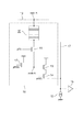
図2は、本実施形態に係る光電変換素子の一例を示す断面模式図である。光電変換素子には、光を電荷に変換する光電変換層1が、一対の電極である、アノード電極4とカソード電極5との間に配置されている。アノード電極の上には保護層7、波長選択部8、マイクロレンズ9が配置されている。カソード電極には、読み出し回路6が接続されている。
FIG. 2 is a schematic cross-sectional view showing an example of a photoelectric conversion element according to the present embodiment. In the photoelectric conversion element, a
一対の電極のうち基板に近い電極を下部電極と呼び、基板から遠い電極を上部電極と呼ぶことがある。下部電極はアノード電極であっても、カソード電極であってもよい。下部電極は、反射率が高い電極であってよい。電極が反射率の高い材料で構成されてもよいし、電極層に加えて反射層を有してもよい。 Of the pair of electrodes, the electrode closer to the substrate may be referred to as a lower electrode, and the electrode far from the substrate may be referred to as an upper electrode. The lower electrode may be an anode electrode or a cathode electrode. The lower electrode may be an electrode having a high reflectance. The electrode may be made of a material having high reflectance, or may have a reflective layer in addition to the electrode layer.
本発明に係る光電変換素子は、基板を有してよい。基板は、例えば、シリコン基板、ガラス基板、フレキシブル基板等を用いることができる。 The photoelectric conversion element according to the present invention may have a substrate. As the substrate, for example, a silicon substrate, a glass substrate, a flexible substrate, or the like can be used.
本発明に係る光電変換素子が有するカソード電極は、光電変換層で発生した電荷のうちの正孔を捕集する電極である。一方、アノード電極は、光電変換層で発生した電荷のうち電子を捕集する電極である。カソード電極およびアノード電極を構成する材料は導電性が高く、透明性を有していれば制限されない。カソード電極とアノード電極とを構成する材料は同じであっても異なってもよい。 The cathode electrode included in the photoelectric conversion element according to the present invention is an electrode that collects holes in the charges generated in the photoelectric conversion layer. On the other hand, the anode electrode is an electrode that collects electrons among the charges generated in the photoelectric conversion layer. The materials constituting the cathode electrode and the anode electrode are not limited as long as they have high conductivity and transparency. The materials constituting the cathode electrode and the anode electrode may be the same or different.
電極の材料は、具体的には、金属、金属酸化物、金属窒化物、金属硼化物、有機導電性化合物、これらの混合物等が挙げられ、更に具体的には、アンチモンやフッ素等をドープした酸化錫(ATO、FTO)、酸化錫、酸化亜鉛、酸化インジウム、酸化インジウム錫(ITO)、酸化亜鉛インジウム(IZO)等の導電性金属酸化物、金、銀、クロム、ニッケル、チタン、タングステン、アルミ等の金属及びこれらの金属の酸化物や窒化物などの導電性化合物(一例として窒化チタン(TiN)を挙げる)、更にこれらの金属と導電性金属酸化物との混合物又は積層物、ヨウ化銅、硫化銅などの無機導電性物質、ポリアニリン、ポリチオフェン、ポリピロールなどの有機導電性材料、及びこれらとITO又は窒化チタンとの積層物などが挙げられる。電極として特に好ましい材料は、窒化チタン、窒化モリブデン、窒化タンタル、窒化タングステンが挙げられる。 Specific examples of the electrode material include metals, metal oxides, metal nitrides, metal borohydrides, organic conductive compounds, and mixtures thereof, and more specifically, doping with antimony, fluorine, or the like. Conductive metal oxides such as tin oxide (ATO, FTO), tin oxide, zinc oxide, indium oxide, indium tin oxide (ITO), indium zinc oxide (IZO), gold, silver, chromium, nickel, titanium, tungsten, Metals such as aluminum and conductive compounds such as oxides and nitrides of these metals (titanium nitride (TiN) is taken as an example), and mixtures or laminates of these metals and conductive metal oxides, iodide. Examples thereof include inorganic conductive substances such as copper and copper sulfide, organic conductive materials such as polyaniline, polythiophene and polypyrrole, and laminates of these with ITO or titanium nitride. Particularly preferable materials for the electrode include titanium nitride, molybdenum nitride, tantalum nitride, and tungsten nitride.
本発明に係る光電変換素子が有する正孔または電子の捕集電極は、光電変換層で発生した電荷のいずれかを捕集する電極である。下部にある捕集電極は、撮像素子の構成においては画素電極であってよい。画素電極がカソードまたはアノードであることは、素子構成や下地の回路構成によって決められる。例えば基板上に基板/アノード電極/光電変換層/カソード電極の順でもよいし、基板/カソード電極/光電変換層/アノード電極の順でもよい。 The hole or electron collecting electrode included in the photoelectric conversion element according to the present invention is an electrode that collects any of the electric charges generated in the photoelectric conversion layer. The collection electrode at the bottom may be a pixel electrode in the configuration of the image pickup device. Whether the pixel electrode is a cathode or an anode is determined by the element configuration and the circuit configuration of the base. For example, the order may be substrate / anode electrode / photoelectric conversion layer / cathode electrode on the substrate, or the order may be substrate / cathode electrode / photoelectric conversion layer / anode electrode.
電極を形成する方法は、電極材料との適正を考慮して適宜選択することができる。具体的には、印刷方式、コーティング方式等の湿式方式、真空蒸着法、スパッタリング法、イオンプレーティング法等の物理的方式、CVD、プラズマCVD法等の化学的方式等により形成することができる。 The method for forming the electrode can be appropriately selected in consideration of the suitability with the electrode material. Specifically, it can be formed by a wet method such as a printing method or a coating method, a physical method such as a vacuum vapor deposition method, a sputtering method or an ion plating method, or a chemical method such as CVD or plasma CVD method.
電極がITOの場合、電子ビーム法、スパッタリング法、抵抗加熱蒸着法、化学反応法(ゾルーゲル法など)、酸化インジウムスズの分散物の塗布などの方法で形成することができる。更に、形成されたITOに、UV−オゾン処理、プラズマ処理などを施すことができる。電極がTiNの場合、反応性スパッタリング法をはじめとする各種の方法が用いられ、更にアニール処理、UV−オゾン処理、プラズマ処理などを施すことができる。 When the electrode is ITO, it can be formed by a method such as an electron beam method, a sputtering method, a resistance heating vapor deposition method, a chemical reaction method (sol-gel method or the like), or application of a dispersion of indium tin oxide. Further, the formed ITO can be subjected to UV-ozone treatment, plasma treatment and the like. When the electrode is TiN, various methods such as a reactive sputtering method are used, and further annealing treatment, UV-ozone treatment, plasma treatment and the like can be performed.
封止層として特に限定されるものではないが、無機材料により構成される。具体的には、酸化シリコン、窒化シリコン、窒化酸化シリコン、アルミニウム酸化物などがあげられる。酸化シリコン、窒化シリコン、窒化酸化シリコンは、スパッタリング法、CVD法により形成することができ、アルミニウム酸化物は、ALD法(原子層堆積法)により形成することができる。 The sealing layer is not particularly limited, but is composed of an inorganic material. Specific examples thereof include silicon oxide, silicon nitride, silicon nitride and aluminum oxide. Silicon oxide, silicon nitride, and silicon nitride can be formed by a sputtering method or a CVD method, and aluminum oxide can be formed by an ALD method (atomic layer deposition method).
封止層の封止性能は、水透過率が、10−5g/m2・day以下であればよい。封止層の層厚は特に限定されるものではないが、封止性能の観点から0.5μm以上であることが好ましい。一方で封止性能を保てるならば薄い方がよく、1μm以下であることが特に好ましい。 The sealing performance of the sealing layer may be such that the water transmittance is 10-5 g / m 2 · day or less. The layer thickness of the sealing layer is not particularly limited, but is preferably 0.5 μm or more from the viewpoint of sealing performance. On the other hand, if the sealing performance can be maintained, it is better to be thin, and it is particularly preferable that the thickness is 1 μm or less.
封止層が薄い方が好ましい理由は、撮像素子として用いる場合に、光電変換層からのカラーフィルタまでの距離が短いほど混色を低減させる効果があるためである。 The reason why a thinner sealing layer is preferable is that when used as an image sensor, the shorter the distance from the photoelectric conversion layer to the color filter, the more effective the color mixing is.
光電変換素子を作製する場合は、アニール工程を有することが好ましい。アニール温度は限定されないが、アニール温度の条件は150℃以上190℃以下であってよい。アニール温度は、アニール時間との兼ね合いで適宜決定してされる。 When manufacturing a photoelectric conversion element, it is preferable to have an annealing step. The annealing temperature is not limited, but the annealing temperature condition may be 150 ° C. or higher and 190 ° C. or lower. The annealing temperature is appropriately determined in consideration of the annealing time.
[実施形態に係る撮像素子]
本実施形態に係る撮像素子は、複数の画素を有し、画素は、本発明に係る光電変換素子と、光電変換素子に接続されている読み出しトランジスタを有する。
[Image sensor according to the embodiment]
The image pickup device according to the present embodiment has a plurality of pixels, and the pixels have a photoelectric conversion element according to the present invention and a readout transistor connected to the photoelectric conversion element.
複数の画素は、複数の行および複数の列を含む行列に配置されてよい。画素は、それぞれ信号処理回路に接続されてよい。信号処理回路は、各画素からの信号を受け取ることで、画像を得ることができる。 The plurality of pixels may be arranged in a matrix containing a plurality of rows and a plurality of columns. Each pixel may be connected to a signal processing circuit. The signal processing circuit can obtain an image by receiving a signal from each pixel.
読み出しトランジスタは、光電変換素子において生じた電荷に基づく信号を転送するトランジスタである。 The readout transistor is a transistor that transfers a signal based on the electric charge generated in the photoelectric conversion element.
信号処理回路は、CMOSセンサやCCDセンサであってよい。 The signal processing circuit may be a CMOS sensor or a CCD sensor.
撮像素子は、光フィルタを、例えばカラーフィルタを有してもよい。光電変換素子が、特定の波長の光に対応している場合、光電変換素子に対応したカラーフィルタを有することが好ましい。カラーフィルタは、1つの受光画素に1つのカラーフィルタを設けても、複数の受光画素に1つのカラーフィルタを設けてもよい。 The image pickup device may have an optical filter, for example, a color filter. When the photoelectric conversion element corresponds to light of a specific wavelength, it is preferable to have a color filter corresponding to the photoelectric conversion element. As the color filter, one color filter may be provided for one light receiving pixel, or one color filter may be provided for a plurality of light receiving pixels.
光フィルタは、カラーフィルタの他にも、赤外線以上の波長を透過するローパスフィルタ、紫外線以下の波長を透過するUVカットフィルタ等があげられる。 Examples of the optical filter include a low-pass filter that transmits wavelengths above infrared rays and a UV cut filter that transmits wavelengths below ultraviolet rays, in addition to color filters.
撮像素子は、マイクロレンズ等の光学部材を有してもよい。マイクロレンズは、外部からの光を光電変換部に集光するレンズである。マイクロレンズは、1つの受光画素に1つのマイクロレンズを設けてもよいし、複数の受光画素に対応する1つのマイクロレンズを設けてもよい。受光画素が複数設けられている場合は、複数の受光画素のそれぞれに1つずつマイクロレンズが設けられることが好ましい。 The image pickup device may have an optical member such as a microlens. A microlens is a lens that collects light from the outside on a photoelectric conversion unit. As the microlens, one microlens may be provided for one light receiving pixel, or one microlens corresponding to a plurality of light receiving pixels may be provided. When a plurality of light receiving pixels are provided, it is preferable that one microlens is provided for each of the plurality of light receiving pixels.
本発明に係る撮像素子は、撮像装置に用いることができる。撮像装置は、複数のレンズを有する撮像光学系と、撮像光学系を通過した光を受光する撮像素子と、を有する。また、撮像装置は、撮像素子と、撮像素子を収容する筐体と、を有し、筐体は撮像光学系と接合可能な接合部を有してよい。撮像装置はより具体的には、デジタルカメラまたはデジタルスチルカメラである。 The image pickup device according to the present invention can be used in an image pickup device. The image pickup apparatus includes an image pickup optical system having a plurality of lenses and an image pickup element that receives light that has passed through the image pickup optical system. Further, the image pickup apparatus may include an image pickup element and a housing for accommodating the image pickup element, and the housing may have a joint portion that can be joined to the image pickup optical system. More specifically, the image pickup device is a digital camera or a digital still camera.
また、撮像装置は、外部からの信号をする受信部をさらに有してもよい。受信部が受信する信号は、撮像装置の撮像範囲、撮像の開始、撮像の終了の少なくともいずれかを制御する信号である。また、撮像装置は、取得した画像を外部に送信する送信部をさらに有してもよい。取得した画像は例えば、撮像した画像、他の機器から送信された画像が挙げられる。 Further, the image pickup apparatus may further have a receiving unit for receiving a signal from the outside. The signal received by the receiving unit is a signal that controls at least one of the imaging range of the imaging device, the start of imaging, and the end of imaging. Further, the image pickup apparatus may further have a transmission unit for transmitting the acquired image to the outside. Examples of the acquired image include an captured image and an image transmitted from another device.
受信部や送信部を有することで、ネットワークカメラとして用いることができる。 By having a receiving unit and a transmitting unit, it can be used as a network camera.
図3は、本発明に係る光電変換装置を含む画素の回路図である。光電変換装置10は、nodeAで共通配線19に接続される。共通配線はグランドに接続されてよい。
FIG. 3 is a circuit diagram of a pixel including a photoelectric conversion device according to the present invention. The
画素18は、光電変換素子10と、光電変換部で生じた信号を読み出すための読み出し回路を含んでよい。読み出し回路は、例えば光電変換素子と電気的に接続した転送トランジスタ11、光電変換素子10と電気的に接続されたゲート電極を有する増幅トランジスタ13、情報が読み出される画素を選択する選択トランジスタ14、光電変換素子にリセット電圧を供給するリセットトランジスタ12を含んでよい。
The
転送トランジスタ11は、pTXでその転送を制御されてよい。リセットトランジスタは、pRESで電圧の供給を制御されてよい。選択トランジスタはpSELで選択または非選択の状態をとなる。
The
転送トランジスタ11、リセットトランジスタ12、増幅トランジスタ13は、nodeBで接続されている。構成によっては転送トランジスタを有さなくてもよい。
The
リセットトランジスタはnodeBの電位をリセットする電圧を供給するトランジスタである。リセットトランジスタのゲートにpRESを印加することで電圧の供給を制御できる。構成によってはリセットトランジスタを有さなくてもよい。 The reset transistor is a transistor that supplies a voltage that resets the potential of the nodeB. The voltage supply can be controlled by applying pRES to the gate of the reset transistor. Depending on the configuration, it is not necessary to have a reset transistor.
増幅トランジスタは、nodeBの電位に応じた電流を流すトランジスタである。増幅トランジスタは信号を出力する画素を選択する選択トランジスタ14に接続されている。選択トランジスタは、電流源16、列出力部15に接続されており、列出力部15は信号処理部に接続されてよい。
The amplification transistor is a transistor that allows a current to flow according to the potential of the nodeB. The amplification transistor is connected to a
選択トランジスタ14は、垂直出力信号線17に接続されている。垂直出力信号線17は、電流源16、列出力部15に接続されている。
The
図4は、本発明に係る撮像素子を表わす図である。撮像素子20は、複数の画素が2次元に配置されている撮像領域25と、周辺領域26とを有する。撮像領域以外領域は周辺領域である。周辺領域には、垂直走査回路21、読み出し回路22、水平走査回路23、出力アンプ24を有し、出力アンプは信号処理部27に接続されている。信号処理部は、読み出し回路に読みだされた情報により信号処理を行う信号処理部であり、CCD回路、CMOS回路等があげられる。
FIG. 4 is a diagram showing an image pickup device according to the present invention. The
読み出し回路22は、例えば、列アンプ、CDS回路、加算回路等を含み、垂直走査回路21によって選択された行の画素から垂直信号線を介して読み出された信号に対して増幅、加算等を行う。列アンプ、CDS回路、加算回路等は、例えば、画素列又は複数の画素列毎に配置される。水平走査回路23は、読み出し回路22の信号を順番に読み出すための信号を生成する。出力アンプ24は、水平走査回路23によって選択された列の信号を増幅して出力する。
The
以上の構成は、光電変換装置の一つの構成例に過ぎず、本実施形態は、これに限定されるものではない。読み出し回路22と水平走査回路23と出力アンプ24とは、2系統の出力経路を構成するため、撮像領域25を挟んで上下に1つずつ配置されている。しかし、出力経路は3つ以上設けられていてもよい。各出力アンプから出力された信号は信号処理部で画像信号として合成される。
The above configuration is merely one configuration example of the photoelectric conversion device, and the present embodiment is not limited to this. The
[第一の有機化合物の材料の酸化電位の測定]
酸化電位などの電気化学特性の評価は、サリクリックボルタンメトリー(CV)によって行うことができる。
[Measurement of oxidation potential of the material of the first organic compound]
Evaluation of electrochemical properties such as oxidation potential can be performed by salicic voltammetry (CV).
CV測定サンプルは、0.1Mテトラブチルアンモニウム過塩素酸塩のオルトジクロロベンゼン溶液10mLに第一の有機化合物を1mg程度溶解させ、窒素による脱気処理を行うことにより調製した。CV測定には三電極法を用い、各電極には、非水溶媒系Ag/Ag+参照電極、直径0.5mm、長さ5cmの白金カウンター電極、内径3mmのガラス状カーボン作用電極(いずれもビー・エー・エス株式会社製)を用いた。電気化学測定装置には、ALS社製のモデル660C、電気化学アナライザーを用いた。測定の挿引速度は、0.1V/sとした。図5は、化合物の酸化電位および還元電位を決定するサイクリックボルタモグラムの一例である。サイクリックボルタモグラムのピーク値から酸化電位および還元電位を見積もることができる。本明細書においては、酸化電位はEox、還元電位はEredと記す。 The CV measurement sample was prepared by dissolving about 1 mg of the first organic compound in 10 mL of an orthodichlorobenzene solution of 0.1 M tetrabutylammonium perchlorate and degassing with nitrogen. The three-electrode method is used for CV measurement, and each electrode is a non-aqueous solvent-based Ag / Ag + reference electrode, a platinum counter electrode with a diameter of 0.5 mm and a length of 5 cm, and a glassy carbon working electrode with an inner diameter of 3 mm (all). BAS Co., Ltd.) was used. As the electrochemical measuring device, a model 660C manufactured by ALS and an electrochemical analyzer were used. The insertion speed of the measurement was 0.1 V / s. FIG. 5 is an example of a cyclic voltammogram that determines the oxidation and reduction potentials of a compound. The oxidation potential and reduction potential can be estimated from the peak value of the cyclic voltammogram. In the present specification, the oxidation potential is referred to as Exo, and the reduction potential is referred to as Red.
表1は、第一の有機化合物の例示化合物の酸化電位である。表1の記載は、第一の有機化合物の例示化合物番号に対応している。 Table 1 shows the oxidation potentials of the exemplary compounds of the first organic compound. The description in Table 1 corresponds to the exemplary compound number of the first organic compound.
[実施例1]
本実施例では、ΔE≧1.79Vとなる第一の有機化合物と第二の有機化合物との組み合わせを用いて光電変換素子を作製した。作製した光電変換素子を用いて暗電流を測定した。
[Example 1]
In this example, a photoelectric conversion element was manufactured by using a combination of the first organic compound and the second organic compound having ΔE ≧ 1.79V. The dark current was measured using the manufactured photoelectric conversion element.
本実施例において、Si基板の上に光電変換素子を形成した。光電変換素子は、カソード電極、電子ブロック層、光電変換層、正孔ブロック層、アノード電極が順次形成されている。 In this embodiment, a photoelectric conversion element is formed on a Si substrate. In the photoelectric conversion element, a cathode electrode, an electron block layer, a photoelectric conversion layer, a hole block layer, and an anode electrode are sequentially formed.
本実施例において、光電変換素子は以下の工程により作製した。 In this embodiment, the photoelectric conversion element was manufactured by the following steps.
まず、配線層、絶縁層、が積層されており各画素に対応する箇所に配線層からコンタクトホールが絶縁層に開口を設けて導通可能なように形成されているSi基板を準備した。このコンタクトホールは、基板端のパッド部と配線によって接続されている。このコンタクトホール部に重なるようにIZO電極をスパッタリング法により形成した。パターニングを行い3mm2となるIZO電極(カソード電極)を形成した。このときIZO電極の膜厚を100nmとした。 First, a Si substrate was prepared in which a wiring layer and an insulating layer were laminated, and contact holes were provided in the insulating layer from the wiring layer at locations corresponding to each pixel so as to be conductive. This contact hole is connected to the pad portion at the end of the board by wiring. The IZO electrode was formed by a sputtering method so as to overlap the contact hole portion. Patterning was performed to form an IZO electrode (cathode electrode) having a size of 3 mm 2. At this time, the film thickness of the IZO electrode was set to 100 nm.
上記IZO電極上に、有機化合物層を真空蒸着法で形成した。層構成、層厚は下記表2の通りである。次にアノード電極として、IZOをスパッタリング法で形成した。アノード電極の厚さは30nmとした。 An organic compound layer was formed on the IZO electrode by a vacuum vapor deposition method. The layer structure and layer thickness are shown in Table 2 below. Next, IZO was formed as an anode electrode by a sputtering method. The thickness of the anode electrode was 30 nm.
光電変換素子の層構成を表2に示す。 Table 2 shows the layer structure of the photoelectric conversion element.
なお、表2は、下部電極であるカソードが表の下側になるよう記載したものである。 In Table 2, the cathode, which is the lower electrode, is shown so as to be on the lower side of the table.
電子ブロック層には以下の化合物(d−1)を用いた。 The following compound (d-1) was used for the electron block layer.
光電変換層の第一の有機化合物には例示化合物1−1乃至3−14、正孔ブロック層にはフラーレンC60(d−2)、およびC70(d−3)と下記の有機化合物(d−4)のいずれかを用いた。 Exemplified compounds 1-1 to 3-14 are used as the first organic compound in the photoelectric conversion layer, fullerenes C60 (d-2) and C70 (d-3) are used as the hole block layer, and the following organic compounds (d-) are used. Any of 4) was used.
なお、d−2,d−3、d−4の還元電位は表3の通りである。 The reduction potentials of d-2, d-3, and d-4 are shown in Table 3.
上部電極を形成後、ガラスキャップと紫外線効果樹脂を使って中空封止を行った。このようにして得られた素子は170℃のホットプレート上で封止面を上向きとして1時間程度アニールした。 After forming the upper electrode, hollow sealing was performed using a glass cap and an ultraviolet effect resin. The device thus obtained was annealed on a hot plate at 170 ° C. with the sealing surface facing upward for about 1 hour.
得られた素子について、光電変換素子の特性を測定・評価した。素子に5V印加時の電流を確認したところ、いずれの素子でも明所での電流値が暗所での電流値の10倍以上の値であるため光電変換素子が機能していることを確認した。 The characteristics of the photoelectric conversion element were measured and evaluated for the obtained element. When the current when 5V was applied to the element was confirmed, it was confirmed that the photoelectric conversion element was functioning because the current value in the bright place was 10 times or more the current value in the dark place in any element. ..
光電変換素子の暗電流の測定においては、60℃の恒温槽内に保持し半導体パラメータアナライザー(Agilent社4155C)に配線されたプロバーを電極にコンタクトさせて測定した。 In the measurement of the dark current of the photoelectric conversion element, a prober held in a constant temperature bath at 60 ° C. and wired to a semiconductor parameter analyzer (Agilent Co., Ltd. 4155C) was brought into contact with the electrode for measurement.
暗電流評価の基準は以下の通りとした。 The criteria for dark current evaluation are as follows.
A:100pA/cm2未満
B:100pA/cm2以上1000pA/cm2未満
C:1000pA/cm2以上
Aは良好、B及びCは不良とした。
A: 100 pA / cm less than 2 B: 100 pA / cm 2 or more and less than 1000 pA / cm 2 C: 1000 pA / cm 2 or more A is good and B and C are bad.
本実施例の光電変換素子の暗電流評価はAであった。例えば10μm角の画素とした場合の面積は1.0×10⁻⁶cm2である。この光電変換素子を撮像素子に用いた場合、低暗電流の撮像素子を得ることができる。この低暗電流特性が撮像素子のノイズの低減につながる。 The dark current evaluation of the photoelectric conversion element of this embodiment was A. For example, the area of a 10 μm square pixel is 1.0 × 10⁻⁶ cm 2 . When this photoelectric conversion element is used as an image pickup device, an image pickup device having a low dark current can be obtained. This low dark current characteristic leads to reduction of noise in the image sensor.
[実施例2乃至15]
第一の有機化合物及び第二の有機化合物の組み合わせを表4に示す組み合わせとする以外は、実施例1と同様に光電変換素子を作製した。実施例1乃至15についての結果を次の表4に示す。
[Examples 2 to 15]
A photoelectric conversion element was produced in the same manner as in Example 1 except that the combination of the first organic compound and the second organic compound was the combination shown in Table 4. The results for Examples 1 to 15 are shown in Table 4 below.
[比較例1乃至9]
第一の有機化合物と第二の有機化合物の組み合わせを表5の組み合わせとする以外は実施例1と同様に光電変換素子を作製した。表5の化合物の組み合わせは、ΔE<1.79Vの組み合わせである。作製した光電変換素子を実施例1と同様の測定法で暗電流評価を行った。
[Comparative Examples 1 to 9]
A photoelectric conversion element was produced in the same manner as in Example 1 except that the combination of the first organic compound and the second organic compound was the combination shown in Table 5. The combination of compounds in Table 5 is a combination of ΔE <1.79V. The prepared photoelectric conversion element was evaluated for dark current by the same measurement method as in Example 1.
比較例8に用いたe−1の構造は以下の通りである。 The structure of e-1 used in Comparative Example 8 is as follows.
ΔEが1.79V以上の光電変換素子は、暗電流の評価がA以上の結果であり、低い暗電流特性が得られた。 For the photoelectric conversion element having ΔE of 1.79 V or more, the evaluation of dark current was A or higher, and low dark current characteristics were obtained.
[実施例16]
実施例1において作製した光電変換素子を用いて、暗電流の温度依存性を測定した。図6は、実施例1の光電変換素子のアレニウスプロットである。縦軸は、60℃における暗電流値で規格化した暗電流値である。縦軸の目盛は常用対数である。横軸は絶対温度の逆数である。図6において60℃付近から高温側に向かって傾きの絶対値が大きくなる。この傾きから次式(5)に従い活性化エネルギーを求めた。
[Example 16]
The temperature dependence of the dark current was measured using the photoelectric conversion element produced in Example 1. FIG. 6 is an Arrhenius plot of the photoelectric conversion element of the first embodiment. The vertical axis is the dark current value normalized by the dark current value at 60 ° C. The scale on the vertical axis is the common logarithm. The horizontal axis is the reciprocal of the absolute temperature. In FIG. 6, the absolute value of the inclination increases from the vicinity of 60 ° C. toward the high temperature side. From this slope, the activation energy was obtained according to the following equation (5).
ここで、T:絶対温度、kB:ボルツマン定数、Ea:活性化エネルギー、J:温度Tでの電流値、J0:頻度因子である。この傾きから暗電流の活性化エネルギーは0.84eVと求めた。 Here, T: absolute temperature, k B : Boltzmann constant, E a : activation energy, J: current value at temperature T, J 0 : frequency factor. From this slope, the activation energy of dark current was determined to be 0.84 eV.
[実施例17]
例示化合物1−3、1−7、1−13、1−21、1−23を第一の有機化合物とした以外は実施例1と同様に光電変換素子を作製し、実施例16と同様に暗電流の活性化エネルギーを求めた。図7は活性化エネルギー(Ea)とΔEとの関係を示した図である。図7より、ΔEが1.79V以上となることで、活性化エネルギーが大きくなることがわかる。これは、ΔEが1.79V以上である場合、熱励起による電荷発生確率が低下することを指す。
[Example 17]
An photoelectric conversion element was produced in the same manner as in Example 1 except that the exemplified compounds 1-3, 1-7, 1-13, 1-21, and 1-23 were used as the first organic compound, and the same as in Example 16. The activation energy of the dark current was obtained. FIG. 7 is a diagram showing the relationship between the activation energy (Ea) and ΔE. From FIG. 7, it can be seen that the activation energy increases when ΔE becomes 1.79 V or more. This means that when ΔE is 1.79 V or more, the probability of charge generation due to thermal excitation decreases.
[実施例18]
封止層にCVD法による窒化珪素層を用いた以外は、実施例1と同様にして光電変換素子を作製した。窒化珪素層は1μmの層厚で形成した。この素子に365nmのLED光を1W/cm2の強度で24h照射して耐久性を評価した。
[Example 18]
A photoelectric conversion element was produced in the same manner as in Example 1 except that a silicon nitride layer by the CVD method was used as the sealing layer. The silicon nitride layer was formed with a layer thickness of 1 μm. This element was irradiated with LED light of 365 nm at an intensity of 1 W /
形成したSiN(1μm)の365nmの吸収率は75%であった。この素子は24h後においても、暗電流の値は変化しなかった。 The absorption rate of the formed SiN (1 μm) at 365 nm was 75%. The dark current value of this device did not change even after 24 hours.
一方、実施例1で作製した光電変換素子は、24時間の光照射後に約10%程度暗電流が上昇した。ガラスキャップは紫外線を吸収率がSiNよりも小さいためである。これを考慮すると、紫外線の吸収可能な材質により封止層を設けることが好ましい。 On the other hand, in the photoelectric conversion element produced in Example 1, the dark current increased by about 10% after irradiation with light for 24 hours. This is because the glass cap absorbs ultraviolet rays less than SiN. Considering this, it is preferable to provide a sealing layer with a material capable of absorbing ultraviolet rays.
以上のことから本発明に係る光電変換素子は、暗電流が低減された光電変換素子である。これを有する撮像素子は、光電変換素子部に由来する暗電流ノイズが少ないので好ましい。 From the above, the photoelectric conversion element according to the present invention is a photoelectric conversion element having a reduced dark current. An image pickup device having this is preferable because it has less dark current noise derived from the photoelectric conversion element portion.
1 光電変換層
2 正孔ブロック層
3 電子ブロック層
4 アノード電極
5 カソード電極
6 読み出し回路
7 保護層
8 カラーフィルタ
9 マイクロレンズ
1
Claims (13)
前記光電変換層は、第一の有機化合物と、第二の有機化合物とを有し、
前記第一の有機化合物の酸化電位は、前記第二の有機化合物の酸化電位よりも小さく、
下記式(A)で表されるΔEが、下記式(B)を満たし、
前記第一の有機化合物が下記構造式で表されることを特徴とする光電変換素子。
ΔE=第一の有機化合物の酸化電位−第二の有機化合物の還元電位 (A)
ΔE≧1.79 [V] (B)
The photoelectric conversion layer has a first organic compound and a second organic compound .
The oxidation potential of the first organic compound is smaller than the oxidation potential of the second organic compound.
ΔE represented by the following formula (A) is, meets the following formula (B),
A photoelectric conversion element characterized in that the first organic compound is represented by the following structural formula.
ΔE = Oxidation potential of the first organic compound-Reduction potential of the second organic compound (A)
ΔE ≧ 1.79 [V] (B)
前記画素は、請求項1乃至8のいずれか一項に記載の光電変換素子と、前記光電変換素子に接続されている読み出し回路と、を有することを特徴とする撮像素子。 An image pickup device having a plurality of pixels and a signal processing circuit connected to the pixels.
The pixel is an image pickup device comprising the photoelectric conversion element according to any one of claims 1 to 8 and a readout circuit connected to the photoelectric conversion element.
前記撮像素子は、請求項9に記載の撮像素子であることを特徴とする撮像装置。 An image pickup apparatus having an optical unit having a plurality of lenses and an image pickup element that receives light transmitted through the optical unit.
The image pickup device according to claim 9 , wherein the image pickup device is the image pickup device.
Priority Applications (2)
| Application Number | Priority Date | Filing Date | Title |
|---|---|---|---|
| JP2016220715A JP6971561B2 (en) | 2016-11-11 | 2016-11-11 | Photoelectric conversion element, image sensor and image sensor |
| US15/806,004 US10468614B2 (en) | 2016-11-11 | 2017-11-07 | Photoelectric conversion element, image pick-up element, and image pick-up apparatus |
Applications Claiming Priority (1)
| Application Number | Priority Date | Filing Date | Title |
|---|---|---|---|
| JP2016220715A JP6971561B2 (en) | 2016-11-11 | 2016-11-11 | Photoelectric conversion element, image sensor and image sensor |
Publications (2)
| Publication Number | Publication Date |
|---|---|
| JP2018078241A JP2018078241A (en) | 2018-05-17 |
| JP6971561B2 true JP6971561B2 (en) | 2021-11-24 |
Family
ID=62108942
Family Applications (1)
| Application Number | Title | Priority Date | Filing Date |
|---|---|---|---|
| JP2016220715A Active JP6971561B2 (en) | 2016-11-11 | 2016-11-11 | Photoelectric conversion element, image sensor and image sensor |
Country Status (2)
| Country | Link |
|---|---|
| US (1) | US10468614B2 (en) |
| JP (1) | JP6971561B2 (en) |
Family Cites Families (7)
| Publication number | Priority date | Publication date | Assignee | Title |
|---|---|---|---|---|
| JP4677314B2 (en) | 2005-09-20 | 2011-04-27 | 富士フイルム株式会社 | Sensor and organic photoelectric conversion element driving method |
| US20070272918A1 (en) * | 2006-05-25 | 2007-11-29 | Barry Rand | Organic photosensitive devices using subphthalocyanine compounds |
| JP4604128B2 (en) | 2008-10-15 | 2010-12-22 | 富士フイルム株式会社 | Photoelectric conversion element and imaging element |
| JP2011199263A (en) * | 2010-02-25 | 2011-10-06 | Fujifilm Corp | Photoelectric conversion device, imaging device, method of manufacturing the same, and imaging apparatus |
| EP2924020B1 (en) * | 2012-11-21 | 2019-01-16 | LG Chem, Ltd. | Fluoranthene compound, and organic electronic device comprising same |
| CN107068871A (en) * | 2013-03-11 | 2017-08-18 | 沙特基础工业公司 | Plane donor-acceptor hetero-junctions and the photovoltaic cell comprising it |
| JP6500786B2 (en) * | 2014-02-14 | 2019-04-17 | 東洋紡株式会社 | Organic semiconductor material |
-
2016
- 2016-11-11 JP JP2016220715A patent/JP6971561B2/en active Active
-
2017
- 2017-11-07 US US15/806,004 patent/US10468614B2/en active Active
Also Published As
| Publication number | Publication date |
|---|---|
| US10468614B2 (en) | 2019-11-05 |
| US20180138432A1 (en) | 2018-05-17 |
| JP2018078241A (en) | 2018-05-17 |
Similar Documents
| Publication | Publication Date | Title |
|---|---|---|
| Sutherland et al. | Sensitive, fast, and stable perovskite photodetectors exploiting interface engineering | |
| Lee et al. | Green-sensitive organic photodetectors with high sensitivity and spectral selectivity using subphthalocyanine derivatives | |
| JP7102114B2 (en) | Photoelectric conversion element, image sensor and image sensor | |
| Yang et al. | Mitigating dark current for high-performance near-infrared organic photodiodes via charge blocking and defect passivation | |
| JP6645700B2 (en) | Organic photoelectric conversion element, two-dimensional sensor, image sensor, and imaging device | |
| KR101884021B1 (en) | Photoelectric conversion element, solid-state imaging element, imaging apparatus, and method for manufacturing photoelectric conversion element | |
| JP6833351B2 (en) | Organic photoelectric conversion element, optical area sensor, image sensor and image sensor | |
| Han et al. | Perovskite/poly [bis (4-phenyl)(2, 4, 6-trimethylphenyl) amine] bulk heterojunction for high-efficient carbon-based large-area solar cells by gradient engineering | |
| CN110301052B (en) | Photoelectric conversion element, and optical area sensor, image pickup element, and image pickup apparatus using the same | |
| JP2022021347A (en) | Organic compound, and organic photoelectric conversion element | |
| WO2017138363A1 (en) | Organic photoelectric conversion element, optical area sensor, imaging element and imaging device | |
| JP7013163B2 (en) | Organic compounds and photoelectric conversion elements | |
| US20190267545A1 (en) | Photoelectric conversion element, and imaging element and imaging apparatus including the same | |
| US11711931B2 (en) | Photoelectric conversion element, measuring method of the same, solid-state imaging device, electronic device, and solar cell | |
| JP2019099570A (en) | Fullerene derivatives, and thin film, photoelectric element, image sensor and electronic device comprising the same | |
| JP6932564B2 (en) | Organic photoelectric conversion element, image sensor and image sensor | |
| US20200136063A1 (en) | Compound and film and photoelectric diode and organic sensor and electronic device | |
| WO2018147202A1 (en) | Photoelectric conversion element, optical area sensor using same, imaging element, and imaging device | |
| JP6971561B2 (en) | Photoelectric conversion element, image sensor and image sensor | |
| JP2015103598A (en) | Organic functional layer-equipped substrate and method of manufacturing the same | |
| WO2018088325A1 (en) | Photoelectric conversion element, imaging element and imaging device | |
| WO2022064984A1 (en) | Cyanine compound and photoelectric conversion element | |
| JP7039285B2 (en) | Photoelectric conversion element, optical area sensor using it, image sensor, image sensor | |
| JP2018078240A (en) | Photoelectric conversion element, image pick-up device having the same and imaging apparatus | |
| JP2019006718A (en) | Organic compound, organic electronic device having the same, photoelectric conversion element having the same, imaging element and imaging device |
Legal Events
| Date | Code | Title | Description |
|---|---|---|---|
| A621 | Written request for application examination |
Free format text: JAPANESE INTERMEDIATE CODE: A621 Effective date: 20191007 |
|
| A131 | Notification of reasons for refusal |
Free format text: JAPANESE INTERMEDIATE CODE: A131 Effective date: 20200825 |
|
| A977 | Report on retrieval |
Free format text: JAPANESE INTERMEDIATE CODE: A971007 Effective date: 20200826 |
|
| A521 | Request for written amendment filed |
Free format text: JAPANESE INTERMEDIATE CODE: A523 Effective date: 20201022 |
|
| A131 | Notification of reasons for refusal |
Free format text: JAPANESE INTERMEDIATE CODE: A131 Effective date: 20210406 |
|
| A521 | Request for written amendment filed |
Free format text: JAPANESE INTERMEDIATE CODE: A523 Effective date: 20210525 |
|
| TRDD | Decision of grant or rejection written | ||
| A01 | Written decision to grant a patent or to grant a registration (utility model) |
Free format text: JAPANESE INTERMEDIATE CODE: A01 Effective date: 20211005 |
|
| A61 | First payment of annual fees (during grant procedure) |
Free format text: JAPANESE INTERMEDIATE CODE: A61 Effective date: 20211102 |
|
| R151 | Written notification of patent or utility model registration |
Ref document number: 6971561 Country of ref document: JP Free format text: JAPANESE INTERMEDIATE CODE: R151 |