JP6967371B2 - Active matrix substrate - Google Patents
Active matrix substrate Download PDFInfo
- Publication number
- JP6967371B2 JP6967371B2 JP2017104518A JP2017104518A JP6967371B2 JP 6967371 B2 JP6967371 B2 JP 6967371B2 JP 2017104518 A JP2017104518 A JP 2017104518A JP 2017104518 A JP2017104518 A JP 2017104518A JP 6967371 B2 JP6967371 B2 JP 6967371B2
- Authority
- JP
- Japan
- Prior art keywords
- insulating film
- film
- substrate
- metal wiring
- electrode
- Prior art date
- Legal status (The legal status is an assumption and is not a legal conclusion. Google has not performed a legal analysis and makes no representation as to the accuracy of the status listed.)
- Active
Links
- 239000000758 substrate Substances 0.000 title claims description 104
- 239000011159 matrix material Substances 0.000 title claims description 10
- 229910052751 metal Inorganic materials 0.000 claims description 47
- 239000002184 metal Substances 0.000 claims description 47
- 230000002093 peripheral effect Effects 0.000 claims description 14
- 239000004065 semiconductor Substances 0.000 claims description 12
- 239000004642 Polyimide Substances 0.000 claims description 5
- 229920001721 polyimide Polymers 0.000 claims description 5
- 239000010408 film Substances 0.000 description 196
- 239000004973 liquid crystal related substance Substances 0.000 description 68
- 239000011347 resin Substances 0.000 description 66
- 229920005989 resin Polymers 0.000 description 66
- 239000000463 material Substances 0.000 description 33
- 238000000034 method Methods 0.000 description 12
- 230000005684 electric field Effects 0.000 description 11
- XLOMVQKBTHCTTD-UHFFFAOYSA-N Zinc monoxide Chemical compound [Zn]=O XLOMVQKBTHCTTD-UHFFFAOYSA-N 0.000 description 9
- 239000002245 particle Substances 0.000 description 7
- 238000012545 processing Methods 0.000 description 7
- 239000007769 metal material Substances 0.000 description 6
- 239000000049 pigment Substances 0.000 description 6
- 239000010409 thin film Substances 0.000 description 6
- 230000004888 barrier function Effects 0.000 description 5
- 238000005401 electroluminescence Methods 0.000 description 4
- 239000011521 glass Substances 0.000 description 4
- 230000007935 neutral effect Effects 0.000 description 4
- 230000008569 process Effects 0.000 description 4
- 230000001681 protective effect Effects 0.000 description 4
- 239000011787 zinc oxide Substances 0.000 description 4
- VYPSYNLAJGMNEJ-UHFFFAOYSA-N Silicium dioxide Chemical compound O=[Si]=O VYPSYNLAJGMNEJ-UHFFFAOYSA-N 0.000 description 3
- 230000000694 effects Effects 0.000 description 3
- 230000014509 gene expression Effects 0.000 description 3
- 229910052738 indium Inorganic materials 0.000 description 3
- APFVFJFRJDLVQX-UHFFFAOYSA-N indium atom Chemical compound [In] APFVFJFRJDLVQX-UHFFFAOYSA-N 0.000 description 3
- 229910010272 inorganic material Inorganic materials 0.000 description 3
- 229910052814 silicon oxide Inorganic materials 0.000 description 3
- 238000002834 transmittance Methods 0.000 description 3
- 229910052581 Si3N4 Inorganic materials 0.000 description 2
- HCHKCACWOHOZIP-UHFFFAOYSA-N Zinc Chemical compound [Zn] HCHKCACWOHOZIP-UHFFFAOYSA-N 0.000 description 2
- 230000009471 action Effects 0.000 description 2
- 210000004027 cell Anatomy 0.000 description 2
- 238000011161 development Methods 0.000 description 2
- 230000018109 developmental process Effects 0.000 description 2
- AJNVQOSZGJRYEI-UHFFFAOYSA-N digallium;oxygen(2-) Chemical compound [O-2].[O-2].[O-2].[Ga+3].[Ga+3] AJNVQOSZGJRYEI-UHFFFAOYSA-N 0.000 description 2
- 229910001195 gallium oxide Inorganic materials 0.000 description 2
- 230000012447 hatching Effects 0.000 description 2
- AMGQUBHHOARCQH-UHFFFAOYSA-N indium;oxotin Chemical compound [In].[Sn]=O AMGQUBHHOARCQH-UHFFFAOYSA-N 0.000 description 2
- 150000002484 inorganic compounds Chemical class 0.000 description 2
- 230000003287 optical effect Effects 0.000 description 2
- HQVNEWCFYHHQES-UHFFFAOYSA-N silicon nitride Chemical compound N12[Si]34N5[Si]62N3[Si]51N64 HQVNEWCFYHHQES-UHFFFAOYSA-N 0.000 description 2
- 229910052725 zinc Inorganic materials 0.000 description 2
- 239000011701 zinc Substances 0.000 description 2
- 239000004925 Acrylic resin Substances 0.000 description 1
- 229920000178 Acrylic resin Polymers 0.000 description 1
- OKTJSMMVPCPJKN-UHFFFAOYSA-N Carbon Chemical compound [C] OKTJSMMVPCPJKN-UHFFFAOYSA-N 0.000 description 1
- GYHNNYVSQQEPJS-UHFFFAOYSA-N Gallium Chemical compound [Ga] GYHNNYVSQQEPJS-UHFFFAOYSA-N 0.000 description 1
- ZOKXTWBITQBERF-UHFFFAOYSA-N Molybdenum Chemical compound [Mo] ZOKXTWBITQBERF-UHFFFAOYSA-N 0.000 description 1
- 239000004952 Polyamide Substances 0.000 description 1
- RTAQQCXQSZGOHL-UHFFFAOYSA-N Titanium Chemical compound [Ti] RTAQQCXQSZGOHL-UHFFFAOYSA-N 0.000 description 1
- 229910007717 ZnSnO Inorganic materials 0.000 description 1
- NIXOWILDQLNWCW-UHFFFAOYSA-N acrylic acid group Chemical group C(C=C)(=O)O NIXOWILDQLNWCW-UHFFFAOYSA-N 0.000 description 1
- 229910021417 amorphous silicon Inorganic materials 0.000 description 1
- 239000011230 binding agent Substances 0.000 description 1
- 239000001055 blue pigment Substances 0.000 description 1
- 229910052799 carbon Inorganic materials 0.000 description 1
- 238000004040 coloring Methods 0.000 description 1
- 238000002788 crimping Methods 0.000 description 1
- 210000002858 crystal cell Anatomy 0.000 description 1
- 238000013461 design Methods 0.000 description 1
- 230000009977 dual effect Effects 0.000 description 1
- 238000001962 electrophoresis Methods 0.000 description 1
- 238000005530 etching Methods 0.000 description 1
- 229910052733 gallium Inorganic materials 0.000 description 1
- 239000001056 green pigment Substances 0.000 description 1
- 239000011147 inorganic material Substances 0.000 description 1
- 238000009413 insulation Methods 0.000 description 1
- 229910052750 molybdenum Inorganic materials 0.000 description 1
- 239000011733 molybdenum Substances 0.000 description 1
- KYKLWYKWCAYAJY-UHFFFAOYSA-N oxotin;zinc Chemical compound [Zn].[Sn]=O KYKLWYKWCAYAJY-UHFFFAOYSA-N 0.000 description 1
- 229920002647 polyamide Polymers 0.000 description 1
- 239000004417 polycarbonate Substances 0.000 description 1
- 229920000515 polycarbonate Polymers 0.000 description 1
- 239000001054 red pigment Substances 0.000 description 1
- 230000004044 response Effects 0.000 description 1
- 239000003566 sealing material Substances 0.000 description 1
- 230000003595 spectral effect Effects 0.000 description 1
- 229910052715 tantalum Inorganic materials 0.000 description 1
- GUVRBAGPIYLISA-UHFFFAOYSA-N tantalum atom Chemical compound [Ta] GUVRBAGPIYLISA-UHFFFAOYSA-N 0.000 description 1
- 238000012360 testing method Methods 0.000 description 1
- 229910052719 titanium Inorganic materials 0.000 description 1
- 239000010936 titanium Substances 0.000 description 1
- YVTHLONGBIQYBO-UHFFFAOYSA-N zinc indium(3+) oxygen(2-) Chemical compound [O--].[Zn++].[In+3] YVTHLONGBIQYBO-UHFFFAOYSA-N 0.000 description 1
Images


Classifications
-
- H—ELECTRICITY
- H01—ELECTRIC ELEMENTS
- H01L—SEMICONDUCTOR DEVICES NOT COVERED BY CLASS H10
- H01L27/00—Devices consisting of a plurality of semiconductor or other solid-state components formed in or on a common substrate
- H01L27/02—Devices consisting of a plurality of semiconductor or other solid-state components formed in or on a common substrate including semiconductor components specially adapted for rectifying, oscillating, amplifying or switching and having at least one potential-jump barrier or surface barrier; including integrated passive circuit elements with at least one potential-jump barrier or surface barrier
- H01L27/12—Devices consisting of a plurality of semiconductor or other solid-state components formed in or on a common substrate including semiconductor components specially adapted for rectifying, oscillating, amplifying or switching and having at least one potential-jump barrier or surface barrier; including integrated passive circuit elements with at least one potential-jump barrier or surface barrier the substrate being other than a semiconductor body, e.g. an insulating body
- H01L27/1214—Devices consisting of a plurality of semiconductor or other solid-state components formed in or on a common substrate including semiconductor components specially adapted for rectifying, oscillating, amplifying or switching and having at least one potential-jump barrier or surface barrier; including integrated passive circuit elements with at least one potential-jump barrier or surface barrier the substrate being other than a semiconductor body, e.g. an insulating body comprising a plurality of TFTs formed on a non-semiconducting substrate, e.g. driving circuits for AMLCDs
- H01L27/124—Devices consisting of a plurality of semiconductor or other solid-state components formed in or on a common substrate including semiconductor components specially adapted for rectifying, oscillating, amplifying or switching and having at least one potential-jump barrier or surface barrier; including integrated passive circuit elements with at least one potential-jump barrier or surface barrier the substrate being other than a semiconductor body, e.g. an insulating body comprising a plurality of TFTs formed on a non-semiconducting substrate, e.g. driving circuits for AMLCDs with a particular composition, shape or layout of the wiring layers specially adapted to the circuit arrangement, e.g. scanning lines in LCD pixel circuits
-
- G—PHYSICS
- G02—OPTICS
- G02F—OPTICAL DEVICES OR ARRANGEMENTS FOR THE CONTROL OF LIGHT BY MODIFICATION OF THE OPTICAL PROPERTIES OF THE MEDIA OF THE ELEMENTS INVOLVED THEREIN; NON-LINEAR OPTICS; FREQUENCY-CHANGING OF LIGHT; OPTICAL LOGIC ELEMENTS; OPTICAL ANALOGUE/DIGITAL CONVERTERS
- G02F1/00—Devices or arrangements for the control of the intensity, colour, phase, polarisation or direction of light arriving from an independent light source, e.g. switching, gating or modulating; Non-linear optics
- G02F1/01—Devices or arrangements for the control of the intensity, colour, phase, polarisation or direction of light arriving from an independent light source, e.g. switching, gating or modulating; Non-linear optics for the control of the intensity, phase, polarisation or colour
- G02F1/13—Devices or arrangements for the control of the intensity, colour, phase, polarisation or direction of light arriving from an independent light source, e.g. switching, gating or modulating; Non-linear optics for the control of the intensity, phase, polarisation or colour based on liquid crystals, e.g. single liquid crystal display cells
- G02F1/133—Constructional arrangements; Operation of liquid crystal cells; Circuit arrangements
- G02F1/1333—Constructional arrangements; Manufacturing methods
- G02F1/133305—Flexible substrates, e.g. plastics, organic film
-
- G—PHYSICS
- G02—OPTICS
- G02F—OPTICAL DEVICES OR ARRANGEMENTS FOR THE CONTROL OF LIGHT BY MODIFICATION OF THE OPTICAL PROPERTIES OF THE MEDIA OF THE ELEMENTS INVOLVED THEREIN; NON-LINEAR OPTICS; FREQUENCY-CHANGING OF LIGHT; OPTICAL LOGIC ELEMENTS; OPTICAL ANALOGUE/DIGITAL CONVERTERS
- G02F1/00—Devices or arrangements for the control of the intensity, colour, phase, polarisation or direction of light arriving from an independent light source, e.g. switching, gating or modulating; Non-linear optics
- G02F1/01—Devices or arrangements for the control of the intensity, colour, phase, polarisation or direction of light arriving from an independent light source, e.g. switching, gating or modulating; Non-linear optics for the control of the intensity, phase, polarisation or colour
- G02F1/13—Devices or arrangements for the control of the intensity, colour, phase, polarisation or direction of light arriving from an independent light source, e.g. switching, gating or modulating; Non-linear optics for the control of the intensity, phase, polarisation or colour based on liquid crystals, e.g. single liquid crystal display cells
- G02F1/133—Constructional arrangements; Operation of liquid crystal cells; Circuit arrangements
- G02F1/1333—Constructional arrangements; Manufacturing methods
- G02F1/133345—Insulating layers
-
- G—PHYSICS
- G02—OPTICS
- G02F—OPTICAL DEVICES OR ARRANGEMENTS FOR THE CONTROL OF LIGHT BY MODIFICATION OF THE OPTICAL PROPERTIES OF THE MEDIA OF THE ELEMENTS INVOLVED THEREIN; NON-LINEAR OPTICS; FREQUENCY-CHANGING OF LIGHT; OPTICAL LOGIC ELEMENTS; OPTICAL ANALOGUE/DIGITAL CONVERTERS
- G02F1/00—Devices or arrangements for the control of the intensity, colour, phase, polarisation or direction of light arriving from an independent light source, e.g. switching, gating or modulating; Non-linear optics
- G02F1/01—Devices or arrangements for the control of the intensity, colour, phase, polarisation or direction of light arriving from an independent light source, e.g. switching, gating or modulating; Non-linear optics for the control of the intensity, phase, polarisation or colour
- G02F1/13—Devices or arrangements for the control of the intensity, colour, phase, polarisation or direction of light arriving from an independent light source, e.g. switching, gating or modulating; Non-linear optics for the control of the intensity, phase, polarisation or colour based on liquid crystals, e.g. single liquid crystal display cells
- G02F1/133—Constructional arrangements; Operation of liquid crystal cells; Circuit arrangements
- G02F1/1333—Constructional arrangements; Manufacturing methods
- G02F1/1335—Structural association of cells with optical devices, e.g. polarisers or reflectors
- G02F1/133509—Filters, e.g. light shielding masks
- G02F1/133514—Colour filters
-
- G—PHYSICS
- G02—OPTICS
- G02F—OPTICAL DEVICES OR ARRANGEMENTS FOR THE CONTROL OF LIGHT BY MODIFICATION OF THE OPTICAL PROPERTIES OF THE MEDIA OF THE ELEMENTS INVOLVED THEREIN; NON-LINEAR OPTICS; FREQUENCY-CHANGING OF LIGHT; OPTICAL LOGIC ELEMENTS; OPTICAL ANALOGUE/DIGITAL CONVERTERS
- G02F1/00—Devices or arrangements for the control of the intensity, colour, phase, polarisation or direction of light arriving from an independent light source, e.g. switching, gating or modulating; Non-linear optics
- G02F1/01—Devices or arrangements for the control of the intensity, colour, phase, polarisation or direction of light arriving from an independent light source, e.g. switching, gating or modulating; Non-linear optics for the control of the intensity, phase, polarisation or colour
- G02F1/13—Devices or arrangements for the control of the intensity, colour, phase, polarisation or direction of light arriving from an independent light source, e.g. switching, gating or modulating; Non-linear optics for the control of the intensity, phase, polarisation or colour based on liquid crystals, e.g. single liquid crystal display cells
- G02F1/133—Constructional arrangements; Operation of liquid crystal cells; Circuit arrangements
- G02F1/1333—Constructional arrangements; Manufacturing methods
- G02F1/1345—Conductors connecting electrodes to cell terminals
- G02F1/13452—Conductors connecting driver circuitry and terminals of panels
-
- G—PHYSICS
- G02—OPTICS
- G02F—OPTICAL DEVICES OR ARRANGEMENTS FOR THE CONTROL OF LIGHT BY MODIFICATION OF THE OPTICAL PROPERTIES OF THE MEDIA OF THE ELEMENTS INVOLVED THEREIN; NON-LINEAR OPTICS; FREQUENCY-CHANGING OF LIGHT; OPTICAL LOGIC ELEMENTS; OPTICAL ANALOGUE/DIGITAL CONVERTERS
- G02F1/00—Devices or arrangements for the control of the intensity, colour, phase, polarisation or direction of light arriving from an independent light source, e.g. switching, gating or modulating; Non-linear optics
- G02F1/01—Devices or arrangements for the control of the intensity, colour, phase, polarisation or direction of light arriving from an independent light source, e.g. switching, gating or modulating; Non-linear optics for the control of the intensity, phase, polarisation or colour
- G02F1/13—Devices or arrangements for the control of the intensity, colour, phase, polarisation or direction of light arriving from an independent light source, e.g. switching, gating or modulating; Non-linear optics for the control of the intensity, phase, polarisation or colour based on liquid crystals, e.g. single liquid crystal display cells
- G02F1/133—Constructional arrangements; Operation of liquid crystal cells; Circuit arrangements
- G02F1/1333—Constructional arrangements; Manufacturing methods
- G02F1/1345—Conductors connecting electrodes to cell terminals
- G02F1/13458—Terminal pads
-
- G—PHYSICS
- G02—OPTICS
- G02F—OPTICAL DEVICES OR ARRANGEMENTS FOR THE CONTROL OF LIGHT BY MODIFICATION OF THE OPTICAL PROPERTIES OF THE MEDIA OF THE ELEMENTS INVOLVED THEREIN; NON-LINEAR OPTICS; FREQUENCY-CHANGING OF LIGHT; OPTICAL LOGIC ELEMENTS; OPTICAL ANALOGUE/DIGITAL CONVERTERS
- G02F1/00—Devices or arrangements for the control of the intensity, colour, phase, polarisation or direction of light arriving from an independent light source, e.g. switching, gating or modulating; Non-linear optics
- G02F1/01—Devices or arrangements for the control of the intensity, colour, phase, polarisation or direction of light arriving from an independent light source, e.g. switching, gating or modulating; Non-linear optics for the control of the intensity, phase, polarisation or colour
- G02F1/13—Devices or arrangements for the control of the intensity, colour, phase, polarisation or direction of light arriving from an independent light source, e.g. switching, gating or modulating; Non-linear optics for the control of the intensity, phase, polarisation or colour based on liquid crystals, e.g. single liquid crystal display cells
- G02F1/133—Constructional arrangements; Operation of liquid crystal cells; Circuit arrangements
- G02F1/136—Liquid crystal cells structurally associated with a semi-conducting layer or substrate, e.g. cells forming part of an integrated circuit
- G02F1/1362—Active matrix addressed cells
- G02F1/136286—Wiring, e.g. gate line, drain line
-
- G—PHYSICS
- G02—OPTICS
- G02F—OPTICAL DEVICES OR ARRANGEMENTS FOR THE CONTROL OF LIGHT BY MODIFICATION OF THE OPTICAL PROPERTIES OF THE MEDIA OF THE ELEMENTS INVOLVED THEREIN; NON-LINEAR OPTICS; FREQUENCY-CHANGING OF LIGHT; OPTICAL LOGIC ELEMENTS; OPTICAL ANALOGUE/DIGITAL CONVERTERS
- G02F1/00—Devices or arrangements for the control of the intensity, colour, phase, polarisation or direction of light arriving from an independent light source, e.g. switching, gating or modulating; Non-linear optics
- G02F1/01—Devices or arrangements for the control of the intensity, colour, phase, polarisation or direction of light arriving from an independent light source, e.g. switching, gating or modulating; Non-linear optics for the control of the intensity, phase, polarisation or colour
- G02F1/13—Devices or arrangements for the control of the intensity, colour, phase, polarisation or direction of light arriving from an independent light source, e.g. switching, gating or modulating; Non-linear optics for the control of the intensity, phase, polarisation or colour based on liquid crystals, e.g. single liquid crystal display cells
- G02F1/133—Constructional arrangements; Operation of liquid crystal cells; Circuit arrangements
- G02F1/136—Liquid crystal cells structurally associated with a semi-conducting layer or substrate, e.g. cells forming part of an integrated circuit
- G02F1/1362—Active matrix addressed cells
- G02F1/1368—Active matrix addressed cells in which the switching element is a three-electrode device
-
- H—ELECTRICITY
- H01—ELECTRIC ELEMENTS
- H01L—SEMICONDUCTOR DEVICES NOT COVERED BY CLASS H10
- H01L27/00—Devices consisting of a plurality of semiconductor or other solid-state components formed in or on a common substrate
- H01L27/02—Devices consisting of a plurality of semiconductor or other solid-state components formed in or on a common substrate including semiconductor components specially adapted for rectifying, oscillating, amplifying or switching and having at least one potential-jump barrier or surface barrier; including integrated passive circuit elements with at least one potential-jump barrier or surface barrier
- H01L27/12—Devices consisting of a plurality of semiconductor or other solid-state components formed in or on a common substrate including semiconductor components specially adapted for rectifying, oscillating, amplifying or switching and having at least one potential-jump barrier or surface barrier; including integrated passive circuit elements with at least one potential-jump barrier or surface barrier the substrate being other than a semiconductor body, e.g. an insulating body
- H01L27/1214—Devices consisting of a plurality of semiconductor or other solid-state components formed in or on a common substrate including semiconductor components specially adapted for rectifying, oscillating, amplifying or switching and having at least one potential-jump barrier or surface barrier; including integrated passive circuit elements with at least one potential-jump barrier or surface barrier the substrate being other than a semiconductor body, e.g. an insulating body comprising a plurality of TFTs formed on a non-semiconducting substrate, e.g. driving circuits for AMLCDs
- H01L27/1218—Devices consisting of a plurality of semiconductor or other solid-state components formed in or on a common substrate including semiconductor components specially adapted for rectifying, oscillating, amplifying or switching and having at least one potential-jump barrier or surface barrier; including integrated passive circuit elements with at least one potential-jump barrier or surface barrier the substrate being other than a semiconductor body, e.g. an insulating body comprising a plurality of TFTs formed on a non-semiconducting substrate, e.g. driving circuits for AMLCDs with a particular composition or structure of the substrate
-
- H—ELECTRICITY
- H01—ELECTRIC ELEMENTS
- H01L—SEMICONDUCTOR DEVICES NOT COVERED BY CLASS H10
- H01L27/00—Devices consisting of a plurality of semiconductor or other solid-state components formed in or on a common substrate
- H01L27/02—Devices consisting of a plurality of semiconductor or other solid-state components formed in or on a common substrate including semiconductor components specially adapted for rectifying, oscillating, amplifying or switching and having at least one potential-jump barrier or surface barrier; including integrated passive circuit elements with at least one potential-jump barrier or surface barrier
- H01L27/12—Devices consisting of a plurality of semiconductor or other solid-state components formed in or on a common substrate including semiconductor components specially adapted for rectifying, oscillating, amplifying or switching and having at least one potential-jump barrier or surface barrier; including integrated passive circuit elements with at least one potential-jump barrier or surface barrier the substrate being other than a semiconductor body, e.g. an insulating body
- H01L27/1214—Devices consisting of a plurality of semiconductor or other solid-state components formed in or on a common substrate including semiconductor components specially adapted for rectifying, oscillating, amplifying or switching and having at least one potential-jump barrier or surface barrier; including integrated passive circuit elements with at least one potential-jump barrier or surface barrier the substrate being other than a semiconductor body, e.g. an insulating body comprising a plurality of TFTs formed on a non-semiconducting substrate, e.g. driving circuits for AMLCDs
- H01L27/1222—Devices consisting of a plurality of semiconductor or other solid-state components formed in or on a common substrate including semiconductor components specially adapted for rectifying, oscillating, amplifying or switching and having at least one potential-jump barrier or surface barrier; including integrated passive circuit elements with at least one potential-jump barrier or surface barrier the substrate being other than a semiconductor body, e.g. an insulating body comprising a plurality of TFTs formed on a non-semiconducting substrate, e.g. driving circuits for AMLCDs with a particular composition, shape or crystalline structure of the active layer
- H01L27/1225—Devices consisting of a plurality of semiconductor or other solid-state components formed in or on a common substrate including semiconductor components specially adapted for rectifying, oscillating, amplifying or switching and having at least one potential-jump barrier or surface barrier; including integrated passive circuit elements with at least one potential-jump barrier or surface barrier the substrate being other than a semiconductor body, e.g. an insulating body comprising a plurality of TFTs formed on a non-semiconducting substrate, e.g. driving circuits for AMLCDs with a particular composition, shape or crystalline structure of the active layer with semiconductor materials not belonging to the group IV of the periodic table, e.g. InGaZnO
-
- H—ELECTRICITY
- H01—ELECTRIC ELEMENTS
- H01L—SEMICONDUCTOR DEVICES NOT COVERED BY CLASS H10
- H01L29/00—Semiconductor devices adapted for rectifying, amplifying, oscillating or switching, or capacitors or resistors with at least one potential-jump barrier or surface barrier, e.g. PN junction depletion layer or carrier concentration layer; Details of semiconductor bodies or of electrodes thereof ; Multistep manufacturing processes therefor
- H01L29/66—Types of semiconductor device ; Multistep manufacturing processes therefor
- H01L29/68—Types of semiconductor device ; Multistep manufacturing processes therefor controllable by only the electric current supplied, or only the electric potential applied, to an electrode which does not carry the current to be rectified, amplified or switched
- H01L29/76—Unipolar devices, e.g. field effect transistors
- H01L29/772—Field effect transistors
- H01L29/78—Field effect transistors with field effect produced by an insulated gate
- H01L29/786—Thin film transistors, i.e. transistors with a channel being at least partly a thin film
- H01L29/7869—Thin film transistors, i.e. transistors with a channel being at least partly a thin film having a semiconductor body comprising an oxide semiconductor material, e.g. zinc oxide, copper aluminium oxide, cadmium stannate
-
- G—PHYSICS
- G02—OPTICS
- G02F—OPTICAL DEVICES OR ARRANGEMENTS FOR THE CONTROL OF LIGHT BY MODIFICATION OF THE OPTICAL PROPERTIES OF THE MEDIA OF THE ELEMENTS INVOLVED THEREIN; NON-LINEAR OPTICS; FREQUENCY-CHANGING OF LIGHT; OPTICAL LOGIC ELEMENTS; OPTICAL ANALOGUE/DIGITAL CONVERTERS
- G02F1/00—Devices or arrangements for the control of the intensity, colour, phase, polarisation or direction of light arriving from an independent light source, e.g. switching, gating or modulating; Non-linear optics
- G02F1/01—Devices or arrangements for the control of the intensity, colour, phase, polarisation or direction of light arriving from an independent light source, e.g. switching, gating or modulating; Non-linear optics for the control of the intensity, phase, polarisation or colour
- G02F1/13—Devices or arrangements for the control of the intensity, colour, phase, polarisation or direction of light arriving from an independent light source, e.g. switching, gating or modulating; Non-linear optics for the control of the intensity, phase, polarisation or colour based on liquid crystals, e.g. single liquid crystal display cells
- G02F1/133—Constructional arrangements; Operation of liquid crystal cells; Circuit arrangements
- G02F1/136—Liquid crystal cells structurally associated with a semi-conducting layer or substrate, e.g. cells forming part of an integrated circuit
- G02F1/1362—Active matrix addressed cells
- G02F1/136286—Wiring, e.g. gate line, drain line
- G02F1/13629—Multilayer wirings
-
- G—PHYSICS
- G02—OPTICS
- G02F—OPTICAL DEVICES OR ARRANGEMENTS FOR THE CONTROL OF LIGHT BY MODIFICATION OF THE OPTICAL PROPERTIES OF THE MEDIA OF THE ELEMENTS INVOLVED THEREIN; NON-LINEAR OPTICS; FREQUENCY-CHANGING OF LIGHT; OPTICAL LOGIC ELEMENTS; OPTICAL ANALOGUE/DIGITAL CONVERTERS
- G02F2202/00—Materials and properties
- G02F2202/02—Materials and properties organic material
-
- G—PHYSICS
- G02—OPTICS
- G02F—OPTICAL DEVICES OR ARRANGEMENTS FOR THE CONTROL OF LIGHT BY MODIFICATION OF THE OPTICAL PROPERTIES OF THE MEDIA OF THE ELEMENTS INVOLVED THEREIN; NON-LINEAR OPTICS; FREQUENCY-CHANGING OF LIGHT; OPTICAL LOGIC ELEMENTS; OPTICAL ANALOGUE/DIGITAL CONVERTERS
- G02F2202/00—Materials and properties
- G02F2202/10—Materials and properties semiconductor
-
- H—ELECTRICITY
- H01—ELECTRIC ELEMENTS
- H01L—SEMICONDUCTOR DEVICES NOT COVERED BY CLASS H10
- H01L2224/00—Indexing scheme for arrangements for connecting or disconnecting semiconductor or solid-state bodies and methods related thereto as covered by H01L24/00
- H01L2224/01—Means for bonding being attached to, or being formed on, the surface to be connected, e.g. chip-to-package, die-attach, "first-level" interconnects; Manufacturing methods related thereto
- H01L2224/10—Bump connectors; Manufacturing methods related thereto
- H01L2224/15—Structure, shape, material or disposition of the bump connectors after the connecting process
- H01L2224/16—Structure, shape, material or disposition of the bump connectors after the connecting process of an individual bump connector
- H01L2224/161—Disposition
- H01L2224/16135—Disposition the bump connector connecting between different semiconductor or solid-state bodies, i.e. chip-to-chip
- H01L2224/16145—Disposition the bump connector connecting between different semiconductor or solid-state bodies, i.e. chip-to-chip the bodies being stacked
-
- H—ELECTRICITY
- H01—ELECTRIC ELEMENTS
- H01L—SEMICONDUCTOR DEVICES NOT COVERED BY CLASS H10
- H01L2224/00—Indexing scheme for arrangements for connecting or disconnecting semiconductor or solid-state bodies and methods related thereto as covered by H01L24/00
- H01L2224/01—Means for bonding being attached to, or being formed on, the surface to be connected, e.g. chip-to-package, die-attach, "first-level" interconnects; Manufacturing methods related thereto
- H01L2224/26—Layer connectors, e.g. plate connectors, solder or adhesive layers; Manufacturing methods related thereto
- H01L2224/28—Structure, shape, material or disposition of the layer connectors prior to the connecting process
- H01L2224/29—Structure, shape, material or disposition of the layer connectors prior to the connecting process of an individual layer connector
- H01L2224/29001—Core members of the layer connector
- H01L2224/29099—Material
- H01L2224/29198—Material with a principal constituent of the material being a combination of two or more materials in the form of a matrix with a filler, i.e. being a hybrid material, e.g. segmented structures, foams
- H01L2224/29199—Material of the matrix
- H01L2224/2929—Material of the matrix with a principal constituent of the material being a polymer, e.g. polyester, phenolic based polymer, epoxy
-
- H—ELECTRICITY
- H01—ELECTRIC ELEMENTS
- H01L—SEMICONDUCTOR DEVICES NOT COVERED BY CLASS H10
- H01L2224/00—Indexing scheme for arrangements for connecting or disconnecting semiconductor or solid-state bodies and methods related thereto as covered by H01L24/00
- H01L2224/01—Means for bonding being attached to, or being formed on, the surface to be connected, e.g. chip-to-package, die-attach, "first-level" interconnects; Manufacturing methods related thereto
- H01L2224/26—Layer connectors, e.g. plate connectors, solder or adhesive layers; Manufacturing methods related thereto
- H01L2224/28—Structure, shape, material or disposition of the layer connectors prior to the connecting process
- H01L2224/29—Structure, shape, material or disposition of the layer connectors prior to the connecting process of an individual layer connector
- H01L2224/29001—Core members of the layer connector
- H01L2224/29099—Material
- H01L2224/29198—Material with a principal constituent of the material being a combination of two or more materials in the form of a matrix with a filler, i.e. being a hybrid material, e.g. segmented structures, foams
- H01L2224/29298—Fillers
-
- H—ELECTRICITY
- H01—ELECTRIC ELEMENTS
- H01L—SEMICONDUCTOR DEVICES NOT COVERED BY CLASS H10
- H01L2224/00—Indexing scheme for arrangements for connecting or disconnecting semiconductor or solid-state bodies and methods related thereto as covered by H01L24/00
- H01L2224/01—Means for bonding being attached to, or being formed on, the surface to be connected, e.g. chip-to-package, die-attach, "first-level" interconnects; Manufacturing methods related thereto
- H01L2224/26—Layer connectors, e.g. plate connectors, solder or adhesive layers; Manufacturing methods related thereto
- H01L2224/31—Structure, shape, material or disposition of the layer connectors after the connecting process
- H01L2224/32—Structure, shape, material or disposition of the layer connectors after the connecting process of an individual layer connector
- H01L2224/321—Disposition
- H01L2224/32135—Disposition the layer connector connecting between different semiconductor or solid-state bodies, i.e. chip-to-chip
- H01L2224/32145—Disposition the layer connector connecting between different semiconductor or solid-state bodies, i.e. chip-to-chip the bodies being stacked
-
- H—ELECTRICITY
- H01—ELECTRIC ELEMENTS
- H01L—SEMICONDUCTOR DEVICES NOT COVERED BY CLASS H10
- H01L2224/00—Indexing scheme for arrangements for connecting or disconnecting semiconductor or solid-state bodies and methods related thereto as covered by H01L24/00
- H01L2224/73—Means for bonding being of different types provided for in two or more of groups H01L2224/10, H01L2224/18, H01L2224/26, H01L2224/34, H01L2224/42, H01L2224/50, H01L2224/63, H01L2224/71
- H01L2224/732—Location after the connecting process
- H01L2224/73201—Location after the connecting process on the same surface
- H01L2224/73203—Bump and layer connectors
- H01L2224/73204—Bump and layer connectors the bump connector being embedded into the layer connector
-
- H—ELECTRICITY
- H01—ELECTRIC ELEMENTS
- H01L—SEMICONDUCTOR DEVICES NOT COVERED BY CLASS H10
- H01L2224/00—Indexing scheme for arrangements for connecting or disconnecting semiconductor or solid-state bodies and methods related thereto as covered by H01L24/00
- H01L2224/80—Methods for connecting semiconductor or other solid state bodies using means for bonding being attached to, or being formed on, the surface to be connected
- H01L2224/81—Methods for connecting semiconductor or other solid state bodies using means for bonding being attached to, or being formed on, the surface to be connected using a bump connector
- H01L2224/8119—Arrangement of the bump connectors prior to mounting
- H01L2224/81191—Arrangement of the bump connectors prior to mounting wherein the bump connectors are disposed only on the semiconductor or solid-state body
-
- H—ELECTRICITY
- H01—ELECTRIC ELEMENTS
- H01L—SEMICONDUCTOR DEVICES NOT COVERED BY CLASS H10
- H01L2224/00—Indexing scheme for arrangements for connecting or disconnecting semiconductor or solid-state bodies and methods related thereto as covered by H01L24/00
- H01L2224/80—Methods for connecting semiconductor or other solid state bodies using means for bonding being attached to, or being formed on, the surface to be connected
- H01L2224/81—Methods for connecting semiconductor or other solid state bodies using means for bonding being attached to, or being formed on, the surface to be connected using a bump connector
- H01L2224/818—Bonding techniques
- H01L2224/8185—Bonding techniques using a polymer adhesive, e.g. an adhesive based on silicone, epoxy, polyimide, polyester
-
- H—ELECTRICITY
- H01—ELECTRIC ELEMENTS
- H01L—SEMICONDUCTOR DEVICES NOT COVERED BY CLASS H10
- H01L2224/00—Indexing scheme for arrangements for connecting or disconnecting semiconductor or solid-state bodies and methods related thereto as covered by H01L24/00
- H01L2224/80—Methods for connecting semiconductor or other solid state bodies using means for bonding being attached to, or being formed on, the surface to be connected
- H01L2224/81—Methods for connecting semiconductor or other solid state bodies using means for bonding being attached to, or being formed on, the surface to be connected using a bump connector
- H01L2224/819—Methods for connecting semiconductor or other solid state bodies using means for bonding being attached to, or being formed on, the surface to be connected using a bump connector with the bump connector not providing any mechanical bonding
- H01L2224/81901—Pressing the bump connector against the bonding areas by means of another connector
- H01L2224/81903—Pressing the bump connector against the bonding areas by means of another connector by means of a layer connector
-
- H—ELECTRICITY
- H01—ELECTRIC ELEMENTS
- H01L—SEMICONDUCTOR DEVICES NOT COVERED BY CLASS H10
- H01L2224/00—Indexing scheme for arrangements for connecting or disconnecting semiconductor or solid-state bodies and methods related thereto as covered by H01L24/00
- H01L2224/80—Methods for connecting semiconductor or other solid state bodies using means for bonding being attached to, or being formed on, the surface to be connected
- H01L2224/83—Methods for connecting semiconductor or other solid state bodies using means for bonding being attached to, or being formed on, the surface to be connected using a layer connector
- H01L2224/8338—Bonding interfaces outside the semiconductor or solid-state body
- H01L2224/83385—Shape, e.g. interlocking features
-
- H—ELECTRICITY
- H01—ELECTRIC ELEMENTS
- H01L—SEMICONDUCTOR DEVICES NOT COVERED BY CLASS H10
- H01L2224/00—Indexing scheme for arrangements for connecting or disconnecting semiconductor or solid-state bodies and methods related thereto as covered by H01L24/00
- H01L2224/80—Methods for connecting semiconductor or other solid state bodies using means for bonding being attached to, or being formed on, the surface to be connected
- H01L2224/83—Methods for connecting semiconductor or other solid state bodies using means for bonding being attached to, or being formed on, the surface to be connected using a layer connector
- H01L2224/838—Bonding techniques
- H01L2224/8385—Bonding techniques using a polymer adhesive, e.g. an adhesive based on silicone, epoxy, polyimide, polyester
- H01L2224/83851—Bonding techniques using a polymer adhesive, e.g. an adhesive based on silicone, epoxy, polyimide, polyester being an anisotropic conductive adhesive
-
- H—ELECTRICITY
- H01—ELECTRIC ELEMENTS
- H01L—SEMICONDUCTOR DEVICES NOT COVERED BY CLASS H10
- H01L24/00—Arrangements for connecting or disconnecting semiconductor or solid-state bodies; Methods or apparatus related thereto
- H01L24/01—Means for bonding being attached to, or being formed on, the surface to be connected, e.g. chip-to-package, die-attach, "first-level" interconnects; Manufacturing methods related thereto
- H01L24/10—Bump connectors ; Manufacturing methods related thereto
- H01L24/15—Structure, shape, material or disposition of the bump connectors after the connecting process
- H01L24/16—Structure, shape, material or disposition of the bump connectors after the connecting process of an individual bump connector
-
- H—ELECTRICITY
- H01—ELECTRIC ELEMENTS
- H01L—SEMICONDUCTOR DEVICES NOT COVERED BY CLASS H10
- H01L24/00—Arrangements for connecting or disconnecting semiconductor or solid-state bodies; Methods or apparatus related thereto
- H01L24/01—Means for bonding being attached to, or being formed on, the surface to be connected, e.g. chip-to-package, die-attach, "first-level" interconnects; Manufacturing methods related thereto
- H01L24/26—Layer connectors, e.g. plate connectors, solder or adhesive layers; Manufacturing methods related thereto
- H01L24/28—Structure, shape, material or disposition of the layer connectors prior to the connecting process
- H01L24/29—Structure, shape, material or disposition of the layer connectors prior to the connecting process of an individual layer connector
-
- H—ELECTRICITY
- H01—ELECTRIC ELEMENTS
- H01L—SEMICONDUCTOR DEVICES NOT COVERED BY CLASS H10
- H01L24/00—Arrangements for connecting or disconnecting semiconductor or solid-state bodies; Methods or apparatus related thereto
- H01L24/01—Means for bonding being attached to, or being formed on, the surface to be connected, e.g. chip-to-package, die-attach, "first-level" interconnects; Manufacturing methods related thereto
- H01L24/26—Layer connectors, e.g. plate connectors, solder or adhesive layers; Manufacturing methods related thereto
- H01L24/31—Structure, shape, material or disposition of the layer connectors after the connecting process
- H01L24/32—Structure, shape, material or disposition of the layer connectors after the connecting process of an individual layer connector
-
- H—ELECTRICITY
- H01—ELECTRIC ELEMENTS
- H01L—SEMICONDUCTOR DEVICES NOT COVERED BY CLASS H10
- H01L24/00—Arrangements for connecting or disconnecting semiconductor or solid-state bodies; Methods or apparatus related thereto
- H01L24/73—Means for bonding being of different types provided for in two or more of groups H01L24/10, H01L24/18, H01L24/26, H01L24/34, H01L24/42, H01L24/50, H01L24/63, H01L24/71
-
- H—ELECTRICITY
- H01—ELECTRIC ELEMENTS
- H01L—SEMICONDUCTOR DEVICES NOT COVERED BY CLASS H10
- H01L24/00—Arrangements for connecting or disconnecting semiconductor or solid-state bodies; Methods or apparatus related thereto
- H01L24/80—Methods for connecting semiconductor or other solid state bodies using means for bonding being attached to, or being formed on, the surface to be connected
- H01L24/81—Methods for connecting semiconductor or other solid state bodies using means for bonding being attached to, or being formed on, the surface to be connected using a bump connector
-
- H—ELECTRICITY
- H01—ELECTRIC ELEMENTS
- H01L—SEMICONDUCTOR DEVICES NOT COVERED BY CLASS H10
- H01L24/00—Arrangements for connecting or disconnecting semiconductor or solid-state bodies; Methods or apparatus related thereto
- H01L24/80—Methods for connecting semiconductor or other solid state bodies using means for bonding being attached to, or being formed on, the surface to be connected
- H01L24/83—Methods for connecting semiconductor or other solid state bodies using means for bonding being attached to, or being formed on, the surface to be connected using a layer connector
-
- H—ELECTRICITY
- H01—ELECTRIC ELEMENTS
- H01L—SEMICONDUCTOR DEVICES NOT COVERED BY CLASS H10
- H01L25/00—Assemblies consisting of a plurality of individual semiconductor or other solid state devices ; Multistep manufacturing processes thereof
- H01L25/18—Assemblies consisting of a plurality of individual semiconductor or other solid state devices ; Multistep manufacturing processes thereof the devices being of types provided for in two or more different subgroups of the same main group of groups H01L27/00 - H01L33/00, or in a single subclass of H10K, H10N
-
- H—ELECTRICITY
- H01—ELECTRIC ELEMENTS
- H01L—SEMICONDUCTOR DEVICES NOT COVERED BY CLASS H10
- H01L2924/00—Indexing scheme for arrangements or methods for connecting or disconnecting semiconductor or solid-state bodies as covered by H01L24/00
- H01L2924/0001—Technical content checked by a classifier
- H01L2924/00014—Technical content checked by a classifier the subject-matter covered by the group, the symbol of which is combined with the symbol of this group, being disclosed without further technical details
-
- H—ELECTRICITY
- H01—ELECTRIC ELEMENTS
- H01L—SEMICONDUCTOR DEVICES NOT COVERED BY CLASS H10
- H01L2924/00—Indexing scheme for arrangements or methods for connecting or disconnecting semiconductor or solid-state bodies as covered by H01L24/00
- H01L2924/10—Details of semiconductor or other solid state devices to be connected
- H01L2924/11—Device type
- H01L2924/14—Integrated circuits
- H01L2924/141—Analog devices
- H01L2924/1426—Driver
-
- H—ELECTRICITY
- H01—ELECTRIC ELEMENTS
- H01L—SEMICONDUCTOR DEVICES NOT COVERED BY CLASS H10
- H01L2924/00—Indexing scheme for arrangements or methods for connecting or disconnecting semiconductor or solid-state bodies as covered by H01L24/00
- H01L2924/30—Technical effects
- H01L2924/35—Mechanical effects
Description
本発明は、可撓性を有する表示装置に関する。 The present invention relates to a flexible display device.
近年、可撓性を有する表示装置(フレキシブル表示装置)の需要が高まっており、表示装置をフレキシブル化するための開発が進んでいる。表示装置のフレキシブル化に関し、これまでは有機EL(Electro Luminescence)表示装置の開発が先行して進められてきたが、最近では、液晶表示装置のフレキシブル化も進められている。例えば、特許文献1には、支持基板として、薄く加工したガラス基板や樹脂基板を用いた液晶表示装置が開示されている。 In recent years, the demand for a flexible display device (flexible display device) has been increasing, and development for making the display device flexible is in progress. Regarding the flexibility of display devices, the development of organic EL (Electroluminescence) display devices has been promoted in advance, but recently, the flexibility of liquid crystal display devices has also been promoted. For example, Patent Document 1 discloses a liquid crystal display device using a thinly processed glass substrate or resin substrate as a support substrate.
表示装置をフレキシブル化するためには、支持基板として、可撓性を有する基板を用いる必要がある。可撓性を有する基板としては、ポリカーボネート、ポリイミド等の樹脂基板が用いられる。基本的には、ガラス基板上に樹脂材料を塗布して樹脂層を形成し、その後、ガラス基板を樹脂層から剥離して、残存した樹脂層を支持基板として用いる方法が主流となっている。 In order to make the display device flexible, it is necessary to use a flexible substrate as the support substrate. As the flexible substrate, a resin substrate such as polycarbonate or polyimide is used. Basically, the mainstream method is to apply a resin material on a glass substrate to form a resin layer, then peel the glass substrate from the resin layer, and use the remaining resin layer as a support substrate.
表示装置の支持基板として樹脂基板を用いる場合、樹脂材料の透過率の影響を考慮する必要がある。特に、液晶表示装置の支持基板は、バックライトからの光を透過しなければならないため、可視光に対して透明な樹脂材料を用いる必要がある。また、樹脂基板の特性として、透明であるだけでなく、位相差が低いことも光学的な観点からは重要である。このような要求に応じて選択された樹脂材料は、膜としての強度が弱く、弾性率が低いという傾向がある。 When a resin substrate is used as a support substrate for a display device, it is necessary to consider the influence of the transmittance of the resin material. In particular, since the support substrate of the liquid crystal display device must transmit the light from the backlight, it is necessary to use a resin material that is transparent to visible light. Further, as a characteristic of the resin substrate, not only transparency but also low phase difference is important from an optical point of view. The resin material selected in response to such a requirement tends to have a weak film strength and a low elastic modulus.
また、支持基板の耐湿性を向上させるために、樹脂基板上にバリア層として無機絶縁膜を設ける場合がある。この場合において、表示装置の接続端子に集積回路(IC)等を実装する際の圧着工程において、接続端子の下方の樹脂基板が撓み、接続端子と樹脂基板との間にある無機絶縁膜にクラックが発生する場合がある。無機絶縁膜にクラックが発生する際、樹脂基板にもダメージが入り、結果として、樹脂基板の強度が下がる虞がある。 Further, in order to improve the moisture resistance of the support substrate, an inorganic insulating film may be provided as a barrier layer on the resin substrate. In this case, in the crimping process when mounting an integrated circuit (IC) or the like on the connection terminal of the display device, the resin substrate below the connection terminal bends and the inorganic insulating film between the connection terminal and the resin substrate cracks. May occur. When a crack occurs in the inorganic insulating film, the resin substrate may also be damaged, and as a result, the strength of the resin substrate may decrease.
本発明の課題の1つは、表示装置のIC実装部における支持基板の強度を向上させることにある。 One of the problems of the present invention is to improve the strength of the support substrate in the IC mounting portion of the display device.
本発明の一実施形態における表示装置は、表示領域と前記表示領域の周辺に位置する周辺領域とを有する第1可撓性基板と、前記周辺領域にあり、集積回路が接続される接続端子と、前記第1可撓性基板に接する第1絶縁膜と、を備え、前記表示領域には、前記第1絶縁膜があり、前記接続端子と前記第1可撓性基板との間には、前記第1絶縁膜がない。 The display device according to the embodiment of the present invention includes a first flexible substrate having a display region and a peripheral region located around the display region, and a connection terminal in the peripheral region to which an integrated circuit is connected. The first insulating film is provided in contact with the first flexible substrate, the display region has the first insulating film, and the connection terminal and the first flexible substrate are located between the first insulating film and the first insulating film. There is no first insulating film.
本発明の一実施形態における表示装置は、表示領域と前記表示領域の周辺に位置する周辺領域とを有する第1可撓性基板と、前記周辺領域にあり、集積回路が接続される接続端子と、前記表示領域及び前記周辺領域において前記第1可撓性基板に接する第1絶縁膜と、を備え、前記接続端子と前記第1絶縁膜との間に、有機絶縁膜がある。 The display device according to the embodiment of the present invention includes a first flexible substrate having a display region and a peripheral region located around the display region, and a connection terminal in the peripheral region to which an integrated circuit is connected. A first insulating film in contact with the first flexible substrate in the display area and the peripheral area is provided, and an organic insulating film is provided between the connection terminal and the first insulating film.
以下、本発明の各実施の形態について、図面等を参照しつつ説明する。但し、本発明は、その要旨を逸脱しない範囲において様々な態様で実施することができ、以下に例示する実施の形態の記載内容に限定して解釈されるものではない。また、図面に関して、説明をより明確にするため、実際の態様に比べて各部の幅、厚さ、形状等を模式的に表す場合があるが、それら模式的な図は一例であって、本発明の解釈を限定するものではない。さらに、本明細書と各図において、既出の図に関して説明したものと同様の機能を備えた要素には、同一の符号を付して、重複する説明を省略することがある。 Hereinafter, embodiments of the present invention will be described with reference to the drawings and the like. However, the present invention can be carried out in various embodiments without departing from the gist thereof, and is not construed as being limited to the description contents of the embodiments exemplified below. In addition, in order to clarify the explanation of the drawings, the width, thickness, shape, etc. of each part may be schematically shown as compared with the actual embodiment, but these schematic views are an example, and this is a book. It does not limit the interpretation of the invention. Further, in the present specification and each figure, elements having the same functions as those described with respect to the above-mentioned figures may be designated by the same reference numerals, and duplicate description may be omitted.
なお、本明細書において、図面を説明する際の「上」、「下」などの表現は、着目する構造体と他の構造体との相対的な位置関係を表現している。具体的には、側面から見た場合において、第1基板(アレイ基板)から第2基板(対向基板)に向かう方向を「上」と定義し、その逆の方向を「下」と定義する。 In the present specification, the expressions such as "upper" and "lower" when explaining the drawings express the relative positional relationship between the structure of interest and other structures. Specifically, when viewed from the side surface, the direction from the first substrate (array substrate) to the second substrate (opposing substrate) is defined as "upper", and the opposite direction is defined as "lower".
本明細書において、ある一つの膜に対してエッチング等の加工処理を施すことにより形成された複数の要素(element)は、それぞれ異なる機能又は役割を有する要素として記載されることがある。これら複数の要素は、同一の層構造及び同一の材料で構成されたものであり、同一の層にある要素として記載される。 In the present specification, a plurality of elements formed by subjecting a certain film to a processing treatment such as etching may be described as elements having different functions or roles. These plurality of elements are composed of the same layer structure and the same material, and are described as elements in the same layer.
また、本明細書において「αはA、B又はCを含む」、「αはA、B及びCのいずれかを含む」、「αはA、B及びCからなる群から選択される一つを含む」といった表現は、特に明示が無い限り、αはA〜Cの複数の組み合わせを含む場合を排除しない。さらに、これらの表現は、αが他の要素を含む場合も排除しない。 Further, in the present specification, "α includes A, B or C", "α contains any of A, B and C", and "α is one selected from the group consisting of A, B and C". Unless otherwise specified, the expression "including" does not exclude the case where α includes a plurality of combinations of A to C. Furthermore, these expressions do not exclude cases where α contains other elements.
「表示装置」とは、電気光学層を用いて映像を表示する構造体を指す。例えば、表示装置という用語は、電気光学層を含む表示セルを指す場合もあるし、表示セルに対して他の光学部材(例えば、偏光部材、バックライト、タッチパネル等)を装着した構造体を指す場合もある。ここで、「電気光学層」には、技術的な矛盾を生じない限り、液晶層、エレクトロルミネセンス(EL)層、エレクトロクロミック(EC)層、電気泳動層が含まれ得る。したがって、後述する実施形態について、表示装置として、液晶層を含む液晶表示装置を例示して説明するが、上述した他の電気光学層を含む表示装置への適用を排除するものではない。 The "display device" refers to a structure that displays an image using an electro-optic layer. For example, the term display device may refer to a display cell including an electro-optical layer, or refers to a structure in which another optical member (for example, a polarizing member, a backlight, a touch panel, etc.) is attached to the display cell. In some cases. Here, the "electro-optic layer" may include a liquid crystal layer, an electroluminescence (EL) layer, an electrochromic (EC) layer, and an electrophoresis layer as long as technical inconsistencies do not occur. Therefore, although the liquid crystal display device including the liquid crystal layer will be described as an example of the embodiment described later, the application to the display device including the other electro-optical layer described above is not excluded.
(第1実施形態)
本実施形態では、本発明の表示装置として、液晶表示装置を例示する。まず、第1実施形態の液晶表示装置100の概略の構成について説明する。
(First Embodiment)
In the present embodiment, a liquid crystal display device is exemplified as the display device of the present invention. First, a schematic configuration of the liquid
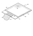
図1は、第1実施形態における液晶表示装置100の概略の構成を示す斜視図である。液晶表示装置100は、アレイ基板101、対向基板107、及びアレイ基板101と対向基板107との間に保持された液晶層108(図3)を含む。アレイ基板101は、複数の画素102がマトリクス状に配列された表示領域103及び表示領域103の周辺に位置する周辺領域104を有する。周辺領域104には、表示領域103に対して外部からの信号を供給するFPC(フレキシブルプリント回路)基板105及び表示領域103に対して供給する駆動信号を生成する駆動用IC(集積回路)106が配置される。
FIG. 1 is a perspective view showing a schematic configuration of a liquid
なお、アレイ基板101及び対向基板107には、偏光フィルム(図示せず)が隣接して設けられていてもよい。また、アレイ基板101及び対向基板107のいずれか一方に隣接してバックライトが設けられていてもよい。
A polarizing film (not shown) may be provided adjacent to the
アレイ基板101は、複数の画素102に薄膜トランジスタ等のスイッチング素子を含み、アクティブマトリクス基板とも呼ばれる。各画素102は、スイッチング素子として薄膜トランジスタを用いた画素回路を有し、スイッチング素子のON/OFF動作を制御することにより、各画素102に対応する液晶層の配向制御を行う構成となっている。
The
FPC基板105及び駆動用IC106は、図1には図示されない接続端子に接続され、表示領域103に対して所定の信号を供給する。本実施形態では、図示しない外部装置からFPC基板105を介して供給された映像信号が駆動用IC106に入力される。駆動用IC106に入力された映像信号は、所定の信号処理が施された後、表示領域103に対して出力される。また、駆動用IC106は、表示領域103に配置された走査線、信号線(図示せず)に所定の信号を供給するための駆動信号を生成する。
The
図1では、表示領域103を構成する走査線及び信号線を駆動するために、駆動用IC106を設けた例を示しているが、別途、表示領域103の周囲に、薄膜トランジスタで形成されたゲートドライバ回路やソースドライバ回路を設けた構成とすることもできる。その場合、それらゲートドライバ回路やソースドライバ回路は、駆動用IC106から出力される駆動信号(スタートパルス等)によって駆動される。
FIG. 1 shows an example in which a driving
アレイ基板101と対向基板107との間には液晶層108(図3)が保持される。アレイ基板101、対向基板107及びそれらの間の液晶層108を含む構造体を液晶セルと呼ぶ場合がある。対向基板107は、例えば、樹脂材料で構成されるシール材を用いてアレイ基板101に接着される。
A liquid crystal layer 108 (FIG. 3) is held between the
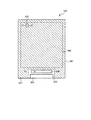
図2は、第1実施形態における液晶表示装置100の概略の構成を示す平面図である。ただし、図2では、図1に示したFPC基板105及び駆動用IC106の図示を省略している。図2に示されるように、FPC基板105が実装される部分には、FPC実装部205が設けられている。また、駆動用IC106が実装される部分には、IC実装部206が設けられている。FPC実装部205及びIC実装部206は、露出した複数の端子電極で構成される接続端子である。
FIG. 2 is a plan view showing a schematic configuration of the liquid
図2において、斜線のハッチングで示した領域201は、後述するアンダーコート膜12(図3)が設けられている領域である。また、斜線のハッチングが施されていない領域202は、後述するアンダーコート膜12が設けられていない領域である。ここでいう「アンダーコート膜」とは、支持基板と薄膜トランジスタとの間に設けられた無機絶縁膜を指す。本実施形態の液晶表示装置100は、IC実装部206の近傍だけアンダーコート膜12が設けられていない。
In FIG. 2, the
図3は、図2において、画素102をIII−IIIで示される一点鎖線で切断した断面図である。図3において、アレイ基板101は、支持基板としての樹脂基板11、アンダーコート膜12、TFT(薄膜トランジスタ)13、平坦化膜14、共通電極15、無機絶縁膜16、画素電極17、及び配向膜18を含む。勿論、これらに限らず、他の要素を含んでいても構わない。
FIG. 3 is a cross-sectional view of the
樹脂基板11は、透明な樹脂材料で構成された、可撓性を有する基板である。そのため、樹脂基板11を「第1可撓性基板」と呼ぶ場合がある。なお、本明細書中における「樹脂基板」とは、樹脂材料で構成された平板状の部材を指す。例えば、樹脂基板には、成型加工をしたシート状の樹脂材料で構成された部材(樹脂シート)や膜状の樹脂材料で構成された部材(樹脂膜)も含まれる。本実施形態では、可撓性を有する、透明なポリイミド基板を用いる。
The
なお、ここでいう「透明」とは、可視光に対して透光性を有することを意味するが、ヘーズ(曇り度)が10%以下(好ましくは5%以下、より好ましくは3%以下、最も好ましくは1%以下)であることが望ましい。ヘーズは、樹脂基板について、JIS K7361に準じたヘーズ測定器(例えば、日本電色工業社製の商品名「NDH−2000」)を用いて測定することができる。具体的には、全光線透過率Tt(%)と散乱光透過率Td(%)とを求め、これらの数値からヘーズ(Td/Tt×100(%))を算出することができる。なお、ヘーズ測定器としては、スガ試験機株式会社のヘーズメーターを用いることも可能である。 The term "transparent" as used herein means having transparency to visible light, but the haze (cloudiness) is 10% or less (preferably 5% or less, more preferably 3% or less). Most preferably, it is 1% or less). The haze can be measured with respect to the resin substrate using a haze measuring instrument according to JIS K7361 (for example, a trade name “NDH-2000” manufactured by Nippon Denshoku Kogyo Co., Ltd.). Specifically, the total light transmittance Tt (%) and the scattered light transmittance Td (%) can be obtained, and the haze (Td / Tt × 100 (%)) can be calculated from these numerical values. As the haze measuring instrument, a haze meter manufactured by Suga Test Instruments Co., Ltd. can also be used.
アンダーコート膜12は、酸化シリコン膜、窒化シリコン膜などの無機絶縁膜である。アンダーコート膜12は、樹脂基板11からの水分又はガスの侵入を防ぐバリア膜として機能する。そのため、アンダーコート膜12としては、バリア性の高い無機絶縁膜を用いることが多い。また、バリア性をより高めるため、アンダーコート膜12の膜厚は、100nm以上(好ましくは300nm以上、より好ましくは450nm以上)であることが望ましい。本実施形態では、アンダーコート膜12の膜厚を600nmとする。また、本明細書では、アンダーコート膜12を「第1絶縁膜」と呼ぶ場合がある。
The
TFT13は、画素102のON/OFF状態を制御するスイッチング素子として機能する。本実施形態では、TFT13として、いわゆるボトムゲート型TFTを用いる例を示している。具体的には、本実施形態のTFT13は、ゲート電極13a、ゲート絶縁膜13b、活性層13c、ドレイン電極13d、ソース電極13e、及び保護膜13fを含む。本実施形態では、ドレイン電極13d及びソース電極13eを、金属材料で構成する。なお、これらドレイン電極13d及びソース電極13eの機能は、キャリアの移動する向きに応じて入れ替わる場合がある。
The
ゲート電極13aは、モリブデン、チタン、タンタル等の金属材料で構成される。ゲート絶縁膜13bは、酸化シリコンを主成分とする無機材料で構成される。本実施形態では、ゲート絶縁膜13bの膜厚を120nmとするが、これに限られるものではない。
The
本実施形態において、TFT13の活性層13cは、酸化物半導体で構成されている。酸化物半導体としては、例えば透明アモルファス酸化物半導体(Transparent Amorphous Oxide Semiconductor:TAOS)を用いることができる。具体的には、インジウム、ガリウム、及び亜鉛の少なくとも1つを含む酸化物、例えば、酸化インジウムガリウム亜鉛(IGZO)、酸化インジウムガリウム(IGO)、インジウム亜鉛酸化物(IZO)、亜鉛スズ酸化物(ZnSnO)、亜鉛酸化物(ZnO)などを用いることができる。
In the present embodiment, the
本実施形態の場合、樹脂基板11の材料となる樹脂材料をガラス基板上に形成した状態でTFT13を形成するため、樹脂材料の耐熱性を考慮する必要がある。その点、酸化物半導体は、25℃から100℃程度の非常に低い温度で成膜することが可能であるため、樹脂材料を形成した後でも成膜することが可能である。なお、活性層13cとしては、樹脂材料の耐熱温度以内で成膜可能な半導体であれば如何なる材料を用いてもよく、例えばアモルファスシリコンを用いることも可能である。
In the case of this embodiment, since the
保護膜15fは、酸化シリコンで構成される無機絶縁膜であり、TFT13を、樹脂材料で構成される平坦化膜14から保護する役割を果たす。つまり、平坦化膜14が活性層13cに直接接触することを防ぐ機能を有する。
The protective film 15f is an inorganic insulating film made of silicon oxide, and serves to protect the
平坦化膜14は、樹脂材料で構成される有機絶縁膜である。平坦化膜14は、TFT13によって生じる起伏を平坦化する機能を有する。本実施形態では、平坦化膜14に使用する樹脂材料としてアクリル樹脂を用いるが、ポリイミド、ポリアミドといった他の樹脂材料を用いてもよい。
The flattening
共通電極15は、透明導電膜で構成される電極である。具体的には、共通電極15は、対向する画素電極17との間に横方向の電界を形成するための電極である。透明導電膜としては、ITO(Indium Tin Oxide)、ZnO(Zinc Oxide)に代表される無機化合物を用いることができる。
The
無機絶縁膜16は、窒化シリコンで構成され、共通電極15及び平坦化膜14を覆うように設けられる。本実施形態において、無機絶縁膜16は、共通電極15と画素電極17とを電気的に絶縁するとともに、共通電極15と画素電極17とで構成される保持容量の誘電体としても機能する。
The inorganic insulating
画素電極17は、透明導電膜で構成される電極である。透明導電膜としては、ITO(Indium Tin Oxide)、ZnO(Zinc Oxide)に代表される無機化合物を用いることができる。画素電極17は、平坦化膜14に設けられたコンタクトホールを介してTFT13のドレイン電極13dと電気的に接続される。これにより、TFT13を介して画素電極17の電位を制御することが可能となり、共通電極15と画素電極17との間に所望の電圧を与えることができる。
The
このようにして共通電極15と画素電極17との間に電界が形成され、その電界により液晶層108の液晶分子の配向が制御される。なお、配向膜18は、公知の配向膜を用いることができるが、省略することも可能である。
In this way, an electric field is formed between the
前述のように、本実施形態では、画素電極17と共通電極15との間に横方向の電界(横電界)を形成する。このように横電界を利用する表示装置をIPS(In−plain Swtching)方式と呼ぶ。また、IPS方式において、本実施形態のように共通電極15と画素電極17を重ねて配置する場合の横電界(この場合は、フリンジ電界ともいう。)を利用する方式を、FFS(Fringe Field Switching)方式と呼ぶ。
As described above, in the present embodiment, a lateral electric field (lateral electric field) is formed between the
ただし、液晶表示方式は、他の如何なる液晶表示方式を用いてもよい。例えば、同一層に設けられた画素電極と共通電極とを用いて形成した横電界を利用する方式を用いてもよい。また、アレイ基板側に設けられた画素電極と、対向基板側に設けられた共通電極との間に縦電界を形成し、その縦電界で液晶の配向を制御するVA(Vertical Alignment)方式を用いてもよい。 However, as the liquid crystal display method, any other liquid crystal display method may be used. For example, a method using a lateral electric field formed by using a pixel electrode provided on the same layer and a common electrode may be used. Further, a VA (Vertical Alignment) method is used in which a vertical electric field is formed between a pixel electrode provided on the array substrate side and a common electrode provided on the opposite substrate side, and the orientation of the liquid crystal display is controlled by the vertical electric field. You may.
本実施形態の液晶表示装置100は、以上説明した構成を含むアレイ基板101と向かい合わせに配置された対向基板107を含む。本実施形態では、対向基板107は、可撓性を有する樹脂基板20、遮光膜21、カラーフィルタ22、オーバーコート膜23及び配向膜24を含む。なお、配向膜24は、公知の配向膜を用いることができるが、省略することも可能である。また、本明細書では、樹脂基板20を「第2可撓性基板」と呼ぶ場合がある。
The liquid
樹脂基板20としては、樹脂基板11と同様に、透光性を有する樹脂材料で構成された基板を用いることができる。勿論、これに限らず、樹脂基板11と樹脂基板20とを異なる材料で構成してもよい。
As the
遮光膜21は、例えば黒色顔料やカーボンを含有させた樹脂材料を用いて形成することが可能である。遮光膜21は、ブラックマトリクスとも呼ばれる。なお、遮光膜21は、遮光が目的で配置される部材であるため、遮光性を有する金属膜で代用することも可能である。しかし、反射光を抑えるためには、黒色顔料を含有させた樹脂材料を用いることが好ましい。
The light-shielding
カラーフィルタ22は、各画素の透光領域(バックライトからの光が透過する領域)に配置される。カラーフィルタ22は、例えば顔料を含有させた樹脂材料を用いて形成することが可能であり、顔料の種類に応じてR(赤)、G(緑)、B(青)、W(白)といった各色に対応するスペクトル光を透過させることができる。
The
図4は、図2において、IC実装部206の近傍をIV−IVで示される一点鎖線で切断した断面図である。図4において、樹脂基板11上には、アンダーコート膜12、金属膜31、無機絶縁膜32、端子電極33、平坦化膜14が設けられている。端子電極33は、平面視において複数並べて配置され、全体として接続端子を構成している。つまり、複数の端子電極33によって、IC実装部206における接続端子が構成されている。また、金属膜31は、平面視において、隣り合う端子電極33の間に配置される。
FIG. 4 is a cross-sectional view of the vicinity of the
IC実装部206の端子電極33には、異方性導電膜34により駆動用IC106のバンプ106a及び106bが接続される。異方性導電膜34は、バインダとしての樹脂層34a及び導電性粒子34bを含む。図4に示されるように、端子電極33と駆動用IC106の各バンプ106a及び106bとは、樹脂層34aに保持された導電性粒子34bによって電気的に接続される。
なお、金属膜31は、図3に示したゲート電極13aと同一の膜を加工して得た要素である。すなわち、金属膜31及びゲート電極13aは、同一の金属配線層(以下「第1金属配線層」という。)と言える。同様に、端子電極33は、図3に示したドレイン電極13d及びソース電極13eと同一の膜を加工して得た要素である。すなわち、端子電極33、ドレイン電極13d及びソース電極13eは、同一の金属配線層(以下「第2金属配線層」という。)と言える。
The
本明細書では、端子電極33を第2金属配線層の第1部分と呼び、ドレイン電極13d及びソース電極13eを第2金属配線層の第2部分と呼んで区別する場合がある。ここで「第1部分」とは、接続端子の要素として機能する部分を指し、「第2部分」とは薄膜トランジスタの要素として機能する部分を指す。
In the present specification, the
図4に示されるように、IC実装部206を含む領域においては、樹脂基板11上にアンダーコート膜12が存在しない。つまり、本実施形態では、周辺領域104において、IC実装部206の近傍だけ局所的にアンダーコート膜12が除去されている。本実施形態では、接続端子として機能する端子電極33と駆動用IC106(厳密には、バンプ106a及び106b)との間に導電性粒子34bが位置する。すなわち、駆動用IC106を接続端子に対して圧着する際、端子電極33にはバンプ106a及び106b並びに導電性粒子34bを介して大きな力が加わる。しかしながら、端子電極33と樹脂基板11との間にはアンダーコート膜12が存在しないため、アンダーコート膜12にクラックが発生して樹脂基板11にダメージが入るという問題は解消される。
As shown in FIG. 4, the
前述のとおり、アンダーコート膜12は、樹脂基板11からの水分やガスの侵入を防ぐバリア膜として機能する。これは、表示領域103において樹脂基板11の上に配置されたTFT13を、樹脂基板11からの水分やガスから保護するためである。逆に言えば、TFT13が配置されないFPC実装部205及びIC実装部206に関しては、アンダーコート膜12が無くても問題はないと言える。そこで、本実施形態では、少なくともIC実装部206には無機絶縁膜で構成されるアンダーコート膜12を設けない構成とすることにより、前述のIC実装部206において無機絶縁膜にクラックが発生するという不具合を防ぐ構成となっている。
As described above, the
なお、図4に示した構造の場合、端子電極33と樹脂基板11との間に無機絶縁膜32(表示領域103ではゲート絶縁膜13bとして機能する。)が存在する。しかしながら、本実施形態では、ゲート絶縁膜13bの膜厚(すなわち、無機絶縁膜32の膜厚)が、アンダーコート膜12の膜厚に比べて十分に薄いため、クラック等の問題は発生しない。
In the case of the structure shown in FIG. 4, an inorganic insulating film 32 (functions as a
また、本実施形態では、平面視において、隣り合う端子電極33の間に金属膜31を配置する構成としたが、金属膜31を省略することも可能である。ただし、本実施形態では、IC実装部206にアンダーコート膜12を設けない構成とするため、金属膜31を設けた方がIC実装部206の強度を確保する上では好ましい。また、本実施形態では、端子電極33として第2金属配線層を用いた例を示したが、第1金属配線層を用いて端子電極33を構成してもよい。
Further, in the present embodiment, the
(第2実施形態)
図5を参照して、第2実施形態の液晶表示装置100aについて説明する。第2実施形態の液晶表示装置100aと第1実施形態の液晶表示装置100とが異なる点は、IC実装部206において、一部にアンダーコート膜12を残した点である。したがって、本実施形態では、第1実施形態と相違する点に着目して説明を行い、第1実施形態の液晶表示装置100と同一の部分については、同一の符号を付して説明を省略する場合がある。
(Second Embodiment)
The liquid
図5は、第2実施形態における液晶表示装置100aのIC実装部206の近傍を切断した断面図である。図5に示される液晶表示装置100aでは、金属膜31の下にアンダーコート膜12が存在する。すなわち、樹脂基板11と金属膜31との間に、アンダーコート膜12が残してある。換言すれば、平面視において、端子電極33の下にはアンダーコート膜12が存在せず、隣り合う端子電極33の間には、アンダーコート膜12が存在している。
FIG. 5 is a cross-sectional view taken along the vicinity of the
本実施形態の構造とした場合、第1実施形態に比べて、よりIC実装部206の強度を向上させることができる。
When the structure of the present embodiment is adopted, the strength of the
(第3実施形態)
図6を参照して、第3実施形態の液晶表示装置100bについて説明する。第3実施形態の液晶表示装置100bと第1実施形態の液晶表示装置100とが異なる点は、アンダーコート膜12の上に緩和層として有機絶縁膜を設けた点である。したがって、本実施形態では、第1実施形態と相違する点に着目して説明を行い、第1実施形態の液晶表示装置100と同一の部分については、同一の符号を付して説明を省略する場合がある。
(Third Embodiment)
The liquid
図6は、第3実施形態における液晶表示装置100bのIC実装部206の近傍を切断した断面図である。本実施形態の液晶表示装置100bでは、アンダーコート膜12の上に有機絶縁膜36を設けている。すなわち、IC実装部206において、端子電極33とアンダーコート膜12との間に、有機絶縁膜36が存在する。有機絶縁膜36としては、ポリイミド、アクリル等の樹脂材料で構成される膜を用いることができる。このとき、有機絶縁膜36の膜厚は、1μm以上5μm以下(好ましくは、1μm以上2μm以下)とすることが望ましい。
FIG. 6 is a cross-sectional view cut out in the vicinity of the
本実施形態の構造とした場合、端子電極33とアンダーコート膜12との間に、アンダーコート膜12よりも柔らかい(弾性率が低い)有機絶縁膜36を設けているため、有機絶縁膜36が緩衝層として機能する。つまり、導電性粒子34bによって端子電極33に大きな力が加わったとしても、有機絶縁膜36によって力が分散されるため、アンダーコート膜12には大きな力が加わらない。したがって、アンダーコート膜12にクラック等が発生することを防ぐことができる。
In the structure of the present embodiment, since the organic insulating
なお、図6では、アンダーコート膜12と無機絶縁膜32との間に有機絶縁膜36を設けた例を示しているが、これに限られるものではない。つまり、端子電極33とアンダーコート膜12との間であれば、どの層に有機絶縁膜を設けても本実施形態の効果を得ることができる。
Note that FIG. 6 shows an example in which the organic insulating
図7は、第3実施形態における液晶表示装置100cのIC実装部206の近傍を切断した断面図である。図7では、無機絶縁膜32と端子電極33との間に有機絶縁膜37が設けられている。この場合においても、有機絶縁膜37は、端子電極33から受ける力を分散させる緩衝層として機能する。
FIG. 7 is a cross-sectional view taken along the vicinity of the
なお、図6では、アンダーコート膜12に接して有機絶縁膜36を設ける構成について説明したが、この場合、有機絶縁膜36として、色材(特に、顔料又は染料)を含む樹脂材料を用いることも可能である。例えば、有機絶縁膜36に対して赤色顔料、青色顔料又は緑色顔料を添加することにより、表示領域103において、有機絶縁膜36をカラーフィルタとして利用することが可能である。また、例えば、有機絶縁膜36に対して黒色顔料を添加することにより、表示領域103又は周辺領域104において、遮光膜として利用することが可能である。さらに、有機絶縁膜36は、表示領域103において、カラーフィルタや遮光膜を平坦化するオーバーコート膜として利用することも可能である。
In addition, in FIG. 6, the configuration in which the organic insulating
また、液晶表示装置100b又は液晶表示装置100cを折り曲げる際の湾曲部分において中立面の制御や湾曲部分のほどを目的として設けられた有機絶縁膜を、図6に示した有機絶縁膜36や図7に示した有機絶縁膜37として利用することも可能である。
Further, the organic insulating
なお、「中立面」とは、複数の膜を積層した構造体を湾曲させた場合に、各膜に発生する圧縮応力と引張応力とが逆転する面をいう。つまり、湾曲部分の凹面側には圧縮応力が働き、凸面側には引っ張り応力が働くが、これらの応力が釣り合う面を中立面という。中立面は、湾曲部分の積層構造を変化させることにより位置を制御することが可能である。 The "neutral surface" refers to a surface in which the compressive stress and the tensile stress generated in each film are reversed when the structure in which a plurality of films are laminated is curved. That is, compressive stress acts on the concave side of the curved portion and tensile stress acts on the convex side, and the surface in which these stresses are balanced is called a neutral surface. The position of the neutral surface can be controlled by changing the laminated structure of the curved portion.
(第4実施形態)
図8を参照して、第4実施形態の液晶表示装置100dについて説明する。第4実施形態の液晶表示装置100dと第1実施形態の液晶表示装置100とが異なる点は、平坦化膜14の上に端子電極39を設けた点である。したがって、本実施形態では、第1実施形態と相違する点に着目して説明を行い、第1実施形態の液晶表示装置100と同一の部分については、同一の符号を付して説明を省略する場合がある。
(Fourth Embodiment)
The liquid
図8は、第4実施形態における液晶表示装置100dのIC実装部206の近傍を切断した断面図である。本実施形態の液晶表示装置100dでは、IC実装部206においても平坦化膜14を残し、平坦化膜14の上に端子電極39を設けた構成としている。このとき、端子電極39は、図3に示した共通電極15と同時に形成される。すなわち、本実施形態において、端子電極39は、表示領域103における共通電極15と同一の層構造及び同一の材料で構成される。
FIG. 8 is a cross-sectional view taken along the vicinity of the
本実施形態では、端子電極39の下に樹脂材料で構成される平坦化膜14が存在するため、平坦化膜14が緩衝層として機能する。その結果、端子電極39に対して導電性粒子34bから力が加わっても、アンダーコート膜12にクラックが生じることを防ぐことができる。
In the present embodiment, since the flattening
(第5実施形態)
図9を参照して、第5実施形態の液晶表示装置100eについて説明する。第5実施形態の液晶表示装置100eと第1実施形態の液晶表示装置100とが異なる点は、接続端子の構造が積層構造となっている点である。したがって、本実施形態では、第1実施形態と相違する点に着目して説明を行い、第1実施形態の液晶表示装置100と同一の部分については、同一の符号を付して説明を省略する場合がある。
(Fifth Embodiment)
The liquid
図9は、第5実施形態における液晶表示装置100eのIC実装部206の近傍を切断した断面図である。図9において、補助電極41は、端子電極33の下方に配置される。補助電極41と端子電極33は、無機絶縁膜32に設けられた開口部を介して電気的に接続される。つまり、補助電極41及び端子電極33は、いずれも接続端子の要素として機能する。なお、無機絶縁膜32は、ゲート絶縁膜13bと同一プロセスで形成された絶縁膜である。
FIG. 9 is a cross-sectional view taken along the vicinity of the
このとき、補助電極41は、金属膜31と同様に、図3に示したゲート電極13aと同一の膜を加工して得た要素である。すなわち、補助電極41及びゲート電極13aは、互いに同一の層構造及び同一の材料で構成される第1金属配線層である。本明細書では、補助電極41を第1金属配線層の第1部分と呼び、ゲート電極13aを第1金属配線層の第2部分と呼んで区別する場合がある。
At this time, the
本実施形態によれば、補助電極41と端子電極33の積層構造が複数並んで接続端子を構成するため、接続端子全体の抵抗を下げることができる。また、補助電極41及び端子電極33のいずれかが断線しても接続端子としての機能を維持することが可能である。
According to the present embodiment, since a plurality of laminated structures of the
(第6実施形態)
図10及び図11を参照して、第6実施形態の液晶表示装置100fについて説明する。第6実施形態の液晶表示装置100fと第1実施形態の液晶表示装置100とが異なる点は、接続端子の構造が積層構造となっている点である。したがって、本実施形態では、第1実施形態と相違する点に着目して説明を行い、第1実施形態の液晶表示装置100と同一の部分については、同一の符号を付して説明を省略する場合がある。
(Sixth Embodiment)
The liquid
図10は、第6実施形態における液晶表示装置100fの画素を切断した断面図である。図11は、第6実施形態における液晶表示装置100fのIC実装部206の近傍を切断した断面図である。
FIG. 10 is a cross-sectional view of the liquid
図10に示されるように、本実施形態の液晶表示装置100fでは、TFT43が2つのゲート電極を有するデュアルゲート型TFTで構成されている。具体的には、本実施形態のTFT43は、第1ゲート電極43a、第1ゲート絶縁膜43b、活性層43c、第2ゲート絶縁膜43d、第2ゲート電極43e、無機絶縁膜43f、ドレイン電極43g、及びソース電極43hを含む。なお、図示されないが、第1ゲート電極43aと第2ゲート電極43eは、それぞれ異なるゲート電圧が印加されてもよいし、同じゲート電圧が印加されてもよい。同じゲート電圧を印加する場合、第1ゲート電極43aと第2ゲート電極43eとを電気的に接続すればよい。
As shown in FIG. 10, in the liquid
第1ゲート電極43aは、第1実施形態において図3に示したゲート電極13aと同じ金属材料で構成することができる。第2ゲート電極43eは、第1ゲート電極43aと同じ金属材料で構成してもよいし、異なる金属材料で構成してもよい。本実施形態では、同じ金属材料を用いて第1ゲート電極43a及び第2ゲート電極43eを構成する。
The
活性層43cは、第1実施形態において図3に示した活性層13cと同じ半導体で構成することができる。本実施形態では、TFT43の活性層43cとして、酸化物半導体を用いるが、これに限られるものではない。
The
本実施形態では、活性層43cに対して第1ゲート電極43a及び第2ゲート電極43eの両方が作用し、TFT43をスイッチング素子として機能させることができる構成となっている。さらに、本実施形態では、図11に示されるように、第1ゲート電極43a及び第2ゲート電極43eのそれぞれと同時に形成された金属配線層を接続端子の要素として利用する。
In the present embodiment, both the
図11において、第1補助電極45及び第2補助電極48は、端子電極50の下方に配置される。第1補助電極45と第2補助電極48は、無機絶縁膜46及び47に設けられた開口部を介して電気的に接続される。また、第2補助電極48と端子電極50は、無機絶縁膜49に設けられた開口部を介して電気的に接続される。つまり、第1補助電極45、第2補助電極48及び端子電極50は、いずれも接続端子の要素として機能する。なお、無機絶縁膜46、47及び49は、それぞれ第1ゲート絶縁膜43b、第2ゲート絶縁膜43d及び無機絶縁膜43fと同一プロセスで形成された絶縁膜である。
In FIG. 11, the first
このとき、第1補助電極45は、金属膜31と同様に、図10に示した第1ゲート電極
43aと同一の膜を加工して得た要素である。すなわち、第1補助電極45及び第1ゲート電極43aは、互いに同一の層構造及び同一の材料で構成される第1金属配線層である。本明細書では、第1補助電極45を第1金属配線層の第1部分と呼び、第1ゲート電極43aを第1金属配線層の第2部分と呼んで区別する場合がある。
At this time, the first
また、第2補助電極48は、図10に示した第2ゲート電極43eと同一の膜を加工して得た要素である。すなわち、第2補助電極48及び第2ゲート電極43eは、互いに同一の層構造及び同一の材料で構成される第3金属配線層である。本明細書では、第2補助電極48を第3金属配線層の第1部分と呼び、第2ゲート電極43eを第3金属配線層の第2部分と呼んで区別する場合がある。
Further, the second
本実施形態によれば、第1補助電極45、第2補助電極48及び端子電極50で構成される積層構造が複数並んで接続端子を構成するため、接続端子全体の抵抗を下げることができる。また、第1補助電極45、第2補助電極48及び端子電極50のいずれかが断線しても接続端子としての機能を維持することが可能である。
According to the present embodiment, since a plurality of laminated structures composed of the first
本発明の実施形態として説明した表示装置を基にして、当業者が適宜構成要素の追加、削除もしくは設計変更を行ったもの、又は、工程の追加、省略もしくは条件変更を行ったものも、本発明の要旨を備えている限り、本発明の範囲に含まれる。また、上述した各実施形態は、技術的矛盾の生じない範囲において、相互に組み合わせることが可能である。 Based on the display device described as the embodiment of the present invention, those skilled in the art have added, deleted or changed the design as appropriate, or added, omitted or changed the conditions of the process. As long as it has the gist of the invention, it is included in the scope of the present invention. Further, the above-described embodiments can be combined with each other as long as technical inconsistencies do not occur.
また、上述した実施形態の態様によりもたらされる作用効果とは異なる他の作用効果であっても、本明細書の記載から明らかなもの、又は、当業者において容易に予測し得るものについては、当然に本発明によりもたらされるものと解される。 In addition, even if the action / effect is different from the action / effect brought about by the above-described embodiment, those that are clear from the description of the present specification or those that can be easily predicted by those skilled in the art are of course. Is understood to be brought about by the present invention.
11…樹脂基板、12…アンダーコート膜、13…TFT、13a…ゲート電極、13b…ゲート絶縁膜、13c…活性層、13d…ドレイン電極、13e…ソース電極、13f…保護膜、14…平坦化膜、15…共通電極、15f…保護膜、16…無機絶縁膜、17…画素電極、18…配向膜、20…樹脂基板、21…遮光膜、22…カラーフィルタ、23…オーバーコート膜、24…配向膜、31…金属膜、32…無機絶縁膜、33…端子電極、34…異方性導電膜、34a…樹脂層、34b…導電性粒子、36、37…有機絶縁膜、39…端子電極、41…補助電極、43…TFT、43a…第1ゲート電極、43b…第1ゲート絶縁膜、43c…活性層、43d…第2ゲート絶縁膜、43e…第2ゲート電極、43f…無機絶縁膜、43g…ドレイン電極、43h…ソース電極、45…第1補助電極、46、47…無機絶縁膜、48…第2補助電極、49…無機絶縁膜、50…端子電極、100、100a〜100f…液晶表示装置、101…アレイ基板、102…画素、103…表示領域、104…周辺領域、105…FPC基板、106…駆動用IC、106a、106b…バンプ、107…対向基板、108…液晶層、205…FPC実装部、206…IC実装部 11 ... Resin substrate, 12 ... Undercoat film, 13 ... TFT, 13a ... Gate electrode, 13b ... Gate insulating film, 13c ... Active layer, 13d ... Drain electrode, 13e ... Source electrode, 13f ... Protective film, 14 ... Flattening Film, 15 ... common electrode, 15f ... protective film, 16 ... inorganic insulating film, 17 ... pixel electrode, 18 ... alignment film, 20 ... resin substrate, 21 ... light-shielding film, 22 ... color filter, 23 ... overcoat film, 24 ... Alignment film, 31 ... Metal film, 32 ... Inorganic insulating film, 33 ... Terminal electrode, 34 ... Anisotropic conductive film, 34a ... Resin layer, 34b ... Conductive particles, 36, 37 ... Organic insulating film, 39 ... Terminal Electrodes, 41 ... Auxiliary electrodes, 43 ... TFTs, 43a ... First gate electrodes, 43b ... First gate insulating film, 43c ... Active layer, 43d ... Second gate insulating film, 43e ... Second gate electrodes, 43f ... Inorganic insulation Film, 43 g ... drain electrode, 43h ... source electrode, 45 ... first auxiliary electrode, 46, 47 ... inorganic insulating film, 48 ... second auxiliary electrode, 49 ... inorganic insulating film, 50 ... terminal electrode, 100, 100a to 100f ... LCD display device, 101 ... Array substrate, 102 ... Pixels, 103 ... Display area, 104 ... Peripheral area, 105 ... FPC substrate, 106 ... Drive IC, 106a, 106b ... Bump, 107 ... Opposite substrate, 108 ... Liquid crystal layer , 205 ... FPC mounting unit, 206 ... IC mounting unit
Claims (6)
前記周辺領域にあり、集積回路が接続される接続端子と、
前記第1基板に接する第1絶縁膜と、
前記第1絶縁膜に接する第2絶縁膜と、
複数の金属配線層と、
を備え、
前記複数の金属配線層は、前記第1絶縁膜と前記第2絶縁膜との間に位置する第1金属配線層と、前記第2絶縁膜上に位置する第2金属配線層と、を含み、
前記接続端子は、複数の端子電極を含み、前記第2金属配線層の第1部分で構成され、
前記第1領域において、前記第1金属配線層と前記第1基板との間には、前記第1絶縁膜があり、
前記周辺領域において、前記第1金属配線層と前記第1基板との間には、前記第1絶縁膜がなく、前記接続端子と前記第1基板との間には、前記第2絶縁膜があり、
前記第1金属配線層は、前記周辺領域において、前記第1基板と接しており、隣り合う前記端子電極の間に位置している、アクティブマトリクス基板。 A first substrate having a first region in which a plurality of transistors having semiconductors are arranged and a peripheral region located around the first region,
Connection terminals in the peripheral area to which integrated circuits are connected,
The first insulating film in contact with the first substrate and
The second insulating film in contact with the first insulating film and
With multiple metal wiring layers,
Equipped with
The plurality of metal wiring layers include a first metal wiring layer located between the first insulating film and the second insulating film, and a second metal wiring layer located on the second insulating film. ,
The connection terminal includes a plurality of terminal electrodes and is composed of a first portion of the second metal wiring layer.
In the first region, there is the first insulating film between the first metal wiring layer and the first substrate.
In the peripheral region, wherein between the first metal wiring layer and the first substrate, the first insulating film is rather name between the said connection terminal first substrate, the second insulating film There is
The first metal wiring layer is an active matrix substrate which is in contact with the first substrate in the peripheral region and is located between the adjacent terminal electrodes.
表示領域において、前記半導体は、前記第1金属配線層の第2部分と前記第3金属配線層の第2部分との間にあり、
前記接続端子は、前記第1金属配線層の第1部分及び前記第3金属配線層の第1部分で構成される、請求項1に記載のアクティブマトリクス基板。 The plurality of metal wiring layers further include a third metal wiring layer.
In the display region, the semiconductor is between the second portion of the first metal wiring layer and the second portion of the third metal wiring layer.
The connection terminal, the first composed of the first portion and a first portion of the third metal interconnect layer of the metal interconnection layer, an active matrix substrate according to claim 1.
前記第1金属配線層の第2部分及び前記第3金属配線層の第2部分には、ゲート電圧が印加される、請求項2に記載のアクティブマトリクス基板。 The semiconductor is an oxide semiconductor and is
The active matrix substrate according to claim 2 , wherein a gate voltage is applied to the second portion of the first metal wiring layer and the second portion of the third metal wiring layer.
Priority Applications (3)
| Application Number | Priority Date | Filing Date | Title |
|---|---|---|---|
| JP2017104518A JP6967371B2 (en) | 2017-05-26 | 2017-05-26 | Active matrix substrate |
| US15/960,873 US10437087B2 (en) | 2017-05-26 | 2018-04-24 | Display device |
| US16/550,396 US10634941B2 (en) | 2017-05-26 | 2019-08-26 | Display device |
Applications Claiming Priority (1)
| Application Number | Priority Date | Filing Date | Title |
|---|---|---|---|
| JP2017104518A JP6967371B2 (en) | 2017-05-26 | 2017-05-26 | Active matrix substrate |
Publications (3)
| Publication Number | Publication Date |
|---|---|
| JP2018200377A JP2018200377A (en) | 2018-12-20 |
| JP2018200377A5 JP2018200377A5 (en) | 2020-06-18 |
| JP6967371B2 true JP6967371B2 (en) | 2021-11-17 |
Family
ID=64401526
Family Applications (1)
| Application Number | Title | Priority Date | Filing Date |
|---|---|---|---|
| JP2017104518A Active JP6967371B2 (en) | 2017-05-26 | 2017-05-26 | Active matrix substrate |
Country Status (2)
| Country | Link |
|---|---|
| US (2) | US10437087B2 (en) |
| JP (1) | JP6967371B2 (en) |
Families Citing this family (10)
| Publication number | Priority date | Publication date | Assignee | Title |
|---|---|---|---|---|
| KR102506035B1 (en) * | 2017-12-27 | 2023-03-03 | 엘지디스플레이 주식회사 | Electroluminescent display device |
| US10955857B2 (en) * | 2018-10-02 | 2021-03-23 | Ford Global Technologies, Llc | Stationary camera localization |
| CN109698160B (en) * | 2018-12-27 | 2020-09-25 | 厦门天马微电子有限公司 | Array substrate, manufacturing method thereof, display panel and display device |
| US11217557B2 (en) | 2019-05-14 | 2022-01-04 | Innolux Corporation | Electronic device having conductive particle between pads |
| CN112071819B (en) * | 2019-06-11 | 2023-05-16 | 群创光电股份有限公司 | Electronic device |
| CN112445015A (en) * | 2019-09-04 | 2021-03-05 | 群创光电股份有限公司 | Electronic device and method for manufacturing the same |
| JP2021124574A (en) * | 2020-02-04 | 2021-08-30 | 株式会社ジャパンディスプレイ | Electronic apparatus and manufacturing method for the same |
| JP2022002276A (en) * | 2020-06-22 | 2022-01-06 | 株式会社ジャパンディスプレイ | Detector |
| JP2022018426A (en) | 2020-07-15 | 2022-01-27 | 株式会社ジャパンディスプレイ | Display device |
| TWI830563B (en) * | 2022-12-30 | 2024-01-21 | 友達光電股份有限公司 | Electronic apparatus |
Family Cites Families (11)
| Publication number | Priority date | Publication date | Assignee | Title |
|---|---|---|---|---|
| JP4244208B2 (en) * | 1999-04-30 | 2009-03-25 | 株式会社半導体エネルギー研究所 | Semiconductor device |
| EP1720149A3 (en) * | 2005-05-02 | 2007-06-27 | Semiconductor Energy Laboratory Co., Ltd. | Display device |
| US7863612B2 (en) * | 2006-07-21 | 2011-01-04 | Semiconductor Energy Laboratory Co., Ltd. | Display device and semiconductor device |
| WO2011021439A1 (en) * | 2009-08-21 | 2011-02-24 | シャープ株式会社 | Liquid crystal display device and method for manufacturing liquid crystal display device |
| KR101873448B1 (en) * | 2011-07-15 | 2018-07-03 | 삼성디스플레이 주식회사 | Organinc light emitting display device and manufacturing method for the same |
| JP6124668B2 (en) * | 2013-04-26 | 2017-05-10 | 三菱電機株式会社 | Thin film transistor substrate and manufacturing method thereof |
| KR102066087B1 (en) * | 2013-05-28 | 2020-01-15 | 엘지디스플레이 주식회사 | Flexible display device and manufacturing method of the same |
| US9472507B2 (en) * | 2013-06-17 | 2016-10-18 | Samsung Display Co., Ltd. | Array substrate and organic light-emitting display including the same |
| JP2015007699A (en) | 2013-06-25 | 2015-01-15 | 三菱電機株式会社 | Liquid crystal display device and method for manufacturing the same |
| JP2016080723A (en) * | 2014-10-09 | 2016-05-16 | 株式会社ジャパンディスプレイ | Display device |
| JP6486291B2 (en) * | 2016-02-24 | 2019-03-20 | 株式会社ジャパンディスプレイ | Display device manufacturing method and display device |
-
2017
- 2017-05-26 JP JP2017104518A patent/JP6967371B2/en active Active
-
2018
- 2018-04-24 US US15/960,873 patent/US10437087B2/en active Active
-
2019
- 2019-08-26 US US16/550,396 patent/US10634941B2/en active Active
Also Published As
| Publication number | Publication date |
|---|---|
| US20190377216A1 (en) | 2019-12-12 |
| US10437087B2 (en) | 2019-10-08 |
| US20180341143A1 (en) | 2018-11-29 |
| US10634941B2 (en) | 2020-04-28 |
| JP2018200377A (en) | 2018-12-20 |
Similar Documents
| Publication | Publication Date | Title |
|---|---|---|
| JP6967371B2 (en) | Active matrix substrate | |
| US9905626B2 (en) | Array substrate, display panel and display apparatus | |
| US10698545B2 (en) | Display device with position input function | |
| US9146430B2 (en) | Pixel structure and liquid crystal display panel having the same | |
| US8576365B2 (en) | Display panel | |
| US9865621B2 (en) | Display device | |
| US10977974B2 (en) | Display device having an inspection circuit located between the edge of a counter substrate and a selector circuit | |
| US8143622B2 (en) | Display panel | |
| US20220163859A1 (en) | Display device and touch sensor | |
| US10921667B2 (en) | Display device | |
| KR102218049B1 (en) | Display device | |
| US11809049B2 (en) | Display device | |
| US10914995B2 (en) | Liquid crystal display panel | |
| US11754893B2 (en) | Display device | |
| US11385513B2 (en) | Liquid crystal display device and liquid crystal display device manufacturing method | |
| US10962853B1 (en) | Display substrate and display device | |
| JP4867807B2 (en) | Electro-optical device and electronic apparatus | |
| US10942406B2 (en) | Thin film transistor substrate and display panel | |
| US11609463B2 (en) | Display device | |
| US20220283455A1 (en) | Display device | |
| WO2021251323A1 (en) | Array substrate and display device | |
| JP2017129615A (en) | Display device |
Legal Events
| Date | Code | Title | Description |
|---|---|---|---|
| A521 | Request for written amendment filed |
Free format text: JAPANESE INTERMEDIATE CODE: A523 Effective date: 20200420 |
|
| A621 | Written request for application examination |
Free format text: JAPANESE INTERMEDIATE CODE: A621 Effective date: 20200420 |
|
| A977 | Report on retrieval |
Free format text: JAPANESE INTERMEDIATE CODE: A971007 Effective date: 20210315 |
|
| A131 | Notification of reasons for refusal |
Free format text: JAPANESE INTERMEDIATE CODE: A131 Effective date: 20210406 |
|
| A521 | Request for written amendment filed |
Free format text: JAPANESE INTERMEDIATE CODE: A523 Effective date: 20210513 |
|
| TRDD | Decision of grant or rejection written | ||
| A01 | Written decision to grant a patent or to grant a registration (utility model) |
Free format text: JAPANESE INTERMEDIATE CODE: A01 Effective date: 20211019 |
|
| A61 | First payment of annual fees (during grant procedure) |
Free format text: JAPANESE INTERMEDIATE CODE: A61 Effective date: 20211025 |
|
| R150 | Certificate of patent or registration of utility model |
Ref document number: 6967371 Country of ref document: JP Free format text: JAPANESE INTERMEDIATE CODE: R150 |