JP6961349B2 - Information processing device with non-volatile storage device, control method - Google Patents
Information processing device with non-volatile storage device, control method Download PDFInfo
- Publication number
- JP6961349B2 JP6961349B2 JP2017010752A JP2017010752A JP6961349B2 JP 6961349 B2 JP6961349 B2 JP 6961349B2 JP 2017010752 A JP2017010752 A JP 2017010752A JP 2017010752 A JP2017010752 A JP 2017010752A JP 6961349 B2 JP6961349 B2 JP 6961349B2
- Authority
- JP
- Japan
- Prior art keywords
- power
- volatile storage
- frequency
- information processing
- access
- Prior art date
- Legal status (The legal status is an assumption and is not a legal conclusion. Google has not performed a legal analysis and makes no representation as to the accuracy of the status listed.)
- Active
Links
Images


Classifications
-
- G—PHYSICS
- G06—COMPUTING; CALCULATING OR COUNTING
- G06F—ELECTRIC DIGITAL DATA PROCESSING
- G06F3/00—Input arrangements for transferring data to be processed into a form capable of being handled by the computer; Output arrangements for transferring data from processing unit to output unit, e.g. interface arrangements
- G06F3/12—Digital output to print unit, e.g. line printer, chain printer
- G06F3/1201—Dedicated interfaces to print systems
- G06F3/1202—Dedicated interfaces to print systems specifically adapted to achieve a particular effect
- G06F3/1218—Reducing or saving of used resources, e.g. avoiding waste of consumables or improving usage of hardware resources
- G06F3/122—Reducing or saving of used resources, e.g. avoiding waste of consumables or improving usage of hardware resources with regard to computing resources, e.g. memory, CPU
-
- G—PHYSICS
- G06—COMPUTING; CALCULATING OR COUNTING
- G06F—ELECTRIC DIGITAL DATA PROCESSING
- G06F3/00—Input arrangements for transferring data to be processed into a form capable of being handled by the computer; Output arrangements for transferring data from processing unit to output unit, e.g. interface arrangements
- G06F3/12—Digital output to print unit, e.g. line printer, chain printer
- G06F3/1201—Dedicated interfaces to print systems
- G06F3/1223—Dedicated interfaces to print systems specifically adapted to use a particular technique
- G06F3/1229—Printer resources management or printer maintenance, e.g. device status, power levels
-
- G—PHYSICS
- G06—COMPUTING; CALCULATING OR COUNTING
- G06F—ELECTRIC DIGITAL DATA PROCESSING
- G06F3/00—Input arrangements for transferring data to be processed into a form capable of being handled by the computer; Output arrangements for transferring data from processing unit to output unit, e.g. interface arrangements
- G06F3/12—Digital output to print unit, e.g. line printer, chain printer
- G06F3/1201—Dedicated interfaces to print systems
- G06F3/1278—Dedicated interfaces to print systems specifically adapted to adopt a particular infrastructure
- G06F3/1279—Controller construction, e.g. aspects of the interface hardware
-
- G—PHYSICS
- G06—COMPUTING; CALCULATING OR COUNTING
- G06F—ELECTRIC DIGITAL DATA PROCESSING
- G06F3/00—Input arrangements for transferring data to be processed into a form capable of being handled by the computer; Output arrangements for transferring data from processing unit to output unit, e.g. interface arrangements
- G06F3/12—Digital output to print unit, e.g. line printer, chain printer
- G06F3/1201—Dedicated interfaces to print systems
- G06F3/1278—Dedicated interfaces to print systems specifically adapted to adopt a particular infrastructure
- G06F3/1285—Remote printer device, e.g. being remote from client or server
- G06F3/1286—Remote printer device, e.g. being remote from client or server via local network
-
- H—ELECTRICITY
- H04—ELECTRIC COMMUNICATION TECHNIQUE
- H04N—PICTORIAL COMMUNICATION, e.g. TELEVISION
- H04N1/00—Scanning, transmission or reproduction of documents or the like, e.g. facsimile transmission; Details thereof
- H04N1/00885—Power supply means, e.g. arrangements for the control of power supply to the apparatus or components thereof
- H04N1/00888—Control thereof
- H04N1/00896—Control thereof using a low-power mode, e.g. standby
-
- H—ELECTRICITY
- H04—ELECTRIC COMMUNICATION TECHNIQUE
- H04N—PICTORIAL COMMUNICATION, e.g. TELEVISION
- H04N2201/00—Indexing scheme relating to scanning, transmission or reproduction of documents or the like, and to details thereof
- H04N2201/0077—Types of the still picture apparatus
- H04N2201/0094—Multifunctional device, i.e. a device capable of all of reading, reproducing, copying, facsimile transception, file transception
-
- Y—GENERAL TAGGING OF NEW TECHNOLOGICAL DEVELOPMENTS; GENERAL TAGGING OF CROSS-SECTIONAL TECHNOLOGIES SPANNING OVER SEVERAL SECTIONS OF THE IPC; TECHNICAL SUBJECTS COVERED BY FORMER USPC CROSS-REFERENCE ART COLLECTIONS [XRACs] AND DIGESTS
- Y02—TECHNOLOGIES OR APPLICATIONS FOR MITIGATION OR ADAPTATION AGAINST CLIMATE CHANGE
- Y02D—CLIMATE CHANGE MITIGATION TECHNOLOGIES IN INFORMATION AND COMMUNICATION TECHNOLOGIES [ICT], I.E. INFORMATION AND COMMUNICATION TECHNOLOGIES AIMING AT THE REDUCTION OF THEIR OWN ENERGY USE
- Y02D10/00—Energy efficient computing, e.g. low power processors, power management or thermal management
Landscapes
- Engineering & Computer Science (AREA)
- Theoretical Computer Science (AREA)
- Physics & Mathematics (AREA)
- Human Computer Interaction (AREA)
- General Engineering & Computer Science (AREA)
- General Physics & Mathematics (AREA)
- Mathematical Physics (AREA)
- Multimedia (AREA)
- Signal Processing (AREA)
- Memory System Of A Hierarchy Structure (AREA)
- Facsimiles In General (AREA)
- Power Sources (AREA)
Description
不揮発性記憶手段等を搭載可能な情報処理装置に関する。 The present invention relates to an information processing device capable of mounting a non-volatile storage means or the like.
不揮発性記憶媒体を有する情報処理装置は、ネットワーク送受信可能な状態で待機している時(ネットワーク待機時)や、節電状態で待機している時(節電待機時)がある。これらの場合、内部のアプリケーションやネットワーク先のサーバから、頻繁に不揮発記憶装置へのアクセスを受ける場合がある。 An information processing device having a non-volatile storage medium may be on standby in a network transmission / reception state (during network standby) or on standby in a power saving state (during power saving standby). In these cases, the non-volatile storage device may be frequently accessed from an internal application or a server at the network destination.
例えば、頻繁にスワップや、アプリケーションからのポーリングアクセスなどに伴う、HDD(不揮発記憶装置)アクセスがある場合を考える。アプリケーションが一定間隔でメモリにアクセスする場合、OSは、空きメモリを増やすため不定期にスワップを発生させる。この結果、HDDアクセス頻度が上がる。その結果、HDDの動作に影響を与える可能性が否定できない。 For example, consider the case where there is HDD (nonvolatile storage device) access frequently associated with swapping or polling access from an application. When the application accesses the memory at regular intervals, the OS generates swaps irregularly to increase the free memory. As a result, the HDD access frequency increases. As a result, the possibility of affecting the operation of the HDD cannot be denied.
また、例えば、スワップや、アプリケーションからのポーリングアクセスなどに伴う、SSD(不揮発記憶装置)への書き込みアクセスが頻繁にある場合を考える。SSDは、書き込み容量などに基づく書き込み回数の上限がある。書き込み回数がその上限に近づくと、SSDの動作に影響を与える可能性が否定できない。 Further, for example, consider a case where there is frequent write access to the SSD (nonvolatile storage device) due to swapping, polling access from an application, or the like. SSD has an upper limit of the number of writes based on the write capacity and the like. When the number of writes approaches the upper limit, it cannot be denied that the operation of the SSD may be affected.
特許文献1は、主記憶にローディングされたプログラムが、実行途中に補助記憶へスワップアウトされないように、スワップアウト禁止のためのシステムコールをOSへ発行する。OSはこれを受けて、この格納領域のスワップアウト禁止登録をする。
上述の背景技術においては、不揮発性記憶装置への頻繁なアクセスに基づく不揮発記憶装置の性能や物理的な機能への影響を軽減することが難しかった。
In the above-mentioned background technology, it has been difficult to reduce the influence on the performance and physical function of the non-volatile storage device based on frequent access to the non-volatile storage device.
本発明は、上述の問題点の少なくとも一つを鑑みてなされたものである。 The present invention has been made in view of at least one of the above-mentioned problems.
本発明の目的は、不揮発性記憶装置への頻繁なアクセスに基づく不揮発記憶装置の性能や物理的な機能への影響を軽減することである。 An object of the present invention is to reduce the influence on the performance and physical function of the non-volatile storage device based on frequent access to the non-volatile storage device.
本発明の別の目的は、頻繁なアクセスに基づく不揮発性記憶装置の性能や物理的な機能への影響を軽減するに際して、情報処理装置のユーザに対するレスポンスが低下しないようにすることである。 Another object of the present invention is to ensure that the response of the information processing device to the user is not reduced in reducing the influence on the performance and physical functions of the non-volatile storage device based on frequent access.
本発明の一つの側面は、実記憶領域からデータを退避させるための補助記憶領域が定義された不揮発性記憶手段と、情報処理装置が第一の電力状態から、第一の電力状態より消費電力が少ない第二の電力状態へ遷移することに基づいて、前記補助記憶領域へ前記実記憶領域からデータを退避させる頻度を所定の頻度以下に低減させる制御手段を備える情報処理装置であることを特徴とする。 One aspect of the present invention is a non-volatile storage means in which an auxiliary storage area for saving data from the real storage area is defined, and the information processing device consumes power from the first power state to the first power state. The information processing device is provided with a control means for reducing the frequency of saving data from the real storage area to the auxiliary storage area to a predetermined frequency or less based on the transition to the second power state in which the amount of data is small. And.
本発明の別の側面は、人感センサ手段と、補助記憶領域が定義された不揮発性記憶手段と、人感センサ手段の検知結果に基づいて、前記補助記憶領域へ前記実記憶領域からデータを退避させる頻度を所定の頻度以下に低減させる制御手段を備える情報処理装置であることを特徴とする。 Another aspect of the present invention is to transfer data from the real storage area to the auxiliary storage area based on the detection results of the motion sensor means, the non-volatile storage means in which the auxiliary storage area is defined, and the motion sensor means. The information processing device is provided with a control means for reducing the frequency of withdrawal to a predetermined frequency or less.
本発明の目的は、不揮発性記憶装置への頻繁なアクセスに基づく不揮発性記憶装置の性能や物理的な機能への影響を軽減することが出来る。 An object of the present invention is to reduce the influence on the performance and physical function of the non-volatile storage device based on frequent access to the non-volatile storage device.
以下、本発明を実施するための形態について、図面を用いて説明する。 Hereinafter, embodiments for carrying out the present invention will be described with reference to the drawings.
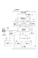
<システムの構成>
図1は、本実施形態を示す画像形成装置の構成を説明するブロック図である。本例は、プリント機能、スキャナ機能、データ通信機能等を備える複合機を例とする。画像形成装置(101)は、情報処理装置の一例である。
<System configuration>
FIG. 1 is a block diagram illustrating a configuration of an image forming apparatus showing the present embodiment. This example is an example of a multifunction device having a print function, a scanner function, a data communication function, and the like. The image forming apparatus (101) is an example of an information processing apparatus.
図1において、画像形成装置(101)は、LAN(108)を介してコンピュータ(109)よりジョブを受信可能に構成されている。なお、コンピュータの接続数は、1以上であってもよい。スキャナ装置(102)は、原稿から光学的に画像を読み取りデジタル画像に変換する。プリンタ装置(104)は、デジタル画像を用紙と呼ぶ紙デバイスに出力する。操作部(105)は、本装置に対する設定をユーザから受け付けたり、処理状態を表示したりするためのタッチパネルやハードキーを備えている。ハードディスク(HDDとも呼ぶ)(106)は、デジタル画像や制御プログラム等を記憶する。 In FIG. 1, the image forming apparatus (101) is configured to be able to receive a job from the computer (109) via the LAN (108). The number of computers connected may be 1 or more. The scanner device (102) optically reads an image from the original and converts it into a digital image. The printer device (104) outputs a digital image to a paper device called paper. The operation unit (105) is provided with a touch panel and hard keys for receiving settings for the present device from the user and displaying the processing status. The hard disk (also called HDD) (106) stores digital images, control programs, and the like.
FAX装置(107)は、電話回線等にデジタル画像を送受信する。コントローラ(103)は、スキャナ装置(102)、プリンタ装置(104)、操作部(105)、ハードディスク(106)、FAX装置(107)と接続され、各モジュールに指示を出す事で、画像形成装置(101)上でジョブを実行する。 The FAX device (107) transmits / receives digital images to / from a telephone line or the like. The controller (103) is connected to a scanner device (102), a printer device (104), an operation unit (105), a hard disk (106), and a fax device (107), and issues an instruction to each module to form an image forming device. (101) Execute the job on.
画像形成装置(101)は、LAN(108)経由でコンピュータ(109)からデジタル画像の入出力、ジョブの発行や機器の指示等も行なうことが可能である。スキャナ装置(102)は、原稿束を自動的に逐次入れ替えることが可能な原稿給紙ユニット(121)、原稿を光学スキャンしデジタル画像に変換する事が可能なスキャナユニット(122)から成る。また、変換された画像データはコントローラ(103)に送信される。 The image forming apparatus (101) can also input / output digital images, issue jobs, instruct equipment, and the like from the computer (109) via the LAN (108). The scanner device (102) includes a document feeding unit (121) capable of automatically sequentially replacing a bundle of documents, and a scanner unit (122) capable of optically scanning a document and converting it into a digital image. Further, the converted image data is transmitted to the controller (103).
プリンタ装置(104)は、紙束から一枚ずつ逐次給紙可能な給紙ユニット(142)、給紙した紙に画像データを印刷するためのマーキングユニット(141)、印刷後の紙を排紙するための排紙ユニット(143)から成る。フィニッシャ装置(150)は、画像形成装置(101)のプリンタ装置(104)の排紙ユニット(143)から出力された紙デバイスに対して、排紙、ソート、ステープル、パンチ、裁断、などの加工を施す。 The printer device (104) includes a paper feed unit (142) capable of sequentially feeding paper one by one from a bundle of paper, a marking unit (141) for printing image data on the paper fed, and discharging the printed paper. It consists of a paper ejection unit (143) for printing. The finisher device (150) processes the paper device output from the paper ejection unit (143) of the printer apparatus (104) of the image forming apparatus (101) to perform paper ejection, sorting, staples, punching, cutting, and the like. To give.
また、コントローラ(103)に接続された、電源スイッチ(110)を保持する。電源スイッチ(110)がオンになっていると、少なくとも後述する電源制御部(303)や操作部(105)、コントローラ(103)のメインボードの一部に対して給電されている。また、電源スイッチ(110)がオフになっても、即時に給電が停止するわけでなく、ソフトウェアやハードウェアの終了処理を待って、電源制御部(303)の一部など電源スイッチ(110)をONするために必要な部分以外の給電を停止する。 It also holds a power switch (110) connected to the controller (103). When the power switch (110) is turned on, power is supplied to at least a part of the main board of the power control unit (303), the operation unit (105), and the controller (103), which will be described later. Further, even if the power switch (110) is turned off, the power supply does not stop immediately, but the power switch (110) such as a part of the power control unit (303) waits for the software or hardware termination process. Stop the power supply other than the part necessary to turn on.
<システムの機能>
以下、画像形成装置(101)の実行可能なジョブ(機能)の一例を説明する。
<System functions>
Hereinafter, an example of an executable job (function) of the image forming apparatus (101) will be described.
〔複写機能〕
画像形成装置(101)は、スキャナ装置(102)から読み込んだ画像をハードディスク(106)に記録し、同時にプリンタ装置(104)を使用して印刷を行なう複写機能を備える。
[Copy function]
The image forming apparatus (101) has a copying function of recording an image read from the scanner apparatus (102) on the hard disk (106) and at the same time printing using the printer apparatus (104).
〔画像送信機能〕
画像形成装置(101)は、スキャナ装置(102)から読み込んだ画像を、LAN(108)を介してコンピュータ(109)に送信する画像送信機能を備える。
[Image transmission function]
The image forming apparatus (101) has an image transmission function of transmitting an image read from the scanner apparatus (102) to the computer (109) via the LAN (108).
〔画像保存機能〕
画像形成装置(101)は、スキャナ装置(102)から読み込んだ画像をハードディスク(106)やのフラッシュディスク(207、後述)に記録し、必要に応じて画像送信や画像印刷を行なう画像保存機能を備える。
[Image storage function]
The image forming apparatus (101) has an image saving function of recording an image read from the scanner apparatus (102) on a hard disk (106) or a flash disk (207, which will be described later), and transmitting or printing an image as needed. Be prepared.
〔画像印刷機能〕
画像形成装置(101)は、コンピュータ(109)から送信された、例えばページ記述言語を解析し、プリンタ装置(104)で印刷する画像印刷機能を備える。
[Image printing function]
The image forming apparatus (101) has an image printing function that analyzes, for example, a page description language transmitted from the computer (109) and prints it by the printer apparatus (104).
<操作部(105)の構成>
操作部(105)は、コントローラ(103)に接続され、LCDタッチパネルや、節電ボタン、コピーボタン、キャンセルボタン、リセットボタン、テンキー、ユーザモードキー、などで構成される。操作部(105)は、画像入出力システムを操作するためのユーザI/Fを提供する。また、操作部(105)と一体または別のユニットとして、赤外線などを用いて人などが近づいてきたことを検知する人感センサを設けることが想定できる。
<Structure of operation unit (105)>
The operation unit (105) is connected to the controller (103) and includes an LCD touch panel, a power saving button, a copy button, a cancel button, a reset button, a numeric keypad, a user mode key, and the like. The operation unit (105) provides a user I / F for operating the image input / output system. Further, it can be assumed that a motion sensor for detecting that a person or the like is approaching by using infrared rays or the like is provided as a unit integrated with or separate from the operation unit (105).
<コントローラ(103)のブロック図>
次に、図2を用いて、コントローラ(103)と周辺装置のブロック図を説明する。
<Block diagram of controller (103)>
Next, a block diagram of the controller (103) and peripheral devices will be described with reference to FIG.
コントローラ(103)はメインボード(200)と、サブボード(220)から構成される。 The controller (103) is composed of a main board (200) and a sub board (220).
メインボード(200)はいわゆる汎用的なCPUシステムである。ボード全体を制御するCPU(340)、ブートプログラムが含まれるブートロム(202)、CPUがワークメモリとして使用するメモリ(341)。外部バスとのブリッジ機能を持つバスコントローラ(204)、電源断された場合でも消えない不揮発性メモリ(205)がある。
さらに、コントローラ(103)は、ストレージ装置を制御するディスクコントローラ(206)と、半導体デバイスで構成されたフラッシュディスク(207)、USBを制御することが可能なUSBコントローラ(208)等から構成される。比較的小容量なストレージ装置であるフラッシュディスク(207)の一例は、ソリッドステートドライブ(SSD)等がある。
The main board (200) is a so-called general-purpose CPU system. A CPU (340) that controls the entire board, a bootrom (202) that includes a boot program, and a memory (341) that the CPU uses as a work memory. There is a bus controller (204) that has a bridging function with an external bus, and a non-volatile memory (205) that does not disappear even when the power is turned off.
Further, the controller (103) is composed of a disk controller (206) that controls a storage device, a flash disk (207) composed of semiconductor devices, a USB controller (208) that can control USB, and the like. .. An example of a flash disk (207), which is a storage device having a relatively small capacity, is a solid state drive (SSD) or the like.
メインボード(200)には外部に、USBメモリ(209)、操作部(105)、ハードディスク(106)等が接続される。 A USB memory (209), an operation unit (105), a hard disk (106), and the like are connected to the main board (200) to the outside.
また、CPU(340)は、各装置からの割り込みや各装置に対する電力供給を制御するCPLD(304)と接続されている。CPLDとは、Complex Programmable Logic Deviceの略である。さらに、ネットワークコントローラ(211)、リアルタイムクロック(RTC)(212)、FAX装置(107)、USBコントローラ(208)と接続されている。また、コントローラ外部に装置である、ソフトスイッチを持つ操作部(105)や、各種センサを持つスキャナ装置(102)、プリンタ装置(104)、フィニッシャ装置(150)、などと接続されている。 Further, the CPU (340) is connected to a CPLD (304) that controls interrupts from each device and power supply to each device. CPLD is an abbreviation for Complex Programmable Logic Device. Further, it is connected to a network controller (211), a real-time clock (RTC) (212), a fax machine (107), and a USB controller (208). Further, it is connected to an operation unit (105) having a soft switch, a scanner device (102) having various sensors, a printer device (104), a finisher device (150), and the like, which are devices outside the controller.
サブボード(220)は比較的小さな汎用CPUシステムと、画像処理ハードウェアから構成される。ボード全体を制御するCPU(221)、CPUがワークメモリとして使用するメモリ(223)、外部バスとのブリッジ機能を持つバスコントローラ(224)、電源断された場合でも消えない不揮発性メモリ(225)。 The sub board (220) is composed of a relatively small general-purpose CPU system and image processing hardware. A CPU that controls the entire board (221), a memory that the CPU uses as a work memory (223), a bus controller that has a bridging function with an external bus (224), and a non-volatile memory that does not disappear even when the power is turned off (225). ..
さらに、リアルタイムデジタル画像処理を行なう画像処理プロセッサ(227)とデバイスコントローラ(226)を有する。 Further, it has an image processing processor (227) and a device controller (226) that perform real-time digital image processing.
コントローラ(103)の外部に接続される、スキャナ装置(102)とプリンタ装置(104)は、デバイスコントローラ(226)を介して、デジタル画像データの受け渡しを行なう。プリンタ装置(104)から排紙した紙デバイスは、フィニッシャ装置(150)で加工する。FAX装置(107)はCPU(221)が直接制御を行なう。なお、本図はブロック図であり簡略化している。例えばCPU(340)、CPU(221)等にはチップセット、バスブリッジ、クロックジェネレータ等のCPU周辺ハードウェアが多数含まれている。 The scanner device (102) and the printer device (104), which are connected to the outside of the controller (103), transfer digital image data via the device controller (226). The paper device ejected from the printer device (104) is processed by the finisher device (150). The fax device (107) is directly controlled by the CPU (221). It should be noted that this figure is a block diagram and is simplified. For example, the CPU (340), the CPU (221), and the like include a large number of CPU peripheral hardware such as a chipset, a bus bridge, and a clock generator.
コントローラ(103)の動作について、紙デバイスによる画像複写を例に説明する。 The operation of the controller (103) will be described by taking image copying using a paper device as an example.
ユーザが操作部(105)から画像複写を指示すると、CPU(340)がCPU(221)を介してスキャナ装置(102)に画像読み取り命令を送る。スキャナ装置(102)は紙原稿を光学スキャンしデジタル画像データに変換してデバイスコントローラ(226)を介して画像処理プロセッサ(227)に入力する。画像処理プロセッサはCPU(221)を介してメモリ(223)にDMA転送を行いデジタル画像データの一時保存を行なう。 When the user instructs the image copying from the operation unit (105), the CPU (340) sends an image reading command to the scanner device (102) via the CPU (221). The scanner device (102) optically scans the paper document, converts it into digital image data, and inputs it to the image processing processor (227) via the device controller (226). The image processor performs DMA transfer to the memory (223) via the CPU (221) and temporarily stores the digital image data.
CPU(340)はデジタル画像データがメモリ(223)に一定量もしくは全て入ったことが確認できると、CPU(221)を介してプリンタ装置(104)に画像出力指示を出す。 When the CPU (340) can confirm that a certain amount or all of the digital image data is stored in the memory (223), the CPU (340) issues an image output instruction to the printer device (104) via the CPU (221).
CPU(221)は、画像処理プロセッサ(227)にメモリ(223)の画像データのアドレスを教える。メモリ(223)上の画像データは、プリンタ装置(104)からの同期信号に従って、画像処理プロセッサ(227)とデバイスコントローラ(226)を介してプリンタ装置(104)に送信される。 The CPU (221) teaches the image processor (227) the address of the image data in the memory (223). The image data on the memory (223) is transmitted to the printer device (104) via the image processor (227) and the device controller (226) according to the synchronization signal from the printer device (104).
プリンタ装置(104)は、紙デバイスにデジタル画像データを印刷する。 The printer device (104) prints digital image data on a paper device.
複数部印刷を行なう場合、CPU(340)がメモリ(223)の画像データをハードディスク(106)に対して保存を行う。2部目以降はスキャナ装置(102)から画像をもらわなくても、ハードディスク(106)やメモリ(223)から、プリンタ装置(104)に画像を送ることが可能である。なお、単数部印刷も同様に構成してもよい。 When printing a plurality of copies, the CPU (340) saves the image data of the memory (223) to the hard disk (106). From the second copy onward, it is possible to send an image from the hard disk (106) or the memory (223) to the printer device (104) without receiving the image from the scanner device (102). The printing of a single copy may be configured in the same manner.
<電源構成>
図3は、図1に示した画像形成装置(101)の電源構成を説明するブロック図である。以下、画像形成装置(101)における、コントローラ(103)とプリンタ装置(104)、電源制御部(303)、電源(301)の構成について、本発明に関わる部分を、図3を用いて説明する。図3において、電源制御部(303)には、第1の電源ラインである電源ラインJ(302)経由で常時電源が供給されている。ただし、微弱な電力消費にとどまるため、電源オフ時にはこの電源制御部(303)だけに通電され、電力制御が行われる。
<Power supply configuration>
FIG. 3 is a block diagram illustrating a power supply configuration of the image forming apparatus (101) shown in FIG. Hereinafter, the configurations of the controller (103), the printer device (104), the power supply control unit (303), and the power supply (301) in the image forming apparatus (101) will be described with reference to FIG. .. In FIG. 3, the power supply control unit (303) is constantly supplied with power via the power supply line J (302), which is the first power supply line. However, since the power consumption is very weak, only the power control unit (303) is energized when the power is turned off, and the power is controlled.
CPLD(結合プログラマブル論理回路)(304)は、あらかじめ下記に示す所望の動作を実行するようプログラムされている。すなわち、第1の電源制御信号であるIO信号V_ON(307)によって、リレースイッチ(308)が切り替わり電源(301)から第2の電源ラインである電源ラインV(309)経由で送られる、コントローラ(103)への給電が制御される。また、CPU(340)から通信により複数のタイマ値が設定され、タイマ起動時にはCPU(340)によって設定された動作を実行する。 The CPLD (coupling programmable logic circuit) (304) is pre-programmed to perform the desired operation shown below. That is, the relay switch (308) is switched by the IO signal V_ON (307), which is the first power supply control signal, and is sent from the power supply (301) via the power supply line V (309), which is the second power supply line. The power supply to 103) is controlled. Further, a plurality of timer values are set by communication from the CPU (340), and when the timer is started, the operation set by the CPU (340) is executed.
また、第2の電源制御信号であるIO信号P_ON(310)によって、リレースイッチ(311)が切り替わる。その結果、電源(301)から第3の電源ラインである電源ラインP(312)経由で送られる、プリンタ装置(104)のロジック系回路への給電が制御される。 Further, the relay switch (311) is switched by the IO signal P_ON (310) which is the second power supply control signal. As a result, the power supply to the logic system circuit of the printer device (104) transmitted from the power supply (301) via the power supply line P (312), which is the third power supply line, is controlled.
さらに、第2の電源制御信号のサブ信号であるIO信号Q_ON(313)によって、リレースイッチ(315)が切り替わる。その結果、電源(301)から第3の電源ラインのサブラインである電源ラインQ(316)経由で送られる、プリンタ装置(104)の負荷系装置への給電が制御される。前述の電源ラインQ(316)は、電源ラインP(312)のサブラインである必要はなく、電源(301)から引くことも可能であるが、本論から外れるため割愛する。また、リレースイッチ(315)は、CPLD(304)から制御しているが、CPU(320)などから制御することも可能であるが、本論から外れるため割愛する。 Further, the relay switch (315) is switched by the IO signal Q_ON (313) which is a sub signal of the second power supply control signal. As a result, the power supply to the load system device of the printer device (104) transmitted from the power supply (301) via the power supply line Q (316), which is a subline of the third power supply line, is controlled. The power supply line Q (316) described above does not have to be a subline of the power supply line P (312) and can be drawn from the power supply (301), but it is omitted because it deviates from the main subject. Further, although the relay switch (315) is controlled from the CPLD (304), it can also be controlled from the CPU (320) or the like, but it is omitted because it deviates from the main subject.
また、CPU(301)の指示によって、所定のIO信号を動作させる。動作させるIO信号のひとつはプリンタ装置(104)のCPU(320)へ接続されたDCON_LIVEWAKE信号(305)である。この信号がアサートされた状態でプリンタ装置(104)の電源が投入されると、プリンタ装置(104)は、可動部を制御したり電力を使ったりする特定の動作を行わず、静かに復帰する。その特定の動作には、例えば、モータ、ローラ、ポリゴンなどの回転動作や、ドラム(321、322、323、324)の温調やFAN(325)による排熱処理といった制御がある。スキャナ装置(102)は、プリンタ装置(104)と同様に、CPLD(304)から制御可能だが、内容が重複するため割愛する。すなわちスキャナ装置(102)についてもプリンタ装置(104)と同様の電源制御が行われる。 In addition, a predetermined IO signal is operated according to the instruction of the CPU (301). One of the IO signals to be operated is the DCON_LiveWAKE signal (305) connected to the CPU (320) of the printer device (104). When the power of the printer device (104) is turned on while this signal is asserted, the printer device (104) returns quietly without performing a specific operation such as controlling a moving part or using electric power. .. Specific operations include, for example, rotational operations of motors, rollers, polygons, etc., temperature control of drums (321, 322, 323, 324), and exhaust heat treatment by FAN (325). The scanner device (102) can be controlled from the CPLD (304) like the printer device (104), but it is omitted because the contents are duplicated. That is, the same power supply control as that of the printer device (104) is performed on the scanner device (102).
なお図3のようなブロックごとの給電は、たとえばリレースイッチ(308)を2系統で構成し、スリープ状態では、電源をオフするブロックにつながるリレースイッチのみをオフとし、他方をオンとしたままとすることなどで実現できる。シャットダウン状態では両方の系統のリレースイッチをオフにする。その場合には、電源制御信号は二値ではなく、通電状態に応じた多値制御信号となる。本例では特にそのような記載は省くが、スリープ状態やシャットダウン状態などを含む前述した各電力状態は、このような制御により電源供給が成される。 For the power supply for each block as shown in FIG. 3, for example, the relay switch (308) is configured by two systems, and in the sleep state, only the relay switch connected to the block that turns off the power is turned off, and the other is left on. It can be realized by doing. In the shutdown state, turn off the relay switches of both systems. In that case, the power supply control signal is not a binary value but a multi-valued control signal according to the energized state. In this example, such a description is omitted in particular, but each of the above-mentioned power states including the sleep state and the shutdown state is supplied with power by such control.
具体的には、CPLD(304)は、第3の電源制御信号であるIO信号N_ON(360)によって、リレースイッチ(361)を切り替え、電源(301)から第3の電源ラインである電源ラインN(362)経由で、NIC(350)への給電を制御する。コントローラ(103)の内、NIC(350)だけが、個別に給電されている。電源ラインN(362)は、他の非常夜電源と異なり、通常時だけでなく、スリープ時にも給電され、ネットワーク起床を可能にする。また、シャットダウン時はWake On LANなどの設定が有効でない限りは、給電しない。リレースイッチ(361)を経由した電源ラインN(362)は、オフ状態以外は常に給電状態で冗長になるため、以下では明示的に記載しない。 Specifically, the CPLD (304) switches the relay switch (361) by the IO signal N_ON (360) which is the third power supply control signal, and the power supply line N which is the third power supply line from the power supply (301). The power supply to the NIC (350) is controlled via (362). Of the controllers (103), only the NIC (350) is individually powered. Unlike other emergency night power supplies, the power supply line N (362) is supplied with power not only during normal times but also during sleep, enabling the network to wake up. Also, at shutdown, power is not supplied unless settings such as Wake On LAN are valid. The power supply line N (362) via the relay switch (361) is not explicitly described below because it is always redundant in the power supply state except in the off state.
さらに、第4の電源制御信号であるIO信号H_ON(370)によって、リレースイッチ(371)を切り替え、電源(301)から第4の電源ラインである電源ラインH(372)経由で、HDD(106)への給電を制御する。CPU(340)とHDD(106)やフラッシュディスク(207)間は、前述のブロック図の通り、ディスクコントローラ(206)を経由してデータをやり取りしている。フラッシュディスク(207)を、HDD(106)と入れ替えたり、HDD(106)と同時に給電することも可能である。HDD(106)およびフラッシュディスク(207)は、不揮発性記憶装置の一例である。 Further, the relay switch (371) is switched by the IO signal H_ON (370) which is the fourth power supply control signal, and the HDD (106) is switched from the power supply (301) via the power supply line H (372) which is the fourth power supply line. ) Is controlled. Data is exchanged between the CPU (340) and the HDD (106) or the flash disk (207) via the disk controller (206) as shown in the block diagram described above. The flash disk (207) can be replaced with the HDD (106), or power can be supplied at the same time as the HDD (106). The HDD (106) and the flash disk (207) are examples of non-volatile storage devices.
<電源制御部(303)の電源監視1:起動時の給電>
続いて、画像形成装置(101)の起動処理について、説明する。操作者が画像形成装置(101)を使用する場合は、電源スイッチ(110)をONにする。すると電源制御部(303)は電源ラインJ(302)より電源ONを検知し、電源スイッチ制御信号(307、310)によりリレースイッチ(308、311)をそれぞれオンにして電源(301)が電源電力を装置全体に供給する。電源制御部(303)は、システム全体に電源ON時に応じた電力供給、具体的にはコントローラ(103)、プリンタ装置(104)、スキャナ装置(102)に各DC電源供給径路を介して通電を行う。プリンタ装置(104)、スキャナ装置(102)は各々のCPUが電源ONによる初期化動作を開始する。
<Power supply monitoring of power supply control unit (303) 1: Power supply at startup>
Subsequently, the activation process of the image forming apparatus (101) will be described. When the operator uses the image forming apparatus (101), the power switch (110) is turned on. Then, the power supply control unit (303) detects that the power is turned on from the power supply line J (302), turns on the relay switches (308, 311) by the power switch control signals (307, 310), and the power supply (301) is the power supply power. Is supplied to the entire device. The power control unit (303) supplies power to the entire system according to when the power is turned on, specifically, energizes the controller (103), printer device (104), and scanner device (102) via each DC power supply route. conduct. Each CPU of the printer device (104) and the scanner device (102) starts an initialization operation when the power is turned on.
通電が行われると、コントローラ(103)のCPU(340)は、ハードウェア初期化を行う。ハードウェア初期化は、レジスタ初期化、割り込み初期化、カーネル起動時のデバイスドライバの登録、操作部(105)の初期化、などがある。次に、コントローラ(103)のCPU(340)は、ソフトウェア初期化を行う。ソフトウェア初期化は、各ライブラリの初期化ルーチンの呼び出し、プロセスやスレッドの起動、プリンタ装置(104)やスキャナ装置(102)とコミュニケーションを行うソフトウェアサービスの起動、操作部(105)の描画、などがある。最後に、スタンバイ状態へ移行する。スタンバイ状態は、通常状態と同義で用いる。 When the power is turned on, the CPU (340) of the controller (103) initializes the hardware. Hardware initialization includes register initialization, interrupt initialization, device driver registration at kernel startup, initialization of the operation unit (105), and the like. Next, the CPU (340) of the controller (103) initializes the software. Software initialization includes calling the initialization routine of each library, starting processes and threads, starting software services that communicate with the printer device (104) and scanner device (102), drawing the operation unit (105), and so on. be. Finally, it shifts to the standby state. The standby state is used synonymously with the normal state.
<電源制御部(303)の電源監視2:通常状態の給電>
続いて、画像形成装置(101)の、プリンタ装置(104)やスキャナ装置(102)を使っていない通常状態の給電について、説明する。通常状態は、すべてのユニットに給電されている状態だけでない。印刷していない時はプリンタ装置(104)に給電しない状態や、操作部(105)が点灯しておらず、ユーザが画像形成装置(101)の前にいないことが分かっている場合は、スキャナ装置(102)に対して給電しない状態などがある。
<Power supply monitoring of power supply control unit (303): Power supply in normal state>
Subsequently, the power supply in the normal state of the image forming apparatus (101) without using the printer apparatus (104) or the scanner apparatus (102) will be described. The normal state is not limited to the state in which all units are powered. If it is known that the printer device (104) is not powered when not printing, or the operation unit (105) is not lit and the user is not in front of the image forming device (101), the scanner There is a state in which power is not supplied to the device (102).
また、プリンタ装置(104)の印刷完了や、スキャナ装置(102)の読取完了を早めるため、給電する。しかし、印刷のためのモータやポリゴンを動作させない状態や、印刷のための転写ユニットを温調させない状態や、読取のためのホームポジション検知を動作させない状態である、動作待ち状態がある。 Further, power is supplied in order to accelerate the completion of printing by the printer device (104) and the completion of reading by the scanner device (102). However, there are operation waiting states, such as a state in which the motor for printing and polygons are not operated, a state in which the transfer unit for printing is not temperature-controlled, and a state in which home position detection for reading is not operated.
<電源制御部(303)の電源監視3:PDL印刷時の給電>
続いて、画像形成装置(101)の、PDL印刷状態でプリンタ装置(104)やスキャナ装置(102)を使う状態の給電について、説明する。画像印刷機能を用いて、プリンタ装置(104)の電源ONと電源OFFについて説明する。
<Power supply monitoring of power supply control unit (303): Power supply during PDL printing>
Subsequently, the power supply of the image forming apparatus (101) in a state in which the printer apparatus (104) and the scanner apparatus (102) are used in the PDL printing state will be described. The power ON and power OFF of the printer device (104) will be described using the image printing function.
コントローラ(103)のCPU(340)は、コンピュータ(109)からLAN(108)を経由して、メモリ(341)にデータを受信する。CPU(340)は、受信したデータを解析し、画像印刷機能を実行する場合は、印刷ジョブを生成する。 The CPU (340) of the controller (103) receives data from the computer (109) to the memory (341) via the LAN (108). The CPU (340) analyzes the received data and generates a print job when executing the image printing function.
CPU(340)は、CPLD(304)に通知して、電源制御信号(310)からリレースイッチ(311)を切り替えて、電源(301)を電源ラインP(312)経由で、プリンタ装置(104)に給電する。CPU(340)は、プリンタ装置(104)が使えるようになると印刷ジョブを実行する。CPU(340)は、メモリ(341)、バスコントローラ、サブボードのバスコントローラ、サブボードのCPUへデータを送信する。さらにイメージプロセッサ、デバイスコントローラを経由して、プリンタ装置(104)へデータを送信する。プリンタ装置(104)は、受信したデータを印刷し、印刷が完了すると、結果をCPU(340)へ通知する。CPU(340)は、印刷が完了すると、電源制御部(303)を経由して、電源制御部(303)は電源制御信号(310)によりリレースイッチ(311)をオフし、プリンタ装置(104)の電源をOFFする。 The CPU (340) notifies the CPLD (304), switches the relay switch (311) from the power control signal (310), and supplies the power supply (301) to the printer device (104) via the power supply line P (312). Power to. The CPU (340) executes a print job when the printer device (104) becomes available. The CPU (340) transmits data to the memory (341), the bus controller, the bus controller of the sub board, and the CPU of the sub board. Further, data is transmitted to the printer device (104) via the image processor and the device controller. The printer device (104) prints the received data, and when the printing is completed, notifies the CPU (340) of the result. When printing is completed, the CPU (340) turns off the relay switch (311) by the power control signal (310) via the power control unit (303), and the printer device (104). Turn off the power of.
<電源制御部(303)の電源監視4:スリープ移行時の給電>
続いて、コントローラ(103)のスリープ移行処理について、説明する。ユーザが使用しないスタンバイ状態(通常状態)が一定時間続くと、CPU(340)はスリープ状態に遷移するよう制御を行う。CPU(340)は、電源制御部(303)にスリープ状態への移行を通知し、コントローラ(103)への給電を変更する。なお前述したように、ブロックごとの給電は、たとえばリレースイッチ(308)を2系統で構成し、スリープ状態では、電源をオフするブロックにつながるリレースイッチのみをオフとし、他方をオンとしたままとすることなどで実現される。
<Power monitoring of power control unit (303): Power supply at sleep transition>
Subsequently, the sleep transition process of the controller (103) will be described. When the standby state (normal state) not used by the user continues for a certain period of time, the CPU (340) controls to transition to the sleep state. The CPU (340) notifies the power supply control unit (303) of the transition to the sleep state, and changes the power supply to the controller (103). As described above, for the power supply for each block, for example, the relay switch (308) is configured by two systems, and in the sleep state, only the relay switch connected to the block that turns off the power is turned off, and the other is left on. It is realized by doing.
<電源制御部(303)の電源監視5:スリープ時の給電>
続いて、画像形成装置(101)のスリープ状態について、説明する。スリープ状態とは、電力消費量を抑えつつ、起動時間を通常起動時よりも早くすることができる状態である。ユーザが操作しない状態で一定時間が経過した時や、操作部(105)上の節電キーを押下した時や、設定した時刻に達した時などに、スリープ状態に遷移する。
<Power monitoring of power control unit (303) 5: Power supply during sleep>
Subsequently, the sleep state of the image forming apparatus (101) will be described. The sleep state is a state in which the startup time can be made faster than that at the time of normal startup while suppressing power consumption. The sleep state is entered when a certain period of time elapses without the user operating, when the power saving key on the operation unit (105) is pressed, or when the set time is reached.
なお、スリープ状態の例として、次を考える。CPU(340)、コントローラ(103)のメモリ(341)、割り込みコントローラ、ネットワークコントローラ、RTC、USBコントローラなどに給電されている。コントローラ(103)内のCPU(340)、メモリ(341)が通電されている。このため、メモリ(341)等からフラッシュディスクドライブ(207)やHDD(106)へのスワップが発生することがある。さらに、なお、図2のフラッシュディスクドライブ(207)やHDD(106)には通電されていてもよい。ただし、操作部(105)の節電キー、FAX装置の一部、各種センサ、などには給電してもよい。ただし、スリープ復帰要因はシステムによって異なるため、スリープ状態の給電は本構成に縛られるわけではない。そして、前述した以外のユニットのへの通電を停止する。例えば、デバイスコントローラ226や各種装置104,102,107,150への通電も停止する。また、UI制御部の主要部、特にバックライトに対する通電も原則停止する。ただし、人感センサには通電する。通常状態およびスタンバイ状態は、第一の電力状態の一例である。スリープ状態は第二の電力状態の一例である。
The following is considered as an example of the sleep state. Power is supplied to the CPU (340), the memory (341) of the controller (103), the interrupt controller, the network controller, the RTC, the USB controller, and the like. The CPU (340) and the memory (341) in the controller (103) are energized. Therefore, swapping from the memory (341) or the like to the flash disk drive (207) or the HDD (106) may occur. Further, the flash disk drive (207) and the HDD (106) of FIG. 2 may be energized. However, power may be supplied to the power saving key of the operation unit (105), a part of the FAX device, various sensors, and the like. However, since the factors for returning to sleep differ depending on the system, the power supply in the sleep state is not limited to this configuration. Then, the energization of units other than those described above is stopped. For example, energization of the
また、別のスリープ状態の例として次がある。スリープ状態の時は、CPU(340)、コントローラ(103)のメモリ(341)、割り込みコントローラ、ネットワークコントローラ、RTC、USBコントローラなどに給電する。なお、図2のフラッシュディスクドライブ(207)やHDD(106)を含むその他の機能モジュールには原則としてスリープ状態においては通電されない。しかし、CPU(340)、コントローラ(103)のメモリ(341)が通電されている。また、HDD(106)およびフラッシュディスクドライブ(207)とCPU(340)との接続のリンクは切れていない。このため、メモリ(341)等からフラッシュディスクドライブ(207)やHDD(106)へのスワップが発生することがある。すなわち、CPU(340)が、HDD(106)やフラッシュディスクドライブ(207)へのスワップが必要と判断したとする。すると、フラッシュディスクドライブ207やHDD(106)がディスクコントローラを介してCPU(340)によりスピンアップ指示される。そして、前述のスワップが発生しうる。 Another example of the sleep state is as follows. In the sleep state, power is supplied to the CPU (340), the memory (341) of the controller (103), the interrupt controller, the network controller, the RTC, the USB controller, and the like. As a general rule, other functional modules including the flash disk drive (207) and HDD (106) of FIG. 2 are not energized in the sleep state. However, the memory (341) of the CPU (340) and the controller (103) is energized. Further, the link between the HDD (106) and the flash disk drive (207) and the CPU (340) is not broken. Therefore, swapping from the memory (341) or the like to the flash disk drive (207) or the HDD (106) may occur. That is, it is assumed that the CPU (340) determines that swapping to the HDD (106) or the flash disk drive (207) is necessary. Then, the flash disk drive 207 and the HDD (106) are instructed to spin up by the CPU (340) via the disk controller. And the swap mentioned above can occur.
なお、操作部(105)の節電キー、FAX装置の一部、各種センサ、などには給電してもよい。また、例えば、UI制御部の主要部、特にバックライトに対する通電は停止してもよい。しかし、人感センサには通電する。ただし、スリープ復帰要因はシステムによって異なるため、スリープ状態の給電は本構成に縛られるわけではない。そして、前述した以外のユニットへの通電を停止する。例えば、デバイスコントローラ226や各種装置104,102,107,150への通電も原則停止する。通常状態およびスタンバイ状態は、第一の電力状態の一例である。スリープ状態は第二の電力状態の一例である。
Power may be supplied to the power saving key of the operation unit (105), a part of the FAX device, various sensors, and the like. Further, for example, energization of the main part of the UI control unit, particularly the backlight, may be stopped. However, the motion sensor is energized. However, since the factors for returning to sleep differ depending on the system, the power supply in the sleep state is not limited to this configuration. Then, the energization of units other than those described above is stopped. For example, energization of the
スリープ復帰時のシステムの動作について述べる。CPLD(304)は、スリープ中に、ネットワーク、タイマやアラームを検知するRTC、着信やオフフックを検知するFAX、ソフトスイッチ、各種センサ、挿抜や通信を検知するUSBなどの1つ以上の割り込みを受け、給電を開始する。CPLD(304)は、CPU(340)に割り込み原因を通知し、CPU(340)はその通知を受けてソフトウェアの動作状態を通常状態に戻す処理、すなわちスリープ復帰処理を行う。 The operation of the system when returning from sleep will be described. The CPLD (304) receives one or more interrupts during sleep, such as a network, an RTC that detects timers and alarms, a fax that detects incoming calls and off-hooks, soft switches, various sensors, and a USB that detects insertion / removal and communication. , Start power supply. The CPLD (304) notifies the CPU (340) of the cause of the interrupt, and the CPU (340) receives the notification and performs a process of returning the operating state of the software to the normal state, that is, a sleep wakeup process.
CPU(340)が動作しているスリープ状態の時は、次のようにしてもよい。例えば、ユーザが明示的に使わない状態(バックライトがOFFの時など)がある。このとき、HDD(106)へのスワップを可能な限り停止してもよい。
In the sleep state in which the CPU (340) is operating, the following may be performed. For example, there is a state in which the user does not explicitly use it (such as when the backlight is off). At this time, the swap to the HDD (106) may be stopped as much as possible.
なお、省電力状態として、次の状態も考えられる。CPU(340)、メモリ(341)、HDD(106)に通電する。UI制御部は、バックライトは通電しないものの、それ以外のUI制御部などは通電する。そして、プリンタコントローラおよびスキャナコントローラは通電しない。省電力状態として、次の別の状態も考えられる。CPU(340)、メモリ(341)は通電する。そして、UI制御部は、バックライトは通電しないものの、それ以外の例えばUIの制御部は通電する。そして、プリンタコントローラおよびスキャナコントローラは通電しない。HDD(106)については、ドライブ本体には通電しないものの、CPU(340)とのリンクは切らないでおく。例えば、SATAのPHYインタフェースは通電してCPU(340)とリンクされた状態する。
The following states can be considered as the power saving state. The CPU (340), memory (341), and HDD (106) are energized. In the UI control unit, the backlight is not energized, but the other UI control units are energized. Then, the printer controller and the scanner controller are not energized. The following other states can be considered as the power saving state. The CPU (340) and the memory (341) are energized. Then, although the backlight is not energized in the UI control unit, other control units of the UI, for example, are energized. Then, the printer controller and the scanner controller are not energized. Regarding the HDD (106), although the drive body is not energized, the link with the CPU (340) is not broken. For example, the SATA PHY interface is energized and linked to the CPU (340).
<電源制御部(303)の電源監視6:スリープ復帰時の給電>
続いて、コントローラ(103)のスリープ復帰処理について、説明する。スリープ中に、スリープ復帰要因である、節電キーの押下イベントを受信すると、電源制御部(303)は、スリープ復帰要因を受け、CPU(340)がスリープ復帰する。CPU(340)は、スリープ復帰を電源制御部(303)に通知する。その後、電源制御部(303)は、電源制御信号(307、310)によりリレースイッチ(308、311)をオンにする。その結果、コントローラ(103)、プリンタ装置(104)、スキャナ装置(102)に給電する。なおスキャナ装置(102)に対する電源制御信号は図3には示していないが、プリンタと共用するか、あるいは不図示の信号として用意することもできる。
<Power monitoring of power control unit (303): Power supply when returning from sleep>
Subsequently, the sleep wakeup process of the controller (103) will be described. When the power saving key pressing event, which is a sleep wakeup factor, is received during sleep, the power control unit (303) receives the sleep wakeup factor, and the CPU (340) wakes up from sleep. The CPU (340) notifies the power supply control unit (303) of the wakeup from sleep. After that, the power supply control unit (303) turns on the relay switch (308, 311) by the power supply control signal (307, 310). As a result, power is supplied to the controller (103), the printer device (104), and the scanner device (102). Although the power supply control signal for the scanner device (102) is not shown in FIG. 3, it can be shared with the printer or prepared as a signal (not shown).
印刷ジョブが終了して所定時間経過すると、CPU(340)は再びスリープ状態に遷移する。CPU(340)は、スリープ移行を電源制御部(303)に通知し、電源制御部(303)は電源制御信号(310)によりリレースイッチ(311)をオフにし、コントローラ(103)以外の給電を停止する。 When the print job ends and a predetermined time elapses, the CPU (340) transitions to the sleep state again. The CPU (340) notifies the power supply control unit (303) of the sleep transition, and the power supply control unit (303) turns off the relay switch (311) by the power supply control signal (310) to supply power other than the controller (103). Stop.
また同様に、スリープ中に、スリープ復帰要因である、ネットワーク受信イベントが発生した場合を考える。電源制御部(303)は、スリープ復帰要因を受け、電源制御信号(307)によりリレースイッチ(308)をオンにし、コントローラ(103)に給電する。これにより、CPU(340)はスリープ復帰する。プリンタ装置(104)、スキャナ装置(102)は、ジョブが生成されていない場合や、デバイス情報の取得が不要な場合は、給電しなくても構わない。なお、人感センサが人などを検知した場合に、スリープ状態から通常状態へ復帰させるようにしてもよい。 Similarly, consider the case where a network reception event, which is a factor for returning from sleep, occurs during sleep. The power control unit (303) receives the sleep wakeup factor, turns on the relay switch (308) by the power control signal (307), and supplies power to the controller (103). As a result, the CPU (340) wakes up from sleep. The printer device (104) and the scanner device (102) do not have to supply power when the job is not generated or when it is not necessary to acquire the device information. When the motion sensor detects a person or the like, the sleep state may be restored to the normal state.
。図5は、本実施形態におけるシステム構成一例を示す図である。
.. FIG. 5 is a diagram showing an example of a system configuration according to the present embodiment.
図5を説明する。CPU(340)は、アプリケーション(501)を実行している。アプリケーション(501)は、ファイルシステム(502)を経由して、不揮発記憶装置(503)へアクセスしている。また、ファイルシステム(503)は、不揮発記憶装置(503)や、揮発記憶装置(504)への読み書きを行う。不揮発性記憶装置(503)は、図2のフラッシュディスクドライブ207やHDD(106)、不揮発性メモリ205に対応する。揮発性記憶装置(504)は、図2のメモリ341に対応する。
FIG. 5 will be described. The CPU (340) is executing the application (501). The application (501) is accessing the non-volatile storage device (503) via the file system (502). Further, the file system (503) reads and writes to the non-volatile storage device (503) and the volatile storage device (504). The non-volatile storage device (503) corresponds to the flash disk drive 207, the HDD (106), and the
図4は、本発明の実施形態におけるコントローラ(103)のフローチャート図の一例を示す図である。図4において、システムがスタンバイ状態になったことに応答して、タイマがセットされ、処理が開始される。つまりCPU(340)は、スタンバイ状態となってからユーザが操作しない状態で一定時間が経過した時や、操作部(105)上の節電キーを押下した時や、設定した時刻に達した時などの、スリープ状態に遷移するイベントを受け付ける。そして、これらのイベントを受け付けたことに応答して、次の処理を開始する。 FIG. 4 is a diagram showing an example of a flowchart of the controller (103) according to the embodiment of the present invention. In FIG. 4, a timer is set and processing is started in response to the system entering the standby state. That is, when a certain time elapses without the user operating the CPU (340) after the standby state, when the power saving key on the operation unit (105) is pressed, or when the set time is reached, etc. Accepts the event that transitions to the sleep state. Then, in response to receiving these events, the next process is started.
CPU(340)は、システムの電力状態を、スタンバイ状態からスリープ状態に遷移する(S401)。システムの電力状態がスリープ状態に遷移する時に、CPU(340)は、保存先切替部(505)に対して通知する。さらに、CPU(340)は、ファイルシステム(502)に通知する。ファイルシステム(502)は、保存先切替部(505)から通知を受けて、不揮発記憶装置(106、503)へのスワップ頻度を下げる、または不揮発記憶装置(106、503)のスワップを無効にする、いずれかの処理を行う(S402)。 The CPU (340) transitions the power state of the system from the standby state to the sleep state (S401). When the power state of the system transitions to the sleep state, the CPU (340) notifies the save destination switching unit (505). Further, the CPU (340) notifies the file system (502). Upon receiving the notification from the storage destination switching unit (505), the file system (502) reduces the swap frequency to the non-volatile storage device (106, 503) or invalidates the swap of the non-volatile storage device (106, 503). , Either process is performed (S402).
対応方法は、OSによって異なる。例えば、Linux(登録商標) OSは、/proc/sys/vm/swappinessというファイルにパラメータが入っている。値は0から100まででデフォルトは例えば60である。大きいほどよくスワップする。0にするとRAMを使いきるまでスワップしない程度である。例えば、下記のようにして、/proc/sys/vm/swappinessの値を直接書き換える。 The corresponding method differs depending on the OS. For example, the Linux® OS has parameters in the file / proc / systems / vm / swappiness. The value is from 0 to 100 and the default is, for example, 60. The larger it is, the better it swaps. If it is set to 0, it will not be swapped until the RAM is used up. For example, the value of / proc / systems / vm / swappiness is directly rewritten as follows.
例えば、echo 10>/proc/sys/vm/swappinessとすればスワッピネスは10に設定される。そして、この値は、システムをシャットダウンするか、再度当該ファイルを書き変えるまで適用される。 For example, if echo 10> / proc / systems / vm / swappines, the swappinness is set to 10. This value is then applied until the system is shut down or the file is rewritten again.
また、swapoffコマンドでswapを無効化できる。 Also, swap can be disabled with the swap command.
例えば、echo 1>/proc/sys/vm/swappinessのように設定して、スワップ頻度を下げる。
For example, set as
ここで、本システムのスワップについて簡単に説明する。物理的に異なるデバイスに対応して定義される実アドレス領域とスワップ領域を連続したメモリ空間として扱う技術が、仮想記憶方式である。仮想記憶装置として仮想記憶領域が定義される。例えば、メモリ(RAM)や、HDDやSSDメモリは実記憶装置として取り扱われることがある。そして、実記憶装置には実アドレス領域がシステムによって割り当てられうる。HDDやSSDは、補助記憶装置として取り扱われることがある。補助記憶装置にはスワップ領域がシステムによって割り当てられうる。 Here, the swap of this system will be briefly described. The virtual storage method is a technique for treating a real address area and a swap area defined corresponding to physically different devices as a continuous memory space. A virtual storage area is defined as a virtual storage device. For example, a memory (RAM), an HDD, or an SSD memory may be treated as a real storage device. Then, a real address area can be allocated to the real storage device by the system. HDDs and SSDs may be treated as auxiliary storage devices. Swap space can be allocated to auxiliary storage by the system.
swappinessを下げることで、実記憶装置から、補助記憶装置への、スワップ頻度を下げる。スワップパーティションとして、スワップ領域が割り当てられる。 By lowering the swappines, the swap frequency from the real storage device to the auxiliary storage device is reduced. Swap space is allocated as a swap partition.
スワップとは、読み書きの速度が速く容量が小さい記憶装置から、読書速度が遅く容量が大きい記憶装置に、アクセス頻度が低いデータを退避し、アクセスされた時に復旧(リカバリ)する処理のことである。図2を用いて、以下で説明する。本実施例では、HDD(106)やフラッシュディスク(207)の全部または一部をスワップパーティションつまり仮想記憶システムにおける補助記憶装置または補助記憶領域として設定したとする。CPU(340)は、メモリ(341)等の記憶装置にあるアクセス頻度が低いページを、ディスクコントローラ(206)経由で、HDD(106)やフラッシュディスク(207)等の記憶装置のスワップパーティションに退避する。この処理を、スワップアウトやページアウトという。スワップパーティションは、補助記憶領域の一例である。また逆に、CPU(340)は、HDD(106)やフラッシュディスク(207)等の記憶装置の、スワップパーティションに保存したページへアクセスされた時に、ディスクコントローラ(206)経由で、メモリ(341)等の記憶装置へ復旧する。この処理を、スワップインやページインと呼ぶ。スワップするページを選択するアルゴリズムは、LRU(Last Recentry Used:最長不使用)などがあるがこれには限らない。 Swap is a process of saving infrequently accessed data from a storage device with a high read / write speed and a small capacity to a storage device with a slow reading speed and a large capacity, and recovering (recovering) the data when it is accessed. .. This will be described below with reference to FIG. In this embodiment, it is assumed that all or a part of the HDD (106) or the flash disk (207) is set as a swap partition, that is, an auxiliary storage device or an auxiliary storage area in a virtual storage system. The CPU (340) saves infrequently accessed pages in a storage device such as a memory (341) to a swap partition of a storage device such as an HDD (106) or a flash disk (207) via a disk controller (206). do. This process is called swap-out or page-out. Swap partitions are an example of auxiliary storage. On the contrary, when the CPU (340) accesses the page saved in the swap partition of the storage device such as the HDD (106) or the flash disk (207), the CPU (340) uses the memory (341) via the disk controller (206). Restore to a storage device such as. This process is called swap-in or page-in. The algorithm for selecting the page to be swapped includes, but is not limited to, LRU (Last Reference Used).
次に、CPU(340)は、スリープ状態で、LAN(108)からプリントジョブを受けた時や、操作部(105)上の節電キーの押下イベントを受けた時などの、スリープ状態から復帰するイベントを受けた時に、次の処理を行う。 Next, the CPU (340) wakes up from the sleep state when it receives a print job from the LAN (108) or receives a power saving key pressing event on the operation unit (105) in the sleep state. When an event is received, the following processing is performed.
CPU(340)は、システムの電力状態を、スリープ状態から、操作部(105)の表示部が点灯したスタンバイ状態や、印刷する場合はプリンタ装置(104)を使用可能にしたジョブ実行状態に遷移する(S403)。この時に、CPU(340)は、保存先切替部(505)を経由して、ファイルシステム(502)に対して通知する。ファイルシステム(502)は、保存先切替部(505)から通知を受けて、不揮発記憶装置(106、503)へのスワップ頻度を上げる、または不揮発記憶装置(106、503)のスワップを有効にする、いずれかの処理を行う(S404)。 The CPU (340) shifts the power state of the system from the sleep state to the standby state in which the display unit of the operation unit (105) is lit, or the job execution state in which the printer device (104) is enabled when printing. (S403). At this time, the CPU (340) notifies the file system (502) via the save destination switching unit (505). Upon receiving a notification from the storage destination switching unit (505), the file system (502) increases the swap frequency to the non-volatile storage device (106, 503) or enables swapping of the non-volatile storage device (106, 503). , Either process is performed (S404).
対応方法は、OSによって異なる。例えば、Linux OSは、mkswapコマンドに、引数のswapパーティションやswapファイルを与えて、Swapファイルシステムを作成し、swaponコマンドで有効化してもよい。また例えば、echo 60>/proc/sys/vm/swappinessで、スワップ頻度を上げることもできる。 The corresponding method differs depending on the OS. For example, the Linux OS may give a swap partition or a swap file as an argument to the mkswap command, create a swap file system, and enable it with the swapon command. Further, for example, the swap frequency can be increased by echo 60> / proc / systems / vm / swappines.
例えば、75秒以内に1回ほど、スワップや、アプリケーションからのポーリングアクセスなどに伴う、HDD(106)へのアクセスがある場合を考える。何も対処しないと、アプリケーションが一定間隔でメモリにアクセスする場合がある。この場合、OSは、空きメモリを増やすため不定期にスワップを発生させ、HDDアクセス頻度が上がる。すると、HDD稼働時間における、HDD(106)の磁気ヘッドがプラッタ(磁気ディスク)上にいる時間(アクセス時間)が、コンシューマ向けHDDの安定動作の目安となる、HDD duty 20%を超える場合がある。この時、プラッタの回転により軸受けから気化したグリスが、磁気ヘッドとプラッタ間の気圧変化により、磁気ヘッドへゴミ(パーティクル)として付着する確率が上がる。その結果、HDD読み書きに失敗する確率が上がるだけでなく、HDD(106)が物理的に動作しなくなる場合があることも否定できない。しかし、本実施形態によれば、スリープ状態にシステムが入った場合にスワップの回数を低減させることが出来るので、HDDアクセス頻度を下げることが出来る。また、コンシューマ向けHDD(106)の安定動作の目安となる、HDD duty 20%を超えないようにswappinessの設定値を低減するよう、制御することもできる。本実施形態によれば、プラッタの回転により軸受けから気化したグリスが、磁磁気ヘッドとプラッタ間の気圧変化によって磁気ヘッドへゴミ(パーティクル)として付着する確率を下げることもできる。 For example, consider a case where the HDD (106) is accessed once within 75 seconds due to swapping, polling access from an application, or the like. If nothing is done, the application may access memory at regular intervals. In this case, the OS causes swaps irregularly in order to increase the free memory, and the HDD access frequency increases. Then, the time (access time) in which the magnetic head of the HDD (106) is on the platter (magnetic disk) in the HDD operating time may exceed 20% of the HDD duty, which is a guideline for the stable operation of the consumer HDD. .. At this time, the probability that the grease vaporized from the bearing due to the rotation of the platter adheres to the magnetic head as dust (particles) increases due to the change in air pressure between the magnetic head and the platter. As a result, it cannot be denied that not only the probability of failure in reading and writing the HDD increases, but also the HDD (106) may physically stop operating. However, according to the present embodiment, the number of swaps can be reduced when the system enters the sleep state, so that the HDD access frequency can be reduced. In addition, it is possible to control the swappiness setting value so as not to exceed the HDD duty 20%, which is a guideline for the stable operation of the consumer HDD (106). According to this embodiment, it is possible to reduce the probability that the grease vaporized from the bearing due to the rotation of the platter adheres to the magnetic head as dust (particles) due to the change in air pressure between the magnetic head and the platter.
また、例えば、75秒以内に1回ほど、スワップや、アプリケーションからのポーリングアクセスなどに伴う、フラッシュディスク(207)の一例であるSSDへの書き込みアクセスがある場合を考える。SSDは、1万回などの書き込み上限がある。上限に達すると、SSDへの書き込みが出来なくなり、画像形成装置はSSDを用いたサービスを提供出来なくなる場合もある。本実施形態によれば、これらの問題点を除去または軽減できるという効果がある。 Further, for example, consider a case where there is a write access to the SSD, which is an example of the flash disk (207), due to swapping, polling access from the application, etc., about once within 75 seconds. SSD has a write upper limit such as 10,000 times. When the upper limit is reached, writing to the SSD becomes impossible, and the image forming apparatus may not be able to provide the service using the SSD. According to this embodiment, there is an effect that these problems can be eliminated or alleviated.
以下は、前記のフローチャート説明の変形例である。不揮発記憶装置(106)へのアクセス制限は、スリープ遷移時に限定するわけではない。ただし、スリープ時以外もスワップ頻度を下げたままだと、メモリ枯渇近くまでスワップされない。このため、メモリ枯渇し、短期間システムのフリーズが発生する場合がある。その結果、スタンバイでユーザがUI操作している時に短期間のフリーズが発生したり、JOB中に短期間のフリーズが発生して、排紙と排紙の間に時間がかかってしまったりすることがある。このイベントはユーザの操作感の低下につながりかねない。これに対応するため、CPU(340)は、画像形成装置(101)の前にユーザが居ないと判断した場合に、不揮発記憶装置(106)へのアクセスを制限しても良い。ここで、アクセスを制限するとは、swappinessを下げることである。画像形成装置(101)の前にユーザが居ないと判断した場合とは、画像形成装置(101)に取り付けられた人感センサが前に人を検知していない時がある。また、画像形成装置(101)にユーザがログインしてからログオフするまで以外の時なども条件として考えられる。これらの条件を条件1とする。
The following is a modified example of the above flowchart description. The access restriction to the non-volatile storage device (106) is not limited to the sleep transition. However, if the swap frequency is kept low even when not in sleep mode, swapping will not occur until near memory exhaustion. As a result, memory may be exhausted and the system may freeze for a short period of time. As a result, a short-term freeze may occur when the user is operating the UI in standby, or a short-term freeze may occur during JOB, and it may take a long time between paper ejection. There is. This event may lead to a decrease in the user's operability. In order to deal with this, the CPU (340) may restrict access to the non-volatile storage device (106) when it is determined that there is no user in front of the image forming device (101). Here, restricting access means lowering swappiness. When it is determined that there is no user in front of the image forming apparatus (101), there is a case where the motion sensor attached to the image forming apparatus (101) does not detect a person in front. Further, a time other than the time from when the user logs in to the image forming apparatus (101) to when the user logs off can be considered as a condition. Let these conditions be
すなわち、図6と図4のフローチャートとの関係は次のとおりである。図6は、図4のS403の条件をS603で置き換えたものである。つまり、スリープ状態へ遷移時(S401参照、条件2とする。)に対して、前述の条件1を追加している(S603)。
That is, the relationship between the flowcharts of FIGS. 6 and 4 is as follows. FIG. 6 shows that the condition of S403 in FIG. 4 is replaced with S603. That is, the above-mentioned
さらに、図6のさらなる変形例として、条件1だけをS604へ進む条件として設定することもできる。つまり、条件2については判定処理を行わず、条件1が肯定判定となったと判定されることに応じて、S604へ処理を進めるというさらなる変形例も考えられる。
Further, as a further modification of FIG. 6,
前述のように、スリープ時以外である、ユーザ操作可能な状態や、ジョブ実行中の状態などは、ユーザが不揮発記憶装置(106)を使っている時は、不揮発記憶装置(106)にアクセスするようにしても良い。 As described above, when the user is using the non-volatile storage device (106), the non-volatile storage device (106) is accessed in a state in which the user can operate, a state in which a job is being executed, etc., other than during sleep. You may do so.
また、スリープ時にスワップをオフした場合、メモリが枯渇しかけると、OSがプロセスを無作為に終了させ、システムが停止することがある。ただし、メモリが枯渇しないように物理メモリのピーク使用量を管理するようシステム設計した場合、スワップOFFは不揮発記憶装置(106)へのアクセスを無くす有効な手段となる。 Also, if swap is turned off during sleep, the OS may randomly terminate the process and the system may stop when the memory is almost exhausted. However, when the system is designed to manage the peak usage of the physical memory so that the memory is not exhausted, the swap OFF is an effective means for eliminating the access to the non-volatile storage device (106).
また、スリープ時にスワップ頻度を下げた場合、ジョブによる大容量メモリ確保やフラグメンテーションによりメモリ枯渇しかけた時にスワップが発生し、ジョブの応答速度が遅れ、短期間のフリーズが発生する。ただし、ユーザが画像形成装置の前に居るわけではないので、応答速度の遅れは問題ではない場合も多い。なお、スワップ頻度を下げた場合、HDDアクセスは、通常は起こらず、メモリ枯渇時に発生する。 In addition, if the swap frequency is reduced during sleep, swapping occurs when the memory is almost exhausted due to the allocation of a large amount of memory by the job or fragmentation, the response speed of the job is delayed, and a short-term freeze occurs. However, since the user is not in front of the image forming apparatus, the delay in response speed is often not a problem. When the swap frequency is reduced, HDD access does not normally occur, but occurs when the memory is exhausted.
情報処理装置の一例である画像形成装置(101)を説明した。 The image forming apparatus (101), which is an example of the information processing apparatus, has been described.
実記憶領域からデータを退避させるための補助記憶領域が定義された不揮発性記憶手段の一例として、HDD(106)およびフラッシュディスク(207)を説明した。 The HDD (106) and the flash disk (207) have been described as an example of the non-volatile storage means in which the auxiliary storage area for saving data from the real storage area is defined.
さらに、画像形成装置(101)がある電力状態から、その電力状態より消費電力が少ない電力状態へ遷移したとする。この遷移に応答して、HDD(106)またはフラッシュディスク(207)へ前記実記憶領域からデータを退避させる頻度をコントローラ(103)低減させるよう制御してもよい。この際、swappinessファイル内の値を減らし、通常電力状態時のスワップ頻度から頻度を下げるようにする。 Further, it is assumed that the image forming apparatus (101) has transitioned from a certain power state to a power state that consumes less power than the power state. In response to this transition, the controller (103) may be controlled to reduce the frequency of saving data from the real storage area to the HDD (106) or the flash disk (207). At this time, reduce the value in the swapiness file so that the frequency is reduced from the swap frequency in the normal power state.
さらに、画像形成装置(101)は、人感センサ(105)を有してもよい。 Further, the image forming apparatus (101) may have a motion sensor (105).
さらに、コントローラ(103)は、人感センサ(105)の検知結果に基づいて、フラッシュディスク(207)またはHDD(106)に対して実記憶領域からデータを退避させる頻度を所定の頻度以下に低減させることができる。 Further, the controller (103) reduces the frequency of saving data from the real storage area to the flash disk (207) or the HDD (106) to a predetermined frequency or less based on the detection result of the motion sensor (105). Can be made to.
補助記憶領域が設定されているフラッシュディスク(207)またはHDD(106)の電源をオフすることで、その補助記憶領域がアクセスされることを制限する(ゼロにすることを含む)こともできる。 By turning off the power of the flash disk (207) or HDD (106) in which the auxiliary storage area is set, access to the auxiliary storage area can be restricted (including zeroing).
不揮発性記憶手段の例としては、不揮発性のフラッシュメモリを含む。フラッシュメモリに対する所定時間における総書き込み容量が前記フラッシュメモリの寿命に依存する所定の値以下になるようにする。このために、コントローラ(103)は、フラッシュメモリへのアクセス頻度を制限する。 Examples of non-volatile storage means include non-volatile flash memory. The total write capacity of the flash memory at a predetermined time is set to be equal to or less than a predetermined value depending on the life of the flash memory. For this purpose, the controller (103) limits the frequency of access to the flash memory.
さらに、コントローラ(103)は、ハードディスクドライブ(HDD)に対する読み書き処理のデューティー比率が二十パーセント以下になるように、HDD(106)へのアクセス頻度を制限してもよい。 Further, the controller (103) may limit the access frequency to the HDD (106) so that the duty ratio of the read / write process to the hard disk drive (HDD) is 20% or less.
さらに、コントローラ(103)は、オペレーティングシステムの一例であるLinuxにより制御されるものとしてもよい。そして、Linuxに対して指示されるスワップ頻度を制御するためのコマンの一例であるswappines制御指示に基づき、アクセス頻度の制限を行うようにしてもよい。 Further, the controller (103) may be controlled by Linux, which is an example of an operating system. Then, the access frequency may be limited based on the swappines control instruction which is an example of the command for controlling the swap frequency instructed to Linux.
また、コントローラ(103)は、第一の電力状態から、第一の電力状態より消費電力が少ない第二の電力状態へ遷移する時に、次のように動作してもよい。つまり、当該遷移時に、不揮発記憶装置(106)の空きメモリ容量がある一定の閾値より少ない場合は、不揮発記憶装置(106)へのアクセス頻度を下げるようにしてもよい。さらに、不揮発記憶装置(106)の空きメモリ容量がある一定の閾値より多い場合は、不揮発記憶装置(106)をOFFするようにしてもよい。 Further, the controller (103) may operate as follows when transitioning from the first power state to the second power state in which the power consumption is less than that of the first power state. That is, at the time of the transition, if the free memory capacity of the non-volatile storage device (106) is less than a certain threshold value, the access frequency to the non-volatile storage device (106) may be reduced. Further, when the free memory capacity of the non-volatile storage device (106) is larger than a certain threshold value, the non-volatile storage device (106) may be turned off.
コントローラ(103)は、第一の電力状態から、第一の電力状態より消費電力が少ない第二の電力状態へ遷移する時に、不揮発記憶装置(106)のスワップへのアクセス頻度を下げる、又は、不揮発記憶装置(106)のスワップをOFFするようにする。 The controller (103) reduces or reduces the frequency of access to the swap of the non-volatile storage device (106) when transitioning from the first power state to the second power state, which consumes less power than the first power state. The swap of the non-volatile storage device (106) is turned off.
さらに、コントローラ(103)は、第二の電力状態から、第二の電力状態より消費電力が大きい第一の電力状態へ遷移する時に、次の処理をしてもよい。すなわち、不揮発記憶装置(106)のスワップへのアクセス頻度を上げる、又は、不揮発記憶装置(106)のスワップをONするようにしてもよい。
また、コントローラ(103)は、ユーザが画像形成装置(101)を使用しないと判断した時に、不揮発記憶装置(106)へのアクセス頻度を下げる、又は、不揮発記憶装置(106)をOFFしてもよい。また、コントローラ(103)は、ユーザが画像形成装置(101)を使用すると判断した時に、不揮発記憶装置(106)へのアクセス頻度を上げる、又は、不揮発記憶装置(106)をONするようにしてもよい
<その他の実施形態>
本発明は、上述の各実施形態の1以上の機能を実現するプログラムを、ネットワーク又は記憶媒体を介してシステム又は装置に供給し、そのシステム又は装置のコンピュータにおける1つ以上のプロセッサがプログラムを読出し実行する処理でも実現可能である。また、1以上の機能を実現する回路(例えば、ASICやFPGA)によっても実現可能である。
Further, the controller (103) may perform the following processing when transitioning from the second power state to the first power state in which the power consumption is larger than that of the second power state. That is, the frequency of access to the swap of the non-volatile storage device (106) may be increased, or the swap of the non-volatile storage device (106) may be turned on.
Further, even if the controller (103) reduces the access frequency to the non-volatile storage device (106) or turns off the non-volatile storage device (106) when the user determines that the image forming device (101) is not used. good. Further, the controller (103) increases the frequency of access to the non-volatile storage device (106) or turns on the non-volatile storage device (106) when the user determines that the image forming device (101) is to be used. May be good
<Other Embodiments>
The present invention supplies a program that realizes one or more functions of each of the above-described embodiments to a system or device via a network or storage medium, and one or more processors in the computer of the system or device reads the program. It can also be realized by the processing to be executed. It can also be realized by a circuit (for example, ASIC or FPGA) that realizes one or more functions.
101 画像形成装置
103 コントローラ
104 プリンタ
304 CPLD
340 CPU
350 NIC
101
340 CPU
350 NIC
Claims (8)
揮発性記憶手段と、
磁気ヘッドと磁気ディスクを有する不揮発性記憶手段と、
前記揮発性記憶手段に記憶したデータの少なくとも一部を前記不揮発性記憶手段に移動させるための前記不揮発性記憶手段へのアクセスを制御する第1制御手段と、
前記アクセスの頻度を制御する第2制御手段と、を有し、
前記第2制御手段は、前記不揮発性記憶手段に電力が供給された時間の合計時間と磁気ヘッドが磁気ディスク上にある時間による比率に基づいて、前記頻度を制御することを特徴とする情報処理装置。 It is an information processing device
Volatile memory and
A non-volatile storage means having a magnetic head and a magnetic disk,
A first control means for controlling access to the non-volatile storage means for moving at least a part of the data stored in the volatile storage means to the non-volatile storage means.
It has a second control means for controlling the frequency of access.
The second control means controls the frequency based on the ratio of the total time during which power is supplied to the non-volatile storage means to the time during which the magnetic head is on the magnetic disk. Device.
前記第2制御手段は、前記第1の電力状態における前記頻度よりも前記第2の電力状態における前記頻度を減らすことを特徴とする請求項1に記載の情報処理装置。 Further having a power control means capable of transitioning the power state of the information processing apparatus to at least a first power state or a second power state that consumes less power than the first power state.
The information processing apparatus according to claim 1, wherein the second control means reduces the frequency in the second electric power state more than the frequency in the first electric power state.
前記第1制御手段は、前記揮発性記憶手段に記憶したデータの少なくとも一部を前記フラッシュメモリに移動させるための前記フラッシュメモリへのアクセスを制御し、
前記第2制御手段は、前記フラッシュメモリへのアクセスの頻度を制御し、
前記フラッシュメモリに対する所定時間における総書き込み容量が前記フラッシュメモリの寿命に依存する所定の値以下になるように、前記第2制御手段は前記フラッシュメモリへのアクセスの頻度を制御する請求項1乃至3のいずれか1項に記載の情報処理装置。 Has non-volatile flash memory
The first control means controls access to the flash memory for moving at least a part of the data stored in the volatile storage means to the flash memory.
The second control means controls the frequency of access to the flash memory, and controls the frequency of access to the flash memory.
Claims 1 to 3 in which the second control means controls the frequency of access to the flash memory so that the total write capacity of the flash memory in a predetermined time becomes equal to or less than a predetermined value depending on the life of the flash memory. The information processing apparatus according to any one of the above items.
前記人感センサによる検知結果に基づいて、前記情報処理装置が第2の電力状態から前記第1の電力状態に遷移することを特徴とする請求項2に記載の情報処理装置。 It has a motion sensor that detects people,
The information processing device according to claim 2, wherein the information processing device transitions from the second power state to the first power state based on the detection result by the motion sensor.
前記揮発性記憶手段に記憶したデータの少なくとも一部を前記不揮発性記憶手段に移動させるための前記不揮発性記憶手段へのアクセスを制御するステップと、
前記不揮発性記憶手段に電力が供給された時間の合計時間と磁気ヘッドが磁気ディスク上にある時間による比率に基づいて、前記アクセスの頻度を制御するステップと、を有する制御方法。 A control method executed by an information processing apparatus having a volatile storage means and a non-volatile storage means having a magnetic head and a magnetic disk.
A step of controlling access to the non-volatile storage means for moving at least a part of the data stored in the volatile storage means to the non-volatile storage means.
A control method comprising a step of controlling the frequency of access based on a ratio of the total time of power supplied to the non-volatile storage means to the time the magnetic head is on a magnetic disk.
Priority Applications (2)
| Application Number | Priority Date | Filing Date | Title |
|---|---|---|---|
| JP2017010752A JP6961349B2 (en) | 2017-01-24 | 2017-01-24 | Information processing device with non-volatile storage device, control method |
| US15/873,408 US10275191B2 (en) | 2017-01-24 | 2018-01-17 | Information processing apparatus including nonvolatile storage device, and control method for same |
Applications Claiming Priority (1)
| Application Number | Priority Date | Filing Date | Title |
|---|---|---|---|
| JP2017010752A JP6961349B2 (en) | 2017-01-24 | 2017-01-24 | Information processing device with non-volatile storage device, control method |
Publications (3)
| Publication Number | Publication Date |
|---|---|
| JP2018120376A JP2018120376A (en) | 2018-08-02 |
| JP2018120376A5 JP2018120376A5 (en) | 2020-02-13 |
| JP6961349B2 true JP6961349B2 (en) | 2021-11-05 |
Family
ID=62907067
Family Applications (1)
| Application Number | Title | Priority Date | Filing Date |
|---|---|---|---|
| JP2017010752A Active JP6961349B2 (en) | 2017-01-24 | 2017-01-24 | Information processing device with non-volatile storage device, control method |
Country Status (2)
| Country | Link |
|---|---|
| US (1) | US10275191B2 (en) |
| JP (1) | JP6961349B2 (en) |
Families Citing this family (4)
| Publication number | Priority date | Publication date | Assignee | Title |
|---|---|---|---|---|
| JP2018151776A (en) * | 2017-03-10 | 2018-09-27 | キヤノン株式会社 | Information processor, control method thereof and program |
| JP2022078999A (en) * | 2019-03-25 | 2022-05-26 | 京セラドキュメントソリューションズ株式会社 | Data processing apparatus |
| JP2021026319A (en) * | 2019-07-31 | 2021-02-22 | キヤノン株式会社 | Image forming apparatus and method for controlling image forming apparatus |
| JP2023030344A (en) * | 2021-08-23 | 2023-03-08 | 富士フイルムビジネスイノベーション株式会社 | Image-forming apparatus |
Family Cites Families (11)
| Publication number | Priority date | Publication date | Assignee | Title |
|---|---|---|---|---|
| JP2572435B2 (en) | 1988-11-10 | 1997-01-16 | 株式会社日立製作所 | Instruction execution method of demand paging computer |
| JP4078010B2 (en) * | 2000-03-03 | 2008-04-23 | 株式会社日立グローバルストレージテクノロジーズ | Magnetic disk apparatus and information recording method |
| JP5213539B2 (en) * | 2008-06-19 | 2013-06-19 | キヤノン株式会社 | Image processing apparatus and memory management method for image processing apparatus |
| WO2010109675A1 (en) * | 2009-03-24 | 2010-09-30 | Hitachi, Ltd. | Storage system |
| JP2011095916A (en) * | 2009-10-28 | 2011-05-12 | Canon Inc | Electronic apparatus |
| KR20120066198A (en) * | 2010-12-14 | 2012-06-22 | 삼성전자주식회사 | Method of storing data in storage device including volatile memory |
| JP6080539B2 (en) * | 2012-12-25 | 2017-02-15 | キヤノン株式会社 | Image forming apparatus, control method thereof, and program |
| JP2014164352A (en) * | 2013-02-21 | 2014-09-08 | Ricoh Co Ltd | Image forming device, image processing method, and program |
| JP6136859B2 (en) * | 2013-11-01 | 2017-05-31 | 富士ゼロックス株式会社 | Information processing apparatus and program |
| JP2015208909A (en) * | 2014-04-25 | 2015-11-24 | 株式会社リコー | Image forming device and power state transition method |
| US9495242B2 (en) * | 2014-07-30 | 2016-11-15 | International Business Machines Corporation | Adaptive error correction in a memory system |
-
2017
- 2017-01-24 JP JP2017010752A patent/JP6961349B2/en active Active
-
2018
- 2018-01-17 US US15/873,408 patent/US10275191B2/en not_active Expired - Fee Related
Also Published As
| Publication number | Publication date |
|---|---|
| JP2018120376A (en) | 2018-08-02 |
| US10275191B2 (en) | 2019-04-30 |
| US20180210679A1 (en) | 2018-07-26 |
Similar Documents
| Publication | Publication Date | Title |
|---|---|---|
| US8949641B2 (en) | Information processing apparatus and method for controlling information processing apparatus restoration order of images that reduces the waiting time when restoration from a hibernation state | |
| US11067932B2 (en) | Information processing apparatus capable of appropriately executing shutdown processing, method of controlling the information processing apparatus, and storage medium | |
| JP6961349B2 (en) | Information processing device with non-volatile storage device, control method | |
| EP2495655B1 (en) | Method for switching operating system and electronic apparatus using the same | |
| US20040073824A1 (en) | Information processing device with sleep mode function | |
| JPH086681A (en) | Power saving control system | |
| JP7163002B2 (en) | Information processing apparatus and processor power saving method for determining power saving level of processor according to recovery time notified from device connected to processor | |
| KR102320386B1 (en) | Image forming apparatus and power control method for image forming apparatus | |
| JP6703790B2 (en) | Information processing apparatus, control method thereof, and program | |
| JP6752078B2 (en) | Image forming device, its control method, and program | |
| JP6702790B2 (en) | Information processing apparatus having network interface having proxy response function | |
| JPH08234872A (en) | Information processor | |
| JP2018106433A (en) | Information processing apparatus, control method of information processing apparatus, and program | |
| JP6949572B2 (en) | Image forming device that realizes power saving and its control method | |
| JP6737013B2 (en) | Image forming apparatus, starting method, and computer program | |
| JP6808387B2 (en) | Image forming apparatus, power control method of image forming apparatus, and program | |
| CN111541825B (en) | Electronic device and control method thereof | |
| JP7387308B2 (en) | Information processing device and method of controlling the information processing device | |
| US11539851B2 (en) | Apparatus for switching a power state among a plurality of power states and method thereof | |
| JP2015180527A (en) | Information processing apparatus, information processing apparatus control method, and program | |
| US11330132B2 (en) | Information processing apparatus capable of resetting system, method of controlling same, and storage medium | |
| JP2012108865A (en) | Image forming apparatus and system management program | |
| JP2023160058A (en) | Image forming apparatus, method for controlling image forming apparatus, and program | |
| JP2023001753A (en) | Image forming device, image forming device control method and program |
Legal Events
| Date | Code | Title | Description |
|---|---|---|---|
| A521 | Written amendment |
Free format text: JAPANESE INTERMEDIATE CODE: A523 Effective date: 20191227 |
|
| A621 | Written request for application examination |
Free format text: JAPANESE INTERMEDIATE CODE: A621 Effective date: 20191227 |
|
| A977 | Report on retrieval |
Free format text: JAPANESE INTERMEDIATE CODE: A971007 Effective date: 20201023 |
|
| A131 | Notification of reasons for refusal |
Free format text: JAPANESE INTERMEDIATE CODE: A131 Effective date: 20201110 |
|
| A521 | Written amendment |
Free format text: JAPANESE INTERMEDIATE CODE: A523 Effective date: 20210108 |
|
| A131 | Notification of reasons for refusal |
Free format text: JAPANESE INTERMEDIATE CODE: A131 Effective date: 20210629 |
|
| A521 | Written amendment |
Free format text: JAPANESE INTERMEDIATE CODE: A523 Effective date: 20210826 |
|
| TRDD | Decision of grant or rejection written | ||
| A01 | Written decision to grant a patent or to grant a registration (utility model) |
Free format text: JAPANESE INTERMEDIATE CODE: A01 Effective date: 20210914 |
|
| A61 | First payment of annual fees (during grant procedure) |
Free format text: JAPANESE INTERMEDIATE CODE: A61 Effective date: 20211013 |
|
| R151 | Written notification of patent or utility model registration |
Ref document number: 6961349 Country of ref document: JP Free format text: JAPANESE INTERMEDIATE CODE: R151 |