JP6957367B2 - 半導体チップの検査装置、半導体チップの検査システム、インテリジェントパワーモジュール、半導体チップの検査方法及びプログラム - Google Patents
半導体チップの検査装置、半導体チップの検査システム、インテリジェントパワーモジュール、半導体チップの検査方法及びプログラム Download PDFInfo
- Publication number
- JP6957367B2 JP6957367B2 JP2018006678A JP2018006678A JP6957367B2 JP 6957367 B2 JP6957367 B2 JP 6957367B2 JP 2018006678 A JP2018006678 A JP 2018006678A JP 2018006678 A JP2018006678 A JP 2018006678A JP 6957367 B2 JP6957367 B2 JP 6957367B2
- Authority
- JP
- Japan
- Prior art keywords
- semiconductor chip
- stress
- semiconductor
- electrical resistance
- temperature
- Prior art date
- Legal status (The legal status is an assumption and is not a legal conclusion. Google has not performed a legal analysis and makes no representation as to the accuracy of the status listed.)
- Active
Links
Images


Classifications
-
- G—PHYSICS
- G01—MEASURING; TESTING
- G01R—MEASURING ELECTRIC VARIABLES; MEASURING MAGNETIC VARIABLES
- G01R31/00—Arrangements for testing electric properties; Arrangements for locating electric faults; Arrangements for electrical testing characterised by what is being tested not provided for elsewhere
- G01R31/26—Testing of individual semiconductor devices
- G01R31/2607—Circuits therefor
-
- G—PHYSICS
- G01—MEASURING; TESTING
- G01K—MEASURING TEMPERATURE; MEASURING QUANTITY OF HEAT; THERMALLY-SENSITIVE ELEMENTS NOT OTHERWISE PROVIDED FOR
- G01K7/00—Measuring temperature based on the use of electric or magnetic elements directly sensitive to heat ; Power supply therefor, e.g. using thermoelectric elements
- G01K7/16—Measuring temperature based on the use of electric or magnetic elements directly sensitive to heat ; Power supply therefor, e.g. using thermoelectric elements using resistive elements
-
- G—PHYSICS
- G01—MEASURING; TESTING
- G01B—MEASURING LENGTH, THICKNESS OR SIMILAR LINEAR DIMENSIONS; MEASURING ANGLES; MEASURING AREAS; MEASURING IRREGULARITIES OF SURFACES OR CONTOURS
- G01B7/00—Measuring arrangements characterised by the use of electric or magnetic techniques
- G01B7/16—Measuring arrangements characterised by the use of electric or magnetic techniques for measuring the deformation in a solid, e.g. by resistance strain gauge
- G01B7/18—Measuring arrangements characterised by the use of electric or magnetic techniques for measuring the deformation in a solid, e.g. by resistance strain gauge using change in resistance
-
- G—PHYSICS
- G01—MEASURING; TESTING
- G01K—MEASURING TEMPERATURE; MEASURING QUANTITY OF HEAT; THERMALLY-SENSITIVE ELEMENTS NOT OTHERWISE PROVIDED FOR
- G01K7/00—Measuring temperature based on the use of electric or magnetic elements directly sensitive to heat ; Power supply therefor, e.g. using thermoelectric elements
- G01K7/01—Measuring temperature based on the use of electric or magnetic elements directly sensitive to heat ; Power supply therefor, e.g. using thermoelectric elements using semiconducting elements having PN junctions
-
- G—PHYSICS
- G01—MEASURING; TESTING
- G01L—MEASURING FORCE, STRESS, TORQUE, WORK, MECHANICAL POWER, MECHANICAL EFFICIENCY, OR FLUID PRESSURE
- G01L1/00—Measuring force or stress, in general
- G01L1/20—Measuring force or stress, in general by measuring variations in ohmic resistance of solid materials or of electrically-conductive fluids; by making use of electrokinetic cells, i.e. liquid-containing cells wherein an electrical potential is produced or varied upon the application of stress
- G01L1/22—Measuring force or stress, in general by measuring variations in ohmic resistance of solid materials or of electrically-conductive fluids; by making use of electrokinetic cells, i.e. liquid-containing cells wherein an electrical potential is produced or varied upon the application of stress using resistance strain gauges
- G01L1/2287—Measuring force or stress, in general by measuring variations in ohmic resistance of solid materials or of electrically-conductive fluids; by making use of electrokinetic cells, i.e. liquid-containing cells wherein an electrical potential is produced or varied upon the application of stress using resistance strain gauges constructional details of the strain gauges
- G01L1/2293—Measuring force or stress, in general by measuring variations in ohmic resistance of solid materials or of electrically-conductive fluids; by making use of electrokinetic cells, i.e. liquid-containing cells wherein an electrical potential is produced or varied upon the application of stress using resistance strain gauges constructional details of the strain gauges of the semi-conductor type
-
- G—PHYSICS
- G01—MEASURING; TESTING
- G01R—MEASURING ELECTRIC VARIABLES; MEASURING MAGNETIC VARIABLES
- G01R31/00—Arrangements for testing electric properties; Arrangements for locating electric faults; Arrangements for electrical testing characterised by what is being tested not provided for elsewhere
- G01R31/28—Testing of electronic circuits, e.g. by signal tracer
- G01R31/2851—Testing of integrated circuits [IC]
- G01R31/2855—Environmental, reliability or burn-in testing
- G01R31/2856—Internal circuit aspects, e.g. built-in test features; Test chips; Measuring material aspects, e.g. electro migration [EM]
-
- G—PHYSICS
- G01—MEASURING; TESTING
- G01R—MEASURING ELECTRIC VARIABLES; MEASURING MAGNETIC VARIABLES
- G01R31/00—Arrangements for testing electric properties; Arrangements for locating electric faults; Arrangements for electrical testing characterised by what is being tested not provided for elsewhere
- G01R31/28—Testing of electronic circuits, e.g. by signal tracer
- G01R31/2851—Testing of integrated circuits [IC]
- G01R31/2855—Environmental, reliability or burn-in testing
- G01R31/2872—Environmental, reliability or burn-in testing related to electrical or environmental aspects, e.g. temperature, humidity, vibration, nuclear radiation
- G01R31/2874—Environmental, reliability or burn-in testing related to electrical or environmental aspects, e.g. temperature, humidity, vibration, nuclear radiation related to temperature
-
- G—PHYSICS
- G01—MEASURING; TESTING
- G01R—MEASURING ELECTRIC VARIABLES; MEASURING MAGNETIC VARIABLES
- G01R31/00—Arrangements for testing electric properties; Arrangements for locating electric faults; Arrangements for electrical testing characterised by what is being tested not provided for elsewhere
- G01R31/28—Testing of electronic circuits, e.g. by signal tracer
- G01R31/2851—Testing of integrated circuits [IC]
- G01R31/2855—Environmental, reliability or burn-in testing
- G01R31/2872—Environmental, reliability or burn-in testing related to electrical or environmental aspects, e.g. temperature, humidity, vibration, nuclear radiation
- G01R31/2881—Environmental, reliability or burn-in testing related to electrical or environmental aspects, e.g. temperature, humidity, vibration, nuclear radiation related to environmental aspects other than temperature, e.g. humidity or vibrations
-
- G—PHYSICS
- G06—COMPUTING OR CALCULATING; COUNTING
- G06F—ELECTRIC DIGITAL DATA PROCESSING
- G06F30/00—Computer-aided design [CAD]
- G06F30/20—Design optimisation, verification or simulation
-
- G—PHYSICS
- G06—COMPUTING OR CALCULATING; COUNTING
- G06F—ELECTRIC DIGITAL DATA PROCESSING
- G06F30/00—Computer-aided design [CAD]
- G06F30/20—Design optimisation, verification or simulation
- G06F30/23—Design optimisation, verification or simulation using finite element methods [FEM] or finite difference methods [FDM]
-
- G—PHYSICS
- G06—COMPUTING OR CALCULATING; COUNTING
- G06F—ELECTRIC DIGITAL DATA PROCESSING
- G06F30/00—Computer-aided design [CAD]
- G06F30/30—Circuit design
- G06F30/36—Circuit design at the analogue level
- G06F30/367—Design verification, e.g. using simulation, simulation program with integrated circuit emphasis [SPICE], direct methods or relaxation methods
-
- G—PHYSICS
- G01—MEASURING; TESTING
- G01B—MEASURING LENGTH, THICKNESS OR SIMILAR LINEAR DIMENSIONS; MEASURING ANGLES; MEASURING AREAS; MEASURING IRREGULARITIES OF SURFACES OR CONTOURS
- G01B7/00—Measuring arrangements characterised by the use of electric or magnetic techniques
- G01B7/16—Measuring arrangements characterised by the use of electric or magnetic techniques for measuring the deformation in a solid, e.g. by resistance strain gauge
- G01B7/18—Measuring arrangements characterised by the use of electric or magnetic techniques for measuring the deformation in a solid, e.g. by resistance strain gauge using change in resistance
- G01B7/20—Measuring arrangements characterised by the use of electric or magnetic techniques for measuring the deformation in a solid, e.g. by resistance strain gauge using change in resistance formed by printed-circuit technique
-
- G—PHYSICS
- G01—MEASURING; TESTING
- G01K—MEASURING TEMPERATURE; MEASURING QUANTITY OF HEAT; THERMALLY-SENSITIVE ELEMENTS NOT OTHERWISE PROVIDED FOR
- G01K2217/00—Temperature measurement using electric or magnetic components already present in the system to be measured
-
- G—PHYSICS
- G06—COMPUTING OR CALCULATING; COUNTING
- G06F—ELECTRIC DIGITAL DATA PROCESSING
- G06F2119/00—Details relating to the type or aim of the analysis or the optimisation
- G06F2119/08—Thermal analysis or thermal optimisation
-
- H—ELECTRICITY
- H01—ELECTRIC ELEMENTS
- H01L—SEMICONDUCTOR DEVICES NOT COVERED BY CLASS H10
- H01L25/00—Assemblies consisting of a plurality of semiconductor or other solid state devices
- H01L25/18—Assemblies consisting of a plurality of semiconductor or other solid state devices the devices being of the types provided for in two or more different main groups of the same subclass of H10B, H10D, H10F, H10H, H10K or H10N
-
- H—ELECTRICITY
- H10—SEMICONDUCTOR DEVICES; ELECTRIC SOLID-STATE DEVICES NOT OTHERWISE PROVIDED FOR
- H10D—INORGANIC ELECTRIC SEMICONDUCTOR DEVICES
- H10D62/00—Semiconductor bodies, or regions thereof, of devices having potential barriers
- H10D62/40—Crystalline structures
- H10D62/405—Orientations of crystalline planes
-
- H—ELECTRICITY
- H10—SEMICONDUCTOR DEVICES; ELECTRIC SOLID-STATE DEVICES NOT OTHERWISE PROVIDED FOR
- H10D—INORGANIC ELECTRIC SEMICONDUCTOR DEVICES
- H10D62/00—Semiconductor bodies, or regions thereof, of devices having potential barriers
- H10D62/80—Semiconductor bodies, or regions thereof, of devices having potential barriers characterised by the materials
- H10D62/83—Semiconductor bodies, or regions thereof, of devices having potential barriers characterised by the materials being Group IV materials, e.g. B-doped Si or undoped Ge
- H10D62/832—Semiconductor bodies, or regions thereof, of devices having potential barriers characterised by the materials being Group IV materials, e.g. B-doped Si or undoped Ge being Group IV materials comprising two or more elements, e.g. SiGe
- H10D62/8325—Silicon carbide
Landscapes
- Engineering & Computer Science (AREA)
- Physics & Mathematics (AREA)
- General Physics & Mathematics (AREA)
- Computer Hardware Design (AREA)
- Theoretical Computer Science (AREA)
- General Engineering & Computer Science (AREA)
- Environmental & Geological Engineering (AREA)
- Evolutionary Computation (AREA)
- Geometry (AREA)
- Microelectronics & Electronic Packaging (AREA)
- Toxicology (AREA)
- Health & Medical Sciences (AREA)
- Semiconductor Integrated Circuits (AREA)
- Testing Of Individual Semiconductor Devices (AREA)
- Testing Or Measuring Of Semiconductors Or The Like (AREA)
Description
まず、第1の実施形態に係る検査装置、検査システム、検査方法及びプログラムについて、図面を参照して詳細に説明する。本実施形態では、半導体に外部から応力や温度を与えた際の電気抵抗の変化率(抵抗変化率)から半導体の温度や各方向の応力を求める。その際に、本実施形態では、半導体に生じた応力の方向(応力負荷方向ともいう)に対する抵抗変化率の依存性が考慮される。それにより、半導体内部の温度・応力・ひずみ等をより詳細且つ正確に特定することができ、その結果、半導体モジュールの信頼性を向上することを可能にする検査装置、検査システム、検査方法及びプログラムを実現することが可能となる。

つづいて、半導体チップ50が2個の場合の具体的な算出例について説明する。例えば、外力σo及び実装応力σfが既知である場合(それぞれの応力が負荷されていない場合を含む)、オン抵抗変化率rpは、以下の変換式(7)に示すように、温度以外のパラメータを係数a,b及びcとしてまとめることができる。
一方、ジャンクション温度Tjが既知である場合(ジャンクション温度Tjが基準温度T0と等しい場合を含む)、オン抵抗変化率rpは、以下の変換式(9)に示すように、応力(σo及びσf)以外のパラメータを係数a及びbとしてまとめることができる。
ここで、例えば図5に例示したように、特性の異なる2個の半導体チップ50を同じ向きで実装面50Sに配置した場合、半導体チップ53のオン抵抗変化率rp1と半導体チップ54のオン抵抗変化率rp2とは、以下の式(10)のように表される。
一方、図4に例示したように、特性の同じ2個の半導体チップ51及び52を互いに異なる向きで実装面50Sに配置した場合、半導体チップ51のオン抵抗変化率rp1と半導体チップ52のオン抵抗変化率rp2とは、以下の式(12)のように表される。
上述したように、ジャンクション温度Tjが既知(ジャンクション温度Tjが基準温度T0と等しい場合を含む)である場合、オン抵抗変化率rpは変換式(9)で表すことができる。ここで、外力σoが既知である場合(外力が負荷されていない場合を含む)、変換式(9)が単純化された結果、以下の式(16)を用いて、x,y方向それぞれの実装応力σfを算出することが可能となる。
次に、第2の実施形態に係る検査装置、検査システム、検査方法及びプログラムについて、図面を参照して詳細に説明する。本実施形態では、第1の実施形態に係る検査装置、検査システム、検査方法及びプログラムのより具体的な構成例を説明する。なお、本実施形態において、上述した実施形態と同様の構成については、それらを引用することで、重複する説明を省略する。
第2の実施形態では、抵抗検出回路31は、例えば複数の半導体チップ50それぞれに接続されており、各半導体チップ50に作り込まれた半導体素子の動作時に流れる電流を入力し、入力された電流と半導体素子を動作させるために印加した電圧との関係を示す電流電圧特性から、各半導体チップ50のオン抵抗値をそれぞれアナログの電気抵抗値として検出したが、このような構成に限定されない。そこで第3の実施形態では、第2の実施形態の変形例について説明する。なお、本実施形態において、上述した実施形態と同様の構成については、それらを引用することで、重複する説明を省略する。
上述の実施形態では、半導体チップ50から得られた情報に基づいて、温度や応力やひずみ等を特定していたが、このような構成に限定されない。そこで第4の実施形態では、半導体チップ50から得られた情報に加え、半導体チップ50以外から得られた情報にも基づいて、温度や応力やひずみ等を特定する場合について、例を挙げて説明する。なお、以下では、第3の実施形態をベースとして説明するが、上述又は後述する他の実施形態に対しても同様に適用することが可能である。また、本実施形態において、上述した実施形態と同様の構成については、それらを引用することで、重複する説明を省略する。
第4の実施形態では、半導体チップ50、および、各種センサ50Bから得られた情報を用いて温度や応力やひずみ等を特定していたが、このような構成に限定されない。そこで第5の実施形態では、第4の実施形態の変形例について説明する。なお、本実施形態において、上述した実施形態と同様の構成については、それらを引用することで、重複する説明を省略する。
上述した第2〜第5の実施形態では、解析部40が検査装置100の外部(例えばホスト装置70内)に配置された場合が例示したが、このような構成に限定されない。そこで第6の実施形態では、第2の実施形態の変形例について説明する。なお、本実施形態において、上述した実施形態と同様の構成については、それらを引用することで、重複する説明を省略する。
第2〜第6の実施形態では、変換部10が検査装置100又は200内に配置された場合が例示したが、このような構成に限定されない。そこで第7の実施形態では、第2〜第6の実施形態の変形例について説明する。なお、本実施形態では、図8に示した検査装置100をベースとした変形例を例示するが、これに限らず、例えば図12に示す検査装置200をベースとすることも可能である。また、本実施形態において、上述した実施形態と同様の構成については、それらを引用することで、重複する説明を省略する。
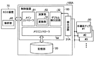
また、上述したように、近年では、モジュール内部にメモリや演算回路等を搭載するインテリジェントパワーモジュールが存在する。そこで、第8の実施形態では、上述した実施形態に係る検査装置をインテリジェントパワーモジュールとした場合について、図面を用いて詳細に説明する。なお、本実施形態では、図8に示した検査装置100をインテリジェントパワーモジュールとした場合を例示するが、これに限らず、例えば図12に示す検査装置200や図13に示す検査装置300に対しても適用することが可能である。また、本実施形態において、上述した実施形態と同様の構成については、それらを引用することで、重複する説明を省略する。
Claims (20)
- 応力負荷方向に対して電気抵抗の変化率が異なる複数の半導体チップに接続され、各半導体チップに流れた電流から各半導体チップの電気抵抗値を検出する検出部と、
電気抵抗値を温度、応力及びひずみのうちの少なくとも1つを示す特性値に変換するためのモデルデータを保持する第1記憶部と、
前記検出部で検出された各半導体チップの電気抵抗値を前記第1記憶部に保持された前記モデルデータを用いて前記特性値に変換する変換部と、
前記変換部で変換された前記特性値を前記複数の半導体チップごとの時系列データとして蓄積する第2記憶部と、
を備える、半導体チップの検査装置。 - 前記検出部で取得された各半導体チップの前記電気抵抗値を前記複数の半導体チップごとの時系列データとして保存する第3記憶部をさらに備える請求項1に記載の半導体チップの検査装置。
- 前記モデルデータは、前記電気抵抗値の変化率を前記特性値に変換する変換式である請求項1に記載の半導体チップの検査装置。
- 前記変換式は、電気抵抗の変化率に対して、温度と、各方向の応力成分と、各方向のひずみ成分とのうちの少なくとも1つを含む請求項3に記載の半導体チップの検査装置。
- 各方向の前記応力成分は、熱応力の成分と、実装応力の成分と、外力の成分とのうちの少なくとも1つを含む請求項4に記載の半導体チップの検査装置。
- 各方向の前記ひずみ成分は、熱ひずみの成分と、実装によるひずみの成分と、外力によるひずみの成分とのうちの少なくとも1つを含む請求項4に記載の半導体チップの検査装置。
- 前記変換式は、温度と応力−抵抗変化率との関係を示す係数を含む請求項5に記載の半導体チップの検査装置。
- 前記変換部は、前記外力及び前記実装応力が既知である場合、前記変換式を用いて前記電気抵抗の変化率から前記温度を特定する請求項5に記載の半導体チップの検査装置。
- 前記変換部は、前記温度が既知であって且つ前記外力が既知である場合、前記変換式を用いて前記実装応力を特定する請求項5に記載の半導体チップの検査装置。
- 前記変換部は、前記温度が既知であって且つ前記実装応力が既知である場合、前記変換式を用いて前記外力を特定する請求項5に記載の半導体チップの検査装置。
- 各半導体チップの電気抵抗の変化量をΔRonとし、各半導体チップに応力が印加されていない状態での電気抵抗値をRonとし、各半導体チップに応力を印加した際の電気抵抗の変化率をrpとした場合、前記変換式は、以下の式(1)で与えられる
- 温度と応力−抵抗変化率との関係を示す係数をαとし、応力と抵抗変化率との関係を示す係数をβとし、温度と熱応力との関係を示す係数をγとし、外力をσoとし、実装応力をσfとし、ジャンクション温度をTjとし、基準温度をT0とした場合、前記式(1)における前記電気抵抗の変化率rpは、以下の式(2)で表される
- 各半導体チップは、炭化シリコン基板を含み、前記炭化シリコン基板の<11−20>方向が主要な応力負荷方向と平行になるように配置されている請求項1に記載の半導体チップの検査装置。
- 前記第2記憶部に蓄積された前記複数の半導体チップごとの前記特性値の前記時系列データを用いて各半導体チップの故障確率を計算する解析部をさらに備える請求項1に記載の半導体チップの検査装置。
- 1つ以上のセンサと、
前記1つ以上のセンサで得られた情報と前記特性値とを比較し、当該比較の結果に基づいて、前記第1記憶部に保持されている前記モデルデータを修正する演算部と、
を更に備える請求項1に記載の半導体チップの検査装置。 - 前記演算部は、前記1つ以上のセンサで得られた前記情報と前記特性値とのうちの少なくとも1つを用いて解析処理を実行する機能を備え、
前記第1記憶部は、前記解析処理を実行する際に前記演算部が使用するパラメータを格納する
請求項15に記載の半導体チップの検査装置。 - 応力負荷方向に対して電気抵抗の変化率が異なる複数の半導体チップに接続され、各半導体チップに流れた電流から各半導体チップの電気抵抗値を検出する検出部と、
電気抵抗値を温度、応力及びひずみのうちの少なくとも1つを示す特性値に変換するためのモデルデータを保持する第1記憶部と、
前記検出部で検出された各半導体チップの電気抵抗値を前記第1記憶部に保持された前記モデルデータを用いて前記特性値に変換する変換部と、
前記変換部で変換された前記特性値を前記複数の半導体チップごとの時系列データとして蓄積する第2記憶部と、
を備える、半導体チップの検査システム。 - 応力負荷方向に対して電気抵抗の変化率が異なる複数の半導体素子形成領域と、
各半導体素子形成領域に流れた電流から各半導体素子形成領域の電気抵抗値を検出する検出部と、
電気抵抗値を温度、応力及びひずみのうちの少なくとも1つを示す特性値に変換するためのモデルデータを保持する第1記憶部と、
前記検出部で検出された各半導体素子形成領域の電気抵抗値を前記第1記憶部に保持された前記モデルデータを用いて前記特性値に変換する変換部と、
前記変換部で変換された前記特性値を前記複数の半導体素子形成領域ごとの時系列データとして蓄積する第2記憶部と、
を備えるインテリジェントパワーモジュール。 - 応力負荷方向に対して電気抵抗の変化率が異なる複数の半導体チップそれぞれに流れた電流から各半導体チップの電気抵抗値を検出し、
前記検出された各半導体チップの電気抵抗値を、電気抵抗値を温度、応力及びひずみのうちの少なくとも1つを示す特性値に変換するためのモデルデータを用いて特性値に変換し、
前記変換により得られた前記特性値を前記複数の半導体チップごとの時系列データとして蓄積し、
前記蓄積された前記複数の半導体チップごとの前記時系列データを解析する、
半導体チップの検査方法。 - 応力負荷方向に対して電気抵抗の変化率が異なる複数の半導体チップに接続された半導体チップの検査装置が備えるプロセッサを機能させるためのプログラムであって、
前記複数の半導体チップそれぞれに流れた電流から各半導体チップの電気抵抗値を検出し、
前記検出された各半導体チップの電気抵抗値を、電気抵抗値を温度、応力及びひずみのうちの少なくとも1つを示す特性値に変換するためのモデルデータを用いて特性値に変換し、
前記変換により得られた前記特性値を前記複数の半導体チップごとの時系列データとして蓄積する
ことを前記プロセッサに実行させるためのプログラム。
Priority Applications (2)
| Application Number | Priority Date | Filing Date | Title |
|---|---|---|---|
| JP2018006678A JP6957367B2 (ja) | 2018-01-18 | 2018-01-18 | 半導体チップの検査装置、半導体チップの検査システム、インテリジェントパワーモジュール、半導体チップの検査方法及びプログラム |
| US16/117,279 US11079427B2 (en) | 2018-01-18 | 2018-08-30 | Inspection device, inspection system, intelligent power module, inspection method, and computer program product |
Applications Claiming Priority (1)
| Application Number | Priority Date | Filing Date | Title |
|---|---|---|---|
| JP2018006678A JP6957367B2 (ja) | 2018-01-18 | 2018-01-18 | 半導体チップの検査装置、半導体チップの検査システム、インテリジェントパワーモジュール、半導体チップの検査方法及びプログラム |
Publications (2)
| Publication Number | Publication Date |
|---|---|
| JP2019124638A JP2019124638A (ja) | 2019-07-25 |
| JP6957367B2 true JP6957367B2 (ja) | 2021-11-02 |
Family
ID=67213803
Family Applications (1)
| Application Number | Title | Priority Date | Filing Date |
|---|---|---|---|
| JP2018006678A Active JP6957367B2 (ja) | 2018-01-18 | 2018-01-18 | 半導体チップの検査装置、半導体チップの検査システム、インテリジェントパワーモジュール、半導体チップの検査方法及びプログラム |
Country Status (2)
| Country | Link |
|---|---|
| US (1) | US11079427B2 (ja) |
| JP (1) | JP6957367B2 (ja) |
Families Citing this family (2)
| Publication number | Priority date | Publication date | Assignee | Title |
|---|---|---|---|---|
| JP7236231B2 (ja) * | 2018-09-07 | 2023-03-09 | ルネサスエレクトロニクス株式会社 | 半導体装置及び解析システム |
| GB2632292A (en) * | 2023-07-31 | 2025-02-05 | Aquatec Group Ltd | Strain monitoring of submerged structures |
Family Cites Families (13)
| Publication number | Priority date | Publication date | Assignee | Title |
|---|---|---|---|---|
| JPS5510993B1 (ja) * | 1969-08-07 | 1980-03-21 | ||
| JPS55113904A (en) * | 1979-02-26 | 1980-09-02 | Hitachi Ltd | Method of zero point temperature compensation for strain-electric signal transducer |
| JPH01290948A (ja) | 1988-05-19 | 1989-11-22 | Toyota Motor Corp | 内燃機関の制御装置 |
| JPH04307331A (ja) | 1991-04-02 | 1992-10-29 | Kayaba Ind Co Ltd | 複合センサ |
| JPH1164124A (ja) | 1997-08-25 | 1999-03-05 | Ishikawajima Harima Heavy Ind Co Ltd | 計測装置、荷重計測装置、計測方法及び荷重計測方法 |
| JP4011345B2 (ja) | 2002-01-11 | 2007-11-21 | 本田技研工業株式会社 | 多軸力センサチップ |
| US6823744B2 (en) | 2002-01-11 | 2004-11-30 | Honda Giken Kogyo Kabushiki Kaisha | Six-axis force sensor |
| JP4329477B2 (ja) | 2003-10-06 | 2009-09-09 | 株式会社日立製作所 | ひずみ量測定機能付きボルト |
| US20070246776A1 (en) * | 2006-04-20 | 2007-10-25 | Synopsys, Inc. | Stress engineering for cap layer induced stress |
| US7525162B2 (en) * | 2007-09-06 | 2009-04-28 | International Business Machines Corporation | Orientation-optimized PFETS in CMOS devices employing dual stress liners |
| US8352230B2 (en) * | 2010-03-12 | 2013-01-08 | International Business Machines Corporation | Integrated framework for finite-element methods for package, device and circuit co-design |
| TW201200853A (en) * | 2010-06-18 | 2012-01-01 | Ind Tech Res Inst | Measuring apparatus |
| US10101382B2 (en) * | 2016-12-30 | 2018-10-16 | Texas Instruments Incorporated | Systems and methods for dynamic Rdson measurement |
-
2018
- 2018-01-18 JP JP2018006678A patent/JP6957367B2/ja active Active
- 2018-08-30 US US16/117,279 patent/US11079427B2/en active Active
Also Published As
| Publication number | Publication date |
|---|---|
| JP2019124638A (ja) | 2019-07-25 |
| US20190219628A1 (en) | 2019-07-18 |
| US11079427B2 (en) | 2021-08-03 |
Similar Documents
| Publication | Publication Date | Title |
|---|---|---|
| Ugur et al. | A new complete condition monitoring method for SiC power MOSFETs | |
| Dusmez et al. | Aging precursor identification and lifetime estimation for thermally aged discrete package silicon power switches | |
| US11474145B2 (en) | Methods of determining operating conditions of silicon carbide power MOSFET devices associated with aging, related circuits and computer program products | |
| Oh et al. | Physics-of-failure, condition monitoring, and prognostics of insulated gate bipolar transistor modules: A review | |
| Pedersen et al. | Bond wire lift-off in IGBT modules due to thermomechanical induced stress | |
| Strauss et al. | Measuring the junction temperature of an IGBT using its threshold voltage as a temperature sensitive electrical parameter (TSEP) | |
| Arya et al. | Accurate online junction temperature estimation of IGBT using inflection point based updated I–V characteristics | |
| Degrenne et al. | A review of prognostics and health management for power semiconductor modules | |
| JP6957367B2 (ja) | 半導体チップの検査装置、半導体チップの検査システム、インテリジェントパワーモジュール、半導体チップの検査方法及びプログラム | |
| Reggiani et al. | Measurement and modeling of the electron impact-ionization coefficient in silicon up to very high temperatures | |
| Pfost et al. | Measurement and simulation of self-heating in DMOS transistors up to very high temperatures | |
| CN112818622A (zh) | 一种多芯片并联igbt模块可靠性综合评价方法及系统 | |
| Chou et al. | Thermal performance evaluation of cascode Paralleled-GaN-HEMTs packaging for high power switching applications | |
| US9383266B1 (en) | Test structure to monitor the in-situ channel temperature of field effect transistors | |
| Otto et al. | Reliability of new SiC BJT power modules for fully electric vehicles | |
| Li et al. | Study on Cauer Thermal Network Model Considering Bidirectional Heat Transfer | |
| Yang et al. | Study on the heat transfer of GaN-based high power HEMTs | |
| Chou et al. | Development and characterization of the thermal behavior of packaged cascode GaN HEMTs | |
| Hernando et al. | Thermal characterization of multichip power module | |
| Kosel et al. | Transient non-linear thermal FEM simulation of smart power switches and verification by measurements | |
| Catalano et al. | In-Situ Extraction of the Thermal Impedance of GaN Power HEMTs Embedded in PCB-based Power Circuits | |
| Kim | Thermal characterization of SiC MOSFETs for automotive power module | |
| Ma et al. | Systematic study on temperature and time-varying characteristics of SiC MOSFET static parameters at 200° C | |
| JP5157336B2 (ja) | パワー半導体素子の評価方法および評価装置 | |
| US20250200254A1 (en) | Characteristic prediction system |
Legal Events
| Date | Code | Title | Description |
|---|---|---|---|
| A621 | Written request for application examination |
Free format text: JAPANESE INTERMEDIATE CODE: A621 Effective date: 20200903 |
|
| A977 | Report on retrieval |
Free format text: JAPANESE INTERMEDIATE CODE: A971007 Effective date: 20210618 |
|
| A131 | Notification of reasons for refusal |
Free format text: JAPANESE INTERMEDIATE CODE: A131 Effective date: 20210629 |
|
| A521 | Request for written amendment filed |
Free format text: JAPANESE INTERMEDIATE CODE: A523 Effective date: 20210825 |
|
| TRDD | Decision of grant or rejection written | ||
| A01 | Written decision to grant a patent or to grant a registration (utility model) |
Free format text: JAPANESE INTERMEDIATE CODE: A01 Effective date: 20210907 |
|
| A61 | First payment of annual fees (during grant procedure) |
Free format text: JAPANESE INTERMEDIATE CODE: A61 Effective date: 20211006 |
|
| R151 | Written notification of patent or utility model registration |
Ref document number: 6957367 Country of ref document: JP Free format text: JAPANESE INTERMEDIATE CODE: R151 |