JP6956700B2 - Radiation detector - Google Patents
Radiation detector Download PDFInfo
- Publication number
- JP6956700B2 JP6956700B2 JP2018208802A JP2018208802A JP6956700B2 JP 6956700 B2 JP6956700 B2 JP 6956700B2 JP 2018208802 A JP2018208802 A JP 2018208802A JP 2018208802 A JP2018208802 A JP 2018208802A JP 6956700 B2 JP6956700 B2 JP 6956700B2
- Authority
- JP
- Japan
- Prior art keywords
- layer
- scintillator
- resin
- substrate
- radiation detector
- Prior art date
- Legal status (The legal status is an assumption and is not a legal conclusion. Google has not performed a legal analysis and makes no representation as to the accuracy of the status listed.)
- Active
Links
Images


Description
本発明は、放射線検出器に関する。 The present invention relates to a radiation detector.
当該分野の技術として特許文献1〜3が知られている。
特許文献1は、シンチレータパネルを開示する。シンチレータパネルは、樹脂基板と蛍光体層との間に設けられた金属膜を有する。
特許文献2は、シンチレータパネルを備える放射線検出装置を開示する。シンチレータパネルは、ヨウ化セシウムを主成分とするシンチレータ層を有する。このシンチレータ層には、タリウムがドープされている。シンチレータ層におけるタリウムの濃度は、基板との界面付近において大きくなっている。このタリウムの濃度分布によれば、光出力が向上する。
特許文献3は、蛍光体層を備える放射線検出器を開示する。この放射線検出器も、ヨウ化セシウムを主成分とするシンチレータ層を有し、当該シンチレータ層には、タリウムがドープされている。また、シンチレータ層におけるタリウムの濃度は、基板側が大きくなっている。このタリウムの濃度分布によれば、センサ基板と蛍光体層との密着性が向上する。
シンチレータ層を成長させる成長基板は、水分を透過する透湿性を有することがある。成長基板を透過した水分は、シンチレータ層の根元部に到達する。ヨウ化セシウムにより形成されたシンチレータ層は、潮解性を有することが知られている。そうすると、成長基板から供給された水分によって、シンチレータ層の根元部に潮解が生じ、ひいてはシンチレータパネルの特性が低下してしまう。従って、当該分野においては、ヨウ化セシウムにより形成されたシンチレータ層を有するシンチレータパネルの耐湿性の向上が望まれている。 The growth substrate on which the scintillator layer is grown may have moisture permeability to allow moisture to permeate. Moisture that has passed through the growth substrate reaches the root of the scintillator layer. The scintillator layer formed by cesium iodide is known to have deliquescent properties. Then, the moisture supplied from the growth substrate causes deliquescent at the root of the scintillator layer, which in turn deteriorates the characteristics of the scintillator panel. Therefore, in this field, it is desired to improve the moisture resistance of a scintillator panel having a scintillator layer formed of cesium iodide.
例えば、特許文献1では、基板と蛍光体層との間に金属膜を設けることにより、樹脂基板から蛍光体層への水分の移動を阻害することを狙っている。
For example,
そこで、本発明は、耐湿性を向上し得る放射線検出器を提供することを目的とする。 Therefore, an object of the present invention is to provide a radiation detector capable of improving moisture resistance.
本発明の一形態である放射線検出器は、有機材料を主成分として含むセンサ基板と、センサ基板上に形成され、有機材料からなる樹脂保護層と、樹脂保護層上に形成され、タリウムが添加されたヨウ化セシウムを主成分として含む複数の柱状結晶により構成されるシンチレータ層と、を備え、センサ基板は、シンチレータ層において生じた光を受ける光電変換素子が設けられた光検出面を有する。また、本発明の一形態であるシンチレータパネルは、基板と、基板上に形成され、有機材料からなる中間層と、中間層上に形成され、ヨウ化タリウムを主成分として含むバリア層と、バリア層上に形成され、タリウムが添加されたヨウ化セシウムを主成分として含む複数の柱状結晶により構成されるシンチレータ層と、を備える。 The photodetector, which is one embodiment of the present invention, is formed on a sensor substrate containing an organic material as a main component, a sensor substrate, a resin protective layer made of an organic material, and a resin protective layer, to which thallium is added. The sensor substrate includes a scintillator layer composed of a plurality of columnar crystals containing cesium iodide as a main component, and the sensor substrate has a photodetection surface provided with a photoelectric conversion element that receives light generated in the scintillator layer. Further, the scintillator panel, which is one embodiment of the present invention, has a substrate, an intermediate layer formed on the substrate and made of an organic material, a barrier layer formed on the intermediate layer and containing thallium iodide as a main component, and a barrier. It includes a scintillator layer formed on the layer and composed of a plurality of columnar crystals containing cesium iodide to which thallium is added as a main component.
このシンチレータパネルでは、シンチレータ層は、中間層とバリア層とを介して基板上に形成される。バリア層は、ヨウ化タリウムを主成分として含む。このようなバリア層は、水分を透し難い性質を有する。そうすると、有機材料からなる中間層からシンチレータ層へ移動しようとする水分を、バリア層によって阻止することが可能になる。これにより、シンチレータ層の根元部における潮解が抑制されるので、ひいてはシンチレータパネルの特性の低下を抑制できる。従って、シンチレータパネルの耐湿性を向上することができる。 In this scintillator panel, the scintillator layer is formed on the substrate via an intermediate layer and a barrier layer. The barrier layer contains thallium iodide as a main component. Such a barrier layer has a property that it is difficult for moisture to permeate. Then, the barrier layer can block the moisture that tends to move from the intermediate layer made of the organic material to the scintillator layer. As a result, deliquescent at the root of the scintillator layer is suppressed, and as a result, deterioration of the characteristics of the scintillator panel can be suppressed. Therefore, the moisture resistance of the scintillator panel can be improved.
上記のシンチレータパネルにおいて、基板は、金属材料、炭素材料、ガラス材料及び樹脂材料の何れか一つを主成分として含んでもよい。この構成によれば、基板に対して材料特性に基づく特性を付与することができる。 In the above scintillator panel, the substrate may contain any one of a metal material, a carbon material, a glass material and a resin material as a main component. According to this configuration, it is possible to impart properties based on material properties to the substrate.
上記のシンチレータパネルにおいて、有機材料は、キシリレン系樹脂、アクリル系樹脂、シリコーン系樹脂、ポリイミド又はポリエステル系樹脂の何れか一つを含んでもよい。この構成によれば、中間層に対して材料特性に基づく特性を付与することができる。 In the above scintillator panel, the organic material may contain any one of xylylene-based resin, acrylic-based resin, silicone-based resin, polyimide or polyester-based resin. According to this configuration, it is possible to impart properties based on material properties to the intermediate layer.
本発明の別の形態である放射線検出器は、基板と、基板上に形成され、有機材料からなる中間層と、中間層上に形成され、ヨウ化タリウムを主成分として含むバリア層と、バリア層上に形成され、タリウムが添加されたヨウ化セシウムを主成分として含む複数の柱状結晶により構成されるシンチレータ層と、を有するシンチレータパネルと、シンチレータパネルにおいて生じた光を受ける光電変換素子が設けられた光検出面を含むセンサ基板と、を備え、センサ基板の光検出面は、シンチレータ層と対面する。 The photodetector, which is another embodiment of the present invention, has a substrate, an intermediate layer formed on the substrate and made of an organic material, a barrier layer formed on the intermediate layer and containing thallium iodide as a main component, and a barrier. A scintillator panel having a scintillator layer formed on the layer and composed of a plurality of columnar crystals containing thallium-added cesium iodide as a main component, and a photoelectric conversion element that receives light generated in the scintillator panel are provided. A sensor substrate including the light detection surface is provided, and the light detection surface of the sensor substrate faces the scintillator layer.
この放射線検出器は、シンチレータパネルに入射した放射線によって光が生成され、当該光は光検出面に設けられた光電変換素子によって検出される。ここで、放射線検出器は、基板とシンチレータ層との間に、有機材料からなる中間層と、ヨウ化タリウムを主成分として含むバリア層を有する。このバリア層によれば、中間層からシンチレータ層への水分の移動を阻止することが可能になる。従って、シンチレータ層の根元部における潮解が抑制されるので、シンチレータパネルの特性の低下を抑制することが可能になる。その結果、放射線検出器は、放射線の検出特性の低下が抑制されるので、耐湿性を向上することができる。 In this radiation detector, light is generated by the radiation incident on the scintillator panel, and the light is detected by a photoelectric conversion element provided on the photodetection surface. Here, the radiation detector has an intermediate layer made of an organic material and a barrier layer containing thallium iodide as a main component between the substrate and the scintillator layer. According to this barrier layer, it becomes possible to prevent the movement of water from the intermediate layer to the scintillator layer. Therefore, since the deliquescent at the root of the scintillator layer is suppressed, it is possible to suppress the deterioration of the characteristics of the scintillator panel. As a result, the radiation detector can improve the moisture resistance because the deterioration of the radiation detection characteristic is suppressed.
上記の放射線検出器において、基板は、金属材料、炭素材料、ガラス材料及び樹脂材料の何れか一つを主成分として含んでもよい。この構成によれば、基板に対して材料特性に基づく特性を付与することができる。 In the above radiation detector, the substrate may contain any one of a metal material, a carbon material, a glass material and a resin material as a main component. According to this configuration, it is possible to impart properties based on material properties to the substrate.
上記の放射線検出器において、有機材料は、キシリレン系樹脂、アクリル系樹脂、シリコーン系樹脂、ポリイミド及びポリエステル系樹脂の何れか一つを含んでもよい。この構成によれば、中間層に対して材料特性に基づく特性を付与することができる。 In the above radiation detector, the organic material may contain any one of xylylene-based resin, acrylic-based resin, silicone-based resin, polyimide and polyester-based resin. According to this configuration, it is possible to impart properties based on material properties to the intermediate layer.
本発明のさらに別の形態である放射線検出器は、基板と、基板上に形成され、有機材料からなる中間層と、中間層上に形成され、ヨウ化タリウムを主成分として含むバリア層と、バリア層上に形成され、タリウムが添加されたヨウ化セシウムを主成分として含む複数の柱状結晶により構成されるシンチレータ層と、を備え、基板は、シンチレータ層において生じた光を受ける光電変換素子が設けられた光検出面を有する。 The photodetector, which is still another form of the present invention, includes a substrate, an intermediate layer formed on the substrate and made of an organic material, and a barrier layer formed on the intermediate layer containing thallium iodide as a main component. A scintillator layer formed on the barrier layer and composed of a plurality of columnar crystals containing thallium-added cesium iodide as a main component is provided, and the substrate is a photoelectric conversion element that receives light generated in the scintillator layer. It has a provided light detection surface.
この放射線検出器は、シンチレータパネルに入射した放射線によって光が生成され、当該光は光検出面に設けられた光電変換素子によって検出される。ここで、放射線検出器は、基板とシンチレータ層との間に、有機材料からなる中間層と、ヨウ化タリウムを主成分として含むバリア層を有する。このバリア層によれば、中間層からシンチレータ層への水分の移動を阻止することが可能になる。従って、シンチレータ層の根元部における潮解が抑制されるので、シンチレータパネルの特性の低下を抑制することが可能になる。その結果、放射線検出器は、放射線の検出特性の低下が抑制されるので、耐湿性を向上することができる。 In this radiation detector, light is generated by the radiation incident on the scintillator panel, and the light is detected by a photoelectric conversion element provided on the photodetection surface. Here, the radiation detector has an intermediate layer made of an organic material and a barrier layer containing thallium iodide as a main component between the substrate and the scintillator layer. According to this barrier layer, it becomes possible to prevent the movement of water from the intermediate layer to the scintillator layer. Therefore, since the deliquescent at the root of the scintillator layer is suppressed, it is possible to suppress the deterioration of the characteristics of the scintillator panel. As a result, the radiation detector can improve the moisture resistance because the deterioration of the radiation detection characteristic is suppressed.
上記の放射線検出器において、基板は、金属材料、炭素材料及びガラス材料の何れか一つを主成分として含んでもよい。この構成によれば、基板に対して材料特性に基づく特性を付与することができる。 In the above radiation detector, the substrate may contain any one of a metal material, a carbon material and a glass material as a main component. According to this configuration, it is possible to impart properties based on material properties to the substrate.
上記の放射線検出器において、有機材料は、キシリレン系樹脂、アクリル系樹脂、シリコーン系樹脂、ポリイミド、ポリエステル系樹脂、シロキサン樹脂及びエポキシ樹脂の何れか一つを含んでもよい。この構成によれば、中間層に対して材料特性に基づく特性を付与することができる。 In the above radiation detector, the organic material may contain any one of xylylene-based resin, acrylic-based resin, silicone-based resin, polyimide, polyester-based resin, siloxane resin, and epoxy resin. According to this configuration, it is possible to impart properties based on material properties to the intermediate layer.
本発明によれば、耐湿性を向上し得るシンチレータパネル及び放射線検出器が提供される。 According to the present invention, a scintillator panel and a radiation detector capable of improving moisture resistance are provided.
以下、添付図面を参照しながら本発明を実施するための形態を詳細に説明する。図面の説明において同一の要素には同一の符号を付し、重複する説明を省略する。 Hereinafter, embodiments for carrying out the present invention will be described in detail with reference to the accompanying drawings. In the description of the drawings, the same elements are designated by the same reference numerals, and duplicate description will be omitted.
<第1実施形態>
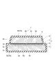
図1に示されるように、第1実施形態に係るシンチレータパネル1は、基板2と、樹脂保護層5(中間層)と、バリア層3と、シンチレータ層4と、保護膜6と、を有する。このような構成を有するシンチレータパネル1は、光電変換素子(不図示)と組み合わされて放射線イメージセンサとして用いられる。
<First Embodiment>
As shown in FIG. 1, the
基板2、樹脂保護層5、バリア層3及びシンチレータ層4は、それぞれの厚み方向に沿ってこの順に積層された積層体7である。具体的には、基板2上に樹脂保護層5が形成される。次に、樹脂保護層5上にバリア層3が形成される。そして、バリア層3上にシンチレータ層4が形成される。つまり、基板2とシンチレータ層4との間には、樹脂保護層5とバリア層3とが存在するので、基板2とシンチレータ層4とが直接に接することはない。積層体7は、保護膜6により覆われる。
The
基板2は、シンチレータパネル1の基体をなす。基板2は、平面視して矩形、多角形又は円形を呈し、その厚さは、10マイクロメートル以上5000マイクロメートル以下であり、一例として100マイクロメートルである。基板2は、基板表面2aと、基板裏面2bと、基板側面2cとを有する。基板2は、金属材料、炭素材料、セラミックス材料又は樹脂材料からなる。金属材料として、例えば、アルミニウム、ステンレス鋼(SUS)、銅が挙げられる。また、炭素材料として、例えば、アモルファスカーボンが挙げられ、セラミックス材料として、例えば、ガラスやアルミナが挙げられ、樹脂材料として、例えば、ポリエチレンテレフタレート、ポリエチレンナフタレート、ポリイミド、ポリエーテルエーテルケトンが挙げられる。
The
樹脂保護層5は、基板2が金属材料からなる場合、基板2に対するシンチレータ層4の直接接触を妨げることにより、基板2がシンチレータ層4に直接接触することに起因する金属基板2の腐食を防止する。従って、樹脂保護層5は、少なくともシンチレータ層4よりも大きい面積を有する。又、基板2が炭素材料、セラミックス材料、樹脂材料からなる場合、基板2上に樹脂保護層5を設けることで複数の柱状結晶により構成されるシンチレータ層4の根元部分の基板2に対する膜付きがよくなり、きれいな柱状結晶を成長させることができる。樹脂保護層5は、保護層表面5aと、保護層裏面5bと、保護層側面5cと、を有する。保護層表面5aは、バリア層3と対面する。保護層裏面5bは、基板表面2aと対面する。保護層側面5cは、基板側面2cと面一である。本実施形態においては、樹脂保護層5は、基板表面2aの全面に形成される。また、樹脂保護層5は、基板表面2aだけでなく、基板裏面2b及び基板側面2c上を覆ってもよい。つまり、樹脂保護層5は、基板2の全体を覆ってもよい。樹脂保護層5は、樹脂材料からなる。樹脂材料として、ポリパラキシリレン等のキシリレン系樹脂、アクリル系樹脂、シリコーン系樹脂、ポリイミド、ポリエステル系樹脂が挙げられる。
When the
バリア層3は、樹脂保護層5からシンチレータ層4への水分の移動を阻害する。バリア層3は、保護層表面5aの一部の領域上に形成される。つまり、厚み方向からみたとき、バリア層3は、樹脂保護層5及び基板2よりも小さい。バリア層3の厚みは0.001マイクロメートル以上1.0マイクロメートル以下であり、一例として0.06マイクロメートル(600オングストローム)である。バリア層3は、バリア層表面3aと、バリア層裏面3bと、バリア層側面3cと、を有する。バリア層表面3aは、シンチレータ層4と対面する。バリア層裏面3bは、保護層表面5aと対面する。バリア層3は、ヨウ化タリウム(TlI)を主成分として含む。例えば、バリア層3のTlI含有量は、90%以上100%以下であってもよい。換言すると、バリア層3におけるTlI含有量が90%以上である場合に、バリア層3はTlIを主成分とするものといってよい。このようなバリア層3は、例えば、二源蒸着法によって形成することができる。具体的には、ヨウ化セシウム(CsI)を収容する第1蒸着源と、ヨウ化タリウム(TlI)を収容する第2蒸着源と、を利用する。CsIよりも先にTlIを基板に蒸着することでバリア層3を形成する。その厚みは、一例として600オングストローム程度である。尚、バリア層の膜厚は、強粘着テープ等でシンチレータ層と基板とを剥離し、基板界面を蛍光X線分析(XRF)装置にて分析することで測定できる。装置としては例えばリガク社のZSX Primusを挙げることができる。
The
シンチレータ層4は、放射線を受けて、当該放射線に対応する光を発生させる。シンチレータ層4は、その厚さが10マイクロメートル以上3000マイクロメートル以下であり、一例として600マイクロメートルである。シンチレータ層4は、蛍光体材料であって、タリウムが添加されたヨウ化セシウムを主成分として含む。つまり、ヨウ化セシウムは、タリウムをドーパントとして含む(CsI:Tl)。例えば、シンチレータ層4のCsI含有量は、90%以上100%以下であってもよい。換言すると、シンチレータ層4のCsI含有量が90%以上である場合に、シンチレータ層4はCsIを主成分とするものといってよい。更に、シンチレータ層4は複数の柱状結晶により構成されるため、各柱状結晶がライトガイド効果を有することで高解像度のイメージングに適している。このようなシンチレータ層4は、例えば、蒸着法によって形成することができる。
The
シンチレータ層4は、シンチレータ層表面4aと、シンチレータ層裏面4bと、シンチレータ層側面4cとを有する。シンチレータ層4は、シンチレータ層裏面4bがバリア層表面3aと対面するように、バリア層3上に形成される。つまり、シンチレータ層4と樹脂保護層5との間には、バリア層3が存在する。従って、シンチレータ層4は、樹脂保護層5に直接に接触することはない。また、厚み方向から見てバリア層3は、基板2及び樹脂保護層5よりも小さい。従って、シンチレータ層4も同様に、厚み方向から見てシンチレータ層4は、基板2及び樹脂保護層5よりも小さい。
The
シンチレータ層4は、その厚み方向に延びる複数の柱状結晶を含む。複数の柱状結晶の根元部は、シンチレータ層裏面4bを構成し、バリア層3のバリア層表面3aと接する。また、複数の柱状結晶の先端部は、シンチレータ層表面4aを構成する。
The
さらに、シンチレータ層4は角錐台形状を呈しており、シンチレータ層側面4cはその厚み方向に対して傾く。換言すると、シンチレータ層側面4cは、スロープ(傾斜)を有する。具体的には、シンチレータ層4を厚み方向に直交する方向から断面視したとき、断面は台形状を呈する。つまり、シンチレータ層表面4a側の一辺は、シンチレータ層裏面4b側の一辺よりも短い。
Further, the
保護膜6は、積層体7を覆うことにより積層体7を湿気から保護する。保護膜6は、基板裏面2b、基板側面2c、保護層側面5c、バリア層側面3c、シンチレータ層側面4c及びシンチレータ層表面4aを覆う。また、保護膜6の厚みは、形成される全ての箇所において略同じであってもよいし、箇所ごとに異なっていてもよい。例えば、保護膜6によれば、例えば、シンチレータ層表面4aの上に形成された膜部は、基板裏面2b、基板側面2c、バリア層側面3c、シンチレータ層側面4cの上に形成された膜部よりも厚い。保護膜6は、ポリパラキシリレンを主成分とする。このような保護膜6は、例えば化学気相成長法(CVD)により形成できる。
The
このシンチレータパネル1では、樹脂保護層5とシンチレータ層4との間にバリア層3が設けられる。バリア層3は、ヨウ化タリウムを主成分として含む。このようなバリア層3は、水分を透し難い性質を有する。そうすると、樹脂保護層5からシンチレータ層4へ移動しようとする水分を、バリア層3によって阻止することが可能になる。これにより、シンチレータ層4の根元部における潮解が抑制されるので、ひいてはシンチレータパネル1の特性の低下を抑制できる。従って、シンチレータパネル1の耐湿性を向上することができる。
In the
<第2実施形態>
次に、第2実施形態に係る放射線検出器について説明する。尚、実際にはセンサパネル11上には導通を取るための領域(辺)が設けられるが、便宜上図示していない。
<Second Embodiment>
Next, the radiation detector according to the second embodiment will be described. Actually, a region (side) for taking conduction is provided on the
図2に示されるように、放射線検出器10は、センサパネル11(センサ基板)と、樹脂保護層5と、バリア層3と、シンチレータ層4と、封止部12と、を有する。封止板14から受け入れられた放射線が、シンチレータ層4に入射する。シンチレータ層4は、放射線に応じた光を発生させる。当該光は、樹脂保護層5及びバリア層3を通過してセンサパネル11に入射する。センサパネル11は、入射した光に応じて電気信号を発生させる。当該電気信号は、所定の電気回路を通じて出力される。この電気信号によれば、放射線イメージ画像が得られる。
As shown in FIG. 2, the
センサパネル11は、パネル表面11aと、パネル裏面11bと、パネル側面11cと、を有する。センサパネル11は、光電変換素子16を有するCCDセンサ、CMOSセンサ又はTFTパネルであり、シリコン等の半導体又はガラスを主成分として含む。なお、センサパネル11は、有機材料を主成分として含んでもよい。有機材料として、例えば、ポリエチレンテレフタレート(PET)、ポリエチレンナフタレート(PEN)、ポリイミド(PI)が挙げられる。複数の光電変換素子16は、パネル表面11a上において二次元状に配置される。複数の光電変換素子16が配置されたパネル表面11a上の領域は、光検出領域S1(光検出面)である。そして、パネル表面11aは、光検出領域S1に加えて、当該光検出領域S1を囲む周囲領域S2を含む。上記の光電変換素子16を保護するために、樹脂保護層5が設けられる。樹脂保護層5は、例えば、ポリイミド、シロキサン樹脂又はエポキシ樹脂である。又、複数の柱状結晶よりなるシンチレータ層の結晶性を高めるために、第1実施形態と同様の樹脂保護層5を設けてもよい。
The
封止部12は、センサパネル11の保護層裏面5bの一部と、バリア層3と、シンチレータ層4と、を覆う。封止部12は、保護層裏面5bにおける周囲領域S2に固定される。そして、封止部12と樹脂保護層5によって形成される内部空間を気密に保つ。この構成により、シンチレータ層4が湿気から保護される。
The sealing
封止部12は、封止枠13と、封止板14と、を有する。封止枠13は、枠表面13aと、枠裏面13bと、枠壁部13cと、を有する。枠壁部13cは、枠表面13aと枠裏面13bとを連結する。枠壁部13cの高さ(つまり枠表面13aから枠裏面13bまでの長さ)は、保護層裏面5bからシンチレータ層裏面4bまでの高さよりも高い。従って、シンチレータ層裏面4bと封止板14との間には隙間が形成される。封止枠13は、例えば、樹脂材料、金属材料、セラミック材料により構成してよい。封止枠13は中実であっても、中空であってもよい。枠表面13aと板裏面14b、枠裏面13bと樹脂保護層5とを接着剤によって接合してもよい。
The sealing
封止板14は、平面視して矩形状の板材である。封止板14は、板表面14aと、板裏面14bと、板側面14cとを有する。板裏面14bは、枠表面13aに対して固定される。板側面14cは、枠壁部13cの外側面に対して面一であってもよい。封止板14は、例えば、ガラス材料、金属材料、カーボン材料、バリアフィルムにより構成してよい。金属材料としては、アルミニウムが例示される。カーボン材料としては、CFRPが例示される。バリアフィルムとしては、有機材料層(PETやPEN)と無機材料層(SiN)との積層体が例示される。
The sealing
放射線検出器10は、シンチレータ層4に入射した放射線によって光が生成され、当該光は光検出領域S1に設けられた光電変換素子16によって検出される。ここで、放射線検出器10は、樹脂保護層5とシンチレータ層4との間に、ヨウ化タリウムを主成分として含むバリア層3を有する。このバリア層3によれば、樹脂保護層5からシンチレータ層4への水分の移動を阻止することが可能になる。従って、シンチレータ層4の根元部における潮解が抑制されるので、放射線検出器10の特性の低下を抑制することができる。
In the
以上、本発明の実施形態について説明したが、上記実施形態に限定されることなく様々な形態で実施される。変形例1〜3は、第1実施形態の変形例である。また、変形例4〜9は、第2実施形態の変形例である。
Although the embodiment of the present invention has been described above, the embodiment is not limited to the above embodiment and may be implemented in various forms.
<変形例1>
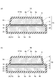
図3の(a)部は、変形例1に係るシンチレータパネル1Aを示す。変形例1に係るシンチレータパネル1Aは、基板2Aと、樹脂反射層5Aと、バリア層3と、シンチレータ層4と、保護膜6と、を有する。基板2Aは、その構成材料に特に限定がない。基板2Aは、金属材料、炭素材料に加えて、さらにガラス材料や樹脂材料により構成してよい。金属材料として、例えば、アルミニウム、ステンレス鋼(SUS)が挙げられる。炭素材料として、例えば、アモルファスカーボン、炭素繊維強化プラスチック(CFRP)が挙げられる。樹脂材料として、例えば、ポリエチレンテレフタレート(PET)、ポリエチレンナフタレート(PEN)、ポリイミド(PI)が挙げられる。樹脂反射層5Aは、シンチレータ層4において生じた光を反射する。樹脂反射層5Aは、例えば、白色顔料とバインダー樹脂の混合材料により構成してよい。白色顔料としては、例えば、アルミナ、酸化チタン、酸化イットリウム、酸化ジルコニウムが挙げられる。保護膜6は、ポリパラキシリレンによって構成してよい。保護膜6は、化学気相成長法(CVD法)によって形成される。
<Modification example 1>
Part (a) of FIG. 3 shows the
<変形例2>
図3の(b)部は、変形例2に係るシンチレータパネル1Bを示す。変形例2に係るシンチレータパネル1Bは、基板2と、無機反射層8と、樹脂保護層5と、バリア層3と、シンチレータ層4と、保護膜6と、を有する。つまり、変形例2に係るシンチレータパネル1Bは、第1実施形態に係るシンチレータパネル1に、無機反射層8を追加したものである。無機反射層8は、基板2と樹脂保護層5との間に形成される。具体的には、無機反射層8は、反射層表面8aと、反射層裏面8bと、反射層側面8cと、を有する。そして、反射層表面8aは、保護層裏面5bと対面する。反射層裏面8bは、基板表面2aと対面する。無機反射層8は、例えば、金属材料により構成されてもよい。金属材料として、例えば、アルミニウム、銀が挙げられる。また、無機反射層8は、誘電体多層膜であってもよい。誘電体多層膜は、酸化シリコン(SiO2)と酸化チタン(TiO2)との積層膜である。樹脂保護層5は、例えば、ポリイミド(PI)、ポリパラキシリレンが挙げられる。このシンチレータパネル1Bによれば、無機反射層8において、シンチレータ層4において生じた光を反射することができる。さらに、シンチレータ層4と無機反射層8との間には、樹脂保護層5が形成される。この樹脂保護層5によれば、金属材料により構成された無機反射層8のシンチレータ層4への直接接触を阻害する。従って、無機反射層8のシンチレータ層4への直接接触に起因する無機反射層8の腐食の発生を抑制できる。又、無機反射層8が誘電体多層膜からなる場合、樹脂保護層5を設けることで誘電体多層膜にピンホールがある場合の金属基板の腐食の発生を抑制できる。
<
Part (b) of FIG. 3 shows the
<変形例3>
図4の(a)部は、変形例3に係るシンチレータパネル1Cを示す。シンチレータパネル1Cは、基板2Bと、樹脂反射層5Aと、バリア層3と、シンチレータ層4と、樹脂膜9と、を有する。基板2Bは、薄いガラス材料(例えば150μm以下の厚さ)又はCFRPといった炭素材料により構成される。このような基板2Bは、反りやすい性質を有する。そこで、シンチレータ層形成時に基板2Bの反りを抑制するために、樹脂膜9を形成する。具体的には、基板2Bの基板裏面2bの全面に樹脂膜9を形成する。樹脂膜9は、樹脂材料により構成されたシート部材であり、当該シート部材を基板裏面2bに貼りあわせてもよい。また、樹脂膜9は、樹脂材料を塗布した後に、乾燥させて形成したものであってもよい。この構成によれば、基板2Bの反りの発生を抑制できる。
<Modification example 3>
Part (a) of FIG. 4 shows the
<変形例4>
図4の(b)部は、変形例4に係る放射線検出器10Aを示す。放射線検出器10Aは、第2実施形態に係る放射線検出器10とは異なる封止部12Aを有する。その他のバリア層3、シンチレータ層4、樹脂保護層5及びセンサパネル11の構成は、第2実施形態に係る放射線検出器10と同様である。封止部12Aは、封止板14と封止枠13Aとを備えており、封止枠13Aはさらに、内側封止枠17と外側封止枠18とを有する。つまり、封止枠13は二重構造を有する。内側封止枠17は、例えば、樹脂材料により構成してよい。また、外側封止枠18は、例えば、無機材料により形成されたコーティング層や、ガラスロッドといった無機固形材料により構成してもよい。この構成によれば、シンチレータ層4を湿気から好適に保護することができる。
<Modification example 4>
Part (b) of FIG. 4 shows the
<変形例5>
図5の(a)部は、変形例5に係る放射線検出器10Bを示す。放射線検出器10Bは、第2実施形態に係る放射線検出器10に対して、封止部12を有しておらず、封止部12に代えて保護膜6Aを有する。その他のバリア層3、シンチレータ層4及びセンサパネル11の構成は、第2実施形態に係る放射線検出器10と同様である。保護膜6Aは、保護層裏面5bと、バリア層側面3cと、シンチレータ層側面4cと、シンチレータ層裏面4bとを覆う。この構成によれば、保護膜6Aは、シンチレータ層4Aを湿気から保護することができる。尚、保護膜6Aは保護膜6と同様の材料から選択することができる。
<
Part (a) of FIG. 5 shows the
<変形例6>
図5の(b)部は、変形例6に係る放射線検出器10Cを示す。放射線検出器10Cは、変形例5に係る放射線検出器10Bに対して、さらに封止枠13Bを追加したものである。従って、シンチレータ層4、バリア層3、樹脂保護層5、センサパネル11及び保護膜6Aは、変形例5に係る放射線検出器10Bと同様である。封止枠13Bは、樹脂保護層5と保護膜6Aの接合部を塞ぐように形成される。従って、封止枠13Bは、厚み方向から平面視すると、保護膜6Aの外縁に沿って形成される。封止枠13Bは、例えば、UV硬化樹脂により構成してよい。この構成によれば、センサパネル11と保護膜6Aの接合部からの湿気の侵入が抑制されるので、耐湿性をさらに高めることができる。
<
Part (b) of FIG. 5 shows the
<変形例7>
図6の(a)部は、変形例7に係る放射線検出器10Dを示す。放射線検出器10Dは、第2実施形態に係る放射線検出器10の封止部12を有しておらず、封止部12に代えて封止シート12Bを有する。その他のバリア層3、シンチレータ層4、樹脂保護層5及びセンサパネル11の構成は、第2実施形態に係る放射線検出器10と同様である。封止シート12Bは、厚み方向に平面視して矩形、多角形又は円形を呈する。封止シート12Bは、例えば、金属箔、アルミニウムシートといった金属シート、バリアフィルムにより構成してよい。封止シート12Bは、シンチレータ層4及びバリア層3を覆う。具体的には、シンチレータ層裏面4b、シンチレータ層側面4c、バリア層側面3c及び保護層裏面5bの一部を覆う。すなわち、平面視した場合に、封止シート12Bは、シンチレータ層4及びバリア層3よりも大きい。そして、封止シート12Bの外周縁12aは、保護層裏面5bに対して接着剤15により接着される。従って、封止シート12B及び樹脂保護層5は、シンチレータ層4及びバリア層3を収容する気密領域を形成する。従って、シンチレータ層4を湿気から保護することができる。なお、接着剤15は、フィラー材を含んでもよい。このフィラー材は、接着層よりも厚さ未満の粒径を有する。
<
Part (a) of FIG. 6 shows the
<変形例8>
図6の(b)部は、変形例8に係る放射線検出器10Eを示す。放射線検出器10Eは、変形例7に係る封止シート12Bとは異なる構成の封止枠12Cを有する。封止枠12Cは、箱状を呈し、底面に開口を有する。すなわち、変形例7に係る封止シート12Bは柔軟性を有するが、変形例8に係る封止枠12Cは所定の形状を保ち、硬質である点で相違する。従って、封止枠12Cは、例えば、ガラス材料、金属材料、カーボン材料により構成してよい。封止枠12Cは、その底面が保護層裏面5bに対して接着剤15により接着される。この構成によれば、シンチレータ層4が封止枠12Cと樹脂保護層5とが形成する気密領域に配置されるので、シンチレータ層4を湿気から保護することができる。さらに、封止枠12Cが硬質であるので、シンチレータ層4を機械的に保護することができる。
<
Part (b) of FIG. 6 shows the
<変形例9>
図7の(a)部は、変形例9に係る放射線検出器10Fを示す。放射線検出器10Fは、第2実施形態に係る放射線検出器10とは異なるバリア層3A、シンチレータ層4A及び樹脂保護層5Bを有する。バリア層3Aは、バリア層表面3aと、バリア層裏面3bと、バリア層側面3cと、を有する。シンチレータ層4Aは、シンチレータ層表面4aと、シンチレータ層裏面4bと、シンチレータ層側面4cと、を有する。樹脂保護層5Bは、保護層表面5aと、保護層裏面5bと、保護層側面5cと、を有する。センサパネル11の単体構成は、第2実施形態に係る放射線検出器10と同様である。シンチレータ層4Aは、センサパネル11の一側面において、光検出領域S1からはみ出すように形成される。具体的には、まず、樹脂保護層5Bは、光検出領域S1と、一方の周辺領域S2a上に形成される。次に、バリア層3Aは、樹脂保護層5Bを覆うように、光検出領域S1と、一方のパネル側面11cと、光検出領域S1と一方のパネル側面11cとの間の周辺領域S2aと、の上に形成される。そして、シンチレータ層4Aは、バリア層3Aを覆うように、バリア層3Aの全面上に形成される。この構成を有する放射線検出器10Fは、例えば、シンチレータ層4Aが光検出領域S1をはみ出すように形成された辺を胸壁側に配置することでマンモグラフィー用の放射線検出器として好適に用いることができる。
<Modification example 9>
Part (a) of FIG. 7 shows the
<変形例10>
図7の(b)部は、変形例10に係る放射線検出器10Gを示す。変形例10に係る放射線検出器10Gは、基板2と、樹脂保護層5と、バリア層3と、シンチレータ層4と、センサパネル11と、を有する。
<Modification example 10>
Part (b) of FIG. 7 shows the
この放射線検出器10Gにあっては、シンチレータ層表面4aがパネル表面11aと対面するように、センサパネル11に対して取り付けられる。この構成によれば、基板表面2aにおける露出領域S3もパネル表面11aの周囲領域S2と対面する。保護層表面5aは、パネル表面11aに対してシンチレータ層4及びバリア層3の高さ分だけ離間する。そこで、保護層表面5aとパネル表面11aとの間に、封止枠13を挟み込む。封止枠13と樹脂保護層5とは互いに接着により固定される。同様に、封止枠13とセンサパネル11とは互いに接着により固定される(封止枠13が接着性の場合は貼り合せることで接着され、非接着性の場合は界面に接着剤を設ける)。この構成によれば、樹脂保護層5を有する基板2は、バリア層3及びシンチレータ層4の成長基板としての機能と、放射線検出器10Gにおける封止板としての機能と、を奏し得る。従って、放射線検出器10Gを構成する部品数を低減することができる。
In this
<実験例>
実験例では、バリア層が奏する耐湿性の向上についてその効果を確認した。本実験例でいう耐湿性とは、所定の湿度を有する環境に曝された時間と、シンチレータパネルが示す解像度の変化の度合いと、の関係をいう。つまり、耐湿性が高いとは、湿度環境に長時間曝された場合であっても、シンチレータパネルが示す解像度の低下度合いが小さいことをいう。逆に、耐湿性が低いとは、湿度環境に長時間曝された場合に、シンチレータパネルが示す解像度の低下度合いが大きいことをいう。
<Experimental example>
In the experimental example, the effect of improving the moisture resistance of the barrier layer was confirmed. Moisture resistance as used in this experimental example refers to the relationship between the time of exposure to an environment having a predetermined humidity and the degree of change in resolution indicated by the scintillator panel. That is, high humidity resistance means that the degree of decrease in resolution indicated by the scintillator panel is small even when exposed to a humidity environment for a long time. On the contrary, low humidity resistance means that the resolution of the scintillator panel is greatly reduced when exposed to a humidity environment for a long time.
実験例では、まず、3個の試験体(シンチレータパネル)を準備した。それぞれの試験体は、シンチレータ層と基板とを有する。それぞれのシンチレータ層は、CsIを主成分として含み、その厚みは600マイクロメートルである。そして、第1及び第2の試験体は、基板とシンチレータ層との間にTlIを主成分として含むバリア層を有する。一方、第3の試験体は、バリア層を有しない。つまり、第3の試験体は、基板上に直接にシンチレータ層が形成された比較例である。第1の試験体の基板は、有機材料を主成分として含む有機基板である。つまり、第1の試験体は、参考例に係るシンチレータパネルに対応する。第2の試験体は、アルミニウム製の基板上に有機材料を主成分として含む樹脂保護膜を形成した。つまり、第2の試験体は、第1実施形態に係るシンチレータパネルに対応する。第3の試験体の基板は、第2の試験体の基板と同じである。 In the experimental example, first, three test pieces (scintillator panels) were prepared. Each test piece has a scintillator layer and a substrate. Each scintillator layer contains CsI as a main component and has a thickness of 600 micrometers. The first and second test pieces have a barrier layer containing TlI as a main component between the substrate and the scintillator layer. On the other hand, the third test piece does not have a barrier layer. That is, the third test piece is a comparative example in which the scintillator layer is directly formed on the substrate. The substrate of the first test piece is an organic substrate containing an organic material as a main component. That is, the first test piece corresponds to the scintillator panel according to the reference example. In the second test piece, a resin protective film containing an organic material as a main component was formed on an aluminum substrate. That is, the second test piece corresponds to the scintillator panel according to the first embodiment. The substrate of the third specimen is the same as the substrate of the second specimen.
要するに、第1〜第3の試験体の構成は以下のとおりである。
第1の試験体:有機材料からなる基板、バリア層、シンチレータ層。
第2の試験体:有機層を有する基板、バリア層、シンチレータ層。
第3の試験体:有機層を有する基板、(バリア層なし)シンチレータ層。
In short, the configurations of the first to third test pieces are as follows.
First test piece: Substrate made of organic material, barrier layer, scintillator layer.
Second test piece: a substrate having an organic layer, a barrier layer, and a scintillator layer.
Third specimen: a substrate with an organic layer, a scintillator layer (without a barrier layer).
次に、第1〜第3の試験体が有するそれぞれの解像度を得た。この解像度を基準値とした。次に、第1〜第3の試験体を、温度が40℃であり湿度が90%に設定された環境試験機に設置した。次に、設置開始から所定時間経過ごとに、それぞれの試験体について解像度を得た。そして、所定時間経過ごとに得た解像度が基準値である解像度に対してどの程度の割合であるかを算出した。つまり、環境試験機に設置する前の解像度に対する相対値を得た。例えば、相対値が100パーセントである場合には、所定時間経過後に得た解像度は、環境試験機に設置する前の解像度に対して変化しておらず、性能が低下していないことを示す。従って、相対値が低くなるにつれて、シンチレータパネルの特性が低下することを示す。 Next, the respective resolutions of the first to third test pieces were obtained. This resolution was used as a reference value. Next, the first to third test pieces were installed in an environmental tester having a temperature of 40 ° C. and a humidity of 90%. Next, the resolution was obtained for each test piece every predetermined time from the start of installation. Then, the ratio of the resolution obtained for each predetermined time to the resolution which is the reference value was calculated. That is, the relative value with respect to the resolution before installation in the environmental tester was obtained. For example, when the relative value is 100%, the resolution obtained after the lapse of a predetermined time has not changed with respect to the resolution before installation in the environmental tester, indicating that the performance has not deteriorated. Therefore, it is shown that the characteristics of the scintillator panel decrease as the relative value decreases.
図8に示されたグラフは、上記の環境に曝された時間(横軸)と相対値(縦軸)との関係を示す。第1の試験体は、設置開始から1時間後、72時間後、405時間後に解像度の測定を行った。それぞれの結果は、プロットP1a,P1b,P1cとして示す。第2の試験体は、設置開始から1時間後、20.5時間後、84時間後及び253時間後に解像度の測定を行った。それぞれの結果は、プロットP2a,P2b,P2c,P2dとして示す。第3の試験体は、設置開始から1時間後、24時間後、71時間後及び311時間後に解像度の測定を行った。それぞれの結果は、プロットP3a,P3b,P3c,P3dとして示す。 The graph shown in FIG. 8 shows the relationship between the time of exposure to the environment (horizontal axis) and the relative value (vertical axis). The resolution of the first test piece was measured 1 hour, 72 hours, and 405 hours after the start of installation. The respective results are shown as plots P1a, P1b, P1c. The resolution of the second test piece was measured 1 hour, 20.5 hours, 84 hours, and 253 hours after the start of installation. The respective results are shown as plots P2a, P2b, P2c, P2d. The resolution of the third test piece was measured 1 hour, 24 hours, 71 hours, and 311 hours after the start of installation. The respective results are shown as plots P3a, P3b, P3c, P3d.
それぞれのプロットを確認すると、第1〜第3の試験体のうち、バリア層を有しない第3の試験体(プロットP3a,P3b,P3c,P3d)の性能の低下が最も大きかった。つまり、第3の試験体では、有機層から水分がシンチレータ層へ浸透し、シンチレータ層の潮解が時間の経過と共に進行したことにより、性能の低下が生じたものと考えられる。一方、第1及び第2の試験体(プロットP1a,P1b,P1c、プロットP2a,P2b,P2c,P2d)についても、時間が経過するごとに相対値が低下する傾向が見られた。しかし、第1及び第2の試験体が示す相対値の低下の度合いは、第3の試験体が示す相対値の低下の度合いよりも明らかに抑制されていた。従って、TlIを主成分として含むバリア層を設けることにより、シンチレータパネルの特性の低下を抑制できることがわかった。つまり、TlIを主成分として含むバリア層は、シンチレータパネルの耐湿性の向上に寄与し得ることがわかった。 When each plot was confirmed, among the first to third test specimens, the performance deterioration of the third test specimen (plots P3a, P3b, P3c, P3d) having no barrier layer was the largest. That is, in the third test piece, it is considered that the performance deteriorated because the water permeated from the organic layer into the scintillator layer and the deliquescent of the scintillator layer proceeded with the passage of time. On the other hand, the relative values of the first and second test pieces (plots P1a, P1b, P1c, plots P2a, P2b, P2c, P2d) tended to decrease as time passed. However, the degree of decrease in the relative value indicated by the first and second specimens was clearly suppressed more than the degree of decrease in the relative value indicated by the third specimen. Therefore, it was found that the deterioration of the characteristics of the scintillator panel can be suppressed by providing the barrier layer containing TlI as a main component. That is, it was found that the barrier layer containing TlI as a main component can contribute to the improvement of the moisture resistance of the scintillator panel.
1,1A,1B,1C…シンチレータパネル、2,2A,2B…基板、2a…基板表面、2b…基板裏面、2c…基板側面、3,3A…バリア層、3a…バリア層表面、3b…バリア層裏面、3c…バリア層側面、4,4A…シンチレータ層、4a…シンチレータ層表面、4b…シンチレータ層裏面、4c…シンチレータ層側面、5,5B…樹脂保護層、5A…樹脂反射層、5a…保護層表面、5b…保護層裏面、5c…保護層側面、6,6A…保護膜、7…積層体、8…無機反射層、8a…反射層表面、8b…反射層裏面、8c…反射層側面、9…樹脂膜、10,10A,10B,10C,10D,10E,10F,10G…放射線検出器、11…センサパネル、11a…パネル表面、11b…パネル裏面、11c…パネル側面、12,12A…封止部、12a…外周縁、12B…封止シート、12C…封止枠、13,13A,13B…封止枠、13a…枠表面、13b…枠裏面、13c…枠壁部、14…封止板、14a…板表面、14b…板裏面、14c…板側面、15…接着剤、16…光電変換素子、17…内側封止枠、18…外側封止枠、S1…光検出領域、S2…周囲領域、S2a…周辺領域、S3…露出領域。 1,1A, 1B, 1C ... scintillator panel, 2,2A, 2B ... substrate, 2a ... substrate surface, 2b ... substrate back surface, 2c ... substrate side surface, 3,3A ... barrier layer, 3a ... barrier layer surface, 3b ... barrier Layer back surface, 3c ... Barrier layer side surface, 4, 4A ... Scintillator layer, 4a ... Scintillator layer surface, 4b ... Scintillator layer back surface, 4c ... Scintillator layer side surface, 5, 5B ... Resin protective layer, 5A ... Resin reflection layer, 5a ... Protective layer front surface, 5b ... Protective layer back surface, 5c ... Protective layer side surface, 6, 6A ... Protective film, 7 ... Laminate, 8 ... Inorganic reflective layer, 8a ... Reflective layer surface, 8b ... Reflective layer back surface, 8c ... Reflective layer Side surface, 9 ... Resin film, 10, 10A, 10B, 10C, 10D, 10E, 10F, 10G ... Radiation detector, 11 ... Sensor panel, 11a ... Panel surface, 11b ... Panel back surface, 11c ... Panel side surface, 12, 12A ... Sealing part, 12a ... Outer peripheral edge, 12B ... Sealing sheet, 12C ... Sealing frame, 13, 13A, 13B ... Sealing frame, 13a ... Frame surface, 13b ... Frame back surface, 13c ... Frame wall part, 14 ... Sealing plate, 14a ... Plate front surface, 14b ... Plate back surface, 14c ... Plate side surface, 15 ... Adhesive, 16 ... Photoelectric conversion element, 17 ... Inner sealing frame, 18 ... Outer sealing frame, S1 ... Light detection area, S2 ... peripheral area, S2a ... peripheral area, S3 ... exposed area.
Claims (5)
前記センサ基板上に形成され、有機材料からなる樹脂保護層と、
前記樹脂保護層上に形成され、ヨウ化タリウムを主成分として含むバリア層と、
前記バリア層上に形成され、タリウムが添加されたヨウ化セシウムを主成分として含む複数の柱状結晶により構成されるシンチレータ層と、を備え、
前記センサ基板は、前記シンチレータ層において生じた光を受ける光電変換素子が設けられた光検出面を有する、放射線検出器。 A sensor substrate containing organic materials as the main component,
A resin protective layer formed on the sensor substrate and made of an organic material,
A barrier layer formed on the resin protective layer and containing thallium iodide as a main component,
A scintillator layer formed on the barrier layer and composed of a plurality of columnar crystals containing cesium iodide to which thallium is added as a main component is provided.
The sensor substrate is a radiation detector having a photodetector surface provided with a photoelectric conversion element that receives light generated in the scintillator layer.
Priority Applications (1)
| Application Number | Priority Date | Filing Date | Title |
|---|---|---|---|
| JP2018208802A JP6956700B2 (en) | 2017-09-27 | 2018-11-06 | Radiation detector |
Applications Claiming Priority (2)
| Application Number | Priority Date | Filing Date | Title |
|---|---|---|---|
| JP2017186578A JP6433561B1 (en) | 2017-09-27 | 2017-09-27 | Scintillator panel and radiation detector |
| JP2018208802A JP6956700B2 (en) | 2017-09-27 | 2018-11-06 | Radiation detector |
Related Parent Applications (1)
| Application Number | Title | Priority Date | Filing Date |
|---|---|---|---|
| JP2017186578A Division JP6433561B1 (en) | 2017-09-27 | 2017-09-27 | Scintillator panel and radiation detector |
Publications (3)
| Publication Number | Publication Date |
|---|---|
| JP2019060877A JP2019060877A (en) | 2019-04-18 |
| JP2019060877A5 JP2019060877A5 (en) | 2020-11-05 |
| JP6956700B2 true JP6956700B2 (en) | 2021-11-02 |
Family
ID=66178523
Family Applications (1)
| Application Number | Title | Priority Date | Filing Date |
|---|---|---|---|
| JP2018208802A Active JP6956700B2 (en) | 2017-09-27 | 2018-11-06 | Radiation detector |
Country Status (1)
| Country | Link |
|---|---|
| JP (1) | JP6956700B2 (en) |
Family Cites Families (9)
| Publication number | Priority date | Publication date | Assignee | Title |
|---|---|---|---|---|
| JP4208789B2 (en) * | 2004-08-10 | 2009-01-14 | キヤノン株式会社 | Radiation detection apparatus, manufacturing method thereof, scintillator panel, and radiation detection system |
| JP2008261651A (en) * | 2007-04-10 | 2008-10-30 | Toshiba Corp | Scintillator panel, its manufacturing method and radiation detector |
| WO2011148700A1 (en) * | 2010-05-26 | 2011-12-01 | コニカミノルタエムジー株式会社 | Flat panel detector |
| JP5767512B2 (en) * | 2011-06-07 | 2015-08-19 | キヤノン株式会社 | Radiation detection element and radiation detector |
| JP5911274B2 (en) * | 2011-11-28 | 2016-04-27 | キヤノン株式会社 | Radiation detection apparatus and radiation imaging system |
| EP2988307A4 (en) * | 2013-04-15 | 2017-01-25 | Toshiba Electron Tubes & Devices Co., Ltd. | Scintillator panel and process for producing same, and radiation detector and process for producing same |
| US9496061B2 (en) * | 2013-06-10 | 2016-11-15 | Konica Minolta, Inc. | Radiographic image conversion panel |
| JP6250959B2 (en) * | 2013-06-19 | 2017-12-20 | キヤノン株式会社 | Radiation detection apparatus and manufacturing method thereof |
| JP2015064284A (en) * | 2013-09-25 | 2015-04-09 | 富士フイルム株式会社 | Radiation image detector and method of manufacturing the same |
-
2018
- 2018-11-06 JP JP2018208802A patent/JP6956700B2/en active Active
Also Published As
| Publication number | Publication date |
|---|---|
| JP2019060877A (en) | 2019-04-18 |
Similar Documents
| Publication | Publication Date | Title |
|---|---|---|
| US11480694B2 (en) | Scintillator panel, and radiation detector | |
| EP2876648B1 (en) | Scintillator panel and radiation detector | |
| JP2004271333A (en) | Scintillator panel, image sensor and energy discriminator | |
| JP6954882B2 (en) | Scintillator panel and radiation detector | |
| JP6956700B2 (en) | Radiation detector | |
| KR102543144B1 (en) | Scintillator panel and radiation detector | |
| JP7101855B2 (en) | Manufacturing method of scintillator panel, radiation detector and scintillator panel | |
| JP2008089459A (en) | X-ray detector, scintillator panel, method for manufacturing x-ray detector, and method for manufacturing scintillator panel | |
| JP7431367B2 (en) | radiation detector | |
| US20240103189A1 (en) | Scintillator panel, radiation detector, scintillator panel manufacturing method, and radiation detector manufacturing method |
Legal Events
| Date | Code | Title | Description |
|---|---|---|---|
| A521 | Written amendment |
Free format text: JAPANESE INTERMEDIATE CODE: A523 Effective date: 20200917 |
|
| A621 | Written request for application examination |
Free format text: JAPANESE INTERMEDIATE CODE: A621 Effective date: 20200917 |
|
| A977 | Report on retrieval |
Free format text: JAPANESE INTERMEDIATE CODE: A971007 Effective date: 20210813 |
|
| TRDD | Decision of grant or rejection written | ||
| A01 | Written decision to grant a patent or to grant a registration (utility model) |
Free format text: JAPANESE INTERMEDIATE CODE: A01 Effective date: 20210928 |
|
| A61 | First payment of annual fees (during grant procedure) |
Free format text: JAPANESE INTERMEDIATE CODE: A61 Effective date: 20211005 |
|
| R150 | Certificate of patent or registration of utility model |
Ref document number: 6956700 Country of ref document: JP Free format text: JAPANESE INTERMEDIATE CODE: R150 |