JP6953263B2 - Solid-state image sensor and imaging system - Google Patents
Solid-state image sensor and imaging system Download PDFInfo
- Publication number
- JP6953263B2 JP6953263B2 JP2017195154A JP2017195154A JP6953263B2 JP 6953263 B2 JP6953263 B2 JP 6953263B2 JP 2017195154 A JP2017195154 A JP 2017195154A JP 2017195154 A JP2017195154 A JP 2017195154A JP 6953263 B2 JP6953263 B2 JP 6953263B2
- Authority
- JP
- Japan
- Prior art keywords
- transistor
- main node
- amplification transistor
- electrically connected
- node
- Prior art date
- Legal status (The legal status is an assumption and is not a legal conclusion. Google has not performed a legal analysis and makes no representation as to the accuracy of the status listed.)
- Active
Links
- 238000003384 imaging method Methods 0.000 title claims description 38
- 230000003321 amplification Effects 0.000 claims description 137
- 238000003199 nucleic acid amplification method Methods 0.000 claims description 137
- 238000006243 chemical reaction Methods 0.000 claims description 66
- 238000009792 diffusion process Methods 0.000 claims description 37
- 238000012545 processing Methods 0.000 claims description 19
- 238000000034 method Methods 0.000 claims description 2
- 230000008569 process Effects 0.000 claims description 2
- 238000004148 unit process Methods 0.000 claims 1
- 238000010586 diagram Methods 0.000 description 15
- 238000012546 transfer Methods 0.000 description 14
- 230000000875 corresponding effect Effects 0.000 description 12
- 230000000694 effects Effects 0.000 description 6
- 239000004065 semiconductor Substances 0.000 description 6
- 238000001514 detection method Methods 0.000 description 4
- 230000003287 optical effect Effects 0.000 description 4
- 239000000758 substrate Substances 0.000 description 4
- 230000008859 change Effects 0.000 description 3
- 230000001276 controlling effect Effects 0.000 description 3
- 101000622137 Homo sapiens P-selectin Proteins 0.000 description 2
- 102100023472 P-selectin Human genes 0.000 description 2
- 208000009989 Posterior Leukoencephalopathy Syndrome Diseases 0.000 description 2
- 238000009825 accumulation Methods 0.000 description 2
- 230000004888 barrier function Effects 0.000 description 2
- 230000002596 correlated effect Effects 0.000 description 2
- 238000013461 design Methods 0.000 description 2
- 230000006870 function Effects 0.000 description 2
- 210000001747 pupil Anatomy 0.000 description 2
- 238000005070 sampling Methods 0.000 description 2
- 230000000295 complement effect Effects 0.000 description 1
- 238000012937 correction Methods 0.000 description 1
- 210000003128 head Anatomy 0.000 description 1
- 239000000463 material Substances 0.000 description 1
- 239000011159 matrix material Substances 0.000 description 1
- 238000005259 measurement Methods 0.000 description 1
- 229910044991 metal oxide Inorganic materials 0.000 description 1
- 150000004706 metal oxides Chemical class 0.000 description 1
- 238000012986 modification Methods 0.000 description 1
- 230000004048 modification Effects 0.000 description 1
- 238000000926 separation method Methods 0.000 description 1
Images


Classifications
-
- H—ELECTRICITY
- H04—ELECTRIC COMMUNICATION TECHNIQUE
- H04N—PICTORIAL COMMUNICATION, e.g. TELEVISION
- H04N25/00—Circuitry of solid-state image sensors [SSIS]; Control thereof
- H04N25/70—SSIS architectures; Circuits associated therewith
-
- G—PHYSICS
- G01—MEASURING; TESTING
- G01C—MEASURING DISTANCES, LEVELS OR BEARINGS; SURVEYING; NAVIGATION; GYROSCOPIC INSTRUMENTS; PHOTOGRAMMETRY OR VIDEOGRAMMETRY
- G01C3/00—Measuring distances in line of sight; Optical rangefinders
- G01C3/02—Details
- G01C3/06—Use of electric means to obtain final indication
- G01C3/08—Use of electric radiation detectors
- G01C3/085—Use of electric radiation detectors with electronic parallax measurement
-
- H—ELECTRICITY
- H01—ELECTRIC ELEMENTS
- H01L—SEMICONDUCTOR DEVICES NOT COVERED BY CLASS H10
- H01L27/00—Devices consisting of a plurality of semiconductor or other solid-state components formed in or on a common substrate
- H01L27/14—Devices consisting of a plurality of semiconductor or other solid-state components formed in or on a common substrate including semiconductor components sensitive to infrared radiation, light, electromagnetic radiation of shorter wavelength or corpuscular radiation and specially adapted either for the conversion of the energy of such radiation into electrical energy or for the control of electrical energy by such radiation
- H01L27/144—Devices controlled by radiation
- H01L27/146—Imager structures
- H01L27/14601—Structural or functional details thereof
- H01L27/14609—Pixel-elements with integrated switching, control, storage or amplification elements
- H01L27/14612—Pixel-elements with integrated switching, control, storage or amplification elements involving a transistor
-
- H—ELECTRICITY
- H01—ELECTRIC ELEMENTS
- H01L—SEMICONDUCTOR DEVICES NOT COVERED BY CLASS H10
- H01L27/00—Devices consisting of a plurality of semiconductor or other solid-state components formed in or on a common substrate
- H01L27/14—Devices consisting of a plurality of semiconductor or other solid-state components formed in or on a common substrate including semiconductor components sensitive to infrared radiation, light, electromagnetic radiation of shorter wavelength or corpuscular radiation and specially adapted either for the conversion of the energy of such radiation into electrical energy or for the control of electrical energy by such radiation
- H01L27/144—Devices controlled by radiation
- H01L27/146—Imager structures
- H01L27/14601—Structural or functional details thereof
- H01L27/14636—Interconnect structures
-
- H—ELECTRICITY
- H01—ELECTRIC ELEMENTS
- H01L—SEMICONDUCTOR DEVICES NOT COVERED BY CLASS H10
- H01L27/00—Devices consisting of a plurality of semiconductor or other solid-state components formed in or on a common substrate
- H01L27/14—Devices consisting of a plurality of semiconductor or other solid-state components formed in or on a common substrate including semiconductor components sensitive to infrared radiation, light, electromagnetic radiation of shorter wavelength or corpuscular radiation and specially adapted either for the conversion of the energy of such radiation into electrical energy or for the control of electrical energy by such radiation
- H01L27/144—Devices controlled by radiation
- H01L27/146—Imager structures
- H01L27/14643—Photodiode arrays; MOS imagers
-
- H—ELECTRICITY
- H04—ELECTRIC COMMUNICATION TECHNIQUE
- H04N—PICTORIAL COMMUNICATION, e.g. TELEVISION
- H04N25/00—Circuitry of solid-state image sensors [SSIS]; Control thereof
- H04N25/10—Circuitry of solid-state image sensors [SSIS]; Control thereof for transforming different wavelengths into image signals
-
- H—ELECTRICITY
- H04—ELECTRIC COMMUNICATION TECHNIQUE
- H04N—PICTORIAL COMMUNICATION, e.g. TELEVISION
- H04N25/00—Circuitry of solid-state image sensors [SSIS]; Control thereof
- H04N25/70—SSIS architectures; Circuits associated therewith
- H04N25/709—Circuitry for control of the power supply
-
- H—ELECTRICITY
- H04—ELECTRIC COMMUNICATION TECHNIQUE
- H04N—PICTORIAL COMMUNICATION, e.g. TELEVISION
- H04N25/00—Circuitry of solid-state image sensors [SSIS]; Control thereof
- H04N25/70—SSIS architectures; Circuits associated therewith
- H04N25/76—Addressed sensors, e.g. MOS or CMOS sensors
- H04N25/77—Pixel circuitry, e.g. memories, A/D converters, pixel amplifiers, shared circuits or shared components
-
- H—ELECTRICITY
- H04—ELECTRIC COMMUNICATION TECHNIQUE
- H04N—PICTORIAL COMMUNICATION, e.g. TELEVISION
- H04N25/00—Circuitry of solid-state image sensors [SSIS]; Control thereof
- H04N25/70—SSIS architectures; Circuits associated therewith
- H04N25/71—Charge-coupled device [CCD] sensors; Charge-transfer registers specially adapted for CCD sensors
- H04N25/74—Circuitry for scanning or addressing the pixel array
Description
本発明は、固体撮像装置および撮像システムに関する。 The present invention relates to a solid-state image sensor and an image pickup system.
固体撮像装置として近年主流となっているCMOSイメージセンサは、入射光に応じた信号電荷を蓄積するフォトダイオードと、信号電荷に応じた信号電圧を出力する増幅トランジスタと、増幅トランジスタの負荷となる定電流回路とを備える。増幅トランジスタのゲートはフォトダイオードの信号電荷を信号電圧に変換する浮遊拡散容量を形成する。増幅トランジスタはソースフォロワとして動作し、浮遊拡散容量における信号電圧を低インピーダンスで出力する。ここで、浮遊拡散容量の容量を小さくすることにより、信号電圧の振幅は大きくなり、画素の後段の信号処理部における信号対雑音比を向上させることができる。 CMOS image sensors, which have become mainstream as solid-state imaging devices in recent years, are a photodiode that stores a signal charge according to the incident light, an amplification transistor that outputs a signal voltage according to the signal charge, and a constant load of the amplification transistor. It is equipped with a current circuit. The gate of the amplification transistor forms a stray diffusion capacitance that converts the signal charge of the photodiode into a signal voltage. The amplification transistor operates as a source follower and outputs the signal voltage in the stray diffusion capacitance with low impedance. Here, by reducing the capacitance of the stray diffusion capacitance, the amplitude of the signal voltage becomes large, and the signal-to-noise ratio in the signal processing unit in the subsequent stage of the pixel can be improved.
特許文献1には、増幅トランジスタから出力された信号電圧を増幅トランジスタのドレインにフィードバックすることにより、増幅トランジスタのゲートおよびドレイン間の容量を実効的に小さくするフィードバック回路が記載されている。 Patent Document 1 describes a feedback circuit that effectively reduces the capacitance between the gate and drain of an amplification transistor by feeding back the signal voltage output from the amplification transistor to the drain of the amplification transistor.
特許文献1に記載のフィードバック回路は増幅トランジスタのみならず定電流回路にも電流を供給している。このため、撮像装置の消費電流が増大するという課題が生じていた。 The feedback circuit described in Patent Document 1 supplies current not only to the amplification transistor but also to the constant current circuit. For this reason, there has been a problem that the current consumption of the image pickup apparatus increases.
本発明の一実施形態における固体撮像装置は、光電変換部と、前記光電変換部に電気的に接続される第1の入力ノード、第1の主ノードおよび第2の主ノードを備える増幅トランジスタとを各々が有する複数の画素と、第2の入力ノードと、第3の主ノードと、第4の主ノードとを備え、前記増幅トランジスタと同じ極性の第1のトランジスタと、前記複数の画素の各々の前記第1の主ノードが電気的に接続される信号線と、前記信号線に電気的に接続される電流源と、前記複数の画素を各々が含む複数の画素群と、を有し、前記第3の主ノードには電源電圧が与えられ、前記第4の主ノードと、前記第2の主ノードとが電気的に接続され、前記第1の主ノードと前記第2の入力ノードとが電気的に接続され、前記複数の画素群のそれぞれに対応して、複数の前記信号線の各々が対応して設けられ、前記第1のトランジスタが、複数の前記信号線の各々に対応して設けられている。 The solid-state imaging device according to the embodiment of the present invention includes a photoelectric conversion unit and an amplification transistor including a first input node, a first main node, and a second main node electrically connected to the photoelectric conversion unit. A first transistor having the same polarity as the amplification transistor and the plurality of pixels, each having a plurality of pixels, a second input node, a third main node, and a fourth main node. Each of the first main nodes has a signal line electrically connected to the signal line, a current source electrically connected to the signal line, and a plurality of pixel groups each including the plurality of pixels. A power supply voltage is applied to the third main node, the fourth main node and the second main node are electrically connected, and the first main node and the second input node are electrically connected to each other. And are electrically connected , each of the plurality of signal lines is provided correspondingly corresponding to each of the plurality of pixel groups, and the first transistor corresponds to each of the plurality of signal lines. to that provided.
本発明の他の実施形態における固体撮像装置は、光電変換部と、前記光電変換部に電気的に接続される第1の入力ノード、第1の主ノードおよび第2の主ノードを備える増幅トランジスタとを各々が有する複数の画素と、第2の入力ノードと、第3の主ノードと、第4の主ノードとを備え、前記増幅トランジスタと同じ極性の第1のトランジスタと、前記複数の画素の各々の前記第1の主ノードが電気的に接続される信号線と、前記信号線に電気的に接続される電流源とを有し、前記電流源が供給する駆動電流によって動作するフィードバック回路を有し、前記第1のトランジスタを備え、前記フィードバック回路は前記画素毎に設けられている。
The solid-state imaging device according to another embodiment of the present invention includes a photoelectric conversion unit and an amplification transistor including a first input node, a first main node, and a second main node electrically connected to the photoelectric conversion unit. A first transistor having a plurality of pixels, each having a second input node, a third main node, and a fourth main node and having the same polarity as the amplification transistor, and the plurality of pixels. A feedback circuit having a signal line electrically connected to each of the first main nodes of the above and a current source electrically connected to the signal line, and operating by a drive current supplied by the current source. The first transistor is provided, and the feedback circuit is provided for each pixel.
本発明によれば、消費電流の増加を抑制しながら、信号対雑音比を向上させることが可能となる。 According to the present invention, it is possible to improve the signal-to-noise ratio while suppressing an increase in current consumption.
以下、本発明の実施形態を説明する。第1乃至第5実施形態における固体撮像装置は、光電変換部および増幅トランジスタを各々が有する複数の画素と、増幅トランジスタと同じ極性のトランジスタとを備える。増幅トランジスタは第1の入力ノード、第1の主ノード、第2の主ノードを備え、増幅トランジスタと同じ極性のトランジスタは第2の入力ノード、第3の主ノード、第4の主ノードを備える。複数の画素の各々の増幅トランジスタの第1の入力ノードは信号線に電気的に接続され、信号線は電流源に電気的に接続される。トランジスタは信号線毎または画素毎に設けられ得る。第3の主ノードには電源電圧が与えられ、第4の主ノードと、第2の主ノードとが電気的に接続され、増幅トランジスタの第1の主ノードとトランジスタの第2の入力ノードとが電気的に接続される。したがって、トランジスタは、増幅トランジスタの第1の主ノードの電圧に応じた電圧を増幅トランジスタの第2の主ノードに供給し、増幅トランジスタがソースフォロワとして動作する駆動電流によって動作する。 Hereinafter, embodiments of the present invention will be described. The solid-state image sensor according to the first to fifth embodiments includes a plurality of pixels each having a photoelectric conversion unit and an amplification transistor, and a transistor having the same polarity as the amplification transistor. The amplification transistor includes a first input node, a first main node, and a second main node, and a transistor having the same polarity as the amplification transistor includes a second input node, a third main node, and a fourth main node. .. The first input node of each amplification transistor of the plurality of pixels is electrically connected to the signal line, and the signal line is electrically connected to the current source. Transistors can be provided for each signal line or pixel. A power supply voltage is applied to the third main node, the fourth main node and the second main node are electrically connected, and the first main node of the amplification transistor and the second input node of the transistor are connected. Is electrically connected. Therefore, the transistor supplies a voltage corresponding to the voltage of the first main node of the amplification transistor to the second main node of the amplification transistor, and operates by the drive current in which the amplification transistor operates as a source follower.
増幅トランジスタの入力ノードの電圧と第2の主ノードの電圧とは一定の電圧差を保持しながら変化する。増幅トランジスタの入力ノードと第2の主ノードとの間の容量を実質的に無くし、若しくは極めて小さくすることができるとともに、チャネル長変調効果を抑制することができる。これにより、出力ゲインを高くし、信号対雑音比を向上させることができる。また、フィードバックのためのトランジスタは増幅トランジスタの駆動電流のみによって動作するため、消費電流の増加を抑制しながら信号対雑音比を高めることが可能となる。 The voltage of the input node of the amplification transistor and the voltage of the second main node change while maintaining a constant voltage difference. The capacitance between the input node of the amplification transistor and the second main node can be substantially eliminated or extremely reduced, and the channel length modulation effect can be suppressed. As a result, the output gain can be increased and the signal-to-noise ratio can be improved. Further, since the transistor for feedback operates only by the drive current of the amplification transistor, it is possible to increase the signal-to-noise ratio while suppressing the increase in current consumption.
以下、本発明の実施形態について図面を用いて説明する。本発明は、以下に説明される実施形態に限定されない。例えば、以下のいずれかの実施形態の一部の構成を、他の実施形態に追加し、あるいは他の実施形態の一部の構成と置換してもよい。 Hereinafter, embodiments of the present invention will be described with reference to the drawings. The present invention is not limited to the embodiments described below. For example, some configurations of any of the following embodiments may be added to or replaced with some configurations of other embodiments.
[第1実施形態]
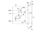
図1は本実施形態における固体撮像装置のブロック図である。固体撮像装置は、例えばCMOS(Complementary Metal Oxide Semiconductor)イメージセンサであって、画素部1、垂直走査回路2、列回路3、水平走査回路4、出力回路5、制御回路6、列信号線11、電流源13を備える。
[First Embodiment]
FIG. 1 is a block diagram of a solid-state image sensor according to the present embodiment. The solid-state image sensor is, for example, a CMOS (Complementary Metal Oxide Sensor) image sensor, which includes a pixel unit 1, a vertical scanning circuit 2, a row circuit 3, a
画素部1は行列状に配列された複数の画素10を備え、それぞれの画素10は照射光に基づき信号電荷を生成および蓄積する光電変換部を備える。なお、本明細書において、行方向とは図面における水平方向を示し、列方向とは図面において垂直方向を示すものとする。画素10上にはマイクロレンズ、カラーフィルタが配置され得る。カラーフィルタは例えば赤、青、緑の原色フィルタであって、ベイヤー配列に従って各画素10に設けられている。一部の画素10はOB画素(オプティカル・ブラック画素)として遮光されている。複数の画素10には、焦点検出用の画素信号を出力する焦点検出画素が配された測距行と、画像を生成するための画素信号を出力する撮像画素が配された複数の撮像行とが設けられ得る。列信号線11は画素10の列毎に設けられ、列信号線11には電流源13が電気的に接続される。本実施形態においては、列信号線11毎にフィードバック回路15が設けられているが、複数の画素10を含む画素群毎にフィードバック回路15が設けられても良い。フィードバック回路15は列信号線11における信号電圧に応じた電圧を電圧供給線105を介して各列の複数の画素10に供給している。
The pixel unit 1 includes a plurality of
垂直走査回路2はシフトレジスタ、ゲート回路、バッファ回路などから構成され、垂直同期信号、水平同期信号、クロック信号などに基づき行毎に駆動パルスを選択的に画素10に出力する。駆動パルスは、行ごと、順次、もしくはランダムに供給され得る。列回路3は列信号線11毎の信号処理回路30を備える。信号処理回路30は差動増幅回路、保持回路を備え、画素10から列信号線11に出力された画素信号を増幅するとともに、一時的に保持する。信号処理回路30は画素10のリセット時の画素信号と光電変換時の画素信号との差分を算出することにより、相関二重サンプリングを行うことができる。
The vertical scanning circuit 2 is composed of a shift register, a gate circuit, a buffer circuit, and the like, and selectively outputs a drive pulse for each row to the
水平走査回路4はシフトレジスタを備え、信号処理回路30に保持された画素信号を順に読み出す。出力回路5は差動増幅回路、バッファ回路、クランプ回路を備え、水平走査回路4から読み出された画素信号を固体撮像装置の外部へと出力する。このような構成により、光学系を介して画素部1上に照射された光を電気信号である二次元の画像信号として出力させることができる。なお、出力回路5にアナログ・デジタル変換回路を設け、デジタルの画像信号を出力しても良い。または、列毎にアナログ・デジタル変換回路を設けても良い。制御回路6は、クロック、同期信号などに基づき様々な制御信号、駆動信号を生成するタイミングジェネレータとして機能する。
The
図2は本実施形態における画素10の等価回路図である。画素10は、光電変換部PD、転送トランジスタM1、浮遊拡散領域FD(Floating Diffusion)、リセットトランジスタM2、増幅トランジスタM3、選択トランジスタM4を含む。以下の説明は、画素10を構成するトランジスタがNチャネルMOSトランジスタである例を示している。光電変換部PDは例えばフォトダイオードから構成されており、入射光による光電変換および電荷の蓄積を行なう。なお、光電変換部PDはフォトダイオードに限定されず、光電効果を生じさせる材料であれば良い。さらに、埋め込み型のフォトダイオードを構成することで、暗電流ノイズを低減できる。光電変換部PDにはマイクロレンズが設けられており、マイクロレンズにより集光された光が光電変換部PDに入射する。
FIG. 2 is an equivalent circuit diagram of the
転送トランジスタM1は光電変換部PDに対応して設けられ、ゲートには垂直走査回路2から駆動パルスPTXが印加される。駆動パルスPTXがハイレベルとなると、転送トランジスタM1がオン状態(導通状態)となり、光電変換部PDに蓄積された信号電荷が増幅トランジスタM3のゲート(第1の入力ノード)に形成された浮遊拡散領域FDに転送される。また、駆動パルスPTXがローレベルとなると、転送トランジスタM1はオフ状態(非導通状態)となる。転送トランジスタM1をオンまたはオフすることにより、光電変換部PDの信号電荷を浮遊拡散領域FDに転送することができる。浮遊拡散領域FDは信号電荷を電圧に変換し、増幅トランジスタM3はゲート電圧に応じた信号電圧をソース(第1の主ノード)から選択トランジスタM4を介して列信号線11へ出力する。
The transfer transistor M1 is provided corresponding to the photoelectric conversion unit PD, and a drive pulse PTX is applied to the gate from the vertical scanning circuit 2. When the drive pulse PTX reaches a high level, the transfer transistor M1 is turned on (conducting state), and the signal charge accumulated in the photoelectric conversion unit PD is suspended and diffused formed at the gate (first input node) of the amplification transistor M3. Transferred to region FD. Further, when the drive pulse PTX becomes low level, the transfer transistor M1 is turned off (non-conducting state). By turning on or off the transfer transistor M1, the signal charge of the photoelectric conversion unit PD can be transferred to the floating diffusion region FD. The stray diffusion region FD converts the signal charge into a voltage, and the amplification transistor M3 outputs a signal voltage corresponding to the gate voltage from the source (first main node) to the
リセットトランジスタM2のソースは浮遊拡散領域FDに接続され、ゲートには垂直走査回路2から駆動パルスPRESが印加される。駆動パルスPRESがハイレベルとなると、リセットトランジスタM2はオン状態となり、浮遊拡散領域FDにリセット電圧VRESが供給される。選択トランジスタM4は増幅トランジスタM3と列信号線11との間に設けられており、選択トランジスタM4のゲートには垂直走査回路2から駆動パルスPSELが印加される。駆動パルスPSELがハイレベルとなると、増幅トランジスタM3と列信号線11とが電気的に導通する。列信号線11には電流源13が電気的に接続されている。電流源13はMOSトランジスタから構成され、ドレインは列信号線11に電気的に接続され、ソースはグランド配線に電気的に接続される。電流源13のゲートには所定の電位が印加され、電流源13は列信号線11を介して増幅トランジスタM3のソースに一定のバイアス電流を供給する。
The source of the reset transistor M2 is connected to the floating diffusion region FD, and a drive pulse PRESS is applied to the gate from the vertical scanning circuit 2. When the drive pulse PRESS becomes high level, the reset transistor M2 is turned on and the reset voltage VRES is supplied to the floating diffusion region FD. The selection transistor M4 is provided between the amplification transistor M3 and the
フィードバック回路15は、本実施形態においては列信号線11毎に設けられ、増幅トランジスタM3から出力された信号電圧に追従して変化する電圧を増幅トランジスタM3のドレイン(第2の主ノード)に供給する。フィードバック回路15は、一例として、NチャネルMOSのフィードバック用トランジスタ15aから構成され、フィードバック用トランジスタ15aの極性は増幅トランジスタM3の極性と同じであり得る。フィードバック用トランジスタ15aにおいて、ゲート(第2の入力ノード)は列信号線11に接続され、ドレイン(第3の主ノード)は電源電圧VDDの電源配線に接続され、ソース(第4の主ノード)は電圧供給線105を介して増幅トランジスタM3のドレインに接続される。このように、フィードバック用トランジスタ15aは電源配線と増幅トランジスタM3のドレインとの間に直列に接続される。選択トランジスタM4がオン状態である場合、電流源13から増幅トランジスタM3に駆動電流が供給され、フィードバック用トランジスタ15aは増幅トランジスタM3に供給された駆動電流のみによってソースフォロワとして動作する。ここで、「駆動電流のみによって」は、実質的に解釈されるべきであって、漏れ電流などのように半導体設計上、回避し得ない電流分を排除する趣旨ではない。
The
ここで、フィードバック用トランジスタ15aの閾値電圧をVth1とすると、フィードバック用トランジスタ15aのソース電圧、すなわち増幅トランジスタM3のドレイン電圧VDは、列信号線11の信号電圧よりも電圧ΔV1および閾値電圧Vth1だけ低くなる。よって、ドレイン電圧VDは式1で表される。電圧V0は列信号線11の信号電圧であり、電圧ΔV1は電流源13から供給される電流値およびコンダクタンスによって定まる電圧である。
VD=V0−Vth1−ΔV1 (式1)
Here, assuming that the threshold voltage of the
VD = V0-Vth1-ΔV1 (Equation 1)
一方、増幅トランジスタM3がソースフォロワとして動作する場合、増幅トランジスタM3のゲート電圧VGおよびドレイン電圧VDは一定の電圧差を保ちながら変化する。このため、増幅トランジスタM3のゲート・ドレイン間の容量は実質的にゼロ、若しくは極めて低い値となる。さらに、増幅トランジスタM3のソース・ドレイン間の電圧は信号電圧の大きさによらず一定であるため、チャンネル長変調効果が抑制され、ソースフォロワの出力ゲインを高くすることが可能となる。 On the other hand, when the amplification transistor M3 operates as a source follower, the gate voltage VG and the drain voltage VD of the amplification transistor M3 change while maintaining a constant voltage difference. Therefore, the capacitance between the gate and drain of the amplification transistor M3 is substantially zero or extremely low. Further, since the voltage between the source and drain of the amplification transistor M3 is constant regardless of the magnitude of the signal voltage, the channel length modulation effect is suppressed, and the output gain of the source follower can be increased.
また、増幅トランジスタM3の閾値電圧をVth2、ドレイン電圧をVD、ゲート電圧をVGとした場合、増幅トランジスタM3がソースフォロワとして動作するためには以下の式2の条件を満たせば良い。
VD≧VG−Vth2 (式2)
Further, when the threshold voltage of the amplification transistor M3 is Vth2, the drain voltage is VD, and the gate voltage is VG, the condition of the following equation 2 may be satisfied in order for the amplification transistor M3 to operate as a source follower.
VD ≧ VG-Vth2 (Equation 2)
さらに、列信号線11の信号電圧V0は、以下の式3によって表される。
V0=VG−Vth2−ΔV2 (式3)
Further, the signal voltage V0 of the
V0 = VG-Vth2-ΔV2 (Equation 3)
ここで、ΔV2は、電流源13から供給される電流値と増幅トランジスタM3のコンダクタンスと選択トランジスタM4のオン抵抗とによって定まる電圧である。式1および式3から以下の式4が導かれる。
VD=VG−Vth2−ΔV2−Vth1−ΔV1 (式4)
Here, ΔV2 is a voltage determined by the current value supplied from the
VD = VG-Vth2-ΔV2-Vth1-ΔV1 (Equation 4)
よって、ソースフォロワ動作条件に関する式2を式4に代入することにより以下の式5が導かれる。
VG−Vth2−ΔV2−Vth1−ΔV1≧VG−Vth2 (式5)
Therefore, the following equation 5 is derived by substituting the equation 2 relating to the source follower operating conditions into the
VG-Vth2-ΔV2-Vth1-ΔV1 ≧ VG-Vth2 (Equation 5)
式5を整理し、以下の式6が導かれる。
−ΔV2−ΔV1≧Vth1 (式6)
Equation 5 is rearranged and the
−ΔV2-ΔV1 ≧ Vth1 (Equation 6)
ΔV1、ΔV2はともに正の値なので閾値電圧Vth1は負の値となる。増幅トランジスタM3がソースフォロワとして動作するために、フィードバック用トランジスタ15aはデプレッション型であって、式6の閾値電圧Vth1を有することが好ましい。
Since both ΔV1 and ΔV2 are positive values, the threshold voltage Vth1 has a negative value. In order for the amplification transistor M3 to operate as a source follower, it is preferable that the
電圧V0がフィードバック用トランジスタ15aのゲート電圧であることから、フィードバック用トランジスタ15aがソースフォロワ動作するため、以下の式7を満たすことが好ましい。
VDD≧V0−Vth1 (式7)
Since the voltage V0 is the gate voltage of the
VDD ≧ V0-Vth1 (Equation 7)
式7および式3から式8が導かれる。
VDD≧VG−Vth2−ΔV2−Vth1 (式8)
Equation 8 is derived from
VDD ≧ VG-Vth2-ΔV2-Vth1 (Equation 8)
式8はさらに式9で表される。
VG≦VDD+Vth2+Vth1+ΔV2 (式9)
Equation 8 is further represented by Equation 9.
VG ≤ VDD + Vth2 + Vth1 + ΔV2 (Equation 9)
増幅トランジスタM3のゲート電圧VGはリセット電圧VRESにリセットされることから、式9は式10で表される。
VRES≦VDD+Vth2+Vth1+ΔV2 (式10)
Since the gate voltage VG of the amplification transistor M3 is reset to the reset voltage VRES, the equation 9 is represented by the
VRES ≤ VDD + Vth2 + Vth1 + ΔV2 (Equation 10)
以上により、式6および式10が満たされることで、増幅トランジスタM3はソースフォロワとして動作する。なお、式10において、閾値電圧Vth1、Vth2の値によっては、リセット電圧VRESは電源電圧VDDよりも低く設定されることが好ましい。
As described above, when the
上述のように構成された固体撮像装置の概略の動作を説明する。垂直走査回路2は駆動パルスPRESをハイレベルとすることで、浮遊拡散領域FDの電荷をリセットする。垂直走査回路2は駆動パルスPRESをローレベルとし、リセット動作を終了する。列信号線11には、画素10のリセット状態における信号電圧が出力され、信号処理回路30の容量に保持される。次に、垂直走査回路2は駆動パルスPTXをハイレベルとした後にローレベルとし、光電変換部PDに蓄積された信号電荷を浮遊拡散領域FDに転送する。浮遊拡散領域FDの電位は、電荷量に応じて所定電位だけ低くなる。増幅トランジスタM3からは、浮遊拡散領域FDの信号電荷に基づく信号電圧が列信号線11に出力される。フィードバック用トランジスタ15aのゲートには列信号線11における信号電圧が入力され、フィードバック用トランジスタ15aのソースの電位は信号電圧に追従して所定電位だけ低くなる。上述したように、増幅トランジスタM3がソースフォロワとして動作する場合、増幅トランジスタM3のゲート電圧およびドレイン電圧は一定の電圧差を保ちながら変化する。増幅トランジスタM3のソースから光電変換時の信号電圧が列信号線11に出力され、信号処理回路30の容量に保持される。信号処理回路30のコンパレータ回路はリセット情報における信号電圧と光電変換時の信号電圧の差分の信号を出力することで、ノイズ成分が除去された信号を得ることができる。
The schematic operation of the solid-state image sensor configured as described above will be described. The vertical scanning circuit 2 resets the charge in the floating diffusion region FD by setting the drive pulse PRES to a high level. The vertical scanning circuit 2 sets the drive pulse PRES to a low level and ends the reset operation. The signal voltage in the reset state of the
以上、述べたように、本実施形態によれば、フィードバック回路15は、増幅トランジスタM3の信号電圧に追従して変化する電圧を増幅トランジスタM3の第2のドレインに供給する。増幅トランジスタM3のゲート・ドレイン間の容量を実質的に無くし、若しくは極めて小さくすることができるとともに、チャネル長変調効果を抑制することができる。これにより、出力ゲインを高くし、信号対雑音比を向上させることができる。また、フィードバック回路15は増幅トランジスタM3の駆動電流のみによって動作するため、消費電流の増加を抑制しながら、信号対雑音比を高めることが可能となる。
As described above, according to the present embodiment, the
[第2実施形態]
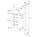
続いて、本発明の第2実施形態における固体撮像装置について、第1実施形態と異なる構成を中心に説明する。図3は本実施形態における画素10の等価回路図である。本実施形態において、フィードバック回路15は画素10毎に設けられている。画素10において、1つのフィードバック用トランジスタ15aが1つの増幅トランジスタM3に対応して設けられ、フィードバック用トランジスタ15aのソースは電圧供給線105を介して増幅トランジスタM3のドレインにのみ接続されている。フィードバック用トランジスタ15aのゲートは配線103を介して増幅トランジスタM3のソースに接続される。
[Second Embodiment]
Subsequently, the solid-state image sensor according to the second embodiment of the present invention will be described focusing on a configuration different from that of the first embodiment. FIG. 3 is an equivalent circuit diagram of the
本実施形態においても、フィードバック用トランジスタ15aは、増幅トランジスタM3のソースから出力された信号電圧に追従して変化する電圧を増幅トランジスタM3のドレインに供給する。これにより、増幅トランジスタM3のゲート・ドレイン間の容量を実質的に無くし、若しくは極めて小さくすることができ、信号対雑音比を高めることができる。また、フィードバック用トランジスタ15aは増幅トランジスタM3の駆動電流のみによって動作するため、消費電流の増加を抑制することができる。
Also in this embodiment, the
さらに、本実施形態においては、フィードバック用トランジスタ15aは画素10毎に設けられ、フィードバック用トランジスタ15aからの電圧供給線105には1つの増幅トランジスタM3のドレインが接続されている。このため、第1実施形態と比較して、電圧供給線105における容量を小さくすることができ、フィードバックの遅延時間を大幅に低減することが可能となる。
Further, in the present embodiment, the
また、本実施形態においては、フィードバックされる信号電圧は、列信号線11の信号電圧ではなく、増幅トランジスタM3のソースの信号電圧である。このため、上述の式6(−ΔV2−ΔV1≧Vth1)において、ΔV2の値は、第1実施形態におけるΔV2と比較して、選択トランジスタM4のオン抵抗による電圧降下分だけ小さくなる。したがって、フィードバック用トランジスタ15aの閾値電圧Vth1が満たすべき条件は第1実施形態に比較して緩和され、設計の自由度を高めることができる。
Further, in the present embodiment, the signal voltage fed back is not the signal voltage of the
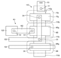
図4は本実施形態における画素の平面図である。図4において、図3における回路要素に対応する構成には同一の参照符号が付されている。アクティブ領域110、120には薄いゲート酸化膜が形成され、アクティブ領域110、120以外の領域には厚い酸化膜が付された素子分離領域が形成されている。
FIG. 4 is a plan view of the pixels in this embodiment. In FIG. 4, the same reference numerals are given to the configurations corresponding to the circuit elements in FIG. A thin gate oxide film is formed in the
アクティブ領域120には転送トランジスタM1のソース領域が形成され、ソース領域は光電変換部PDから転送された信号電荷を保持する浮遊拡散領域FDを構成する。浮遊拡散領域FDにはコンタクトホールC2を介して配線102の一端に接続される。配線102の他端はコンタクトホールC3を介して増幅トランジスタM3のゲート電極M3gに接続される。
A source region of the transfer transistor M1 is formed in the
アクティブ領域110において、増幅トランジスタM3のゲート電極M3gは領域110bと領域110cとの間のチャネル領域上に絶縁層を介して形成される。領域110cは増幅トランジスタM3のソース領域および選択トランジスタM4のドレイン領域を兼ねている。領域110cと領域110dとの間のチャネル領域上には絶縁層を介して選択トランジスタM4のゲート電極M4gが形成される。ゲート電極M4gはコンタクトホールC6を介して駆動配線104に接続される。領域110dは選択トランジスタM4のソース領域を構成し、図示されていない列信号線11に接続される。さらに、アクティブ領域110において、領域110aと領域110bとの間のチャネル領域上には、絶縁層を介してフィードバック用トランジスタ15aのゲート電極15gが形成される。ゲート電極15gはコンタクトホールC4を介して配線103に接続されている。配線103はさらにコンタクトホールC5を介して領域110c、すなわち増幅トランジスタM3のソース領域および選択トランジスタM4のドレイン領域に接続されている。領域110aはフィードバック用トランジスタ15aのドレイン領域を構成し、領域110aはコンタクトホールC1を介して電源配線101に接続される。領域110bはフィードバック用トランジスタ15aのソース領域および増幅トランジスタM3のドレイン領域を兼ねている。
In the
図4において、配線(第1の配線)103は増幅トランジスタM3のゲート電極M3gと交差するとともに、配線(第2の配線)102および浮遊拡散領域FDに隣接している。しかし、配線103と、ゲート電極M3g、配線102、浮遊拡散領域FDとの間の容量は、配線103が増幅トランジスタM3の出力であるから実質的に無くなり、若しくは極めて小さくなる。また、配線102と駆動配線(第3の配線)104との間に配線103の少なくとも一部が平面視において位置することにより、駆動配線104と配線102との間の容量は電気的遮蔽効果によって低減される。選択トランジスタM4の駆動配線104と同様に、転送トランジスタM1の駆動配線およびリセットトランジスタM2の駆動配線についても配線102との容量を低減することが可能である。さらに、図示されていないが、配線103に接続される上層の配線を浮遊拡散領域FD、配線102の大部分を覆うように配置してもよい。これにより、浮遊拡散領域FD、配線102、ゲート電極M3gと駆動配線、電源配線101等との間の容量を電気的遮蔽効果によって低減できる。
In FIG. 4, the wiring (first wiring) 103 intersects with the gate electrode M3g of the amplification transistor M3 and is adjacent to the wiring (second wiring) 102 and the stray diffusion region FD. However, the capacitance between the
以上説明したように、本実施形態によれば、消費電流の増加を抑制しながら、信号対雑音比を高めることが可能となる。また、フィードバック回路15が画素10毎に設けられているため、第1実施形態と比較して、電圧供給線105における容量を小さくすることができ、フィードバックの遅延時間を大幅に低減することが可能となる。
As described above, according to the present embodiment, it is possible to increase the signal-to-noise ratio while suppressing the increase in current consumption. Further, since the
[第3実施形態]
続いて、本発明の第3実施形態における固体撮像装置について、第2実施形態と異なる構成を中心に説明する。図5は本実施形態における画素10の等価回路図である。本実施形態において、画素10は転送トランジスタM1を備えておらず、光電変換部PDのN電極は浮遊拡散領域FDを構成している。このような構成の画素10においては、第1、第2実施形態と異なり、相関二重サンプリングによるノイズ除去を行うことができない。この場合、増幅トランジスタM3の信号電圧をリセット電圧VRESにフィードバックする回路を設けても良い。
[Third Embodiment]
Subsequently, the solid-state image sensor according to the third embodiment of the present invention will be described focusing on a configuration different from that of the second embodiment. FIG. 5 is an equivalent circuit diagram of the
本実施形態においても、増幅トランジスタM3がソースフォロワとして動作するための駆動電流のみによって動作するフィードバック回路を用いることにより、消費電流の増加を抑制しながら、信号対雑音比を高めることが可能となる。 Also in this embodiment, by using a feedback circuit that operates only by the drive current for the amplification transistor M3 to operate as a source follower, it is possible to increase the signal-to-noise ratio while suppressing an increase in current consumption. ..
[第4実施形態]
続いて、本発明の第4実施形態における固体撮像装置について、第1実施形態と異なる構成を中心に説明する。図6は本実施形態における画素10の等価回路図である。画素10は、光電変換部PDA、PDB、転送トランジスタM1A、M1B、浮遊拡散領域FD、リセットトランジスタM2、増幅トランジスタM3、選択トランジスタM4を含む。光電変換部PDA、PDBは例えばフォトダイオードから構成されており、入射光による光電変換および電荷の蓄積を行なう。光電変換部PDA、PDBには共通のマイクロレンズが設けられており、マイクロレンズにより集光された光が光電変換部PDA、PDBに入射する。このように、2つの光電変換部PDA、PDBは瞳分割されている。なお、画素10を構成する光電変換部の個数は2個に限定されず、それ以上の個数であっても良い。
[Fourth Embodiment]
Subsequently, the solid-state image sensor according to the fourth embodiment of the present invention will be described focusing on a configuration different from that of the first embodiment. FIG. 6 is an equivalent circuit diagram of the
転送トランジスタM1A、M1Bは光電変換部PDA、PDBに対応して設けられ、それぞれのゲートには駆動パルスPTXA、PTXBが印加される。駆動パルスPTXA、PTXBがハイレベルとなると、転送トランジスタM1A、M1Bがオン状態(導通状態)となり、光電変換部PDA、PDBの信号が増幅トランジスタM3の入力ノードである浮遊拡散領域FDに転送される。また、駆動パルスPTXA、PTXBがローレベルとなると、転送トランジスタM1A、M1Bはオフ状態(非導通状態)となる。転送トランジスタM1A、M1Bを同時にオンまたはオフすることにより、光電変換部PDA、PDBの信号電荷を浮遊拡散領域FDに転送することができる。増幅トランジスタM3は、浮遊拡散領域FDにおいて加算された信号電荷に応じた信号電圧をソースから出力する。また、駆動パルスPTXAをオンまたはオフすることにより、光電変換部PDAの信号電荷が浮遊拡散領域FDに転送され、増幅トランジスタM3は信号電荷に応じた信号電圧をソースから出力する。以上の構成により、光電変換部PDA、PDBのそれぞれの信号電荷を加算した(A+B)信号、光電変換部PDAのA信号を得ることができる。(A+B)信号は画像信号として用いられる。光電変換部PDBのB信号は(A+B)信号からA信号を減算することで求められる。なお、減算を行わずに、光電変換部PDBからの信号電荷を独立に読み出しても良い。A信号、B信号は位相差検出のための焦点検出信号として用いられる。 The transfer transistors M1A and M1B are provided corresponding to the photoelectric conversion units PDA and PDB, and drive pulses PTXA and PTXB are applied to the respective gates. When the drive pulses PTXA and PTXB reach a high level, the transfer transistors M1A and M1B are turned on (conducting state), and the signals of the photoelectric conversion units PDA and PDB are transferred to the floating diffusion region FD which is the input node of the amplification transistor M3. .. Further, when the drive pulses PTXA and PTXB become low level, the transfer transistors M1A and M1B are turned off (non-conducting state). By turning on or off the transfer transistors M1A and M1B at the same time, the signal charges of the photoelectric conversion units PDA and PDB can be transferred to the floating diffusion region FD. The amplification transistor M3 outputs a signal voltage corresponding to the signal charge added in the stray diffusion region FD from the source. Further, by turning on or off the drive pulse PTXA, the signal charge of the photoelectric conversion unit PDA is transferred to the floating diffusion region FD, and the amplification transistor M3 outputs a signal voltage corresponding to the signal charge from the source. With the above configuration, it is possible to obtain a (A + B) signal obtained by adding the signal charges of the photoelectric conversion units PDA and PDB, and an A signal of the photoelectric conversion unit PDA. The (A + B) signal is used as an image signal. The B signal of the photoelectric conversion unit PDB is obtained by subtracting the A signal from the (A + B) signal. The signal charge from the photoelectric conversion unit PDB may be read independently without subtraction. The A signal and the B signal are used as focus detection signals for phase difference detection.
フィードバック回路15は第1実施形態と同様に列信号線11毎に設けられ、増幅トランジスタM3から出力された信号電圧に追従して変化する電圧を電圧供給線105を介して増幅トランジスタM3のドレインに供給する。また、フィードバック用トランジスタ15aは電源電圧VDDの電源配線と増幅トランジスタM3のドレインとの間に直列に接続され、フィードバック用トランジスタ15aは増幅トランジスタM3に供給された駆動電流のみでソースフォロワとして動作する。
The
本実施形態においても、瞳分割の画素10における浮遊拡散領域FDの容量を実質的に無くし、若しくは極めて小さくし、信号ゲインを大きくすることができる。また、フィードバック回路は増幅トランジスタの駆動電流のみによって動作するため、消費電流の増加を抑制しながら、信号対雑音比を高めることが可能となる。
Also in this embodiment, the capacitance of the floating diffusion region FD in the
[第5実施形態]
続いて、本発明の第5実施形態における固体撮像装置について、第4実施形態と異なる構成を中心に説明する。図7は本実施形態における画素10の等価回路図である。フィードバック回路15は画素10毎に設けられている。画素10において、1つのフィードバック用トランジスタ15aが1つの増幅トランジスタM3に対応して設けられ、フィードバック用トランジスタ15aのソースは電圧供給線105を介して増幅トランジスタM3のドレインにのみ接続されている。本実施形態においても、瞳分割の画素10における浮遊拡散領域FDの容量を実質的に無くし、若しくは極めて小さくし、信号電圧の出力ゲインを大きくすることができる。また、フィードバック回路は増幅トランジスタの駆動電流のみによって動作するため、消費電流の増加を抑制しながら、信号対雑音比を高めることが可能となる。
[Fifth Embodiment]
Subsequently, the solid-state image sensor according to the fifth embodiment of the present invention will be described focusing on a configuration different from that of the fourth embodiment. FIG. 7 is an equivalent circuit diagram of the
[第6実施形態]
上述の実施形態における固体撮像装置は種々の撮像システムに適用可能である。撮像システムとして、デジタルスチルカメラ、デジタルカムコーダ、カメラヘッド、複写機、ファックス、携帯電話、車載カメラ、観測衛星、監視カメラなどがあげられる。図8に、撮像システムの例としてデジタルスチルカメラのブロック図を示す。
[Sixth Embodiment]
The solid-state image sensor in the above-described embodiment can be applied to various image pickup systems. Examples of the imaging system include a digital still camera, a digital camcorder, a camera head, a copier, a fax machine, a mobile phone, an in-vehicle camera, an observation satellite, and a surveillance camera. FIG. 8 shows a block diagram of a digital still camera as an example of an imaging system.
図8に示す撮像システムは、バリア206、レンズ202、絞り204、撮像装置207、信号処理部208、タイミング発生部220、全体制御・演算部218、メモリ部210、記録媒体制御I/F部216、記録媒体214、外部I/F部212を含む。バリア206はレンズ202を保護し、レンズ202は被写体の光学像を撮像装置207に結像させる。絞り204はレンズ202を通った光量を可変する。撮像装置207は上述の実施形態の固体撮像装置を含み、レンズ202により結像された光学像を画像データに変換する。ここで、撮像装置207の半導体基板にはAD変換部が形成されているものとする。信号処理部208は撮像装置207より出力された撮像データに各種の補正やデータを圧縮する。タイミング発生部220は撮像装置207および信号処理部208に、各種タイミング信号を出力する。全体制御・演算部218はデジタルスチルカメラ全体を制御し、メモリ部210は画像データを一時的に記憶する。記録媒体制御I/F部216は記録媒体214に画像データの記録または読み出しを行うためのインターフェースであり、記録媒体214は撮像データの記録または読み出しを行うための半導体メモリ等の着脱可能な記録媒体である。外部I/F部212は外部コンピュータ等と通信するためのインターフェースである。タイミング信号などは撮像システムの外部から入力されてもよく、撮像システムは少なくとも撮像装置207と、撮像装置207から出力された撮像信号を処理する信号処理部208とを有すればよい。
The imaging system shown in FIG. 8 includes a
本実施形態では、撮像装置207とAD変換部とが別の半導体基板に設けられた構成を説明した。しかし、撮像装置207とAD変換部とが同一の半導体基板に形成されていてもよい。また、撮像装置207と信号処理部208とが同一の半導体基板に形成されていてもよい。
In the present embodiment, the configuration in which the
また、それぞれの画素が第1の光電変換部と、第2の光電変換部を含んでもよい。信号処理部208は、第1の光電変換部で生じた電荷に基づく画素信号と、第2の光電変換部で生じた電荷に基づく画素信号とを処理し、撮像装置207から被写体までの距離情報を取得するように構成されてもよい。
Further, each pixel may include a first photoelectric conversion unit and a second photoelectric conversion unit. The
[第7実施形態]
図9(a)、図9(b)は、本発明の第7実施形態における車載カメラに関する撮像システムの一例を示したものである。撮像システム300は、上述した実施形態の撮像装置310を有する。撮像システム300は、撮像装置310により取得された複数の画像データに対し、画像処理を行う画像処理部312と、撮像システム300より取得された複数の画像データから視差(視差画像の位相差)の算出を行う視差取得部314を有する。また、撮像システム300は、算出された視差に基づいて対象物までの距離を算出する距離取得部316と、算出された距離に基づいて衝突可能性があるか否かを判定する衝突判定部318とを有する。ここで、視差取得部314、距離取得部316は、対象物までの距離情報を取得する距離情報取得手段の一例である。すなわち、距離情報とは、視差、デフォーカス量、対象物までの距離等に関する情報である。衝突判定部318はこれらの距離情報のいずれかを用いて、衝突可能性を判定してもよい。距離情報取得手段は、専用に設計されたハードウェアによって実現されてもよいし、ソフトウェアモジュールによって実現されてもよい。また、FPGA(Field Programmable Gate Array)、ASIC(Application Specific Integrated Circuit)によって実現されてもよいし、これらの組合せによって実現されてもよい。
[7th Embodiment]
9 (a) and 9 (b) show an example of an imaging system relating to an in-vehicle camera according to a seventh embodiment of the present invention. The
撮像システム300は車両情報取得装置320と接続されており、車速、ヨーレート、舵角などの車両情報を取得することができる。また、撮像システム300は、衝突判定部318での判定結果に基づいて、車両に対して制動力を発生させる制御信号を出力する制御装置である制御ECU330が接続されている。また、撮像システム300は、衝突判定部318での判定結果に基づいて、ドライバーへ警報を発する警報装置340とも接続されている。例えば、衝突判定部318の判定結果として衝突可能性が高い場合、制御ECU330はブレーキをかける、アクセルを戻す、エンジン出力を抑制するなどして衝突を回避、被害を軽減する車両制御を行う。警報装置340は音等の警報を鳴らす、カーナビゲーションシステムなどの画面に警報情報を表示する、シートベルトやステアリングに振動を与えるなどしてユーザに警告を行う。撮像システム300は上述のように車両を制御する動作の制御を行う制御手段として機能する。
The
本実施形態では車両の周囲、例えば前方または後方を撮像システム300で撮像する。図9(b)に、車両前方(撮像範囲350)を撮像する場合の撮像システムを示した。撮像制御手段としての車両情報取得装置320が、上述の第1乃至第6の実施形態に記載した動作を行うように撮像システム300ないしは撮像装置310に指示を送る。撮像装置310の動作は、第1乃至第6の実施形態と同じなので、ここでは説明を省略する。このような構成により、測距の精度をより向上させることができる。
In the present embodiment, the surroundings of the vehicle, for example, the front or the rear, are imaged by the
上述では、他の車両と衝突しないように制御する例を説明したが、他の車両に追従して自動運転する制御、車線からはみ出さないように自動運転する制御などにも適用可能である。さらに、撮像システムは、自車両等の車両に限らず、例えば、船舶、航空機あるいは産業用ロボットなどの移動体(移動装置)に適用することができる。加えて、移動体に限らず、高度道路交通システム(ITS)等、広く物体認識を利用する機器に適用することができる。 In the above description, an example of controlling so as not to collide with another vehicle has been described, but it can also be applied to control for automatically driving following another vehicle, control for automatically driving so as not to go out of the lane, and the like. Further, the imaging system can be applied not only to a vehicle such as a own vehicle but also to a moving body (moving device) such as a ship, an aircraft, or an industrial robot. In addition, it can be applied not only to mobile objects but also to devices that widely use object recognition, such as intelligent transportation systems (ITS).
[他の実施形態]
本発明は、上述の実施形態に限らず種々の変形が可能である。例えば、いずれかの実施形態の一部の構成を他の実施形態に追加した例や、他の実施形態の一部の構成と置換した例も、本発明の実施形態である。
[Other Embodiments]
The present invention is not limited to the above-described embodiment, and various modifications can be made. For example, an example in which a part of the configuration of any of the embodiments is added to another embodiment or an example in which a part of the configuration of another embodiment is replaced with another embodiment is also an embodiment of the present invention.
上述の実施形態においては、1つの画素が1つの増幅トランジスタを備えた構成を説明したが、本発明はこれらの構成に限定されない。例えば、1つの画素が複数の光電変換部に対応して複数の増幅トランジスタを備えている場合、フィードバックトランジスタを増幅トランジスタ毎に設けても良い。 In the above-described embodiment, the configuration in which one pixel includes one amplification transistor has been described, but the present invention is not limited to these configurations. For example, when one pixel is provided with a plurality of amplification transistors corresponding to a plurality of photoelectric conversion units, a feedback transistor may be provided for each amplification transistor.
上述の実施形態では、トランジスタをN型トランジスタにより構成する場合を想定して説明を行ったが、トランジスタをP型トランジスタにより構成するようにしてもよい。この場合、上述した各駆動信号のレベルは逆になる。 In the above-described embodiment, the description has been made on the assumption that the transistor is composed of an N-type transistor, but the transistor may be composed of a P-type transistor. In this case, the levels of the above-mentioned drive signals are reversed.
なお、上述の実施形態は、いずれも本発明を実施するにあたっての具体化の例を示したものに過ぎず、これらによって本発明の技術的範囲が限定的に解釈されてはならない。すなわち、本発明はその技術思想、またはその主要な特徴から逸脱することなく、様々な形で実施することができる。 It should be noted that the above-described embodiments are merely examples of embodiment in carrying out the present invention, and the technical scope of the present invention should not be construed in a limited manner by these. That is, the present invention can be implemented in various forms without departing from the technical idea or its main features.
1 画素部
2 垂直走査回路
3 列回路
4 水平走査回路
5 出力回路
6 制御回路
10 画素
11 列信号線
13 電流源
15 フィードバック回路
102 配線(第2の配線)
103 配線(第1の配線)
104 配線(第3の配線)
PD 光電変換回路
FD 浮遊拡散領域
M3 増幅トランジスタ
M4 選択トランジスタ
1 Pixel part 2 Vertical scanning circuit 3
103 wiring (first wiring)
104 wiring (third wiring)
PD photoelectric conversion circuit FD Floating diffusion region M3 amplification transistor M4 selection transistor
Claims (28)
第2の入力ノードと、第3の主ノードと、第4の主ノードとを備え、前記増幅トランジスタと同じ極性の第1のトランジスタと、
前記複数の画素の各々の前記第1の主ノードが電気的に接続される信号線と、
前記信号線に電気的に接続される電流源と、
前記複数の画素を各々が含む複数の画素群と、
を有し、
前記第3の主ノードには電源電圧が与えられ、
前記第4の主ノードと、前記第2の主ノードとが電気的に接続され、
前記第1の主ノードと前記第2の入力ノードとが電気的に接続され、
前記複数の画素群のそれぞれに対応して、複数の前記信号線の各々が対応して設けられ、
前記第1のトランジスタが、複数の前記信号線の各々に対応して設けられていることを特徴とする固体撮像装置。 A plurality of pixels each having a photoelectric conversion unit and an amplification transistor including a first input node, a first main node, and a second main node electrically connected to the photoelectric conversion unit.
A first transistor having a second input node, a third main node, and a fourth main node and having the same polarity as the amplification transistor.
A signal line to which the first main node of each of the plurality of pixels is electrically connected, and
With a current source electrically connected to the signal line,
A plurality of pixel groups, each of which includes the plurality of pixels,
Have,
A power supply voltage is applied to the third main node.
The fourth main node and the second main node are electrically connected to each other.
The first main node and the second input node are electrically connected to each other.
Each of the plurality of signal lines is provided corresponding to each of the plurality of pixel groups.
A solid-state image sensor, wherein the first transistor is provided corresponding to each of the plurality of signal lines.
第2の入力ノードと、第3の主ノードと、第4の主ノードとを備え、前記増幅トランジスタと同じ極性の第1のトランジスタと、
前記複数の画素の各々の前記第1の主ノードが電気的に接続される信号線と、
前記信号線に電気的に接続される電流源とを有し、
前記電流源が供給する駆動電流によって動作するフィードバック回路を有し、
前記フィードバック回路は、前記第1のトランジスタを備え、前記画素毎に設けられていることを特徴とする固体撮像装置。 A plurality of pixels each having a photoelectric conversion unit and an amplification transistor including a first input node, a first main node, and a second main node electrically connected to the photoelectric conversion unit.
A first transistor having a second input node, a third main node, and a fourth main node and having the same polarity as the amplification transistor.
A signal line to which the first main node of each of the plurality of pixels is electrically connected, and
It has a current source that is electrically connected to the signal line.
It has a feedback circuit that operates by the drive current supplied by the current source.
The feedback circuit is a solid-state image pickup device including the first transistor and provided for each pixel.
前記第1のトランジスタの閾値電圧をVth1、前記第1のトランジスタの電流値およびコンダクタンスによって定まる電圧をΔV1、前記増幅トランジスタの電流値およびコンダクタンスによって定まる電圧をΔV2とした場合において、
−ΔV2−ΔV1≧Vth1
が満たされることを特徴とする請求項6に記載の固体撮像装置。 A reset transistor for resetting the first input node of the amplification transistor to a reset voltage is provided.
When the threshold voltage of the first transistor is Vth1, the voltage determined by the current value and conductance of the first transistor is ΔV1, and the voltage determined by the current value and conductance of the amplification transistor is ΔV2.
−ΔV2-ΔV1 ≧ Vth1
6. The solid-state image sensor according to claim 6.
VRES≦VDD+Vth2+Vth1+ΔV2
が満たされることを特徴とする請求項7に記載の固体撮像装置。 When the threshold voltage of the amplification transistor is Vth2, the reset voltage is VRES, and the power supply voltage is VDD.
VRES ≤ VDD + Vth2 + Vth1 + ΔV2
7. The solid-state image sensor according to claim 7.
浮遊拡散領域と前記増幅トランジスタの前記第1の入力ノードの電極とを電気的に接続する第2の配線と、
前記選択トランジスタの入力ノードの電極に電気的に接続された第3の配線とを備え、
前記第1の配線の少なくとも一部は、平面視において前記第2の配線と前記第3の配線との間に位置することを特徴とする請求項11に記載の固体撮像装置。 A selection transistor provided between the first main node of the amplification transistor and the signal line,
A second wiring that electrically connects the floating diffusion region and the electrode of the first input node of the amplification transistor, and
A third wire electrically connected to the electrode of the input node of the selected transistor is provided.
The solid-state image sensor according to claim 11 , wherein at least a part of the first wiring is located between the second wiring and the third wiring in a plan view.
前記固体撮像装置から出力された画像信号を処理する信号処理部と
を有することを特徴とする撮像システム。 The solid-state image sensor according to any one of claims 1 to 12.
An imaging system characterized by having a signal processing unit that processes an image signal output from the solid-state imaging device.
前記信号処理部は、2つの前記光電変換部にて生成された前記画像信号をそれぞれ処理し、前記固体撮像装置から被写体までの距離情報を取得することを特徴とする請求項13に記載の撮像システム。 The pixel includes the two photoelectric conversion units.
The imaging according to claim 13 , wherein the signal processing unit processes the image signals generated by the two photoelectric conversion units, respectively, and acquires distance information from the solid-state image pickup device to the subject. system.
第2の入力ノードと、第3の主ノードと、第4の主ノードとを備え、前記増幅トランジスタと同じ極性の第1のトランジスタと、
前記複数の画素の各々の前記第1の主ノードが電気的に接続される信号線と、
前記信号線に電気的に接続される電流源とを有し、
前記第3の主ノードには電源電圧が与えられ、
前記第4の主ノードと、前記第2の主ノードとが電気的に接続され、
前記第1の主ノードと前記第2の入力ノードとが電気的に接続され、
前記増幅トランジスタの前記第1の主ノードと前記第1のトランジスタの前記第2の入力ノードとを電気的に接続する第1の配線は、平面視において、前記増幅トランジスタの前記第1の入力ノードの電極の少なくとも一部と交差することを特徴とする固体撮像装置。 A plurality of pixels each having a photoelectric conversion unit and an amplification transistor including a first input node, a first main node, and a second main node electrically connected to the photoelectric conversion unit.
A first transistor having a second input node, a third main node, and a fourth main node and having the same polarity as the amplification transistor.
A signal line to which the first main node of each of the plurality of pixels is electrically connected, and
It has a current source that is electrically connected to the signal line.
A power supply voltage is applied to the third main node.
The fourth main node and the second main node are electrically connected to each other.
The first main node and the second input node are electrically connected to each other.
The first wiring that electrically connects the first main node of the amplification transistor and the second input node of the first transistor is, in plan view, the first input node of the amplification transistor. A solid-state imaging device characterized in that it intersects at least a portion of the electrodes of.
前記増幅トランジスタの前記第1の主ノードと前記信号線との間に設けられた選択トランジスタと、
前記光電変換部に電気的に接続される浮遊拡散領域と、
前記浮遊拡散領域と前記増幅トランジスタの前記第1の入力ノードとを電気的に接続する第2の配線と、
前記選択トランジスタの入力ノードに電気的に接続された第3の配線とを備え、
前記第1の配線の少なくとも一部は、平面視において前記第2の配線と前記第3の配線との間に位置することを特徴とする請求項16に記載の固体撮像装置。 Each of the plurality of pixels
A selection transistor provided between the first main node of the amplification transistor and the signal line,
A floating diffusion region electrically connected to the photoelectric conversion unit and
A second wiring that electrically connects the stray diffusion region and the first input node of the amplification transistor, and
A third wire electrically connected to the input node of the selected transistor is provided.
The solid-state image sensor according to claim 16 , wherein at least a part of the first wiring is located between the second wiring and the third wiring in a plan view.
第2の入力ノードと、第3の主ノードと、第4の主ノードとを備え、前記増幅トランジスタと同じ極性の第1のトランジスタと、
前記複数の画素の各々の前記第1の主ノードが電気的に接続される信号線と、
前記信号線に電気的に接続される電流源とを有し、
前記電流源が供給する駆動電流によって動作するフィードバック回路を有し、
前記増幅トランジスタの前記第1の主ノードと前記第1のトランジスタの前記第2の入力ノードとを電気的に接続する第1の配線は、平面視において、前記増幅トランジスタの前記第1の入力ノードの電極の少なくとも一部と交差することを特徴とする固体撮像装置。 A plurality of pixels each having a photoelectric conversion unit and an amplification transistor including a first input node, a first main node, and a second main node electrically connected to the photoelectric conversion unit.
A first transistor having a second input node, a third main node, and a fourth main node and having the same polarity as the amplification transistor.
A signal line to which the first main node of each of the plurality of pixels is electrically connected, and
It has a current source that is electrically connected to the signal line.
It has a feedback circuit that operates by the drive current supplied by the current source.
The first wiring that electrically connects the first main node of the amplification transistor and the second input node of the first transistor is, in plan view, the first input node of the amplification transistor. A solid-state imaging device characterized in that it intersects at least a portion of the electrodes of.
前記増幅トランジスタの前記第1の主ノードと前記信号線との間に設けられた選択トランジスタと、
前記光電変換部に電気的に接続される浮遊拡散領域と、
前記浮遊拡散領域と前記増幅トランジスタの前記第1の入力ノードとを電気的に接続する第2の配線と、
前記選択トランジスタの入力ノードに電気的に接続された第3の配線とを備え、
前記第1の配線の少なくとも一部は、平面視において前記第2の配線と前記第3の配線との間に位置することを特徴とする請求項19に記載の固体撮像装置。 Each of the plurality of pixels
A selection transistor provided between the first main node of the amplification transistor and the signal line,
A floating diffusion region electrically connected to the photoelectric conversion unit and
A second wiring that electrically connects the stray diffusion region and the first input node of the amplification transistor, and
A third wire electrically connected to the input node of the selected transistor is provided.
The solid-state image sensor according to claim 19 , wherein at least a part of the first wiring is located between the second wiring and the third wiring in a plan view.
第2の入力ノードと、第3の主ノードと、第4の主ノードとを備え、前記増幅トランジスタと同じ極性の第1のトランジスタと、
前記複数の画素の各々の前記第1の主ノードが電気的に接続される信号線と、
前記信号線に電気的に接続される電流源とを有し、
前記第3の主ノードには電源電圧が与えられ、
前記第4の主ノードと、前記第2の主ノードとが電気的に接続され、
前記第1の主ノードと前記第2の入力ノードとが電気的に接続され、
前記増幅トランジスタの前記第1の入力ノードをリセット電圧にリセットするリセットトランジスタを備え、
前記第1のトランジスタの閾値電圧をVth1、前記第1のトランジスタの電流値およびコンダクタンスによって定まる電圧をΔV1、前記増幅トランジスタの電流値およびコンダクタンスによって定まる電圧をΔV2とした場合において、
−ΔV2−ΔV1≧Vth1
が満たされることを特徴とする固体撮像装置。 A plurality of pixels each having a photoelectric conversion unit and an amplification transistor including a first input node, a first main node, and a second main node electrically connected to the photoelectric conversion unit.
A first transistor having a second input node, a third main node, and a fourth main node and having the same polarity as the amplification transistor.
A signal line to which the first main node of each of the plurality of pixels is electrically connected, and
It has a current source that is electrically connected to the signal line.
A power supply voltage is applied to the third main node.
The fourth main node and the second main node are electrically connected to each other.
The first main node and the second input node are electrically connected to each other.
A reset transistor for resetting the first input node of the amplification transistor to a reset voltage is provided.
When the threshold voltage of the first transistor is Vth1, the voltage determined by the current value and conductance of the first transistor is ΔV1, and the voltage determined by the current value and conductance of the amplification transistor is ΔV2.
−ΔV2-ΔV1 ≧ Vth1
A solid-state image sensor, characterized in that
前記増幅トランジスタの前記第1の主ノードと前記信号線との間に設けられた選択トランジスタと、
前記光電変換部に電気的に接続される浮遊拡散領域と、
前記浮遊拡散領域と前記増幅トランジスタの前記第1の入力ノードとを電気的に接続する第2の配線と、
前記選択トランジスタの入力ノードに電気的に接続された第3の配線とを備え、
前記第1の配線の少なくとも一部は、平面視において前記第2の配線と前記第3の配線との間に位置することを特徴とする請求項23に記載の固体撮像装置。 Each of the plurality of pixels
A selection transistor provided between the first main node of the amplification transistor and the signal line,
A floating diffusion region electrically connected to the photoelectric conversion unit and
A second wiring that electrically connects the stray diffusion region and the first input node of the amplification transistor, and
A third wire electrically connected to the input node of the selected transistor is provided.
The solid-state image sensor according to claim 23 , wherein at least a part of the first wiring is located between the second wiring and the third wiring in a plan view.
第2の入力ノードと、第3の主ノードと、第4の主ノードとを備え、前記増幅トランジスタと同じ極性の第1のトランジスタと、
前記複数の画素の各々の前記第1の主ノードが電気的に接続される信号線と、
前記信号線に電気的に接続される電流源とを有し、
前記電流源が供給する駆動電流によって動作するフィードバック回路を有し、
前記電流源は前記増幅トランジスタに駆動電流を供給し、
前記フィードバック回路は前記第1のトランジスタを備え、
前記第1のトランジスタの前記第2の入力ノードは前記増幅トランジスタの前記第1の主ノードに電気的に接続され、前記第1のトランジスタの前記第4の主ノードは前記増幅トランジスタの前記第2の主ノードに電気的に接続され、前記第1のトランジスタの前記第3の主ノードには電源電圧が印加され、
前記第1のトランジスタは、ソースフォロワ動作を行い、
前記第1のトランジスタの極性は前記増幅トランジスタの極性と同じであって、前記第1のトランジスタはデプレッション型であり、
前記増幅トランジスタの前記第1の入力ノードをリセット電圧にリセットするリセットトランジスタを備え、
前記第1のトランジスタの閾値電圧をVth1、前記第1のトランジスタの電流値およびコンダクタンスによって定まる電圧をΔV1、前記増幅トランジスタの電流値およびコンダクタンスによって定まる電圧をΔV2とした場合において、
−ΔV2−ΔV1≧Vth1
が満たされることを特徴とする固体撮像装置。 A plurality of pixels each having a photoelectric conversion unit and an amplification transistor including a first input node, a first main node, and a second main node electrically connected to the photoelectric conversion unit.
A first transistor having a second input node, a third main node, and a fourth main node and having the same polarity as the amplification transistor.
A signal line to which the first main node of each of the plurality of pixels is electrically connected, and
It has a current source that is electrically connected to the signal line.
It has a feedback circuit that operates by the drive current supplied by the current source.
The current source supplies a drive current to the amplification transistor and
The feedback circuit includes the first transistor.
The second input node of the first transistor is electrically connected to the first main node of the amplification transistor, and the fourth main node of the first transistor is the second of the amplification transistor. It is electrically connected to the main node of the first transistor, and a power supply voltage is applied to the third main node of the first transistor.
The first transistor performs a source follower operation and performs a source follower operation.
The polarity of the first transistor is the same as the polarity of the amplification transistor, and the first transistor is a depletion type.
A reset transistor for resetting the first input node of the amplification transistor to a reset voltage is provided.
When the threshold voltage of the first transistor is Vth1, the voltage determined by the current value and conductance of the first transistor is ΔV1, and the voltage determined by the current value and conductance of the amplification transistor is ΔV2.
−ΔV2-ΔV1 ≧ Vth1
A solid-state image sensor, characterized in that
前記増幅トランジスタの前記第1の主ノードと前記信号線との間に設けられた選択トランジスタと、
前記光電変換部に電気的に接続される浮遊拡散領域と、
前記浮遊拡散領域と前記増幅トランジスタの前記第1の入力ノードとを電気的に接続する第2の配線と、
前記選択トランジスタの入力ノードに電気的に接続された第3の配線とを備え、
前記第1の配線の少なくとも一部は、平面視において前記第2の配線と前記第3の配線との間に位置することを特徴とする請求項27に記載の固体撮像装置。 Each of the plurality of pixels
A selection transistor provided between the first main node of the amplification transistor and the signal line,
A floating diffusion region electrically connected to the photoelectric conversion unit and
A second wiring that electrically connects the stray diffusion region and the first input node of the amplification transistor, and
A third wire electrically connected to the input node of the selected transistor is provided.
The solid-state image sensor according to claim 27 , wherein at least a part of the first wiring is located between the second wiring and the third wiring in a plan view.
Priority Applications (3)
| Application Number | Priority Date | Filing Date | Title |
|---|---|---|---|
| JP2017195154A JP6953263B2 (en) | 2017-10-05 | 2017-10-05 | Solid-state image sensor and imaging system |
| US16/146,173 US10944931B2 (en) | 2017-10-05 | 2018-09-28 | Solid state imaging device and imaging system |
| CN201811153284.2A CN109640011B (en) | 2017-10-05 | 2018-09-30 | Solid-state imaging device and imaging system |
Applications Claiming Priority (1)
| Application Number | Priority Date | Filing Date | Title |
|---|---|---|---|
| JP2017195154A JP6953263B2 (en) | 2017-10-05 | 2017-10-05 | Solid-state image sensor and imaging system |
Publications (3)
| Publication Number | Publication Date |
|---|---|
| JP2019068382A JP2019068382A (en) | 2019-04-25 |
| JP2019068382A5 JP2019068382A5 (en) | 2020-11-12 |
| JP6953263B2 true JP6953263B2 (en) | 2021-10-27 |
Family
ID=65992717
Family Applications (1)
| Application Number | Title | Priority Date | Filing Date |
|---|---|---|---|
| JP2017195154A Active JP6953263B2 (en) | 2017-10-05 | 2017-10-05 | Solid-state image sensor and imaging system |
Country Status (3)
| Country | Link |
|---|---|
| US (1) | US10944931B2 (en) |
| JP (1) | JP6953263B2 (en) |
| CN (1) | CN109640011B (en) |
Families Citing this family (5)
| Publication number | Priority date | Publication date | Assignee | Title |
|---|---|---|---|---|
| JP7108421B2 (en) | 2018-02-15 | 2022-07-28 | キヤノン株式会社 | Imaging device and imaging system |
| JP7134781B2 (en) | 2018-08-17 | 2022-09-12 | キヤノン株式会社 | Photoelectric conversion device and imaging system |
| JP2021192395A (en) * | 2018-08-29 | 2021-12-16 | ソニーセミコンダクタソリューションズ株式会社 | Solid state image sensor |
| US11503234B2 (en) | 2019-02-27 | 2022-11-15 | Canon Kabushiki Kaisha | Photoelectric conversion device, imaging system, radioactive ray imaging system, and movable object |
| US11006064B2 (en) * | 2019-09-16 | 2021-05-11 | Taiwan Semiconductor Manufacturing Company, Ltd. | CMOS image sensor and method of operating pixel array by CMOS image sensor |
Family Cites Families (39)
| Publication number | Priority date | Publication date | Assignee | Title |
|---|---|---|---|---|
| JPH0812906B2 (en) | 1986-07-11 | 1996-02-07 | キヤノン株式会社 | Method for manufacturing photoelectric conversion device |
| JPH0812905B2 (en) | 1986-07-11 | 1996-02-07 | キヤノン株式会社 | Photoelectric conversion device and manufacturing method thereof |
| DE3856165T2 (en) | 1987-01-29 | 1998-08-27 | Canon Kk | Photovoltaic converter |
| JP2678062B2 (en) | 1989-06-14 | 1997-11-17 | キヤノン株式会社 | Photoelectric conversion device |
| US5146339A (en) | 1989-11-21 | 1992-09-08 | Canon Kabushiki Kaisha | Photoelectric converting apparatus employing Darlington transistor readout |
| JPH0563468A (en) | 1991-09-04 | 1993-03-12 | Hitachi Ltd | Amplifier circuit |
| US7364058B2 (en) | 1997-09-26 | 2008-04-29 | Scientific Games International, Inc. | Ticket dispensing apparatus |
| US6493030B1 (en) * | 1998-04-08 | 2002-12-10 | Pictos Technologies, Inc. | Low-noise active pixel sensor for imaging arrays with global reset |
| JP3647390B2 (en) | 2000-06-08 | 2005-05-11 | キヤノン株式会社 | Charge transfer device, solid-state imaging device, and imaging system |
| JP4252247B2 (en) | 2002-02-28 | 2009-04-08 | 富士通マイクロエレクトロニクス株式会社 | CMOS image sensor that can increase sensitivity |
| CN1225897C (en) | 2002-08-21 | 2005-11-02 | 佳能株式会社 | Camera |
| US20050068438A1 (en) * | 2003-09-30 | 2005-03-31 | Innovative Technology Licensing, Llc | Low noise CMOS amplifier for imaging sensors |
| JP4194544B2 (en) | 2003-12-05 | 2008-12-10 | キヤノン株式会社 | Solid-state imaging device and driving method of solid-state imaging device |
| JP2005328275A (en) | 2004-05-13 | 2005-11-24 | Canon Inc | Solid state imaging device and imaging system |
| JP2005328274A (en) | 2004-05-13 | 2005-11-24 | Canon Inc | Solid state imaging device and imaging system |
| JP4666383B2 (en) * | 2006-08-10 | 2011-04-06 | シャープ株式会社 | Amplification type solid-state imaging device and electronic information device |
| JP4242427B2 (en) | 2007-02-01 | 2009-03-25 | シャープ株式会社 | Amplification type solid-state imaging device |
| JP5074808B2 (en) | 2007-04-11 | 2012-11-14 | キヤノン株式会社 | Photoelectric conversion device and imaging system |
| JP4685120B2 (en) | 2008-02-13 | 2011-05-18 | キヤノン株式会社 | Photoelectric conversion device and imaging system |
| JP5221982B2 (en) | 2008-02-29 | 2013-06-26 | キヤノン株式会社 | Solid-state imaging device and camera |
| JP5188221B2 (en) | 2008-03-14 | 2013-04-24 | キヤノン株式会社 | Solid-state imaging device |
| JP2010016056A (en) | 2008-07-01 | 2010-01-21 | Canon Inc | Photoelectric conversion device |
| JP4735684B2 (en) | 2008-08-26 | 2011-07-27 | 日本テキサス・インスツルメンツ株式会社 | Solid-state imaging device and driving method thereof |
| JP5661260B2 (en) | 2009-07-16 | 2015-01-28 | キヤノン株式会社 | Solid-state imaging device and driving method thereof |
| JP5489570B2 (en) | 2009-07-27 | 2014-05-14 | キヤノン株式会社 | Photoelectric conversion device and imaging system |
| JP5422455B2 (en) * | 2010-03-23 | 2014-02-19 | パナソニック株式会社 | Solid-state imaging device |
| JP5767465B2 (en) | 2010-12-15 | 2015-08-19 | キヤノン株式会社 | Solid-state imaging device, manufacturing method thereof, and camera |
| US9294700B2 (en) * | 2011-12-27 | 2016-03-22 | Sony Corporation | Imaging element, imaging device, electronic device, and imaging method |
| JP6053505B2 (en) * | 2012-01-18 | 2016-12-27 | キヤノン株式会社 | Solid-state imaging device |
| CN103529889B (en) | 2012-07-02 | 2015-10-07 | 中国科学院声学研究所 | The integrated generating circuit from reference voltage of low noise CMOS |
| CN104662893A (en) * | 2012-09-27 | 2015-05-27 | 松下知识产权经营株式会社 | Solid-state image pickup device |
| JP6055270B2 (en) | 2012-10-26 | 2016-12-27 | キヤノン株式会社 | Solid-state imaging device, manufacturing method thereof, and camera |
| FR2997596B1 (en) | 2012-10-26 | 2015-12-04 | New Imaging Technologies Sas | STRUCTURE OF A CMOS ACTIVE PIXEL |
| JP6033110B2 (en) * | 2013-02-14 | 2016-11-30 | オリンパス株式会社 | Solid-state imaging device and imaging device |
| JP2015177034A (en) | 2014-03-14 | 2015-10-05 | キヤノン株式会社 | Solid state image pickup device, method for manufacturing the same, and camera |
| JP6347677B2 (en) | 2014-06-24 | 2018-06-27 | キヤノン株式会社 | Solid-state imaging device |
| JP2016058818A (en) | 2014-09-08 | 2016-04-21 | キヤノン株式会社 | Imaging apparatus and imaging system |
| JP6438290B2 (en) * | 2014-12-12 | 2018-12-12 | キヤノン株式会社 | Imaging apparatus and control method thereof |
| JP6552479B2 (en) | 2016-12-28 | 2019-07-31 | キヤノン株式会社 | Solid-state imaging device and imaging system |
-
2017
- 2017-10-05 JP JP2017195154A patent/JP6953263B2/en active Active
-
2018
- 2018-09-28 US US16/146,173 patent/US10944931B2/en active Active
- 2018-09-30 CN CN201811153284.2A patent/CN109640011B/en active Active
Also Published As
| Publication number | Publication date |
|---|---|
| CN109640011A (en) | 2019-04-16 |
| US20190110013A1 (en) | 2019-04-11 |
| CN109640011B (en) | 2021-10-26 |
| US10944931B2 (en) | 2021-03-09 |
| JP2019068382A (en) | 2019-04-25 |
Similar Documents
| Publication | Publication Date | Title |
|---|---|---|
| JP6953263B2 (en) | Solid-state image sensor and imaging system | |
| US11496704B2 (en) | Photoelectric conversion device having select circuit with a switch circuit having a plurality of switches, and imaging system | |
| US9318519B2 (en) | Imaging apparatus and imaging system | |
| US11736813B2 (en) | Imaging device and equipment | |
| US10764520B2 (en) | Solid state imaging device | |
| US11405570B2 (en) | Imaging device, imaging system, and semiconductor chip | |
| US10992886B2 (en) | Solid state imaging device, imaging system, and drive method of solid state imaging device | |
| JP2017184185A (en) | Imaging apparatus, imaging system, and moving body | |
| US11588995B2 (en) | Photoelectric conversion device, photoelectric conversion system, and moving body | |
| US10536653B2 (en) | Solid-state imaging device and imaging system with a plurality of electrodes sequentially becoming a lowest potential relative to charges of the plurality of electrodes | |
| JP7224823B2 (en) | Photodetector | |
| US10044961B2 (en) | Image pickup device, image pickup system, and moving body | |
| US11450701B2 (en) | Photoelectric conversion apparatus, photoelectric conversion system, and movable body | |
| US11108979B2 (en) | Photoelectric conversion device, imaging system, and moving body | |
| US11575868B2 (en) | Photoelectric conversion apparatus, method of driving photoelectric conversion apparatus, photoelectric conversion system, and moving body | |
| KR20220112207A (en) | Photoelectric conversion device, photoelectric conversion system, and moving body | |
| JP7297546B2 (en) | Photoelectric conversion device, imaging system, moving body, and semiconductor substrate for lamination | |
| JP2021086919A (en) | Photoelectric conversion device, imaging system, and mobile body | |
| JP2020191600A (en) | Photoelectric conversion device and photoelectric conversion system | |
| JP7279105B2 (en) | Photoelectric conversion device | |
| US20230179883A1 (en) | Photoelectric conversion apparatus, photoelectric conversion system, and moving body | |
| CN116130500A (en) | Photoelectric conversion device and light emitting device | |
| JP2020096147A (en) | Photoelectric conversion device, photoelectric conversion system and moving body |
Legal Events
| Date | Code | Title | Description |
|---|---|---|---|
| RD04 | Notification of resignation of power of attorney |
Free format text: JAPANESE INTERMEDIATE CODE: A7424 Effective date: 20180126 |
|
| A521 | Request for written amendment filed |
Free format text: JAPANESE INTERMEDIATE CODE: A523 Effective date: 20201002 |
|
| A621 | Written request for application examination |
Free format text: JAPANESE INTERMEDIATE CODE: A621 Effective date: 20201002 |
|
| A977 | Report on retrieval |
Free format text: JAPANESE INTERMEDIATE CODE: A971007 Effective date: 20210610 |
|
| A131 | Notification of reasons for refusal |
Free format text: JAPANESE INTERMEDIATE CODE: A131 Effective date: 20210622 |
|
| A521 | Request for written amendment filed |
Free format text: JAPANESE INTERMEDIATE CODE: A523 Effective date: 20210817 |
|
| TRDD | Decision of grant or rejection written | ||
| A01 | Written decision to grant a patent or to grant a registration (utility model) |
Free format text: JAPANESE INTERMEDIATE CODE: A01 Effective date: 20210831 |
|
| A61 | First payment of annual fees (during grant procedure) |
Free format text: JAPANESE INTERMEDIATE CODE: A61 Effective date: 20210929 |
|
| R151 | Written notification of patent or utility model registration |
Ref document number: 6953263 Country of ref document: JP Free format text: JAPANESE INTERMEDIATE CODE: R151 |