JP6952030B2 - Athermal optical assembly - Google Patents
Athermal optical assembly Download PDFInfo
- Publication number
- JP6952030B2 JP6952030B2 JP2018520581A JP2018520581A JP6952030B2 JP 6952030 B2 JP6952030 B2 JP 6952030B2 JP 2018520581 A JP2018520581 A JP 2018520581A JP 2018520581 A JP2018520581 A JP 2018520581A JP 6952030 B2 JP6952030 B2 JP 6952030B2
- Authority
- JP
- Japan
- Prior art keywords
- optical
- hybrid
- optical assembly
- lens
- light emitting
- Prior art date
- Legal status (The legal status is an assumption and is not a legal conclusion. Google has not performed a legal analysis and makes no representation as to the accuracy of the status listed.)
- Active
Links
Images


Classifications
-
- G—PHYSICS
- G02—OPTICS
- G02B—OPTICAL ELEMENTS, SYSTEMS OR APPARATUS
- G02B7/00—Mountings, adjusting means, or light-tight connections, for optical elements
- G02B7/008—Mountings, adjusting means, or light-tight connections, for optical elements with means for compensating for changes in temperature or for controlling the temperature; thermal stabilisation
-
- G—PHYSICS
- G02—OPTICS
- G02B—OPTICAL ELEMENTS, SYSTEMS OR APPARATUS
- G02B7/00—Mountings, adjusting means, or light-tight connections, for optical elements
- G02B7/02—Mountings, adjusting means, or light-tight connections, for optical elements for lenses
- G02B7/028—Mountings, adjusting means, or light-tight connections, for optical elements for lenses with means for compensating for changes in temperature or for controlling the temperature; thermal stabilisation
-
- G—PHYSICS
- G02—OPTICS
- G02B—OPTICAL ELEMENTS, SYSTEMS OR APPARATUS
- G02B13/00—Optical objectives specially designed for the purposes specified below
- G02B13/18—Optical objectives specially designed for the purposes specified below with lenses having one or more non-spherical faces, e.g. for reducing geometrical aberration
-
- G—PHYSICS
- G02—OPTICS
- G02B—OPTICAL ELEMENTS, SYSTEMS OR APPARATUS
- G02B27/00—Optical systems or apparatus not provided for by any of the groups G02B1/00 - G02B26/00, G02B30/00
- G02B27/0025—Optical systems or apparatus not provided for by any of the groups G02B1/00 - G02B26/00, G02B30/00 for optical correction, e.g. distorsion, aberration
- G02B27/0037—Optical systems or apparatus not provided for by any of the groups G02B1/00 - G02B26/00, G02B30/00 for optical correction, e.g. distorsion, aberration with diffracting elements
-
- G—PHYSICS
- G02—OPTICS
- G02B—OPTICAL ELEMENTS, SYSTEMS OR APPARATUS
- G02B27/00—Optical systems or apparatus not provided for by any of the groups G02B1/00 - G02B26/00, G02B30/00
- G02B27/0025—Optical systems or apparatus not provided for by any of the groups G02B1/00 - G02B26/00, G02B30/00 for optical correction, e.g. distorsion, aberration
- G02B27/005—Optical systems or apparatus not provided for by any of the groups G02B1/00 - G02B26/00, G02B30/00 for optical correction, e.g. distorsion, aberration for correction of secondary colour or higher-order chromatic aberrations
- G02B27/0056—Optical systems or apparatus not provided for by any of the groups G02B1/00 - G02B26/00, G02B30/00 for optical correction, e.g. distorsion, aberration for correction of secondary colour or higher-order chromatic aberrations by using a diffractive optical element
-
- G—PHYSICS
- G02—OPTICS
- G02B—OPTICAL ELEMENTS, SYSTEMS OR APPARATUS
- G02B27/00—Optical systems or apparatus not provided for by any of the groups G02B1/00 - G02B26/00, G02B30/00
- G02B27/42—Diffraction optics, i.e. systems including a diffractive element being designed for providing a diffractive effect
- G02B27/4205—Diffraction optics, i.e. systems including a diffractive element being designed for providing a diffractive effect having a diffractive optical element [DOE] contributing to image formation, e.g. whereby modulation transfer function MTF or optical aberrations are relevant
- G02B27/4211—Diffraction optics, i.e. systems including a diffractive element being designed for providing a diffractive effect having a diffractive optical element [DOE] contributing to image formation, e.g. whereby modulation transfer function MTF or optical aberrations are relevant correcting chromatic aberrations
-
- G—PHYSICS
- G02—OPTICS
- G02B—OPTICAL ELEMENTS, SYSTEMS OR APPARATUS
- G02B27/00—Optical systems or apparatus not provided for by any of the groups G02B1/00 - G02B26/00, G02B30/00
- G02B27/42—Diffraction optics, i.e. systems including a diffractive element being designed for providing a diffractive effect
- G02B27/4233—Diffraction optics, i.e. systems including a diffractive element being designed for providing a diffractive effect having a diffractive element [DOE] contributing to a non-imaging application
-
- G—PHYSICS
- G02—OPTICS
- G02B—OPTICAL ELEMENTS, SYSTEMS OR APPARATUS
- G02B5/00—Optical elements other than lenses
- G02B5/18—Diffraction gratings
- G02B5/1876—Diffractive Fresnel lenses; Zone plates; Kinoforms
Description
本開示は光学アセンブリに関する。 The present disclosure relates to optical assemblies.
背景
光学アセンブリは、広範囲にわたる商用、産業用、および軍用デバイスおよびシステムにおいて使用される。これらのアセンブリは、たとえば、回折、屈折、または反射部品等のさまざまな種類の受動光学素子を含み得る。いくつかの用途ではハイブリッド光学素子が好都合になり得る。ハイブリッド光学素子は、たとえば、屈折または反射光学部品の表面にエッチング、微細加工、またはエンボス加工された回折面を有し得る。このようなハイブリッド素子は、場合によって、屈折材料のたとえば分散および熱的挙動に基づく材料の選択において高い柔軟性をもたらすことができる。
Background Optical assemblies are used in a wide range of commercial, industrial, and military devices and systems. These assemblies may include various types of passive optics, such as diffractive, refracting, or reflective components. Hybrid optics can be convenient in some applications. The hybrid optics can have, for example, an etched, micronized, or embossed diffractive surface on the surface of the refracting or reflecting optics. Such hybrid devices can optionally provide high flexibility in the selection of refracting materials, eg, materials based on dispersion and thermal behavior.
用途次第で、温度変化等のさまざまな要因が光学アセンブリの性能に悪影響を及ぼす場合がある。たとえば、状況によって、光学アセンブリは、赤外(IR)光を発するように動作可能な垂直共振器面発光レーザ(vertical cavity surface-emitting laser:VCSEL)等の発光素子も含む光電子モジュールに統合される場合がある。光学アセンブリのごく近くでVCSELが動作すると、当該アセンブリの光学素子に、熱によって引起された変化が生じる場合がある。たとえば、光学アセンブリがポリマーレンズを含む場合、温度が変化すると、レンズの寸法および/または屈折率が変化する場合がある。そうすると、このような変化により、光学アセンブリの出力が、光学規格から外れる可能性がある。 Depending on the application, various factors such as temperature changes may adversely affect the performance of the optical assembly. For example, in some situations, the optical assembly is integrated into an optoelectronic module that also includes a light emitting element such as a vertical cavity surface-emitting laser (VCSEL) capable of operating to emit infrared (IR) light. In some cases. When a VCSEL operates in the immediate vicinity of an optical assembly, the optics of the assembly may undergo thermal-induced changes. For example, if the optical assembly contains a polymeric lens, the dimensions and / or index of refraction of the lens may change as the temperature changes. Then, due to such a change, the output of the optical assembly may deviate from the optical standard.
上記またはその他の問題に鑑みると、用途によっては、アサーマル光学アセンブリ(すなわち幅広い温度変化に対して実質的に安定した出力を生成する光学アセンブリ)を提供することが望ましい。 In view of the above or other issues, it may be desirable to provide an athermal optical assembly (ie, an optical assembly that produces a substantially stable output over a wide range of temperature changes), depending on the application.
概要
本開示は、アサーマル光学アセンブリ、言換えると幅広い温度変化に対して実質的に安定した出力を生成する光学アセンブリについて説明する。この光学アセンブリは、たとえば、ドットのアレイまたはその他のパターンを物体または投影面に投影するように配置されたアレイ生成器の一部として統合することができる。
Summary This disclosure describes an athermal optical assembly, in other words an optical assembly that produces a substantially stable output over a wide range of temperature changes. This optical assembly can be integrated, for example, as part of an array generator arranged to project an array of dots or other patterns onto an object or projection plane.
たとえば、一局面において、ハイブリッド光学アセンブリは、第1の透過基板と、第1の透過基板から離隔した第2の透過基板とを備える。第1の非球面レンズは第1の透過基板の第1の面の上にあり、第2のハイブリッド回折/屈折レンズは第1の透過基板の第2の面の上にある。同様に、第3の非球面レンズは第2の透過基板の第1の面の上にあり、第4の非球面レンズは第2の透過基板の第2の面の上にある。第3の非球面レンズは第2の回折/屈折レンズに面している。ハイブリッド光学アセンブリの出力は、20℃〜100℃の温度範囲に対して実質的な安定性を示す。 For example, in one aspect, the hybrid optical assembly comprises a first transmissive substrate and a second transmissive substrate separated from the first transmissive substrate. The first aspherical lens is on the first surface of the first transmissive substrate and the second hybrid diffraction / refraction lens is on the second surface of the first transmissive substrate. Similarly, the third aspherical lens is on the first surface of the second transmissive substrate and the fourth aspherical lens is on the second surface of the second transmissive substrate. The third aspherical lens faces the second diffraction / refraction lens. The output of the hybrid optical assembly exhibits substantial stability over the temperature range of 20 ° C to 100 ° C.
別の局面において、ハイブリッド光学アセンブリは、発光素子(たとえばVSCEL)のアレイを含む光学パターン生成器に統合されてもよい。発光素子のアレイは、当該発光素子によって生成された光が、ハイブリッド光学アセンブリの第4のレンズ、第3のレンズ、第2のレンズ、および第1のレンズをこの順で通過することにより、これらの発光素子の配置に対応する光学ドットのパターンを投影するように、配置される。 In another aspect, the hybrid optical assembly may be integrated into an optical pattern generator that includes an array of light emitting elements (eg, VSCEL). The array of light emitting elements is such that the light generated by the light emitting element passes through the fourth lens, the third lens, the second lens, and the first lens of the hybrid optical assembly in this order. It is arranged so as to project a pattern of optical dots corresponding to the arrangement of the light emitting element of.
別の局面に従うと、光学ドットのパターンを生成する方法は、アレイまたはその他のパターンで配置された複数の発光素子から光を発するステップを含む。発した光が、3つの非球面レンズと1つのハイブリッド回折/屈折レンズとを含むハイブリッド光学アセンブリを通過するようにする。ハイブリッド光学アセンブリを通過した光は、物体または平面上に投影されてドットのパターンを形成する。 According to another aspect, the method of generating a pattern of optical dots comprises emitting light from a plurality of light emitting elements arranged in an array or other pattern. Allows the emitted light to pass through a hybrid optical assembly that includes three aspherical lenses and one hybrid diffractive / refracting lens. Light that has passed through a hybrid optical assembly is projected onto an object or plane to form a pattern of dots.
いくつかの実装例は、以下の特徴のうちの1つ以上を含む。たとえば、ハイブリッド光学アセンブリの第1の透過基板と第2の透過基板とは、4mm〜10mmの範囲の距離だけ相互に離隔していてもよい。いくつかの例において、第1および第2の透過基板は透明なホウケイ酸ガラスからなり、第1、第2、第3および第4のレンズはエポキシからなる。いくつかの場合において、光学アレイ生成器の発光素子はVCSELである。 Some implementation examples include one or more of the following features: For example, the first transmissive substrate and the second transmissive substrate of the hybrid optical assembly may be separated from each other by a distance in the range of 4 mm to 10 mm. In some examples, the first and second transmissive substrates are made of clear borosilicate glass and the first, second, third and fourth lenses are made of epoxy. In some cases, the light emitting element of the optical array generator is a VCSEL.
いくつかの実装例は以下の利点のうちの1つ以上を提供する。たとえば、場合によって、投影されたドットの品質を、広い温度範囲に対して比較的高くすることができる(すなわち各ドットに対する光学エネルギのほとんどは、20℃〜100℃の温度範囲に対し、半径が比較的小さい、たとえば約3.5μm以下の各重心(centroid)の中に含まれる)。 Some implementation examples provide one or more of the following advantages: For example, in some cases, the quality of the projected dots can be relatively high over a wide temperature range (ie, most of the optical energy for each dot has a radius with respect to the temperature range of 20 ° C to 100 ° C. Relatively small, eg, contained within each centroid of about 3.5 μm or less).
他の局面、特徴および利点は、以下の詳細な説明、添付の図面、および請求項から直ちに明らかになるであろう。 Other aspects, features and advantages will be immediately apparent from the detailed description below, the accompanying drawings, and the claims.
詳細な説明
本開示は、たとえばドットのアレイまたはその他のパターンを投影するように配置されたアレイ生成器に統合することができるハイブリッドアサーマル光学アセンブリについて説明する。光学パターン投影は、3次元(3D)または深度マッピング、エリア照明、およびLCDバックライト等の多様な用途において使用することができ、たとえば物体の表面を表わす1組の3次元座標を参照する。深度マッピングのプロセスの一部として、深度の値が、あるシーンにおける1つまたは複数の物体の相当な部分にわたりかつある範囲の動作温度(たとえば20℃〜100℃)に対して確実にわかるように、領域上に光(すなわち可視光、赤外光、またはその他の光)を高品質のパターン(たとえば高解像度、かつ最適な円内エネルギ)および十分に制御された強度で、投影することができる。
Detailed Description The present disclosure describes a hybrid athermal optical assembly that can be integrated into an array generator arranged to project, for example, an array of dots or other patterns. Optical pattern projection can be used in a variety of applications such as three-dimensional (3D) or depth mapping, area lighting, and LCD backlights, with reference to a set of three-dimensional coordinates representing the surface of an object, for example. As part of the depth mapping process, ensure that depth values are known over a significant portion of one or more objects in a scene and for a range of operating temperatures (eg 20 ° C to 100 ° C). Light (ie, visible, infrared, or other light) can be projected onto an area with a high quality pattern (eg, high resolution and optimal intracircular energy) and well-controlled intensity. ..
図1に示されるように、ハイブリッド光学アセンブリ20は、いくつかの受動光学素子、すなわちレンズA、B、CおよびDを含む。これらのうちの2つのレンズAおよびBは、第1の透過(たとえばガラスまたはウェハ)基板32の両面上に配置され、その他2つのレンズCおよびDは、第2の透過(たとえばガラスまたはウェハ)基板34の両面上に配置されている。レンズA、B、CおよびDそれぞれの光学軸は相互に整列し、レンズBおよびCそれぞれの内面は、距離dだけ互いに離隔している。この距離dは、いくつかの用途において、数(たとえば4)ミリメートル(mm)から約10mmの範囲に含まれる。いくつかの実装例において、光学軸は整列しているが幾何学的経路は整列していない場合がある。たとえば、折畳まれた光路を有する実装例において、幾何学的経路は整列していないがレンズA、B、CおよびDそれぞれの光学軸は整列している。VCSEL等の発光素子のアレイ22を光学アセンブリ20の前に配置し、レンズDがVCSELアレイ22に最も近くレンズAがVCSELアレイ22から最も遠くなるようにしてもよい。場合によって、このような実装例は特に好都合となり得る。なぜなら、アセンブリの全体の設置面積を低減する(すなわち、設置面積に直交する寸法であるその厚みを大きくする)ことができるからである。
As shown in FIG. 1, the hybrid
図2に示されるように、光学アセンブリ20は、VCSELアレイ22からの光(たとえばIR光)が光学アセンブリ20に対して発せられたときに輪郭が明確な光学ドット38のアレイが投影面36上に現われるように配置される。さまざまなレンズA、B、CおよびDは集合的に、投影面36上に現われるドット38のアレイがたとえばアレイ22のVCSELの配置に対応するように、光を平行にして集束させるのに役立つ。図2はVCSELアレイ22の特定の配置を示しているが、その他の配置、およびアレイ22内のVCSEL発光体のその他の数を、その他の実装例に対して提供することができる。
As shown in FIG. 2, the
示されている例において、レンズA、CおよびDは非球面レンズとして実現される。一般的に、非球面レンズはたとえば以下の形態の面を有するように設計することができる。 In the example shown, lenses A, C and D are realized as aspherical lenses. In general, aspherical lenses can be designed to have surfaces of the following forms, for example:

この場合、光軸はz方向であると想定され、z(r)はサグ(sag)である、すなわち、軸からの距離rにおける頂点からの面の変位のz成分である。非球面係数αiは、Rおよびκによって特定される軸対称二次曲面からの表面のずれを説明する。図3を参照されたい。他方、レンズBはハイブリッド回折/屈折レンズとして実現される。レンズBは、非球面式を、以下のレンズBの回折相Φを説明する多項展開式と組合わせて用いることにより、説明することができる。 In this case, the optical axis is assumed to be in the z direction, and z (r) is a sag, that is, the z component of the displacement of the plane from the apex at the distance r from the axis. The aspheric coefficient α i describes the surface deviation from the axisymmetric quadric surface specified by R and κ. See FIG. On the other hand, the lens B is realized as a hybrid diffraction / refraction lens. The lens B can be described by using the aspherical type in combination with the multinomial expansion type for explaining the diffraction phase Φ of the lens B below.
式中、Mはハイブリッド回折/屈折レンズの回折次数であり、Nは級数における多項係数の数であり、Aiはρの2i乗の係数であり、ρは正規化された径方向口径座標である。レンズの特徴および特定の実装例におけるそれぞれの特定について以下で説明する。 In the equation, M is the diffraction order of the hybrid diffractive / refracting lens, N is the number of multinomial coefficients in the series, Ai is the coefficient of ρ squared , and ρ is the normalized radial caliber coordinate. .. The characteristics of the lens and each specification in a specific implementation example will be described below.
レンズA〜Dの具体的な特性は、光学アセンブリ20が実質的にアサーマル(すなわちその出力は広範囲の温度変化、たとえば20℃〜100℃に対して実質的な安定性を示す)となるような、特定である。さらに、レンズ(たとえばレンズA〜D)は収差補正ももたらすことができる。
The specific properties of lenses A to D are such that the
コンピュータモデリングを用いて、レンズおよび光学アセンブリの異なる特性が温度変化に伴ってどのように変動するかを判断した。ハイブリッド光学アセンブリの実装例を説明するデータは、以下の表I〜表VIに示される。コンピュータモデリングに基づく各表面に関連する寸法(半径、厚み、および直径)は、表Iおよび表VIに記載されている(単位ミクロン(μm))。レンズ面の形状およびハイブリッド屈折/回折素子Bの特徴を説明するさらに他の表面係数は、表IIおよび表Vに記載されている。しかしながら、その他の実装例では異なる寸法が適切な場合がある。さらに、以下で説明するハイブリッド光学アセンブリの例は、たとえば、Zemax等のシーケンシャルおよび/またはノンシーケンシャル光線追跡シミュレーションソフトウェアによってモデル化またはシミュレートすることができ、以下に含まれる数字は、さまざまな構成要素(たとえば厚み、直径、表面形状、係数)、照明アセンブリ内におけるそれぞれの位置を説明しており、これらの数字は複数の小数位を含む。たとえば、以下のさまざまな構成要素の非球面を説明するのに用いられる非球面係数は、9個以上もの小数位を含み得る。しかしながら、最大9個の小数位が含まれているものの、場合によって、照明アセンブリ内のさまざまな構成要素およびそれぞれの位置を十分に説明するために必要な小数位は遥かに少ない場合がある。たとえば、場合によって、以下でさらに説明するハイブリッド光学アセンブリ内のさまざまな構成要素およびそれぞれの位置を効果的に説明するのに必要な小数位は、2個または3個または4個以下である。 Computer modeling was used to determine how the different properties of the lens and optical assembly fluctuate with temperature changes. Data illustrating implementation examples of hybrid optical assemblies are shown in Tables I-VI below. The dimensions (radius, thickness, and diameter) associated with each surface based on computer modeling are listed in Tables I and VI (in units of microns (μm)). Yet other surface coefficients that describe the shape of the lens surface and the characteristics of the hybrid refraction / diffraction element B are shown in Tables II and V. However, different dimensions may be appropriate for other implementation examples. In addition, examples of hybrid optical assemblies described below can be modeled or simulated by sequential and / or non-sequential ray tracing simulation software such as Zemax, and the numbers contained below are various components. Describes each position in the lighting assembly (eg, thickness, diameter, surface shape, coefficient), and these numbers include multiple decimal places. For example, the aspherical coefficients used to describe the aspherical surfaces of the various components below can include as many as nine or more decimal places. However, although it contains up to nine decimal places, in some cases far fewer decimal places are needed to fully describe the various components and their locations within the lighting assembly. For example, in some cases, no more than two, three, or four decimal places are needed to effectively describe the various components and their positions within the hybrid optical assembly, which will be further described below.
複数の表面が、レンズA〜Dを含む光学アセンブリ20を定める。以下の表Iは、総トラック長が約4mmであるいくつかの実装例の光学アセンブリ20およびVCSELアレイ22におけるさまざまな表面を記載している。
A plurality of surfaces define an
このように、レンズA(lens A)は表面4および6によって画定され、レンズB(lens B)は表面8、9および10によって画定され、レンズC(lens C)は表面13および14によって画定され、レンズD(lens D)は表面16、17および18によって画定される。表IIは、総トラック長が約4mmであるいくつかの実装例の光学アセンブリ20およびVCSELアレイ22における光学面のさまざまな表面形状、係数、および特徴を記載している。この実装例において、各表面の円錐定数はゼロである。さらに、この実装例は、レンズBの回折相を説明する非球面多項式および多項展開式によって説明しているが、表面を説明するその他の方法も本開示の範囲に含まれる。
Thus, lens A (lens A) is defined by
以下の表IIIは、上述の実装例に関連するその他の情報を記載している。 Table III below provides other information related to the implementation examples described above.
上記情報(すなわち表I、表IIおよび表III内)は、限定ではなく、当業者が本発明を実施し使用することを可能にする例として提供される。 The above information (ie, in Table I, Table II and Table III) is provided as an example, but not limited, to allow one of ordinary skill in the art to practice and use the present invention.
以下の表IVは、総トラック長が約6.356mmであるいくつかの実装例の光学アセンブリ20およびVCSELアレイ22におけるさまざまな表面を記載している。
Table IV below lists the various surfaces in the
このように、レンズAは表面4および6によって画定され、レンズBは表面8、9および10によって画定され、レンズCは表面13および14によって画定され、レンズDは表面16、17および18によって画定されている。以下の表Vは、総トラック長が約6.356mmであるいくつかの実装例の光学アセンブリ20およびVCSELアレイ22における光学面のさまざまな表面形状および特徴を記載している。この実装例では、各表面の円錐定数はゼロである。さらに、この実装例は、レンズBの回折相を説明する非球面多項式および多孔展開式によって説明しているが、表面を説明するその他の方法も、本開示の範囲に含まれる。
Thus, lens A is defined by
以下の表VIは、上述の実装例に関連するその他の情報を記載している。 The following table VI describes other information related to the implementation examples described above.
上記情報(すなわち表IV、表Vおよび表VI内)は、限定ではなく、当業者が本発明を実施し使用することを可能にする例として提供される。 The above information (ie, within Table IV, Table V and Table VI) is provided as an example, but not limited to, allowing one of ordinary skill in the art to practice and use the present invention.
リスト中のレンズ材料の中で、D263TECOは、耐薬品性が高い透明なホウケイ酸ガラスであり、R14はエポキシ樹脂である。これらの材料のその他の特性は以下の表VIIに記載されている。実装例によってその他のレンズ材料が使用される場合もある。 Among the lens materials on the list, D263TECO is a transparent borosilicate glass with high chemical resistance, and R14 is an epoxy resin. Other properties of these materials are listed in Table VII below. Other lens materials may be used depending on the mounting example.
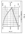
特定の実装例において、ハイブリッドレンズBの回折/屈折面(すなわちSurface ID 10)は図4に示される特徴を有し得る。これは、口径の中心からの半径/距離に応じてどのように相およびライン周波数が変化するかを示している。曲線102は相の変化を示し、曲線104はライン周波数の変化を示す。さらに、上記ハイブリッド回折/屈折面の回折次数は4に等しいが、その他の実装例において、回折次数は1または別の値に等しくてもよい。一般的に、回折次数は、製造し易さおよび/またはハイブリッド回折/屈折レンズBの直径に依存し得る。
In a particular implementation, the diffraction / refraction surface of hybrid lens B (ie, Surface ID 10) may have the features shown in FIG. This shows how the phase and line frequencies change depending on the radius / distance from the center of the aperture.
屈折率の値について、コンピュータモデリングは、屈折率データはシステム温度および圧力の大気に関連があり波長はシステム温度および圧力の大気中で測定されると想定した。波長0.940000μmに対し、絶対空気屈折率の値は、20℃で1.000270、60℃で1.000237、100℃で1.000212であった。 For index values, computer modeling assumed that index data was relevant to the system temperature and pressure atmosphere and wavelengths were measured in the system temperature and pressure atmosphere. For a wavelength of 0.940,000 μm, the value of the absolute air refractive index was 1.000270 at 20 ° C., 1.000237 at 60 ° C., and 1.000212 at 100 ° C.
上記詳細は例示に過ぎず、その他の実装例においてレンズおよびレンズ面のうちの1つ以上のさまざまな特性またはパラメータを調整することにより実質的にアサーマルな光学アセンブリを得ることができる。たとえば、上記実装例のいくつかのパラメータはさらに以下の表8のような有効焦点距離正規化パラメータで説明することができる。 The above details are merely exemplary, and substantially athermal optical assemblies can be obtained by adjusting one or more of the various properties or parameters of the lens and lens surface in other mounting examples. For example, some parameters of the above implementation example can be further explained by effective focal length normalization parameters as shown in Table 8 below.
上記実装例はさらにアスペクト比で説明することができる。この場合のアスペクト比は、最大直径光学面をハイブリッド光学アセンブリの総トラック長で除算したものであると定義される。たとえば、いくつかの実装例において、ハイブリッド光学アセンブリのアスペクト比は0.5であってもよく、その他の実装例において、このアスペクト比はハイブリッド光学アセンブリの意図される用途に応じてより大きくても小さくてもよい。たとえば、総トラック長が約4mmであるいくつかの実装例において、アスペクト比は約0.356であってもよく、総トラック長が約6.356であるその他いくつかの実装例において、アスペクト比は約0.224であってもよい。 The above implementation example can be further described in terms of aspect ratio. The aspect ratio in this case is defined as the maximum diameter optical plane divided by the total track length of the hybrid optical assembly. For example, in some implementations the aspect ratio of the hybrid optical assembly may be 0.5, and in other implementations this aspect ratio may be higher depending on the intended use of the hybrid optical assembly. It may be small. For example, in some implementations where the total track length is about 4 mm, the aspect ratio may be about 0.356, and in some other implementations where the total track length is about 6.356, the aspect ratio. May be about 0.224.
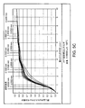
先に示したように、光学アセンブリ22は、投影面36にドットのアレイまたはその他のパターンを投影するように配置された光学パターン生成器の一部として統合されてもよい。コンピュータモデリングに基づく図5A、図5Bおよび図5Cのグラフに示されるように、光学アセンブリ22を用いて、ドットの高品質のアレイを投影面に投影することができる。図5A〜図5Cにおいて、各曲線(たとえば202、204)は異なるフィールドポイントを示し、これはたとえばVCSELアレイ22から投影されたドットである。グラフの上の値(すなわち0.000mm〜0.550mm)は、各フィールドポイントの、VCSELアレイ面の中心からの距離を示す。図5Aは20℃における曲線を示し、図5Bは60℃における曲線を示し、図5Cは100℃における曲線を示す。
As shown above, the
図5A〜図5Cにおける各曲線は、面36に投影されたドットの中心からの所与の半径を有する重心の中に閉じ込められた光エネルギの部分を示している。半径約3.5μmまでの曲線の傾斜の急峻さは、投影されたドットが高品質であることを示している(すなわち各ドットの光学エネルギのほとんどは半径約3.5μmの重心の中に含まれる)。さらに、投影されたドットのアレイの高い品質は実質的に20℃〜100℃の温度範囲にわたり維持される。すなわち、約20℃〜60℃の動作温度において、光の約80%が、可能なすべての光源(VCSEL)位置に対し、約3.4μmよりもわずかに小さい半径を有する円(ドット)に閉じ込められるのに対し、最大100℃までの動作温度では、光の約80%が、可能なすべての光源(VCSEL)位置に対し、約3.5μmよりもわずかに小さい半径を有する円に閉じ込められる。したがって、アサーマル光学アセンブリ20の出力の品質は、動作範囲20℃〜100℃にわたって実質的に一定である。このように、たとえ温度が変動しても高品質のシステム性能を得ることができる。
Each curve in FIGS. 5A-5C shows a portion of light energy confined within a center of gravity with a given radius from the center of the dots projected onto the
特徴のさまざまな修正および組合わせは上述の例から明白であり本発明の精神に含まれる。したがって、その他の実装例は請求項の範囲に含まれる。 Various modifications and combinations of features are evident from the examples above and are included in the spirit of the invention. Therefore, other implementation examples are included in the claims.
Claims (4)
発光素子のアレイと、
光学パターン投影のためのハイブリッド光学アセンブリとを備え、
前記ハイブリッド光学アセンブリは、
透明なホウケイ酸ガラスからなる第1の透過基板と、
前記第1の透過基板の第1の面上に配置されたエポキシからなる第1の非球面レンズと、
前記第1の透過基板の第1の面とは反対側の第2の面上に配置されたエポキシからなる第2のハイブリッド回折/屈折レンズと、
前記第1の透過基板から離隔した、透明なホウケイ酸ガラスからなる第2の透過基板と、
前記第2の透過基板の第1の面上に配置されたエポキシからなる第3の非球面レンズと、
前記第2の透過基板の第1の面とは反対側の第2の面上に配置されたエポキシからなる第4の非球面レンズとを含み、
前記第3の非球面レンズは、前記第2のハイブリッド回折/屈折レンズに面しており、
前記発光素子のアレイは、前記発光素子によって生成された光が、前記ハイブリッド光学アセンブリの前記第4の非球面レンズ、前記第3の非球面レンズ、前記第2のハイブリッド回折/屈折レンズ、および前記第1の非球面レンズをこの順で通過することにより、前記発光素子の配置に対応する光学ドットのパターンを投影するように、配置され、
前記発光素子はVCSELである、光学パターン生成器。 An optical pattern generator
An array of light emitting elements and
Equipped with a hybrid optical assembly for optical pattern projection,
The hybrid optical assembly
A first transparent substrate made of transparent borosilicate glass,
A first aspherical lens made of epoxy placed on the first surface of the first transmissive substrate, and
A second hybrid diffraction / refraction lens made of epoxy disposed on a second surface opposite to the first surface of the first transmissive substrate.
A second transparent substrate made of transparent borosilicate glass separated from the first transparent substrate, and a second transparent substrate.
A third aspherical lens made of epoxy placed on the first surface of the second transmissive substrate, and
A fourth aspherical lens made of epoxy disposed on a second surface opposite to the first surface of the second transmissive substrate.
The third aspherical lens faces the second hybrid diffraction / refraction lens.
In the array of light emitting elements, the light generated by the light emitting element is the fourth aspherical lens, the third aspherical lens, the second hybrid diffraction / refraction lens, and the light emitting element of the hybrid optical assembly. By passing through the first aspherical lens in this order, the light emitting element is arranged so as to project a pattern of optical dots corresponding to the arrangement of the light emitting element .
The light emitting device Ru VCSEL der, optical science pattern generator.
アレイまたはその他のパターンで配置された複数の光学素子から光を発するステップと、
前記発した光が、前記ハイブリッド光学アセンブリを通過するようにするステップと、
前記ハイブリッド光学アセンブリを通過した光を物体または平面上に投影するステップとを含み、前記投影した光はドットのパターンを形成する、方法。 A method of generating a pattern of optical dots using the optical pattern generator according to claim 1 or 2, wherein the method is:
Steps that emit light from multiple optics arranged in an array or other pattern,
A step to make the emitted light passes through the pre-Symbol hybrid optical assembly,
A method comprising the step of projecting light that has passed through the hybrid optical assembly onto an object or plane, wherein the projected light forms a pattern of dots.
Applications Claiming Priority (3)
| Application Number | Priority Date | Filing Date | Title |
|---|---|---|---|
| US201562245082P | 2015-10-22 | 2015-10-22 | |
| US62/245,082 | 2015-10-22 | ||
| PCT/SG2016/050512 WO2017069705A1 (en) | 2015-10-22 | 2016-10-21 | Athermal optical assembly |
Publications (4)
| Publication Number | Publication Date |
|---|---|
| JP2018531430A JP2018531430A (en) | 2018-10-25 |
| JP2018531430A6 JP2018531430A6 (en) | 2018-12-13 |
| JP2018531430A5 JP2018531430A5 (en) | 2019-06-27 |
| JP6952030B2 true JP6952030B2 (en) | 2021-10-20 |
Family
ID=58557499
Family Applications (1)
| Application Number | Title | Priority Date | Filing Date |
|---|---|---|---|
| JP2018520581A Active JP6952030B2 (en) | 2015-10-22 | 2016-10-21 | Athermal optical assembly |
Country Status (7)
| Country | Link |
|---|---|
| US (1) | US11073677B2 (en) |
| EP (1) | EP3365719B1 (en) |
| JP (1) | JP6952030B2 (en) |
| KR (1) | KR20180070669A (en) |
| CN (1) | CN108292026B (en) |
| TW (1) | TWI700517B (en) |
| WO (1) | WO2017069705A1 (en) |
Families Citing this family (3)
| Publication number | Priority date | Publication date | Assignee | Title |
|---|---|---|---|---|
| CN108107548B (en) * | 2017-11-03 | 2021-11-30 | 玉晶光电(厦门)有限公司 | Optical lens group |
| CN110471192B (en) * | 2018-05-11 | 2021-09-21 | 宁波舜宇光电信息有限公司 | Projection device, diffractive optical element, method for manufacturing the same, and electronic apparatus with projection device |
| US11067877B2 (en) | 2018-11-09 | 2021-07-20 | Samsung Electronics Co., Ltd. | Structured light projector and electronic device including the same |
Family Cites Families (24)
| Publication number | Priority date | Publication date | Assignee | Title |
|---|---|---|---|---|
| GB9013011D0 (en) * | 1990-06-11 | 1990-10-17 | Bae Plc | Hybrid petzval objective |
| US20030043463A1 (en) | 1992-03-30 | 2003-03-06 | Yajun Li | Athermalized plastic lens |
| JPH0943508A (en) * | 1995-07-28 | 1997-02-14 | Topcon Corp | Hybrid lens |
| US5745289A (en) | 1996-06-21 | 1998-04-28 | Eastman Kodak Company | Athermalized diffractive optical elements |
| US5963375A (en) * | 1996-01-31 | 1999-10-05 | U.S. Precision Lens Inc. | Athermal LCD projection lens |
| DE69726352T2 (en) * | 1996-08-16 | 2004-09-09 | 3M Innovative Properties Co., St. Paul | Miniature projection zoom lens for use with pixel matrix display board |
| JP3720187B2 (en) * | 1998-02-23 | 2005-11-24 | 株式会社リコー | lens |
| JP3686253B2 (en) | 1998-04-10 | 2005-08-24 | オリンパス株式会社 | Zoom lens using diffractive optical element |
| WO2000013048A1 (en) | 1998-08-28 | 2000-03-09 | Ksm Associates, Inc. | Optical systems employing stepped diffractive surfaces |
| EP1075150A3 (en) * | 1999-07-31 | 2005-04-27 | Lg Electronics Inc. | Projection lens system |
| JP3634736B2 (en) | 2000-10-12 | 2005-03-30 | ペンタックス株式会社 | Objective lens for optical head and optical system of optical head |
| JP2002350973A (en) | 2001-05-23 | 2002-12-04 | Kanto Auto Works Ltd | Projector |
| CN1213323C (en) | 2002-04-29 | 2005-08-03 | 南开大学 | Infrared refraction-diffraction three-piece heat-abstraction optical imaging system structure |
| JP2004126393A (en) | 2002-10-04 | 2004-04-22 | Nikon Corp | Imaging lens and transmitter-receiver using the same |
| KR20040061658A (en) | 2002-12-31 | 2004-07-07 | 삼성전자주식회사 | Hybrid achromatic optical lens and manufacturing method thereof |
| KR100665176B1 (en) * | 2005-05-18 | 2007-01-09 | 삼성전기주식회사 | Wafer Scale Lens and Optical System Having The Same |
| JP2008077728A (en) | 2006-09-20 | 2008-04-03 | Canon Inc | Objective lens and optical pickup device using the same |
| WO2008102773A1 (en) * | 2007-02-19 | 2008-08-28 | Konica Minolta Opto, Inc. | Imaging lens, imaging device, portable terminal and method for manufacturing imaging lens |
| WO2008110264A1 (en) | 2007-03-15 | 2008-09-18 | Swiss Medical Technology Gmbh | Magnification loupe with aspherical lenses |
| EP2223173B1 (en) | 2007-12-19 | 2013-09-04 | Heptagon Micro Optics Pte. Ltd. | Camera device and manufacturing methods therefor |
| US20120206641A1 (en) | 2009-10-06 | 2012-08-16 | Sony Corporation | Optical unit and image pickup apparatus |
| CN102472839B (en) | 2010-04-27 | 2015-05-13 | 柯尼卡美能达精密光学株式会社 | Image capture lens, wafer lens, wafer lens laminate, method of manufacturing image capture lens, image capture lens intermediate product, method of manufacturing image capture lens intermediate product |
| JP2012103461A (en) * | 2010-11-10 | 2012-05-31 | Topcon Corp | Infrared optical system |
| US9094593B2 (en) | 2013-07-30 | 2015-07-28 | Heptagon Micro Optics Pte. Ltd. | Optoelectronic modules that have shielding to reduce light leakage or stray light, and fabrication methods for such modules |
-
2016
- 2016-10-21 JP JP2018520581A patent/JP6952030B2/en active Active
- 2016-10-21 KR KR1020187014074A patent/KR20180070669A/en not_active Application Discontinuation
- 2016-10-21 US US15/769,916 patent/US11073677B2/en active Active
- 2016-10-21 TW TW105134196A patent/TWI700517B/en active
- 2016-10-21 CN CN201680068032.2A patent/CN108292026B/en active Active
- 2016-10-21 EP EP16857899.5A patent/EP3365719B1/en active Active
- 2016-10-21 WO PCT/SG2016/050512 patent/WO2017069705A1/en active Application Filing
Also Published As
| Publication number | Publication date |
|---|---|
| EP3365719B1 (en) | 2022-11-30 |
| US11073677B2 (en) | 2021-07-27 |
| TW201732322A (en) | 2017-09-16 |
| CN108292026A (en) | 2018-07-17 |
| JP2018531430A (en) | 2018-10-25 |
| TWI700517B (en) | 2020-08-01 |
| CN108292026B (en) | 2021-11-26 |
| WO2017069705A1 (en) | 2017-04-27 |
| EP3365719A1 (en) | 2018-08-29 |
| EP3365719A4 (en) | 2019-06-26 |
| KR20180070669A (en) | 2018-06-26 |
| US20200064584A1 (en) | 2020-02-27 |
Similar Documents
| Publication | Publication Date | Title |
|---|---|---|
| CN107505689B (en) | Projection lens system | |
| JP6664621B2 (en) | Method of manufacturing optical system including microlens array | |
| CN109557650B (en) | Collimating lens and projection module | |
| JP6952030B2 (en) | Athermal optical assembly | |
| CN108227149B (en) | Collimation lens | |
| CN108318996B (en) | Collimation lens | |
| CN107436484B (en) | Projection lens | |
| TWI778765B (en) | Illumination device | |
| JP2021507279A (en) | Optical system | |
| US20200133012A1 (en) | Optical element and optical system | |
| JP2018531430A6 (en) | Athermal optical assembly | |
| CN208092311U (en) | Collimate camera lens | |
| JP7253612B2 (en) | Apparatus for collimating a ray field | |
| JP2018531430A5 (en) | ||
| US20190302596A1 (en) | Optical module | |
| TWI708961B (en) | Illumination assembly for 3d data acquisition | |
| US20240019703A1 (en) | Shock absorbers in an optical assembly for a wearable display device | |
| WO2022018891A1 (en) | Light source device | |
| JP5425893B2 (en) | Collimating lens | |
| TWI589932B (en) | Collimating lens | |
| EP4078275A1 (en) | Virtual image display optical architectures | |
| JPWO2019116469A1 (en) | Optical element and parallel light generator | |
| Schimmel et al. | Designing beam shaping systems basing on spherical catalog lenses | |
| TWM495524U (en) | Apparatus of generating structured lighting | |
| KR20120106437A (en) | Lens that has a cross section including an extended conic curve and its design method |
Legal Events
| Date | Code | Title | Description |
|---|---|---|---|
| A521 | Request for written amendment filed |
Free format text: JAPANESE INTERMEDIATE CODE: A523 Effective date: 20190522 |
|
| A621 | Written request for application examination |
Free format text: JAPANESE INTERMEDIATE CODE: A621 Effective date: 20190522 |
|
| A131 | Notification of reasons for refusal |
Free format text: JAPANESE INTERMEDIATE CODE: A131 Effective date: 20200204 |
|
| A521 | Request for written amendment filed |
Free format text: JAPANESE INTERMEDIATE CODE: A523 Effective date: 20200428 |
|
| A131 | Notification of reasons for refusal |
Free format text: JAPANESE INTERMEDIATE CODE: A131 Effective date: 20200929 |
|
| A601 | Written request for extension of time |
Free format text: JAPANESE INTERMEDIATE CODE: A601 Effective date: 20201009 |
|
| A601 | Written request for extension of time |
Free format text: JAPANESE INTERMEDIATE CODE: A601 Effective date: 20210226 |
|
| A521 | Request for written amendment filed |
Free format text: JAPANESE INTERMEDIATE CODE: A523 Effective date: 20210326 |
|
| TRDD | Decision of grant or rejection written | ||
| A01 | Written decision to grant a patent or to grant a registration (utility model) |
Free format text: JAPANESE INTERMEDIATE CODE: A01 Effective date: 20210831 |
|
| A61 | First payment of annual fees (during grant procedure) |
Free format text: JAPANESE INTERMEDIATE CODE: A61 Effective date: 20210927 |
|
| R150 | Certificate of patent or registration of utility model |
Ref document number: 6952030 Country of ref document: JP Free format text: JAPANESE INTERMEDIATE CODE: R150 |