EP3365719B1 - Athermal optical assembly - Google Patents
Athermal optical assembly Download PDFInfo
- Publication number
- EP3365719B1 EP3365719B1 EP16857899.5A EP16857899A EP3365719B1 EP 3365719 B1 EP3365719 B1 EP 3365719B1 EP 16857899 A EP16857899 A EP 16857899A EP 3365719 B1 EP3365719 B1 EP 3365719B1
- Authority
- EP
- European Patent Office
- Prior art keywords
- order
- lens
- aspheric
- hybrid
- diffractive
- Prior art date
- Legal status (The legal status is an assumption and is not a legal conclusion. Google has not performed a legal analysis and makes no representation as to the accuracy of the status listed.)
- Active
Links
- 230000003287 optical effect Effects 0.000 title claims description 82
- 239000000758 substrate Substances 0.000 claims description 10
- 239000005388 borosilicate glass Substances 0.000 claims description 7
- 238000000034 method Methods 0.000 claims description 4
- 239000004593 Epoxy Substances 0.000 claims 4
- 230000000712 assembly Effects 0.000 description 9
- 238000000429 assembly Methods 0.000 description 9
- 239000000463 material Substances 0.000 description 5
- 238000005094 computer simulation Methods 0.000 description 4
- 230000008859 change Effects 0.000 description 3
- 238000005286 illumination Methods 0.000 description 3
- 238000013507 mapping Methods 0.000 description 3
- 239000011521 glass Substances 0.000 description 2
- 230000005855 radiation Effects 0.000 description 2
- 230000002411 adverse Effects 0.000 description 1
- 230000004075 alteration Effects 0.000 description 1
- 238000012937 correction Methods 0.000 description 1
- 230000001419 dependent effect Effects 0.000 description 1
- 238000013461 design Methods 0.000 description 1
- 239000006185 dispersion Substances 0.000 description 1
- 238000006073 displacement reaction Methods 0.000 description 1
- 239000003822 epoxy resin Substances 0.000 description 1
- 238000003384 imaging method Methods 0.000 description 1
- 238000004519 manufacturing process Methods 0.000 description 1
- 238000012986 modification Methods 0.000 description 1
- 230000004048 modification Effects 0.000 description 1
- 230000005693 optoelectronics Effects 0.000 description 1
- 229920000647 polyepoxide Polymers 0.000 description 1
- 230000008569 process Effects 0.000 description 1
- 239000000126 substance Substances 0.000 description 1
Images


Classifications
-
- G—PHYSICS
- G02—OPTICS
- G02B—OPTICAL ELEMENTS, SYSTEMS OR APPARATUS
- G02B7/00—Mountings, adjusting means, or light-tight connections, for optical elements
- G02B7/02—Mountings, adjusting means, or light-tight connections, for optical elements for lenses
- G02B7/028—Mountings, adjusting means, or light-tight connections, for optical elements for lenses with means for compensating for changes in temperature or for controlling the temperature; thermal stabilisation
-
- G—PHYSICS
- G02—OPTICS
- G02B—OPTICAL ELEMENTS, SYSTEMS OR APPARATUS
- G02B7/00—Mountings, adjusting means, or light-tight connections, for optical elements
- G02B7/008—Mountings, adjusting means, or light-tight connections, for optical elements with means for compensating for changes in temperature or for controlling the temperature; thermal stabilisation
-
- G—PHYSICS
- G02—OPTICS
- G02B—OPTICAL ELEMENTS, SYSTEMS OR APPARATUS
- G02B13/00—Optical objectives specially designed for the purposes specified below
- G02B13/18—Optical objectives specially designed for the purposes specified below with lenses having one or more non-spherical faces, e.g. for reducing geometrical aberration
-
- G—PHYSICS
- G02—OPTICS
- G02B—OPTICAL ELEMENTS, SYSTEMS OR APPARATUS
- G02B27/00—Optical systems or apparatus not provided for by any of the groups G02B1/00 - G02B26/00, G02B30/00
- G02B27/0025—Optical systems or apparatus not provided for by any of the groups G02B1/00 - G02B26/00, G02B30/00 for optical correction, e.g. distorsion, aberration
- G02B27/0037—Optical systems or apparatus not provided for by any of the groups G02B1/00 - G02B26/00, G02B30/00 for optical correction, e.g. distorsion, aberration with diffracting elements
-
- G—PHYSICS
- G02—OPTICS
- G02B—OPTICAL ELEMENTS, SYSTEMS OR APPARATUS
- G02B27/00—Optical systems or apparatus not provided for by any of the groups G02B1/00 - G02B26/00, G02B30/00
- G02B27/0025—Optical systems or apparatus not provided for by any of the groups G02B1/00 - G02B26/00, G02B30/00 for optical correction, e.g. distorsion, aberration
- G02B27/005—Optical systems or apparatus not provided for by any of the groups G02B1/00 - G02B26/00, G02B30/00 for optical correction, e.g. distorsion, aberration for correction of secondary colour or higher-order chromatic aberrations
- G02B27/0056—Optical systems or apparatus not provided for by any of the groups G02B1/00 - G02B26/00, G02B30/00 for optical correction, e.g. distorsion, aberration for correction of secondary colour or higher-order chromatic aberrations by using a diffractive optical element
-
- G—PHYSICS
- G02—OPTICS
- G02B—OPTICAL ELEMENTS, SYSTEMS OR APPARATUS
- G02B27/00—Optical systems or apparatus not provided for by any of the groups G02B1/00 - G02B26/00, G02B30/00
- G02B27/42—Diffraction optics, i.e. systems including a diffractive element being designed for providing a diffractive effect
- G02B27/4205—Diffraction optics, i.e. systems including a diffractive element being designed for providing a diffractive effect having a diffractive optical element [DOE] contributing to image formation, e.g. whereby modulation transfer function MTF or optical aberrations are relevant
- G02B27/4211—Diffraction optics, i.e. systems including a diffractive element being designed for providing a diffractive effect having a diffractive optical element [DOE] contributing to image formation, e.g. whereby modulation transfer function MTF or optical aberrations are relevant correcting chromatic aberrations
-
- G—PHYSICS
- G02—OPTICS
- G02B—OPTICAL ELEMENTS, SYSTEMS OR APPARATUS
- G02B27/00—Optical systems or apparatus not provided for by any of the groups G02B1/00 - G02B26/00, G02B30/00
- G02B27/42—Diffraction optics, i.e. systems including a diffractive element being designed for providing a diffractive effect
- G02B27/4233—Diffraction optics, i.e. systems including a diffractive element being designed for providing a diffractive effect having a diffractive element [DOE] contributing to a non-imaging application
-
- G—PHYSICS
- G02—OPTICS
- G02B—OPTICAL ELEMENTS, SYSTEMS OR APPARATUS
- G02B5/00—Optical elements other than lenses
- G02B5/18—Diffraction gratings
- G02B5/1876—Diffractive Fresnel lenses; Zone plates; Kinoforms
Definitions
- This disclosure relates to optical assemblies.
- Optical assemblies are used in a wide range of commercial, industrial and military devices and systems.
- the assemblies may include, for example, various types of passive optical elements such as diffractive, refractive or reflective components.
- hybrid optical elements can be advantageous.
- a hybrid optical element can have a diffractive surface that is etched, micro-machined or embossed, for example, onto the surface of a refractive or reflective optical component.
- Such hybrid elements can, in some cases, provide enhanced flexibility in the selection of materials based, for example, on dispersion and thermal behavior of the refractive materials.
- an optical assembly may be integrated into an optoelectronic module that also includes a light emitting element such as a vertical cavity surface-emitting laser (VCSEL) operable to emit infra-red (IR) radiation.
- VCSEL vertical cavity surface-emitting laser
- IR infra-red
- Operation of the VCSEL in close proximity to the optical assembly may result in thermally-induced changes to the optical elements of the assembly.
- the optical assembly includes polymeric lenses
- changes in temperature may result in changes to the dimensions and/or the refractive index of the lenses. Such changes can, in turn, cause the output of the optical assembly to deviate from the optimal specifications.
- an athermal optical assembly i.e., an optical assembly that generates output with substantial stability over a wide variation in temperature.
- optical assemblies in other words, optical assemblies that generate output with substantial stability over a wide variation in temperature.
- the optical assemblies can be integrated, for example, as part of array generators arranged to project an array or other pattern of dots onto an object or projection plane.
- optical pattern generator according to the invention is defined in appended independent claim 1.
- a method of generating a pattern of optical dots is defined in appended independent claim 3.
- the present disclosure describes hybrid athermal optical assemblies that can be integrated, for example, into array generators arranged to project an array or other pattern of dots.
- Optical pattern projection can be used in a variety of applications such as three-dimensional (3D) or depth mapping, area illumination, and LCD backlighting.
- 3D (or depth) mapping refers to a set of 3D coordinates representing the surface of an object.
- light i.e., visible, infra-red, or other radiation
- a region with a pattern of high quality e.g., good resolution, and with dots of optimal encircled energy
- well-controlled intensity e.g., from 20°C to 100°C.
- a hybrid optical assembly 20 includes several passive optical elements, i.e., lenses A, B, C and D. Two of the lenses, A and B, are disposed on opposite sides of a first transmissive (e.g., glass or wafer) substrate 32; the other two lenses, C and D, are disposed on opposite sides of a second transmissive (e.g., glass or wafer) substrate 34.
- the optical axes of the lenses A, B, C and D are aligned with one another, and the inner surfaces of the lenses B and C are separated from one another by a distance d, which for some applications is in the range of several (e.g., four) millimeters (mm) to about ten mm.
- the optical axes may be aligned, the geometric path may not be aligned; for example, in implementations having a folded optical path, the geometric path is not aligned, whereas the optical axes of the lenses A, B, C and D are aligned.
- An array 22 of light emitting elements such as a VCSELs, can be placed in front of the optical assembly 20 such that lens D is closest to the VCSEL array 22 and the lens A is furthest from the VCSEL array 22.
- Such an implementation can be particularly advantageous is some cases because the overall footprint of the assembly can be reduced (i.e., by increasing its thickness - the dimension orthogonal to the footprint).
- the optical assembly 20 is arranged such that when light (e.g., IR light) from the VCSEL array 22 is emitted toward the optical assembly 20, an array of well-defined optical dots 38 appears on the projection plane 36.
- the various lenses A, B, C and D help collimate and focus the light, such that the array of dots 38 appearing on the projection plane 26 corresponds, for example, to the arrangement of the VCSELs in the array 22.
- FIG. 2 illustrates a particular arrangement of the VCSEL array 22; other arrangements, and other numbers of VCSEL emitters within the array 22, can be provided for other implementations.
- lenses A, C and D are implemented as aspherical lenses.
- aspheric lenses can be designed, for example, with surfaces of the form: where the optic axis is presumed to lie in the z-direction, and z(r) is the sag, i.e., the z-component of the displacement of the surface from the vertex, at distance r from the axis.
- the aspheric coefficients ⁇ i describe the deviation of the surface from the axially symmetric quadric surface specified by R and ⁇ . See FIG. 3 .
- lens B is implemented as a hybrid diffractive/refractive lens.
- Lens B can be described using the aspheric equation above in combination with the following polynomial expansion describing the diffractive phase ⁇ of lens B: where M is the diffraction order of the hybrid diffractive/refractive lens, N is the number of polynomial coefficients in the series, A i is the coefficient on the 2i th power of ⁇ , and ⁇ is the normalized radial aperture coordinate. Specific examples of the lens characteristics and their respective properties for particular implementations are described below.
- lenses A through D are such that the optical assembly 20 is substantially athermal (i.e., its output exhibits substantial stability over a wide variation in temperature, for example, over the range 20°C to 100°C). Further, lenses (e.g., lenses A through D) also can provide for aberration correction.
- the example hybrid optical assemblies described below can be modeled or simulated by, for example, sequential and/or non-sequential ray-tracing simulation software such as Zemax, the numerals included below describe the various components (e.g., thicknesses, diameters, surface shapes, coefficients) and their position within the illumination assembly, these numerals include a plurality of decimal places.
- the aspheric coefficients used to describe the aspheric surfaces of various components below can include as many as nine decimals places or more.
- up to nine decimals places are included, in some cases far fewer decimal places are needed to adequately describe the various components and their respective position within the illumination assembly.
- no more than two or three or four decimal places are required in order to effectively describe various components and their respective position within the hybrid optical assembly further described below.
- optical assembly 20 Multiple surfaces define the optical assembly 20, including the lenses A through D.
- Table I describes the various surfaces in the optical assembly 20 and the VCSEL array 22 for some implementations with a total track length of about 4 mm.
- lens A is defined by surfaces 4 and 6; lens B is defined by surfaces 8, 9 and 10; lens C is defined by surfaces 13 and 14; and lens D is defined by surfaces 16, 17 and 18.
- Table II describes the various surface shapes, coefficients, and characteristics of the optical surfaces within the optical assembly 20 and the VCSEL array 22 for some implementations with a total track length of about 4 mm. In this implementation, the conic for each of the surfaces is zero. Further, although this implementation is described by an aspheric polynomial and a polynomial expansion describing the diffractive phase of lens B, other ways of describing the surfaces are within the scope of this disclosure.
- Table III below, describes further information pertaining to the foregoing implementation.
- Table IV describes the various surfaces in the optical assembly 20 and the VCSEL array 22 for some implementations with a total track length of about 6.356 mm.
- lens A is defined by surfaces 4 and 6; lens B is defined by surfaces 8, 9 and 10; lens C is defined by surfaces 13 and 14; and lens D is defined by surfaces 16, 17 and 18.
- Table V describes the various surface shapes and characteristics of the optical surfaces within the optical assembly 20 and the VCSEL array 22 for some implementations with a total track length of about 6.356 mm. In this implementation, the conic for each of the surfaces is zero. Further, although this implementation is described by an aspheric polynomial and a polynomial expansion describing the diffractive phase of lens B, other ways of describing the surfaces are within the scope of this disclosure.
- Table VI below, describes further information pertaining to the implementation described above.
- D263TECO is a clear borosilicate glass of high chemical resistance
- R14 is an epoxy resin. Further properties of these materials are set forth in Table VII below. Other lens materials may be used for some implementations.
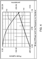
- the diffractive/refractive surface (i.e., Surface ID 10) of the hybrid lens B is can have characteristics as shown in FIG. 4 , which indicates how phase and line frequency change with radius/distance from the center of the aperture.
- the curve 102 indicates the change in phase
- the curve 104 indicates the change in line frequency.
- the diffraction order of the hybrid diffractive/refractive surfaces described above is equal to four, in other implementations the diffraction order can be equal to one or another value. In general, the diffraction order may depend on the ease of manufacturing and/or the diameter of the hybrid diffractive/refractive lens B.
- the computer modeling assumed that the index data is relative to air at the system temperature and pressure and that wavelengths are measured in air at the system temperature and pressure.
- the absolute air index values were 1.000270 at 20°C, 1.000237 at 60°C, and 1.000212 at 100°C.
- the described implementations can be additionally described in terms of an aspect ratio where the aspect ratio is defined as the largest diameter optical surface divided by the total track length of the hybrid optical assembly.
- the aspect ratio of the hybrid optical assembly can be 0.5, while in other implementations that aspect ratio can be larger or smaller depending on the intended application of the hybrid optical assembly.
- the aspect ratio can be about 0.356, while for some other implementations with a total track length of about 6.356 the aspect ratio can be about 0.224.
- the optical assembly 22 can be integrated as part of an optical pattern generator arranged to project an array or other pattern of dots onto a projection plane 36. As illustrated in the graphs of FIGS. 5A , 5B and 5C based on computer modeling, the optical assembly 22 can be used to project a high-quality array of dots onto the projection plane.
- each curve e.g., 202, 204 represents a different field point, for example, a projected dot from the VCSEL array 22.
- the values above the top of the graph i.e., 0.000mm - 0.550 mm
- FIG. 5A illustrates the curves at 20°C
- FIG. 5B illustrates the curves at 60°C
- FIG. 5C illustrates the curves at 100°C.
- Each curve in FIGS. 5A - 5C indicates the fraction of the optical energy enclosed within a centroid having a given radius from the center of the dot projected onto the plane 36.
- the steepness of the slopes of the curves out to a radius of about 3.5 ⁇ m is indicative of the high quality of the projected dots (i.e., most of the optical energy for each dot is contained within a centroid having a radius of about 3.5 ⁇ m). Further, the high quality of the projected array of dots substantially is maintained over the temperature range of 20°C - 100°C.
- the quality of the output of the athermal optical assembly 20 is substantially constant over the operating range 20°C to 100°C.
- high quality system performance can be achieved even as the temperature varies.
Landscapes
- Physics & Mathematics (AREA)
- General Physics & Mathematics (AREA)
- Optics & Photonics (AREA)
- Lenses (AREA)
- Diffracting Gratings Or Hologram Optical Elements (AREA)
- Semiconductor Lasers (AREA)
Description
- This disclosure relates to optical assemblies.
- Optical assemblies are used in a wide range of commercial, industrial and military devices and systems. The assemblies may include, for example, various types of passive optical elements such as diffractive, refractive or reflective components. For some applications, hybrid optical elements can be advantageous. A hybrid optical element can have a diffractive surface that is etched, micro-machined or embossed, for example, onto the surface of a refractive or reflective optical component. Such hybrid elements can, in some cases, provide enhanced flexibility in the selection of materials based, for example, on dispersion and thermal behavior of the refractive materials.
- Depending on the application, various factors such as temperature variations may adversely impact the performance of the optical assembly. For example, in some situations, an optical assembly may be integrated into an optoelectronic module that also includes a light emitting element such as a vertical cavity surface-emitting laser (VCSEL) operable to emit infra-red (IR) radiation. Operation of the VCSEL in close proximity to the optical assembly may result in thermally-induced changes to the optical elements of the assembly. For example, if the optical assembly includes polymeric lenses, changes in temperature may result in changes to the dimensions and/or the refractive index of the lenses. Such changes can, in turn, cause the output of the optical assembly to deviate from the optimal specifications.
- In view of the foregoing or other problems, it is desirable in some applications to provide an athermal optical assembly (i.e., an optical assembly that generates output with substantial stability over a wide variation in temperature).
Further background information can be found in the following documents: -
CN1455282 describes an optical design imaging system for the mid infrared band which uses a refractive diffractive hybrid lens for temperature stability. -
US2002089763 describes a single objective lens for an optical disc drive having a periphery provided with a diffractive lens structure. - The invention is set out in the independent claims.
- This disclosure describes athermal optical assemblies, in other words, optical assemblies that generate output with substantial stability over a wide variation in temperature. The optical assemblies can be integrated, for example, as part of array generators arranged to project an array or other pattern of dots onto an object or projection plane.
- An optical pattern generator according to the invention is defined in appended
independent claim 1. - In accordance with another aspect of the invention, a method of generating a pattern of optical dots is defined in appended
independent claim 3. - Further embodiments are defined in the dependent claims.
- Other aspects, features and advantages will be readily apparent from the following detailed description, the accompanying drawings, and the claims.
-
-
FIG. 1 illustrates an example of an optical array generator that includes an athermal optical assembly. -
FIG. 2 illustrates an example of an array of optical dots projected onto a projection plane by the optical array generator ofFIG. 1 . -
FIG. 3 illustrates an example of an aspheric lens. -
FIG. 4 illustrates properties of an example of a hybrid diffractive/refractive lens that can be included in the optical assembly. -
FIGS. 5A ,5B and5C are graphs illustrating performance of the optical assembly at different temperatures. - The present disclosure describes hybrid athermal optical assemblies that can be integrated, for example, into array generators arranged to project an array or other pattern of dots. Optical pattern projection can be used in a variety of applications such as three-dimensional (3D) or depth mapping, area illumination, and LCD backlighting. 3D (or depth) mapping, for example, refers to a set of 3D coordinates representing the surface of an object. As part of the process of depth mapping, light (i.e., visible, infra-red, or other radiation) can be projected onto a region with a pattern of high quality (e.g., good resolution, and with dots of optimal encircled energy) and well-controlled intensity, so that depth values can be found reliably over a substantial part of an object or objects in a scene and over a range of operating temperatures (e.g., from 20°C to 100°C).
- As shown in
FIG. 1 , a hybridoptical assembly 20 includes several passive optical elements, i.e., lenses A, B, C and D. Two of the lenses, A and B, are disposed on opposite sides of a first transmissive (e.g., glass or wafer)substrate 32; the other two lenses, C and D, are disposed on opposite sides of a second transmissive (e.g., glass or wafer)substrate 34. The optical axes of the lenses A, B, C and D are aligned with one another, and the inner surfaces of the lenses B and C are separated from one another by a distance d, which for some applications is in the range of several (e.g., four) millimeters (mm) to about ten mm. In some implementations, although the optical axes may be aligned, the geometric path may not be aligned; for example, in implementations having a folded optical path, the geometric path is not aligned, whereas the optical axes of the lenses A, B, C and D are aligned. Anarray 22 of light emitting elements, such as a VCSELs, can be placed in front of theoptical assembly 20 such that lens D is closest to theVCSEL array 22 and the lens A is furthest from theVCSEL array 22. Such an implementation can be particularly advantageous is some cases because the overall footprint of the assembly can be reduced (i.e., by increasing its thickness - the dimension orthogonal to the footprint). - As illustrated in
FIG. 2 , theoptical assembly 20 is arranged such that when light (e.g., IR light) from theVCSEL array 22 is emitted toward theoptical assembly 20, an array of well-definedoptical dots 38 appears on theprojection plane 36. Collectively, the various lenses A, B, C and D help collimate and focus the light, such that the array ofdots 38 appearing on the projection plane 26 corresponds, for example, to the arrangement of the VCSELs in thearray 22.FIG. 2 illustrates a particular arrangement of the VCSELarray 22; other arrangements, and other numbers of VCSEL emitters within thearray 22, can be provided for other implementations. - In the illustrated example, lenses A, C and D are implemented as aspherical lenses. In general, aspheric lenses can be designed, for example, with surfaces of the form:

FIG. 3 . On the other hand, lens B is implemented as a hybrid diffractive/refractive lens. Lens B can be described using the aspheric equation above in combination with the following polynomial expansion describing the diffractive phase Φ of lens B:
- The specific properties of the lenses A through D are such that the
optical assembly 20 is substantially athermal (i.e., its output exhibits substantial stability over a wide variation in temperature, for example, over therange 20°C to 100°C). Further, lenses (e.g., lenses A through D) also can provide for aberration correction. - Computer modeling was used to determine how different properties of the lenses and the optical assembly would vary with changes in temperature. Data describing implementations of hybrid optical assemblies are indicated in Tables I - VI, below. The dimensions (radius, thickness and diameter) associated with each surface based on the computer modeling is set forth in Table I and VI (in microns (µm)). Further surface coefficients describing the shapes of lens surfaces and the characteristics of the hybrid refractive/diffractive element B are described in Tables II and V. Different dimensions may be appropriate for other implementations, however. Further the example hybrid optical assemblies described below can be modeled or simulated by, for example, sequential and/or non-sequential ray-tracing simulation software such as Zemax, the numerals included below describe the various components (e.g., thicknesses, diameters, surface shapes, coefficients) and their position within the illumination assembly, these numerals include a plurality of decimal places. For example the aspheric coefficients used to describe the aspheric surfaces of various components below can include as many as nine decimals places or more. However, although up to nine decimals places are included, in some cases far fewer decimal places are needed to adequately describe the various components and their respective position within the illumination assembly. For example, in some cases no more than two or three or four decimal places are required in order to effectively describe various components and their respective position within the hybrid optical assembly further described below.
- Multiple surfaces define the
optical assembly 20, including the lenses A through D. Table I, below, describes the various surfaces in theoptical assembly 20 and theVCSEL array 22 for some implementations with a total track length of about 4 mm.
- Thus, lens A is defined by
surfaces surfaces optical assembly 20 and theVCSEL array 22 for some implementations with a total track length of about 4 mm. In this implementation, the conic for each of the surfaces is zero. Further, although this implementation is described by an aspheric polynomial and a polynomial expansion describing the diffractive phase of lens B, other ways of describing the surfaces are within the scope of this disclosure.


- Table III, below, describes further information pertaining to the foregoing implementation.

- The foregoing information (i.e., in Tables I, II and III) is non-limiting and is provided as examples to enable a person of ordinary skill to make and use the invention.
- Table IV, below, describes the various surfaces in the
optical assembly 20 and theVCSEL array 22 for some implementations with a total track length of about 6.356 mm.
- Thus, lens A is defined by
surfaces surfaces optical assembly 20 and theVCSEL array 22 for some implementations with a total track length of about 6.356 mm. In this implementation, the conic for each of the surfaces is zero. Further, although this implementation is described by an aspheric polynomial and a polynomial expansion describing the diffractive phase of lens B, other ways of describing the surfaces are within the scope of this disclosure.


- Table VI, below, describes further information pertaining to the implementation described above.

- The foregoing information (i.e., in Tables IV, V and VI) is non-limiting and is provided as examples to enable a person of ordinary skill to make and use the invention
- Among the listed lens materials, D263TECO is a clear borosilicate glass of high chemical resistance, and R14 is an epoxy resin. Further properties of these materials are set forth in Table VII below. Other lens materials may be used for some implementations.

- For a particular implementation, the diffractive/refractive surface (i.e., Surface ID 10) of the hybrid lens B is can have characteristics as shown in
FIG. 4 , which indicates how phase and line frequency change with radius/distance from the center of the aperture. Thecurve 102 indicates the change in phase, whereas thecurve 104 indicates the change in line frequency. Further, although the diffraction order of the hybrid diffractive/refractive surfaces described above is equal to four, in other implementations the diffraction order can be equal to one or another value. In general, the diffraction order may depend on the ease of manufacturing and/or the diameter of the hybrid diffractive/refractive lens B. - For the values of index of refraction, the computer modeling assumed that the index data is relative to air at the system temperature and pressure and that wavelengths are measured in air at the system temperature and pressure. For a wavelength of 0.940000 µm, the absolute air index values were 1.000270 at 20°C, 1.000237 at 60°C, and 1.000212 at 100°C.
- The foregoing details are illustrative only, and various properties or parameters of one or more of the lenses and lens surfaces can be adjusted in other implementations so as to obtain a substantially athermal optical assembly. For example, some parameters of the described implementations can be additionally described in terms of effective-focal-length normalized parameters such as in Table 8 below:

- The described implementations can be additionally described in terms of an aspect ratio where the aspect ratio is defined as the largest diameter optical surface divided by the total track length of the hybrid optical assembly. For example, in some implementations the aspect ratio of the hybrid optical assembly can be 0.5, while in other implementations that aspect ratio can be larger or smaller depending on the intended application of the hybrid optical assembly. For example, for some implementations with a total track length about 4 mm, the aspect ratio can be about 0.356, while for some other implementations with a total track length of about 6.356 the aspect ratio can be about 0.224.
- As indicated previously, the
optical assembly 22 can be integrated as part of an optical pattern generator arranged to project an array or other pattern of dots onto aprojection plane 36. As illustrated in the graphs ofFIGS. 5A ,5B and5C based on computer modeling, theoptical assembly 22 can be used to project a high-quality array of dots onto the projection plane. InFIGS. 5A - 5C , each curve (e.g., 202, 204) represents a different field point, for example, a projected dot from theVCSEL array 22. The values above the top of the graph (i.e., 0.000mm - 0.550 mm) indicate the distance of each field point from the center of the VCSEL array plane.FIG. 5A illustrates the curves at 20°C,FIG. 5B illustrates the curves at 60°C, andFIG. 5C illustrates the curves at 100°C. - Each curve in
FIGS. 5A - 5C indicates the fraction of the optical energy enclosed within a centroid having a given radius from the center of the dot projected onto theplane 36. The steepness of the slopes of the curves out to a radius of about 3.5 µm is indicative of the high quality of the projected dots (i.e., most of the optical energy for each dot is contained within a centroid having a radius of about 3.5 µm). Further, the high quality of the projected array of dots substantially is maintained over the temperature range of 20°C - 100°C. That is, at an operating temperature of about 20°C - 60°C, about 80% of light is enclosed in a circle (a dot) with a radius slightly less than about 3.4 µm for all possible light source (VCSEL) positions, whereas up to an operating temperature of about 100°C, about 80% of light is enclosed in a circle with a radius slightly less than about 3.5 µm for all possible light source (VCSEL) positions. Accordingly, the quality of the output of the athermaloptical assembly 20 is substantially constant over theoperating range 20°C to 100°C. Thus, high quality system performance can be achieved even as the temperature varies. - Various modifications and combinations of features will be evident from the foregoing examples. Accordingly, other implementations are within the scope of the claims.
Claims (10)
- An optical pattern generator characterized by comprising:an array of light emitting elements, wherein the light emitting elements are VCSELs (22); anda hybrid optical assembly (20) for optical pattern projection;wherein the hybrid optical assembly (20) comprises:a first transmissive substrate (32) composed of clear borosilicate glass;a first aspherical lens (A) composed of epoxy disposed on a first side of the first clear borosilicate glass transmissive substrate (32);a second hybrid diffractive/refractive lens (B) composed of epoxy disposed on a second, opposite side of the first clear borosilicate glass transmissive substrate (32);a second transmissive substrate (34) composed of clear borosilicate glass, separated from the first transmissive substrate;a third aspherical lens (C) composed of epoxy disposed on a first side of the second clear borosilicate glass transmissive substrate (34); anda fourth aspherical lens (D) composed of epoxy disposed on a second, opposite side of the second clear borosilicate glass transmissive substrate (34);wherein the third aspherical lens (C) faces the second hybrid diffractive/refractive lens (B);whereby the output of the hybrid optical assembly exhibits substantial stability over a temperature range of 20°C - 100°C;wherein the array of light emitting elements is disposed such that the fourth aspherical lens (D) is closest to the array and the first aspherical lens (A) is furthest from the array;wherein the array of light emitting elements is disposed such that light generated by the light emitting elements passes through the fourth lens, the third lens, the second lens and the first lens of the hybrid optical assembly, in that order, so as to project a pattern of optical dots (38) corresponding to the arrangement of the light emitting elements.
- The hybrid optical assembly of claim 1 wherein the first and second transmissive substrates are separated from one another by a distance in a range of 4 mm - 10 mm.
- A method of generating a pattern of optical dots using the optical pattern generator of claim 1 or 2, the method comprising:emitting light from the array of light emitting elements;passing the emitted light through the hybrid optical assembly (20); andprojecting the light that passed through the hybrid optical assembly onto an object or plane, wherein the projected light forms a pattern of dots.
- The hybrid optical assembly according to claim 1, wherein the first aspheric lens has a focal-length-normalized curvature of 9.21, the second hybrid diffractive/refractive lens has a focal-length-normalized curvature of 2.85, the third aspheric lens has a focal-length-normalized curvature of 0.34, and the fourth aspheric lens has a focal-length-normalized curvature of 0.78.
- The hybrid optical assembly according to claim 1, wherein the first aspheric lens, the second hybrid diffractive/refractive lens, the third aspheric lens, and the fourth aspheric lens have focal-length-normalized diameters of 0.49, 0.49, 0.35, and 0.29, respectively.
- The hybrid optical assembly according to claim 1, wherein the first aspheric lens, the second hybrid diffractive/refractive lens, the third aspheric lens, and the fourth aspheric lens have focal-length-normalized thicknesses of 0.0044, 1.048, 0.067, and 0.067, respectively.
- The hybrid optical assembly according to claim 4 having an aspect ratio of 0.356.
- The hybrid optical assembly according to claim 4, the first, third and fourth aspherical lenses have the following coefficients, respectively:
Coefficient (r) 1st aspheric lens 3rd aspheric lens 4th aspheric lens Fourth-order -0.103 0.114 0.382 Sixth-order 0 2.4032 3.544 Eighth-order 0 -41.19 -62.281 Tenth-order 0 324.92 523.773 Twelfth-order 0 -1203.11 -1930.264 Fourteenth-order 0 1694.44 2348.243 Coefficient (p) 2nd hybrid diffractive/refractive lens Aspheric Fourth-order -0.115 Aspheric Sixth-order -0.859 Aspheric Eighth-order 5.705 Aspheric Tenth-order -17.849 Aspheric Twelfth-order 28.092 Aspheric Fourteenth-order -17.554 Diffractive-phase Second-order -525.287 Diffractive-phase Fourth-order 71.546 Diffractive-phase Sixth-order -30.983 - The hybrid optical assembly according to claim 4 having an aspect ratio of 0.224.
- The hybrid optical assembly according to claim 4, wherein the first, third and fourth aspheric lenses have the following coefficients, respectively:
Coefficient (r) 1st aspheric lens 3rd aspheric lens 4th aspheric lens Fourth-order -0.026 0.028 0.095 Sixth-order 0 0.237 0.350 Eighth-order 0 -1.611 -2.436 Tenth-order 0 5.034 8.115 Twelfth-order 0 -7.384 -11.847 Fourteenth-order 0 4.119 5.709 Coefficient (p) 2nd hybrid diffractive/refractive lens Aspheric Fourth-order -0.027 Aspheric Sixth-order -0.085 Aspheric Eighth-order 0.223 Aspheric Tenth-order -0.277 Aspheric Twelfth-order 0.172 Aspheric Fourteenth-order -0.043 Diffractive-phase Second-order -834.621 Diffractive-phase Fourth-order 113.678 Diffractive-phase Sixth-order -49.228
Applications Claiming Priority (2)
| Application Number | Priority Date | Filing Date | Title |
|---|---|---|---|
| US201562245082P | 2015-10-22 | 2015-10-22 | |
| PCT/SG2016/050512 WO2017069705A1 (en) | 2015-10-22 | 2016-10-21 | Athermal optical assembly |
Publications (3)
| Publication Number | Publication Date |
|---|---|
| EP3365719A1 EP3365719A1 (en) | 2018-08-29 |
| EP3365719A4 EP3365719A4 (en) | 2019-06-26 |
| EP3365719B1 true EP3365719B1 (en) | 2022-11-30 |
Family
ID=58557499
Family Applications (1)
| Application Number | Title | Priority Date | Filing Date |
|---|---|---|---|
| EP16857899.5A Active EP3365719B1 (en) | 2015-10-22 | 2016-10-21 | Athermal optical assembly |
Country Status (7)
| Country | Link |
|---|---|
| US (1) | US11073677B2 (en) |
| EP (1) | EP3365719B1 (en) |
| JP (1) | JP6952030B2 (en) |
| KR (1) | KR20180070669A (en) |
| CN (1) | CN108292026B (en) |
| TW (1) | TWI700517B (en) |
| WO (1) | WO2017069705A1 (en) |
Families Citing this family (3)
| Publication number | Priority date | Publication date | Assignee | Title |
|---|---|---|---|---|
| CN108107548B (en) * | 2017-11-03 | 2021-11-30 | 玉晶光电(厦门)有限公司 | Optical lens group |
| CN110471192B (en) * | 2018-05-11 | 2021-09-21 | 宁波舜宇光电信息有限公司 | Projection device, diffractive optical element, method for manufacturing the same, and electronic apparatus with projection device |
| US11067877B2 (en) | 2018-11-09 | 2021-07-20 | Samsung Electronics Co., Ltd. | Structured light projector and electronic device including the same |
Family Cites Families (24)
| Publication number | Priority date | Publication date | Assignee | Title |
|---|---|---|---|---|
| GB9013011D0 (en) * | 1990-06-11 | 1990-10-17 | Bae Plc | Hybrid petzval objective |
| US20030043463A1 (en) * | 1992-03-30 | 2003-03-06 | Yajun Li | Athermalized plastic lens |
| JPH0943508A (en) * | 1995-07-28 | 1997-02-14 | Topcon Corp | Hybrid lens |
| US5745289A (en) * | 1996-06-21 | 1998-04-28 | Eastman Kodak Company | Athermalized diffractive optical elements |
| US5963375A (en) * | 1996-01-31 | 1999-10-05 | U.S. Precision Lens Inc. | Athermal LCD projection lens |
| EP0825474B1 (en) * | 1996-08-16 | 2003-11-26 | 3M Innovative Properties Company | Mini-zoom projection lenses for use with pixelized panels |
| JP3720187B2 (en) * | 1998-02-23 | 2005-11-24 | 株式会社リコー | lens |
| JP3686253B2 (en) * | 1998-04-10 | 2005-08-24 | オリンパス株式会社 | Zoom lens using diffractive optical element |
| WO2000013048A1 (en) | 1998-08-28 | 2000-03-09 | Ksm Associates, Inc. | Optical systems employing stepped diffractive surfaces |
| EP1075150A3 (en) * | 1999-07-31 | 2005-04-27 | Lg Electronics Inc. | Projection lens system |
| JP3634736B2 (en) * | 2000-10-12 | 2005-03-30 | ペンタックス株式会社 | Objective lens for optical head and optical system of optical head |
| JP2002350973A (en) | 2001-05-23 | 2002-12-04 | Kanto Auto Works Ltd | Projector |
| CN1213323C (en) * | 2002-04-29 | 2005-08-03 | 南开大学 | Infrared refraction-diffraction three-piece heat-abstraction optical imaging system structure |
| JP2004126393A (en) | 2002-10-04 | 2004-04-22 | Nikon Corp | Imaging lens and transmitter-receiver using the same |
| KR20040061658A (en) * | 2002-12-31 | 2004-07-07 | 삼성전자주식회사 | Hybrid achromatic optical lens and manufacturing method thereof |
| KR100665176B1 (en) * | 2005-05-18 | 2007-01-09 | 삼성전기주식회사 | Wafer Scale Lens and Optical System Having The Same |
| JP2008077728A (en) * | 2006-09-20 | 2008-04-03 | Canon Inc | Objective lens and optical pickup device using the same |
| EP2113802A4 (en) * | 2007-02-19 | 2012-03-07 | Konica Minolta Opto Inc | Imaging lens, imaging device, portable terminal and method for manufacturing imaging lens |
| US9910191B2 (en) | 2007-03-15 | 2018-03-06 | Forstgarten International Holding Gmbh | Magnification loupe with aspherical lenses |
| EP2223173B1 (en) | 2007-12-19 | 2013-09-04 | Heptagon Micro Optics Pte. Ltd. | Camera device and manufacturing methods therefor |
| EP2487518A1 (en) * | 2009-10-06 | 2012-08-15 | Sony Corporation | Optical unit and image pickup device |
| US8540440B2 (en) | 2010-04-27 | 2013-09-24 | Konica Minolta Opto, Inc. | Image capture lens, wafer lens, wafer lens laminate, method of manufacturing image capture lens, image capture lens intermediate product, method of manufacturing image capture lens intermediate product |
| JP2012103461A (en) * | 2010-11-10 | 2012-05-31 | Topcon Corp | Infrared optical system |
| US9094593B2 (en) | 2013-07-30 | 2015-07-28 | Heptagon Micro Optics Pte. Ltd. | Optoelectronic modules that have shielding to reduce light leakage or stray light, and fabrication methods for such modules |
-
2016
- 2016-10-21 TW TW105134196A patent/TWI700517B/en active
- 2016-10-21 US US15/769,916 patent/US11073677B2/en active Active
- 2016-10-21 KR KR1020187014074A patent/KR20180070669A/en not_active Application Discontinuation
- 2016-10-21 JP JP2018520581A patent/JP6952030B2/en active Active
- 2016-10-21 WO PCT/SG2016/050512 patent/WO2017069705A1/en active Application Filing
- 2016-10-21 EP EP16857899.5A patent/EP3365719B1/en active Active
- 2016-10-21 CN CN201680068032.2A patent/CN108292026B/en active Active
Also Published As
| Publication number | Publication date |
|---|---|
| EP3365719A4 (en) | 2019-06-26 |
| JP6952030B2 (en) | 2021-10-20 |
| CN108292026B (en) | 2021-11-26 |
| WO2017069705A1 (en) | 2017-04-27 |
| TW201732322A (en) | 2017-09-16 |
| KR20180070669A (en) | 2018-06-26 |
| US11073677B2 (en) | 2021-07-27 |
| EP3365719A1 (en) | 2018-08-29 |
| JP2018531430A (en) | 2018-10-25 |
| CN108292026A (en) | 2018-07-17 |
| US20200064584A1 (en) | 2020-02-27 |
| TWI700517B (en) | 2020-08-01 |
Similar Documents
| Publication | Publication Date | Title |
|---|---|---|
| US11307414B2 (en) | Near-eye display system | |
| CN107505689B (en) | Projection lens system | |
| US10443811B2 (en) | Microlens array and optical system including the same | |
| CN109557650B (en) | Collimating lens and projection module | |
| EP3365719B1 (en) | Athermal optical assembly | |
| US20160223823A1 (en) | Apparatus of structured light generation | |
| CN108227149B (en) | Collimation lens | |
| CN108318996B (en) | Collimation lens | |
| KR102439748B1 (en) | Optical element and optical system | |
| CN113900078A (en) | Transmitter for laser radar and laser radar | |
| CN113189746A (en) | Electronic device | |
| JP2018531430A6 (en) | Athermal optical assembly | |
| US10409070B2 (en) | Virtual image display apparatus | |
| JP7253612B2 (en) | Apparatus for collimating a ray field | |
| CN110320673B (en) | Optical module and method for projection | |
| WO2005106566A1 (en) | Beam shaping optical system and optical system of laser beam printer | |
| US20170307901A1 (en) | Collimating lens | |
| KR20220162173A (en) | Optical combiner aberration correction in eye tracking imaging | |
| US20190265393A1 (en) | Illumination assembly for 3d data acquisition | |
| US20180292662A1 (en) | Rectangular beam shaper having monolithic body of refractive material | |
| CN215117017U (en) | Projection module, depth camera and electronic equipment | |
| JP2023167776A (en) | Small diameter beam generation device | |
| Chen et al. | Improvements in size, weight, and cost of laser modules for AR/VR/MR using stamped reflective optics | |
| Xu et al. | Optimization of precision aspheric lenses for advanced small sensor heads of large numerical aperture |
Legal Events
| Date | Code | Title | Description |
|---|---|---|---|
| STAA | Information on the status of an ep patent application or granted ep patent |
Free format text: STATUS: THE INTERNATIONAL PUBLICATION HAS BEEN MADE |
|
| PUAI | Public reference made under article 153(3) epc to a published international application that has entered the european phase |
Free format text: ORIGINAL CODE: 0009012 |
|
| STAA | Information on the status of an ep patent application or granted ep patent |
Free format text: STATUS: REQUEST FOR EXAMINATION WAS MADE |
|
| 17P | Request for examination filed |
Effective date: 20180517 |
|
| AK | Designated contracting states |
Kind code of ref document: A1 Designated state(s): AL AT BE BG CH CY CZ DE DK EE ES FI FR GB GR HR HU IE IS IT LI LT LU LV MC MK MT NL NO PL PT RO RS SE SI SK SM TR |
|
| AX | Request for extension of the european patent |
Extension state: BA ME |
|
| DAV | Request for validation of the european patent (deleted) | ||
| DAX | Request for extension of the european patent (deleted) | ||
| STAA | Information on the status of an ep patent application or granted ep patent |
Free format text: STATUS: EXAMINATION IS IN PROGRESS |
|
| A4 | Supplementary search report drawn up and despatched |
Effective date: 20190529 |
|
| RIC1 | Information provided on ipc code assigned before grant |
Ipc: G02B 5/18 20060101ALI20190523BHEP Ipc: G02B 27/00 20060101AFI20190523BHEP Ipc: G02B 7/00 20060101ALI20190523BHEP |
|
| 17Q | First examination report despatched |
Effective date: 20190613 |
|
| STAA | Information on the status of an ep patent application or granted ep patent |
Free format text: STATUS: EXAMINATION IS IN PROGRESS |
|
| REG | Reference to a national code |
Ref country code: DE Ref legal event code: R079 Ref document number: 602016076675 Country of ref document: DE Free format text: PREVIOUS MAIN CLASS: G02B0013180000 Ipc: G02B0027000000 |
|
| GRAP | Despatch of communication of intention to grant a patent |
Free format text: ORIGINAL CODE: EPIDOSNIGR1 |
|
| STAA | Information on the status of an ep patent application or granted ep patent |
Free format text: STATUS: GRANT OF PATENT IS INTENDED |
|
| RIC1 | Information provided on ipc code assigned before grant |
Ipc: G02B 27/42 20060101ALI20220603BHEP Ipc: G02B 5/18 20060101ALI20220603BHEP Ipc: G02B 7/00 20060101ALI20220603BHEP Ipc: G02B 27/00 20060101AFI20220603BHEP |
|
| INTG | Intention to grant announced |
Effective date: 20220628 |
|
| GRAS | Grant fee paid |
Free format text: ORIGINAL CODE: EPIDOSNIGR3 |
|
| GRAA | (expected) grant |
Free format text: ORIGINAL CODE: 0009210 |
|
| STAA | Information on the status of an ep patent application or granted ep patent |
Free format text: STATUS: THE PATENT HAS BEEN GRANTED |
|
| AK | Designated contracting states |
Kind code of ref document: B1 Designated state(s): AL AT BE BG CH CY CZ DE DK EE ES FI FR GB GR HR HU IE IS IT LI LT LU LV MC MK MT NL NO PL PT RO RS SE SI SK SM TR |
|
| REG | Reference to a national code |
Ref country code: CH Ref legal event code: EP Ref country code: GB Ref legal event code: FG4D |
|
| REG | Reference to a national code |
Ref country code: AT Ref legal event code: REF Ref document number: 1535101 Country of ref document: AT Kind code of ref document: T Effective date: 20221215 |
|
| REG | Reference to a national code |
Ref country code: IE Ref legal event code: FG4D |
|
| REG | Reference to a national code |
Ref country code: DE Ref legal event code: R096 Ref document number: 602016076675 Country of ref document: DE |
|
| REG | Reference to a national code |
Ref country code: LT Ref legal event code: MG9D |
|
| REG | Reference to a national code |
Ref country code: NL Ref legal event code: MP Effective date: 20221130 |
|
| PG25 | Lapsed in a contracting state [announced via postgrant information from national office to epo] |
Ref country code: SE Free format text: LAPSE BECAUSE OF FAILURE TO SUBMIT A TRANSLATION OF THE DESCRIPTION OR TO PAY THE FEE WITHIN THE PRESCRIBED TIME-LIMIT Effective date: 20221130 Ref country code: PT Free format text: LAPSE BECAUSE OF FAILURE TO SUBMIT A TRANSLATION OF THE DESCRIPTION OR TO PAY THE FEE WITHIN THE PRESCRIBED TIME-LIMIT Effective date: 20230331 Ref country code: NO Free format text: LAPSE BECAUSE OF FAILURE TO SUBMIT A TRANSLATION OF THE DESCRIPTION OR TO PAY THE FEE WITHIN THE PRESCRIBED TIME-LIMIT Effective date: 20230228 Ref country code: LT Free format text: LAPSE BECAUSE OF FAILURE TO SUBMIT A TRANSLATION OF THE DESCRIPTION OR TO PAY THE FEE WITHIN THE PRESCRIBED TIME-LIMIT Effective date: 20221130 Ref country code: FI Free format text: LAPSE BECAUSE OF FAILURE TO SUBMIT A TRANSLATION OF THE DESCRIPTION OR TO PAY THE FEE WITHIN THE PRESCRIBED TIME-LIMIT Effective date: 20221130 Ref country code: ES Free format text: LAPSE BECAUSE OF FAILURE TO SUBMIT A TRANSLATION OF THE DESCRIPTION OR TO PAY THE FEE WITHIN THE PRESCRIBED TIME-LIMIT Effective date: 20221130 |
|
| REG | Reference to a national code |
Ref country code: AT Ref legal event code: MK05 Ref document number: 1535101 Country of ref document: AT Kind code of ref document: T Effective date: 20221130 |
|
| PG25 | Lapsed in a contracting state [announced via postgrant information from national office to epo] |
Ref country code: RS Free format text: LAPSE BECAUSE OF FAILURE TO SUBMIT A TRANSLATION OF THE DESCRIPTION OR TO PAY THE FEE WITHIN THE PRESCRIBED TIME-LIMIT Effective date: 20221130 Ref country code: PL Free format text: LAPSE BECAUSE OF FAILURE TO SUBMIT A TRANSLATION OF THE DESCRIPTION OR TO PAY THE FEE WITHIN THE PRESCRIBED TIME-LIMIT Effective date: 20221130 Ref country code: LV Free format text: LAPSE BECAUSE OF FAILURE TO SUBMIT A TRANSLATION OF THE DESCRIPTION OR TO PAY THE FEE WITHIN THE PRESCRIBED TIME-LIMIT Effective date: 20221130 Ref country code: IS Free format text: LAPSE BECAUSE OF FAILURE TO SUBMIT A TRANSLATION OF THE DESCRIPTION OR TO PAY THE FEE WITHIN THE PRESCRIBED TIME-LIMIT Effective date: 20230330 Ref country code: HR Free format text: LAPSE BECAUSE OF FAILURE TO SUBMIT A TRANSLATION OF THE DESCRIPTION OR TO PAY THE FEE WITHIN THE PRESCRIBED TIME-LIMIT Effective date: 20221130 Ref country code: GR Free format text: LAPSE BECAUSE OF FAILURE TO SUBMIT A TRANSLATION OF THE DESCRIPTION OR TO PAY THE FEE WITHIN THE PRESCRIBED TIME-LIMIT Effective date: 20230301 |
|
| PG25 | Lapsed in a contracting state [announced via postgrant information from national office to epo] |
Ref country code: NL Free format text: LAPSE BECAUSE OF FAILURE TO SUBMIT A TRANSLATION OF THE DESCRIPTION OR TO PAY THE FEE WITHIN THE PRESCRIBED TIME-LIMIT Effective date: 20221130 |
|
| PG25 | Lapsed in a contracting state [announced via postgrant information from national office to epo] |
Ref country code: SM Free format text: LAPSE BECAUSE OF FAILURE TO SUBMIT A TRANSLATION OF THE DESCRIPTION OR TO PAY THE FEE WITHIN THE PRESCRIBED TIME-LIMIT Effective date: 20221130 Ref country code: RO Free format text: LAPSE BECAUSE OF FAILURE TO SUBMIT A TRANSLATION OF THE DESCRIPTION OR TO PAY THE FEE WITHIN THE PRESCRIBED TIME-LIMIT Effective date: 20221130 Ref country code: EE Free format text: LAPSE BECAUSE OF FAILURE TO SUBMIT A TRANSLATION OF THE DESCRIPTION OR TO PAY THE FEE WITHIN THE PRESCRIBED TIME-LIMIT Effective date: 20221130 Ref country code: DK Free format text: LAPSE BECAUSE OF FAILURE TO SUBMIT A TRANSLATION OF THE DESCRIPTION OR TO PAY THE FEE WITHIN THE PRESCRIBED TIME-LIMIT Effective date: 20221130 Ref country code: CZ Free format text: LAPSE BECAUSE OF FAILURE TO SUBMIT A TRANSLATION OF THE DESCRIPTION OR TO PAY THE FEE WITHIN THE PRESCRIBED TIME-LIMIT Effective date: 20221130 Ref country code: AT Free format text: LAPSE BECAUSE OF FAILURE TO SUBMIT A TRANSLATION OF THE DESCRIPTION OR TO PAY THE FEE WITHIN THE PRESCRIBED TIME-LIMIT Effective date: 20221130 |
|
| PG25 | Lapsed in a contracting state [announced via postgrant information from national office to epo] |
Ref country code: SK Free format text: LAPSE BECAUSE OF FAILURE TO SUBMIT A TRANSLATION OF THE DESCRIPTION OR TO PAY THE FEE WITHIN THE PRESCRIBED TIME-LIMIT Effective date: 20221130 Ref country code: AL Free format text: LAPSE BECAUSE OF FAILURE TO SUBMIT A TRANSLATION OF THE DESCRIPTION OR TO PAY THE FEE WITHIN THE PRESCRIBED TIME-LIMIT Effective date: 20221130 |
|
| REG | Reference to a national code |
Ref country code: DE Ref legal event code: R097 Ref document number: 602016076675 Country of ref document: DE |
|
| P01 | Opt-out of the competence of the unified patent court (upc) registered |
Effective date: 20230825 |
|
| PLBE | No opposition filed within time limit |
Free format text: ORIGINAL CODE: 0009261 |
|
| STAA | Information on the status of an ep patent application or granted ep patent |
Free format text: STATUS: NO OPPOSITION FILED WITHIN TIME LIMIT |
|
| 26N | No opposition filed |
Effective date: 20230831 |
|
| PG25 | Lapsed in a contracting state [announced via postgrant information from national office to epo] |
Ref country code: SI Free format text: LAPSE BECAUSE OF FAILURE TO SUBMIT A TRANSLATION OF THE DESCRIPTION OR TO PAY THE FEE WITHIN THE PRESCRIBED TIME-LIMIT Effective date: 20221130 |
|
| PGFP | Annual fee paid to national office [announced via postgrant information from national office to epo] |
Ref country code: FR Payment date: 20231026 Year of fee payment: 8 Ref country code: DE Payment date: 20231020 Year of fee payment: 8 |
|
| PG25 | Lapsed in a contracting state [announced via postgrant information from national office to epo] |
Ref country code: IT Free format text: LAPSE BECAUSE OF FAILURE TO SUBMIT A TRANSLATION OF THE DESCRIPTION OR TO PAY THE FEE WITHIN THE PRESCRIBED TIME-LIMIT Effective date: 20221130 Ref country code: MC Free format text: LAPSE BECAUSE OF FAILURE TO SUBMIT A TRANSLATION OF THE DESCRIPTION OR TO PAY THE FEE WITHIN THE PRESCRIBED TIME-LIMIT Effective date: 20221130 |
|
| REG | Reference to a national code |
Ref country code: CH Ref legal event code: PL |
|
| PG25 | Lapsed in a contracting state [announced via postgrant information from national office to epo] |
Ref country code: LU Free format text: LAPSE BECAUSE OF NON-PAYMENT OF DUE FEES Effective date: 20231021 |
|
| GBPC | Gb: european patent ceased through non-payment of renewal fee |
Effective date: 20231021 |