JP6950737B2 - Insulating film film forming method, insulating film film forming equipment and substrate processing system - Google Patents
Insulating film film forming method, insulating film film forming equipment and substrate processing system Download PDFInfo
- Publication number
- JP6950737B2 JP6950737B2 JP2019513266A JP2019513266A JP6950737B2 JP 6950737 B2 JP6950737 B2 JP 6950737B2 JP 2019513266 A JP2019513266 A JP 2019513266A JP 2019513266 A JP2019513266 A JP 2019513266A JP 6950737 B2 JP6950737 B2 JP 6950737B2
- Authority
- JP
- Japan
- Prior art keywords
- insulating film
- film
- substrate
- forming
- coating
- Prior art date
- Legal status (The legal status is an assumption and is not a legal conclusion. Google has not performed a legal analysis and makes no representation as to the accuracy of the status listed.)
- Active
Links
Images
Classifications
-
- H10P14/6927—
-
- H10P14/69215—
-
- B—PERFORMING OPERATIONS; TRANSPORTING
- B05—SPRAYING OR ATOMISING IN GENERAL; APPLYING FLUENT MATERIALS TO SURFACES, IN GENERAL
- B05D—PROCESSES FOR APPLYING FLUENT MATERIALS TO SURFACES, IN GENERAL
- B05D3/00—Pretreatment of surfaces to which liquids or other fluent materials are to be applied; After-treatment of applied coatings, e.g. intermediate treating of an applied coating preparatory to subsequent applications of liquids or other fluent materials
- B05D3/06—Pretreatment of surfaces to which liquids or other fluent materials are to be applied; After-treatment of applied coatings, e.g. intermediate treating of an applied coating preparatory to subsequent applications of liquids or other fluent materials by exposure to radiation
- B05D3/061—Pretreatment of surfaces to which liquids or other fluent materials are to be applied; After-treatment of applied coatings, e.g. intermediate treating of an applied coating preparatory to subsequent applications of liquids or other fluent materials by exposure to radiation using U.V.
- B05D3/065—After-treatment
- B05D3/067—Curing or cross-linking the coating
-
- H10P14/6342—
-
- H10P14/6538—
-
- H10P14/668—
-
- H10P14/6689—
-
- H10P72/0402—
-
- H10P72/0431—
-
- H10P72/0432—
-
- H10P72/0448—
-
- H10P72/0458—
-
- H10P72/0602—
-
- H10P72/3302—
-
- H10P72/3406—
-
- H10P72/7612—
-
- H10P95/90—
-
- H10W10/014—
-
- H10W10/17—
-
- H10W20/01—
-
- H10P14/6686—
-
- H10P14/6922—
-
- H10P50/283—
Landscapes
- Engineering & Computer Science (AREA)
- Physics & Mathematics (AREA)
- Computer Hardware Design (AREA)
- Condensed Matter Physics & Semiconductors (AREA)
- General Physics & Mathematics (AREA)
- Manufacturing & Machinery (AREA)
- Microelectronics & Electronic Packaging (AREA)
- Power Engineering (AREA)
- Plasma & Fusion (AREA)
- Formation Of Insulating Films (AREA)
- Internal Circuitry In Semiconductor Integrated Circuit Devices (AREA)
- Element Separation (AREA)
- Robotics (AREA)
Description
本発明は、基板の上に酸化シリコンを含む塗布膜であって、架橋反応より硬化される絶縁膜を成膜する技術に関する。 The present invention relates to a technique for forming an insulating film containing silicon oxide on a substrate and cured by a cross-linking reaction.
半導体装置の製造工程の中には、シリコン酸化膜などの絶縁膜を成膜する工程があり、絶縁膜は、例えばプラズマCVDや、塗布液の塗布によるなどの方法により成膜される。プラズマCVDにより成膜された絶縁膜は緻密で良質な膜が得られる利点があるが、埋め込み性が悪い。そのため例えばSTI(シャロートレンチアイソレーション)と呼ばれる微細な溝に絶縁物を埋め込む場合に適さず、プラズマCVDと、エッチバックとを繰り返し行い、徐々に隙間ができないように埋め込んでいく必要があるなど、成膜プロセスが繁雑になったり、真空処理を行うため大掛かりな装置が必要になる。 In the manufacturing process of the semiconductor device, there is a step of forming an insulating film such as a silicon oxide film, and the insulating film is formed by a method such as plasma CVD or coating with a coating liquid. The insulating film formed by plasma CVD has an advantage that a dense and high-quality film can be obtained, but the embedding property is poor. Therefore, for example, it is not suitable for embedding an insulator in a fine groove called STI (shallow trench isolation), and it is necessary to repeat plasma CVD and etch back to gradually embed it so that no gap is formed. The film formation process becomes complicated, and a large-scale device is required to perform vacuum processing.
また例えばスピンコーティングなどにより半導体ウエハ(以下「ウエハ」という)に塗布液を塗布し、塗布膜をキュアして絶縁膜を成膜する手法は、埋め込み性が良好であり、STIなど微細なパターンにも、絶縁膜を充填しやすい。さらに常圧雰囲気にて処理を行うことができる利点があるが、膜の強度が比較的低くなるという課題がある。このため例えば600℃〜800℃で塗布膜を熱処理(キュア)して膜の強度を高くしている。 Further, for example, a method of applying a coating liquid to a semiconductor wafer (hereinafter referred to as "wafer") by spin coating or the like and curing the coating film to form an insulating film has good embedding property and can form a fine pattern such as STI. However, it is easy to fill the insulating film. Further, there is an advantage that the treatment can be performed in a normal pressure atmosphere, but there is a problem that the strength of the film is relatively low. Therefore, for example, the coating film is heat-treated (cured) at 600 ° C. to 800 ° C. to increase the strength of the film.
しかしパターンの微細化に伴い、製造される半導体装置に対する熱履歴をできるだけ低く抑える要請があり、例えば層間絶縁膜を成膜する場合、銅(Cu)配線のマイグレーション、Cuの拡散などの観点から450℃よりも高温にできない。そのため塗布液の塗布により絶縁膜を成膜する手法はキュア温度が高いため層間絶縁膜に適用できない。 However, with the miniaturization of patterns, there is a demand to keep the thermal history of manufactured semiconductor devices as low as possible. For example, when forming an interlayer insulating film, 450 from the viewpoint of migration of copper (Cu) wiring, diffusion of Cu, etc. Cannot be hotter than ° C. Therefore, the method of forming an insulating film by applying a coating liquid cannot be applied to an interlayer insulating film because the cure temperature is high.
特許文献1には、塗布膜の塗布後、低温で塗布膜を加熱し、その後水蒸気雰囲気にて高温で処理を行うことにより絶縁膜を成膜する技術が記載されているが本発明の課題を解決するものではない。
本発明はこのような事情の下になされたものであり、その目的は、基板上に酸化シリコンを含む絶縁膜を塗布膜として形成するにあたって、良好な膜質が得られる技術を提供することにある。 The present invention has been made under such circumstances, and an object of the present invention is to provide a technique for obtaining a good film quality when forming an insulating film containing silicon oxide on a substrate as a coating film. ..
本発明は、シャロートレンチアイソレーションの溝部に絶縁膜を成膜する方法において、
酸化シリコンを含む絶縁膜を形成するための前駆体を溶媒に溶解させた塗布液を基板に塗布して塗布膜を形成する工程と、
前記塗布膜中の溶媒を揮発させる溶媒揮発工程と、
この工程の後、前記前駆体を構成する分子団に未結合手を生成するために、大気よりも酸素濃度が低い低酸素雰囲気で前記塗布膜にエネルギーを供給するエネルギー供給工程と、
その後、前記基板を加熱し、前記前駆体を架橋させて絶縁膜を形成するキュア工程と、を含むことを特徴とする。
The present invention relates to a method of forming an insulating film in a groove of shallow trench isolation.
A step of applying a coating solution in which a precursor for forming an insulating film containing silicon oxide is dissolved in a solvent to a substrate to form a coating film, and a step of forming a coating film.
A solvent volatilization step of volatilizing the solvent in the coating film and
After this step, an energy supply step of supplying energy to the coating film in a low oxygen atmosphere having an oxygen concentration lower than that of the atmosphere in order to generate unbound hands in the molecular groups constituting the precursor, and an energy supply step.
After that, the substrate is heated, and the precursor is crosslinked to form an insulating film, which comprises a curing step.
本発明は、基板である半導体ウエハ上のシャロートレンチアイソレーションの溝部に絶縁膜を成膜するための成膜装置において、
酸化シリコンを含む絶縁膜を形成するための前駆体を溶媒に溶解させた塗布液を基板に塗布して塗布膜を形成するための塗布モジュールと、
前記塗布膜中の溶媒を揮発させるための溶媒揮発モジュールと、
前記前駆体を活性化させるために、溶媒が揮発された塗布膜に対して、大気よりも酸素濃度が低い低酸素雰囲気でエネルギーを供給するためのエネルギー供給モジュールと、
前記エネルギー供給モジュールにて処理された後の基板を加熱し、前記前駆体を架橋させて絶縁膜を形成するためのキュアモジュールと、
各モジュールの間で基板を搬送するための基板搬送機構と、を備えたことを特徴とする。
The present invention relates to a film forming apparatus for forming an insulating film in a groove of shallow trench isolation on a semiconductor wafer which is a substrate.
A coating module for forming a coating film by applying a coating liquid in which a precursor for forming an insulating film containing silicon oxide is dissolved in a solvent to a substrate, and
A solvent volatilization module for volatilizing the solvent in the coating film, and
An energy supply module for supplying energy to a coating film in which a solvent is volatilized in order to activate the precursor in a low oxygen atmosphere having an oxygen concentration lower than that of the atmosphere.
A cure module for heating the substrate after being treated by the energy supply module and cross-linking the precursor to form an insulating film.
It is characterized by being provided with a substrate transfer mechanism for transporting a substrate between each module.
本発明は、基板である半導体ウエハ上のシャロートレンチアイソレーションの溝部に絶縁膜を成膜するための基板処理システム-において、
基板を搬送容器に入れて搬入出するための搬入出ポートと、酸化シリコンを含む絶縁膜を形成するための前駆体を溶媒に溶解させた塗布液を基板に塗布して塗布膜を形成するための塗布モジュールと、前記塗布膜中の溶媒を揮発させるための溶媒揮発モジュールと、前記前駆体を活性化させるために、溶媒が揮発された塗布膜に対して、大気よりも酸素濃度が低い低酸素雰囲気でエネルギーを供給するためのエネルギー供給モジュールと、各モジュール及び前記搬入出ポートの間で基板を搬送するための基板搬送機構と、を備えた基板処理装置と、
前記エネルギー供給モジュールにて処理された後の基板を加熱し、前記前駆体を架橋させて絶縁膜を形成するためのキュア装置と、
前記基板処理装置の前記搬入出ポートと前記キュア装置との間で前記搬送容器を搬送するための容器搬送機構と、を備えたことを特徴とする。
The present invention relates to a substrate processing system for forming an insulating film in a groove of shallow trench isolation on a semiconductor wafer which is a substrate.
To form a coating film by applying a coating liquid in which a precursor for forming an insulating film containing silicon oxide is dissolved in a solvent and a loading / unloading port for loading and unloading the substrate in a transport container. The oxygen concentration is lower than that of the atmosphere with respect to the coating module of the above, the solvent volatilization module for volatilizing the solvent in the coating film, and the coating film in which the solvent is volatilized in order to activate the precursor. A substrate processing apparatus including an energy supply module for supplying energy in an oxygen atmosphere, a substrate transport mechanism for transporting a substrate between each module and the carry-in / out port, and a substrate processing apparatus.
A curing device for heating the substrate after being treated by the energy supply module and cross-linking the precursor to form an insulating film.
It is characterized by including a container transport mechanism for transporting the transport container between the carry-in / out port of the substrate processing device and the cure device.
本発明は、酸化シリコンを含む絶縁膜の前駆体を含む塗布液を基板に塗布し、塗布液の溶媒を揮発させた後、キュア工程を行う前に、低酸素雰囲気で前記塗布膜にエネルギーを供給している。このため前駆体における加水分解される部位にて未結合手が生成されやすい。キュア工程では先ず加水分解により、前駆体を構成する分子団のシリコンに水酸基が結合し、次いで分子団同士の水酸基が脱水縮合して架橋が行われるが、予め加水分解される部位であるシリコンに未結合手を生成していることから、水酸基の生成効率が高くなる。即ち、加水分解に必要なエネルギーが低下することから、低温でキュア工程を行っても、加水分解されずに残る部位が少なくなる。この結果効率的に脱水縮合が起こるので、架橋率が向上して緻密な(良質な)絶縁膜の製造が期待できる。 In the present invention, a coating liquid containing a precursor of an insulating film containing silicon oxide is applied to a substrate, the solvent of the coating liquid is volatilized, and then energy is applied to the coating film in a low oxygen atmosphere before performing a curing step. We are supplying. Therefore, unbound hands are likely to be generated at the hydrolyzed site in the precursor. In the cure step, hydroxyl groups are first bonded to the silicon of the molecular groups constituting the precursor by hydrolysis, and then the hydroxyl groups of the molecular groups are dehydrated and condensed to cross-link the silicon, which is a site to be hydrolyzed in advance. Since the unbonded hands are generated, the efficiency of forming hydroxyl groups is high. That is, since the energy required for hydrolysis is reduced, even if the curing step is performed at a low temperature, the number of parts remaining without being hydrolyzed is reduced. As a result, dehydration condensation occurs efficiently, so that the cross-linking rate is improved and a dense (good quality) insulating film can be expected to be produced.
[発明の概要]
本発明の実施形態の詳細について説明する前に、本発明の概要について述べておく。本発明の絶縁膜の成膜方法の一例として、酸化シリコンを含む絶縁膜の前駆体を含む塗布液を基板に塗布し、得られた塗布膜を加熱して塗布膜中の溶媒を揮発させ、次いで基板を加熱して塗布膜中の分子団の再配列を行い、その後、塗布膜に紫外線を照射し、しかる後、塗布膜をキュアする工程が挙げられる。[Outline of Invention]
Before explaining the details of the embodiments of the present invention, the outline of the present invention will be described. As an example of the method for forming an insulating film of the present invention, a coating liquid containing a precursor of an insulating film containing silicon oxide is applied to a substrate, and the obtained coating film is heated to volatilize the solvent in the coating film. Next, the substrate is heated to rearrange the molecular groups in the coating film, and then the coating film is irradiated with ultraviolet rays, and then the coating film is cured.
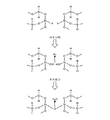
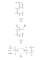
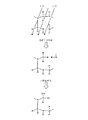
塗布液は、酸化シリコンを含む絶縁膜の前駆体の分子団であるオリゴマーの群を溶媒である溶剤に溶解させて製造される。一般的なキュア工程では、基板を例えば500℃に加熱することにより図1に示すようにオリゴマーのSi−H結合がH2O(水分)との加水分解(反応)により、Si−OHが生成され、続いて脱水縮合(反応)が起こってSi−O−Si結合が生成され、オリゴマー同士が架橋される。The coating liquid is produced by dissolving a group of oligomers, which are molecular groups of precursors of an insulating film containing silicon oxide, in a solvent as a solvent. In a general curing step, when the substrate is heated to, for example, 500 ° C., as shown in FIG. 1, the Si—H bond of the oligomer is hydrolyzed (reacted) with H 2 O (moisture) to generate Si—OH. Then, dehydration condensation (reaction) occurs to form a Si—O—Si bond, and the oligomers are crosslinked.
塗布液の成分としてオリゴマーが用いられる理由は、前駆体全体が連繋されていると溶剤に溶解しないからである。このためオリゴマーの状態、即ち既述の前駆体の加水分解前の状態は安定化しており、加水分解はこの安定化状態から不安定状態に移行させるプロセスであることから、加水分解を促進させるのが難しく、キュア温度を高温化するかあるいは低温で長い時間反応させることが必要になる。 The reason why the oligomer is used as a component of the coating liquid is that if the entire precursor is linked, it does not dissolve in the solvent. Therefore, the state of the oligomer, that is, the state before hydrolysis of the precursor described above is stabilized, and hydrolysis is a process of shifting from this stabilized state to an unstable state, so that hydrolysis is promoted. It is difficult to raise the cure temperature, or it is necessary to react at a low temperature for a long time.
一方脱水縮合反応は熱エネルギーを与えるだけで速やかに進行する。このため加水分解を促進させるためにキュアの温度を高温化すると、加水分解が起こる(Si−HがSi−OHとなる)よりも、脱水縮合が起こる(Si−OHがSi−O−Siとなる)方が容易であることから、絶縁膜の緻密性が低くなる。その理由については、概略的な言い方をすれば、一部のオリゴマー同士が脱水縮合により架橋されたときに、他のオリゴマーは未だ加水分解が行われていない場合が起こり、当該他のオリゴマーが一部のオリゴマー同士の架橋物内に取り込まれてしまうことに起因すると推測される。なお低温で長時間キュアを行う手法は、スループットが低くなるので、生産ラインでは受け入れ難い。 On the other hand, the dehydration condensation reaction proceeds rapidly only by applying thermal energy. Therefore, when the temperature of the cure is raised to promote hydrolysis, dehydration condensation occurs (Si-OH becomes Si-O-Si) rather than hydrolysis occurs (Si-H becomes Si-OH). Since it is easier to do so, the density of the insulating film becomes low. As for the reason, roughly speaking, when some oligomers are crosslinked by dehydration condensation, other oligomers may not have been hydrolyzed yet, and the other oligomers are one. It is presumed that this is due to the fact that the oligomers are incorporated into the crosslinked product. The method of curing at low temperature for a long time is unacceptable on the production line because the throughput is low.
そこで本発明では、キュア工程を行う前に例えば紫外線を塗布膜に照射して、加水分解が起こる部位に未結合手を生成する(オリゴマーをいわば活性化する)ようにしている。即ち図2に示すように紫外線のエネルギーによりオリゴマーにおけるSi−Hの結合を切断して未結合手を生成している。このためキュア工程において加水分解に必要なエネルギーが低くなるので、水酸基(OH基)の生成効率が高くなり、その後の脱水縮合による架橋率が向上する。このことは、低温でキュア工程を行っても、緻密な(良好な膜質である)絶縁膜が得られるということである。 Therefore, in the present invention, for example, the coating film is irradiated with ultraviolet rays before the curing step is performed so as to generate unbonded hands (activate the oligomer, so to speak) at the site where hydrolysis occurs. That is, as shown in FIG. 2, the bond of Si—H in the oligomer is cleaved by the energy of ultraviolet rays to generate an unbonded hand. Therefore, since the energy required for hydrolysis in the curing step is lowered, the efficiency of forming hydroxyl groups (OH groups) is increased, and the cross-linking rate due to subsequent dehydration condensation is improved. This means that a dense (good film quality) insulating film can be obtained even if the curing process is performed at a low temperature.
塗布膜に対する紫外線の照射は、キュア工程の前に行うことが必要である。その理由については、キュア工程は低温とはいっても例えば350℃〜450℃の加熱雰囲気で行われることから、紫外線のエネルギーにより既述のように未結合手が生成されると、未結合手が生成された部位から架橋が起こり、このためSi−H結合が未だ切断されていないオリゴマーが、架橋されたオリゴマー群の中に閉じ込められてしまい、絶縁膜の緻密性が低くなる。 It is necessary to irradiate the coating film with ultraviolet rays before the curing step. The reason is that the curing process is performed in a heating atmosphere of, for example, 350 ° C. to 450 ° C. even though the temperature is low. Crosslinking occurs from the formed site, so that the oligomer in which the Si—H bond has not been cleaved is confined in the crosslinked oligomer group, and the denseness of the insulating film becomes low.
このため紫外線を塗布膜に照射する工程は、このような現象が抑えられた温度で行うことが必要であり、具体的には例えば350℃以下が望ましいと考えられ、例えば室温で行うことができる。また紫外線を塗布膜に照射する工程は、大気雰囲気よりも酸素濃度が低い低酸素濃度雰囲気で行うことが必要であり、例えば酸素濃度が400ppm以下、好ましくは50ppm以下の雰囲気で行われる。低酸素濃度雰囲気は、一例として窒素ガスなどの不活性ガス雰囲気が挙げられる。
この工程が行われる雰囲気において酸素濃度が高いと、紫外線の照射により生成された未結合手を有するオリゴマー同士が瞬時で結合し、結合されたオリゴマーの中に、孤立したオリゴマーが閉じ込められ、結果として絶縁膜の緻密性が低くなる。Therefore, the step of irradiating the coating film with ultraviolet rays needs to be performed at a temperature at which such a phenomenon is suppressed. Specifically, for example, 350 ° C. or lower is considered desirable, and for example, it can be performed at room temperature. .. Further, the step of irradiating the coating film with ultraviolet rays needs to be performed in a low oxygen concentration atmosphere having an oxygen concentration lower than that of the air atmosphere, and is performed in an atmosphere having an oxygen concentration of 400 ppm or less, preferably 50 ppm or less, for example. An example of the low oxygen concentration atmosphere is an atmosphere of an inert gas such as nitrogen gas.
When the oxygen concentration is high in the atmosphere in which this step is performed, oligomers having unbonded hands generated by irradiation with ultraviolet rays are instantly bonded to each other, and isolated oligomers are trapped in the bonded oligomers, resulting in isolation. The denseness of the insulating film is reduced.
[実施の形態]
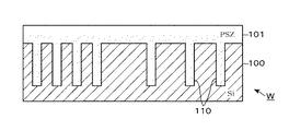
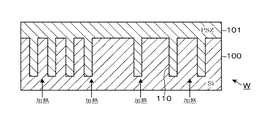
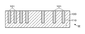
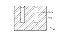
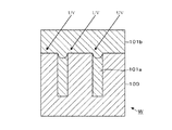
次に本発明の絶縁膜の成膜方法の実施の形態について詳述する。この例では、被処理基板に対してSTIを行うプロセスについて説明する。図3に示すように被処理基板であるウエハWには、シリコン膜100に溝部(トレンチ)110が形成されており、そしてSOG膜の前駆体を有機溶剤に溶解した塗布液をウエハWに塗布することにより、トレンチ110を埋めるように塗布膜101が形成される。前駆体としては、例えば−(SiH2NH)‐を基本構造とするポリマーであるポリシラザンが用いられる。塗布液は、例えば流動性を良くするためにポリシラザンの分子団がオリゴマーの状態で溶解している。そのため図3に示すように、例えばスピンコーティングによりウエハWに塗布したときに塗布液が細いトレンチ110内に進入しやすく埋め込み性の良好な塗布膜101が得られる。なお図3〜図10では、塗布膜101にPSZ(ポリシラザン)と記載している。[Embodiment]
Next, an embodiment of the insulating film forming method of the present invention will be described in detail. In this example, the process of performing STI on the substrate to be processed will be described. As shown in FIG. 3, the wafer W, which is the substrate to be processed, has a
続いて図4に示すようにウエハWを100〜250℃、例えば150℃で3分間加熱する。これにより塗布膜101中に含まれる溶媒である溶剤が揮発する。次に図5に示すようにウエハWを200〜300℃、例えば250℃で加熱する。この時塗布膜101中に含まれるオリゴマーが熱により活性化される。そのため塗布膜101中のオリゴマーが再配列されて、隙間を埋めるように並ぶ(リフロー工程)。このリフロー工程を行いオリゴマーが再配列することによりオリゴマー間の隙間が狭くなる。そのため後段のキュア処理によりオリゴマー同士の架橋を形成したときに緻密な膜になりやすくなる。
Subsequently, as shown in FIG. 4, the wafer W is heated at 100 to 250 ° C., for example, 150 ° C. for 3 minutes. As a result, the solvent, which is the solvent contained in the
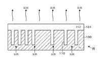
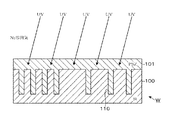
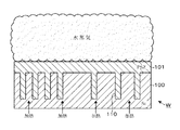
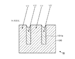
その後、図6に示すように400ppm、好ましくは50ppm以下の酸素濃度の雰囲気、例えば窒素(N2)ガス雰囲気にて、塗布膜101に5000mJ/cm2以下、例えば4000mJ/cm2のエネルギーを照射する。エネルギーとしては、例えば主たる波長が200nm以下の紫外線、例えば主たる波長が172nmの紫外線(UV)を照射する。主たる波長とは、スペクトルにおいて最大ピーク、あるいはその近傍に対応する波長を指している。さらに続くキュア工程においては、図7に示すようにウエハWに向けて水蒸気を供給しながら、350〜450℃の温度にて段階的加熱処理、例えば水蒸気を雰囲気下で400℃と、450℃で段階的に加熱し、さらにN2ガス雰囲気下で450℃で加熱する。Then, 400 ppm as shown in FIG. 6, preferably less oxygen concentration in the
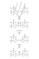
図8は紫外線を照射せずにポリシラザンにキュア処理を行った時の反応経路を示し図9は、紫外線を照射したポリシラザンにキュア処理を行った時の反応経路を示す。図8に示すようにポリシラザンにキュア処理を行うと、加水分解により、Siと結合しているHがOH基となり、さらにN−H基が酸化され、アンモニア(NH3)となることでSi−O結合が形成される。そしてOH基同士が脱水縮合により、架橋を形成していく。しかしながら発明の概要にて述べたようにキュア処理をしたときに加水分解が起こりにくく、緻密性の低い膜となる。FIG. 8 shows the reaction route when the polysilazane was cured without being irradiated with ultraviolet rays, and FIG. 9 shows the reaction route when the polysilazane irradiated with ultraviolet rays was cured. When polysilazane is cured as shown in FIG. 8, the H bonded to Si becomes an OH group by hydrolysis, and the NH group is further oxidized to ammonia (NH 3 ), so that Si- An O bond is formed. Then, the OH groups form crosslinks by dehydration condensation. However, as described in the outline of the invention, hydrolysis is unlikely to occur when the curing treatment is performed, resulting in a film having low density.
これに対してポリシラザンを含む塗布膜101にキュア処理前に紫外線を照射することで、図9に示すようにSi−H結合が切断されて未結合手が形成されると共に、一部のSi−N結合が切断されて未結合手が形成される。これによりキュア処理を行った時に未結合手にOH基が容易に結合し、Si−OHが生成される。また脱水縮合によりOH基同士が架橋し、Si−O−Si結合が形成される。さらにポリシラザンにおけるSi−N結合がOに置換されて酸化シリコンが生成されていく。既述のように予め未結合手を形成することにより、OH基が生成効率が高く、架橋率が向上するため、良好な膜質の絶縁膜(酸化シリコン膜)が形成される。
On the other hand, by irradiating the
絶縁膜が硬化した後、図10に示すようにウエハWは、例えばCMP(chemical Mechanical polishing)によりウエハWの表面の余分な塗布膜101が除去される。この時塗布膜101の強度が低い場合には、CMPによる研磨が難しくなるが、塗布膜101が緻密性が高い酸化シリコン膜となっており、強度が十分に高められているためCMPにより研磨されてウエハWの表面にシリコン膜100が露出する。
After the insulating film is cured, as shown in FIG. 10, in the wafer W, the
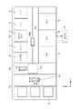
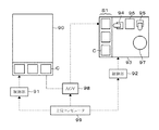
続いて上述の絶縁膜の成膜方法を行うための絶縁膜の成膜装置について説明する。図11、図12に示すように絶縁膜の成膜装置は、ウエハWを複数枚含む搬送容器であるキャリアCから装置内に搬入出するための搬入出ポートであるキャリアブロックS1と、中継ブロックS2と、処理ブロックS3とを一列に接続して構成されている。 Subsequently, an insulating film forming apparatus for performing the above-mentioned insulating film forming method will be described. As shown in FIGS. 11 and 12, the insulating film film forming apparatus includes a carrier block S1 which is an carry-in / out port for carrying in / out from a carrier C which is a transport container containing a plurality of wafers W and a relay block. It is configured by connecting S2 and the processing block S3 in a row.
キャリアブロックS1は、複数枚のウエハWを収納して搬送するためのキャリアCが例えば横方向(X方向)に複数(例えば3個)載置されるステージ11と、ステージ11に載置されたキャリアC内に対してウエハWの受け渡しを行うための搬送アームである受け渡し機構12と、を備えている。受け渡し機構12は、ウエハWの保持部分が進退自在、X方向に移動自在、鉛直軸周りに回転自在、昇降自在に構成されている。
The carrier block S1 is mounted on a
中継ブロックS2は、キャリアブロックS1にてキャリアCから取り出されたウエハWを処理ブロックS3側に受け渡す役割を持っている。中継ブロックS2は、ウエハWの載置台が上下に複数配置された受け渡し棚13と、受け渡し棚13の各載置台の間でウエハWの移載を行うための昇降自在な移載機構14と、を備えている。受け渡し棚13には、処理ブロックS3に設けられる主搬送機構15a、15bがウエハWの受け渡しを行うことができる高さ位置と、受け渡し機構42がウエハWの受け渡しを行うことができる高さ位置と、においてウエハWの載置台が配置されている。
The relay block S2 has a role of delivering the wafer W taken out from the carrier C in the carrier block S1 to the processing block S3 side. The relay block S2 includes a
処理ブロックS3は、上下に処理ブロックB1、B2が積層された2階建てになっている。処理ブロックB1、B2は略同様に構成されており、処理ブロックB1を例に説明する。処理ブロックB1は、各々中継ブロックS2から見て前後方向(Y方向)に伸びる例えばガイドレールからなる搬送路16に沿って移動自在な主搬送機構15aを備えている。処理ブロックB1には、搬送路16の左右両側にウエハWに対して処理を行うためのモジュールが配置されている。処理ブロックB1においては、例えば搬入出ブロックS1から見て右側に、塗布液を塗布するための塗布モジュール2が設けられている。また左側には、中継ブロックS2側から、例えば溶媒揮発モジュール3、リフローモジュール4、紫外線照射モジュール5及び2台のキュアモジュール6が並んで配置されている。
The processing block S3 has a double-decker structure in which the processing blocks B1 and B2 are laminated one above the other. The processing blocks B1 and B2 are configured in substantially the same manner, and the processing block B1 will be described as an example. Each of the processing blocks B1 includes a
また絶縁膜の成膜装置には、例えばコンピュータからなる制御部9が設けられている。制御部9は、プログラム格納部を有しており、プログラム格納部には、成膜装置内におけるウエハWの搬送、あるいは各モジュールにおけるウエハWの処理のシーケンスが実施されるように命令が組まれた、プログラムが格納される。このプログラムは、例えばフレキシブルディスク、コンパクトディスク、ハードディスク、MO(光磁気ディスク)、メモリーカードなどの記憶媒体により格納されて制御部8にインストールされる。 Further, the insulating film film forming apparatus is provided with a control unit 9 including, for example, a computer. The control unit 9 has a program storage unit, and the program storage unit is instructed to carry out a transfer of the wafer W in the film forming apparatus or a sequence of processing the wafer W in each module. Also, the program is stored. This program is stored in a storage medium such as a flexible disk, a compact disk, a hard disk, an MO (magneto-optical disk), or a memory card, and is installed in the control unit 8.
絶縁膜の成膜装置におけるウエハWの流れを簡単に説明すると、ウエハWを収納したキャリアCがステージ11載置されると、受け渡し機構12、受け渡し棚13及び移載機構14を介して処理ブロックB1又はB2に搬送される。その後、ウエハWは、塗布モジュール2にて塗布膜101が塗布され、溶媒揮発モジュール3→リフローモジュール4→紫外線照射モジュール5→キュアモジュール6の順番に搬送されて絶縁膜が形成される。その後ウエハWは、受け渡し棚13に受け渡され、移載機構14及び受け渡し機構12によりキャリアCに戻される。
なお絶縁膜の成膜装置は、CMPを行う研磨装置を備えてもよく、例えば一方のキュアモジュール6に代えて研磨装置を設けてもよい。そしてキュアモジュール6にてキュア処理を行った後のウエハWをCMPにより研磨するように構成してもよい。To briefly explain the flow of the wafer W in the insulating film film forming apparatus, when the carrier C accommodating the wafer W is placed on the
The insulating film film forming apparatus may be provided with a polishing apparatus for performing CMP. For example, a polishing apparatus may be provided instead of one of the
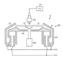
続いて、塗布モジュール2について説明する。塗布モジュール2は例えばパターンの形成されたウエハWに対して、公知のスピンコーティング法により、絶縁膜の前駆体となるポリシラザンを有機溶剤に溶解した塗布液を塗布する。塗布モジュール2は、図13に示すようにウエハWを吸着保持して駆動機構22により回転自在、昇降自在に構成されたスピンチャック21を備えている。また図13中の23はカップモジュールである。図13中24は、下方に伸びる外周壁及び内周壁が筒状に形成されたガイド部材である。
Subsequently, the
また外カップ25と前記外周壁との間には、排出空間が形成され、排出空間の下方は、気液分離できる構造になっている。ガイド部材24の周囲には、外カップ25の上端から中心側に向かって伸び出すように設けられた、ウエハWから振り切られた液を受け止める液受け部27が設けられている。また塗布ユニット2は塗布液ノズル28を備え、例えばポリシラザンなどの塗布液が貯留された塗布液供給源29から塗布液ノズル28を介してウエハWの中心部に塗布液を供給すると共にウエハWを鉛直軸周りに所定の回転数で回転させ、ウエハWの表面に塗布液を展伸して塗布膜を形成する。
Further, a discharge space is formed between the
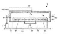
次に溶媒揮発モジュール3について説明する。図14に示すように溶媒揮発モジュール3は、図示しない筐体内に上面が開口している扁平な円筒体からなる下部材31と、この下部材31に対して上下に移動して処理容器2を開閉する蓋部32とからなる処理容器30を備えている。下部材32は筐体の底面部3aに支持部材41を介して支持されている。また下部材31にはウエハWを載置して、例えば100〜250℃に加熱するための加熱機構34が埋設された加熱板33が設けられている。筐体の底面部3aには、下部材25の底部及び加熱板21を貫通しウエハWを外部の主搬送機構15aとの間で受け渡しを行うための昇降ピン35を昇降させるための昇降機構36が設けられている。
Next, the
蓋部32は下面が開口している扁平な円筒体からなり、蓋部32の天井板の中央部には、排気口38が形成され、この排気口38には排気管39が接続されている。この排気管39は処理容器30側を上流側とすると、工場内に引き回されている共用の排気ダクトにその下流端が接続されている。
The
蓋部32は、下部材31の周壁部の上面に設けられたピン40に接触するように載置され、蓋部32と下部材との間にわずかな隙間が形成されるように載置され、ウエハWを加熱する処理空間を形成する。そして排気口38から排気を行うことにより、筐体内の雰囲気が蓋部32と、下部材25と隙間から処理容器内に流入するように構成されている。また蓋部32には、蓋部32を処理容器2を閉じた状態とする下降位置と、ウエハWを加熱板21に対して受け渡すときの上昇位置との間で昇降できるように構成されている。この例では蓋部22の昇降動作は蓋部22の外周面に取り付けられた昇降機構37を駆動することにより行われる。
またリフローモジュール4は、加熱機構34により、ウエハWが200〜300℃に加熱するように構成されたことを除いて溶媒揮発モジュール3とほぼ同様に構成されている。The
Further, the reflow module 4 is configured in substantially the same manner as the
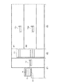
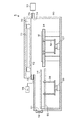
エネルギー供給モジュールである紫外線照射モジュール5は、図15に示すように扁平で前後方向に細長い直方体形状の筐体50を備え、筐体50の前方側の側壁面にはウエハWを搬入出するための搬入出口51と、この搬入出口51を開閉するシャッタ52とが設けられている。
筐体50の内部は、搬入出口51から見て手前側にウエハWを搬送する搬送アーム53が設けられている。搬送アーム53は、クーリングプレートとして構成され、例えばリフロー工程後、紫外線照射処理の前に、ウエハWを常温(25℃)まで冷却できるように構成されている。搬入出口71から見て奥側には、ウエハWの載置台54が配置されている。載置台54及び搬送アーム53の下方にはウエハの受け渡しを行うための昇降ピン56、58が夫々設けられ、昇降ピン56、58は、夫々昇降機構57、59により昇降するように構成されている。As shown in FIG. 15, the
Inside the
載置台54の上方側には、載置台54に載置されたウエハWに紫外線光を照射するための例えば主たる波長が172nmの紫外線を照射するキセノンランプなどの紫外線ランプ71を収容したランプ室70が設けられている。ランプ室70の下面は、紫外線ランプ71から照射された波長172nmの紫外線光をウエハWへ向けて透過させる光透過窓72が設けられている。またランプ室70の下方の側壁には、ガス供給部73と、排気口74と、が互いに対向するように設けられている。ガス供給部73には、筐体50内にN2ガスを供給するためのN2ガス供給源75が接続されている。排気口74には、排気管76を介して排気機構77が接続されている。
そして載置台54に載置されたウエハWに紫外線を照射するときには、ガス供給部73からN2ガスを供給すると共に排気を行い、ウエハWの雰囲気を例えば400ppm以下より好ましくは50ppm以下の低酸素雰囲気、例えばN2ガス雰囲気とするように構成されている。搬送アームに53にて常温まで冷却されたウエハWが載置台54に載置されると、N2ガス供給源75からN2ガスを供給し、低酸素雰囲気とした状態でウエハWに例えば4000mJ/cm2のエネルギーが照射されるOn the upper side of the mounting table 54, a
And when irradiated with ultraviolet rays to the wafer W mounted on the mounting table 54, performs an exhaust supplies the N 2 gas from the
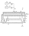
続いてキュアモジュール6について説明する。図16に示すようにキュアモジュール6は、図示しない筐体内に蓋部62及び下部材61とで構成される処理容器60を設けて構成される。処理容器60内には、ウエハWが載置される載置台63が設けられ、載置台63には、載置台63に載置されたウエハWを例えば350〜450℃に加熱する加熱機構65が設けられている。また蓋部62の天板部にはガス導入口65が設けられ、ガス導入口65には、ガス供給管66の一端が接続されている。ガス供給管66の他端側は、2本に分岐し、一方の端部には、処理容器60内に水蒸気を供給するための水蒸気供給源67が接続され、もう一方の端部には、処理容器60内にN2ガスを供給するためのN2ガス供給源68が接続されている。なお図16中のV67、V68はバルブであり、M67、M68は、流量調整部である。Subsequently, the
また蓋部62におけるガス導入口65の下方には、載置台63の上面と対向するようにガス拡散板69が設けられている。ガス拡散板69は例えばパンチングプレートで構成され、ガス導入口65から処理容器60内に導入されたガスを拡散し、載置台63に載置されたウエハWに向けて供給する。また下部材61には、排気口82が形成され、排気口には、排気管83の一端が接続されると共に、排気管83の他端側は排気部に接続されている。
Further, below the
蓋部62は、筐体の底面部に設置された昇降機構81により昇降するように構成され、蓋部62を上昇させた状態でウエハWが処理容器60内に搬入されて載置台63に載置される。そして蓋部62を下降させることで処理容器60が密閉され、載置台63に載置されたウエハWを加熱しながら水蒸気を供給するための処理空間が形成される。
そして既述のように紫外線照射処理を行ったウエハWが載置台63に載置されると、処理容器60内に水蒸気を満たすと共にウエハWを400℃で30分、450℃で120分段階的に加熱した後、水蒸気の供給を停止し、窒素ガス雰囲気下で450℃で30分加熱する。The
Then, when the wafer W subjected to the ultraviolet irradiation treatment as described above is placed on the mounting table 63, the
上述の実施の形態によれば、ポリシラザンを含む塗布液をウエハWに塗布し、塗布膜101中の溶剤を揮発させた後、キュア工程を行う前に、窒素雰囲気で前記塗布膜101に紫外線を照射している。このためポリシラザンにおける加水分解される部位にて未結合手が生成されやすい。そのため予め加水分解される部位であるシリコンに未結合手を生成していることから、水酸基の生成効率が高くなる。即ち、加水分解に必要なエネルギーが低下することから、キュア工程の温度を350℃としたときにも、加水分解されずに残る部位が少なくなる。この結果効率的に脱水縮合が起こるので、架橋率が向上して緻密な(良質な膜質である)絶縁膜を成膜することができる。
According to the above-described embodiment, after the coating liquid containing polysilazane is applied to the wafer W and the solvent in the
また本発明は、塗布処理から紫外線照射の工程までを行う成膜装置と、別個にキュア処理を行う熱処理装置とを備え、成膜装置で紫外線照射を行ったウエハWを、熱処理装置に搬送してキュア処理を行う基板処理システムであってもよい。図17に示すように基板処理システムは、キュア処理装置を設けないことを除いて、図11、図12に示す絶縁膜の成膜装置と同様に構成した基板処理装置90と、ウエハWに熱処理を行う熱処理炉97を含む熱処理装置93と、を備え、基板処理装置90と熱処理装置93との間においてキャリアCを搬送する容器搬送機構である搬送車(AVG)98が設けられている。熱処理装置93は、キャリアCが搬送されるキャリアブロックS1と、キャリアCからウエハを取り出す受け渡し機構94とキャリアCから取り出したウエハWを載置する載置棚96と、載置棚96に載置されたウエハWを熱処理炉97に移載する移載機構95を備えている。熱処理炉97は、例えば周知の熱処理炉が用いられ、複数枚の基板を基板保持具に棚状に配置してヒータで囲まれた縦型の反応管内に搬入して熱処理(キュア)が行われる。
Further, the present invention includes a film forming apparatus that performs the steps from coating treatment to ultraviolet irradiation, and a heat treatment apparatus that separately performs curing treatment, and the wafer W that has been irradiated with ultraviolet rays by the film forming apparatus is conveyed to the heat treatment apparatus. It may be a substrate processing system that performs a curing process. As shown in FIG. 17, the substrate processing system heat-treats the
そしてこの基板処理システムは、基板処理装置90の制御部91と、熱処理装置93におけるウエハWの搬送及びキュア処理工程を実行するためのプログラムを備えた熱処理装置93の制御部92と、に制御信号を送信すると共に、搬送車98によるキャリアCの搬送を制御する上位コンピュータ99を備えている。上位コンピュータ99には、既述の絶縁膜の成膜方法を実行するためのプログラムが記憶されており、ウエハWへの塗布液の塗布から紫外線照射処理までの工程を基板処理装置90にて行い、紫外線を照射したウエハWをキャリアCに収納して、搬送車98により熱処理装置93に搬送し、キュア処理を行う。このような基板処理システムにおいても同様に絶縁膜の成膜方法を適用することができる。このように熱処理炉を含む基板処理システムを用いても強度の高い絶縁膜を成膜することができる効果がある。一方でキュア処理工程の温度が低くできるため、絶縁膜成膜工程を行うにあたって、高温処理を行うための専用の熱処理炉を含む基板処理システムとする必要がない効果もある。
Then, this substrate processing system sends a control signal to the
さらに上述の実施の形態において、キュア工程において、アンモニアガスを供給しながら加熱してキュア処理を行うようにしてもよい。あるいはキュア処理の際に供給するガスはN2ガスであってもよい。
また本発明は、低誘電率膜などの層間絶縁膜の成膜に適用してもよい。層間絶縁膜の成膜にあたっては、配線材料である銅のマイグレーションや拡散を抑えるために、加熱温度は、450℃以下、例えば400℃以下にすることが要請されている。また層間絶縁膜を十分な硬度に構成する観点から300℃以上出ることが好ましい。本発明ではキュア温度が低温であっても良質な膜質の絶縁膜が得られることから、層間絶縁膜の成膜に適用することが期待できる。また例えば細い溝部が形成された基板に絶縁膜を形成する例としてPMD(Pre Metal Dielectric)に適用してもよい。Further, in the above-described embodiment, in the curing step, the curing treatment may be performed by heating while supplying ammonia gas. Alternatively, the gas supplied during the curing treatment may be N 2 gas.
Further, the present invention may be applied to the film formation of an interlayer insulating film such as a low dielectric constant film. In forming the interlayer insulating film, the heating temperature is required to be 450 ° C. or lower, for example 400 ° C. or lower, in order to suppress migration and diffusion of copper as a wiring material. Further, from the viewpoint of forming the interlayer insulating film with sufficient hardness, it is preferable that the temperature is 300 ° C. or higher. In the present invention, since an insulating film having a high quality film quality can be obtained even when the curing temperature is low, it can be expected to be applied to the film formation of an interlayer insulating film. Further, for example, it may be applied to PMD (Pre Metal Dielectric) as an example of forming an insulating film on a substrate on which a narrow groove portion is formed.
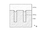
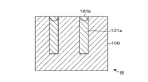
また本発明は、塗布液を複数回塗布して絶縁膜を成膜するようにしても良い。例えば図11、図12に示す絶縁膜の成膜装置において、まずトレンチ110が形成されたウエハWを塗布モジュール2に搬送して、一回目の塗布液の塗布を行う。これにより例えば図18に示すようにシリコン膜100に形成されたトレンチ110の内部に塗布液が進入した状態の塗布膜101aが形成される。なお図18〜図23では、1回目の塗布液の塗布により形成される塗布膜を101aで示し、2回目の塗布液の塗布により形成される塗布膜を101bで示す。
Further, in the present invention, the coating liquid may be applied a plurality of times to form an insulating film. For example, in the insulating film film forming apparatus shown in FIGS. 11 and 12, the wafer W on which the
その後ウエハWを、実施の形態と同様に溶媒揮発モジュール3に搬送し、溶剤を揮発させた後、例えば紫外線照射モジュール5に搬送し、図19に示すように低酸素雰囲気にて塗布膜101aに紫外線を照射する。次いでウエハWを塗布モジュール2に搬送し、2回目の塗布処理を行う。これにより図20に示すようにウエハWに、さらに塗布膜101bが積層される。その後ウエハWを溶媒揮発モジュール3に搬送し、溶剤を揮発させた後、紫外線照射モジュール5に搬送し、図21に示すように低酸素雰囲気にて塗布膜101bに紫外線を照射する。続いてウエハWをキュアモジュール6に搬送し、図22に示すように例えば水蒸気雰囲気下で400℃、450℃で段階的に加熱した後N2ガス雰囲気下で450℃に加熱する。その後例えばウエハWをCMP装置に搬送し、図23に示すように表層の塗布膜101bをCMPにより除去する。After that, the wafer W is transferred to the
塗布膜101a、101bに紫外線を照射したときに、紫外線は塗布膜101a、101bの表層側から下層側に透過していくため、塗布膜101a、101bの下層側は表層側に比べて、紫外線が弱まりやすく、Si−H結合が十分に未結合手にならないおそれがある。そのためウエハWにキュア処理を行った時に塗布膜101a、101bの下層側において、架橋率が低くなることがあり、膜全体としての架橋率が低くなることがある。また例えば表層の塗布膜をCMPにより除去したときに塗布膜における膜質の悪い層が露出するおそれがある。
When the
そのため塗布膜101a、101bの塗布と、紫外線照射とを複数回繰り返して所定の膜厚の塗布膜101a、101bを成膜することで、塗布膜101a、101bが各々薄い状態で紫外線照射処理ができ、塗布膜101a、101bの全層に、未結合手が形成されやすくなる。そのためキュア処理を行った時に塗布膜101a、101bの全層で、架橋が形成されやすくなり、全層に亘って架橋率が高く緻密な塗布膜101a、101bを形成することができる。これにより後述の実施例2に示すようにより緻密でエッチング強度の高い絶縁膜を成膜することができる。
Therefore, by repeating the coating of the
また1回目の塗布処理を行い、溶剤を揮発させ、低酸素雰囲気にて塗布膜101aに紫外線を照射した後に、さらにキュアモジュール6に搬送し、例えば水蒸気雰囲気下で350℃に加熱してもよい。その後2回目の塗布処理を行い、溶剤を揮発させた後、低酸素雰囲気にて塗布膜101bに紫外線を照射し、さらにキュア処理を行ってもよい。
さらに1回目の塗布処理及び2回目の塗布処理における溶剤を揮発させた後に、例えばウエハWを250℃で加熱するリフロー工程を行うようにしてもよい。Further, the first coating treatment may be performed to volatilize the solvent, the
Further, after volatilizing the solvent in the first coating treatment and the second coating treatment, for example, a reflow step of heating the wafer W at 250 ° C. may be performed.
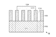
また本発明は、例えば犠牲膜を成膜する工程に適用してもよい。図24は、犠牲膜を形成した被処理基板の一例を示す。図24に示すようにウエハWは、SiO2膜102の上面にポリシリコン層103が形成され、さらにポリシリコン層103を厚さ方向に貫通するようにトレンチ110が形成されている。そしてこのウエハWの上面に犠牲膜となるSiON膜104が成膜される。図24は、SiON膜104を成膜した後、所定のパターンでSiON膜104をエッチングした後のウエハWの表層部の断面の様子を示している。このウエハWにおいては、SiON膜104及びポリシリコン層103に対するSiO2層102のエッチング選択比を利用して、SiON膜104でおおわれておらず、SiON膜104の除去されたトレンチ110の底部に臨むSiO2層102をエッチングする。Further, the present invention may be applied to, for example, a step of forming a sacrificial film. FIG. 24 shows an example of the substrate to be processed on which the sacrificial film is formed. As shown in FIG. 24, in the wafer W , a polysilicon layer 103 is formed on the upper surface of the SiO 2 film 102, and a
SiON膜104などの犠牲膜は、回路パターンなどの凹凸が形成されたウエハWに成膜されることから、埋め込み性が良好であることが好ましい。そのため塗布液の塗布により成膜されることが好ましい。またエッチング対象となる膜ここではSiO2膜102とのエッチング選択比を十分に高めることからエッチング強度が高いことが好ましい。
SiON膜104を成膜するにあたっては、例えば前駆体としてポリシラザンを含んだ塗布液をウエハWに向けて塗布する。その後図3〜図6に示したように、塗布膜101を例えば150℃で3分加熱して塗布膜101中の溶剤を揮発させた後、250℃で加熱して塗布膜101のリフローを行う。次いで塗布膜101に向けて、低酸素雰囲気下で5000J/cm2以下の紫外線を照射する。その後、キュアモジュール6において、N2ガス雰囲気下でウエハWを400℃、450℃で段階的に加熱するキュア工程を行う。Since the sacrificial film such as the
In forming the
前駆体として含まれるポリシラザンにおいては、上述のように塗布膜101中に含まれるオリゴマー同士の脱水縮合を進めるときに、ポリシラザンに含まれる−Si(NH)Si−がSi−O−Si結合に置換される。この−Si(NH)Si−からSi−O−Si結合への置換率が高いとSiO2に近づき、−Si(NH)Si−をより多く残すように成膜することでN濃度が高いSiON膜になる。従って塗布膜101に紫外線を照射した後、キュア工程において、例えばN2ガス雰囲気下で350℃に加熱する。この時低い温度、例えば350〜450℃キュア処理をすることで、−Si(NH)Si−の置換が抑制された状態となると共に、紫外線の照射により形成された未結合手が、既述のように加水分解及び脱水縮合を行いSi−O−Si結合の生成が進行する。従ってポリシラザンのオリゴマーを架橋させて強固な膜とすると共に、窒素の離脱を抑え、窒素含有率が高いSiON膜を成膜することができる。In polysilazane contained as a precursor, -Si (NH) Si- contained in polysilazane is replaced with a Si-O-Si bond when advancing dehydration condensation between oligomers contained in the
また紫外線を照射する工程において、架橋が進行する温度、例えばポリシラザンでは、350〜400℃まで上げてしまうと、未結合手の形成と、加水分解及び脱水縮合と、が同時に進行してしまうことがあり、結合されたオリゴマーの中に、孤立したオリゴマーが閉じ込められ、結果として絶縁膜の緻密性が低くなる。
そのため紫外線を照射する温度は、350℃以下であることが好ましい。また紫外線照射時に架橋の進行しない温度であることが要件であることから、リフロー工程において紫外線を照射するようにしてもよい。しかしながら溶剤揮発工程においては、溶媒である溶剤が紫外線の照射により変質するおそれもある。そのため、溶剤揮発工程以後である必要がある。Further, in the step of irradiating ultraviolet rays, if the temperature at which cross-linking proceeds, for example, polysilazane, is raised to 350 to 400 ° C., the formation of unbonded hands and hydrolysis and dehydration condensation may proceed at the same time. Yes, isolated oligomers are trapped in the bonded oligomers, resulting in less compactness of the insulating film.
Therefore, the temperature for irradiating ultraviolet rays is preferably 350 ° C. or lower. Further, since it is a requirement that the temperature is such that cross-linking does not proceed when irradiated with ultraviolet rays, ultraviolet rays may be irradiated in the reflow process. However, in the solvent volatilization step, the solvent as a solvent may be deteriorated by irradiation with ultraviolet rays. Therefore, it is necessary to be after the solvent volatilization step.
またエネルギー照射工程におけるエネルギーが大きすぎると、Si−H結合以外の他の結合が切断されてしまうことがある。そのためエネルギーの照射量は、5000J/cm2以下であることが好ましく、Si−H結合の末端を切るのに十分なドーズ量以上の照射量であればよい。Further, if the energy in the energy irradiation step is too large, bonds other than the Si—H bond may be broken. Therefore, the irradiation amount of energy is preferably 5000 J / cm 2 or less, and the irradiation amount may be a dose amount or more sufficient to cut the end of the Si—H bond.
また後述の実施例3に示すように溶剤揮発工程におけるウエハWの加熱温度を200〜250℃にして上述の絶縁膜の成膜方法を実行することで効果を上げることができる。これは、塗布膜101中の溶剤をより確実に除去することで、溶剤に吸収されるエネルギーは少なくなるためと、実施例3ではリフロー処理を行っておらず、リフロー処理におけるオリゴマーの再配列に相当する効果生じたためと、の相乗効果であると推測される。
Further, as shown in Example 3 described later, the effect can be improved by carrying out the above-mentioned film forming method of the insulating film by setting the heating temperature of the wafer W in the solvent volatilization step to 200 to 250 ° C. This is because the energy absorbed by the solvent is reduced by removing the solvent in the
また効率よく未結合手を形成する観点から、塗布膜を透過せず、塗布膜に吸収される波長のエネルギーが好ましい。そのため紫外線の場合には、主たる波長が200nm以下であることが好ましく、例えばArFランプなどの波長193nmの紫外線を用いてもよく、また重水素ランプなどを用いてもよい。さらに塗布膜に照射するエネルギーとしては、電子線などを用いてもよい。
また溶剤揮発工程に用いる塗布膜101中の溶剤を揮発させる装置は、例えば密閉した処理容器内を例えば大気圧の半分まで減圧し、処理容器内に載置したウエハWにおける溶剤の揮発を促進して溶剤を揮発させる装置でも良い。Further, from the viewpoint of efficiently forming unbonded hands, energy having a wavelength that does not pass through the coating film and is absorbed by the coating film is preferable. Therefore, in the case of ultraviolet rays, the main wavelength is preferably 200 nm or less, and for example, ultraviolet rays having a wavelength of 193 nm such as an ArF lamp may be used, or a deuterium lamp or the like may be used. Further, as the energy to irradiate the coating film, an electron beam or the like may be used.
Further, the device for volatilizing the solvent in the
<評価試験1>
本発明の実施の形態の効果を検証するために以下の試験を行った。図17に示した基板処理システムを用い、評価用のウエハWに絶縁膜を成膜し、絶縁膜のエッチング強度について評価した。
[実施例1]
絶縁膜の成膜方法における紫外線照射工程においてN2ガス雰囲気下で主たる波長が172nmの紫外線をドーズ量が2000mJ/cm2となるように照射した例を実施例1−1とした。なおウエハWは、実施の形態に示した塗布液を塗布した後、溶剤揮発工程において、ウエハWを150℃で3分加熱し、その後リフロー工程を行わずに、紫外線照射工程を行った。続くキュア工程においては、熱処理炉内において、水蒸気を供給した状態で、400℃で30分、450℃で120分の2段階の加熱を行った後、N2ガス雰囲気下で450℃で30分加熱した。なお塗布膜の目標膜厚は100nmとした。
[比較例1、2]
また紫外線照射工程において、大気雰囲気にて2000mJ/cm2の紫外線を照射したことを除いて、実施例1−1と同様に処理した例を比較例1とした。また紫外線照射を行わないことを除いて、実施例1−1と同様に処理した例を比較例2とした。<
The following tests were conducted to verify the effect of the embodiments of the present invention. Using the substrate processing system shown in FIG. 17, an insulating film was formed on the evaluation wafer W, and the etching strength of the insulating film was evaluated.
[Example 1]
Principal wavelength under N 2 gas atmosphere in the ultraviolet irradiation step in the film forming method of the insulating film was irradiated Examples Example 1-1 to a dose of ultraviolet radiation of 172nm is 2000 mJ / cm 2. After applying the coating liquid shown in the embodiment, the wafer W was heated at 150 ° C. for 3 minutes in the solvent volatilization step, and then the ultraviolet irradiation step was performed without performing the reflow step. In the subsequent curing step, in the heat treatment furnace, while supplying water vapor, 30 minutes at 400 ° C., after two-stage heating of 120 minutes at 450 ° C., 30 minutes at 450 ° C. under a N 2 gas atmosphere Heated. The target film thickness of the coating film was set to 100 nm.
[Comparative Examples 1 and 2]
Further, in the ultraviolet irradiation step, Comparative Example 1 was treated in the same manner as in Example 1-1 except that the ultraviolet rays of 2000 mJ / cm 2 were irradiated in the atmospheric atmosphere. In addition, Comparative Example 2 was an example of treatment in the same manner as in Example 1-1 except that ultraviolet irradiation was not performed.
実施例1、比較例1、2の各々において、0.5%希フッ酸によりウェットエッチングを行い単位時間当たりのエッチング量(エッチングレート)を評価し、0.5%希フッ酸に対するシリコンの熱酸化膜のエッチングレートを1としたときの各々の例における相対的エッチングレートを求めた。以下実施例においては、この相対的エッチングレートによりエッチング強度を評価した。
比較例1、2における相対的エッチングレートは、夫々3.74、5.55であった。これに対して、実施例1における相対的エッチングレートは、2.04であった。
この結果によれば、ポリシラザンを含む塗布液をウエハWに塗布し絶縁膜を成膜するにあたって、キュア工程前の塗布膜にN2ガス雰囲気下で紫外線のエネルギーを照射することにより、エッチング強度を高めることができるといえる。In each of Example 1 and Comparative Examples 1 and 2, wet etching was performed with 0.5% dilute hydrofluoric acid, the etching amount (etching rate) per unit time was evaluated, and the heat of silicon with respect to 0.5% dilute hydrofluoric acid was evaluated. The relative etching rate in each example was determined when the etching rate of the oxide film was 1. In the following examples, the etching strength was evaluated by this relative etching rate.
The relative etching rates in Comparative Examples 1 and 2 were 3.74 and 5.55, respectively. On the other hand, the relative etching rate in Example 1 was 2.04.
According to this result, when forming the coating composition was coated on the wafer W insulating film containing polysilazane by irradiating the UV energy in N 2 gas atmosphere in the coating film before curing process, the etching strength It can be said that it can be enhanced.
さらに実施例1及び比較例1の各々において、(FT−IR:フーリエ変換赤外分光光度計)を用い、紫外線照射処理の前後及びキュア処理後における原子結合の量を評価した。比較例1においては、紫外線照射処理の後において、Si−H結合が減少し、Si−O結合が増加していた。また実施例1においては、紫外線照射処理の後にSi−H結合の減少は見られたが、Si−O結合は増加しておらず、キュア処理後においてSi−O結合が増加していた。 Further, in each of Example 1 and Comparative Example 1, (FT-IR: Fourier transform infrared spectrophotometer) was used to evaluate the amount of atomic bonds before and after the ultraviolet irradiation treatment and after the cure treatment. In Comparative Example 1, the Si—H bond decreased and the Si—O bond increased after the ultraviolet irradiation treatment. Further, in Example 1, although a decrease in Si—H bond was observed after the ultraviolet irradiation treatment, the Si—O bond did not increase, and the Si—O bond increased after the cure treatment.
この結果から推測すると、紫外線照射処理をすることによりSi−H結合が減少しており、未結合手を形成することができるが、紫外線照射処理を大気雰囲気で行うと、キュア処理に先立って、架橋反応が進行し、紫外線照射処理をN2ガス雰囲気下で行うと、キュア処理前の架橋反応抑制できると考えられる。そしてキュア処理前に未結合手を形成すると共に、架橋反応を抑制することにより、エッチング強度が高まると推測される。
また紫外線をドーズ量を3000及び4000mJ/cm2に設定した場合において、相対的エッチングレートを評価したところ各々2.70.2.42であり、4000mJ/cm2程度の紫外線のドーズ量においても強度の高い絶縁膜を得ることができた。Inferring from this result, the Si—H bond is reduced by the ultraviolet irradiation treatment, and unbonded hands can be formed. However, when the ultraviolet irradiation treatment is performed in an air atmosphere, prior to the cure treatment, crosslinking reaction proceeds, when the ultraviolet irradiation treatment under N 2 gas atmosphere, believed to be the pre-cure treatment crosslinking reaction suppression. It is presumed that the etching strength is increased by forming unbonded hands before the curing treatment and suppressing the cross-linking reaction.
Further, when the dose amount of ultraviolet rays was set to 3000 and 4000 mJ / cm 2 , the relative etching rates were evaluated to be 2.70.2.42, respectively, and the intensity was also high even at the dose amount of ultraviolet rays of about 4000 mJ / cm 2. We were able to obtain a high-quality insulating film.
<評価試験2>
またウエハWへの塗布液の塗布と、塗布膜への紫外線照射処理と、を複数回繰り返した後、キュア処理を行うことの効果を検証するため、以下の実施例に従って図17に示した基板処理システムを用い、ウエハWに絶縁膜を成膜し、実施例1と同様に相対的エッチングレートを求め、絶縁膜のエッチング強度について評価した。
[実施例2−1]
評価用のウエハWに1回目の塗布液を塗布した後、溶剤揮発工程において、ウエハWを150℃で3分加熱し、その後リフロー工程を行わずに、実施の形態と同様に紫外線照射工程を行った。紫外線照射工程においてN2ガス雰囲気下で照射する波長172nmの紫外線のドーズ量を4000mJ/cm2に設定した。さらに2回目の塗布液の塗布として、1回目の塗布液と同量の塗布液を塗布した後、溶剤揮発工程において、ウエハWを150℃で3分加熱し、その後リフロー工程を行わずに、実施の形態と同様に紫外線照射工程を行った。その後実施例1と同様のキュア工程を行った例を実施例2−1とした。なお1回目の塗布液を塗布及び2回目の塗布液の塗布における塗布液の供給量は、凡そ実施例1と同様であり、キュア処理後の塗布膜の目標膜厚は200nmとした。<
Further, in order to verify the effect of performing the curing treatment after repeating the coating of the coating liquid on the wafer W and the ultraviolet irradiation treatment of the coating film a plurality of times, the substrate shown in FIG. 17 according to the following embodiment. An insulating film was formed on the wafer W using a processing system, the relative etching rate was obtained in the same manner as in Example 1, and the etching strength of the insulating film was evaluated.
[Example 2-1]
After applying the first coating liquid to the evaluation wafer W, in the solvent volatilization step, the wafer W is heated at 150 ° C. for 3 minutes, and then the ultraviolet irradiation step is performed in the same manner as in the embodiment without performing the reflow step. went. In the ultraviolet irradiation step, the dose amount of ultraviolet rays having a wavelength of 172 nm irradiated in an N 2 gas atmosphere was set to 4000 mJ / cm 2. Further, as the second application of the coating liquid, after applying the same amount of the coating liquid as the first coating liquid, the wafer W is heated at 150 ° C. for 3 minutes in the solvent volatilization step, and then the reflow step is not performed. The ultraviolet irradiation step was carried out in the same manner as in the embodiment. After that, an example in which the same curing step as in Example 1 was performed was referred to as Example 2-1. The amount of the coating liquid supplied in the first coating liquid coating and the second coating liquid coating was approximately the same as in Example 1, and the target film thickness of the coating film after the cure treatment was set to 200 nm.
[実施例2−2]
塗布液の塗布量を実施例1の凡そ2倍の量として、塗布膜の目標膜厚を200nmとして成膜し、紫外線照射工程においてN2ガス雰囲気下で照射する波長172nmの紫外線のドーズ量を4000mJ/cm2に設定したことを除いて、実施例1と同様に処理した例を実施例2−2とした。
実施例2−1及び2−2における相対的エッチングレートは、夫々2.27、2.56であった。実施例2−1及び2−2のいずれにおいても相対的エッチングレートが低くなっており、エッチング強度が高いことが分かる。また実施例2−2と比較して、実施例2−1はさらに相対的エッチングレートが低くなっていることが分かる。
この結果によれば、ウエハWへの塗布液の塗布と、塗布膜への紫外線照射処理と、を複数回繰り返すことにより、より緻密で良好な絶縁膜を得ることができると言える。[Example 2-2]
The coating amount of the coating liquid as the amount of approximately 2-fold in Example 1, was deposited a target thickness of the coating film as 200 nm, the dose of ultraviolet radiation of wavelength 172nm is irradiated under N 2 gas atmosphere in the ultraviolet irradiation step An example of processing in the same manner as in Example 1 except that it was set to 4000 mJ / cm 2 was designated as Example 2-2.
The relative etching rates in Examples 2-1 and 2-2 were 2.27 and 2.56, respectively. It can be seen that the relative etching rate is low and the etching strength is high in both Examples 2-1 and 2-2. Further, it can be seen that the relative etching rate of Example 2-1 is further lower than that of Example 2-2.
According to this result, it can be said that a denser and better insulating film can be obtained by repeating the coating of the coating liquid on the wafer W and the ultraviolet irradiation treatment of the coating film a plurality of times.
<評価試験3>
また溶剤揮発工程におけるウエハWの加熱温度による効果を検証するため、以下の実施例に従って図17に示した基板処理システムを用い、ウエハWに絶縁膜を成膜し、絶縁膜のエッチング強度について評価した。
[実施例3−1]
ウエハWは、実施の形態に示した塗布液を塗布した後、溶剤揮発工程において、ウエハWを150℃で3分加熱し、その後リフロー工程を行わずに、紫外線照射工程を行った。続くキュア工程においては、熱処理炉内において、水蒸気を供給した状態で、400℃で30分、450℃で120分の2段階の加熱を行った後、N2ガス雰囲気下で450℃で30分加熱した。なお塗布膜の目標膜厚は100nmとした。
[実施例3−2、3−3]
溶剤揮発工程におけるウエハWの加熱温度を200℃、250℃に設定したことを除いて実施例3−1と同様に処理した例を、夫々実施例3−2〜3−3とした。<
Further, in order to verify the effect of the heating temperature of the wafer W in the solvent volatilization step, an insulating film is formed on the wafer W using the substrate processing system shown in FIG. 17 according to the following examples, and the etching strength of the insulating film is evaluated. bottom.
[Example 3-1]
After applying the coating liquid shown in the embodiment, the wafer W was heated at 150 ° C. for 3 minutes in the solvent volatilization step, and then the ultraviolet irradiation step was performed without performing the reflow step. In the subsequent curing step, in the heat treatment furnace, while supplying water vapor, 30 minutes at 400 ° C., after two-stage heating of 120 minutes at 450 ° C., 30 minutes at 450 ° C. under a N 2 gas atmosphere Heated. The target film thickness of the coating film was set to 100 nm.
[Examples 3-2, 3-3]
Examples of the same treatment as in Example 3-1 except that the heating temperature of the wafer W in the solvent volatilization step was set to 200 ° C. and 250 ° C. were referred to as Examples 3-2-3-3, respectively.
実施例3−1、3−2及び3−3における相対的エッチングレートは、夫々3.68、2.74及び2.74であった。溶剤揮発工程におけるウエハWの加熱温度を上げることでより緻密で良好な絶縁膜を得ることができると言える。 The relative etching rates in Examples 3-1, 3-2 and 3-3 were 3.68, 2.74 and 2.74, respectively. It can be said that a denser and better insulating film can be obtained by raising the heating temperature of the wafer W in the solvent volatilization step.
2 塗布モジュール
3 溶媒揮発モジュール
4 リフローモジュール
5 紫外線照射モジュール
6 キュアモジュール
9、90、92 制御部
99 上位コンピュータ
100 シリコン膜
101 塗布膜
W ウエハ
2
Claims (16)
酸化シリコンを含む絶縁膜を形成するための前駆体を溶媒に溶解させた塗布液を基板に塗布して塗布膜を形成する工程と、
前記塗布膜中の溶媒を揮発させる溶媒揮発工程と、
この工程の後、前記前駆体を構成する分子団に未結合手を生成するために、大気よりも酸素濃度が低い低酸素雰囲気で前記塗布膜にエネルギーを供給するエネルギー供給工程と、
その後、前記基板を加熱し、前記前駆体を架橋させて絶縁膜を形成するキュア工程と、を含むことを特徴とする絶縁膜の成膜方法。 In the method of forming an insulating film in the groove of shallow trench isolation,
A step of applying a coating solution in which a precursor for forming an insulating film containing silicon oxide is dissolved in a solvent to a substrate to form a coating film, and a step of forming a coating film.
A solvent volatilization step of volatilizing the solvent in the coating film and
After this step, an energy supply step of supplying energy to the coating film in a low oxygen atmosphere having an oxygen concentration lower than that of the atmosphere in order to generate unbound hands in the molecular groups constituting the precursor, and an energy supply step.
A method for forming an insulating film, which comprises a curing step of heating the substrate and cross-linking the precursor to form an insulating film.
酸化シリコンを含む絶縁膜を形成するための前駆体を溶媒に溶解させた塗布液を基板に塗布して塗布膜を形成するための塗布モジュールと、
前記塗布膜中の溶媒を揮発させるための溶媒揮発モジュールと、
前記前駆体を活性化させるために、溶媒が揮発された塗布膜に対して、大気よりも酸素濃度が低い低酸素雰囲気でエネルギーを供給するためのエネルギー供給モジュールと、
前記エネルギー供給モジュールにて処理された後の基板を加熱し、前記前駆体を架橋させて絶縁膜を形成するためのキュアモジュールと、
各モジュールの間で基板を搬送するための基板搬送機構と、を備えたことを特徴とする絶縁膜の成膜装置。 In a film forming apparatus for forming an insulating film in a groove of shallow trench isolation on a semiconductor wafer which is a substrate.
A coating module for forming a coating film by applying a coating liquid in which a precursor for forming an insulating film containing silicon oxide is dissolved in a solvent to a substrate, and
A solvent volatilization module for volatilizing the solvent in the coating film, and
An energy supply module for supplying energy to a coating film in which a solvent is volatilized in order to activate the precursor in a low oxygen atmosphere having an oxygen concentration lower than that of the atmosphere.
A cure module for heating the substrate after being treated by the energy supply module and cross-linking the precursor to form an insulating film.
An insulating film film forming apparatus including a substrate transport mechanism for transporting a substrate between modules.
基板を搬送容器に入れて搬入出するための搬入出ポートと、酸化シリコンを含む絶縁膜を形成するための前駆体を溶媒に溶解させた塗布液を基板に塗布して塗布膜を形成するための塗布モジュールと、前記塗布膜中の溶媒を揮発させるための溶媒揮発モジュールと、前記前駆体を活性化させるために、溶媒が揮発された塗布膜に対して、大気よりも酸素濃度が低い低酸素雰囲気でエネルギーを供給するためのエネルギー供給モジュールと、各モジュール及び前記搬入出ポートの間で基板を搬送するための基板搬送機構と、を備えた基板処理装置と、
前記エネルギー供給モジュールにて処理された後の基板を加熱し、前記前駆体を架橋させて絶縁膜を形成するためのキュア装置と、
前記基板処理装置の前記搬入出ポートと前記キュア装置との間で前記搬送容器を搬送するための容器搬送機構と、を備えたことを特徴とする基板処理システム。 In a substrate processing system for forming an insulating film in the groove of shallow trench isolation on a semiconductor wafer which is a substrate,
To form a coating film by applying a coating liquid in which a precursor for forming an insulating film containing silicon oxide is dissolved in a solvent and a loading / unloading port for loading and unloading the substrate in a transport container. The oxygen concentration is lower than that of the atmosphere with respect to the coating module of the above, the solvent volatilization module for volatilizing the solvent in the coating film, and the coating film in which the solvent is volatilized in order to activate the precursor. A substrate processing apparatus including an energy supply module for supplying energy in an oxygen atmosphere, a substrate transport mechanism for transporting a substrate between each module and the carry-in / out port, and a substrate processing apparatus.
A curing device for heating the substrate after being treated by the energy supply module and cross-linking the precursor to form an insulating film.
A substrate processing system including a container transport mechanism for transporting the transport container between the carry-in / out port of the board processing device and the curing device.
Applications Claiming Priority (3)
| Application Number | Priority Date | Filing Date | Title |
|---|---|---|---|
| JP2017081595 | 2017-04-17 | ||
| JP2017081595 | 2017-04-17 | ||
| PCT/JP2018/009752 WO2018193753A1 (en) | 2017-04-17 | 2018-03-13 | Insulating film forming method, insulating film forming device, and substrate processing system |
Publications (2)
| Publication Number | Publication Date |
|---|---|
| JPWO2018193753A1 JPWO2018193753A1 (en) | 2020-02-20 |
| JP6950737B2 true JP6950737B2 (en) | 2021-10-13 |
Family
ID=63855699
Family Applications (1)
| Application Number | Title | Priority Date | Filing Date |
|---|---|---|---|
| JP2019513266A Active JP6950737B2 (en) | 2017-04-17 | 2018-03-13 | Insulating film film forming method, insulating film film forming equipment and substrate processing system |
Country Status (6)
| Country | Link |
|---|---|
| US (1) | US11631581B2 (en) |
| JP (1) | JP6950737B2 (en) |
| KR (1) | KR102595053B1 (en) |
| CN (1) | CN110546744B (en) |
| TW (1) | TWI793115B (en) |
| WO (1) | WO2018193753A1 (en) |
Families Citing this family (3)
| Publication number | Priority date | Publication date | Assignee | Title |
|---|---|---|---|---|
| US11387138B2 (en) * | 2018-09-25 | 2022-07-12 | Taiwan Semiconductor Manufacturing Co., Ltd. | Integrated circuit isolation feature and method of forming the same |
| CN116508131A (en) * | 2020-11-20 | 2023-07-28 | 默克专利有限公司 | Method for producing silicon nitrogen-containing film |
| KR20250007571A (en) * | 2022-04-18 | 2025-01-14 | 메르크 파텐트 게엠베하 | Method for producing a silicon nitride film on a substrate having a groove |
Family Cites Families (19)
| Publication number | Priority date | Publication date | Assignee | Title |
|---|---|---|---|---|
| US5747623A (en) * | 1994-10-14 | 1998-05-05 | Tonen Corporation | Method and composition for forming ceramics and article coated with the ceramics |
| JP4398580B2 (en) * | 2000-10-18 | 2010-01-13 | グンゼ株式会社 | Method for forming patterned silicon dioxide conversion film |
| JP4542977B2 (en) * | 2005-10-27 | 2010-09-15 | 東京エレクトロン株式会社 | Coating film forming method and apparatus |
| JP2009076869A (en) * | 2007-08-24 | 2009-04-09 | Tokyo Electron Ltd | Substrate processing method, program, and computer storage medium |
| US7588968B1 (en) * | 2008-03-31 | 2009-09-15 | Intel Corporation | Linked chip attach and underfill |
| US8466067B2 (en) * | 2009-10-05 | 2013-06-18 | Applied Materials, Inc. | Post-planarization densification |
| CN102569060B (en) * | 2010-12-22 | 2015-03-11 | 第一毛织株式会社 | Composition for forming silicon oxide layer, method for producing same, silicon oxide layer using same, and method for producing silicon oxide layer |
| JP5710308B2 (en) | 2011-02-17 | 2015-04-30 | メルクパフォーマンスマテリアルズIp合同会社 | Method for producing silicon dioxide film |
| KR101736888B1 (en) * | 2011-06-22 | 2017-05-17 | 메르크 파텐트 게엠베하 | Method for forming silicon oxynitride film, and substrate having silicon oxynitride film produced using this formation method |
| CN103999198B (en) * | 2011-11-01 | 2016-08-24 | 株式会社日立国际电气 | The manufacture method of semiconductor device, the manufacture device of semiconductor device and record medium |
| WO2013161809A1 (en) * | 2012-04-26 | 2013-10-31 | コニカミノルタ株式会社 | Gas barrier film, and electronic device employing same |
| JPWO2014104295A1 (en) * | 2012-12-28 | 2017-01-19 | コニカミノルタ株式会社 | Light emitting device |
| JP5929775B2 (en) * | 2013-02-08 | 2016-06-08 | コニカミノルタ株式会社 | Gas barrier film, method for producing the same, and electronic device including the gas barrier film |
| CN105246683A (en) * | 2013-05-28 | 2016-01-13 | 柯尼卡美能达株式会社 | Gas-barrier film and process for producing the same |
| US9691935B2 (en) * | 2013-07-04 | 2017-06-27 | Toray Industries, Inc. | Impurity-diffusing composition and method for producing semiconductor element |
| US10113236B2 (en) * | 2014-05-14 | 2018-10-30 | Applied Materials, Inc. | Batch curing chamber with gas distribution and individual pumping |
| US9847245B1 (en) * | 2016-06-16 | 2017-12-19 | Samsung Electronics Co., Ltd. | Filling processes |
| JP6807236B2 (en) * | 2017-01-13 | 2021-01-06 | 東京応化工業株式会社 | Method for producing composition and siliceous film |
| CN111052321B (en) * | 2017-09-11 | 2023-10-24 | 东京毅力科创株式会社 | Film forming method of insulating film, substrate processing device and substrate processing system |
-
2018
- 2018-03-13 JP JP2019513266A patent/JP6950737B2/en active Active
- 2018-03-13 KR KR1020197032595A patent/KR102595053B1/en active Active
- 2018-03-13 WO PCT/JP2018/009752 patent/WO2018193753A1/en not_active Ceased
- 2018-03-13 US US16/604,744 patent/US11631581B2/en active Active
- 2018-03-13 CN CN201880025732.2A patent/CN110546744B/en active Active
- 2018-04-12 TW TW107112470A patent/TWI793115B/en active
Also Published As
| Publication number | Publication date |
|---|---|
| KR102595053B1 (en) | 2023-10-30 |
| US11631581B2 (en) | 2023-04-18 |
| JPWO2018193753A1 (en) | 2020-02-20 |
| TW201903901A (en) | 2019-01-16 |
| CN110546744A (en) | 2019-12-06 |
| WO2018193753A1 (en) | 2018-10-25 |
| KR20190139921A (en) | 2019-12-18 |
| US20200211838A1 (en) | 2020-07-02 |
| CN110546744B (en) | 2023-10-20 |
| TWI793115B (en) | 2023-02-21 |
Similar Documents
| Publication | Publication Date | Title |
|---|---|---|
| US10068765B2 (en) | Multi-step system and method for curing a dielectric film | |
| TWI613724B (en) | Method for forming SiOCH film by annealing with organic amine decane | |
| TWI464805B (en) | Method for integrating low dielectric constant dielectric | |
| US20140235068A1 (en) | Method of manufacturing semiconductor device, apparatus for manufacturing semiconductor device, and non-transitory computer-readable recording medium | |
| WO2009111473A2 (en) | Method for curing a porous low dielectric constant dielectric film | |
| JP6950737B2 (en) | Insulating film film forming method, insulating film film forming equipment and substrate processing system | |
| KR20120025543A (en) | Film deposition method, pretreatment device, and treating system | |
| KR101131640B1 (en) | Method for processing polysilazane film | |
| US11823897B2 (en) | Method for forming insulating film, apparatus for processing substrate, and system for processing substrate | |
| TWI851635B (en) | Methods of forming low-k flowable dielectric films over trenches | |
| CN1276480C (en) | Method and apparatus for processing organosiloxane film | |
| JP2009076869A (en) | Substrate processing method, program, and computer storage medium | |
| US20090226695A1 (en) | Method for treating a dielectric film with infrared radiation |
Legal Events
| Date | Code | Title | Description |
|---|---|---|---|
| A621 | Written request for application examination |
Free format text: JAPANESE INTERMEDIATE CODE: A621 Effective date: 20191009 |
|
| A131 | Notification of reasons for refusal |
Free format text: JAPANESE INTERMEDIATE CODE: A131 Effective date: 20201208 |
|
| A601 | Written request for extension of time |
Free format text: JAPANESE INTERMEDIATE CODE: A601 Effective date: 20210205 |
|
| A521 | Request for written amendment filed |
Free format text: JAPANESE INTERMEDIATE CODE: A523 Effective date: 20210316 |
|
| TRDD | Decision of grant or rejection written | ||
| A01 | Written decision to grant a patent or to grant a registration (utility model) |
Free format text: JAPANESE INTERMEDIATE CODE: A01 Effective date: 20210824 |
|
| A61 | First payment of annual fees (during grant procedure) |
Free format text: JAPANESE INTERMEDIATE CODE: A61 Effective date: 20210906 |
|
| R150 | Certificate of patent or registration of utility model |
Ref document number: 6950737 Country of ref document: JP Free format text: JAPANESE INTERMEDIATE CODE: R150 |
|
| R250 | Receipt of annual fees |
Free format text: JAPANESE INTERMEDIATE CODE: R250 |
|
| R250 | Receipt of annual fees |
Free format text: JAPANESE INTERMEDIATE CODE: R250 |