JP6945392B2 - Manufacturing method of semiconductor device - Google Patents
Manufacturing method of semiconductor device Download PDFInfo
- Publication number
- JP6945392B2 JP6945392B2 JP2017163366A JP2017163366A JP6945392B2 JP 6945392 B2 JP6945392 B2 JP 6945392B2 JP 2017163366 A JP2017163366 A JP 2017163366A JP 2017163366 A JP2017163366 A JP 2017163366A JP 6945392 B2 JP6945392 B2 JP 6945392B2
- Authority
- JP
- Japan
- Prior art keywords
- layer
- metal oxide
- substrate
- resin layer
- light
- Prior art date
- Legal status (The legal status is an assumption and is not a legal conclusion. Google has not performed a legal analysis and makes no representation as to the accuracy of the status listed.)
- Active
Links
- 238000004519 manufacturing process Methods 0.000 title claims description 295
- 239000004065 semiconductor Substances 0.000 title claims description 91
- 229920005989 resin Polymers 0.000 claims description 536
- 239000011347 resin Substances 0.000 claims description 536
- 239000000758 substrate Substances 0.000 claims description 412
- 229910044991 metal oxide Inorganic materials 0.000 claims description 408
- 150000004706 metal oxides Chemical class 0.000 claims description 398
- 239000000463 material Substances 0.000 claims description 231
- 238000000034 method Methods 0.000 claims description 213
- 238000010438 heat treatment Methods 0.000 claims description 81
- 229910052751 metal Inorganic materials 0.000 claims description 80
- 229910052760 oxygen Inorganic materials 0.000 claims description 80
- 239000002184 metal Substances 0.000 claims description 78
- 229910052739 hydrogen Inorganic materials 0.000 claims description 76
- 239000001301 oxygen Substances 0.000 claims description 75
- 238000000926 separation method Methods 0.000 claims description 74
- 239000001257 hydrogen Substances 0.000 claims description 73
- QVGXLLKOCUKJST-UHFFFAOYSA-N atomic oxygen Chemical compound [O] QVGXLLKOCUKJST-UHFFFAOYSA-N 0.000 claims description 63
- XLYOFNOQVPJJNP-UHFFFAOYSA-N water Substances O XLYOFNOQVPJJNP-UHFFFAOYSA-N 0.000 claims description 62
- 229910001868 water Inorganic materials 0.000 claims description 51
- 238000009832 plasma treatment Methods 0.000 claims description 43
- OGIDPMRJRNCKJF-UHFFFAOYSA-N titanium oxide Inorganic materials [Ti]=O OGIDPMRJRNCKJF-UHFFFAOYSA-N 0.000 claims description 37
- GWEVSGVZZGPLCZ-UHFFFAOYSA-N Titan oxide Chemical compound O=[Ti]=O GWEVSGVZZGPLCZ-UHFFFAOYSA-N 0.000 claims description 36
- 230000008569 process Effects 0.000 claims description 35
- RTAQQCXQSZGOHL-UHFFFAOYSA-N Titanium Chemical compound [Ti] RTAQQCXQSZGOHL-UHFFFAOYSA-N 0.000 claims description 32
- 229910052719 titanium Inorganic materials 0.000 claims description 31
- 239000010936 titanium Substances 0.000 claims description 31
- 239000011701 zinc Substances 0.000 claims description 26
- 230000001678 irradiating effect Effects 0.000 claims description 22
- 229910052733 gallium Inorganic materials 0.000 claims description 14
- 229910052738 indium Inorganic materials 0.000 claims description 12
- GYHNNYVSQQEPJS-UHFFFAOYSA-N Gallium Chemical compound [Ga] GYHNNYVSQQEPJS-UHFFFAOYSA-N 0.000 claims description 11
- XUIMIQQOPSSXEZ-UHFFFAOYSA-N Silicon Chemical compound [Si] XUIMIQQOPSSXEZ-UHFFFAOYSA-N 0.000 claims description 11
- 229910052710 silicon Inorganic materials 0.000 claims description 11
- 239000010703 silicon Substances 0.000 claims description 11
- WFKWXMTUELFFGS-UHFFFAOYSA-N tungsten Chemical compound [W] WFKWXMTUELFFGS-UHFFFAOYSA-N 0.000 claims description 11
- 239000010937 tungsten Substances 0.000 claims description 11
- APFVFJFRJDLVQX-UHFFFAOYSA-N indium atom Chemical compound [In] APFVFJFRJDLVQX-UHFFFAOYSA-N 0.000 claims description 10
- 229910052721 tungsten Inorganic materials 0.000 claims description 10
- 229910052725 zinc Inorganic materials 0.000 claims description 10
- HCHKCACWOHOZIP-UHFFFAOYSA-N Zinc Chemical compound [Zn] HCHKCACWOHOZIP-UHFFFAOYSA-N 0.000 claims description 8
- 229910052782 aluminium Inorganic materials 0.000 claims description 8
- ZOKXTWBITQBERF-UHFFFAOYSA-N Molybdenum Chemical compound [Mo] ZOKXTWBITQBERF-UHFFFAOYSA-N 0.000 claims description 7
- XAGFODPZIPBFFR-UHFFFAOYSA-N aluminium Chemical compound [Al] XAGFODPZIPBFFR-UHFFFAOYSA-N 0.000 claims description 7
- 229910052750 molybdenum Inorganic materials 0.000 claims description 7
- 239000011733 molybdenum Substances 0.000 claims description 7
- 229910052715 tantalum Inorganic materials 0.000 claims description 7
- GUVRBAGPIYLISA-UHFFFAOYSA-N tantalum atom Chemical compound [Ta] GUVRBAGPIYLISA-UHFFFAOYSA-N 0.000 claims description 7
- ATJFFYVFTNAWJD-UHFFFAOYSA-N Tin Chemical compound [Sn] ATJFFYVFTNAWJD-UHFFFAOYSA-N 0.000 claims description 5
- 125000004435 hydrogen atom Chemical class [H]* 0.000 claims description 5
- 229910052718 tin Inorganic materials 0.000 claims description 5
- 239000010410 layer Substances 0.000 description 1619
- 239000010408 film Substances 0.000 description 290
- 230000006870 function Effects 0.000 description 97
- 239000000523 sample Substances 0.000 description 78
- 239000004973 liquid crystal related substance Substances 0.000 description 77
- 230000002829 reductive effect Effects 0.000 description 46
- 239000012790 adhesive layer Substances 0.000 description 44
- 239000007788 liquid Substances 0.000 description 35
- 239000012298 atmosphere Substances 0.000 description 32
- 239000011521 glass Substances 0.000 description 32
- 238000009413 insulation Methods 0.000 description 29
- UFHFLCQGNIYNRP-UHFFFAOYSA-N Hydrogen Chemical compound [H][H] UFHFLCQGNIYNRP-UHFFFAOYSA-N 0.000 description 27
- 229920001721 polyimide Polymers 0.000 description 26
- 238000003825 pressing Methods 0.000 description 25
- 238000011282 treatment Methods 0.000 description 25
- 238000005401 electroluminescence Methods 0.000 description 24
- 238000012545 processing Methods 0.000 description 24
- 230000000052 comparative effect Effects 0.000 description 23
- 239000007789 gas Substances 0.000 description 23
- IJGRMHOSHXDMSA-UHFFFAOYSA-N Atomic nitrogen Chemical compound N#N IJGRMHOSHXDMSA-UHFFFAOYSA-N 0.000 description 20
- 238000010521 absorption reaction Methods 0.000 description 18
- 239000009719 polyimide resin Substances 0.000 description 18
- 238000002834 transmittance Methods 0.000 description 18
- 239000002585 base Substances 0.000 description 17
- 238000004544 sputter deposition Methods 0.000 description 17
- XKRFYHLGVUSROY-UHFFFAOYSA-N Argon Chemical compound [Ar] XKRFYHLGVUSROY-UHFFFAOYSA-N 0.000 description 16
- 230000015572 biosynthetic process Effects 0.000 description 16
- 238000005530 etching Methods 0.000 description 16
- 239000012535 impurity Substances 0.000 description 16
- 239000010409 thin film Substances 0.000 description 15
- 229910052581 Si3N4 Inorganic materials 0.000 description 14
- XLOMVQKBTHCTTD-UHFFFAOYSA-N Zinc monoxide Chemical compound [Zn]=O XLOMVQKBTHCTTD-UHFFFAOYSA-N 0.000 description 14
- 229910021417 amorphous silicon Inorganic materials 0.000 description 14
- 230000004888 barrier function Effects 0.000 description 14
- 238000000576 coating method Methods 0.000 description 14
- 230000003287 optical effect Effects 0.000 description 14
- 239000011241 protective layer Substances 0.000 description 14
- HQVNEWCFYHHQES-UHFFFAOYSA-N silicon nitride Chemical compound N12[Si]34N5[Si]62N3[Si]51N64 HQVNEWCFYHHQES-UHFFFAOYSA-N 0.000 description 14
- 230000008859 change Effects 0.000 description 13
- 150000002431 hydrogen Chemical class 0.000 description 13
- 238000005499 laser crystallization Methods 0.000 description 13
- 230000007246 mechanism Effects 0.000 description 13
- 239000011248 coating agent Substances 0.000 description 12
- 230000007423 decrease Effects 0.000 description 12
- 230000003068 static effect Effects 0.000 description 12
- 229920000178 Acrylic resin Polymers 0.000 description 11
- 239000004925 Acrylic resin Substances 0.000 description 11
- 239000000203 mixture Substances 0.000 description 11
- 238000005192 partition Methods 0.000 description 11
- PXHVJJICTQNCMI-UHFFFAOYSA-N Nickel Chemical compound [Ni] PXHVJJICTQNCMI-UHFFFAOYSA-N 0.000 description 10
- 239000000853 adhesive Substances 0.000 description 10
- 230000001070 adhesive effect Effects 0.000 description 10
- 230000005611 electricity Effects 0.000 description 10
- 238000011156 evaluation Methods 0.000 description 10
- 239000002243 precursor Substances 0.000 description 10
- OKTJSMMVPCPJKN-UHFFFAOYSA-N Carbon Chemical compound [C] OKTJSMMVPCPJKN-UHFFFAOYSA-N 0.000 description 9
- 229910045601 alloy Inorganic materials 0.000 description 9
- 239000000956 alloy Substances 0.000 description 9
- 238000004891 communication Methods 0.000 description 9
- 239000000428 dust Substances 0.000 description 9
- 230000000694 effects Effects 0.000 description 9
- 238000002149 energy-dispersive X-ray emission spectroscopy Methods 0.000 description 9
- 230000005669 field effect Effects 0.000 description 9
- VYPSYNLAJGMNEJ-UHFFFAOYSA-N silicon dioxide Inorganic materials O=[Si]=O VYPSYNLAJGMNEJ-UHFFFAOYSA-N 0.000 description 9
- 229910052786 argon Inorganic materials 0.000 description 8
- 150000001875 compounds Chemical class 0.000 description 8
- 239000013078 crystal Substances 0.000 description 8
- 230000006378 damage Effects 0.000 description 8
- 230000007547 defect Effects 0.000 description 8
- 238000001514 detection method Methods 0.000 description 8
- 229910052757 nitrogen Inorganic materials 0.000 description 8
- 229910021420 polycrystalline silicon Inorganic materials 0.000 description 8
- 229910052799 carbon Inorganic materials 0.000 description 7
- 229920001940 conductive polymer Polymers 0.000 description 7
- 239000004020 conductor Substances 0.000 description 7
- 238000000605 extraction Methods 0.000 description 7
- 229910003437 indium oxide Inorganic materials 0.000 description 7
- PJXISJQVUVHSOJ-UHFFFAOYSA-N indium(iii) oxide Chemical compound [O-2].[O-2].[O-2].[In+3].[In+3] PJXISJQVUVHSOJ-UHFFFAOYSA-N 0.000 description 7
- 238000002360 preparation method Methods 0.000 description 7
- -1 silicon oxide nitride Chemical class 0.000 description 7
- 239000002904 solvent Substances 0.000 description 7
- MYMOFIZGZYHOMD-UHFFFAOYSA-N Dioxygen Chemical compound O=O MYMOFIZGZYHOMD-UHFFFAOYSA-N 0.000 description 6
- 238000000231 atomic layer deposition Methods 0.000 description 6
- 238000006243 chemical reaction Methods 0.000 description 6
- 238000005229 chemical vapour deposition Methods 0.000 description 6
- 229910001882 dioxygen Inorganic materials 0.000 description 6
- 230000005684 electric field Effects 0.000 description 6
- 125000002887 hydroxy group Chemical group [H]O* 0.000 description 6
- 230000002401 inhibitory effect Effects 0.000 description 6
- MRELNEQAGSRDBK-UHFFFAOYSA-N lanthanum(3+);oxygen(2-) Chemical compound [O-2].[O-2].[O-2].[La+3].[La+3] MRELNEQAGSRDBK-UHFFFAOYSA-N 0.000 description 6
- 230000031700 light absorption Effects 0.000 description 6
- 239000011159 matrix material Substances 0.000 description 6
- 239000002105 nanoparticle Substances 0.000 description 6
- 239000002245 particle Substances 0.000 description 6
- 229910052814 silicon oxide Inorganic materials 0.000 description 6
- 239000004071 soot Substances 0.000 description 6
- 230000004580 weight loss Effects 0.000 description 6
- 239000011787 zinc oxide Substances 0.000 description 6
- RYGMFSIKBFXOCR-UHFFFAOYSA-N Copper Chemical compound [Cu] RYGMFSIKBFXOCR-UHFFFAOYSA-N 0.000 description 5
- 230000005540 biological transmission Effects 0.000 description 5
- 229910052802 copper Inorganic materials 0.000 description 5
- 239000010949 copper Substances 0.000 description 5
- 238000010586 diagram Methods 0.000 description 5
- 238000009792 diffusion process Methods 0.000 description 5
- 238000010894 electron beam technology Methods 0.000 description 5
- 229910052759 nickel Inorganic materials 0.000 description 5
- 239000012299 nitrogen atmosphere Substances 0.000 description 5
- 230000002093 peripheral effect Effects 0.000 description 5
- 229910052709 silver Inorganic materials 0.000 description 5
- 239000004332 silver Substances 0.000 description 5
- 239000000126 substance Substances 0.000 description 5
- 229910001930 tungsten oxide Inorganic materials 0.000 description 5
- YVTHLONGBIQYBO-UHFFFAOYSA-N zinc indium(3+) oxygen(2-) Chemical compound [O--].[Zn++].[In+3] YVTHLONGBIQYBO-UHFFFAOYSA-N 0.000 description 5
- SMDGQEQWSSYZKX-UHFFFAOYSA-N 3-(2,3-dicarboxyphenoxy)phthalic acid Chemical compound OC(=O)C1=CC=CC(OC=2C(=C(C(O)=O)C=CC=2)C(O)=O)=C1C(O)=O SMDGQEQWSSYZKX-UHFFFAOYSA-N 0.000 description 4
- CSCPPACGZOOCGX-UHFFFAOYSA-N Acetone Chemical compound CC(C)=O CSCPPACGZOOCGX-UHFFFAOYSA-N 0.000 description 4
- XEEYBQQBJWHFJM-UHFFFAOYSA-N Iron Chemical compound [Fe] XEEYBQQBJWHFJM-UHFFFAOYSA-N 0.000 description 4
- QCWXUUIWCKQGHC-UHFFFAOYSA-N Zirconium Chemical compound [Zr] QCWXUUIWCKQGHC-UHFFFAOYSA-N 0.000 description 4
- 238000004380 ashing Methods 0.000 description 4
- 238000002425 crystallisation Methods 0.000 description 4
- 230000008025 crystallization Effects 0.000 description 4
- 238000007872 degassing Methods 0.000 description 4
- 229910001873 dinitrogen Inorganic materials 0.000 description 4
- 238000001312 dry etching Methods 0.000 description 4
- 229920001971 elastomer Polymers 0.000 description 4
- 238000007687 exposure technique Methods 0.000 description 4
- 239000003550 marker Substances 0.000 description 4
- 150000002739 metals Chemical class 0.000 description 4
- PLDDOISOJJCEMH-UHFFFAOYSA-N neodymium(3+);oxygen(2-) Chemical compound [O-2].[O-2].[O-2].[Nd+3].[Nd+3] PLDDOISOJJCEMH-UHFFFAOYSA-N 0.000 description 4
- QGLKJKCYBOYXKC-UHFFFAOYSA-N nonaoxidotritungsten Chemical compound O=[W]1(=O)O[W](=O)(=O)O[W](=O)(=O)O1 QGLKJKCYBOYXKC-UHFFFAOYSA-N 0.000 description 4
- 239000011368 organic material Substances 0.000 description 4
- 239000003960 organic solvent Substances 0.000 description 4
- 238000004151 rapid thermal annealing Methods 0.000 description 4
- 239000000243 solution Substances 0.000 description 4
- 125000006850 spacer group Chemical group 0.000 description 4
- 238000003860 storage Methods 0.000 description 4
- 229910052726 zirconium Inorganic materials 0.000 description 4
- UWCWUCKPEYNDNV-LBPRGKRZSA-N 2,6-dimethyl-n-[[(2s)-pyrrolidin-2-yl]methyl]aniline Chemical compound CC1=CC=CC(C)=C1NC[C@H]1NCCC1 UWCWUCKPEYNDNV-LBPRGKRZSA-N 0.000 description 3
- 229910052684 Cerium Inorganic materials 0.000 description 3
- PXGOKWXKJXAPGV-UHFFFAOYSA-N Fluorine Chemical compound FF PXGOKWXKJXAPGV-UHFFFAOYSA-N 0.000 description 3
- FYYHWMGAXLPEAU-UHFFFAOYSA-N Magnesium Chemical compound [Mg] FYYHWMGAXLPEAU-UHFFFAOYSA-N 0.000 description 3
- 229910052779 Neodymium Inorganic materials 0.000 description 3
- 206010034972 Photosensitivity reaction Diseases 0.000 description 3
- 239000004642 Polyimide Substances 0.000 description 3
- NIXOWILDQLNWCW-UHFFFAOYSA-N acrylic acid group Chemical group C(C=C)(=O)O NIXOWILDQLNWCW-UHFFFAOYSA-N 0.000 description 3
- 230000009471 action Effects 0.000 description 3
- 230000002411 adverse Effects 0.000 description 3
- 239000007864 aqueous solution Substances 0.000 description 3
- 230000000903 blocking effect Effects 0.000 description 3
- 229910052796 boron Inorganic materials 0.000 description 3
- 239000000969 carrier Substances 0.000 description 3
- ZMIGMASIKSOYAM-UHFFFAOYSA-N cerium Chemical compound [Ce][Ce][Ce][Ce][Ce][Ce][Ce][Ce][Ce][Ce][Ce][Ce][Ce][Ce][Ce][Ce][Ce][Ce][Ce][Ce][Ce][Ce][Ce][Ce][Ce][Ce][Ce][Ce][Ce][Ce][Ce][Ce][Ce][Ce][Ce][Ce][Ce][Ce] ZMIGMASIKSOYAM-UHFFFAOYSA-N 0.000 description 3
- 229910000420 cerium oxide Inorganic materials 0.000 description 3
- 239000003086 colorant Substances 0.000 description 3
- 238000001035 drying Methods 0.000 description 3
- 238000001962 electrophoresis Methods 0.000 description 3
- 230000001747 exhibiting effect Effects 0.000 description 3
- 229910052731 fluorine Inorganic materials 0.000 description 3
- 239000011737 fluorine Substances 0.000 description 3
- 229910021389 graphene Inorganic materials 0.000 description 3
- 229910052735 hafnium Inorganic materials 0.000 description 3
- VBJZVLUMGGDVMO-UHFFFAOYSA-N hafnium atom Chemical compound [Hf] VBJZVLUMGGDVMO-UHFFFAOYSA-N 0.000 description 3
- 229910000449 hafnium oxide Inorganic materials 0.000 description 3
- WIHZLLGSGQNAGK-UHFFFAOYSA-N hafnium(4+);oxygen(2-) Chemical compound [O-2].[O-2].[Hf+4] WIHZLLGSGQNAGK-UHFFFAOYSA-N 0.000 description 3
- AMGQUBHHOARCQH-UHFFFAOYSA-N indium;oxotin Chemical compound [In].[Sn]=O AMGQUBHHOARCQH-UHFFFAOYSA-N 0.000 description 3
- 239000011261 inert gas Substances 0.000 description 3
- 229910010272 inorganic material Inorganic materials 0.000 description 3
- 229910052746 lanthanum Inorganic materials 0.000 description 3
- FZLIPJUXYLNCLC-UHFFFAOYSA-N lanthanum atom Chemical compound [La] FZLIPJUXYLNCLC-UHFFFAOYSA-N 0.000 description 3
- 229910052749 magnesium Inorganic materials 0.000 description 3
- 239000011777 magnesium Substances 0.000 description 3
- CPLXHLVBOLITMK-UHFFFAOYSA-N magnesium oxide Inorganic materials [Mg]=O CPLXHLVBOLITMK-UHFFFAOYSA-N 0.000 description 3
- 239000000395 magnesium oxide Substances 0.000 description 3
- AXZKOIWUVFPNLO-UHFFFAOYSA-N magnesium;oxygen(2-) Chemical compound [O-2].[Mg+2] AXZKOIWUVFPNLO-UHFFFAOYSA-N 0.000 description 3
- 239000012528 membrane Substances 0.000 description 3
- QSHDDOUJBYECFT-UHFFFAOYSA-N mercury Chemical compound [Hg] QSHDDOUJBYECFT-UHFFFAOYSA-N 0.000 description 3
- 229910052753 mercury Inorganic materials 0.000 description 3
- 239000007769 metal material Substances 0.000 description 3
- QEFYFXOXNSNQGX-UHFFFAOYSA-N neodymium atom Chemical compound [Nd] QEFYFXOXNSNQGX-UHFFFAOYSA-N 0.000 description 3
- 230000003647 oxidation Effects 0.000 description 3
- 238000007254 oxidation reaction Methods 0.000 description 3
- BMMGVYCKOGBVEV-UHFFFAOYSA-N oxo(oxoceriooxy)cerium Chemical compound [Ce]=O.O=[Ce]=O BMMGVYCKOGBVEV-UHFFFAOYSA-N 0.000 description 3
- SIWVEOZUMHYXCS-UHFFFAOYSA-N oxo(oxoyttriooxy)yttrium Chemical compound O=[Y]O[Y]=O SIWVEOZUMHYXCS-UHFFFAOYSA-N 0.000 description 3
- BPUBBGLMJRNUCC-UHFFFAOYSA-N oxygen(2-);tantalum(5+) Chemical compound [O-2].[O-2].[O-2].[O-2].[O-2].[Ta+5].[Ta+5] BPUBBGLMJRNUCC-UHFFFAOYSA-N 0.000 description 3
- RVTZCBVAJQQJTK-UHFFFAOYSA-N oxygen(2-);zirconium(4+) Chemical compound [O-2].[O-2].[Zr+4] RVTZCBVAJQQJTK-UHFFFAOYSA-N 0.000 description 3
- 239000012466 permeate Substances 0.000 description 3
- 230000036211 photosensitivity Effects 0.000 description 3
- 238000005268 plasma chemical vapour deposition Methods 0.000 description 3
- 229920005591 polysilicon Polymers 0.000 description 3
- 238000004549 pulsed laser deposition Methods 0.000 description 3
- 239000010453 quartz Substances 0.000 description 3
- 230000005855 radiation Effects 0.000 description 3
- 229910001936 tantalum oxide Inorganic materials 0.000 description 3
- 238000002230 thermal chemical vapour deposition Methods 0.000 description 3
- 229920001187 thermosetting polymer Polymers 0.000 description 3
- 238000012546 transfer Methods 0.000 description 3
- 230000007723 transport mechanism Effects 0.000 description 3
- 238000007740 vapor deposition Methods 0.000 description 3
- 238000001039 wet etching Methods 0.000 description 3
- 229910052727 yttrium Inorganic materials 0.000 description 3
- VWQVUPCCIRVNHF-UHFFFAOYSA-N yttrium atom Chemical compound [Y] VWQVUPCCIRVNHF-UHFFFAOYSA-N 0.000 description 3
- 229910001928 zirconium oxide Inorganic materials 0.000 description 3
- QGZKDVFQNNGYKY-UHFFFAOYSA-N Ammonia Chemical compound N QGZKDVFQNNGYKY-UHFFFAOYSA-N 0.000 description 2
- ZOXJGFHDIHLPTG-UHFFFAOYSA-N Boron Chemical compound [B] ZOXJGFHDIHLPTG-UHFFFAOYSA-N 0.000 description 2
- LFQSCWFLJHTTHZ-UHFFFAOYSA-N Ethanol Chemical compound CCO LFQSCWFLJHTTHZ-UHFFFAOYSA-N 0.000 description 2
- 206010052128 Glare Diseases 0.000 description 2
- 206010021143 Hypoxia Diseases 0.000 description 2
- CBENFWSGALASAD-UHFFFAOYSA-N Ozone Chemical compound [O-][O+]=O CBENFWSGALASAD-UHFFFAOYSA-N 0.000 description 2
- KDLHZDBZIXYQEI-UHFFFAOYSA-N Palladium Chemical compound [Pd] KDLHZDBZIXYQEI-UHFFFAOYSA-N 0.000 description 2
- 239000004983 Polymer Dispersed Liquid Crystal Substances 0.000 description 2
- BQCADISMDOOEFD-UHFFFAOYSA-N Silver Chemical compound [Ag] BQCADISMDOOEFD-UHFFFAOYSA-N 0.000 description 2
- 238000002441 X-ray diffraction Methods 0.000 description 2
- 230000001133 acceleration Effects 0.000 description 2
- 239000002253 acid Substances 0.000 description 2
- 238000004458 analytical method Methods 0.000 description 2
- 150000004982 aromatic amines Chemical class 0.000 description 2
- 125000004429 atom Chemical group 0.000 description 2
- 238000005452 bending Methods 0.000 description 2
- 229910052790 beryllium Inorganic materials 0.000 description 2
- ATBAMAFKBVZNFJ-UHFFFAOYSA-N beryllium atom Chemical compound [Be] ATBAMAFKBVZNFJ-UHFFFAOYSA-N 0.000 description 2
- 239000000919 ceramic Substances 0.000 description 2
- 230000003098 cholesteric effect Effects 0.000 description 2
- 230000000295 complement effect Effects 0.000 description 2
- 239000002131 composite material Substances 0.000 description 2
- 229910021419 crystalline silicon Inorganic materials 0.000 description 2
- 238000007766 curtain coating Methods 0.000 description 2
- 238000005520 cutting process Methods 0.000 description 2
- 238000013461 design Methods 0.000 description 2
- 230000006866 deterioration Effects 0.000 description 2
- AJNVQOSZGJRYEI-UHFFFAOYSA-N digallium;oxygen(2-) Chemical compound [O-2].[O-2].[O-2].[Ga+3].[Ga+3] AJNVQOSZGJRYEI-UHFFFAOYSA-N 0.000 description 2
- 238000002524 electron diffraction data Methods 0.000 description 2
- 239000003822 epoxy resin Substances 0.000 description 2
- 239000000284 extract Substances 0.000 description 2
- 239000005262 ferroelectric liquid crystals (FLCs) Substances 0.000 description 2
- 229910001195 gallium oxide Inorganic materials 0.000 description 2
- 229910052732 germanium Inorganic materials 0.000 description 2
- GNPVGFCGXDBREM-UHFFFAOYSA-N germanium atom Chemical compound [Ge] GNPVGFCGXDBREM-UHFFFAOYSA-N 0.000 description 2
- PCHJSUWPFVWCPO-UHFFFAOYSA-N gold Chemical compound [Au] PCHJSUWPFVWCPO-UHFFFAOYSA-N 0.000 description 2
- 229910052737 gold Inorganic materials 0.000 description 2
- 239000010931 gold Substances 0.000 description 2
- 229920006015 heat resistant resin Polymers 0.000 description 2
- 239000011147 inorganic material Substances 0.000 description 2
- 238000007689 inspection Methods 0.000 description 2
- 238000005468 ion implantation Methods 0.000 description 2
- 150000002500 ions Chemical class 0.000 description 2
- 229910052742 iron Inorganic materials 0.000 description 2
- 238000010030 laminating Methods 0.000 description 2
- 238000001459 lithography Methods 0.000 description 2
- 230000007257 malfunction Effects 0.000 description 2
- 229910001507 metal halide Inorganic materials 0.000 description 2
- 150000005309 metal halides Chemical class 0.000 description 2
- 229910021421 monocrystalline silicon Inorganic materials 0.000 description 2
- 239000002159 nanocrystal Substances 0.000 description 2
- 238000007645 offset printing Methods 0.000 description 2
- 150000002894 organic compounds Chemical class 0.000 description 2
- TWNQGVIAIRXVLR-UHFFFAOYSA-N oxo(oxoalumanyloxy)alumane Chemical compound O=[Al]O[Al]=O TWNQGVIAIRXVLR-UHFFFAOYSA-N 0.000 description 2
- 230000036961 partial effect Effects 0.000 description 2
- 230000001699 photocatalysis Effects 0.000 description 2
- 229920006122 polyamide resin Polymers 0.000 description 2
- 229920000647 polyepoxide Polymers 0.000 description 2
- 229920000139 polyethylene terephthalate Polymers 0.000 description 2
- 239000005020 polyethylene terephthalate Substances 0.000 description 2
- 229920001343 polytetrafluoroethylene Polymers 0.000 description 2
- 239000004810 polytetrafluoroethylene Substances 0.000 description 2
- 239000000843 powder Substances 0.000 description 2
- 238000007639 printing Methods 0.000 description 2
- 150000003839 salts Chemical class 0.000 description 2
- 239000010980 sapphire Substances 0.000 description 2
- 229910052594 sapphire Inorganic materials 0.000 description 2
- 238000007650 screen-printing Methods 0.000 description 2
- 230000001568 sexual effect Effects 0.000 description 2
- 239000002356 single layer Substances 0.000 description 2
- 238000004528 spin coating Methods 0.000 description 2
- 238000005507 spraying Methods 0.000 description 2
- 229910052717 sulfur Inorganic materials 0.000 description 2
- 238000007736 thin film deposition technique Methods 0.000 description 2
- 238000001771 vacuum deposition Methods 0.000 description 2
- 229910052720 vanadium Inorganic materials 0.000 description 2
- GPPXJZIENCGNKB-UHFFFAOYSA-N vanadium Chemical compound [V]#[V] GPPXJZIENCGNKB-UHFFFAOYSA-N 0.000 description 2
- BCJIMAHNJOIWKQ-UHFFFAOYSA-N 4-[(1,3-dioxo-2-benzofuran-4-yl)oxy]-2-benzofuran-1,3-dione Chemical compound O=C1OC(=O)C2=C1C=CC=C2OC1=CC=CC2=C1C(=O)OC2=O BCJIMAHNJOIWKQ-UHFFFAOYSA-N 0.000 description 1
- ZCYVEMRRCGMTRW-UHFFFAOYSA-N 7553-56-2 Chemical compound [I] ZCYVEMRRCGMTRW-UHFFFAOYSA-N 0.000 description 1
- 229920002799 BoPET Polymers 0.000 description 1
- WKBOTKDWSSQWDR-UHFFFAOYSA-N Bromine atom Chemical compound [Br] WKBOTKDWSSQWDR-UHFFFAOYSA-N 0.000 description 1
- 229910014033 C-OH Inorganic materials 0.000 description 1
- ZAMOUSCENKQFHK-UHFFFAOYSA-N Chlorine atom Chemical compound [Cl] ZAMOUSCENKQFHK-UHFFFAOYSA-N 0.000 description 1
- 239000004986 Cholesteric liquid crystals (ChLC) Substances 0.000 description 1
- VYZAMTAEIAYCRO-UHFFFAOYSA-N Chromium Chemical compound [Cr] VYZAMTAEIAYCRO-UHFFFAOYSA-N 0.000 description 1
- 229910014570 C—OH Inorganic materials 0.000 description 1
- 244000043261 Hevea brasiliensis Species 0.000 description 1
- DGAQECJNVWCQMB-PUAWFVPOSA-M Ilexoside XXIX Chemical compound C[C@@H]1CC[C@@]2(CC[C@@]3(C(=CC[C@H]4[C@]3(CC[C@@H]5[C@@]4(CC[C@@H](C5(C)C)OS(=O)(=O)[O-])C)C)[C@@H]2[C@]1(C)O)C)C(=O)O[C@H]6[C@@H]([C@H]([C@@H]([C@H](O6)CO)O)O)O.[Na+] DGAQECJNVWCQMB-PUAWFVPOSA-M 0.000 description 1
- 229920000459 Nitrile rubber Polymers 0.000 description 1
- 239000004677 Nylon Substances 0.000 description 1
- 229920012266 Poly(ether sulfone) PES Polymers 0.000 description 1
- 239000004962 Polyamide-imide Substances 0.000 description 1
- 239000004743 Polypropylene Substances 0.000 description 1
- 229920001328 Polyvinylidene chloride Polymers 0.000 description 1
- YZCKVEUIGOORGS-IGMARMGPSA-N Protium Chemical compound [1H] YZCKVEUIGOORGS-IGMARMGPSA-N 0.000 description 1
- BLRPTPMANUNPDV-UHFFFAOYSA-N Silane Chemical compound [SiH4] BLRPTPMANUNPDV-UHFFFAOYSA-N 0.000 description 1
- 239000004990 Smectic liquid crystal Substances 0.000 description 1
- NINIDFKCEFEMDL-UHFFFAOYSA-N Sulfur Chemical compound [S] NINIDFKCEFEMDL-UHFFFAOYSA-N 0.000 description 1
- UCKMPCXJQFINFW-UHFFFAOYSA-N Sulphide Chemical compound [S-2] UCKMPCXJQFINFW-UHFFFAOYSA-N 0.000 description 1
- 239000004974 Thermotropic liquid crystal Substances 0.000 description 1
- 229920006311 Urethane elastomer Polymers 0.000 description 1
- 239000005083 Zinc sulfide Substances 0.000 description 1
- 230000002378 acidificating effect Effects 0.000 description 1
- 229920000122 acrylonitrile butadiene styrene Polymers 0.000 description 1
- 230000003213 activating effect Effects 0.000 description 1
- 239000003513 alkali Substances 0.000 description 1
- 239000005407 aluminoborosilicate glass Substances 0.000 description 1
- 150000001412 amines Chemical class 0.000 description 1
- 229910021529 ammonia Inorganic materials 0.000 description 1
- 230000003667 anti-reflective effect Effects 0.000 description 1
- 229910052787 antimony Inorganic materials 0.000 description 1
- 239000004760 aramid Substances 0.000 description 1
- 229920003235 aromatic polyamide Polymers 0.000 description 1
- 229910052785 arsenic Inorganic materials 0.000 description 1
- 125000003118 aryl group Chemical group 0.000 description 1
- 229910052788 barium Inorganic materials 0.000 description 1
- DSAJWYNOEDNPEQ-UHFFFAOYSA-N barium atom Chemical compound [Ba] DSAJWYNOEDNPEQ-UHFFFAOYSA-N 0.000 description 1
- UMIVXZPTRXBADB-UHFFFAOYSA-N benzocyclobutene Chemical compound C1=CC=C2CCC2=C1 UMIVXZPTRXBADB-UHFFFAOYSA-N 0.000 description 1
- 229910052797 bismuth Inorganic materials 0.000 description 1
- JCXGWMGPZLAOME-UHFFFAOYSA-N bismuth atom Chemical compound [Bi] JCXGWMGPZLAOME-UHFFFAOYSA-N 0.000 description 1
- 229910000416 bismuth oxide Inorganic materials 0.000 description 1
- 238000007664 blowing Methods 0.000 description 1
- 239000005388 borosilicate glass Substances 0.000 description 1
- GDTBXPJZTBHREO-UHFFFAOYSA-N bromine Substances BrBr GDTBXPJZTBHREO-UHFFFAOYSA-N 0.000 description 1
- 229910052794 bromium Inorganic materials 0.000 description 1
- 230000015556 catabolic process Effects 0.000 description 1
- 239000003054 catalyst Substances 0.000 description 1
- 239000001913 cellulose Substances 0.000 description 1
- 229920002678 cellulose Polymers 0.000 description 1
- 239000000460 chlorine Substances 0.000 description 1
- 229910052801 chlorine Inorganic materials 0.000 description 1
- 229910052804 chromium Inorganic materials 0.000 description 1
- 239000011651 chromium Substances 0.000 description 1
- PMHQVHHXPFUNSP-UHFFFAOYSA-M copper(1+);methylsulfanylmethane;bromide Chemical compound Br[Cu].CSC PMHQVHHXPFUNSP-UHFFFAOYSA-M 0.000 description 1
- 150000001925 cycloalkenes Chemical class 0.000 description 1
- TYIXMATWDRGMPF-UHFFFAOYSA-N dibismuth;oxygen(2-) Chemical compound [O-2].[O-2].[O-2].[Bi+3].[Bi+3] TYIXMATWDRGMPF-UHFFFAOYSA-N 0.000 description 1
- KPUWHANPEXNPJT-UHFFFAOYSA-N disiloxane Chemical class [SiH3]O[SiH3] KPUWHANPEXNPJT-UHFFFAOYSA-N 0.000 description 1
- 238000006073 displacement reaction Methods 0.000 description 1
- 230000009977 dual effect Effects 0.000 description 1
- 230000008030 elimination Effects 0.000 description 1
- 238000003379 elimination reaction Methods 0.000 description 1
- 238000001704 evaporation Methods 0.000 description 1
- 230000008020 evaporation Effects 0.000 description 1
- 238000004299 exfoliation Methods 0.000 description 1
- 238000004880 explosion Methods 0.000 description 1
- 239000012530 fluid Substances 0.000 description 1
- 238000001879 gelation Methods 0.000 description 1
- 230000004313 glare Effects 0.000 description 1
- 230000009477 glass transition Effects 0.000 description 1
- 229910052736 halogen Inorganic materials 0.000 description 1
- 150000002367 halogens Chemical class 0.000 description 1
- 230000012447 hatching Effects 0.000 description 1
- 229910001385 heavy metal Inorganic materials 0.000 description 1
- 238000005984 hydrogenation reaction Methods 0.000 description 1
- XLYOFNOQVPJJNP-UHFFFAOYSA-M hydroxide Chemical compound [OH-] XLYOFNOQVPJJNP-UHFFFAOYSA-M 0.000 description 1
- 238000003384 imaging method Methods 0.000 description 1
- 238000007654 immersion Methods 0.000 description 1
- 150000002484 inorganic compounds Chemical class 0.000 description 1
- 239000012212 insulator Substances 0.000 description 1
- 229910052740 iodine Inorganic materials 0.000 description 1
- 239000011630 iodine Substances 0.000 description 1
- 150000002605 large molecules Chemical class 0.000 description 1
- 238000000608 laser ablation Methods 0.000 description 1
- 238000013532 laser treatment Methods 0.000 description 1
- 238000003754 machining Methods 0.000 description 1
- 230000005389 magnetism Effects 0.000 description 1
- 238000012423 maintenance Methods 0.000 description 1
- 238000013507 mapping Methods 0.000 description 1
- 238000005259 measurement Methods 0.000 description 1
- 238000000691 measurement method Methods 0.000 description 1
- VSQYNPJPULBZKU-UHFFFAOYSA-N mercury xenon Chemical compound [Xe].[Hg] VSQYNPJPULBZKU-UHFFFAOYSA-N 0.000 description 1
- 239000011156 metal matrix composite Substances 0.000 description 1
- 239000003094 microcapsule Substances 0.000 description 1
- 229910021424 microcrystalline silicon Inorganic materials 0.000 description 1
- 230000004048 modification Effects 0.000 description 1
- 238000012986 modification Methods 0.000 description 1
- 229910000476 molybdenum oxide Inorganic materials 0.000 description 1
- 239000002121 nanofiber Substances 0.000 description 1
- 229920003052 natural elastomer Polymers 0.000 description 1
- 229920001194 natural rubber Polymers 0.000 description 1
- 230000007935 neutral effect Effects 0.000 description 1
- RUFLMLWJRZAWLJ-UHFFFAOYSA-N nickel silicide Chemical compound [Ni]=[Si]=[Ni] RUFLMLWJRZAWLJ-UHFFFAOYSA-N 0.000 description 1
- 229910021334 nickel silicide Inorganic materials 0.000 description 1
- 229910052758 niobium Inorganic materials 0.000 description 1
- 239000010955 niobium Substances 0.000 description 1
- GUCVJGMIXFAOAE-UHFFFAOYSA-N niobium atom Chemical compound [Nb] GUCVJGMIXFAOAE-UHFFFAOYSA-N 0.000 description 1
- 229910000484 niobium oxide Inorganic materials 0.000 description 1
- URLJKFSTXLNXLG-UHFFFAOYSA-N niobium(5+);oxygen(2-) Chemical compound [O-2].[O-2].[O-2].[O-2].[O-2].[Nb+5].[Nb+5] URLJKFSTXLNXLG-UHFFFAOYSA-N 0.000 description 1
- 229920001778 nylon Polymers 0.000 description 1
- 239000003921 oil Substances 0.000 description 1
- 230000010355 oscillation Effects 0.000 description 1
- 230000001151 other effect Effects 0.000 description 1
- 230000001590 oxidative effect Effects 0.000 description 1
- PQQKPALAQIIWST-UHFFFAOYSA-N oxomolybdenum Chemical compound [Mo]=O PQQKPALAQIIWST-UHFFFAOYSA-N 0.000 description 1
- 229910052763 palladium Inorganic materials 0.000 description 1
- 239000005011 phenolic resin Substances 0.000 description 1
- 229910052698 phosphorus Inorganic materials 0.000 description 1
- 238000013032 photocatalytic reaction Methods 0.000 description 1
- 238000000206 photolithography Methods 0.000 description 1
- 230000000704 physical effect Effects 0.000 description 1
- 229920003023 plastic Polymers 0.000 description 1
- 239000004033 plastic Substances 0.000 description 1
- 229920005575 poly(amic acid) Polymers 0.000 description 1
- 229920001084 poly(chloroprene) Polymers 0.000 description 1
- 229920003229 poly(methyl methacrylate) Polymers 0.000 description 1
- 229920006350 polyacrylonitrile resin Polymers 0.000 description 1
- 229920002312 polyamide-imide Polymers 0.000 description 1
- 239000004417 polycarbonate Substances 0.000 description 1
- 229920000515 polycarbonate Polymers 0.000 description 1
- 229920001225 polyester resin Polymers 0.000 description 1
- 239000004645 polyester resin Substances 0.000 description 1
- 239000011112 polyethylene naphthalate Substances 0.000 description 1
- 229920000642 polymer Polymers 0.000 description 1
- 239000004926 polymethyl methacrylate Substances 0.000 description 1
- 229920001155 polypropylene Polymers 0.000 description 1
- 229920001296 polysiloxane Polymers 0.000 description 1
- 229920005990 polystyrene resin Polymers 0.000 description 1
- 229920000123 polythiophene Polymers 0.000 description 1
- 229920005749 polyurethane resin Polymers 0.000 description 1
- 239000004800 polyvinyl chloride Substances 0.000 description 1
- 229920000915 polyvinyl chloride Polymers 0.000 description 1
- 239000005033 polyvinylidene chloride Substances 0.000 description 1
- 238000010248 power generation Methods 0.000 description 1
- 239000002244 precipitate Substances 0.000 description 1
- 239000000047 product Substances 0.000 description 1
- 230000002250 progressing effect Effects 0.000 description 1
- 230000009993 protective function Effects 0.000 description 1
- 239000002096 quantum dot Substances 0.000 description 1
- 230000009467 reduction Effects 0.000 description 1
- 239000005871 repellent Substances 0.000 description 1
- 230000004044 response Effects 0.000 description 1
- 230000002441 reversible effect Effects 0.000 description 1
- 238000005488 sandblasting Methods 0.000 description 1
- 229910052711 selenium Inorganic materials 0.000 description 1
- 229910000077 silane Inorganic materials 0.000 description 1
- 229910021332 silicide Inorganic materials 0.000 description 1
- FVBUAEGBCNSCDD-UHFFFAOYSA-N silicide(4-) Chemical compound [Si-4] FVBUAEGBCNSCDD-UHFFFAOYSA-N 0.000 description 1
- 239000000377 silicon dioxide Substances 0.000 description 1
- 150000003384 small molecules Chemical class 0.000 description 1
- 239000011734 sodium Substances 0.000 description 1
- 229910052708 sodium Inorganic materials 0.000 description 1
- 238000003980 solgel method Methods 0.000 description 1
- 239000007787 solid Substances 0.000 description 1
- 238000007711 solidification Methods 0.000 description 1
- 230000008023 solidification Effects 0.000 description 1
- 239000007921 spray Substances 0.000 description 1
- 238000003892 spreading Methods 0.000 description 1
- 230000007480 spreading Effects 0.000 description 1
- 150000004763 sulfides Chemical class 0.000 description 1
- 239000011593 sulfur Substances 0.000 description 1
- 238000010897 surface acoustic wave method Methods 0.000 description 1
- 230000002194 synthesizing effect Effects 0.000 description 1
- 230000009885 systemic effect Effects 0.000 description 1
- 238000010345 tape casting Methods 0.000 description 1
- 229910052714 tellurium Inorganic materials 0.000 description 1
- XOLBLPGZBRYERU-UHFFFAOYSA-N tin dioxide Chemical compound O=[Sn]=O XOLBLPGZBRYERU-UHFFFAOYSA-N 0.000 description 1
- 229910001887 tin oxide Inorganic materials 0.000 description 1
- 230000007704 transition Effects 0.000 description 1
- 230000003313 weakening effect Effects 0.000 description 1
- 238000004804 winding Methods 0.000 description 1
- 229910052724 xenon Inorganic materials 0.000 description 1
- FHNFHKCVQCLJFQ-UHFFFAOYSA-N xenon atom Chemical compound [Xe] FHNFHKCVQCLJFQ-UHFFFAOYSA-N 0.000 description 1
- 229910052984 zinc sulfide Inorganic materials 0.000 description 1
- DRDVZXDWVBGGMH-UHFFFAOYSA-N zinc;sulfide Chemical compound [S-2].[Zn+2] DRDVZXDWVBGGMH-UHFFFAOYSA-N 0.000 description 1
Images


Classifications
-
- H—ELECTRICITY
- H01—ELECTRIC ELEMENTS
- H01L—SEMICONDUCTOR DEVICES NOT COVERED BY CLASS H10
- H01L31/00—Semiconductor devices sensitive to infrared radiation, light, electromagnetic radiation of shorter wavelength or corpuscular radiation and specially adapted either for the conversion of the energy of such radiation into electrical energy or for the control of electrical energy by such radiation; Processes or apparatus specially adapted for the manufacture or treatment thereof or of parts thereof; Details thereof
- H01L31/18—Processes or apparatus specially adapted for the manufacture or treatment of these devices or of parts thereof
- H01L31/1892—Processes or apparatus specially adapted for the manufacture or treatment of these devices or of parts thereof methods involving the use of temporary, removable substrates
-
- H—ELECTRICITY
- H01—ELECTRIC ELEMENTS
- H01L—SEMICONDUCTOR DEVICES NOT COVERED BY CLASS H10
- H01L27/00—Devices consisting of a plurality of semiconductor or other solid-state components formed in or on a common substrate
- H01L27/02—Devices consisting of a plurality of semiconductor or other solid-state components formed in or on a common substrate including semiconductor components specially adapted for rectifying, oscillating, amplifying or switching and having at least one potential-jump barrier or surface barrier; including integrated passive circuit elements with at least one potential-jump barrier or surface barrier
- H01L27/12—Devices consisting of a plurality of semiconductor or other solid-state components formed in or on a common substrate including semiconductor components specially adapted for rectifying, oscillating, amplifying or switching and having at least one potential-jump barrier or surface barrier; including integrated passive circuit elements with at least one potential-jump barrier or surface barrier the substrate being other than a semiconductor body, e.g. an insulating body
- H01L27/1214—Devices consisting of a plurality of semiconductor or other solid-state components formed in or on a common substrate including semiconductor components specially adapted for rectifying, oscillating, amplifying or switching and having at least one potential-jump barrier or surface barrier; including integrated passive circuit elements with at least one potential-jump barrier or surface barrier the substrate being other than a semiconductor body, e.g. an insulating body comprising a plurality of TFTs formed on a non-semiconducting substrate, e.g. driving circuits for AMLCDs
- H01L27/1259—Multistep manufacturing methods
- H01L27/1262—Multistep manufacturing methods with a particular formation, treatment or coating of the substrate
- H01L27/1266—Multistep manufacturing methods with a particular formation, treatment or coating of the substrate the substrate on which the devices are formed not being the final device substrate, e.g. using a temporary substrate
-
- H—ELECTRICITY
- H01—ELECTRIC ELEMENTS
- H01L—SEMICONDUCTOR DEVICES NOT COVERED BY CLASS H10
- H01L21/00—Processes or apparatus adapted for the manufacture or treatment of semiconductor or solid state devices or of parts thereof
- H01L21/02—Manufacture or treatment of semiconductor devices or of parts thereof
- H01L21/02104—Forming layers
- H01L21/02107—Forming insulating materials on a substrate
- H01L21/02296—Forming insulating materials on a substrate characterised by the treatment performed before or after the formation of the layer
- H01L21/02318—Forming insulating materials on a substrate characterised by the treatment performed before or after the formation of the layer post-treatment
- H01L21/02345—Forming insulating materials on a substrate characterised by the treatment performed before or after the formation of the layer post-treatment treatment by exposure to radiation, e.g. visible light
-
- H—ELECTRICITY
- H01—ELECTRIC ELEMENTS
- H01L—SEMICONDUCTOR DEVICES NOT COVERED BY CLASS H10
- H01L21/00—Processes or apparatus adapted for the manufacture or treatment of semiconductor or solid state devices or of parts thereof
- H01L21/02—Manufacture or treatment of semiconductor devices or of parts thereof
- H01L21/02104—Forming layers
- H01L21/02365—Forming inorganic semiconducting materials on a substrate
- H01L21/02436—Intermediate layers between substrates and deposited layers
- H01L21/02439—Materials
- H01L21/02488—Insulating materials
-
- H—ELECTRICITY
- H01—ELECTRIC ELEMENTS
- H01L—SEMICONDUCTOR DEVICES NOT COVERED BY CLASS H10
- H01L21/00—Processes or apparatus adapted for the manufacture or treatment of semiconductor or solid state devices or of parts thereof
- H01L21/02—Manufacture or treatment of semiconductor devices or of parts thereof
- H01L21/02104—Forming layers
- H01L21/02365—Forming inorganic semiconducting materials on a substrate
- H01L21/02656—Special treatments
- H01L21/02664—Aftertreatments
- H01L21/02694—Controlling the interface between substrate and epitaxial layer, e.g. by ion implantation followed by annealing
-
- H—ELECTRICITY
- H01—ELECTRIC ELEMENTS
- H01L—SEMICONDUCTOR DEVICES NOT COVERED BY CLASS H10
- H01L21/00—Processes or apparatus adapted for the manufacture or treatment of semiconductor or solid state devices or of parts thereof
- H01L21/67—Apparatus specially adapted for handling semiconductor or electric solid state devices during manufacture or treatment thereof; Apparatus specially adapted for handling wafers during manufacture or treatment of semiconductor or electric solid state devices or components ; Apparatus not specifically provided for elsewhere
- H01L21/683—Apparatus specially adapted for handling semiconductor or electric solid state devices during manufacture or treatment thereof; Apparatus specially adapted for handling wafers during manufacture or treatment of semiconductor or electric solid state devices or components ; Apparatus not specifically provided for elsewhere for supporting or gripping
- H01L21/6835—Apparatus specially adapted for handling semiconductor or electric solid state devices during manufacture or treatment thereof; Apparatus specially adapted for handling wafers during manufacture or treatment of semiconductor or electric solid state devices or components ; Apparatus not specifically provided for elsewhere for supporting or gripping using temporarily an auxiliary support
-
- H—ELECTRICITY
- H01—ELECTRIC ELEMENTS
- H01L—SEMICONDUCTOR DEVICES NOT COVERED BY CLASS H10
- H01L27/00—Devices consisting of a plurality of semiconductor or other solid-state components formed in or on a common substrate
- H01L27/02—Devices consisting of a plurality of semiconductor or other solid-state components formed in or on a common substrate including semiconductor components specially adapted for rectifying, oscillating, amplifying or switching and having at least one potential-jump barrier or surface barrier; including integrated passive circuit elements with at least one potential-jump barrier or surface barrier
- H01L27/12—Devices consisting of a plurality of semiconductor or other solid-state components formed in or on a common substrate including semiconductor components specially adapted for rectifying, oscillating, amplifying or switching and having at least one potential-jump barrier or surface barrier; including integrated passive circuit elements with at least one potential-jump barrier or surface barrier the substrate being other than a semiconductor body, e.g. an insulating body
- H01L27/1214—Devices consisting of a plurality of semiconductor or other solid-state components formed in or on a common substrate including semiconductor components specially adapted for rectifying, oscillating, amplifying or switching and having at least one potential-jump barrier or surface barrier; including integrated passive circuit elements with at least one potential-jump barrier or surface barrier the substrate being other than a semiconductor body, e.g. an insulating body comprising a plurality of TFTs formed on a non-semiconducting substrate, e.g. driving circuits for AMLCDs
- H01L27/1222—Devices consisting of a plurality of semiconductor or other solid-state components formed in or on a common substrate including semiconductor components specially adapted for rectifying, oscillating, amplifying or switching and having at least one potential-jump barrier or surface barrier; including integrated passive circuit elements with at least one potential-jump barrier or surface barrier the substrate being other than a semiconductor body, e.g. an insulating body comprising a plurality of TFTs formed on a non-semiconducting substrate, e.g. driving circuits for AMLCDs with a particular composition, shape or crystalline structure of the active layer
- H01L27/1225—Devices consisting of a plurality of semiconductor or other solid-state components formed in or on a common substrate including semiconductor components specially adapted for rectifying, oscillating, amplifying or switching and having at least one potential-jump barrier or surface barrier; including integrated passive circuit elements with at least one potential-jump barrier or surface barrier the substrate being other than a semiconductor body, e.g. an insulating body comprising a plurality of TFTs formed on a non-semiconducting substrate, e.g. driving circuits for AMLCDs with a particular composition, shape or crystalline structure of the active layer with semiconductor materials not belonging to the group IV of the periodic table, e.g. InGaZnO
-
- H—ELECTRICITY
- H01—ELECTRIC ELEMENTS
- H01L—SEMICONDUCTOR DEVICES NOT COVERED BY CLASS H10
- H01L29/00—Semiconductor devices adapted for rectifying, amplifying, oscillating or switching, or capacitors or resistors with at least one potential-jump barrier or surface barrier, e.g. PN junction depletion layer or carrier concentration layer; Details of semiconductor bodies or of electrodes thereof ; Multistep manufacturing processes therefor
- H01L29/66—Types of semiconductor device ; Multistep manufacturing processes therefor
- H01L29/66007—Multistep manufacturing processes
- H01L29/66969—Multistep manufacturing processes of devices having semiconductor bodies not comprising group 14 or group 13/15 materials
-
- H—ELECTRICITY
- H01—ELECTRIC ELEMENTS
- H01L—SEMICONDUCTOR DEVICES NOT COVERED BY CLASS H10
- H01L31/00—Semiconductor devices sensitive to infrared radiation, light, electromagnetic radiation of shorter wavelength or corpuscular radiation and specially adapted either for the conversion of the energy of such radiation into electrical energy or for the control of electrical energy by such radiation; Processes or apparatus specially adapted for the manufacture or treatment thereof or of parts thereof; Details thereof
- H01L31/18—Processes or apparatus specially adapted for the manufacture or treatment of these devices or of parts thereof
- H01L31/1892—Processes or apparatus specially adapted for the manufacture or treatment of these devices or of parts thereof methods involving the use of temporary, removable substrates
- H01L31/1896—Processes or apparatus specially adapted for the manufacture or treatment of these devices or of parts thereof methods involving the use of temporary, removable substrates for thin-film semiconductors
-
- H—ELECTRICITY
- H10—SEMICONDUCTOR DEVICES; ELECTRIC SOLID-STATE DEVICES NOT OTHERWISE PROVIDED FOR
- H10K—ORGANIC ELECTRIC SOLID-STATE DEVICES
- H10K71/00—Manufacture or treatment specially adapted for the organic devices covered by this subclass
- H10K71/80—Manufacture or treatment specially adapted for the organic devices covered by this subclass using temporary substrates
-
- H—ELECTRICITY
- H01—ELECTRIC ELEMENTS
- H01L—SEMICONDUCTOR DEVICES NOT COVERED BY CLASS H10
- H01L2221/00—Processes or apparatus adapted for the manufacture or treatment of semiconductor or solid state devices or of parts thereof covered by H01L21/00
- H01L2221/67—Apparatus for handling semiconductor or electric solid state devices during manufacture or treatment thereof; Apparatus for handling wafers during manufacture or treatment of semiconductor or electric solid state devices or components; Apparatus not specifically provided for elsewhere
- H01L2221/683—Apparatus for handling semiconductor or electric solid state devices during manufacture or treatment thereof; Apparatus for handling wafers during manufacture or treatment of semiconductor or electric solid state devices or components; Apparatus not specifically provided for elsewhere for supporting or gripping
- H01L2221/68304—Apparatus for handling semiconductor or electric solid state devices during manufacture or treatment thereof; Apparatus for handling wafers during manufacture or treatment of semiconductor or electric solid state devices or components; Apparatus not specifically provided for elsewhere for supporting or gripping using temporarily an auxiliary support
- H01L2221/68381—Details of chemical or physical process used for separating the auxiliary support from a device or wafer
- H01L2221/68386—Separation by peeling
-
- H—ELECTRICITY
- H01—ELECTRIC ELEMENTS
- H01L—SEMICONDUCTOR DEVICES NOT COVERED BY CLASS H10
- H01L2224/00—Indexing scheme for arrangements for connecting or disconnecting semiconductor or solid-state bodies and methods related thereto as covered by H01L24/00
- H01L2224/80—Methods for connecting semiconductor or other solid state bodies using means for bonding being attached to, or being formed on, the surface to be connected
- H01L2224/83—Methods for connecting semiconductor or other solid state bodies using means for bonding being attached to, or being formed on, the surface to be connected using a layer connector
- H01L2224/83052—Detaching layer connectors, e.g. after testing
-
- H—ELECTRICITY
- H01—ELECTRIC ELEMENTS
- H01L—SEMICONDUCTOR DEVICES NOT COVERED BY CLASS H10
- H01L2924/00—Indexing scheme for arrangements or methods for connecting or disconnecting semiconductor or solid-state bodies as covered by H01L24/00
- H01L2924/30—Technical effects
- H01L2924/35—Mechanical effects
- H01L2924/351—Thermal stress
- H01L2924/3512—Cracking
- H01L2924/35121—Peeling or delaminating
Description
本発明の一態様は、剥離方法、半導体装置の作製方法、及び表示装置の作製方法に関する。 One aspect of the present invention relates to a peeling method, a method for manufacturing a semiconductor device, and a method for manufacturing a display device.
なお、本発明の一態様は、上記の技術分野に限定されない。本発明の一態様の技術分野としては、半導体装置、表示装置、発光装置、蓄電装置、記憶装置、電子機器、照明装置、入力装置(例えば、タッチセンサなど)、入出力装置(例えば、タッチパネルなど)、それらの駆動方法、またはそれらの製造方法を一例として挙げることができる。 One aspect of the present invention is not limited to the above technical fields. The technical fields of one aspect of the present invention include semiconductor devices, display devices, light emitting devices, power storage devices, storage devices, electronic devices, lighting devices, input devices (for example, touch sensors), input / output devices (for example, touch panels, etc.). ), Their driving method, or their manufacturing method can be given as an example.
なお、本明細書等において、半導体装置とは、半導体特性を利用することで機能しうる装置全般を指す。トランジスタ、半導体回路、表示装置、発光装置、入力装置、入出力装置、演算装置、記憶装置等は半導体装置の一態様である。また、撮像装置、電気光学装置、発電装置(薄膜太陽電池、有機薄膜太陽電池等を含む)、及び電子機器は半導体装置を有している場合がある。 In the present specification and the like, the semiconductor device refers to all devices that can function by utilizing the semiconductor characteristics. Transistors, semiconductor circuits, display devices, light emitting devices, input devices, input / output devices, arithmetic devices, storage devices, and the like are one aspect of semiconductor devices. Further, an image pickup device, an electro-optical device, a power generation device (including a thin-film solar cell, an organic thin-film solar cell, etc.), and an electronic device may have a semiconductor device.
有機EL(Electro Luminescence)素子や、液晶素子が適用された表示装置が知られている。そのほか、発光ダイオード(LED:Light Emitting Diode)等の発光素子を備える発光装置、電気泳動方式などにより表示を行う電子ペーパなども、表示装置の一例として挙げることができる。 Organic EL (Electro Luminescence) elements and display devices to which liquid crystal elements are applied are known. In addition, a light emitting device provided with a light emitting element such as a light emitting diode (LED: Light Emitting Diode), an electronic paper that displays by an electrophoresis method, or the like can be mentioned as an example of the display device.
有機EL素子の基本的な構成は、一対の電極間に発光性の有機化合物を含む層を挟持したものである。この素子に電圧を印加することにより、発光性の有機化合物から発光を得ることができる。このような有機EL素子が適用された表示装置は、薄型、軽量、高コントラストで且つ低消費電力な表示装置を実現できる。 The basic configuration of an organic EL element is that a layer containing a luminescent organic compound is sandwiched between a pair of electrodes. By applying a voltage to this device, light emission can be obtained from a luminescent organic compound. A display device to which such an organic EL element is applied can realize a thin, lightweight, high-contrast, and low-power consumption display device.
また、可撓性を有する基板(フィルム)上に、トランジスタなどの半導体素子や、有機EL素子などの表示素子を形成することによりフレキシブルな表示装置が実現できる。 Further, a flexible display device can be realized by forming a semiconductor element such as a transistor and a display element such as an organic EL element on a flexible substrate (film).
特許文献1では、犠牲層を介して耐熱性樹脂層及び電子素子が設けられた支持基板(ガラス基板)にレーザ光を照射して、耐熱性樹脂層をガラス基板から剥離することで、フレキシブルな表示装置を作製する方法が開示されている。
In
本発明の一態様は、新規な剥離方法、半導体装置の作製方法、または表示装置の作製方法を提供することを課題の一つとする。本発明の一態様は、低コストで量産性の高い剥離方法、半導体装置の作製方法、または表示装置の作製方法を提供することを課題の一つとする。本発明の一態様は、歩留まりの高い剥離方法を提供することを課題の一つとする。本発明の一態様は、大判基板を用いて半導体装置または表示装置を作製することを課題の一つとする。本発明の一態様は、半導体装置または表示装置を低温で作製することを課題の一つとする。 One aspect of the present invention is to provide a novel peeling method, a method for manufacturing a semiconductor device, or a method for manufacturing a display device. One aspect of the present invention is to provide a peeling method, a method for manufacturing a semiconductor device, or a method for manufacturing a display device at low cost and with high mass productivity. One aspect of the present invention is to provide a peeling method having a high yield. One of the problems of one aspect of the present invention is to manufacture a semiconductor device or a display device using a large format substrate. One aspect of the present invention is to manufacture a semiconductor device or a display device at a low temperature.
本発明の一態様は、消費電力の低い表示装置を提供することを課題の一つとする。本発明の一態様は、信頼性の高い表示装置を提供することを課題の一つとする。本発明の一態様は、表示装置の薄型化または軽量化を課題の一つとする。本発明の一態様は、可撓性を有する、または曲面を有する表示装置を提供することを課題の一つとする。本発明の一態様は、破損しにくい表示装置を提供することを課題の一つとする。本発明の一態様は、新規な表示装置、入出力装置、または電子機器などを提供することを課題の一つとする。 One aspect of the present invention is to provide a display device having low power consumption. One aspect of the present invention is to provide a highly reliable display device. One aspect of the present invention is to make the display device thinner or lighter. One aspect of the present invention is to provide a display device having flexibility or a curved surface. One aspect of the present invention is to provide a display device that is not easily damaged. One aspect of the present invention is to provide a new display device, input / output device, electronic device, or the like.
なお、これらの課題の記載は、他の課題の存在を妨げるものではない。本発明の一態様は、必ずしも、これらの課題の全てを解決する必要はないものとする。明細書、図面、請求項の記載から、これら以外の課題を抽出することが可能である。 The description of these issues does not prevent the existence of other issues. One aspect of the present invention does not necessarily have to solve all of these problems. Issues other than these can be extracted from the description, drawings, and claims.
本発明の一態様は、基板上に第1の材料層を形成する工程、第1の材料層上に第2の材料層を形成する工程、及び、第1の材料層と第2の材料層とを分離する工程を有する、半導体装置の作製方法である。第1の材料層は、水素、酸素、及び水のうち一つまたは複数を有する。第2の材料層は、樹脂を有する。第1の材料層と第2の材料層とは、水素結合が切断されることにより分離する。水素結合の切断は、光が照射されることにより行われる。また、第1の材料層と第2の材料層とは、水素結合が切断されることにより、第1の材料層と第2の材料層との界面またはその近傍で分離することが好ましい。 One aspect of the present invention includes a step of forming a first material layer on a substrate, a step of forming a second material layer on a first material layer, and a first material layer and a second material layer. This is a method for manufacturing a semiconductor device, which comprises a step of separating the two. The first material layer has one or more of hydrogen, oxygen, and water. The second material layer has a resin. The first material layer and the second material layer are separated by breaking the hydrogen bond. Hydrogen bonds are cleaved by irradiation with light. Further, it is preferable that the first material layer and the second material layer are separated at or near the interface between the first material layer and the second material layer by breaking the hydrogen bond.
または、本発明の一態様は、基板上に第1の材料層を形成する工程、第1の材料層上に第2の材料層を形成する工程、及び、第1の材料層と第2の材料層とを光を用いて分離する工程を有する、半導体装置の作製方法である。第1の材料層は、水素、酸素、及び水のうち一つまたは複数を有する。第2の材料層は、樹脂を有する。第1の材料層と第2の材料層とは、水素結合が切断されることにより分離する。光としてレーザ光を用いる。水素結合の切断は、レーザ光が、第1の材料層と第2の材料層との界面またはその近傍に照射されることにより行われる。 Alternatively, one aspect of the present invention is a step of forming a first material layer on a substrate, a step of forming a second material layer on a first material layer, and a first material layer and a second material layer. This is a method for manufacturing a semiconductor device, which comprises a step of separating a material layer from a material layer using light. The first material layer has one or more of hydrogen, oxygen, and water. The second material layer has a resin. The first material layer and the second material layer are separated by breaking the hydrogen bond. Laser light is used as the light. The hydrogen bond is cleaved by irradiating a laser beam at or near the interface between the first material layer and the second material layer.
または、本発明の一態様は、基板上に第1の材料層を形成する工程、第1の材料層上に第2の材料層を形成する工程、第1の材料層と第2の材料層とが積層された状態で加熱される工程、及び、第1の材料層と第2の材料層とを分離する工程を有する、半導体装置の作製方法である。第1の材料層は、水素、酸素、及び水のうち一つまたは複数を有する。第2の材料層は、樹脂を有する。加熱される工程では、第1の材料層と第2の材料層との界面または界面近傍に水が析出する。分離する工程では、該界面または該界面近傍に存在する水に光が照射されることにより、第1の材料層と第2の材料層とが分離する。 Alternatively, one aspect of the present invention is a step of forming a first material layer on a substrate, a step of forming a second material layer on a first material layer, a first material layer and a second material layer. This is a method for manufacturing a semiconductor device, which comprises a step of heating in a state where and are laminated and a step of separating a first material layer and a second material layer. The first material layer has one or more of hydrogen, oxygen, and water. The second material layer has a resin. In the heating step, water precipitates at or near the interface between the first material layer and the second material layer. In the separation step, the first material layer and the second material layer are separated by irradiating the interface or water existing near the interface with light.
第2の材料層は、波長450nm以上700nm以下の範囲の光の透過率の平均値が70%以上であるように形成されることが好ましい。第2の材料層は、波長400nm以上700nm以下の範囲の光の透過率の平均値が70%以上であるように形成されることが好ましく、80%以上であるように形成されることがより好ましい。例えば、第2の材料層は、アクリルを有することが好ましい。または、第2の材料層は、ポリイミドを有することが好ましい。 The second material layer is preferably formed so that the average value of the transmittance of light in the wavelength range of 450 nm or more and 700 nm or less is 70% or more. The second material layer is preferably formed so that the average value of the light transmittance in the wavelength range of 400 nm or more and 700 nm or less is 70% or more, and more preferably 80% or more. preferable. For example, the second material layer preferably has acrylic. Alternatively, the second material layer preferably has polyimide.
分離する工程で照射される光は、波長領域が180nm以上450nm以下を有するように照射されることが好ましい。当該光は、波長領域が308nm又はその近傍を有するように照射されることが好ましい。基板、第1の材料層、及び第2の材料層の積層構造の、分離する工程で照射される光(例えば波長308nmの光)の吸収率は、80%以上100%以下であることが好ましく、85%以上100%以下であることがより好ましい。 The light irradiated in the separation step is preferably irradiated so that the wavelength region has 180 nm or more and 450 nm or less. The light is preferably irradiated so that the wavelength region has 308 nm or its vicinity. The absorption rate of the light (for example, light having a wavelength of 308 nm) irradiated in the separation step of the substrate, the first material layer, and the laminated structure of the second material layer is preferably 80% or more and 100% or less. , 85% or more and 100% or less is more preferable.
光は、レーザ装置を用いて照射されることが好ましい。光は、線状レーザ装置を用いて照射されることが好ましい。 The light is preferably emitted using a laser device. The light is preferably emitted using a linear laser device.
光は、300mJ/cm2以上360mJ/cm2以下のエネルギー密度で照射されることが好ましい。 Light is preferably irradiated at an energy density of 300 mJ / cm 2 or more 360 mJ / cm 2 or less.
第1の材料層は、第2の材料層との密着性が基板よりも低いように形成されることが好ましい。 The first material layer is preferably formed so that the adhesion to the second material layer is lower than that of the substrate.
第1の材料層は、チタン、モリブデン、アルミニウム、タングステン、シリコン、インジウム、亜鉛、ガリウム、タンタル、及び錫のうち一つまたは複数を有するように形成されることが好ましい。第1の材料層は、チタン及び酸化チタンのうち一方または双方を有するように形成されることが好ましい。第1の材料層は、チタンと酸化チタンとの積層構造を有するように形成されることが好ましい。 The first material layer is preferably formed to have one or more of titanium, molybdenum, aluminum, tungsten, silicon, indium, zinc, gallium, tantalum, and tin. The first material layer is preferably formed so as to have one or both of titanium and titanium oxide. The first material layer is preferably formed so as to have a laminated structure of titanium and titanium oxide.
第2の材料層は、厚さが0.1μm以上5μm以下の領域を有するように形成されることが好ましい。 The second material layer is preferably formed so as to have a region having a thickness of 0.1 μm or more and 5 μm or less.
第2の材料層は、構造式(100)で表される化合物の残基を有するように形成されることが好ましい。 The second material layer is preferably formed so as to have a residue of the compound represented by the structural formula (100).

第1の材料層を形成する工程では、基板上に金属層を形成し、金属層の表面にプラズマ処理を行うことで、金属酸化物層を形成してもよい。プラズマ処理では、酸素または水蒸気(H2O)のうち一方または双方を含む雰囲気に、金属層の表面を曝すことが好ましい。
In the step of forming the first material layer, the metal oxide layer may be formed by forming a metal layer on the substrate and performing plasma treatment on the surface of the metal layer. In the plasma treatment, the atmosphere containing one or both of the oxygen or water vapor (
第1の材料層と第2の材料層とを分離する工程は、分離界面に液体を供給しながら行うことが好ましい。液体は水を含むことが好ましい。 The step of separating the first material layer and the second material layer is preferably performed while supplying a liquid to the separation interface. The liquid preferably contains water.
本発明の一態様は、基板上に金属酸化物層を形成し、金属酸化物層上に、厚さが0.1μm以上5μm以下の領域を有するように樹脂層を形成し、樹脂層上に、チャネル形成領域に金属酸化物を有するトランジスタを形成し、光を照射することで、金属酸化物層と樹脂層とを分離する、半導体装置の作製方法である。 In one aspect of the present invention, a metal oxide layer is formed on a substrate, a resin layer is formed on the metal oxide layer so as to have a region having a thickness of 0.1 μm or more and 5 μm or less, and the resin layer is formed on the resin layer. This is a method for manufacturing a semiconductor device, which separates a metal oxide layer and a resin layer by forming a transistor having a metal oxide in a channel forming region and irradiating it with light.
基板上に、金属層を形成し、金属層の表面にプラズマ処理を行うことで、金属酸化物層を形成することが好ましい。プラズマ処理では、酸素または水蒸気(H2O)のうち一方または双方を含む雰囲気に、金属層の表面を曝すことが好ましい。
It is preferable to form a metal oxide layer by forming a metal layer on the substrate and performing plasma treatment on the surface of the metal layer. In the plasma treatment, the atmosphere containing one or both of the oxygen or water vapor (
樹脂層は、波長450nm以上700nm以下の範囲の光の透過率の平均値が70%以上であるように形成されることが好ましい。 The resin layer is preferably formed so that the average value of the light transmittance in the wavelength range of 450 nm or more and 700 nm or less is 70% or more.
線状レーザを用いて、基板側から、金属酸化物層と樹脂層との界面またはその近傍に光を照射することが好ましい。 It is preferable to irradiate the interface between the metal oxide layer and the resin layer or its vicinity with light from the substrate side using a linear laser.
本発明の一態様により、新規な剥離方法、半導体装置の作製方法、または表示装置の作製方法を提供することができる。本発明の一態様により、低コストで量産性の高い剥離方法、半導体装置の作製方法、または表示装置の作製方法を提供することができる。本発明の一態様により、歩留まりの高い剥離方法を提供することができる。本発明の一態様により、大判基板を用いて半導体装置または表示装置を作製することができる。本発明の一態様により、半導体装置または表示装置を低温で作製することができる。 According to one aspect of the present invention, it is possible to provide a novel peeling method, a method for manufacturing a semiconductor device, or a method for manufacturing a display device. According to one aspect of the present invention, it is possible to provide a peeling method, a method for manufacturing a semiconductor device, or a method for manufacturing a display device at low cost and with high mass productivity. According to one aspect of the present invention, a peeling method having a high yield can be provided. According to one aspect of the present invention, a semiconductor device or a display device can be manufactured using a large format substrate. According to one aspect of the present invention, a semiconductor device or a display device can be manufactured at a low temperature.
本発明の一態様により、消費電力の低い表示装置を提供することができる。本発明の一態様により、信頼性の高い表示装置を提供することができる。本発明の一態様により、表示装置の薄型化または軽量化が可能となる。本発明の一態様により、可撓性を有する、または曲面を有する表示装置を提供することができる。本発明の一態様により、破損しにくい表示装置を提供することができる。本発明の一態様により、新規な表示装置、入出力装置、または電子機器などを提供することができる。 According to one aspect of the present invention, it is possible to provide a display device having low power consumption. According to one aspect of the present invention, a highly reliable display device can be provided. According to one aspect of the present invention, the display device can be made thinner or lighter. According to one aspect of the present invention, it is possible to provide a display device having flexibility or a curved surface. According to one aspect of the present invention, it is possible to provide a display device that is not easily damaged. According to one aspect of the present invention, a new display device, input / output device, electronic device, or the like can be provided.
なお、これらの効果の記載は、他の効果の存在を妨げるものではない。本発明の一態様は、必ずしも、これらの効果の全てを有する必要はない。明細書、図面、請求項の記載から、これら以外の効果を抽出することが可能である。 The description of these effects does not preclude the existence of other effects. One aspect of the present invention does not necessarily have all of these effects. It is possible to extract effects other than these from the description, drawings, and claims.
実施の形態について、図面を用いて詳細に説明する。但し、本発明は以下の説明に限定されず、本発明の趣旨及びその範囲から逸脱することなくその形態及び詳細を様々に変更し得ることは当業者であれば容易に理解される。従って、本発明は以下に示す実施の形態の記載内容に限定して解釈されるものではない。 The embodiment will be described in detail with reference to the drawings. However, the present invention is not limited to the following description, and it is easily understood by those skilled in the art that the form and details of the present invention can be variously changed without departing from the spirit and scope of the present invention. Therefore, the present invention is not construed as being limited to the description of the embodiments shown below.
なお、以下に説明する発明の構成において、同一部分又は同様な機能を有する部分には同一の符号を異なる図面間で共通して用い、その繰り返しの説明は省略する。また、同様の機能を指す場合には、ハッチパターンを同じくし、特に符号を付さない場合がある。 In the configuration of the invention described below, the same reference numerals are commonly used between different drawings for the same parts or parts having similar functions, and the repeated description thereof will be omitted. Further, when referring to the same function, the hatch pattern may be the same and no particular sign may be added.
また、図面において示す各構成の、位置、大きさ、範囲などは、理解の簡単のため、実際の位置、大きさ、範囲などを表していない場合がある。このため、開示する発明は、必ずしも、図面に開示された位置、大きさ、範囲などに限定されない。 In addition, the position, size, range, etc. of each configuration shown in the drawings may not represent the actual position, size, range, etc. for the sake of easy understanding. Therefore, the disclosed invention is not necessarily limited to the position, size, range, etc. disclosed in the drawings.
なお、「膜」という言葉と、「層」という言葉とは、場合によっては、又は、状況に応じて、互いに入れ替えることが可能である。例えば、「導電層」という用語を、「導電膜」という用語に変更することが可能である。または、例えば、「絶縁膜」という用語を、「絶縁層」という用語に変更することが可能である。 The word "membrane" and the word "layer" can be interchanged with each other in some cases or depending on the situation. For example, the term "conductive layer" can be changed to the term "conductive layer". Alternatively, for example, the term "insulating film" can be changed to the term "insulating layer".
本明細書等において、金属酸化物(metal oxide)とは、広い表現での金属の酸化物である。金属酸化物は、酸化物絶縁体、酸化物導電体(透明酸化物導電体を含む)、酸化物半導体(Oxide Semiconductorまたは単にOSともいう)などに分類される。例えば、トランジスタの半導体層に金属酸化物を用いた場合、当該金属酸化物を酸化物半導体と呼称する場合がある。つまり、OS FETと記載する場合においては、金属酸化物または酸化物半導体を有するトランジスタと換言することができる。 In the present specification and the like, a metal oxide is a metal oxide in a broad expression. Metal oxides are classified into oxide insulators, oxide conductors (including transparent oxide conductors), oxide semiconductors (also referred to as Oxide Semiconductor or simply OS) and the like. For example, when a metal oxide is used in the semiconductor layer of a transistor, the metal oxide may be referred to as an oxide semiconductor. That is, when it is described as an OS FET, it can be rephrased as a transistor having a metal oxide or an oxide semiconductor.
また、本明細書等において、窒素を有する金属酸化物も金属酸化物(metal oxide)と総称する場合がある。また、窒素を有する金属酸化物を、金属酸窒化物(metal oxynitride)と呼称してもよい。 Further, in the present specification and the like, a metal oxide having nitrogen may also be collectively referred to as a metal oxide. Further, a metal oxide having nitrogen may be referred to as a metal oxynitride.
(実施の形態1)
本実施の形態では、本発明の一態様の剥離方法及び表示装置の作製方法について図1〜図23を用いて説明する。
(Embodiment 1)
In the present embodiment, the peeling method and the manufacturing method of the display device according to one aspect of the present invention will be described with reference to FIGS. 1 to 23.
本実施の形態では、トランジスタ及び有機EL素子を有する表示装置(アクティブマトリクス型の有機EL表示装置ともいう)を例に挙げて説明する。当該表示装置は、基板に可撓性を有する材料を用いることで、フレキシブルデバイスとすることができる。なお、本発明の一態様は、有機EL素子を用いた発光装置、表示装置、及び入出力装置(タッチパネルなど)に限られず、他の機能素子を用いた半導体装置、発光装置、表示装置、及び入出力装置等の各種装置に適用することができる。 In the present embodiment, a display device having a transistor and an organic EL element (also referred to as an active matrix type organic EL display device) will be described as an example. The display device can be made into a flexible device by using a flexible material for the substrate. One aspect of the present invention is not limited to a light emitting device, a display device, and an input / output device (touch panel, etc.) using an organic EL element, but a semiconductor device, a light emitting device, a display device, and a light emitting device using another functional element. It can be applied to various devices such as input / output devices.
本実施の形態では、まず、基板上に第1の材料層、ここでは金属酸化物層を形成する。次に、金属酸化物層上に、第2の材料層、ここでは樹脂層を形成する。そして、光を照射することで、金属酸化物層と樹脂層とを分離する。 In the present embodiment, first, a first material layer, here a metal oxide layer, is formed on the substrate. Next, a second material layer, here a resin layer, is formed on the metal oxide layer. Then, by irradiating with light, the metal oxide layer and the resin layer are separated.
本実施の形態では、基板と樹脂層の間に下地となる層(下地層ともいう)を形成する。この下地層は、樹脂層との密着性(接着性)が、基板よりも低い層である。本実施の形態では、下地層として金属酸化物層を用いる場合を例に挙げて説明するが、これに限られない。 In the present embodiment, a base layer (also referred to as a base layer) is formed between the substrate and the resin layer. This base layer is a layer having a lower adhesion (adhesiveness) to the resin layer than the substrate. In the present embodiment, a case where a metal oxide layer is used as the base layer will be described as an example, but the present embodiment is not limited to this.
金属酸化物層と樹脂層とを分離する際に、光を用いると好ましい。光は、金属酸化物層と樹脂層との界面またはその近傍(界面または界面近傍とも記す)に照射されることが好ましい。また、光は、金属酸化物層中に照射されてもよい。また、光は、樹脂層中に照射されてもよい。なお、本明細書等において、「AとBとの界面またはその近傍」、「AとBとの界面または界面近傍」とは、少なくともAとBとの界面を含み、AとBとの界面から、AまたはBのいずれか一方の厚さの20%以内の範囲を含むものとする。 It is preferable to use light when separating the metal oxide layer and the resin layer. Light is preferably applied to the interface between the metal oxide layer and the resin layer or its vicinity (also referred to as an interface or the vicinity of the interface). Further, the light may be irradiated into the metal oxide layer. Further, the light may be applied to the resin layer. In the present specification and the like, "the interface between A and B or its vicinity" and "the interface between A and B or the vicinity of the interface" include at least the interface between A and B, and the interface between A and B. From, it shall include the range within 20% of the thickness of either A or B.
光を照射することで、金属酸化物層と樹脂層との界面(さらには金属酸化物層中及び樹脂層中)を加熱し、金属酸化物層と樹脂層との密着性(接着性)を低くすることができる。さらには金属酸化物層と樹脂層とを分離することができる。 By irradiating light, the interface between the metal oxide layer and the resin layer (further, in the metal oxide layer and the resin layer) is heated, and the adhesion (adhesiveness) between the metal oxide layer and the resin layer is improved. Can be lowered. Furthermore, the metal oxide layer and the resin layer can be separated.
図1〜図3を用いて、金属酸化物層と樹脂層とを分離する原理の一例を説明する。 An example of the principle of separating the metal oxide layer and the resin layer will be described with reference to FIGS. 1 to 3.
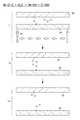
まず、図1及び図2を用いて、H2Oが、金属酸化物層20と樹脂層23との密着性を阻害する作用(以下、阻害作用)について説明する。
First, with reference to FIGS. 1 and 2,
図1において、作製基板14上に金属酸化物層20が設けられ、金属酸化物層20上に樹脂層23が設けられている。
In FIG. 1, a
金属酸化物層20と樹脂層23との界面、及び、金属酸化物層20中のうち一方または双方には、H2O、水素(H)、酸素(O)、水酸基(OH)、水素ラジカル(H*)、酸素ラジカル(O*)、ヒドロキシラジカル(OH*)のうち一つまたは複数が存在する。これらは、金属酸化物層20の成膜工程、金属酸化物層20成膜後の添加(dope)工程等によって供給することができる。図1のステップ(i)では、金属酸化物層20と樹脂層23との界面、及び、金属酸化物層20中に、それぞれ、H2O、H、O等を有する例を示す。
H 2 O, hydrogen (H), oxygen (O), hydroxyl group (OH), hydrogen radicals are present at the interface between the
金属酸化物層20と樹脂層23との界面、及び、金属酸化物層20中に供給されたH、O、H2Oなどは、樹脂層23(例えば、ポリイミド、アクリルなど)を固体化(固化、硬化)させる工程(例えば、350℃での加熱)で当該界面にH2Oとして析出する場合がある。この場合、金属酸化物層20と樹脂層23との界面に析出したH2Oが、金属酸化物層20と、樹脂層23との密着性を阻害する可能性がある。つまり、金属酸化物層20と樹脂層23との界面に析出したH2Oは、密着性を阻害する作用(阻害作用)を有する。図1のステップ(ii)では、金属酸化物層20中のH2Oが金属酸化物層20と樹脂層23との界面に析出する例を示す。また、図1のステップ(ii)では、金属酸化物層20中の水素と水酸基(OH)とが、金属酸化物層20と樹脂層23との界面にH2Oとして析出する例を示す。
The interface between the
次に、作製基板14、金属酸化物層20、及び樹脂層23を有する積層体に光を照射する。図2のステップ(iii)では、作製基板14が上側に位置する状態で積層体を配置する例を示す。図2のステップ(iii)では、搬送機構(図示しない)を用いて、図中の矢印方向に積層体を移動させることで、図の右側から左側に向かって光が照射される。光は、作製基板14を介して、金属酸化物層20と樹脂層23との界面またはその近傍に照射される。ここでは、線状のレーザ光を用いる例を示す。図2のステップ(iii)、(iv)では、線状ビーム26が、作製基板14を介して、加工領域27に照射される例を示す。光照射により、金属酸化物層20と樹脂層23との界面(さらには金属酸化物層20中及び樹脂層23中)が加熱される。また、光照射により、金属酸化物層20と樹脂層23との界面に存在するH2Oが、高エネルギーで瞬間的に気化(蒸発)してアブレーションする(爆発する、ともいう)。
Next, the laminated body having the
図2のステップ(v)では、積層体の上下を反転する例を示す。図2のステップ(vi)では、金属酸化物層20と樹脂層23とが分離されている例を示す。光照射により、H2Oが水蒸気となり、体積が膨張する。これにより、金属酸化物層20と樹脂層23の密着性が弱くなり、金属酸化物層20と樹脂層23の間を分離することができる。
In step (v) of FIG. 2, an example in which the laminated body is turned upside down is shown. In step (vi) of FIG. 2, an example in which the
次に、図3を用いて、金属酸化物層20と樹脂層23との間の結合について説明する。
Next, the bond between the
図3において、金属酸化物層20と樹脂層23とが積層されている。
In FIG. 3, the
金属酸化物層20と樹脂層23との間には、結合が生じていると考えられる。具体的には共有結合、イオン結合、水素結合等の化学結合が、金属酸化物層20と樹脂層23との間に生じている。
It is considered that a bond is formed between the
図3のステップ(i)では、金属酸化物層20が有する金属Mと、樹脂層23が有する炭素Cとが、酸素Oによって結合されている例を示す。
Step (i) of FIG. 3 shows an example in which the metal M contained in the
金属酸化物層20と樹脂層23の積層構造に光を照射する(図3のレーザ光55参照)。ここでは、線状のレーザ光を用いる例を示す。基板と光源とを相対的に移動させることでレーザ光55を走査し、分離したい領域に亘ってレーザ光55を照射する。
Light is applied to the laminated structure of the
光照射により、金属酸化物層20と樹脂層23との界面(さらには金属酸化物層20中及び樹脂層23中)が加熱され、式(1)(下記及び図3参照)の反応が生じる。光を照射することで、H2O(水蒸気)が、金属M−酸素O−炭素Cの結合を切断する。そして、金属酸化物層20と樹脂層23との間の結合を、水素結合にする。
By light irradiation, the interface between the
M−O−C+H2O→M−OH+C−OH・・・(1) M-OC + H 2 O → M-OH + C-OH ... (1)
図3のステップ(ii)では、金属酸化物層20が有する金属Mと酸素Oが結合し、樹脂層23が有する炭素Cと別の酸素Oが結合している例を示す。2つの酸素は、それぞれ、別の水素と共有結合を形成している。また、2つの酸素は、それぞれ、他方の酸素と結合している水素と水素結合を形成している。
In step (ii) of FIG. 3, an example is shown in which the metal M of the
水素結合は、共有結合に比べて極めて弱い結合であるため、容易に切断することができる。また、光照射のエネルギーにより、水は蒸発して水蒸気になる。このとき膨張する力によって、金属酸化物層20と樹脂層23の間の水素結合を切断することができる場合がある。したがって、金属酸化物層20と樹脂層23とを容易に分離することができる。
Since the hydrogen bond is an extremely weak bond as compared with the covalent bond, it can be easily cleaved. In addition, the energy of light irradiation causes water to evaporate into water vapor. At this time, the expanding force may be able to break the hydrogen bond between the
図3のステップ(iii)では、水素結合で結合されていた酸素と水素が離れ、金属酸化物層20と樹脂層23とが分離されている例を示す。金属酸化物層20が有する金属Mと酸素Oが結合し、樹脂層23が有する炭素Cと別の酸素Oが結合している。2つの酸素は、それぞれ、別の水素と共有結合を形成している。
In step (iii) of FIG. 3, an example is shown in which oxygen and hydrogen bonded by hydrogen bonds are separated and the
以上のように、金属酸化物層20と樹脂層23の積層構造に光を照射することで、H2Oが、金属酸化物層20と樹脂層23の間の強固な結合を、弱い結合である水素結合に変える。これにより、金属酸化物層20と樹脂層23の間の分離に要する力を低減させることができる。また、光照射のエネルギーにより、H2Oが膨張することで、金属酸化物層20と樹脂層23とを分離することができる。
As described above, by irradiating light to the multilayer structure of the
次に、上記阻害作用及び上記式(1)に示す反応に係るH2Oについて説明する。 Next, H 2 O will be explained according to the reaction shown in the inhibitory activity and the formula (1).
H2Oは、金属酸化物層20中、樹脂層23中、及び金属酸化物層20と樹脂層23との界面などに存在する場合がある。
H 2 O may be present in the
また、金属酸化物層20中、樹脂層23中、及び金属酸化物層20と樹脂層23との界面などに存在していた水素(H)、酸素(O)、水酸基(OH)、水素ラジカル(H*)、酸素ラジカル(O*)、ヒドロキシラジカル(OH*)等は、加熱されてH2Oとなる場合がある。
Further, hydrogen (H), oxygen (O), hydroxyl group (OH), and hydrogen radicals existing in the
金属酸化物層20の内部、金属酸化物層20の表面(樹脂層23と接する面)、または金属酸化物層20と樹脂層23の界面に、H2O、水素(H)、酸素(O)、水酸基(OH)、水素ラジカル(H*)、酸素ラジカル(O*)、ヒドロキシラジカル(OH*)のうち一つまたは複数を添加することが好ましい。
Internal
なお、本実施の形態の剥離方法では、上記の阻害作用と、先に示す式(1)の反応と、が同時に生じる場合がある。この場合、金属酸化物層20と樹脂層23との密着性をさらに低下させる、別言すると金属酸化物層20と樹脂層23との剥離性をさらに高めることができると推定される。
In the peeling method of the present embodiment, the above-mentioned inhibitory action and the reaction of the above formula (1) may occur at the same time. In this case, it is presumed that the adhesion between the
金属酸化物層20中、樹脂層23中、及び金属酸化物層20と樹脂層23との界面などに、H2O、水素(H)、酸素(O)、水酸基(OH)、水素ラジカル(H*)、酸素ラジカル(O*)、ヒドロキシラジカル(OH*)等を多く有することが好ましい。反応に寄与するH2Oを多くすることで、反応を促進し、分離に要する力をより低減させることができる。
In the
例えば、金属酸化物層20を形成する際に、金属酸化物層20中、または金属酸化物層20表面に、H2O、水素、酸素、水酸基、水素ラジカル(H*)、酸素ラジカル(O*)、ヒドロキシラジカル(OH*)等を多く含ませることが好ましい。
For example, when the metal oxide layer 20 is formed, H 2 O, hydrogen, oxygen, hydroxyl groups, hydrogen radicals (H * ), and oxygen radicals (O) are formed in the
具体的には、金属層を形成し、金属層の表面にラジカル処理を行うことで金属酸化物層20を形成することが好ましい。ラジカル処理では、酸素ラジカル及びヒドロキシラジカルのうち少なくとも一方を含む雰囲気に、金属層の表面を曝すことが好ましい。例えば、酸素または水蒸気(H2O)のうち一方または双方を含む雰囲気でプラズマ処理を行うことが好ましい。
Specifically, it is preferable to form the metal layer and to form the
または、金属酸化物層20を形成し、金属酸化物層20の表面にラジカル処理を行うことが好ましい。ラジカル処理では、酸素ラジカル、水素ラジカル、及びヒドロキシラジカルのうち少なくとも1種を含む雰囲気に、金属酸化物層20の表面を曝すことが好ましい。例えば、酸素、水素、または水蒸気(H2O)のうち一つまたは複数を含む雰囲気でプラズマ処理を行うことが好ましい。
Alternatively, it is preferable to form the
ラジカル処理は、プラズマ発生装置またはオゾン発生装置を用いて行うことができる。 The radical treatment can be performed using a plasma generator or an ozone generator.
例えば、酸素プラズマ処理、水素プラズマ処理、水プラズマ処理、オゾン処理等を行うことができる。酸素プラズマ処理は、酸素を含む雰囲気下でプラズマを生成して行うことができる。水素プラズマ処理は、水素を含む雰囲気下でプラズマを生成して行うことができる。水プラズマ処理は、水蒸気(H2O)を含む雰囲気下でプラズマを生成して行うことができる。特に水プラズマ処理を行うことで、金属酸化物層20の表面または内部に水分を多く含ませることができ好ましい。
For example, oxygen plasma treatment, hydrogen plasma treatment, water plasma treatment, ozone treatment and the like can be performed. The oxygen plasma treatment can be performed by generating plasma in an atmosphere containing oxygen. The hydrogen plasma treatment can be performed by generating plasma in an atmosphere containing hydrogen. Water plasma treatment can be performed by generating a plasma in an atmosphere containing water vapor (
酸素、水素、水(水蒸気)、及び不活性ガス(代表的にはアルゴン)のうち2種以上を含む雰囲気下でのプラズマ処理を行ってもよい。当該プラズマ処理としては、例えば、酸素と水素とを含む雰囲気下でのプラズマ処理、酸素と水とを含む雰囲気下でのプラズマ処理、水とアルゴンとを含む雰囲気下でのプラズマ処理、酸素とアルゴンとを含む雰囲気下でのプラズマ処理、または酸素と水とアルゴンとを含む雰囲気下でのプラズマ処理などが挙げられる。プラズマ処理のガスの一つとして、アルゴンガスを用いることで金属層または金属酸化物層20にダメージを与えながら、プラズマ処理を行うことが可能となるため好適である。
Plasma treatment may be performed in an atmosphere containing two or more of oxygen, hydrogen, water (water vapor), and an inert gas (typically argon). The plasma treatment includes, for example, plasma treatment in an atmosphere containing oxygen and hydrogen, plasma treatment in an atmosphere containing oxygen and water, plasma treatment in an atmosphere containing water and argon, and oxygen and argon. Examples include plasma treatment in an atmosphere containing and, or plasma treatment in an atmosphere containing oxygen, water, and argon. By using argon gas as one of the gases for plasma treatment, it is possible to perform plasma treatment while damaging the metal layer or the
2種以上のプラズマ処理を大気に暴露することなく連続で行ってもよい。例えば、アルゴンプラズマ処理を行った後に、水プラズマ処理を行ってもよい。 Two or more kinds of plasma treatments may be continuously performed without exposure to the atmosphere. For example, water plasma treatment may be performed after argon plasma treatment.
これにより、図4に示すように、金属酸化物層20の表面または内部に、水素、酸素、水素ラジカル(H*)、酸素ラジカル(O*)、ヒドロキシラジカル(OH*)等を含ませることができる。また、図4では、樹脂層23に、炭素Cと結合した水素H、水酸基OHが含まれる例を示す。これらが、加熱処理や光照射により加熱され、H2Oとなることが考えられる。
As a result, as shown in FIG. 4, hydrogen, oxygen, hydrogen radicals (H * ), oxygen radicals (O * ), hydroxyl radicals (OH * ), etc. are contained in the surface or inside of the
ランプ、レーザ装置等を用いて光を照射することができる。 Light can be irradiated using a lamp, a laser device, or the like.
線状レーザ装置を用いてレーザ光を照射することが好ましい。低温ポリシリコン(LTPS(Low Temperature Poly−Silicon))等の製造ラインのレーザ装置を使用することができるため、これらの装置の有効利用が可能である。例えば、LTPSの結晶化工程に用いる線状レーザ装置は、基板の向きを表裏逆にし、作製基板14側を表面としてレーザ光を真上から照射することで、本発明の一態様におけるレーザ光照射工程に、転用可能である。また、既存のLTPSの製造ラインは、酸化物半導体(OS)を用いるトップゲート型のセルフアライン構造のトランジスタの製造ラインに適用できる。このように、既存のLTPSの製造設備は、本発明の一態様の分離工程と、OSトランジスタの製造工程を有する製造設備として容易に切り替え可能である。
It is preferable to irradiate the laser beam using a linear laser device. Since laser devices on a production line such as low-temperature polysilicon (LTPS (Low Temperature Poly-Silicon)) can be used, these devices can be effectively used. For example, in the linear laser apparatus used in the crystallization step of LTPS, the direction of the substrate is reversed and the laser beam is irradiated from directly above with the
線状レーザは、矩形長尺状に集光(線状レーザビームに成形)して、金属酸化物層と樹脂層との界面に光を照射する。 The linear laser collects light in a rectangular elongated shape (formed into a linear laser beam) and irradiates the interface between the metal oxide layer and the resin layer with light.
光は、波長領域が180nm以上450nm以下を有するように照射されることが好ましい。光は、波長領域が308nm又はその近傍を有するように照射されることがより好ましい。 The light is preferably irradiated so that the wavelength region has 180 nm or more and 450 nm or less. It is more preferable that the light is irradiated so that the wavelength region has 308 nm or its vicinity.
本発明の一態様において、作製基板14、金属酸化物層20、及び樹脂層23の積層構造の、レーザ光の吸収率は高いことが好ましい。例えば、当該積層構造における、波長308nmの光の吸収率は、80%以上100%以下であることが好ましく、85%以上100%以下であることが好ましい。レーザ光の大部分が当該積層構造で吸収されることで、分離の歩留まりを高めることができる。また、機能素子にレーザ光が照射されることが抑制され、機能素子の信頼性の低下を抑制できる。
In one aspect of the present invention, it is preferable that the laminated structure of the
光のエネルギー密度は、250mJ/cm2以上400mJ/cm2以下が好ましく、250mJ/cm2以上360mJ/cm2以下がより好ましい。 The energy density of the light is preferably from 250 mJ / cm 2 or more 400 mJ / cm 2 or less, 250 mJ / cm 2 or more 360 mJ / cm 2 or less being more preferred.
レーザ装置を用いて光を照射する場合、同一箇所に照射されるレーザ光のショット数は、1ショット以上50ショット以下とすることができ、1ショットより多く10ショット以下が好ましく、1ショットより多く5ショット以下がより好ましい。 When irradiating light using a laser device, the number of shots of the laser beam radiated to the same location can be 1 shot or more and 50 shots or less, preferably more than 1 shot and 10 shots or less, and more than 1 shot. 5 shots or less is more preferable.
ビームの短軸方向の両端には、光の強度が低い部分が存在する。そのため、当該光の強度が低い部分の幅以上、一つのショットと次のショットの間にオーバーラップする部分を設けることが好ましい。そのため、レーザ光のショット数は、1.1ショット以上とすることが好ましく、1.25ショット以上とすることがより好ましい。 At both ends of the beam in the minor axis direction, there are portions with low light intensity. Therefore, it is preferable to provide an overlapping portion between one shot and the next shot, which is equal to or larger than the width of the portion where the light intensity is low. Therefore, the number of shots of the laser beam is preferably 1.1 shots or more, and more preferably 1.25 shots or more.
なお、本明細書中、レーザ光のショット数とは、ある点(領域)に照射されるレーザ光の照射回数を指し、ビーム幅、スキャン速度、周波数、またはオーバーラップ率などで決定される。また、線状のビームをあるスキャン方向に移動させているパルスとパルスの間、即ち、一つのショットと次のショットの間にオーバーラップする部分があり、その重なる比率がオーバーラップ率である。なお、オーバーラップ率が100%に近ければ近いほどショット数は多く、離れれば離れるほどショット数は少なくなり、スキャン速度が速ければ速いほどショット数は少なくなる。 In the present specification, the number of shots of the laser beam refers to the number of times the laser beam is irradiated to a certain point (region), and is determined by the beam width, the scan speed, the frequency, the overlap rate, and the like. Further, there is an overlapping portion between the pulses moving the linear beam in a certain scanning direction, that is, between one shot and the next shot, and the overlapping ratio is the overlap ratio. The closer the overlap rate is to 100%, the larger the number of shots, the farther away, the smaller the number of shots, and the faster the scanning speed, the smaller the number of shots.
上記のレーザ光のショット数が1.1ショットとは、連続する2つのショットの間にビームの10分の1程度の幅のオーバーラップを有することを示し、オーバーラップ率10%といえる。同様に、1.25ショットとは、連続する2つのショットの間にビームの4分の1程度の幅のオーバーラップを有することを示し、オーバーラップ率25%といえる。 The number of shots of the laser beam of 1.1 shots means that there is an overlap with a width of about 1/10 of the beam between two consecutive shots, and it can be said that the overlap rate is 10%. Similarly, 1.25 shots means that there is an overlap with a width of about a quarter of the beam between two consecutive shots, and it can be said that the overlap rate is 25%.
ここで、LTPSのレーザ結晶化の工程で照射する光のエネルギー密度は高く、例えば350mJ/cm2以上400mJ/cm2以下が挙げられる。また、レーザのショット数も多く必要であり、例えば10ショット以上100ショット以下が挙げられる。 Here, the energy density of the light irradiated in the process of laser crystallization of LTPS is high, and examples thereof include 350 mJ / cm 2 or more and 400 mJ / cm 2 or less. In addition, a large number of laser shots is required, and examples thereof include 10 shots or more and 100 shots or less.
一方、本実施の形態において、金属酸化物層20と樹脂層23とを分離するために行う光の照射は、レーザ結晶化の工程で用いる条件よりも低いエネルギー密度、または少ないショット数で行うことができる。そのため、レーザ装置での処理可能な基板枚数を増やすことができる。また、レーザ装置のメンテナンスの頻度の低減など、レーザ装置のランニングコストの低減が可能となる。したがって、表示装置などの作製コストを低減することができる。
On the other hand, in the present embodiment, the irradiation of light performed to separate the
また、光の照射が、レーザ結晶化の工程で用いる条件よりも低いエネルギー密度、または少ないショット数で行われることから、基板がレーザ光の照射により受けるダメージを低減できる。そのため、基板を一度使用しても、強度が低下しにくく、基板を再利用できる。したがって、コストを抑えることが可能となる。 Further, since the light irradiation is performed with an energy density lower than the conditions used in the laser crystallization step or a small number of shots, the damage to the substrate due to the laser light irradiation can be reduced. Therefore, even if the substrate is used once, the strength does not easily decrease and the substrate can be reused. Therefore, it is possible to reduce the cost.
また、本実施の形態では、作製基板14と樹脂層23との間に金属酸化物層20を配置する。金属酸化物層20を用いることで、金属酸化物層20を用いない場合に比べて、光の照射を、低いエネルギー密度、または少ないショット数で行うことができることがある。
Further, in the present embodiment, the
作製基板を介して光を照射する際、作製基板の光照射面にゴミなどの異物が付着していると、光の照射ムラが生じ、剥離性が低い部分が形成され、金属酸化物層と樹脂層とを分離する工程の歩留まりが低下することがある。そのため、光を照射する前、または光を照射している間に、光照射面を洗浄することが好ましい。例えば、アセトンなどの有機溶剤、水等を用いて作製基板の光照射面を洗浄することができる。また、エアナイフを用いて気体を噴きつけながら光を照射してもよい。これにより、光の照射ムラを低減し、分離の歩留まりを向上させることができる。 When irradiating light through the production substrate, if foreign matter such as dust adheres to the light irradiation surface of the production substrate, uneven light irradiation occurs, a portion having low peelability is formed, and the metal oxide layer and the metal oxide layer are formed. The yield of the process of separating from the resin layer may decrease. Therefore, it is preferable to clean the light-irradiated surface before or during the light irradiation. For example, the light-irradiated surface of the production substrate can be cleaned with an organic solvent such as acetone, water, or the like. Alternatively, light may be irradiated while blowing gas using an air knife. As a result, uneven light irradiation can be reduced and the yield of separation can be improved.
または、本実施の形態では、まず、基板上に金属酸化物層を形成する。次に、金属酸化物層上に樹脂層を形成する。次に、基板上及び樹脂層上に、樹脂層の端部を覆う絶縁層を形成する。次に、樹脂層上に、絶縁層を介して、チャネル形成領域に金属酸化物を有するトランジスタを形成する。次に、金属酸化物層と樹脂層との界面またはその近傍に光を照射する。次に、樹脂層の少なくとも一部を金属酸化物層から分離することで、分離の起点を形成する。そして、金属酸化物層と樹脂層とを分離する。 Alternatively, in the present embodiment, first, a metal oxide layer is formed on the substrate. Next, a resin layer is formed on the metal oxide layer. Next, an insulating layer covering the end of the resin layer is formed on the substrate and the resin layer. Next, a transistor having a metal oxide in the channel forming region is formed on the resin layer via an insulating layer. Next, light is applied to the interface between the metal oxide layer and the resin layer or its vicinity. Next, the starting point of separation is formed by separating at least a part of the resin layer from the metal oxide layer. Then, the metal oxide layer and the resin layer are separated.
基板上には、樹脂層が接する部分と、絶縁層が接する部分と、が設けられる。絶縁層は、樹脂層の端部を覆って設けられる。絶縁層は、樹脂層に比べて、金属酸化物層に対する密着性もしくは接着性が高い。樹脂層の端部を覆って絶縁層を設けることで、光を照射した後に、樹脂層が基板から意図せず剥がれることを抑制できる。例えば、レーザ装置から別の場所に基板を搬送する時などに樹脂層が剥がれることを抑制できる。そして、分離の起点を形成することで、所望のタイミングで、金属酸化物層と樹脂層とを分離することができる。つまり、本実施の形態では、金属酸化物層と樹脂層の分離のタイミングを制御でき、かつ、分離に要する力が小さい。これにより、金属酸化物層と樹脂層の分離工程、及び表示装置の作製工程の歩留まりを高めることができる。 A portion in contact with the resin layer and a portion in contact with the insulating layer are provided on the substrate. The insulating layer is provided so as to cover the end portion of the resin layer. The insulating layer has higher adhesion or adhesiveness to the metal oxide layer than the resin layer. By providing the insulating layer by covering the end portion of the resin layer, it is possible to prevent the resin layer from being unintentionally peeled off from the substrate after being irradiated with light. For example, it is possible to prevent the resin layer from peeling off when the substrate is transported from the laser device to another location. Then, by forming the starting point of separation, the metal oxide layer and the resin layer can be separated at a desired timing. That is, in the present embodiment, the timing of separation of the metal oxide layer and the resin layer can be controlled, and the force required for separation is small. As a result, the yield of the step of separating the metal oxide layer and the resin layer and the step of manufacturing the display device can be increased.
本実施の形態の表示装置は、トランジスタのチャネル形成領域に、金属酸化物を有することが好ましい。金属酸化物は、酸化物半導体として機能することができる。 The display device of the present embodiment preferably has a metal oxide in the channel forming region of the transistor. The metal oxide can function as an oxide semiconductor.
トランジスタのチャネル形成領域に低温ポリシリコン(LTPS(Low Temperature Poly−Silicon))を用いる場合、500℃から550℃程度の温度をかける必要があるため、樹脂層に耐熱性が求められる。また、レーザ結晶化の工程でのダメージを緩和するため、樹脂層の厚膜化が必要となることがある。 When low-temperature polysilicon (LTPS (Low Temperature Poly-Silicon)) is used in the channel formation region of the transistor, it is necessary to apply a temperature of about 500 ° C. to 550 ° C., so that the resin layer is required to have heat resistance. Further, in order to alleviate damage in the process of laser crystallization, it may be necessary to thicken the resin layer.
一方、チャネル形成領域に金属酸化物を用いたトランジスタは、350℃以下、さらには300℃以下で形成することができる。そのため、樹脂層に高い耐熱性は求められない。したがって、樹脂層の耐熱温度を低くすることができ、材料の選択の幅が広がる。 On the other hand, a transistor using a metal oxide in the channel forming region can be formed at 350 ° C. or lower, further 300 ° C. or lower. Therefore, high heat resistance is not required for the resin layer. Therefore, the heat resistant temperature of the resin layer can be lowered, and the range of material selection is widened.
また、チャネル形成領域に金属酸化物を用いたトランジスタは、レーザ結晶化の工程が不要である。そして、本実施の形態では、レーザ結晶化の工程で用いる条件よりも、低いエネルギー密度または少ないショット数で光を照射することができる。また、レーザ結晶化の工程では、レーザ光が基板を介さずに樹脂層に照射されるが、本実施の形態では、作製基板と金属酸化物層とを介して樹脂層に照射される。このように、樹脂層が受けるダメージが少ないため、樹脂層の厚さを薄くすることができる。樹脂層に高耐熱性が要求されず、薄膜化できることで、デバイス作製の大幅なコストダウンが期待できる。また、LTPSを用いる場合に比べて、工程が簡略化でき好ましい。 Further, a transistor using a metal oxide in the channel forming region does not require a laser crystallization step. Then, in the present embodiment, the light can be irradiated with a lower energy density or a smaller number of shots than the conditions used in the laser crystallization step. Further, in the laser crystallization step, the laser beam is irradiated to the resin layer without passing through the substrate, but in the present embodiment, the resin layer is irradiated through the manufactured substrate and the metal oxide layer. As described above, since the resin layer is less damaged, the thickness of the resin layer can be reduced. Since the resin layer is not required to have high heat resistance and can be made into a thin film, a significant cost reduction in device fabrication can be expected. Further, as compared with the case of using LTPS, the process can be simplified, which is preferable.
ただし、本発明の一態様の表示装置は、トランジスタのチャネル形成領域に、金属酸化物を有する構成に限定されない。例えば、本実施の形態の表示装置は、トランジスタのチャネル形成領域に、シリコンを用いることができる。シリコンとしては、アモルファスシリコンまたは結晶性シリコンを用いることができる。結晶性シリコンとしては、微結晶シリコン、多結晶シリコン、単結晶シリコン等が挙げられる。 However, the display device of one aspect of the present invention is not limited to the configuration in which the metal oxide is contained in the channel forming region of the transistor. For example, in the display device of the present embodiment, silicon can be used for the channel formation region of the transistor. As the silicon, amorphous silicon or crystalline silicon can be used. Examples of crystalline silicon include microcrystalline silicon, polycrystalline silicon, and single crystal silicon.
チャネル形成領域には、LTPSを用いることが好ましい。LTPSなどの多結晶シリコンは、単結晶シリコンに比べて低温で形成でき、かつアモルファスシリコンに比べて高い電界効果移動度と高い信頼性を備える。 It is preferable to use LTPS for the channel formation region. Polycrystalline silicon such as LTPS can be formed at a lower temperature than single crystal silicon, and has higher field effect mobility and higher reliability than amorphous silicon.
樹脂層23の厚さは、0.1μm以上5μm以下としてもよい。樹脂層23を薄く形成することで、低コストで表示装置を作製できる。また、表示装置の軽量化及び薄型化が可能となる。また、表示装置の可撓性を高めることができる。
The thickness of the
樹脂層23の可視光の透過性は特に限定されない。例えば、有色の層であってもよく、透明の層であってもよい。ここで、表示装置の表示面側に樹脂層23が位置する場合、樹脂層23が着色している(有色である)と、光取り出し効率が低下する、取り出される光の色味が変わる、表示品位が低下する等の不具合が生じることがある。
The transparency of visible light of the
樹脂層23は、ウエットエッチング装置、ドライエッチング装置、アッシング装置等を用いて除去することができる。特に、酸素プラズマを用いたアッシングを行って樹脂層23を除去することが好適である。
The
本実施の形態では、作製基板14と樹脂層23との間に金属酸化物層20を有する。金属酸化物層20が光を吸収する機能を有するため、樹脂層23の光の吸収率が低くても、光照射による効果が得られる。したがって、可視光の透過率が高い樹脂層23を用いることができる。そのため、表示装置の表示面側に樹脂層23が位置していても、高い表示品位を実現できる。また、表示品位を高めるために、着色している(有色の)樹脂層23を除去する工程を削減できる。また、樹脂層23の材料の選択の幅が広がる。
In the present embodiment, the
樹脂層23の波長450nm以上700nm以下の範囲の光の透過率の平均値は、70%以上100%以下が好ましく、80%以上100%以下が好ましく、90%以上100%以下がより好ましい。
The average value of the light transmittance of the
本実施の形態では、樹脂層の耐熱温度以下の温度で、トランジスタ等を形成する。樹脂層の耐熱性は、例えば、加熱による重量減少率、具体的には5%重量減少温度等で評価できる。本実施の形態の剥離方法及び表示装置の作製方法では、工程中の最高温度を低くすることができる。例えば、本実施の形態では、樹脂層の5%重量減少温度を、200℃以上650℃以下、200℃以上500℃以下、200℃以上400℃以下、または200℃以上350℃以下とすることができる。そのため、材料の選択の幅が広がる。なお、樹脂層の5%重量減少温度は、650℃より高くてもよい。 In the present embodiment, a transistor or the like is formed at a temperature equal to or lower than the heat resistant temperature of the resin layer. The heat resistance of the resin layer can be evaluated, for example, by the weight loss rate due to heating, specifically, the 5% weight loss temperature or the like. In the peeling method and the manufacturing method of the display device of the present embodiment, the maximum temperature during the process can be lowered. For example, in the present embodiment, the 5% weight loss temperature of the resin layer may be set to 200 ° C. or higher and 650 ° C. or lower, 200 ° C. or higher and 500 ° C. or lower, 200 ° C. or higher and 400 ° C. or lower, or 200 ° C. or higher and 350 ° C. or lower. can. Therefore, the range of material selection is widened. The 5% weight loss temperature of the resin layer may be higher than 650 ° C.
分離前または分離中に、分離界面に水を含む液体を供給することが好ましい。分離界面に水が存在することで、樹脂層23と金属酸化物層20との密着性もしくは接着性をより低下させ、分離に要する力を低減させることができる。また、分離界面に水を含む液体を供給することで、樹脂層23と金属酸化物層20との間の結合を弱めるもしくは切断する効果を奏することがある。液体との化学結合を利用して、樹脂層23と金属酸化物層20の間の結合を切って分離を進行させることができる。例えば、樹脂層23と金属酸化物層20との間に水素結合が形成されている場合、水を含む液体が供給されることで、水と、樹脂層23または金属酸化物層20との間に水素結合が形成され、樹脂層23と金属酸化物層20との間の水素結合が切れることが考えられる。
It is preferable to supply a liquid containing water to the separation interface before or during separation. The presence of water at the separation interface can further reduce the adhesion or adhesiveness between the
金属酸化物層20は、表面張力が小さく、水を含む液体に対する濡れ性が高いことが好ましい。これにより、金属酸化物層20の表面全体に水を含む液体を行き渡らせ、分離界面に水を含む液体を容易に供給できる。金属酸化物層20全体に水が広がることで、均一な剥離ができる。
The
金属酸化物層20の水を含む液体との接触角は、0°より大きく60°以下が好ましく、0°より大きく50°以下がより好ましい。なお、水を含む液体に対する濡れ性が極めて高い場合(例えば接触角が約20°以下の場合)には、接触角の正確な値の取得が困難なことがある。金属酸化物層20は、水を含む液体に対する濡れ性が高いほど好適であるため、上記接触角の正確な値が取得できないほど、水を含む液体に対する濡れ性が高くてもよい。
The contact angle of the
分離界面に水を含む液体が存在することで、分離時に生じる静電気が、被剥離層に含まれる機能素子に悪影響を及ぼすこと(半導体素子が静電気により破壊されるなど)を抑制できる。また、イオナイザなどを用いて、分離により露出した被剥離層の表面を除電してもよい。 The presence of a liquid containing water at the separation interface can prevent static electricity generated during separation from adversely affecting the functional elements contained in the layer to be separated (such as the semiconductor element being destroyed by static electricity). Further, the surface of the layer to be peeled exposed by separation may be statically removed by using an ionizer or the like.
分離界面に液体を供給した場合は、分離により露出した被剥離層の表面を乾燥してもよい。 When a liquid is supplied to the separation interface, the surface of the layer to be peeled exposed by separation may be dried.
以下では、本実施の形態の表示装置の作製方法について、具体的に説明する。 Hereinafter, a method for manufacturing the display device according to the present embodiment will be specifically described.
なお、表示装置を構成する薄膜(絶縁膜、半導体膜、導電膜等)は、スパッタリング法、化学気相堆積(CVD:Chemical Vapor Deposition)法、真空蒸着法、パルスレーザ堆積(PLD:Pulsed Laser Deposition)法、原子層成膜(ALD:Atomic Layer Deposition)法等を用いて形成することができる。CVD法としては、プラズマ化学気相堆積(PECVD:Plasma Enhanced Chemical Vapor Deposition)法や、熱CVD法でもよい。熱CVD法の例として、有機金属化学気相堆積(MOCVD:Metal Organic CVD)法を使ってもよい。 The thin films (insulating film, semiconductor film, conductive film, etc.) constituting the display device include a sputtering method, a chemical vapor deposition (CVD) method, a vacuum deposition method, and a pulsed laser deposition (PLD). ) Method, atomic layer deposition (ALD) method, or the like. The CVD method may be a plasma chemical vapor deposition (PECVD) method or a thermal CVD method. As an example of the thermal CVD method, the metalorganic chemical vapor deposition (MOCVD) method may be used.
表示装置を構成する薄膜(絶縁膜、半導体膜、導電膜等)は、スピンコート、ディップ、スプレー塗布、インクジェット、ディスペンス、スクリーン印刷、オフセット印刷、ドクターナイフ、スリットコート、ロールコート、カーテンコート、ナイフコート等の方法により形成することができる。 The thin films (insulating film, semiconductor film, conductive film, etc.) that make up the display device are spin coating, dip, spray coating, inkjet, dispense, screen printing, offset printing, doctor knife, slit coating, roll coating, curtain coating, knife. It can be formed by a method such as coating.
表示装置を構成する薄膜を加工する際には、リソグラフィ法等を用いて加工することができる。または、シャドウマスクを用いた成膜方法により、島状の薄膜を形成してもよい。または、ナノインプリント法、サンドブラスト法、リフトオフ法などにより薄膜を加工してもよい。フォトリソグラフィ法としては、加工したい薄膜上にレジストマスクを形成して、エッチング等により当該薄膜を加工し、レジストマスクを除去する方法と、感光性を有する薄膜を成膜した後に、露光、現像を行って、当該薄膜を所望の形状に加工する方法と、がある。 When processing the thin film constituting the display device, it can be processed by using a lithography method or the like. Alternatively, an island-shaped thin film may be formed by a film forming method using a shadow mask. Alternatively, the thin film may be processed by a nanoimprint method, a sandblast method, a lift-off method, or the like. Photolithography methods include a method of forming a resist mask on a thin film to be processed and processing the thin film by etching or the like to remove the resist mask, and a method of forming a photosensitive thin film and then exposing and developing the film. There is a method of processing the thin film into a desired shape.
リソグラフィ法において光を用いる場合、露光に用いる光は、例えばi線(波長365nm)、g線(波長436nm)、h線(波長405nm)、またはこれらを混合させた光を用いることができる。そのほか、紫外線やKrFレーザ光、またはArFレーザ光等を用いることもできる。また、液浸露光技術により露光を行ってもよい。また、露光に用いる光として、極端紫外光(EUV:Extreme Ultra−violet)やX線を用いてもよい。また、露光に用いる光に換えて、電子ビームを用いることもできる。極端紫外光、X線または電子ビームを用いると、極めて微細な加工が可能となるため好ましい。なお、電子ビームなどのビームを走査することにより露光を行う場合には、フォトマスクは不要である。
When light is used in the lithography method, for example, i-line (
薄膜のエッチングには、ドライエッチング法、ウエットエッチング法、サンドブラスト法などを用いることができる。 A dry etching method, a wet etching method, a sandblasting method, or the like can be used for etching the thin film.
[剥離方法]
まず、作製基板14上に、金属酸化物層20を形成する(図5(A1))。または、作製基板14上に、金属層19と金属酸化物層20とを積層する(図5(A2))。
[Peeling method]
First, the
作製基板14は、搬送が容易となる程度に剛性を有し、かつ作製工程にかかる温度に対して耐熱性を有する。作製基板14に用いることができる材料としては、例えば、ガラス、石英、セラミック、サファイヤ、樹脂、半導体、金属または合金などが挙げられる。ガラスとしては、例えば、無アルカリガラス、バリウムホウケイ酸ガラス、アルミノホウケイ酸ガラス等が挙げられる。
The
上述の通り、本実施の形態では、作製基板14と樹脂層23の間に下地層を形成する。下地層は、樹脂層23との密着性(接着性)が、作製基板14よりも低い層である。本実施の形態では、金属酸化物層20を用いる場合を例に挙げて説明するが、これに限られない。
As described above, in the present embodiment, the base layer is formed between the manufacturing
具体的には、下地層には、チタン、モリブデン、アルミニウム、タングステン、シリコン、インジウム、亜鉛、ガリウム、タンタル、錫、ハフニウム、イットリウム、ジルコニウム、マグネシウム、ランタン、セリウム、ネオジム、ビスマス、及びニオブのうち一つまたは複数を有する層を用いることができる。下地層には、金属、合金、及びそれらの化合物(金属酸化物など)を含むことができる。下地層は、チタン、モリブデン、アルミニウム、タングステン、シリコン、インジウム、亜鉛、ガリウム、タンタル、及び錫のうち一つまたは複数を有することが好ましい。 Specifically, the underlying layer includes titanium, molybdenum, aluminum, tungsten, silicon, indium, zinc, gallium, tantalum, tin, hafnium, yttrium, zirconium, magnesium, lanthanum, cerium, neodymium, bismuth, and niobium. Layers having one or more can be used. The base layer can contain metals, alloys, and compounds thereof (such as metal oxides). The underlayer preferably has one or more of titanium, molybdenum, aluminum, tungsten, silicon, indium, zinc, gallium, tantalum, and tin.
また、下地層の材料は、無機材料に限られず、有機材料を用いてもよい。例えば、有機EL素子のEL層に用いることができる各種有機材料を用いてもよい。下地層として、これら有機材料の蒸着膜を用いることができる。これにより、密着性の低い膜を形成できる。 Further, the material of the base layer is not limited to the inorganic material, and an organic material may be used. For example, various organic materials that can be used for the EL layer of the organic EL element may be used. A vapor-deposited film of these organic materials can be used as the base layer. As a result, a film having low adhesion can be formed.
金属層19には、各種金属や合金等を用いることができる。
Various metals, alloys, and the like can be used for the
金属酸化物層20には、各種金属の酸化物を用いることができる。金属酸化物としては、例えば、酸化チタン(TiOx)、酸化モリブデン、酸化アルミニウム、酸化タングステン、シリコンを含むインジウム錫酸化物(ITSO)、インジウム亜鉛酸化物、In−Ga−Zn酸化物等が挙げられる。
Oxides of various metals can be used for the
そのほか、金属酸化物としては、酸化インジウム、チタンを含むインジウム酸化物、タングステンを含むインジウム酸化物、インジウム錫酸化物(ITO)、チタンを含むITO、タングステンを含むインジウム亜鉛酸化物、酸化亜鉛(ZnO)、ガリウムを含むZnO、酸化ハフニウム、酸化イットリウム、酸化ジルコニウム、酸化ガリウム、酸化タンタル、酸化マグネシウム、酸化ランタン、酸化セリウム、酸化ネオジム、酸化スズ、酸化ビスマス、チタン酸塩、タンタル酸塩、ニオブ酸塩等が挙げられる。 Other metal oxides include indium oxide, indium oxide containing titanium, indium oxide containing tungsten, indium tin oxide (ITO), ITO containing titanium, indium zinc oxide containing tungsten, and zinc oxide (ZnO). ), ZnO containing gallium, hafnium oxide, yttrium oxide, zirconium oxide, gallium oxide, tantalum oxide, magnesium oxide, lanthanum oxide, cerium oxide, neodymium oxide, tin oxide, bismuth oxide, titanate, tantalate, niobic acid Examples include salt.
金属酸化物層20の形成方法に特に限定は無い。例えば、スパッタリング法、プラズマCVD法、蒸着法、ゾルゲル法、電気泳動法、スプレー法等を用いて形成することができる。
The method for forming the
金属層を成膜した後に、当該金属層に酸素を導入することで、金属酸化物層20を形成することができる。このとき、金属層の表面のみ、または金属層全体を酸化させる。前者の場合、金属層に酸素を導入することで、金属層19と金属酸化物層20との積層構造が形成される(図5(A2))。
The
例えば、酸素を含む雰囲気下で金属層を加熱することで、金属層を酸化させることができる。酸素を含むガスを流しながら金属層を加熱することが好ましい。金属層を加熱する温度は、100℃以上500℃以下が好ましく、100℃以上450℃以下がより好ましく、100℃以上400℃以下がより好ましく、100℃以上350℃以下がさらに好ましい。 For example, the metal layer can be oxidized by heating the metal layer in an atmosphere containing oxygen. It is preferable to heat the metal layer while flowing a gas containing oxygen. The temperature for heating the metal layer is preferably 100 ° C. or higher and 500 ° C. or lower, more preferably 100 ° C. or higher and 450 ° C. or lower, more preferably 100 ° C. or higher and 400 ° C. or lower, and further preferably 100 ° C. or higher and 350 ° C. or lower.
金属層は、トランジスタの作製における最高温度以下の温度で加熱されることが好ましい。これにより、表示装置の作製における最高温度が高くなることを防止できる。トランジスタの作製における最高温度以下とすることで、トランジスタの作製工程における製造装置などを流用することが可能となるため、追加の設備投資などを抑制することができる。したがって、生産コストが抑制された表示装置とすることができる。例えば、トランジスタの作製温度が350℃までである場合、加熱処理の温度は350℃以下とすることが好ましい。 The metal layer is preferably heated at a temperature equal to or lower than the maximum temperature in the fabrication of the transistor. This makes it possible to prevent the maximum temperature in the production of the display device from becoming high. By setting the temperature below the maximum temperature in the manufacturing of the transistor, it is possible to divert the manufacturing equipment and the like in the manufacturing process of the transistor, so that additional capital investment and the like can be suppressed. Therefore, the display device can be a display device in which the production cost is suppressed. For example, when the manufacturing temperature of the transistor is up to 350 ° C., the heat treatment temperature is preferably 350 ° C. or lower.
または、金属層の表面にラジカル処理を行うことで金属層を酸化させることができる。ラジカル処理では、酸素ラジカル及びヒドロキシラジカルのうち少なくとも一方を含む雰囲気に、金属層の表面を曝すことが好ましい。例えば、酸素または水蒸気(H2O)のうち一方または双方を含む雰囲気でプラズマ処理を行うことが好ましい。
Alternatively, the metal layer can be oxidized by radically treating the surface of the metal layer. In the radical treatment, it is preferable to expose the surface of the metal layer to an atmosphere containing at least one of oxygen radicals and hydroxyl radicals. For example, it is preferable to perform plasma treatment in an atmosphere containing one or both of the oxygen or water vapor (
上述の通り、金属酸化物層20の表面または内部に、水素、酸素、水素ラジカル(H*)、酸素ラジカル(O*)、ヒドロキシラジカル(OH*)等を含ませることで、金属酸化物層20と樹脂層23との分離に要する力を低減できる。このことからも、金属酸化物層20の形成に、ラジカル処理もしくはプラズマ処理を行うことは好適である。
As described above, the metal oxide layer is formed by including hydrogen, oxygen, hydrogen radicals (H * ), oxygen radicals (O * ), hydroxyl radicals (OH * ), etc. on the surface or inside of the
金属層の表面にラジカル処理もしくはプラズマ処理を行うことで金属層を酸化させる場合、金属層を高温で加熱する工程が不要となる。そのため、表示装置の作製における最高温度が高くなることを防止できる。 When the metal layer is oxidized by radical treatment or plasma treatment on the surface of the metal layer, the step of heating the metal layer at a high temperature becomes unnecessary. Therefore, it is possible to prevent the maximum temperature in manufacturing the display device from becoming high.
または、酸素雰囲気下で、金属酸化物層20を形成することができる。例えば、酸素を含むガスを流しながら、スパッタリング法を用いて金属酸化物膜を成膜することで、金属酸化物層20を形成できる。この場合も、金属酸化物層20の表面にラジカル処理を行うことが好ましい。ラジカル処理では、酸素ラジカル、水素ラジカル、及びヒドロキシラジカルのうち少なくとも1種を含む雰囲気に、金属酸化物層20の表面を曝すことが好ましい。例えば、酸素、水素、または水蒸気(H2O)のうち一つまたは複数を含む雰囲気でプラズマ処理を行うことが好ましい。
Alternatively, the
ラジカル処理の詳細については、先に記した内容を参照できる。 For details of radical treatment, the contents described above can be referred to.
そのほか、酸素、水素、水等の導入方法としては、イオン注入法、イオンドーピング法、プラズマイマージョンイオン注入法等を用いることができる。 In addition, as a method for introducing oxygen, hydrogen, water, etc., an ion implantation method, an ion doping method, a plasma imaging ion implantation method, or the like can be used.
金属層19の厚さは、1nm以上100nm以下が好ましく、1nm以上50nm以下がより好ましく、1nm以上20nm以下がより好ましい。
The thickness of the
金属酸化物層20の厚さは、例えば、1nm以上200nm以下が好ましく、5nm以上100nm以下がより好ましく、5nm以上50nm以下がより好ましい。なお、金属層を用いて金属酸化物層20を形成する場合、最終的に形成される金属酸化物層20の厚さは、成膜した金属層の厚さよりも厚くなることがある。
The thickness of the
分離前または分離中に、金属酸化物層20と樹脂層23との界面に水を含む液体を供給することで、分離に要する力を低減させることができる。金属酸化物層20と当該液体との接触角が小さいほど、液体供給による効果を高めることができる。具体的には、金属酸化物層20の水を含む液体との接触角は、0°より大きく60°以下が好ましく、0°より大きく50°以下がより好ましい。
By supplying a liquid containing water to the interface between the
金属酸化物層20には、酸化チタン、酸化タングステン等が好適である。酸化チタンを用いると、酸化タングステンよりもコストを低減でき、好ましい。
Titanium oxide, tungsten oxide and the like are suitable for the
金属酸化物層20は光触媒機能を有してもよい。光触媒機能を有する金属酸化物層に光を照射することで、光触媒反応を生じさせることができる。これにより、金属酸化物層と樹脂層との結合力を弱め、容易に分離できる場合がある。金属酸化物層20には、金属酸化物層20を活性化させる波長の光を適宜照射することができる。例えば、金属酸化物層20に紫外光を照射する。例えば、金属酸化物層20の成膜後、他の層を介することなく、金属酸化物層20に直接、紫外光を照射してもよい。紫外光の照射には、紫外光ランプを好適に用いることができる。紫外光ランプとしては、水銀ランプ、水銀キセノンランプ、メタルハライドランプ等が挙げられる。または、分離前に行うレーザ照射工程によって、金属酸化物層20を活性化させてもよい。
The
金属もしくは窒素を添加した酸化チタンを用いてもよい。これらの元素を添加した酸化チタンを用いて金属酸化物層20を形成すると、紫外光でなく、可視光によって活性化させることができる。
Titanium oxide to which metal or nitrogen is added may be used. When the
次に、金属酸化物層20上に、第1の層24を形成する(図5(B))。
Next, the
図5(B)では塗布法を用いて金属酸化物層20の一面全体に第1の層24を形成する例を示す。これに限られず、印刷法等を用いて第1の層24を形成してもよい。金属酸化物層20上に、島状の第1の層24、開口または凹凸形状を有する第1の層24等を形成してもよい。
FIG. 5B shows an example in which the
第1の層24は、各種樹脂材料(樹脂前駆体を含む)を用いて形成することができる。
The
第1の層24は、熱硬化性を有する材料を用いて形成することが好ましい。
The
第1の層24は、感光性を有する材料を用いて形成してもよく、感光性を有さない材料(非感光性の材料ともいう)を用いて形成してもよい。
The
感光性を有する材料を用いると、光を用いたリソグラフィ法により、第1の層24の一部を除去し、所望の形状の樹脂層23を形成することができる。
When a photosensitive material is used, a part of the
第1の層24は、ポリイミド樹脂、ポリイミド樹脂前駆体、またはアクリル樹脂を含む材料を用いて形成されることが好ましい。第1の層24は、例えば、ポリイミド樹脂と溶媒を含む材料、ポリアミック酸と溶媒を含む材料、またはアクリル樹脂と溶媒を含む材料等を用いて形成できる。なお、第1の層24として、ポリイミド樹脂またはポリイミド樹脂前駆体を含む材料を用いると、比較的耐熱性を高められるため好適である。一方で、第1の層24として、アクリル樹脂を含む材料を用いると、可視光における透光性を高められるため好適である。ポリイミド樹脂及びアクリル樹脂は、それぞれ、表示装置の平坦化膜等に好適に用いられる材料であるため、成膜装置や材料を共有することができる。そのため本発明の一態様の構成を実現するために新たな装置や材料を必要としない。このように、第1の層24は、特別な材料は必要でなく、表示装置に用いる樹脂材料を用いて形成できるため、コストを削減することができる。
The
具体的には、樹脂層23は、構造式(100)で表される化合物(オキシジフタル酸)の残基を有することが好ましい。
Specifically, the
樹脂層23には、オキシジフタル酸またはオキシジフタル酸誘導体を含む酸成分と、芳香族アミンまたは芳香族アミン誘導体を含むアミン成分と、を用いて得られるポリイミド樹脂が好適である。オキシジフタル酸誘導体としては、例えば、オキシジフタル酸無水物が挙げられる。また、樹脂層23は、フッ素を含んでいてもよい。樹脂層23中にフッ素を含む場合、当該フッ素を用いて、金属酸化物層20と樹脂層23の間の水素結合が形成されることがある。
For the
また、第1の層24に好適に用いることができる、ポリイミド樹脂またはポリイミド樹脂前駆体を含む材料の物性値について、表1に示す。
Table 1 shows the physical property values of the polyimide resin or the material containing the polyimide resin precursor, which can be suitably used for the
表1に示す材料A〜材料Eを用いて樹脂層23を形成することができる。樹脂層23の信頼性を高めることができるため、材料のガラス転移温度(Tg)及び5%重量減少温度は、それぞれ高い方が好ましい。
The
そのほか、第1の層24の形成に用いることができる樹脂材料としては、例えば、エポキシ樹脂、ポリアミド樹脂、ポリイミドアミド樹脂、シロキサン樹脂、ベンゾシクロブテン系樹脂、フェノール樹脂、及びこれら樹脂の前駆体等が挙げられる。
Other resin materials that can be used to form the
第1の層24は、スピンコータを用いて形成することが好ましい。スピンコート法を用いることで、大判基板に薄い膜を均一に形成することができる。
The
第1の層24は、粘度が5cP以上500cP未満、好ましくは5cP以上100cP未満、より好ましくは10cP以上50cP以下の溶液を用いて形成することが好ましい。溶液の粘度が低いほど、塗布が容易となる。また、溶液の粘度が低いほど、気泡の混入を抑制でき、良質な膜を形成できる。
The
そのほか、第1の層24の形成方法としては、ディップ、スプレー塗布、インクジェット、ディスペンス、スクリーン印刷、オフセット印刷、ドクターナイフ、スリットコート、ロールコート、カーテンコート、ナイフコート等が挙げられる。
In addition, as a method for forming the
次に、第1の層24に対して加熱処理を行うことで、樹脂層23を形成する(図5(C))。
Next, the
加熱処理は、例えば、加熱装置のチャンバーの内部に、酸素、窒素、及び希ガス(アルゴンなど)のうち一つまたは複数を含むガスを流しながら行うことができる。または、加熱処理は、大気雰囲気下で加熱装置のチャンバー、ホットプレート等を用いて行うことができる。 The heat treatment can be performed, for example, by flowing a gas containing one or more of oxygen, nitrogen, and a rare gas (argon, etc.) inside the chamber of the heating device. Alternatively, the heat treatment can be performed in an atmospheric atmosphere using a chamber of a heating device, a hot plate, or the like.
大気雰囲気下や酸素を含むガスを流しながら加熱を行うと、樹脂層23が酸化により着色し、可視光に対する透過性が低下することがある。
When heating is performed in an air atmosphere or while flowing a gas containing oxygen, the
そのため、窒素ガスを流しながら、加熱を行うことが好ましい。これにより、加熱雰囲気中に含まれる酸素を大気雰囲気よりも少なくすることができ、樹脂層23の酸化を抑制し、樹脂層23の可視光に対する透過性を高めることができる。
Therefore, it is preferable to heat while flowing nitrogen gas. As a result, the amount of oxygen contained in the heating atmosphere can be reduced as compared with that in the atmospheric atmosphere, the oxidation of the
加熱処理により、樹脂層23中の脱ガス成分(例えば、水素、水等)を低減することができる。特に、樹脂層23上に形成する各層の作製温度以上の温度で加熱することが好ましい。これにより、トランジスタの作製工程における、樹脂層23からの脱ガスを大幅に抑制することができる。
By heat treatment, the degassing component (for example, hydrogen, water, etc.) in the
例えば、トランジスタの作製温度が350℃までである場合、樹脂層23となる膜を350℃以上450℃以下で加熱することが好ましく、400℃以下がより好ましく、375℃以下がさらに好ましい。これにより、トランジスタの作製工程における、樹脂層23からの脱ガスを大幅に抑制することができる。
For example, when the fabrication temperature of the transistor is up to 350 ° C., the film to be the
加熱処理の温度は、トランジスタの作製における最高温度以下の温度とすることが好ましい。トランジスタの作製における最高温度以下とすることで、トランジスタの作製工程における製造装置などを流用することが可能となるため、追加の設備投資などを抑制することができる。したがって、生産コストが抑制された表示装置とすることができる。例えば、トランジスタの作製温度が350℃までである場合、加熱処理の温度は350℃以下とすることが好ましい。 The temperature of the heat treatment is preferably a temperature equal to or lower than the maximum temperature in the fabrication of the transistor. By setting the temperature below the maximum temperature in the manufacturing of the transistor, it is possible to divert the manufacturing equipment and the like in the manufacturing process of the transistor, so that additional capital investment and the like can be suppressed. Therefore, the display device can be a display device in which the production cost is suppressed. For example, when the manufacturing temperature of the transistor is up to 350 ° C., the heat treatment temperature is preferably 350 ° C. or lower.
トランジスタの作製における最高温度と、加熱処理の温度を等しくすると、加熱処理を行うことで表示装置の作製における最高温度が高くなることを防止でき、かつ樹脂層23の脱ガス成分を低減できるため、好ましい。
By making the maximum temperature in the fabrication of the transistor equal to the temperature in the heat treatment, it is possible to prevent the maximum temperature in the fabrication of the display device from becoming high by performing the heat treatment, and it is possible to reduce the degassing component of the
処理時間を長くすることで、加熱温度が比較的低い場合であっても、加熱温度がより高い条件の場合と同等の剥離性を実現できる場合がある。そのため、加熱装置の構成により加熱温度を高められない場合には、処理時間を長くすることが好ましい。 By lengthening the treatment time, even when the heating temperature is relatively low, it may be possible to achieve the same peelability as when the heating temperature is higher. Therefore, when the heating temperature cannot be raised due to the configuration of the heating device, it is preferable to lengthen the treatment time.
加熱処理の時間は、例えば、5分以上24時間以下が好ましく、30分以上12時間以下がより好ましく、1時間以上6時間以下がさらに好ましい。なお、加熱処理の時間はこれに限定されない。例えば、加熱処理を、RTA(Rapid Thermal Annealing)法を用いて行う場合などは、5分未満としてもよい。 The heat treatment time is, for example, preferably 5 minutes or more and 24 hours or less, more preferably 30 minutes or more and 12 hours or less, and further preferably 1 hour or more and 6 hours or less. The heat treatment time is not limited to this. For example, when the heat treatment is performed by using the RTA (Rapid Thermal Annealing) method, it may be less than 5 minutes.
加熱装置としては、電気炉や、抵抗発熱体などの発熱体からの熱伝導または熱輻射によって被処理物を加熱する装置等、様々な装置を用いることができる。例えば、GRTA(Gas Rapid Thermal Anneal)装置、LRTA(Lamp Rapid Thermal Anneal)装置等のRTA装置を用いることができる。LRTA装置は、ハロゲンランプ、メタルハライドランプ、キセノンアークランプ、カーボンアークランプ、高圧ナトリウムランプ、高圧水銀ランプなどのランプから発する光(電磁波)の輻射により、被処理物を加熱する装置である。GRTA装置は、高温のガスを用いて加熱処理を行う装置である。RTA装置を用いることによって、処理時間を短縮することができるので、量産する上で好ましい。また、加熱処理はインライン型の加熱装置を用いて行ってもよい。 As the heating device, various devices such as an electric furnace and a device for heating an object to be processed by heat conduction or heat radiation from a heating element such as a resistance heating element can be used. For example, an RTA device such as a GRTA (Gas Rapid Thermal Anneal) device or an LRTA (Lamp Rapid Thermal Anneal) device can be used. The LRTA device is a device that heats an object to be processed by radiation of light (electromagnetic waves) emitted from lamps such as halogen lamps, metal halide lamps, xenon arc lamps, carbon arc lamps, high-pressure sodium lamps, and high-pressure mercury lamps. The GRTA device is a device that performs heat treatment using a high-temperature gas. By using the RTA device, the processing time can be shortened, which is preferable for mass production. Further, the heat treatment may be performed using an in-line type heating device.
なお、加熱処理により、樹脂層23の厚さは、第1の層24の厚さから変化する場合がある。例えば、第1の層24に含まれていた溶媒が除去されることや、硬化が進行し密度が増大することにより、体積が減少し、第1の層24よりも樹脂層23が薄くなる場合がある。
The thickness of the
加熱処理を行う前に、第1の層24に含まれる溶媒を除去するための熱処理(プリベーク処理ともいう)を行ってもよい。プリベーク処理の温度は用いる材料に応じて適宜決定することができる。例えば、50℃以上180℃以下、80℃以上150℃以下、または90℃以上120℃以下で行うことができる。または、加熱処理がプリベーク処理を兼ねてもよく、加熱処理によって、第1の層24に含まれる溶媒を除去してもよい。
Before the heat treatment, a heat treatment (also referred to as a prebaking treatment) for removing the solvent contained in the
樹脂層23は、可撓性を有する。作製基板14は、樹脂層23よりも可撓性が低い。
The
樹脂層23の厚さは、0.01μm以上10μm未満であることが好ましく、0.1μm以上5μm以下であることがより好ましく、0.5μm以上3μm以下であることがさらに好ましい。樹脂層を薄く形成することで、低コストで表示装置を作製できる。また、表示装置の軽量化及び薄型化が可能となる。また、表示装置の可撓性を高めることができる。低粘度の溶液を用いることで、樹脂層23を薄く形成することが容易となる。ただし、これに限定されず、樹脂層23の厚さは、10μm以上としてもよい。例えば、樹脂層23の厚さを10μm以上200μm以下としてもよい。樹脂層23の厚さを10μm以上とすることで、表示装置の剛性を高めることができるため好適である。
The thickness of the
樹脂層23の熱膨張係数は、0.1ppm/℃以上50ppm/℃以下であることが好ましく、0.1ppm/℃以上20ppm/℃以下であることがより好ましく、0.1ppm/℃以上10ppm/℃以下であることがさらに好ましい。樹脂層23の熱膨張係数が低いほど、加熱により、トランジスタ等を構成する層にクラックが生じることや、トランジスタ等が破損することを抑制できる。
The coefficient of thermal expansion of the
次に、樹脂層23上に、被剥離層25を形成する(図5(D))。
Next, the
被剥離層25として、例えば、絶縁層、機能素子(トランジスタ、表示素子など)を設けることができる。
As the
被剥離層25は、絶縁層を有することが好ましい。当該絶縁層は、後の加熱工程において、金属酸化物層20及び樹脂層23などから放出される水素、酸素、及び水をブロックする機能を有することが好ましい。
The
被剥離層は、例えば、窒化シリコン膜、酸化窒化シリコン膜、または窒化酸化シリコン膜を有することが好ましい。例えば、窒化シリコン膜を、シランガス、水素ガス、及びアンモニア(NH3)ガスを含む成膜ガスを用いたプラズマCVD法により成膜する。絶縁層の厚さは特に限定されない。例えば、50nm以上600nm以下、好ましくは100nm以上300nm以下の厚さとすることができる。 The peeled layer preferably has, for example, a silicon nitride film, a silicon oxide nitride film, or a silicon nitride film. For example, a silicon nitride film is formed by a plasma CVD method using a film-forming gas containing silane gas, hydrogen gas, and ammonia (NH 3) gas. The thickness of the insulating layer is not particularly limited. For example, the thickness can be 50 nm or more and 600 nm or less, preferably 100 nm or more and 300 nm or less.
なお、本明細書等において「酸化窒化シリコン」とは、その組成として、窒素よりも酸素の含有量が多いものをいう。また、本明細書等において、「窒化酸化シリコン」とは、その組成として、酸素よりも窒素の含有量が多いものをいう。 In the present specification and the like, the term "silicon oxide nitride" refers to a composition having a higher oxygen content than nitrogen. Further, in the present specification and the like, "silicon nitride oxide" refers to a composition having a higher nitrogen content than oxygen.
そして、被剥離層25上に保護層を形成する。保護層は、表示装置の最表面に位置する層である。保護層は、可視光に対する透過性が高いことが好ましい。保護層が、有機絶縁膜を有すると、表示装置の表面に傷がつくことや、クラックが生じてしまうことを抑制できるため好ましい。 Then, a protective layer is formed on the layer to be peeled 25. The protective layer is a layer located on the outermost surface of the display device. The protective layer preferably has high transparency to visible light. When the protective layer has an organic insulating film, it is preferable because it is possible to prevent scratches and cracks on the surface of the display device.
図5(D)には、接着層75bを用いて被剥離層25上に基板75aを貼り合わせた例を示す。
FIG. 5D shows an example in which the
接着層75bには、紫外線硬化型等の光硬化型接着剤、反応硬化型接着剤、熱硬化型接着剤、嫌気型接着剤等の各種硬化型接着剤を用いることができる。また、接着シート等を用いてもよい。
For the
基板75aには、例えば、ポリエチレンテレフタレート(PET)、ポリエチレンナフタレート(PEN)等のポリエステル樹脂、ポリアクリロニトリル樹脂、アクリル樹脂、ポリイミド樹脂、ポリメチルメタクリレート樹脂、ポリカーボネート(PC)樹脂、ポリエーテルスルホン(PES)樹脂、ポリアミド樹脂(ナイロン、アラミド等)、ポリシロキサン樹脂、シクロオレフィン樹脂、ポリスチレン樹脂、ポリアミドイミド樹脂、ポリウレタン樹脂、ポリ塩化ビニル樹脂、ポリ塩化ビニリデン樹脂、ポリプロピレン樹脂、ポリテトラフルオロエチレン(PTFE)樹脂、ABS樹脂、セルロースナノファイバー等を用いることができる。基板75aには、可撓性を有する程度の厚さのガラス、石英、樹脂、金属、合金、半導体等の各種材料を用いてもよい。
On the
次に、レーザ光55を照射する(図6(A))。レーザ光55は、例えば、図6(A)においては、左側から右側に走査される線状レーザビームで、その長軸は、その走査方向及びその入射方向(上から下)に垂直である。レーザ装置において、作製基板14が上側にくるように積層体を配置する。積層体には、積層体(作製基板14)の上側からレーザ光55が照射される。
Next, the
レーザ光55は、作製基板14を介して金属酸化物層20と樹脂層23との界面またはその近傍に照射されることが好ましい(図6(A)の加工領域640参照)。また、レーザ光55は、金属酸化物層20中に照射されてもよく、樹脂層23中に照射されてもよい。
The
金属酸化物層20は、レーザ光55を吸収する。樹脂層23は、レーザ光55を吸収してもよい。
The
作製基板14と金属酸化物層20の積層構造におけるレーザ光55の吸収率は、50%以上100%以下が好ましく、75%以上100%以下がより好ましく、80%以上100%以下がさらに好ましい。当該積層構造が、レーザ光55の大半を吸収することで、金属酸化物層と樹脂層23との界面で確実に分離することが可能となる。また、樹脂層23が光から受けるダメージを低減できる。
The absorption rate of the
レーザ光55の照射により、金属酸化物層20と樹脂層23の密着性もしくは接着性が低下する。レーザ光55の照射により、樹脂層23が脆弱化されることがある。
Irradiation with the
レーザ光55としては、少なくともその一部が作製基板14を透過し、かつ金属酸化物層20に吸収される波長の光を選択して用いる。レーザ光55は、可視光線から紫外線の波長領域の光であることが好ましい。例えば波長が180nm以上450nm以下の光、好ましくは200nm以上400nm以下の光、より好ましくは波長が250nm以上350nm以下の光を用いることができる。
As the
レーザ光55は、金属酸化物層20のエネルギーギャップよりも高いエネルギーを有することが好ましい。例えば、酸化チタンのエネルギーギャップは、約3.2eVである。したがって、金属酸化物層20に酸化チタンを用いる場合、光は、3.2eVより高いエネルギーを有することが好ましい。
The
特に、波長308nmのエキシマレーザを用いると、生産性に優れるため好ましい。エキシマレーザは、LTPSにおけるレーザ結晶化にも用いるため、既存のLTPS製造ラインの装置を流用することができ、新たな設備投資を必要としないため好ましい。波長308nmの光のエネルギーは、約4.0eVである。つまり、金属酸化物層20に酸化チタンを用いる場合、波長308nmのエキシマレーザは好適である。また、Nd:YAGレーザの第三高調波である波長355nmのUVレーザなどの固体UVレーザ(半導体UVレーザともいう)を用いてもよい。固体レーザはガスを用いないため、エキシマレーザに比べて、ランニングコストを低減でき、好ましい。また、ピコ秒レーザ等のパルスレーザを用いてもよい。
In particular, it is preferable to use an excimer laser having a wavelength of 308 nm because it is excellent in productivity. Since the excimer laser is also used for laser crystallization in LTPS, the equipment of the existing LTPS production line can be diverted, and new capital investment is not required, which is preferable. The energy of light with a wavelength of 308 nm is about 4.0 eV. That is, when titanium oxide is used for the
レーザ光55として、線状のレーザ光を用いる場合には、作製基板14と光源とを相対的に移動させることでレーザ光55を走査し、分離したい領域に亘ってレーザ光55を照射する。
When a linear laser beam is used as the
ここで、作製基板14の光照射面にゴミなどの異物18が付着していると、光の照射ムラが生じることがある。図7(A)では、作製基板14上に接して樹脂層23が形成されている比較例である。図7(A)では、作製基板14と樹脂層23の界面またはその近傍において、異物18の真下に、光の照射された領域16が途切れている部分を有する。この部分は、他の部分に比べて剥離性が低く、作製基板14と樹脂層23とを分離する工程の歩留まりが低下することが懸念される。
Here, if
一方、本実施の形態では、作製基板14と樹脂層23との間に下地層を形成する。下地層としては、金属層19、金属酸化物層20、または、図7(B)に示すように、金属層19と金属酸化物層20の積層等が挙げられる。下地層は熱伝導性が高い層を有することが好ましい。例えば、図7(B)に示す金属層19の熱伝導性が高いと、作製基板14の光照射面に異物18が付着していても、異物18の周辺の金属層19が加熱されることで、金属層19全体にムラなく熱が伝導する。金属層19の異物18の陰になる部分にも熱が伝わることで、剥離性の低い部分が生じることを抑制できる。図7(B)に示すように、金属層19と金属酸化物層20の界面またはその近傍において、異物18の真下を含んで一面全体に、加熱された領域17が形成される。
On the other hand, in the present embodiment, a base layer is formed between the manufacturing
金属酸化物層20と樹脂層23の界面またはその近傍において、光が当たらない領域は、一箇所または複数箇所設けられていてもよい。光が当たらない領域の面積は、特に限定は無く、例えば、それぞれ、1μm2以上1cm2以下である。場合によっては、光が当たらない領域の面積は、1μm2以下、または1cm2以上であってもよい。
At the interface between the
次に、作製基板14と樹脂層23とを分離する。金属酸化物層20と樹脂層23との密着性もしくは接着性が低いため、金属酸化物層20と樹脂層23との界面で分離が生じる(図6(B1))。また、脆弱化された樹脂層23中で分離が生じる場合もある。
Next, the
例えば、樹脂層23に垂直方向に引っ張る力をかけることにより、作製基板14と樹脂層23とを分離することができる。具体的には、基板75aの上面の一部を吸着し、上方に引っ張ることにより、作製基板14から樹脂層23を引き剥がすことができる。
For example, the
ここで、分離時に、分離界面に水や水溶液など、水を含む液体を添加し、該液体が分離界面に浸透するように分離を行うことで、分離を容易に行うことができる。また、分離時に生じる静電気が、トランジスタなどの機能素子に悪影響を及ぼすこと(半導体素子が静電気により破壊されるなど)を抑制できる。図6(B2)では、液体供給機構21を用いて、分離界面に液体を供給する例を示す。
Here, at the time of separation, a liquid containing water such as water or an aqueous solution is added to the separation interface, and the separation is performed so that the liquid permeates the separation interface, whereby the separation can be easily performed. Further, it is possible to suppress that the static electricity generated at the time of separation adversely affects the functional element such as a transistor (such as the semiconductor element being destroyed by the static electricity). FIG. 6 (B2) shows an example of supplying a liquid to the separation interface by using the
供給する液体としては、水(好ましくは純水)、中性、アルカリ性、もしくは酸性の水溶液や、塩が溶けている水溶液が挙げられる。また、エタノール、アセトン等が挙げられる。また、各種有機溶剤を用いてもよい。 Examples of the liquid to be supplied include water (preferably pure water), a neutral, alkaline or acidic aqueous solution, and an aqueous solution in which a salt is dissolved. Further, ethanol, acetone and the like can be mentioned. Moreover, various organic solvents may be used.
分離前に、樹脂層23の一部を作製基板14から分離することで、分離の起点を形成してもよい。例えば、作製基板14と樹脂層23との間に、刃物などの鋭利な形状の器具を差し込むことで分離の起点を形成してもよい。または、基板75a側から鋭利な形状の器具で樹脂層23を切り込み、分離の起点を形成してもよい。または、レーザアブレーション法等のレーザを用いた方法で、分離の起点を形成してもよい。
Before the separation, a part of the
本実施の形態では、金属酸化物層20及び樹脂層23を積層し、光を照射する。これにより、金属酸化物層20と樹脂層23との密着性もしくは接着性を低下させることができる。そのため、作製基板14と樹脂層23とを容易に分離することができる。
In the present embodiment, the
本実施の形態の剥離方法を用いることで、低コストで量産性の高い剥離方法、または半導体装置の作製方法を提供することができる。例えば、本実施の形態の剥離方法では、作製基板14(例えば、ガラス基板)、または作製基板14と金属酸化物層20との積層体を、複数回繰り返し使うことが可能となるため、生産コストを抑制することができる。
By using the peeling method of the present embodiment, it is possible to provide a peeling method having high mass productivity at low cost or a method for manufacturing a semiconductor device. For example, in the peeling method of the present embodiment, the production substrate 14 (for example, a glass substrate) or the laminate of the
[作製方法例1]
次に、本実施の形態の表示装置の作製方法例について説明する。先に説明した剥離方法と同様の部分について、説明を省略することがある。
[Manufacturing method example 1]
Next, an example of a method for manufacturing the display device of the present embodiment will be described. The description may be omitted for the same part as the peeling method described above.
まず、作製基板14上に、金属酸化物層20を形成する(図8(A))。金属酸化物層20については、上記剥離方法における記載を参照できる。
First, the
次に、金属酸化物層20上に、第1の層24を形成する(図8(B))。第1の層24については、上記剥離方法における記載を参照できる。
Next, the
本実施の形態では、感光性及び熱硬化性を有する材料を用いて第1の層24を形成する。なお、第1の層24は、非感光性の材料を用いて形成してもよい。
In this embodiment, the
第1の層24を成膜した後、溶媒を除去するための熱処理(プリベーク処理)を行い、その後フォトマスクを用いて露光を行う。続いて、現像処理を施すことで、不要な部分を除去することができる。次に、所望の形状に加工された第1の層24に対して加熱処理を行うことで、樹脂層23を形成する(図8(C))。図8(C)では、島状の樹脂層23を形成する例を示す。
After the
なお、樹脂層23の形状は1つの島状に限られず、例えば、複数の島状、開口を有する形状などでもよい。また、ハーフトーンマスクもしくはグレートーンマスクを用いた露光技術、または多重露光技術などを用い、樹脂層23の表面に凹凸形状を形成してもよい。
The shape of the
第1の層24または樹脂層23上にレジストマスク、ハードマスク等のマスクを形成し、エッチングすることで、所望の形状の樹脂層23を形成することができる。この方法は、非感光性の材料を用いる場合に特に好適である。
A
例えば、樹脂層23上に無機膜を形成し、無機膜上にレジストマスクを形成する。レジストマスクを用いて、無機膜をエッチングした後、無機膜をハードマスクに用いて、樹脂層23をエッチングすることができる。
For example, an inorganic film is formed on the
ハードマスクとして用いることができる無機膜としては、各種無機絶縁膜や、導電層に用いることができる金属膜及び合金膜などが挙げられる。 Examples of the inorganic film that can be used as a hard mask include various inorganic insulating films, metal films and alloy films that can be used for the conductive layer.
マスクを極めて薄い厚さで形成し、エッチングと同時にマスクを除去することができると、マスクを除去する工程を削減でき、好ましい。 It is preferable that the mask is formed to have an extremely thin thickness and the mask can be removed at the same time as etching because the step of removing the mask can be reduced.
加熱処理の詳細は、上記剥離方法における加熱処理の記載を参照できる。 For details of the heat treatment, refer to the description of the heat treatment in the above peeling method.
次に、樹脂層23上に、絶縁層31を形成する(図8(D))。絶縁層31は、樹脂層23の端部を覆って形成される。金属酸化物層20上には、樹脂層23が設けられていない部分が存在する。そのため、金属酸化物層20上に接して絶縁層31を形成することができる。
Next, the insulating
絶縁層31は、樹脂層23の耐熱温度以下の温度で形成する。加熱処理の温度より低い温度で形成することが好ましい。
The insulating
絶縁層31は、樹脂層23に含まれる不純物が、後に形成するトランジスタや表示素子に拡散することを防ぐバリア層として用いることができる。例えば、絶縁層31は、樹脂層23を加熱した際に、樹脂層23に含まれる水分等がトランジスタや表示素子に拡散することを防ぐことが好ましい。そのため、絶縁層31は、バリア性が高いことが好ましい。
The insulating
絶縁層31としては、例えば、窒化シリコン膜、酸化窒化シリコン膜、酸化シリコン膜、窒化酸化シリコン膜、酸化アルミニウム膜、窒化アルミニウム膜などの無機絶縁膜を用いることができる。また、酸化ハフニウム膜、酸化イットリウム膜、酸化ジルコニウム膜、酸化ガリウム膜、酸化タンタル膜、酸化マグネシウム膜、酸化ランタン膜、酸化セリウム膜、及び酸化ネオジム膜等を用いてもよい。また、上述の絶縁膜を2以上積層して用いてもよい。特に、樹脂層23上に窒化シリコン膜を形成し、窒化シリコン膜上に酸化シリコン膜を形成することが好ましい。
As the insulating
無機絶縁膜は、成膜温度が高いほど緻密でバリア性の高い膜となるため、高温で形成することが好ましい。 The higher the film formation temperature, the denser the inorganic insulating film and the higher the barrier property, so it is preferable to form the inorganic insulating film at a high temperature.
絶縁層31の成膜時の基板温度は、室温(25℃)以上350℃以下が好ましく、100℃以上300℃以下がさらに好ましい。
The substrate temperature at the time of film formation of the insulating
次に、絶縁層31上に、トランジスタ40を形成する(図8(E))。
Next, the
表示装置が有するトランジスタの構造は特に限定されない。例えば、プレーナ型のトランジスタとしてもよいし、スタガ型のトランジスタとしてもよいし、逆スタガ型のトランジスタとしてもよい。また、トップゲート構造またはボトムゲート構造のいずれのトランジスタ構造としてもよい。または、チャネルの上下にゲート電極が設けられていてもよい。 The structure of the transistor included in the display device is not particularly limited. For example, it may be a planar type transistor, a stagger type transistor, or an inverted stagger type transistor. Further, a transistor structure having either a top gate structure or a bottom gate structure may be used. Alternatively, gate electrodes may be provided above and below the channel.
ここではトランジスタ40として、金属酸化物層44を有する、ボトムゲート構造のトランジスタを作製する場合を示す。金属酸化物層44は、トランジスタ40の半導体層として機能することができる。金属酸化物は、酸化物半導体として機能することができる。
Here, as the
本実施の形態において、トランジスタの半導体には、酸化物半導体を用いる。シリコンよりもバンドギャップが広く、且つキャリア密度の小さい半導体材料を用いると、トランジスタのオフ状態における電流を低減できるため好ましい。 In the present embodiment, an oxide semiconductor is used as the semiconductor of the transistor. It is preferable to use a semiconductor material having a wider bandgap and a smaller carrier density than silicon because the current in the off state of the transistor can be reduced.
トランジスタ40は、樹脂層23の耐熱温度以下の温度で形成する。トランジスタ40は、加熱処理の温度より低い温度で形成することが好ましい。
The
具体的には、まず、絶縁層31上に導電層41を形成する。導電層41は、導電膜を成膜した後、レジストマスクを形成し、当該導電膜をエッチングした後にレジストマスクを除去することで形成できる。
Specifically, first, the
導電膜の成膜時の基板温度は、室温以上350℃以下が好ましく、室温以上300℃以下がさらに好ましい。 The substrate temperature at the time of forming the conductive film is preferably room temperature or higher and 350 ° C. or lower, and more preferably room temperature or higher and 300 ° C. or lower.
表示装置が有する導電層には、それぞれ、アルミニウム、チタン、クロム、ニッケル、銅、イットリウム、ジルコニウム、モリブデン、銀、タンタル、もしくはタングステン等の金属、またはこれを主成分とする合金を単層構造または積層構造として用いることができる。または、酸化インジウム、インジウム錫酸化物(ITO)、タングステンを含むインジウム酸化物、タングステンを含むインジウム亜鉛酸化物、チタンを含むインジウム酸化物、チタンを含むITO、インジウム亜鉛酸化物、酸化亜鉛(ZnO)、ガリウムを含むZnO、またはシリコンを含むITO等の透光性を有する導電性材料を用いてもよい。また、不純物元素を含有させる等して低抵抗化させた、多結晶シリコンもしくは酸化物半導体等の半導体、またはニッケルシリサイド等のシリサイドを用いてもよい。また、グラフェンを含む膜を用いることもできる。グラフェンを含む膜は、例えば酸化グラフェンを含む膜を還元して形成することができる。また、不純物元素を含有させた酸化物半導体等の半導体を用いてもよい。または、銀、カーボン、もしくは銅等の導電性ペースト、またはポリチオフェン等の導電性ポリマーを用いて形成してもよい。導電性ペーストは、安価であり、好ましい。導電性ポリマーは、塗布しやすく、好ましい。 The conductive layer of the display device has a single-layer structure or a metal such as aluminum, titanium, chromium, nickel, copper, yttrium, zirconium, molybdenum, silver, tantalum, or tungsten, or an alloy containing this as a main component. It can be used as a laminated structure. Alternatively, indium oxide, indium tin oxide (ITO), indium oxide containing tungsten, indium zinc oxide containing tungsten, indium oxide containing titanium, ITO containing titanium, indium zinc oxide, zinc oxide (ZnO). , ZnO containing gallium, ITO containing silicon, and other conductive materials having translucency may be used. Further, a semiconductor such as polycrystalline silicon or an oxide semiconductor, which has been reduced in resistance by containing an impurity element or the like, or a silicide such as nickel silicide may be used. A membrane containing graphene can also be used. The graphene-containing film can be formed by reducing, for example, a graphene oxide-containing film. Further, a semiconductor such as an oxide semiconductor containing an impurity element may be used. Alternatively, it may be formed by using a conductive paste such as silver, carbon or copper, or a conductive polymer such as polythiophene. Conductive pastes are inexpensive and preferred. Conductive polymers are preferred because they are easy to apply.
続いて、絶縁層32を形成する。絶縁層32は、絶縁層31に用いることのできる無機絶縁膜を援用できる。
Subsequently, the insulating
続いて、金属酸化物層44を形成する。金属酸化物層44は、金属酸化物膜を成膜した後、レジストマスクを形成し、当該金属酸化物膜をエッチングした後にレジストマスクを除去することで形成できる。
Subsequently, the
金属酸化物膜の成膜時の基板温度は、350℃以下が好ましく、室温以上200℃以下がより好ましく、室温以上130℃以下がさらに好ましい。 The substrate temperature at the time of forming the metal oxide film is preferably 350 ° C. or lower, more preferably room temperature or higher and 200 ° C. or lower, and further preferably room temperature or higher and 130 ° C. or lower.
金属酸化物膜は、不活性ガス及び酸素ガスのいずれか一方または双方を用いて成膜することができる。なお、金属酸化物膜の成膜時における酸素の流量比(酸素分圧)に、特に限定はない。ただし、電界効果移動度が高いトランジスタを得る場合においては、金属酸化物膜の成膜時における酸素の流量比(酸素分圧)は、0%以上30%以下が好ましく、5%以上30%以下がより好ましく、7%以上15%以下がさらに好ましい。 The metal oxide film can be formed by using either one or both of the inert gas and the oxygen gas. The oxygen flow rate ratio (oxygen partial pressure) at the time of forming the metal oxide film is not particularly limited. However, in the case of obtaining a transistor having high field effect mobility, the oxygen flow rate ratio (oxygen partial pressure) at the time of film formation of the metal oxide film is preferably 0% or more and 30% or less, and 5% or more and 30% or less. Is more preferable, and 7% or more and 15% or less is further preferable.
金属酸化物膜は、少なくともインジウムまたは亜鉛を含むことが好ましい。特にインジウム及び亜鉛を含むことが好ましい。 The metal oxide film preferably contains at least indium or zinc. In particular, it preferably contains indium and zinc.
金属酸化物は、エネルギーギャップが2eV以上であることが好ましく、2.5eV以上であることがより好ましく、3eV以上であることがさらに好ましい。このように、エネルギーギャップの広い金属酸化物を用いることで、トランジスタのオフ電流を低減することができる。 The metal oxide preferably has an energy gap of 2 eV or more, more preferably 2.5 eV or more, and even more preferably 3 eV or more. As described above, by using the metal oxide having a wide energy gap, the off-current of the transistor can be reduced.
金属酸化物膜は、スパッタリング法により形成することができる。そのほか、PLD法、PECVD法、熱CVD法、ALD法、真空蒸着法などを用いてもよい。 The metal oxide film can be formed by a sputtering method. In addition, a PLD method, a PECVD method, a thermal CVD method, an ALD method, a vacuum deposition method, or the like may be used.
続いて、導電層43a及び導電層43bを形成する。導電層43a及び導電層43bは、導電膜を成膜した後、レジストマスクを形成し、当該導電膜をエッチングした後にレジストマスクを除去することにより形成できる。導電層43a及び導電層43bは、それぞれ、金属酸化物層44と接続される。
Subsequently, the
なお、導電層43a及び導電層43bの加工の際に、レジストマスクに覆われていない金属酸化物層44の一部がエッチングにより薄膜化する場合がある。
When processing the
導電膜の成膜時の基板温度は、室温以上350℃以下が好ましく、室温以上300℃以下がさらに好ましい。 The substrate temperature at the time of forming the conductive film is preferably room temperature or higher and 350 ° C. or lower, and more preferably room temperature or higher and 300 ° C. or lower.
以上のようにして、トランジスタ40を作製できる(図8(E))。トランジスタ40において、導電層41の一部はゲートとして機能し、絶縁層32の一部はゲート絶縁層として機能し、導電層43a及び導電層43bは、それぞれソースまたはドレインのいずれか一方として機能する。
As described above, the
次に、トランジスタ40を覆う絶縁層33を形成する(図9(A))。絶縁層33は、絶縁層31と同様の方法により形成することができる。
Next, the insulating
また、絶縁層33として、酸素を含む雰囲気下で成膜した酸化シリコン膜や酸化窒化シリコン膜等の酸化物絶縁膜を用いることが好ましい。さらに、当該酸化シリコン膜や酸化窒化シリコン膜上に窒化シリコン膜などの酸素を拡散、透過しにくい絶縁膜を積層することが好ましい。酸素を含む雰囲気下で形成した酸化物絶縁膜は、加熱により多くの酸素を放出しやすい絶縁膜とすることができる。このような酸素を放出する酸化物絶縁膜と、酸素を拡散、透過しにくい絶縁膜を積層した状態で、加熱処理を行うことにより、金属酸化物層44に酸素を供給することができる。その結果、金属酸化物層44中の酸素欠損、及び金属酸化物層44と絶縁層33の界面の欠陥を修復し、欠陥準位を低減することができる。これにより、極めて信頼性の高い表示装置を実現できる。
Further, as the insulating
以上の工程により、樹脂層23上に絶縁層31、トランジスタ40、及び絶縁層33を形成することができる(図9(A))。
By the above steps, the insulating
この段階において、後述する方法を用いて作製基板14とトランジスタ40とを分離することで、表示素子を有さないデバイスを作製することができる。例えば、トランジスタ40や、トランジスタ40に加えて容量素子、抵抗素子、及び配線などを形成することで、半導体装置を作製することができる。
At this stage, a device having no display element can be manufactured by separating the
次に、絶縁層33上に絶縁層34を形成する(図9(A))。絶縁層34は、後に形成する表示素子の被形成面を有する層であるため、平坦化層として機能することが好ましい。絶縁層34は、絶縁層31に用いることのできる有機絶縁膜または無機絶縁膜を援用できる。
Next, the insulating
絶縁層34は、樹脂層23の耐熱温度以下の温度で形成する。絶縁層34は、加熱処理の温度より低い温度で形成することが好ましい。
The insulating
絶縁層34に有機絶縁膜を用いる場合、絶縁層34の形成時に樹脂層23にかかる温度は、室温以上350℃以下が好ましく、室温以上300℃以下がさらに好ましい。
When an organic insulating film is used for the insulating
絶縁層34に無機絶縁膜を用いる場合、成膜時の基板温度は、室温以上350℃以下が好ましく、100℃以上300℃以下がさらに好ましい。
When an inorganic insulating film is used for the insulating
次に、絶縁層34及び絶縁層33に、導電層43bに達する開口を形成する。
Next, an opening reaching the
その後、導電層61を形成する。導電層61は、その一部が発光素子60の画素電極として機能する。導電層61は、導電膜を成膜した後、レジストマスクを形成し、当該導電膜をエッチングした後にレジストマスクを除去することにより形成できる。
After that, the
導電層61は、樹脂層23の耐熱温度以下の温度で形成する。導電層61は、加熱処理の温度より低い温度で形成することが好ましい。
The
導電膜の成膜時の基板温度は、室温以上350℃以下が好ましく、室温以上300℃以下がさらに好ましい。 The substrate temperature at the time of forming the conductive film is preferably room temperature or higher and 350 ° C. or lower, and more preferably room temperature or higher and 300 ° C. or lower.
次に、導電層61の端部を覆う絶縁層35を形成する。絶縁層35は、絶縁層31に用いることのできる有機絶縁膜または無機絶縁膜を援用できる。
Next, the insulating
絶縁層35は、樹脂層23の耐熱温度以下の温度で形成する。絶縁層35は、加熱処理の温度より低い温度で形成することが好ましい。
The insulating
絶縁層35に有機絶縁膜を用いる場合、絶縁層35の形成時に樹脂層23にかかる温度は、室温以上350℃以下が好ましく、室温以上300℃以下がさらに好ましい。
When an organic insulating film is used for the insulating
絶縁層35に無機絶縁膜を用いる場合、成膜時の基板温度は、室温以上350℃以下が好ましく、100℃以上300℃以下がさらに好ましい。
When an inorganic insulating film is used for the insulating
次に、EL層62及び導電層63を形成する。導電層63は、その一部が発光素子60の共通電極として機能する。
Next, the
EL層62は、蒸着法、塗布法、印刷法、吐出法などの方法で形成することができる。EL層62を画素毎に作り分ける場合、メタルマスクなどのシャドウマスクを用いた蒸着法、またはインクジェット法等により形成することができる。EL層62を画素毎に作り分けない場合には、メタルマスクを用いない蒸着法を用いることができる。
The
EL層62には、低分子系化合物及び高分子系化合物のいずれを用いることもでき、無機化合物を含んでいてもよい。
Either a low molecular weight compound or a high molecular weight compound can be used for the
導電層63は、蒸着法やスパッタリング法等を用いて形成することができる。
The
導電層63は、樹脂層23の耐熱温度以下かつEL層62の耐熱温度以下の温度で形成する。また、加熱処理の温度より低い温度で形成することが好ましい。
The
以上のようにして、発光素子60を形成することができる(図9(A))。発光素子60は、一部が画素電極として機能する導電層61、EL層62、及び一部が共通電極として機能する導電層63が積層された構成を有する。
As described above, the
ここでは、発光素子60として、トップエミッション型の発光素子を作製する例を示したが、本発明の一態様はこれに限られない。
Here, an example of producing a top-emission type light-emitting element as the light-emitting
発光素子は、トップエミッション型、ボトムエミッション型、デュアルエミッション型のいずれであってもよい。光を取り出す側の電極には、可視光を透過する導電膜を用いる。また、光を取り出さない側の電極には、可視光を反射する導電膜を用いることが好ましい。 The light emitting element may be any of a top emission type, a bottom emission type, and a dual emission type. A conductive film that transmits visible light is used for the electrode on the side that extracts light. Further, it is preferable to use a conductive film that reflects visible light for the electrode on the side that does not take out light.
次に、導電層63を覆って絶縁層74を形成する(図9(A))。絶縁層74は、発光素子60に水などの不純物が拡散することを抑制する保護層として機能する。発光素子60は、絶縁層74によって封止される。導電層63を形成した後、大気に曝すことなく、絶縁層74を形成することが好ましい。
Next, the insulating
絶縁層74は、樹脂層23の耐熱温度以下かつ発光素子60の耐熱温度以下の温度で形成する。絶縁層74は、加熱処理の温度より低い温度で形成することが好ましい。
The insulating
絶縁層74は、例えば、上述した絶縁層31に用いることのできるバリア性の高い無機絶縁膜が含まれる構成とすることが好ましい。また、無機絶縁膜と有機絶縁膜を積層して用いてもよい。
The insulating
絶縁層74は、ALD法やスパッタリング法等を用いて形成することができる。ALD法及びスパッタリング法は低温成膜が可能であるため好ましい。ALD法を用いると絶縁層74のカバレッジが良好となり好ましい。
The insulating
次に、絶縁層74上に保護層75を形成する(図9(A))。保護層75としては、図5(D)に示すように、接着層75b及び基板75aを用いてもよい。
Next, the
次に、レーザ光55を照射する(図9(B1))。レーザ光55は、例えば、図9(B1)においては、左側から右側に走査される線状レーザビームで、その長軸は、その走査方向及びその入射方向(上から下)に垂直である。レーザ装置において、作製基板14が上側にくるように積層体を配置する。積層体には、積層体(作製基板14)の上側からレーザ光55が照射される。
Next, the
レーザ光の照射工程については、上記剥離方法における記載を参照できる。 For the laser light irradiation step, the description in the above peeling method can be referred to.
なお、1枚の作製基板で複数の表示装置を形成する(多面取りする)場合、1つの樹脂層23を用いて、複数の表示装置を形成することができる。または、複数の樹脂層23を用いて、表示装置ごとに樹脂層23を作り分けてもよい。図9(B2)は作製基板に1つの樹脂層23を有する例である。図9(B3)、(B4)は作製基板に4つの樹脂層23を有する例である。
When a plurality of display devices are formed (multi-chamfered) with one manufacturing substrate, a plurality of display devices can be formed by using one
レーザ装置は、大判の基板の処理が困難であること、もしくは高価であることがある。そのため、作製基板のサイズによっては、図9(B4)に示すように、作製基板を分断した後に、分断した作製基板それぞれに対してレーザ光を照射してもよい。 Laser devices can be difficult or expensive to process large format substrates. Therefore, depending on the size of the production substrate, as shown in FIG. 9 (B4), after the production substrate is divided, each of the divided production substrates may be irradiated with laser light.
次に、樹脂層23に分離の起点を形成する(図10(A)〜(C))。 Next, a starting point for separation is formed in the resin layer 23 (FIGS. 10A to 10C).
例えば、保護層75側から、樹脂層23の端部よりも内側に刃物などの鋭利な形状の器具65を差し込み、枠状に切れ目64を入れる。
For example, from the
または、樹脂層23に、枠状にレーザ光を照射してもよい。
Alternatively, the
上述の通り、多面取りにより、1つの樹脂層23を用いて、複数の表示装置を形成することができる。例えば、図10(B)の切れ目64の内側に、複数の表示装置が配置される。これにより、複数の表示装置を一度にまとめて作製基板と分離することができる。
As described above, by multi-chamfering, one
または、複数の樹脂層23を用いて、表示装置ごとに樹脂層23を作り分けてもよい。図10(C)では、作製基板上に、4つの樹脂層23を形成する例を示す。4つの樹脂層23それぞれに、枠状に切れ目64を入れることで、各表示装置を異なるタイミングで作製基板と分離することができる。
Alternatively, the plurality of resin layers 23 may be used to create
作製方法例1では、金属酸化物層20上に、樹脂層23が接する部分と、絶縁層31が接する部分と、を設ける。金属酸化物層20と絶縁層31との密着性(接着性)は、金属酸化物層20と樹脂層23との密着性(接着性)よりも高い。そのため、樹脂層23が金属酸化物層20から意図せず剥がれることを抑制できる。そして、分離の起点を形成することで、所望のタイミングで、金属酸化物層20と樹脂層23とを分離することができる。したがって、分離のタイミングを制御でき、かつ、分離に要する力が小さい。これにより、分離工程、及び表示装置の作製工程の歩留まりを高めることができる。
In Manufacturing Method Example 1, a portion in contact with the
次に、金属酸化物層20と樹脂層23とを分離する(図11(A))。
Next, the
そして、露出した樹脂層23に、接着層28を用いて、基板29を貼り合わせる(図11(B))。
Then, the
基板29は、表示装置の支持基板として機能することができる。基板29にはフィルムを用いることが好ましく、特に樹脂フィルムを用いることが好ましい。これにより表示装置の軽量化、薄型化が可能となる。また、フィルム基板を用いた表示装置は、ガラスや金属などを用いる場合に比べて、破損しにくい。また、表示装置の可撓性を高めることができる。
The
本実施の形態の剥離方法を用いることで、作製基板14上に作製したトランジスタ40及び発光素子60等を、作製基板14から剥離し、基板29に転置することができる。
By using the peeling method of the present embodiment, the
接着層28には、接着層75bに用いることができる材料を適用することができる。基板29には、基板75aに用いることができる材料を適用することができる。
A material that can be used for the
作製方法例1では、金属酸化物層20及び樹脂層23を積層し、光を照射する。これにより、金属酸化物層20と樹脂層23との密着性もしくは接着性を低下させることができる。そのため、作製基板14と樹脂層23とを容易に分離することができる。
In Production Method Example 1, the
[表示装置の構成例1]
図12(A)は、表示装置10Aの上面図である。図12(B)、(C)は、それぞれ、表示装置10Aの表示部381の断面図及びFPC372との接続部の断面図の一例である。
[Display device configuration example 1]
FIG. 12A is a top view of the display device 10A. 12 (B) and 12 (C) are examples of a cross-sectional view of the
表示装置10Aは、上記の作製方法例1を用いて作製することができる。表示装置10Aは、曲がった状態に保持することや、繰り返し曲げることなどが可能である。
The
表示装置10Aは、保護層75及び基板29を有する。保護層75側が表示装置の表示面側である。表示装置10Aは、表示部381及び駆動回路部382を有する。表示装置10AにはFPC372が貼り付けられている。
The
接続体76を介して、導電層43cとFPC372とが電気的に接続されている(図12(B)、(C))。導電層43cは、トランジスタのソース及びドレインと同一の材料及び同一の工程で形成することができる。
The
接続体76としては、様々な異方性導電フィルム(ACF:Anisotropic Conductive Film)及び異方性導電ペースト(ACP:Anisotropic Conductive Paste)等を用いることができる。
As the
図12(C)に示す表示装置は、トランジスタ40を有さず、トランジスタ49を有している点、及び、絶縁層33上に着色層97を有する点で、図12(B)の構成と異なる。ボトムエミッション型の発光素子60を用いる場合、発光素子60よりも基板29側に着色層97を有していてもよい。上記の作製方法例1では、樹脂層23に可視光の透過率が高い材料を用いることができる。そのため、樹脂層23を介して発光素子60の光を取り出す表示装置であっても、高い表示品位を実現できる。
The display device shown in FIG. 12 (C) has the configuration of FIG. 12 (B) in that it does not have the
図12(C)に示すトランジスタ49は、図12(B)に示すトランジスタ40の構成に加えて、ゲートとして機能する導電層45を有する。
The
トランジスタ49には、チャネルが形成される半導体層を2つのゲートで挟持する構成が適用されている。このような構成とすることで、トランジスタの閾値電圧を制御することができる。2つのゲートを接続し、これらに同一の信号を供給することによりトランジスタを駆動してもよい。このようなトランジスタは他のトランジスタと比較して電界効果移動度を高めることが可能であり、オン電流を増大させることができる。その結果、高速駆動が可能な回路を作製することができる。さらには、回路部の占有面積を縮小することが可能となる。オン電流の大きなトランジスタを適用することで、表示装置を大型化、または高精細化したときに配線数が増大したとしても、各配線における信号遅延を低減することが可能であり、表示ムラを抑制することができる。
A configuration in which a semiconductor layer on which a channel is formed is sandwiched between two gates is applied to the
または、2つのゲートのうち、一方に閾値電圧を制御するための電位を与え、他方に駆動のための電位を与えることで、トランジスタの閾値電圧を制御することができる。 Alternatively, the threshold voltage of the transistor can be controlled by giving a potential for controlling the threshold voltage to one of the two gates and giving a potential for driving to the other.
[作製方法例2]
まず、上記剥離方法と同様に、作製基板14上に、金属酸化物層20から絶縁層31までを形成する(図13(A))。
[Manufacturing method example 2]
First, in the same manner as in the peeling method, the
次に、絶縁層31上にトランジスタ80を形成する(図13(B))。
Next, the
ここではトランジスタ80として、金属酸化物層83と2つのゲートを有するトランジスタを作製する場合を示す。
Here, as the
トランジスタ80は、樹脂層23の耐熱温度以下の温度で形成する。加熱処理の温度より低い温度で形成することが好ましい。
The
具体的には、まず、絶縁層31上に導電層81を形成する。導電層81は、導電膜を成膜した後、レジストマスクを形成し、当該導電膜をエッチングした後にレジストマスクを除去することで形成できる。
Specifically, first, the
続いて、絶縁層82を形成する。絶縁層82は、絶縁層31に用いることのできる無機絶縁膜を援用できる。
Subsequently, the insulating
続いて、金属酸化物層83を形成する。金属酸化物層83は、金属酸化物膜を成膜した後、レジストマスクを形成し、当該金属酸化物膜をエッチングした後にレジストマスクを除去することで形成できる。金属酸化物層83は、金属酸化物層44に用いることのできる材料を援用できる。
Subsequently, the
続いて、絶縁層84及び導電層85を形成する。絶縁層84は、絶縁層31に用いることのできる無機絶縁膜を援用できる。絶縁層84及び導電層85は、絶縁層84となる絶縁膜と、導電層85となる導電膜とを成膜した後、レジストマスクを形成し、当該絶縁膜及び当該導電膜をエッチングした後にレジストマスクを除去することにより形成できる。
Subsequently, the insulating
次に、金属酸化物層83、絶縁層84、及び導電層85を覆う絶縁層33を形成する。絶縁層33は、絶縁層31と同様の方法により形成することができる。
Next, the insulating
絶縁層33は、水素を含むことが好ましい。絶縁層33に含まれる水素が、絶縁層33と接する金属酸化物層83に拡散し、金属酸化物層83の一部が低抵抗化する。金属酸化物層83の一部が低抵抗領域として機能するため、トランジスタ80のオン電流の増大及び電界効果移動度の向上が可能である。
The insulating
次に、絶縁層33に、金属酸化物層83に達する開口を形成する。
Next, an opening is formed in the insulating
続いて、導電層86a及び導電層86bを形成する。導電層86a及び導電層86bは、導電膜を成膜した後、レジストマスクを形成し、当該導電膜をエッチングした後にレジストマスクを除去することにより形成できる。導電層86a及び導電層86bは、それぞれ、絶縁層33の開口を介して金属酸化物層83と電気的に接続される。
Subsequently, the
以上のようにして、トランジスタ80を作製できる(図13(B))。トランジスタ80において、導電層81の一部はゲートとして機能し、絶縁層84の一部はゲート絶縁層として機能し、絶縁層82の一部はゲート絶縁層として機能し、導電層85の一部はゲートとして機能する。金属酸化物層83はチャネル領域と低抵抗領域とを有する。チャネル領域は絶縁層84を介して導電層85と重なる。低抵抗領域は導電層86aと接続される部分と、導電層86bと接続される部分と、を有する。
As described above, the
次に、絶縁層33上に絶縁層34から発光素子60までを形成する(図13(C))。これらの工程は作製方法例1を参照できる。
Next, the insulating
また、図13(A)〜(C)までの工程とは独立して、図14(A)〜(C)の工程を行う。まず、作製基板14上に金属酸化物層20を形成する工程と同様に、作製基板91上に、金属酸化物層92を形成する(図14(A))。次に、金属酸化物層20上に樹脂層23を形成する工程と同様に、金属酸化物層92上に第1の層を形成し、加熱処理を行うことで、樹脂層93を形成する(図14(B))。そして、樹脂層23上に絶縁層31を形成する工程と同様に、樹脂層93上に、樹脂層93の端部を覆う絶縁層95を形成する(図14(B))。
Further, the steps of FIGS. 14 (A) to 14 (C) are performed independently of the steps of FIGS. 13 (A) to 13 (C). First, the
次に、絶縁層95上に、着色層97及び遮光層98を形成する(図14(C))。
Next, a
着色層97として、カラーフィルタ等を用いることができる。着色層97は発光素子60の表示領域と重なるように配置する。
A color filter or the like can be used as the
遮光層98として、ブラックマトリクス等を用いることができる。遮光層98は、絶縁層35と重なるように配置する。
As the light-
次に、作製基板14のトランジスタ80等が形成されている面と、作製基板91の樹脂層93等が形成されている面とを、接着層99を用いて貼り合わせる(図14(D))。
Next, the surface of the
次に、レーザ光55を照射する(図15)。レーザ光55は、例えば、図15においては、左側から右側に走査される線状レーザビームで、その長軸は、その走査方向及びその入射方向(上から下)に垂直である。レーザ装置において、作製基板14が上側にくるように積層体を配置する。積層体には、積層体(作製基板14)の上側からレーザ光55が照射される。
Next, the
作製基板14と作製基板91はどちらを先に分離してもよい。ここでは、作製基板91よりも先に作製基板14を分離する例を示す。
Either the
レーザ光55は、作製基板14を介して金属酸化物層20と樹脂層23との界面またはその近傍に照射されることが好ましい。また、レーザ光55は、金属酸化物層20中に照射されてもよく、樹脂層23中に照射されてもよい。
The
金属酸化物層20は、レーザ光55を吸収する。樹脂層23は、レーザ光55を吸収してもよい。
The
レーザ光55の照射により、金属酸化物層20と樹脂層23の密着性もしくは接着性が低下する。レーザ光55の照射により、樹脂層23が脆弱化されることがある。
Irradiation with the
レーザ光55の大部分は、レーザ光55が照射される側の作製基板、金属酸化物層、及び樹脂層の3層で吸収される。そのため、1度のレーザ光55の照射によって、金属酸化物層20と樹脂層23の密着性または金属酸化物層92と樹脂層93の密着性の一方のみを低下させることができる。作製基板14と作製基板91とで、分離のタイミングを変えることができるため、作製基板14と作製基板91をそれぞれ別工程で分離することができる。これにより、分離工程、及び表示装置の作製工程の歩留まりを高めることができる。
Most of the
レーザ光の照射工程については、上記剥離方法における記載を参照できる。 For the laser light irradiation step, the description in the above peeling method can be referred to.
次に、樹脂層23に分離の起点を形成することが好ましい。例えば、作製基板14と作製基板91の間に鋭利な刃物等を差し込み、作製基板14と作製基板91とが接着層99によって接着されている部分を分離することが好ましい。
Next, it is preferable to form a starting point for separation in the
作製方法例2では、金属酸化物層20上に、樹脂層23が接する部分と、絶縁層31が接する部分と、を設ける。金属酸化物層20と絶縁層31との密着性(接着性)は、金属酸化物層20と樹脂層23との密着性(接着性)よりも高い。そのため、樹脂層23が金属酸化物層20から意図せず剥がれることを抑制できる。同様に、金属酸化物層92上には、樹脂層93が接する部分と、絶縁層95が接する部分と、を設ける。金属酸化物層92と絶縁層95との密着性(接着性)は、金属酸化物層92と樹脂層93との密着性(接着性)よりも高い。そのため、樹脂層93が金属酸化物層92から意図せず剥がれることを抑制できる。
In Manufacturing Method Example 2, a portion in contact with the
次に、作製基板14とトランジスタ80とを分離する(図16(A))。図16(A)では、樹脂層23の端部よりも外側の部分において、接着層99中で分離が生じる(接着層99が凝集破壊する)例を示すが、これに限られない。例えば、接着層99と、絶縁層95または絶縁層33と、の間で分離が生じる(界面破壊または接着破壊が生じるともいう)場合がある。
Next, the
作製方法例2では、金属酸化物層20及び樹脂層23を積層し、光を照射する。これにより、金属酸化物層20と樹脂層23との密着性もしくは接着性を低下させることができる。そのため、作製基板14と樹脂層23とを容易に分離することができる。
In Production Method Example 2, the
次に、作製基板14から分離することで露出した樹脂層23と、基板29とを、接着層28を用いて貼り合わせる(図16(B))。基板29は、表示装置の支持基板として機能することができる。
Next, the
次に、レーザ光55を照射する(図17)。レーザ光55は、例えば、図17においては、左側から右側に走査される線状レーザビームで、その長軸は、その走査方向及びその入射方向(上から下)に垂直である。レーザ装置において、作製基板91が上側にくるように積層体を配置する。積層体には、積層体(作製基板91)の上側からレーザ光55が照射される。
Next, the
レーザ光55は、作製基板91を介して金属酸化物層92と樹脂層93との界面またはその近傍に照射されることが好ましい。また、レーザ光55は、金属酸化物層92中に照射されてもよく、樹脂層93中に照射されてもよい。
The
金属酸化物層92は、レーザ光55を吸収する。樹脂層93は、レーザ光55を吸収してもよい。
The
レーザ光55の照射により、金属酸化物層92と樹脂層93の密着性もしくは接着性が低下する。レーザ光55の照射により、樹脂層93が脆弱化されることがある。
Irradiation with the
レーザ光の照射工程については、上記剥離方法における記載を参照できる。 For the laser light irradiation step, the description in the above peeling method can be referred to.
次に、樹脂層93に分離の起点を形成する(図18(A))。 Next, a starting point for separation is formed in the resin layer 93 (FIG. 18 (A)).
図18(A)では、基板29側から、樹脂層93の端部よりも内側に刃物などの鋭利な形状の器具65を差し込み、枠状に切れ目を入れる。基板29に樹脂を用いる場合に好適である。
In FIG. 18A, a sharp-shaped
または、樹脂層23に分離の起点を形成した際と同様に、作製基板91側から、樹脂層93に、枠状にレーザ光を照射してもよい。
Alternatively, the
分離の起点を形成することで、所望のタイミングで、作製基板91と樹脂層93とを分離することができる。したがって、分離のタイミングを制御でき、かつ、分離に要する力が小さい。これにより、分離工程、及び表示装置の作製工程の歩留まりを高めることができる。
By forming the starting point of separation, the
次に、作製基板91とトランジスタ80とを分離する(図18(B))。ここでは、枠状に切れ目を入れた内側の部分と作製基板91とを分離する例を示す。
Next, the
作製方法例2では、金属酸化物層92及び樹脂層93を積層し、光を照射する。これにより、金属酸化物層92と樹脂層93との密着性もしくは接着性を低下させることができる。そのため、作製基板91と樹脂層93とを容易に分離することができる。
In Production Method Example 2, the
次に、作製基板91から分離することで露出した樹脂層93と、基板22とを、接着層13を用いて貼り合わせる(図19(A))。基板22は、表示装置の支持基板として機能することができる。
Next, the
図19(A)において、発光素子60の発光は、着色層97、絶縁層95、及び樹脂層93を通して、表示装置の外部に取り出される。そのため、樹脂層93の可視光の透過率は高いことが好ましい。本発明の一態様では、樹脂層93の厚さを薄くすることができる。そのため、樹脂層93の可視光の透過率を高め、発光素子60の光取り出し効率の低下を抑制できる。
In FIG. 19A, the light emitted from the
また、本発明の一態様では、金属酸化物層92と樹脂層93との界面またはその近傍に光を照射し、金属酸化物層92が光の一部を吸収する。そのため、樹脂層93の光の吸収率が低くても、金属酸化物層92と樹脂層93とを容易に分離することができる。よって、樹脂層93に可視光の透過率が高い材料を用いることができる。したがって、発光素子60の光取り出し効率の低下を抑制できる。
Further, in one aspect of the present invention, the interface between the
樹脂層93を除去してもよい。これにより、発光素子60の光取り出し効率をさらに高めることができる。図19(B)では、樹脂層93を除去し、接着層13を用いて絶縁層95に基板22を貼り合わせた例を示す。
The
接着層13には、接着層75bに用いることができる材料を適用できる。
A material that can be used for the
基板22には、基板75aに用いることができる材料を適用できる。
A material that can be used for the
作製方法例2は、本発明の一態様の剥離方法を2回行って表示装置を作製する例である。本発明の一態様では、表示装置を構成する機能素子等は、全て作製基板上で形成するため、精細度の高い表示装置を作製する場合においても、可撓性を有する基板には、高い位置合わせ精度が要求されない。よって、簡便に可撓性を有する基板を貼り付けることができる。 Production method example 2 is an example in which a display device is produced by performing the peeling method of one aspect of the present invention twice. In one aspect of the present invention, since all the functional elements and the like constituting the display device are formed on the manufactured substrate, even when the display device having high definition is manufactured, the position is high on the flexible substrate. Alignment accuracy is not required. Therefore, a flexible substrate can be easily attached.
[変形例]
作製方法例2(図14(D))では、接着層99が、金属酸化物層20と絶縁層31とが接している部分、及び金属酸化物層92と絶縁層95とが接している部分の双方と重ねて設けられる場合を示した。
[Modification example]
In Manufacturing Method Example 2 (FIG. 14 (D)), the
金属酸化物層20と絶縁層31の密着性(接着性)、及び金属酸化物層92と絶縁層95の密着性(接着性)は、それぞれ、金属酸化物層20と樹脂層23の密着性(接着性)、及び金属酸化物層92と樹脂層93の密着性(接着性)よりも高い。
The adhesion (adhesiveness) between the
金属酸化物層20と絶縁層31の界面または金属酸化物層92と絶縁層95の界面で剥離を行うと、剥離不良が生じるなど、剥離の歩留まりが低下することがある。そのため、樹脂層に分離の起点を枠状に形成した後、樹脂層と重なる部分のみを作製基板と分離する工程が好適である。
When peeling is performed at the interface between the
一方、図20(A)、(B)に示すように、接着層99を、金属酸化物層20と絶縁層31とが接している部分、及び金属酸化物層92と絶縁層95とが接している部分とは重ねない構成とすることができる。これにより、剥離不良を低減させることができる。
On the other hand, as shown in FIGS. 20A and 20B, the
例えば、流動性の低い接着剤、または接着シートなどを接着層99に用いると、接着層99を島状に形成することが容易である(図20(A))。
For example, when an adhesive having low fluidity, an adhesive sheet, or the like is used for the
または、枠状の隔壁96を形成し、隔壁96に囲まれた内側に接着層99を充填し硬化してもよい(図20(B))。
Alternatively, a frame-shaped
隔壁96を表示装置の構成要素として用いる場合、隔壁96には、硬化した樹脂を用いることが好ましい。このとき、隔壁96も、金属酸化物層20と絶縁層31とが接している部分、及び金属酸化物層92と絶縁層95とが接している部分とは重ねないことが好ましい。
When the
隔壁96を表示装置の構成要素として用いない場合、隔壁96には、未硬化または半硬化の樹脂を用いることが好ましい。このとき、隔壁96を金属酸化物層20と絶縁層31とが接している部分、及び金属酸化物層92と絶縁層95とが接している部分の一方または双方と重ねてもよい。
When the
本実施の形態では、隔壁96に未硬化の樹脂を用い、隔壁96が、金属酸化物層20と絶縁層31とが接している部分、及び金属酸化物層92と絶縁層95とが接している部分と重ならない例を示す。
In the present embodiment, an uncured resin is used for the
[表示装置の構成例2]
図21(A)は、表示装置10Bの上面図である。図21(B)は、表示装置10Bの表示部381の断面図及びFPC372との接続部の断面図の一例である。
[Display device configuration example 2]
FIG. 21A is a top view of the
表示装置10Bは、上記の作製方法例2を用いて作製することができる。表示装置10Bは、曲がった状態に保持することや、繰り返し曲げることなどが可能である。
The
表示装置10Bは、基板22及び基板29を有する。基板22側が表示装置10Bの表示面側である。表示装置10Bは、表示部381及び駆動回路部382を有する。表示装置10BにはFPC372が貼り付けられている。
The
基板22及び基板29にはフィルムを用いることが好ましく、特に樹脂フィルムを用いることが好ましい。これにより表示装置の軽量化、薄型化が可能となる。また、フィルム基板を用いた表示装置は、ガラスや金属などを用いる場合に比べて、破損しにくい。また、表示装置の可撓性を高めることができる。
It is preferable to use a film for the
接続体76を介して、導電層86cとFPC372とが電気的に接続されている(図21(B))。導電層86cは、トランジスタのソース及びドレインと同一の材料及び同一の工程で形成することができる。
The
[積層体の作製装置の例]
次に、図22を用いて、積層体の作製装置の一例を説明する。図22に示す積層体の作製装置は、本実施の形態の剥離方法を用いて作製基板から被剥離層を剥離し、被剥離層を別の基板に転置することができる。図22に示す積層体の作製装置を用いて、半導体装置、表示装置等の積層体を作製することができる。
[Example of a laminated body manufacturing device]
Next, an example of an apparatus for producing a laminated body will be described with reference to FIG. The apparatus for producing a laminated body shown in FIG. 22 can peel the layer to be peeled from the manufactured substrate by using the peeling method of the present embodiment and transfer the layer to be peeled to another substrate. A laminated body such as a semiconductor device and a display device can be manufactured by using the laminated body manufacturing apparatus shown in FIG.
図22に示す積層体の作製装置は、レーザ照射ユニット610、基板反転ユニット630、複数の搬送ローラ(搬送ローラ643、644、645、646等)、テープリール602、巻き取りリール683、方向転換ローラ604、及び押圧ローラ606を有する。
The apparatus for producing the laminated body shown in FIG. 22 includes a
図22に示す積層体の作製装置で処理できる積層体56は、例えば被剥離体56aと支持体56bが積層された構成を有する。積層体56は、被剥離体56aと支持体56bとの間で剥離が生じる。被剥離体56aは例えば樹脂層を有し、支持体56bは例えば作製基板を有する。
The
図22に示す積層体の作製装置は、積層体56に支持体601を貼り付け、支持体601を引っ張ることで被剥離体56aを積層体56から剥離する。支持体601を用いて、積層体56を自動的に分離することができ、作業時間の短縮及び製品の製造歩留まりを向上させることができる。
The apparatus for producing the laminated body shown in FIG. 22 attaches the
支持体56bと分離された被剥離体56aは、接着剤を用いて支持体671と貼り合わされる。これにより、支持体601、被剥離体56a、及び支持体671がこの順で積層された積層体59を作製することができる。
The
複数の搬送ローラは、積層体56を搬送することができる。積層体56を搬送する搬送機構は、搬送ローラに限られず、ベルトコンベア、または搬送ロボット等を用いてもよい。また、搬送機構上のステージに、積層体56を配置してもよい。
The plurality of transport rollers can transport the
搬送ローラ643、搬送ローラ644、搬送ローラ645、搬送ローラ646は、複数に並べられた搬送ローラの1つであり、所定の間隔で設けられ、積層体56、被剥離体56a、または支持体56bの送出方向(実線矢印で示す右回転する方向)に回転駆動される。複数に並べられた搬送ローラは、それぞれ図示しない駆動部(モータ等)により回転駆動される。
The
レーザ照射ユニット610は、積層体56にレーザを照射するユニットである。レーザとしては、例えば波長308nmの紫外光を出力するエキシマレーザなどを用いることができる。また、高圧水銀ランプやUV−LEDなどを用いてもよい。
The
図22に示すように、積層体56は、上側に支持体56bが位置する状態で、レーザ照射ユニット610に搬送される。
As shown in FIG. 22, the
エキシマレーザは高出力のパルスレーザであり、光学系にてビームを線状に整形することができる。線状ビームのレーザ光の照射位置において基板を移動させることで基板全体または必要箇所にレーザ光を照射することができる。なお、線状ビームは、用いる基板の一辺と同等以上の長さとすれば、基板を一方向に移動するのみで基板全体にレーザ光を照射することができる。パルスレーザの発振周波数は、1Hz以上300Hz以下が好ましく、60Hz近傍がより好ましい。 The excimer laser is a high-power pulse laser, and the beam can be linearly shaped by an optical system. By moving the substrate at the irradiation position of the laser beam of the linear beam, the laser beam can be irradiated to the entire substrate or a necessary place. If the linear beam has a length equal to or longer than one side of the substrate to be used, the entire substrate can be irradiated with the laser beam only by moving the substrate in one direction. The oscillation frequency of the pulse laser is preferably 1 Hz or more and 300 Hz or less, and more preferably around 60 Hz.
エキシマレーザ装置には、レーザ発振器を一つ搭載した装置の他、二つ以上のレーザ発振器を搭載する装置を用いることもできる。複数のレーザ発振器を搭載する装置においては、それぞれのレーザ発振器から同期されて出力されたレーザ光を光学系にて合成する(重ね合わす)ことで高エネルギー密度のレーザ光を得ることができる。したがって、本実施の形態の用途においては、第3.5世代(600mm×720mm)以上、第6世代(1500mm×1850mm)以上、第7世代(1870mm×2200mm)以上、または第8世代(2160mm×2460mm)以上のサイズのガラス基板の処理を行うこともできる。また、複数のレーザ発振器を搭載する装置では、それぞれのレーザ発振器から出力されるレーザ光が互いに出力ばらつきを補完するため、1パルス毎の強度ばらつきが少なくなり、歩留りの高い処理を行うことができる。なお、複数の発振器に替えて、複数のエキシマレーザ装置を用いてもよい。 As the excimer laser device, in addition to a device equipped with one laser oscillator, a device equipped with two or more laser oscillators can also be used. In a device equipped with a plurality of laser oscillators, a laser beam having a high energy density can be obtained by synthesizing (superimposing) the laser beams synchronously output from the respective laser oscillators in an optical system. Therefore, in the application of the present embodiment, the third generation (600 mm × 720 mm) or more, the sixth generation (1500 mm × 1850 mm) or more, the seventh generation (1870 mm × 2200 mm) or more, or the eighth generation (2160 mm ×). It is also possible to process a glass substrate having a size of 2460 mm) or more. Further, in a device equipped with a plurality of laser oscillators, the laser light output from each laser oscillator complements each other's output variation, so that the intensity variation for each pulse is reduced and high yield processing can be performed. .. A plurality of excimer laser devices may be used instead of the plurality of oscillators.
図23(A)にエキシマレーザを用いたレーザ照射ユニット610の一例を示す。二つのレーザ発振器を有するエキシマレーザ装置660から出力されたレーザ光610a、610bは光学系635にて合成される。さらに光学系635にて横長に伸張されたレーザ光610cは、ミラー650を介してレンズ680に入射する。レンズ680を透過したレーザ光610dはレーザ光610cに比べて縮小される。このとき、レーザ光610dが、積層体56が有する加工領域640に支持体56b(例えばガラス基板)を介して照射されるようにする。以下では、レーザ光610dのうち、加工領域640に照射される部分を、線状ビーム610eと記す。
FIG. 23 (A) shows an example of the
なお、ここでは二つのレーザ発振器を有する例を示したが、一つのレーザ発振器を有する構成としてもよく、これにより、装置を簡略化できる。また、三つ以上のレーザ発振器を有する構成としてもよく、これにより線状ビーム610eの強度を高めることができる。
Although an example having two laser oscillators is shown here, a configuration having one laser oscillator may be used, whereby the apparatus can be simplified. Further, the configuration may include three or more laser oscillators, whereby the intensity of the
そして、搬送ローラ644により図中の矢印方向に積層体56を移動させることで、加工領域640に線状ビーム610eを照射することができる。
Then, by moving the
図23(A)に示すように、積層体56を搬送ローラ644により一定の速度で搬送しながら線状ビーム610eを照射することにより、プロセス時間を短縮することが可能となる。なお、積層体56を少なくとも一方向に移動可能なステージに配置し、ステージを動かしながら線状ビーム610eを照射してもよい。なお、ステージを用いる場合には、進行方向に対して横方向、及び高さ方向に移動可能なステージを用い、線状ビーム610eの焦点の位置や深さを調整できる構成とすることが好ましい。なお、図23(A)では、積層体56を移動させることで、線状ビーム610eを照射する構成について例示したがこれに限定されない。例えば、積層体56を固定し、エキシマレーザ装置660などを移動させて、積層体56に線状ビーム610eを照射してもよい。
As shown in FIG. 23A, the process time can be shortened by irradiating the
図23(A)では、線状ビーム610eが照射される加工領域640が、積層体56の端部よりも内側に位置する例を示している。これにより、加工領域640の外側の領域は密着性が高い状態を維持するため、搬送時に剥離が生じてしまうことを抑制できる。なお、線状ビーム610eの幅が積層体56の幅と等しい、または積層体56の幅よりも大きくてもよい。その場合、積層体56全体に線状ビーム610eが照射することができる。
FIG. 23A shows an example in which the processed
図23(B)に、線状ビーム610eが積層体56の加工領域640に照射される様子を示す。積層体56は、作製基板58と、第1の層57aと、第2の層57bとを有する。ここで、作製基板58と第2の層57bを含む部分が支持体56bに相当し、第1の層57aを含む部分が被剥離体56aに相当する。
FIG. 23B shows how the
例えば、第1の層57aが上記樹脂層23に相当し、第2の層57bが上記金属酸化物層20に相当する。
For example, the
レーザ光610dは、作製基板58を透過し、線状ビーム610eは、第1の層57aと第2の層57bの界面、またはその近傍に照射されることが好ましい。特に、線状ビーム610eは、第1の層57aと第2の層57bの界面、またはその近傍に焦点が位置することが好ましい。
It is preferable that the
また、第1の層57aと第2の層57bとの界面に線状ビーム610eの焦点が位置することで、第1の層57aと第2の層57bとの界面に存在しうる水が気化し、水の体積が急激に膨張する場合がある。この場合、水の体積の膨張に伴い、第1の層57aと第2の層57bとの界面、またはその近傍で剥離現象が生じると推定される。
Further, since the focal point of the
なお、アモルファスシリコン膜にレーザ光を照射して、アモルファスシリコン膜を結晶化させる技術がある。当該技術の場合、アモルファスシリコン膜の内部にレーザ光の焦点を合わせる。しかしながら、本発明の一態様においては、図23(B)に示すように、レーザ光(ここでは、線状ビーム610e)の焦点は、第1の層57aと、第2の層57bとの界面またはその近傍である。このように本発明の一態様は、レーザ光の焦点位置がアモルファスシリコン膜を結晶化させる技術と相違している。
There is a technique for crystallizing an amorphous silicon film by irradiating the amorphous silicon film with a laser beam. In the case of this technique, the laser beam is focused inside the amorphous silicon film. However, in one aspect of the present invention, as shown in FIG. 23B, the focal point of the laser beam (here, the
また、線状ビーム610eの焦点深度が十分に大きい(深い)場合、第1の層57aと第2の層57bの界面またはその近傍だけでなく、第1の層57aの厚さ方向全体、第2の層57bの厚さ方向全体、または第1の層57aと第2の層57bの両方の厚さ方向全体に亘って、線状ビーム610eの焦点が位置する場合がある。
When the depth of focus of the
なお、エキシマレーザとしては、波長308nmまたはそれよりも波長が長いものを用いることが好ましい。波長308nm以上であれば、支持体56bにガラス基板を用いた場合においても加工に必要なレーザ光を十分に透過させることができる。
As the excimer laser, it is preferable to use a laser having a wavelength of 308 nm or longer. When the wavelength is 308 nm or more, the laser light required for processing can be sufficiently transmitted even when a glass substrate is used for the
図22に示す基板反転ユニット630は、積層体56の上下を入れ替えるユニットである。例えば積層体56の上下を挟む搬送ローラを有し、当該搬送ローラが回転する機構を有する構成とすることができる。なお、基板反転ユニット630の構成はこれに限られず、積層体56の上下を挟む搬送ローラが、らせん状に配置された構成としてもよいし、反転可能な搬送アームを有する構成としてもよい。
The
基板反転ユニット630を通過した積層体56は、図22に示すように、被剥離体56aが上側に位置する状態となる。
As shown in FIG. 22, the
テープリール602は、ロールシート状の支持体601を繰り出すことができる。支持体601を繰り出す速度は可変であることが好ましい。例えば、該速度を比較的遅くすることで、積層体の剥離不良、または剥離した部材におけるクラックの発生を抑制できる。
The
巻き取りリール683は、積層体59を巻き取ることができる。
The take-up
テープリール602及び巻き取りリール683を用いて、支持体601に張力を加えることができる。
Tension can be applied to the
支持体601は、連続的または間欠的に繰り出される。支持体601を連続的に繰り出すと、均一な速度、均一な力で剥離を行うことができるため、好ましい。剥離工程においては、剥離の進行が途中で停止することなく連続することが好ましく、等速で剥離を進行させることがより好ましい。剥離の進行を途中で停止し再び当該領域から剥離を始めると、剥離の進行が連続した場合とは異なり、当該領域に歪等がかかる。そのため、当該領域の微細構造の変化、または当該領域にある電子デバイス等の特性変化が起こり、例えば表示装置などでは、その影響が表示に現れることがある。
The
支持体601として、有機樹脂、金属、合金、またはガラス等を用いたロールシート状のフィルムを用いることができる。
As the
図22では、支持体601に、可撓性基板など、作製する装置(例えばフレキシブルデバイス)を被剥離体56aとともに構成する部材を用いる。支持体601は、キャリアテープなど、作製する装置を構成しない部材であってもよい。
In FIG. 22, a member such as a flexible substrate is used for the
方向転換ローラ604によって、支持体601の送り方向を変えることができる。図22では、方向転換ローラ604は、テープリール602と押圧ローラ606の間に位置する例を示す。
The turning
支持体601は、押圧ローラ606及び搬送ローラ645によって、積層体56(被剥離体56a)に貼り付けられる。
The
図22の構成では、支持体601が、押圧ローラ606に届く手前で、積層体56と接触することを抑制できる。そのため、支持体601と積層体56の間に気泡が混入することを抑制できる。
In the configuration of FIG. 22, it is possible to prevent the
押圧ローラ606は、図示しない駆動部(モータ等)により回転駆動される。押圧ローラ606が回転することで、積層体56に被剥離体56aを引き剥がす力がかかり、被剥離体56aが剥がれる。このとき、積層体56に剥離の起点が形成されていることが好ましい。被剥離体56aは、剥離の起点から剥がれ始める。そして、積層体56は、被剥離体56aと支持体56bに分離される。
The
積層体56から被剥離体56aを引き剥がす機構は、押圧ローラ606に限られず、凸面(凸曲面、凸状の曲面ともいえる)を有する構造体を適用することができる。例えば、円筒状(円柱状、直円柱状、楕円柱状、放物柱状、なども含む)、球状等の構造物を用いることができる。例えば、ドラム状のローラ等のローラを用いることができる。構造体の形状の一例として、底面が曲線で構成される柱体(底面が正円である円柱や、底面が楕円である楕円柱など)や、底面が直線及び曲線で構成される柱体(底面が半円、半楕円である柱体など)が挙げられる。構造体の形状がこれらの柱体のいずれかであるとき、凸面は、該柱体の曲面の部分にあたる。
The mechanism for peeling the stripped
構造体の材質としては、金属、合金、有機樹脂、ゴム等が挙げられる。構造体は内部に空間または空洞を有してもよい。ゴムとしては、天然ゴム、ウレタンゴム、ニトリルゴム、ネオプレンゴム等が挙げられる。ゴムを用いる場合には、摩擦または剥離による帯電が生じにくい材料を用いる、または静電気を防止する対策を行うことが好ましい。例えば、図22に示す押圧ローラ606は、ゴムまたは有機樹脂を用いた中空の円筒606aと、円筒606aの内側に位置する、金属または合金を用いた円柱606bと、を有する。
Examples of the material of the structure include metals, alloys, organic resins, and rubber. The structure may have spaces or cavities inside. Examples of the rubber include natural rubber, urethane rubber, nitrile rubber, neoprene rubber and the like. When rubber is used, it is preferable to use a material that is less likely to be charged by friction or peeling, or to take measures to prevent static electricity. For example, the
押圧ローラ606の回転速度は可変であることが好ましい。押圧ローラ606の回転速度を制御することで、剥離の歩留まりをより高めることができる。
The rotation speed of the
押圧ローラ606や複数の搬送ローラは、少なくとも一方向(例えば、上下、左右、または前後等)に移動可能であってもよい。押圧ローラ606の凸面と搬送ローラの支持面の間の距離が可変であると、様々な厚みの積層体の剥離が行えるため好ましい。
The
押圧ローラ606が支持体601を折り返す角度に特に限定はない。図22では、押圧ローラ606が支持体601を折り返す角度が鈍角である例を示す。
The angle at which the
図22に示す積層体の作製装置は、さらに、ローラ617を有する。ローラ617は、凸面に沿って、支持体601を押圧ローラ606から巻き取りリール683に送ることができる。
The apparatus for producing the laminated body shown in FIG. 22 further has a
ローラ617は、一以上の方向に移動可能である。
The
ローラ617の軸が移動することで、ローラ617は、支持体601に張力を加えることができる。つまり、ローラ617は、テンションローラということができる。具体的には、支持体601を、押圧ローラ606によって変えられた送り方向に引っ張ることができる。
By moving the shaft of the
ローラ617の軸が移動することで、ローラ617は、押圧ローラ606が支持体601を折り返す角度を制御することができる。
By moving the axis of the
ローラ617は、支持体601を折り返し、支持体601の送り方向を変えることができる。例えば、支持体601の送り方向を水平方向に変えてもよい。または、ローラ617が、支持体601を折り返し、支持体601の送り方向を変えた後、ローラ617と巻き取りリール683の間に位置する方向転換ローラ607によって、さらに支持体601の送り方向を変え、支持体601の送り方向を水平方向にしてもよい。
The
図22に示す積層体の作製装置は、さらに、ガイドローラ(ガイドローラ631、632、633等)、巻き取りリール613、液体供給機構659、乾燥機構614、及び、イオナイザ(イオナイザ639、620)を有する。
The apparatus for producing the laminated body shown in FIG. 22 further includes a guide roller (guide
積層体の作製装置は、支持体601を巻き取りリール683まで案内するガイドローラを有していてもよい。ガイドローラは単数であっても複数であってもよい。ガイドローラ632のように、ガイドローラは、支持体601に張力を加えることができてもよい。
The stack manufacturing apparatus may have a guide roller that guides the
支持体601の少なくとも一方の面にテープ600(セパレートフィルムともよぶ)が貼り合わされていてもよい。このとき、積層体の作製装置は、支持体601の一方の面に貼り合わされたテープ600を巻き取ることができるリールを有していることが好ましい。図22では、巻き取りリール613が、テープリール602と押圧ローラ606の間に位置する例を示す。さらに、積層体の作製装置は、ガイドローラ634を有していてもよい。ガイドローラ634は、テープ600を巻き取りリール613まで案内することができる。
Tape 600 (also called a separate film) may be attached to at least one surface of the
積層体の作製装置は、乾燥機構614を有していてもよい。被剥離体56aに含まれる機能素子(例えば、トランジスタや薄膜集積回路)は静電気に弱いため、剥離を行う前に被剥離体56aと支持体56bの界面に液体を供給するか、当該界面に液体を供給しながら剥離を行うことが好ましい。また、剥離の進行部に液体が存在することで剥離に要する力を低下させることができる。液体供給機構659を用いて、当該界面に液体を供給しながら剥離を行うことができる。被剥離体56aに付着したまま液体が揮発するとウォーターマークが形成されることがあるため、剥離直後に液体を除去することが好ましい。したがって、機能素子を含む被剥離体56aに対してブローを行い、被剥離体56a上に残った液滴を除去することが好ましい。これにより、ウォーターマークの発生を抑えることができる。また、支持体601の撓みを防止するためにキャリアプレート609を有していてもよい。
The apparatus for producing the laminate may have a
水平面に対して斜め方向に支持体601を搬送しながら、支持体601の傾きに沿って下方向に気流を流し、液滴を下に落とすことが好ましい。
It is preferable that the
支持体601の搬送方向は、水平面に対して垂直とすることもできるが、水平面に対して斜め方向である方が、搬送中の支持体601が安定となり、振動を抑制できる。
The transport direction of the
工程中、静電気が発生する恐れのある位置では、積層体の作製装置が有する静電気除去器を用いることが好ましい。静電気除去器としては、特に限定はないが、例えば、コロナ放電方式、軟X線方式、紫外線方式等のイオナイザを用いることができる。 During the process, it is preferable to use the static eliminator included in the laminated body manufacturing apparatus at a position where static electricity may be generated. The static eliminator is not particularly limited, but for example, an ionizer such as a corona discharge method, a soft X-ray method, or an ultraviolet method can be used.
例えば、積層体の作製装置にイオナイザを設け、イオナイザからエアまたは窒素ガス等を、被剥離体56aに吹き付けて除電処理を行い、静電気による機能素子への影響を低減することが好ましい。特に、2つの部材を貼り合わせる工程及び1つの部材を分離する工程では、それぞれ、イオナイザを用いることが好ましい。 For example, it is preferable that an ionizer is provided in the apparatus for producing the laminated body, and air or nitrogen gas or the like is sprayed from the ionizer onto the body to be stripped 56a to perform static electricity elimination treatment to reduce the influence of static electricity on the functional element. In particular, it is preferable to use an ionizer in each of the step of bonding the two members and the step of separating the one member.
例えば、イオナイザ639を用いて、被剥離体56aと支持体56bの界面近傍にイオンを照射し、静電気を取り除きながら、積層体56を被剥離体56aと支持体56bに分離することが好ましい。
For example, it is preferable to use an
積層体の作製装置は、基板ロードカセット641及び基板アンロードカセット642を有していてもよい。例えば、積層体56を基板ロードカセット641に供給することができる。基板ロードカセット641は、積層体56を搬送機構等に供給することができる。また、支持体56bを基板アンロードカセット642に供給することができる。
The apparatus for producing the laminate may have a
テープリール672は、ロールシート状の支持体671を繰り出すことができる。支持体671には、支持体601と同様の材料を用いることができる。
The
テープリール672及び巻き取りリール683を用いて、支持体671に張力を加えることができる。
Tension can be applied to the
積層体の作製装置は、支持体671を巻き取りリール683まで案内するガイドローラ677、678、679を有していてもよい。
The apparatus for producing the laminated body may have
方向転換ローラ676によって、支持体671の送り方向を変えることができる。
The turn-changing
押圧ローラ675は、被剥離体56aと、テープリール672が繰り出す支持体671を加圧しながら貼り合わせることができる。これにより、支持体671と被剥離体56aの間に気泡が混入することを抑制できる。
The
支持体671の少なくとも一方の面に分離テープ670が貼り合わされていてもよい。リール673は、分離テープ670を巻き取ることができる。ガイドローラ674は、分離テープ670をリール673まで案内することができる。
作製された積層体59は、巻き取られてもよいし、分断されてもよい。図22では、巻き取りリール683が積層体59を巻き取る例を示す。ガイドローラ665、666のように、積層体59を巻き取りリール683に案内するガイドローラを有していてもよい。
The produced
図22に示す積層体の作製装置では、押圧ローラ606を用いて、積層体56から被剥離体56aを剥離し、押圧ローラ675を用いて被剥離体56aを支持体671に転置することができる。
In the apparatus for producing the laminated body shown in FIG. 22, the body to be peeled 56a can be peeled from the
以上のように、本実施の形態の剥離方法では、作製基板上に、金属酸化物層と樹脂層とを積層し、光を照射することによって樹脂層の金属酸化物層に対する剥離性を制御する。また、金属酸化物層上に樹脂層が接する部分と、絶縁層が接する部分とを設けることで、所望のタイミングで、作製基板から樹脂層を剥離することができる。したがって、本実施の形態の剥離方法を用いて、高い歩留まりで表示装置等を作製できる。 As described above, in the peeling method of the present embodiment, the metal oxide layer and the resin layer are laminated on the fabrication substrate, and the peelability of the resin layer to the metal oxide layer is controlled by irradiating with light. .. Further, by providing a portion in contact with the resin layer and a portion in contact with the insulating layer on the metal oxide layer, the resin layer can be peeled off from the manufactured substrate at a desired timing. Therefore, the display device or the like can be manufactured with a high yield by using the peeling method of the present embodiment.
本実施の形態は、他の実施の形態と適宜組み合わせることができる。また、本明細書において、1つの実施の形態の中に、複数の構成例が示される場合は、構成例を適宜組み合わせることが可能である。 This embodiment can be appropriately combined with other embodiments. Further, in the present specification, when a plurality of configuration examples are shown in one embodiment, the configuration examples can be appropriately combined.
(実施の形態2)
本実施の形態では、本発明の一態様の表示装置の作製方法について図24〜図28を用いて説明する。
(Embodiment 2)
In the present embodiment, a method of manufacturing the display device according to one aspect of the present invention will be described with reference to FIGS. 24 to 28.
本実施の形態では、トランジスタのチャネル形成領域に、低温ポリシリコン(LTPS)を用いる場合について説明する。 In this embodiment, a case where low temperature polysilicon (LTPS) is used in the channel formation region of the transistor will be described.
LTPSを用いる場合、樹脂層は、耐熱性の高い材料を用いて形成することが好ましい。さらに、樹脂層は、厚膜で形成することが好ましい。これにより、高温プロセスが可能となり、かつ、レーザ結晶化の工程でのダメージを緩和することができる。 When LTPS is used, the resin layer is preferably formed using a material having high heat resistance. Further, the resin layer is preferably formed of a thick film. This enables a high temperature process and alleviates damage in the laser crystallization process.
まず、作製基板14上に、金属酸化物層20を形成する(図24(A))。金属酸化物層20の材料及び形成方法は、実施の形態1を参照することができる。
First, the
次に、金属酸化物層20上に第1の層24を形成する(図24(B))。
Next, the
第1の層24の材料及び形成方法は、実施の形態1を参照することができる。本実施の形態で用いる第1の層24の材料の耐熱性は、十分に高いことが好ましい。
For the material and forming method of the
次に、所望の形状の第1の層24に対して加熱処理を行うことで、樹脂層23を形成する(図24(C))。ここでは、島状の樹脂層23を形成する。
Next, the
加熱処理の条件は、実施の形態1を参照することができる。 For the conditions of the heat treatment, the first embodiment can be referred to.
本実施の形態では、第1の層24の材料に耐熱性の高い材料を用いるため、耐熱性の高い樹脂層23を形成することができる。
In the present embodiment, since a material having high heat resistance is used as the material of the
本実施の形態では、第1の層24の材料に耐熱性の高い材料を用いるため、実施の形態1に示した加熱温度よりも高い温度で、加熱処理を行うことができる。例えば、加熱処理の温度は、400℃以上600℃以下が好ましく、450℃以上550℃以下がより好ましい。
In the present embodiment, since a material having high heat resistance is used as the material of the
樹脂層23の厚さは、10μm以上200μm以下であることが好ましく、10μm以上100μm以下であることがより好ましく、10μm以上50μm以下であることがさらに好ましい。樹脂層23が十分に厚いことで、レーザ結晶化の工程でのダメージを緩和することができる。また、表示装置の剛性を高めることができる。
The thickness of the
樹脂層23の5%重量減少温度は、400℃以上600℃以下が好ましく、450℃以上600℃以下がより好ましく、500℃以上600℃以下がさらに好ましい。
The 5% weight loss temperature of the
次に、作製基板14上及び樹脂層23上に、絶縁層31を形成する(図24(D))。
Next, the insulating
絶縁層31は、樹脂層23の耐熱温度以下の温度で形成する。絶縁層31は、加熱処理の温度より低い温度で形成することが好ましい。
The insulating
絶縁層31は、樹脂層23に含まれる不純物が、後に形成するトランジスタや表示素子に拡散することを防ぐバリア層として用いることができる。例えば、絶縁層31は、樹脂層23を加熱した際に、樹脂層23に含まれる水分等がトランジスタや表示素子に拡散することを防ぐことが好ましい。そのため、絶縁層31は、バリア性が高いことが好ましい。
The insulating
絶縁層31には、実施の形態1で例示した材料を用いることができる。
As the insulating
次に、絶縁層31上に、トランジスタ140を形成する(図24(E)、図25(A)〜図25(E))。
Next, the
ここではトランジスタ140として、チャネル形成領域にLTPSを有する、トップゲート構造のトランジスタを作製する場合を示す。
Here, as the
まず、絶縁層31上に、スパッタリング法、またはCVD法などを用いて、半導体膜を形成する。本実施の形態では、プラズマCVD装置を用いて、厚さ50nmの非晶質シリコン膜161を成膜する。
First, a semiconductor film is formed on the insulating
次に、非晶質シリコン膜161に対して加熱処理を行うことが好ましい。これにより、非晶質シリコン膜161中から、水素を脱離させることができる。具体的には、400℃以上550℃以下の温度で加熱することが好ましい。例えば、非晶質シリコン膜161の含有水素量を5atom%以下とすることで、結晶化工程での製造歩留まりを高めることができる。なお、非晶質シリコン膜161の含有水素量が低い場合、加熱処理を省略してもよい。
Next, it is preferable to heat-treat the
本実施の形態では、樹脂層23の耐熱性が高いため、非晶質シリコン膜161を高温で加熱することができる。これにより、非晶質シリコン膜161中の水素を十分に脱離し、結晶化工程での製造歩留まりを高めることができる。
In the present embodiment, since the
次に、半導体膜を結晶化させることで、結晶構造を有する半導体膜162を形成する(図25(A))。
Next, by crystallizing the semiconductor film, a
半導体膜の上方よりレーザ光を照射することで半導体膜を結晶化させることができる。レーザ光としては、例えば、193nm、248nm、308nm、または351nmの波長を用いることができる。または、金属の触媒元素を用いて、半導体膜を結晶化させてもよい。 The semiconductor film can be crystallized by irradiating the laser beam from above the semiconductor film. As the laser beam, for example, a wavelength of 193 nm, 248 nm, 308 nm, or 351 nm can be used. Alternatively, a metal catalyst element may be used to crystallize the semiconductor film.
本実施の形態では、樹脂層23の耐熱性が高く、かつ樹脂層23を厚膜で形成するため、結晶化の際のダメージを緩和することができる。
In the present embodiment, the
次に、結晶構造を有する半導体膜162にチャネルドープを行ってもよい。
Next, channel doping may be performed on the
次に、結晶構造を有する半導体膜162を加工し、島状の半導体膜を形成する。
Next, the
半導体膜の加工方法としては、ウエットエッチング法及びドライエッチング法のいずれか一方または双方を用いることができる。 As a method for processing the semiconductor film, either one or both of the wet etching method and the dry etching method can be used.
次に、絶縁層31及び半導体膜上に絶縁層163及び導電層164を形成する。絶縁層163は、絶縁層31に用いることのできる無機絶縁膜を援用できる。絶縁層163及び導電層164は、絶縁層163となる絶縁膜と、導電層164となる導電膜とを成膜した後、マスクを形成し、当該絶縁膜及び当該導電膜をエッチングした後にマスクを除去することにより形成できる。
Next, the insulating
半導体膜の一部に不純物元素を添加することで、チャネル領域162a及び低抵抗領域162b(ソース領域及びドレイン領域ともいえる)を形成する。不純物元素を複数回添加する(ライトドープとヘビードープを行う)ことで、チャネル領域162aと低抵抗領域162bの間にLDD(Lightly Doped Drain)領域を形成してもよい。絶縁層163及び導電層164、さらにはこれらを作製するために用いたマスクは、不純物元素の添加の際のマスクとして機能することができる。
By adding an impurity element to a part of the semiconductor film, a
nチャネル型のトランジスタを作製する場合、不純物元素としては、半導体膜にn型の導電性を付与する不純物を用いる。例えば、P、As、Sb、S、Te、Se等の元素を用いることができる。 When producing an n-channel transistor, an impurity that imparts n-type conductivity to the semiconductor film is used as the impurity element. For example, elements such as P, As, Sb, S, Te, and Se can be used.
pチャネル型のトランジスタを作製する場合、不純物元素としては、半導体膜にp型の導電性を付与する不純物を用いる。例えば、B、Al、Ga等の元素を用いることができる。 When producing a p-channel type transistor, an impurity that imparts p-type conductivity to the semiconductor film is used as the impurity element. For example, elements such as B, Al, and Ga can be used.
次に、半導体層、絶縁層163、及び導電層164を覆う絶縁層165を形成する(図25(C))。絶縁層165は、絶縁層31と同様の方法により形成することができる。
Next, the insulating
次に、加熱処理を行う。これにより、半導体膜に添加した不純物を活性化させる。当該加熱処理は、導電層164の酸化を防ぐため、絶縁層165を形成した後に行うことが好ましい。
Next, heat treatment is performed. This activates the impurities added to the semiconductor film. The heat treatment is preferably performed after the insulating
本実施の形態では、樹脂層23の耐熱性が高いため、不純物の活性化のための加熱処理を高温で行うことができる。これにより、トランジスタの特性を高めることができる。
In the present embodiment, since the
次に、絶縁層165上に絶縁層166を形成する(図25(D))。絶縁層166は、絶縁層31と同様の方法により形成することができ、特に、水素を含む絶縁膜を形成する。
Next, the insulating
次に、加熱処理を行う。これにより、水素を含む絶縁層166から半導体膜中(特にチャネル領域162a中)に水素を供給し、半導体膜中の欠陥を水素で終端することができる。当該加熱処理は、水素を含む絶縁層166を形成した後に行うことが好ましい。当該加熱処理は、水素を脱離させるために非晶質シリコン膜161に対して行った加熱処理よりも低い温度で行う。
Next, heat treatment is performed. As a result, hydrogen can be supplied from the insulating
本実施の形態では、樹脂層23の耐熱性が高いため、水素化のための加熱処理を高温で行うことができる。これにより、トランジスタの特性を高めることができる。
In the present embodiment, since the
次に、絶縁層165及び絶縁層166に、半導体層の低抵抗領域162bに達する開口を形成する。
Next, openings are formed in the insulating
続いて、導電層167a及び導電層167bを形成する。導電層167a及び導電層167bは、導電膜を成膜した後、レジストマスクを形成し、当該導電膜をエッチングした後にレジストマスクを除去することにより形成できる。導電層167a及び導電層167bは、それぞれ、絶縁層165及び絶縁層166の開口を介して低抵抗領域162bと電気的に接続される。
Subsequently, the
以上のようにして、トランジスタ140を作製できる(図25(E))。トランジスタ140において、導電層164の一部はゲートとして機能し、絶縁層163の一部はゲート絶縁層として機能する。半導体層はチャネル領域162a及び低抵抗領域162bを有する。チャネル領域162aは絶縁層163を介して導電層164と重なる。低抵抗領域162bは導電層167aと接続される部分と、導電層167bと接続される部分と、を有する。
As described above, the
次に、絶縁層166上に絶縁層34から保護層75までを形成する(図26(A))。これらの工程は実施の形態1を参照できる。
Next, the insulating
次に、レーザ光55を照射する(図26(B))。レーザ光55の照射の方法は、実施の形態1を参照できる。
Next, the
次に、樹脂層23に分離の起点を形成する(図26(C))。分離の起点の形成方法は、実施の形態1を参照できる。 Next, a starting point for separation is formed in the resin layer 23 (FIG. 26 (C)). The first embodiment can be referred to for the method of forming the starting point of separation.
本実施の形態では、金属酸化物層20上に、樹脂層23が接する部分と、絶縁層31が接する部分と、を設ける。金属酸化物層20と絶縁層31との密着性(接着性)は、金属酸化物層20と樹脂層23との密着性(接着性)よりも高い。そのため、樹脂層23が金属酸化物層20から意図せず剥がれることを抑制できる。そして、分離の起点を形成することで、所望のタイミングで、金属酸化物層20と樹脂層23とを分離することができる。したがって、分離のタイミングを制御でき、かつ、分離に要する力が小さい。これにより、分離工程、及び表示装置の作製工程の歩留まりを高めることができる。
In the present embodiment, a portion in contact with the
次に、金属酸化物層20と樹脂層23とを分離する(図27(A))。
Next, the
そして、露出した樹脂層23に、接着層28を用いて、基板29を貼り合わせる(図27(B))。
Then, the
基板29は、表示装置の支持基板として機能することができる。基板29にはフィルムを用いることが好ましく、特に樹脂フィルムを用いることが好ましい。これにより表示装置の軽量化、薄型化が可能となる。また、フィルム基板を用いた表示装置は、ガラスや金属などを用いる場合に比べて、破損しにくい。また、表示装置の可撓性を高めることができる。
The
以上のように、耐熱性の高い材料を用い、樹脂層を厚膜で形成することで、トランジスタにLTPSが適用された表示装置を作製することができる。 As described above, by using a material having high heat resistance and forming a resin layer with a thick film, it is possible to manufacture a display device in which LTPS is applied to a transistor.
[表示装置の構成例3]
図28(A)は、表示装置10Cの上面図である。図28(B)、(C)は、それぞれ、表示装置10Cの表示部381の断面図及びFPC372との接続部の断面図の一例である。
[Display device configuration example 3]
FIG. 28A is a top view of the display device 10C. 28 (B) and 28 (C) are examples of a cross-sectional view of the
表示装置10Cは、曲がった状態に保持することや、繰り返し曲げることなどが可能である。 The display device 10C can be held in a bent state, can be repeatedly bent, and the like.
表示装置10Cは、保護層75及び基板29を有する。保護層75側が表示装置の表示面側である。表示装置10Cは、表示部381及び駆動回路部382を有する。表示装置10CにはFPC372が貼り付けられている。
The display device 10C has a
接続体76を介して、導電層43cとFPC372とが電気的に接続されている(図28(B)、(C))。導電層43cは、トランジスタのソース及びドレインと同一の材料及び同一の工程で形成することができる。
The
図28(C)に示す表示装置は、樹脂層23及び絶縁層31を有さず、樹脂層23a、絶縁層31a、樹脂層23b、及び絶縁層31bの積層構造を有する。このような積層構造を有することで、表示装置の信頼性を高めることができる。
The display device shown in FIG. 28C does not have the
本実施の形態は、他の実施の形態と適宜組み合わせることができる。 This embodiment can be appropriately combined with other embodiments.
(実施の形態3)
本実施の形態では、本発明の一態様を適用して作製することができる表示装置及び入出力装置について図29〜図38を用いて説明する。
(Embodiment 3)
In the present embodiment, a display device and an input / output device that can be manufactured by applying one aspect of the present invention will be described with reference to FIGS. 29 to 38.
本実施の形態の表示装置は、可視光を反射する第1の表示素子と、可視光を発する第2の表示素子とを有する。 The display device of the present embodiment includes a first display element that reflects visible light and a second display element that emits visible light.
本実施の形態の表示装置は、第1の表示素子が反射する光と、第2の表示素子が発する光のうち、いずれか一方、または両方により、画像を表示する機能を有する。 The display device of the present embodiment has a function of displaying an image by either one or both of the light reflected by the first display element and the light emitted by the second display element.
第1の表示素子には、外光を反射して表示する素子を用いることができる。このような素子は光源を持たない(人工光源を使用しない)ため、表示の際の消費電力を極めて小さくすることが可能となる。 As the first display element, an element that reflects and displays external light can be used. Since such an element does not have a light source (does not use an artificial light source), it is possible to extremely reduce the power consumption at the time of display.
第1の表示素子には、代表的には反射型の液晶素子を用いることができる。または、第1の表示素子として、シャッター方式のMEMS(Micro Electro Mechanical System)素子、光干渉方式のMEMS素子の他、マイクロカプセル方式、電気泳動方式、エレクトロウェッティング方式、電子粉流体(登録商標)方式等を適用した素子などを用いることができる。 As the first display element, a reflective liquid crystal element can be typically used. Alternatively, as the first display element, in addition to a shutter type MEMS (Micro Electro Mechanical System) element and an optical interference type MEMS element, a microcapsule type, an electrophoresis method, an electrowetting method, and an electron powder fluid (registered trademark). An element or the like to which a method or the like is applied can be used.
第2の表示素子には、発光素子を用いることが好ましい。このような表示素子が射出する光は、その輝度や色度が外光に左右されることがないため、色再現性が高く(色域が広く)、コントラストの高い、鮮やかな表示を行うことができる。 It is preferable to use a light emitting element as the second display element. Since the brightness and chromaticity of the light emitted by such a display element are not affected by external light, high color reproducibility (wide color gamut), high contrast, and vivid display should be performed. Can be done.
第2の表示素子には、例えばOLED(Organic Light Emitting Diode)、LED(Light Emitting Diode)、QLED(Quantum−dot Light Emitting Diode)などの自発光性の発光素子を用いることができる。 As the second display element, for example, a self-luminous light emitting element such as an OLED (Organic Light Emitting Diode), an LED (Light Emitting Diode), or a QLED (Quantum-dot Light Emitting Diode) can be used.
本実施の形態の表示装置は、第1の表示素子のみを用いて画像を表示する第1のモード、第2の表示素子のみを用いて画像を表示する第2のモード、並びに、第1の表示素子及び第2の表示素子を用いて画像を表示する第3のモードを有し、これらのモードを自動または手動で切り替えて使用することができる。 The display device of the present embodiment has a first mode for displaying an image using only the first display element, a second mode for displaying an image using only the second display element, and a first mode. It has a third mode for displaying an image using a display element and a second display element, and these modes can be switched automatically or manually for use.
第1のモードでは、第1の表示素子と外光を用いて画像を表示する。第1のモードは光源が不要であるため、極めて低消費電力なモードである。例えば、表示装置に外光が十分に入射されるとき(明るい環境下など)は、第1の表示素子が反射した光を用いて表示を行うことができる。例えば、外光が十分に強く、かつ外光が白色光またはその近傍の光である場合に有効である。第1のモードは、文字を表示することに適したモードである。また、第1のモードは、外光を反射した光を用いるため、目に優しい表示を行うことができ、目が疲れにくいという効果を奏する。 In the first mode, an image is displayed using the first display element and external light. The first mode is an extremely low power consumption mode because it does not require a light source. For example, when external light is sufficiently incident on the display device (such as in a bright environment), the light reflected by the first display element can be used for display. For example, it is effective when the external light is sufficiently strong and the external light is white light or light in the vicinity thereof. The first mode is a mode suitable for displaying characters. Further, since the first mode uses the light reflected from the outside light, the display can be displayed in a manner that is easy on the eyes, and the effect that the eyes are not tired is obtained.
第2のモードでは、第2の表示素子による発光を利用して画像を表示する。そのため、照度や外光の色度によらず、極めて鮮やかな(コントラストが高く、且つ色再現性の高い)表示を行うことができる。例えば、夜間や暗い室内など、照度が極めて低い場合などに有効である。また周囲が暗い場合、明るい表示を行うと使用者が眩しく感じてしまう場合がある。これを防ぐために、第2のモードでは輝度を抑えた表示を行うことが好ましい。これにより、眩しさを抑えることに加え、消費電力も低減することができる。第2のモードは、鮮やかな画像(静止画及び動画)などを表示することに適したモードである。 In the second mode, an image is displayed by utilizing the light emitted by the second display element. Therefore, extremely vivid (high contrast and high color reproducibility) display can be performed regardless of the illuminance and the chromaticity of external light. For example, it is effective when the illuminance is extremely low, such as at night or in a dark room. In addition, when the surroundings are dark, the user may feel dazzling when the display is bright. In order to prevent this, it is preferable to perform display with reduced brightness in the second mode. As a result, in addition to suppressing glare, power consumption can also be reduced. The second mode is a mode suitable for displaying vivid images (still images and moving images) and the like.
第3のモードでは、第1の表示素子による反射光と、第2の表示素子による発光の両方を利用して表示を行う。第1のモードよりも鮮やかな表示をしつつ、第2のモードよりも消費電力を抑えることができる。例えば、室内照明下や、朝方や夕方の時間帯など、照度が比較的低い場合、外光の色度が白色ではない場合などに有効である。 In the third mode, display is performed using both the reflected light from the first display element and the light emission from the second display element. It is possible to reduce the power consumption as compared with the second mode while displaying more vividly than the first mode. For example, it is effective when the illuminance is relatively low, such as under indoor lighting, in the morning or evening time, or when the chromaticity of the outside light is not white.
このような構成とすることで、周囲の明るさによらず、視認性が高く利便性の高い表示装置を実現できる。具体的には、外光下でも、室内でも、視認性が高く利便性の高い表示装置を実現できる。 With such a configuration, it is possible to realize a highly visible and highly convenient display device regardless of the ambient brightness. Specifically, it is possible to realize a highly visible and highly convenient display device both under external light and indoors.
なお、第3のモードは、ハイブリッド表示方法を用いるモードということができる。 The third mode can be said to be a mode using the hybrid display method.
また、本実施の形態の表示装置及び入出力装置は、ハイブリッドディスプレイともいうことができる。 Further, the display device and the input / output device of the present embodiment can also be referred to as a hybrid display.
ハイブリッド表示とは、1つのパネルにおいて、反射光と自発光とを併用して、色調または光強度を互いに補完して、文字及び/または画像を表示する方法である。または、ハイブリッド表示とは、同一画素または同一副画素において、複数の表示素子からそれぞれの光を用いて、文字及び/または画像を表示する方法である。ただし、ハイブリッド表示を行っているハイブリッドディスプレイを局所的にみると、複数の表示素子のいずれか一を用いて表示される画素または副画素と、複数の表示素子の二以上を用いて表示される画素または副画素と、を有する場合がある。 The hybrid display is a method of displaying characters and / or images on one panel by using reflected light and self-luminous light in combination to complement each other in color tone or light intensity. Alternatively, the hybrid display is a method of displaying characters and / or images on the same pixel or the same sub-pixel using the respective lights from a plurality of display elements. However, when a hybrid display performing hybrid display is locally viewed, it is displayed using two or more of a pixel or a sub-pixel displayed using any one of a plurality of display elements and a plurality of display elements. It may have a pixel or a sub-pixel.
なお、本明細書等において、上記構成のいずれか1つまたは複数の表現を満たすものを、ハイブリッド表示という。 In the present specification and the like, a display that satisfies any one or more of the above configurations is referred to as a hybrid display.
また、ハイブリッドディスプレイは、同一画素または同一副画素に複数の表示素子を有する。なお、複数の表示素子としては、例えば、光を反射する反射型素子と、光を射出する自発光素子とが挙げられる。なお、反射型素子と、自発光素子とは、それぞれ独立に制御することができる。ハイブリッドディスプレイは、表示部において、反射光、及び自発光のいずれか一方または双方を用いて、文字及び/または画像を表示する機能を有する。 Further, the hybrid display has a plurality of display elements in the same pixel or the same sub-pixel. Examples of the plurality of display elements include a reflective element that reflects light and a self-luminous element that emits light. The reflective element and the self-luminous element can be controlled independently. The hybrid display has a function of displaying characters and / or images in the display unit by using either one or both of reflected light and self-luminous light.
本実施の形態の表示装置は、第1の表示素子を有する第1の画素と、第2の表示素子を有する第2の画素とをそれぞれ複数有する。第1の画素と第2の画素は、それぞれ、マトリクス状に配置されることが好ましい。 The display device of the present embodiment has a plurality of first pixels having a first display element and a plurality of second pixels having a second display element. It is preferable that the first pixel and the second pixel are arranged in a matrix, respectively.
第1の画素及び第2の画素は、それぞれ、1つ以上の副画素を有する構成とすることができる。例えば、画素には、副画素を1つ有する構成(白色(W)など)、副画素を3つ有する構成(赤色(R)、緑色(G)、及び青色(B)の3色、または、黄色(Y)、シアン(C)、及びマゼンタ(M)の3色など)、または、副画素を4つ有する構成(赤色(R)、緑色(G)、青色(B)、白色(W)の4色、または、赤色(R)、緑色(G)、青色(B)、黄色(Y)の4色など)を適用できる。 The first pixel and the second pixel can each have one or more sub-pixels. For example, the pixel has a configuration having one sub-pixel (white (W), etc.), a configuration having three sub-pixels (red (R), green (G), and blue (B), or three colors, or Yellow (Y), cyan (C), and magenta (M), etc.) or a configuration with four sub-pixels (red (R), green (G), blue (B), white (W)) (4 colors of red (R), green (G), blue (B), yellow (Y), etc.) can be applied.
本実施の形態の表示装置は、第1の画素と第2の画素のどちらでも、フルカラー表示を行う構成とすることができる。または、本実施の形態の表示装置は、第1の画素では白黒表示またはグレースケールでの表示を行い、第2の画素ではフルカラー表示を行う構成とすることができる。第1の画素を用いた白黒表示またはグレースケールでの表示は、文書情報など、カラー表示を必要としない情報を表示することに適している。 The display device of the present embodiment can be configured to perform full-color display on both the first pixel and the second pixel. Alternatively, the display device of the present embodiment may be configured to perform black-and-white display or grayscale display on the first pixel and full-color display on the second pixel. Black-and-white display or grayscale display using the first pixel is suitable for displaying information that does not require color display, such as document information.
図29は、表示装置300Aの斜視概略図である。表示装置300Aは、基板351と基板361とが貼り合わされた構成を有する。図29では、基板361を破線で明示している。
FIG. 29 is a schematic perspective view of the
表示装置300Aは、表示部362、回路364、配線365等を有する。図29では表示装置300AにIC(集積回路)373及びFPC372が実装されている例を示している。そのため、図29に示す構成は、表示装置300A、IC、及びFPCを有する表示モジュールということもできる。
The
回路364としては、例えば走査線駆動回路を用いることができる。
As the
配線365は、表示部362及び回路364に信号及び電力を供給する機能を有する。当該信号及び電力は、FPC372を介して外部から、またはIC373から配線365に入力される。
The
図29では、COG(Chip On Glass)方式またはCOF(Chip on Film)方式等により、基板351にIC373が設けられている例を示す。IC373は、例えば走査線駆動回路または信号線駆動回路などを有するICを適用できる。なお、表示装置300A及び表示モジュールは、ICを設けない構成としてもよい。また、ICを、COF方式等により、FPCに実装してもよい。
FIG. 29 shows an example in which the
図29には、表示部362の一部の拡大図を示している。表示部362には、複数の表示素子が有する電極311bがマトリクス状に配置されている。電極311bは、可視光を反射する機能を有し、液晶素子180の反射電極として機能する。
FIG. 29 shows an enlarged view of a part of the
また、図29に示すように、電極311bは開口451を有する。さらに表示部362は、電極311bよりも基板351側に、発光素子170を有する。発光素子170からの光は、電極311bの開口451を介して基板361側に射出される。発光素子170の発光領域の面積と開口451の面積とは等しくてもよい。発光素子170の発光領域の面積と開口451の面積のうち一方が他方よりも大きいと、位置ずれに対するマージンが大きくなるため好ましい。特に、開口451の面積は、発光素子170の発光領域の面積に比べて大きいことが好ましい。開口451が小さいと、発光素子170からの光の一部が電極311bによって遮られ、外部に取り出せないことがある。開口451を十分に大きくすることで、発光素子170の発光が無駄になることを抑制できる。
Further, as shown in FIG. 29, the
図30に、図29で示した表示装置300Aの、FPC372を含む領域の一部、回路364を含む領域の一部、及び表示部362を含む領域の一部をそれぞれ切断したときの断面の一例を示す。
FIG. 30 shows an example of a cross section of the
図30に示す表示装置300Aは、基板351と基板361の間に、トランジスタ201、トランジスタ203、トランジスタ205、トランジスタ206、液晶素子180、発光素子170、絶縁層220、着色層131、着色層134等を有する。基板361と絶縁層220は接着層141を介して接着されている。基板351と絶縁層220は接着層142を介して接着されている。
The
基板361には、着色層131、遮光層132、絶縁層121、及び液晶素子180の共通電極として機能する電極113、配向膜133b、絶縁層117等が設けられている。基板361の外側の面には、偏光板135を有する。絶縁層121は、平坦化層としての機能を有していてもよい。絶縁層121により、電極113の表面を概略平坦にできるため、液晶層112の配向状態を均一にできる。絶縁層117は、液晶素子180のセルギャップを保持するためのスペーサとして機能する。絶縁層117が可視光を透過する場合は、絶縁層117を液晶素子180の表示領域と重ねて配置してもよい。
The
液晶素子180は反射型の液晶素子である。液晶素子180は、画素電極として機能する電極311a、液晶層112、電極113が積層された積層構造を有する。電極311aの基板351側に接して、可視光を反射する電極311bが設けられている。電極311bは開口451を有する。電極311a及び電極113は可視光を透過する。液晶層112と電極311aの間に配向膜133aが設けられている。液晶層112と電極113の間に配向膜133bが設けられている。
The
液晶素子180において、電極311bは可視光を反射する機能を有し、電極113は可視光を透過する機能を有する。基板361側から入射した光は、偏光板135により偏光され、電極113、液晶層112を透過し、電極311bで反射する。そして液晶層112及び電極113を再度透過して、偏光板135に達する。このとき、電極311bと電極113の間に与える電圧によって液晶の配向を制御し、光の光学変調を制御することができる。すなわち、偏光板135を介して射出される光の強度を制御することができる。また光は着色層131によって特定の波長領域以外の光が吸収されることにより、取り出される光は、例えば赤色を呈する光となる。
In the
図30に示すように、開口451には可視光を透過する電極311aが設けられていることが好ましい。これにより、開口451と重なる領域においてもそれ以外の領域と同様に液晶層112が配向するため、これらの領域の境界部で液晶の配向不良が生じ、意図しない光が漏れてしまうことを抑制できる。
As shown in FIG. 30, it is preferable that the
接続部207において、電極311bは、導電層221bを介して、トランジスタ206が有する導電層222aと電気的に接続されている。トランジスタ206は、液晶素子180の駆動を制御する機能を有する。
In the connecting
接着層141が設けられる一部の領域には、接続部252が設けられている。接続部252において、電極311aと同一の導電膜を加工して得られた導電層と、電極113の一部が、接続体243により電気的に接続されている。したがって、基板361側に形成された電極113に、基板351側に接続されたFPC372から入力される信号または電位を、接続部252を介して供給することができる。
A connecting
接続体243としては、例えば導電性の粒子を用いることができる。導電性の粒子としては、有機樹脂またはシリカなどの粒子の表面を金属材料で被覆したものを用いることができる。金属材料としてニッケルや金を用いると接触抵抗を低減できるため好ましい。またニッケルをさらに金で被覆するなど、2種類以上の金属材料を層状に被覆させた粒子を用いることが好ましい。また接続体243として、弾性変形、または塑性変形する材料を用いることが好ましい。このとき導電性の粒子である接続体243は、図30に示すように上下方向に潰れた形状となる場合がある。こうすることで、接続体243と、これと電気的に接続する導電層との接触面積が増大し、接触抵抗を低減できるほか、接続不良などの不具合の発生を抑制することができる。
As the connecting
接続体243は、接着層141に覆われるように配置することが好ましい。例えば硬化前の接着層141に、接続体243を分散させておけばよい。
The connecting
発光素子170は、ボトムエミッション型の発光素子である。発光素子170は、絶縁層220側から画素電極として機能する電極191、EL層192、及び共通電極として機能する電極193の順に積層された積層構造を有する。電極191は、絶縁層214に設けられた開口を介して、トランジスタ205が有する導電層222aと接続されている。トランジスタ205は、発光素子170の駆動を制御する機能を有する。絶縁層216が電極191の端部を覆っている。電極193は可視光を反射する材料を含み、電極191は可視光を透過する材料を含む。電極193を覆って絶縁層194が設けられている。発光素子170が発する光は、着色層134、絶縁層220、開口451、電極311a等を介して、基板361側に射出される。
The
液晶素子180及び発光素子170は、画素によって着色層の色を変えることで、様々な色を呈することができる。表示装置300Aは、液晶素子180を用いて、カラー表示を行うことができる。表示装置300Aは、発光素子170を用いて、カラー表示を行うことができる。
The
トランジスタ201、トランジスタ203、トランジスタ205、及びトランジスタ206は、いずれも絶縁層220の基板351側の面上に形成されている。これらのトランジスタは、同一の工程を用いて作製することができる。
The
液晶素子180と電気的に接続される回路は、発光素子170と電気的に接続される回路と同一面上に形成されることが好ましい。これにより、2つの回路を別々の面上に形成する場合に比べて、表示装置の厚さを薄くすることができる。また、2つのトランジスタを同一の工程で作製できるため、2つのトランジスタを別々の面上に形成する場合に比べて、作製工程を簡略化することができる。
The circuit electrically connected to the
液晶素子180の画素電極は、トランジスタが有するゲート絶縁層を挟んで、発光素子170の画素電極とは反対に位置する。
The pixel electrode of the
ここで、チャネル形成領域に金属酸化物を有し、オフ電流が極めて低いトランジスタ206を適用した場合や、トランジスタ206と電気的に接続される記憶素子を適用した場合などでは、液晶素子180を用いて静止画を表示する際に画素への書き込み動作を停止しても、階調を維持させることが可能となる。すなわち、フレームレートを極めて小さくしても表示を保つことができる。本発明の一態様では、フレームレートを極めて小さくでき、消費電力の低い駆動を行うことができる。
Here, when a
トランジスタ203は、画素の選択、非選択状態を制御するトランジスタ(スイッチングトランジスタ、または選択トランジスタともいう)である。トランジスタ205は、発光素子170に流れる電流を制御するトランジスタ(駆動トランジスタともいう)である。
The
絶縁層220の基板351側には、絶縁層211、絶縁層212、絶縁層213、絶縁層214等の絶縁層が設けられている。絶縁層211は、その一部が各トランジスタのゲート絶縁層として機能する。絶縁層212は、トランジスタ206等を覆って設けられる。絶縁層213は、トランジスタ205等を覆って設けられている。絶縁層214は、平坦化層としての機能を有する。なお、トランジスタを覆う絶縁層の数は限定されず、単層であっても2層以上であってもよい。
Insulating layers such as an insulating
各トランジスタを覆う絶縁層の少なくとも一層に、水や水素などの不純物が拡散しにくい材料を用いることが好ましい。これにより、絶縁層をバリア膜として機能させることができる。このような構成とすることで、トランジスタに対して外部から不純物が拡散することを効果的に抑制することが可能となり、信頼性の高い表示装置を実現できる。 It is preferable to use a material in which impurities such as water and hydrogen do not easily diffuse into at least one layer of the insulating layer covering each transistor. As a result, the insulating layer can function as a barrier membrane. With such a configuration, it is possible to effectively suppress the diffusion of impurities from the outside to the transistor, and a highly reliable display device can be realized.
トランジスタ201、トランジスタ203、トランジスタ205、及びトランジスタ206は、ゲートとして機能する導電層221a、ゲート絶縁層として機能する絶縁層211、ソース及びドレインとして機能する導電層222a及び導電層222b、並びに、半導体層231を有する。ここでは、同一の導電膜を加工して得られる複数の層に、同じハッチングパターンを付している。
The
トランジスタ201及びトランジスタ205は、トランジスタ203及びトランジスタ206の構成に加えて、ゲートとして機能する導電層223を有する。
The
トランジスタ201及びトランジスタ205には、チャネルが形成される半導体層を2つのゲートで挟持する構成が適用されている。このような構成とすることで、トランジスタの閾値電圧を制御することができる。2つのゲートを接続し、これらに同一の信号を供給することによりトランジスタを駆動してもよい。このようなトランジスタは他のトランジスタと比較して電界効果移動度を高めることが可能であり、オン電流を増大させることができる。その結果、高速駆動が可能な回路を作製することができる。さらには、回路部の占有面積を縮小することが可能となる。オン電流の大きなトランジスタを適用することで、表示装置を大型化、または高精細化したときに配線数が増大したとしても、各配線における信号遅延を低減することが可能であり、表示ムラを抑制することができる。
A configuration in which a semiconductor layer on which a channel is formed is sandwiched between two gates is applied to the
または、2つのゲートのうち、一方に閾値電圧を制御するための電位を与え、他方に駆動のための電位を与えることで、トランジスタの閾値電圧を制御することができる。 Alternatively, the threshold voltage of the transistor can be controlled by giving a potential for controlling the threshold voltage to one of the two gates and giving a potential for driving to the other.
表示装置が有するトランジスタの構造に限定はない。回路364が有するトランジスタと、表示部362が有するトランジスタは、同じ構造であってもよく、異なる構造であってもよい。回路364が有する複数のトランジスタは、全て同じ構造であってもよく、2種類以上の構造が組み合わせて用いられていてもよい。同様に、表示部362が有する複数のトランジスタは、全て同じ構造であってもよく、2種類以上の構造が組み合わせて用いられていてもよい。
The structure of the transistor of the display device is not limited. The transistor included in the
導電層223には、酸化物を含む導電性材料を用いることが好ましい。導電層223を構成する導電膜の成膜時に、酸素を含む雰囲気下で成膜することで、絶縁層212に酸素を供給することができる。成膜ガス中の酸素ガスの割合を90%以上100%以下の範囲とすることが好ましい。絶縁層212に供給された酸素は、後の熱処理により半導体層231に供給され、半導体層231中の酸素欠損の低減を図ることができる。
It is preferable to use a conductive material containing an oxide for the conductive layer 223. Oxygen can be supplied to the insulating
特に、導電層223には、低抵抗化された金属酸化物を用いることが好ましい。このとき、絶縁層213に水素を放出する絶縁膜、例えば窒化シリコン膜等を用いることが好ましい。絶縁層213の成膜中、またはその後の熱処理によって導電層223中に水素が供給され、導電層223の電気抵抗を効果的に低減することができる。
In particular, it is preferable to use a metal oxide having a low resistance for the conductive layer 223. At this time, it is preferable to use an insulating film that releases hydrogen, for example, a silicon nitride film, or the like in the insulating
絶縁層213に接して着色層134が設けられている。着色層134は、絶縁層214に覆われている。
A
基板351と基板361とが重ならない領域には、接続部204が設けられている。接続部204では、配線365が接続層242を介してFPC372と電気的に接続されている。接続部204は接続部207と同様の構成を有している。接続部204の上面は、電極311aと同一の導電膜を加工して得られた導電層が露出している。これにより、接続部204とFPC372とを接続層242を介して電気的に接続することができる。
A connecting
基板361の外側の面に配置する偏光板135として直線偏光板を用いてもよいが、円偏光板を用いることもできる。円偏光板としては、例えば直線偏光板と1/4波長位相差板を積層したものを用いることができる。これにより、外光反射を抑制することができる。また、偏光板の種類に応じて、液晶素子180に用いる液晶素子のセルギャップ、配向、駆動電圧等を調整することで、所望のコントラストが実現されるようにする。
A linear polarizing plate may be used as the
なお、基板361の外側には各種光学部材を配置することができる。光学部材としては、偏光板、位相差板、光拡散層(拡散フィルムなど)、反射防止層、及び集光フィルム等が挙げられる。また、基板361の外側には、ゴミの付着を抑制する帯電防止膜、汚れを付着しにくくする撥水性の膜、使用に伴う傷の発生を抑制するハードコート膜等を配置してもよい。
Various optical members can be arranged on the outside of the
基板351及び基板361には、それぞれ、ガラス、石英、セラミック、サファイヤ、有機樹脂などを用いることができる。基板351及び基板361に可撓性を有する材料を用いると、表示装置の可撓性を高めることができる。
Glass, quartz, ceramic, sapphire, organic resin and the like can be used for the
液晶素子180としては、例えば垂直配向(VA:Vertical Alignment)モードが適用された液晶素子を用いることができる。垂直配向モードとしては、MVA(Multi−Domain Vertical Alignment)モード、PVA(Patterned Vertical Alignment)モード、ASV(Advanced Super View)モードなどを用いることができる。
As the
液晶素子180には、様々なモードが適用された液晶素子を用いることができる。例えばVAモードのほかに、TN(Twisted Nematic)モード、IPS(In−Plane−Switching)モード、FFS(Fringe Field Switching)モード、ASM(Axially Symmetric aligned Micro−cell)モード、OCB(Optically Compensated Birefringence)モード、FLC(Ferroelectric Liquid Crystal)モード、AFLC(AntiFerroelectric Liquid Crystal)モード、STN(Super Twisted Nematic)モード、TBA(Transverse Bend Alignment)モード、ECB(Electrically Controlled Birefringence)モード、ゲストホストモード等が適用された液晶素子を用いることができる。
As the
液晶素子は、液晶の光学的変調作用によって光の透過または非透過を制御する素子である。液晶の光学的変調作用は、液晶にかかる電界(横方向の電界、縦方向の電界または斜め方向の電界を含む)によって制御される。液晶素子に用いる液晶としては、サーモトロピック液晶、低分子液晶、高分子液晶、高分子分散型液晶(PDLC:Polymer Dispersed Liquid Crystal)、高分子ネットワーク型液晶(PNLC:Polymer Network Liquid Crystal)、強誘電性液晶、反強誘電性液晶等を用いることができる。これらの液晶材料は、条件により、コレステリック相、スメクチック相、キュービック相、カイラルネマチック相、等方相等を示す。 The liquid crystal element is an element that controls the transmission or non-transmission of light by the optical modulation action of the liquid crystal. The optical modulation action of a liquid crystal is controlled by an electric field (including a horizontal electric field, a vertical electric field, or an oblique electric field) applied to the liquid crystal. The liquid crystal used for the liquid crystal element includes a thermotropic liquid crystal, a low molecular weight liquid crystal, a high molecular weight liquid crystal, a high molecular weight dispersed liquid crystal (PDLC: Polymer Dispersed Liquid Crystal), a high molecular weight network type liquid crystal (PNLC: Polymer Network Liquid Crystal), and a strong dielectric. Sexual liquid crystal, anti-strong dielectric liquid crystal and the like can be used. Depending on the conditions, these liquid crystal materials exhibit a cholesteric phase, a smectic phase, a cubic phase, a chiral nematic phase, an isotropic phase and the like.
液晶材料としては、ポジ型の液晶、またはネガ型の液晶のいずれを用いてもよく、適用するモードや設計に応じて最適な液晶材料を用いることができる。 As the liquid crystal material, either a positive type liquid crystal or a negative type liquid crystal may be used, and the optimum liquid crystal material can be used according to the mode and design to which the liquid crystal is applied.
液晶の配向を制御するため、配向膜を設けることができる。なお、横電界方式を採用する場合、配向膜を用いないブルー相を示す液晶を用いてもよい。ブルー相は液晶相の一つであり、コレステリック液晶を昇温していくと、コレステリック相から等方相へ転移する直前に発現する相である。ブルー相は狭い温度範囲でしか発現しないため、温度範囲を改善するために数重量%以上のカイラル剤を混合させた液晶組成物を液晶に用いる。ブルー相を示す液晶とカイラル剤とを含む液晶組成物は、応答速度が短く、光学的等方性である。また、ブルー相を示す液晶とカイラル剤とを含む液晶組成物は、配向処理が不要であり、視野角依存性が小さい。また配向膜を設けなくてもよいのでラビング処理も不要となるため、ラビング処理によって引き起こされる静電破壊を防止することができ、作製工程中の液晶表示装置の不良や破損を軽減することができる。 An alignment film can be provided to control the orientation of the liquid crystal display. When the transverse electric field method is adopted, a liquid crystal showing a blue phase that does not use an alignment film may be used. The blue phase is one of the liquid crystal phases, and is a phase that appears immediately before the transition from the cholesteric phase to the isotropic phase when the temperature of the cholesteric liquid crystal is raised. Since the blue phase is expressed only in a narrow temperature range, a liquid crystal composition mixed with a chiral agent of several weight% or more is used for the liquid crystal in order to improve the temperature range. A liquid crystal composition containing a liquid crystal exhibiting a blue phase and a chiral agent has a short response rate and is optically isotropic. Further, the liquid crystal composition containing the liquid crystal exhibiting the blue phase and the chiral agent does not require an orientation treatment and has a small viewing angle dependence. In addition, since it is not necessary to provide an alignment film, the rubbing process is not required, so that electrostatic breakdown caused by the rubbing process can be prevented, and defects and breakage of the liquid crystal display device during the manufacturing process can be reduced. ..
反射型の液晶素子を用いる場合には、表示面側に偏光板135を設ける。またこれとは別に、表示面側に光拡散板を配置すると、視認性を向上させられるため好ましい。
When a reflective liquid crystal element is used, a
偏光板135よりも外側に、フロントライトを設けてもよい。フロントライトとしては、エッジライト型のフロントライトを用いることが好ましい。LEDを備えるフロントライトを用いると、消費電力を低減できるため好ましい。
A front light may be provided outside the
発光素子、トランジスタ、絶縁層、導電層、接着層、接続層等に用いることができる材料については、それぞれ、実施の形態1の説明を参照できる。 For the materials that can be used for the light emitting element, the transistor, the insulating layer, the conductive layer, the adhesive layer, the connecting layer, and the like, the description of the first embodiment can be referred to.
<応用例>
本発明の一態様では、タッチセンサが搭載された表示装置(以下、入出力装置、タッチパネルとも記す)を作製することができる。
<Application example>
In one aspect of the present invention, a display device (hereinafter, also referred to as an input / output device and a touch panel) equipped with a touch sensor can be manufactured.
本発明の一態様の入出力装置が有する検知素子(センサ素子ともいう)に限定は無い。指またはスタイラス等の被検知体の近接または接触を検知することのできる様々なセンサを、検知素子として適用することができる。 The detection element (also referred to as a sensor element) included in the input / output device of one aspect of the present invention is not limited. Various sensors capable of detecting the proximity or contact of the object to be detected such as a finger or a stylus can be applied as a detection element.
例えばセンサの方式としては、静電容量方式、抵抗膜方式、表面弾性波方式、赤外線方式、光学方式、感圧方式等様々な方式を用いることができる。 For example, as a sensor method, various methods such as a capacitance method, a resistance film method, a surface acoustic wave method, an infrared method, an optical method, and a pressure sensitive method can be used.
本実施の形態では、静電容量方式の検知素子を有する入出力装置を例に挙げて説明する。 In this embodiment, an input / output device having a capacitance type detection element will be described as an example.
静電容量方式としては、表面型静電容量方式、投影型静電容量方式等がある。また、投影型静電容量方式としては、自己容量方式、相互容量方式等がある。相互容量方式を用いると、同時多点検出が可能となるため好ましい。 As the capacitance method, there are a surface type capacitance method, a projection type capacitance method and the like. Further, as the projection type capacitance method, there are a self-capacitance method, a mutual capacitance method and the like. The mutual capacitance method is preferable because simultaneous multipoint detection is possible.
本発明の一態様の入出力装置は、別々に作製された表示装置と検知素子とを貼り合わせる構成、表示パネルが有する一対の基板の一方または双方に検知素子を構成する電極等を設ける構成等、様々な構成を適用することができる。 The input / output device of one aspect of the present invention has a configuration in which a separately manufactured display device and a detection element are bonded together, a configuration in which electrodes or the like constituting the detection element are provided on one or both of a pair of substrates of the display panel, and the like. , Various configurations can be applied.
以下では、別々に作製した表示装置と検知素子とを貼り合わせた構成の入出力装置について説明する。図31及び図35に、本発明の一態様の表示装置の作製方法のフロー図を示す。図32及び図33(A)、(B)に作製中の表示装置の断面図を示す。図32は、図31に示すステップS6に対応する。同様に、図33(A)は、ステップS7、図33(B)は、ステップS8に対応する。また、図36及び図37に作製中の表示装置の断面図を示す。図36は、図35に示すステップS26に対応する。同様に、図37は、ステップS27に対応する。 In the following, an input / output device having a configuration in which a separately manufactured display device and a detection element are bonded together will be described. 31 and 35 show a flow chart of a method for manufacturing a display device according to an aspect of the present invention. 32 and 33 (A) and 33 (B) show cross-sectional views of the display device being manufactured. FIG. 32 corresponds to step S6 shown in FIG. 31. Similarly, FIG. 33 (A) corresponds to step S7, and FIG. 33 (B) corresponds to step S8. In addition, FIGS. 36 and 37 show cross-sectional views of the display device being manufactured. FIG. 36 corresponds to step S26 shown in FIG. 35. Similarly, FIG. 37 corresponds to step S27.
図31に示すように、まず、作製基板14上に金属層19を形成する(ステップS1)。そして、金属層19を酸化させて、金属酸化物層20を形成する(ステップS2)。ここでは、H2Oプラズマ処理を行うことで、金属層19を酸化させ、金属酸化物層20を形成する。金属酸化物層20の形成方法については、実施の形態1を参照できる。
As shown in FIG. 31, first, the
次に、金属酸化物層20上に第1の層24を形成する(ステップS3)。そして、第1の層24を硬化させて、樹脂層23を形成する(ステップS4)。ここでは、第1の層24を塗布し、ベークすることで、樹脂層23を形成する。樹脂層23の形成方法については、実施の形態1を参照できる。
Next, the
次に、樹脂層23上に、トランジスタ等を形成する(ステップS5)。そして、トランジスタと電気的に接続される発光素子を形成し、封止する(ステップS6)。樹脂層23上に形成する各構成について、図32を用いて説明する。なお、既に述べた構成については先の記載を参照できる。
Next, a transistor or the like is formed on the resin layer 23 (step S5). Then, a light emitting element electrically connected to the transistor is formed and sealed (step S6). Each configuration formed on the
図32に示すように、作製基板14上に、金属酸化物層20が形成され、金属酸化物層20上に樹脂層23が形成されている。樹脂層23上には、絶縁層115が形成されている。絶縁層115は、バリア性が高いことが好ましい。絶縁層115には、窒化シリコン膜が好適である。絶縁層115上には、電極311a、電極311b、及び電極311cがこの順で積層されている。電極311aの端部と電極311cの端部は、電極311bの端部よりも外側に位置し、互いに接している。電極311a及び電極311cには、可視光を透過する導電膜を用いる。電極311bには、可視光を反射する導電膜を用いる。電極311bには、開口451が設けられている。開口451は発光素子170の発光領域と重なる。電極311c上には、絶縁層220aが設けられており、絶縁層220a上には導電層224が設けられており、導電層224上には、絶縁層220bが設けられている。導電層224は、容量素子の一方の電極として機能する。絶縁層220b上には、トランジスタ203、トランジスタ205、及びトランジスタ206が設けられている。トランジスタ206のソースまたはドレインは、接続部207において、電極311cと電気的に接続されている。トランジスタ205は、2つのゲートを有する。2つのゲートは、電気的に接続されている。トランジスタ205のソースまたはドレインは、導電層228を介して、発光素子170の電極191と電気的に接続される。各トランジスタは、絶縁層212、絶縁層213、絶縁層214、絶縁層225、及び絶縁層215で覆われている。これらのうち1つまたは複数の絶縁層のバリア性が高いことが好ましい。図32では、絶縁層213及び絶縁層225にバリア性が高い材料を用いる例を示す。絶縁層213は、絶縁層220a、絶縁層220b、絶縁層212等の端部を覆って設けられる。絶縁層225は、絶縁層214の端部を覆って設けられる。被覆膜226は、可視光を反射する膜である。被覆膜226は、発光素子170の発光の一部を反射して、開口451側に供給する機能を有する。レンズ227は、発光素子170の発光を透過する機能を有する。レンズ227は、発光素子170の発光領域と重なる。発光素子170は、電極191、EL層192、及び電極193を有する。EL層192は、副画素ごとに塗り分けられている。電極191の端部は、絶縁層216で覆われている。絶縁層217は、スペーサとしての機能を有する。接着層142によって、発光素子170と基板351とが貼り合わされている。
As shown in FIG. 32, the
絶縁層214及び絶縁層215の一方または双方の材料としては、屈折率が1.55またはその近傍の材料、屈折率が1.66またはその近傍の材料、アクリル樹脂、ポリイミド樹脂等を用いることができる。
As one or both of the insulating
被覆膜226の材料としては、金属を用いることができる。具体的には、銀を含む材料、銀及びパラジウムを含む材料、銀及び銅を含む材料等を用いて、被覆膜226を形成できる。
A metal can be used as the material of the
レンズ227の屈折率は、1.3以上2.5以下であることが好ましい。レンズ227は、無機材料及び有機材料の一方又は双方を用いて形成できる。
The refractive index of the
レンズ227の材料としては、例えば、酸化物または硫化物を含む材料、及び樹脂を含む材料等が挙げられる。酸化物または硫化物を含む材料として、具体的には、酸化セリウム、酸化ハフニウム、酸化ランタン、酸化マグネシウム、酸化ニオブ、酸化タンタル、酸化チタン、酸化イットリウム、酸化亜鉛、インジウムとスズを含む酸化物、インジウムとガリウムと亜鉛を含む酸化物、硫化亜鉛等が挙げられる。樹脂を含む材料として、具体的には、塩素、臭素またはヨウ素が導入された樹脂、重金属原子が導入された樹脂、芳香環が導入された樹脂、硫黄が導入された樹脂などが挙げられる。または、樹脂と当該樹脂より屈折率の高い材料のナノ粒子を含む材料をレンズ227に用いることができる。酸化チタンまたは酸化ジルコニウムなどをナノ粒子に用いることができる。
Examples of the material of the
次に、作製基板14からトランジスタ等を剥離し、基板351側に転置する(ステップS7)。ここでは、作製基板14を介して金属酸化物層20と樹脂層23との界面またはその近傍にレーザ光を照射する。金属酸化物層20と樹脂層23との界面で分離が生じることで、樹脂層23が露出する(図33(A))。
Next, the transistor and the like are peeled off from the manufactured
次に、樹脂層23を除去することで、絶縁層115を露出する(ステップS8)。なお、絶縁層115の一部または全部を除去し、電極311aを露出させてもよい。バリア性の高い絶縁層115を残存させることで、トランジスタや発光素子170に水分が入り込むことを抑制でき、表示装置の信頼性を高めることができる。ここでは、アッシングにより樹脂層23を除去する(図33(B))。
Next, the insulating
そして、液晶素子180を形成する(ステップS9)。絶縁層115上(または電極311a上)に配向膜133aを形成する。また、基板361の一方の面に、着色層131、絶縁層121、絶縁層232、電極113、絶縁層117、及び配向膜133bを順に形成する。図34では、着色層131が、発光素子170の発光領域と重ならない例を示すが、着色層131は、発光素子170の発光領域に重ねて設けてもよい。絶縁層121は、オーバーコートとして機能する。絶縁層232には、バリア性の高い絶縁膜が好適である。電極113は、液晶素子180の共通電極として機能する。絶縁層117は、液晶素子180のセルギャップを保持するためのスペーサとして機能する。絶縁層117は、可視光を透過する。
Then, the
配向膜133aと配向膜133bの間に液晶層112が挟持されるように、基板351と基板361とを貼り合わせることで、液晶素子180を形成する。液晶素子180は、電極311a、電極311b、電極311c、液晶層112、電極113を有する。
The
さらに、基板361の他方の面に、拡散フィルム233、及び偏光板135を貼り合わせる。そして、一方の面にタッチセンサが設けられた基板235を偏光板135に貼り合わせる。なお、図34では、接着層の図示を省略している箇所がある。基板235の他方の面には、反射防止加工が施されていることが好ましい。例えば、アンチグレア処理が施されていることが好ましい。表面の凹凸により、反射光を拡散し、映り込みを低減することができる。タッチセンサの導電層234aと導電層234bとの間には、絶縁層234cが設けられている。導電層234bは、絶縁層234dで覆われている。
Further, the
以上により、図34に示す入出力装置310Aを形成することができる。その後、FPC、ICなどを実装し(ステップS10)、表示確認を行うことができる(ステップS11)。
From the above, the input /
図31に示すフローは、作製基板14から剥離した樹脂層23を除去する工程を有する。一方、図35は、当該工程を有さない場合のフローである。
The flow shown in FIG. 31 includes a step of removing the
図35に示すように、まず、作製基板14上に金属層19を形成する(ステップS21)。そして、金属層19を酸化させて、金属酸化物層20を形成する(ステップS22)。ここでは、H2Oプラズマ処理を行うことで、金属層19を酸化させ、金属酸化物層20を形成する。金属酸化物層20の形成方法については、実施の形態1を参照できる。
As shown in FIG. 35, first, the
次に、金属酸化物層20上に第1の層24を形成する(ステップS23)。そして、第1の層24を硬化させて、樹脂層23を形成する(ステップS24)。ここでは、第1の層24を塗布し、ベークすることで、樹脂層23を形成する。樹脂層23の形成方法については、実施の形態1を参照できる。なお、ここでは、開口を有する樹脂層23を形成する。例えば、導電層を露出させたい部分で、樹脂層23を開口しておくことで、剥離後に、樹脂層23を除去することなく、導電層を露出させることができる。また、樹脂層23の可視光に対する透過率が低い場合、光を取り出す部分で、樹脂層23を開口しておくことで、剥離後に、樹脂層23を除去することなく、光取り出し効率の低下を抑制できる。
Next, the
次に、金属酸化物層20上及び樹脂層23上に、トランジスタ等を形成する(ステップS25)。そして、トランジスタと電気的に接続される発光素子を形成し、封止する(ステップS26)。各構成について、図36を用いて説明する。なお、既に述べた構成については先の記載を参照できる。
Next, a transistor or the like is formed on the
図36に示すように、作製基板14上に、金属酸化物層20が形成され、金属酸化物層20上に樹脂層23が形成されている。樹脂層23には、開口が設けられている。樹脂層23が設けられていない部分には、金属酸化物層20と電極311aとが接する領域、及び金属酸化物層20と絶縁層213とが接する領域が存在する。金属酸化物層20上及び樹脂層23上には、電極311a、電極311b、及び電極311cがこの順で積層されている。電極311aの端部と電極311cの端部は、電極311bの端部よりも外側に位置し、互いに接している。電極311a及び電極311cには、可視光を透過する導電膜を用いる。電極311bには、可視光を反射する導電膜を用いる。これら電極とは重ならない部分に、発光素子170の発光領域が設けられている。電極311c上には、絶縁層220aが設けられており、絶縁層220a上には導電層224が設けられており、導電層224上には、絶縁層220bが設けられている。導電層224は、容量素子の一方の電極として機能する。絶縁層220b上には、トランジスタ203、トランジスタ205、及びトランジスタ206が設けられている。トランジスタ206のソースまたはドレインは、接続部207において、電極311cと電気的に接続されている。トランジスタ205は、2つのゲートを有する。2つのゲートは、電気的に接続されている。トランジスタ205のソースまたはドレインは、導電層228を介して、発光素子170の電極191と電気的に接続される。各トランジスタは、絶縁層212、絶縁層213、絶縁層214、絶縁層225、及び絶縁層215で覆われている。これらのうち1つまたは複数の絶縁層のバリア性が高いことが好ましい。図36では、絶縁層213及び絶縁層225にバリア性が高い材料を用いる例を示す。絶縁層213は、絶縁層220a、絶縁層220b、絶縁層212等の端部を覆って設けられる。絶縁層225は、絶縁層214の端部を覆って設けられる。被覆膜226は、可視光を反射する膜である。被覆膜226は、発光素子170の発光の一部を反射して、図面下側に供給する機能を有する。レンズ227は、発光素子170の発光を透過する機能を有する。レンズ227は、発光素子170の発光領域と重なる。発光素子170は、電極191、EL層192、及び電極193を有する。EL層192は、副画素ごとに塗り分けられている。電極191の端部は、絶縁層216で覆われている。絶縁層217は、スペーサとしての機能を有する。接着層142によって、発光素子170と基板351とが貼り合わされている。
As shown in FIG. 36, the
次に、作製基板14からトランジスタ等を剥離し、基板351側に転置する(ステップS27)。ここでは、作製基板14を介して金属酸化物層20と樹脂層23との界面またはその近傍にレーザ光を照射する。金属酸化物層20と樹脂層23との界面で分離が生じることで、樹脂層23が露出する(図37)。また、樹脂層23が設けられていない部分では、金属酸化物層20と電極311aとの界面で分離が生じることで、電極311aが露出する(図37)。なお、電極311aは、金属酸化物層20との密着性が低い材料を用いることが好ましい。また、電極311aと金属酸化物層20との接触面積が小さいほど、界面での分離が容易となり好ましい。
Next, the transistor and the like are peeled off from the manufactured
そして、液晶素子180を形成する(ステップS28)。樹脂層23上及び電極311a上に配向膜133aを形成する。また、基板361の一方の面に、着色層131、絶縁層121、絶縁層232、電極113、絶縁層117、及び配向膜133bを順に形成する。これらの構成は、図34と同様であるため、説明を省略する。
Then, the
配向膜133aと配向膜133bの間に液晶層112が挟持されるように、基板351と基板361とを貼り合わせることで、液晶素子180を形成する。液晶素子180は、電極311a、電極311b、電極311c、液晶層112、電極113を有する。
The
さらに、基板361の他方の面に、拡散フィルム233、及び偏光板135を貼り合わせる。そして、一方の面にタッチセンサが設けられた基板235を偏光板135に貼り合わせる。これらの構成は、図34と同様であるため、説明を省略する。
Further, the
以上により、図38に示す入出力装置310Bを形成することができる。その後、FPC、ICなどを実装し(ステップS29)、表示確認を行うことができる(ステップS30)。
From the above, the input /
以上のように、本実施の形態の表示装置は、2種類の表示素子を有し、複数の表示モードを切り替えて使用することができるため、周囲の明るさによらず、視認性が高く利便性が高い。 As described above, since the display device of the present embodiment has two types of display elements and can be used by switching between a plurality of display modes, it is highly visible and convenient regardless of the ambient brightness. Highly sexual.
本実施の形態は、他の実施の形態と適宜組み合わせることができる。 This embodiment can be appropriately combined with other embodiments.
(実施の形態4)
本実施の形態では、本発明の一態様で開示されるトランジスタに用いることができる金属酸化物について説明する。以下では特に、金属酸化物とCAC(Cloud−Aligned Composite)−OSの詳細について説明する。
(Embodiment 4)
In the present embodiment, the metal oxide that can be used for the transistor disclosed in one aspect of the present invention will be described. In particular, the details of the metal oxide and CAC (Cloud-Aligned Company) -OS will be described below.
CAC−OSまたはCAC−metal oxideは、材料の一部では導電性の機能と、材料の一部では絶縁性の機能とを有し、材料の全体では半導体としての機能を有する。なお、CAC−OSまたはCAC−metal oxideを、トランジスタのチャネル形成領域に用いる場合、導電性の機能は、キャリアとなる電子(またはホール)を流す機能であり、絶縁性の機能は、キャリアとなる電子を流さない機能である。導電性の機能と、絶縁性の機能とを、それぞれ相補的に作用させることで、スイッチングさせる機能(On/Offさせる機能)をCAC−OSまたはCAC−metal oxideに付与することができる。CAC−OSまたはCAC−metal oxideにおいて、それぞれの機能を分離させることで、双方の機能を最大限に高めることができる。 The CAC-OS or CAC-metal oxide has a conductive function in a part of the material and an insulating function in a part of the material, and has a function as a semiconductor in the whole material. When CAC-OS or CAC-metal oxide is used in the channel formation region of the transistor, the conductive function is the function of flowing electrons (or holes) that become carriers, and the insulating function is the carrier. It is a function that does not allow electrons to flow. By making the conductive function and the insulating function act in a complementary manner, a switching function (on / off function) can be imparted to the CAC-OS or the CAC-metal oxide. In CAC-OS or CAC-metal oxide, by separating each function, both functions can be maximized.
また、CAC−OSまたはCAC−metal oxideは、導電性領域、及び絶縁性領域を有する。導電性領域は、上述の導電性の機能を有し、絶縁性領域は、上述の絶縁性の機能を有する。また、材料中において、導電性領域と、絶縁性領域とは、ナノ粒子レベルで分離している場合がある。また、導電性領域と、絶縁性領域とは、それぞれ材料中に偏在する場合がある。また、導電性領域は、周辺がぼけてクラウド状に連結して観察される場合がある。 Further, CAC-OS or CAC-metal oxide has a conductive region and an insulating region. The conductive region has the above-mentioned conductive function, and the insulating region has the above-mentioned insulating function. Further, in the material, the conductive region and the insulating region may be separated at the nanoparticle level. Further, the conductive region and the insulating region may be unevenly distributed in the material. In addition, the conductive region may be observed with the periphery blurred and connected in a cloud shape.
また、CAC−OSまたはCAC−metal oxideにおいて、導電性領域と、絶縁性領域とは、それぞれ0.5nm以上10nm以下、好ましくは0.5nm以上3nm以下のサイズで材料中に分散している場合がある。 Further, in CAC-OS or CAC-metal oxide, when the conductive region and the insulating region are dispersed in the material in a size of 0.5 nm or more and 10 nm or less, preferably 0.5 nm or more and 3 nm or less, respectively. There is.
また、CAC−OSまたはCAC−metal oxideは、異なるバンドギャップを有する成分により構成される。例えば、CAC−OSまたはCAC−metal oxideは、絶縁性領域に起因するワイドギャップを有する成分と、導電性領域に起因するナローギャップを有する成分と、により構成される。当該構成の場合、キャリアを流す際に、ナローギャップを有する成分において、主にキャリアが流れる。また、ナローギャップを有する成分が、ワイドギャップを有する成分に相補的に作用し、ナローギャップを有する成分に連動してワイドギャップを有する成分にもキャリアが流れる。このため、上記CAC−OSまたはCAC−metal oxideをトランジスタのチャネル形成領域に用いる場合、トランジスタのオン状態において高い電流駆動力、つまり大きなオン電流、及び高い電界効果移動度を得ることができる。 Further, CAC-OS or CAC-metal oxide is composed of components having different band gaps. For example, CAC-OS or CAC-metal oxide is composed of a component having a wide gap due to an insulating region and a component having a narrow gap due to a conductive region. In the case of this configuration, when the carriers flow, the carriers mainly flow in the components having a narrow gap. Further, the component having a narrow gap acts complementarily to the component having a wide gap, and the carrier flows to the component having a wide gap in conjunction with the component having a narrow gap. Therefore, when the CAC-OS or CAC-metal oxide is used in the channel forming region of the transistor, a high current driving force, that is, a large on-current and a high field effect mobility can be obtained in the ON state of the transistor.
すなわち、CAC−OSまたはCAC−metal oxideは、マトリックス複合材(matrix composite)、または金属マトリックス複合材(metal matrix composite)と呼称することもできる。 That is, CAC-OS or CAC-metal oxide can also be referred to as a matrix composite or a metal matrix composite.
CAC−OSは、例えば、金属酸化物を構成する元素が、0.5nm以上10nm以下、好ましくは、1nm以上2nm以下、またはその近傍のサイズで偏在した材料の一構成である。なお、以下では、金属酸化物において、一つあるいはそれ以上の金属元素が偏在し、該金属元素を有する領域が、0.5nm以上10nm以下、好ましくは、1nm以上2nm以下、またはその近傍のサイズで混合した状態をモザイク状、またはパッチ状ともいう。 CAC-OS is, for example, a composition of a material in which elements constituting a metal oxide are unevenly distributed in a size of 0.5 nm or more and 10 nm or less, preferably 1 nm or more and 2 nm or less, or a size close thereto. In the following, in the metal oxide, one or more metal elements are unevenly distributed, and the region having the metal element is 0.5 nm or more and 10 nm or less, preferably 1 nm or more and 2 nm or less, or a size in the vicinity thereof. The state of being mixed with is also called a mosaic shape or a patch shape.
なお、金属酸化物は、少なくともインジウムを含むことが好ましい。特にインジウム及び亜鉛を含むことが好ましい。また、それらに加えて、アルミニウム、ガリウム、イットリウム、銅、バナジウム、ベリリウム、ホウ素、シリコン、チタン、鉄、ニッケル、ゲルマニウム、ジルコニウム、モリブデン、ランタン、セリウム、ネオジム、ハフニウム、タンタル、タングステン、またはマグネシウムなどから選ばれた一種、または複数種が含まれていてもよい。 The metal oxide preferably contains at least indium. In particular, it preferably contains indium and zinc. Also, in addition to them, aluminum, gallium, yttrium, copper, vanadium, beryllium, boron, silicon, titanium, iron, nickel, germanium, zirconium, molybdenum, lanthanum, cerium, neodymium, hafnium, tantalum, tungsten, or magnesium, etc. One or more selected from the above may be included.
例えば、In−Ga−Zn酸化物におけるCAC−OS(CAC−OSの中でもIn−Ga−Zn酸化物を、特にCAC−IGZOと呼称してもよい。)とは、インジウム酸化物(以下、InOX1(X1は0よりも大きい実数)とする。)、またはインジウム亜鉛酸化物(以下、InX2ZnY2OZ2(X2、Y2、及びZ2は0よりも大きい実数)とする。)と、ガリウム酸化物(以下、GaOX3(X3は0よりも大きい実数)とする。)、またはガリウム亜鉛酸化物(以下、GaX4ZnY4OZ4(X4、Y4、及びZ4は0よりも大きい実数)とする。)などと、に材料が分離することでモザイク状となり、モザイク状のInOX1、またはInX2ZnY2OZ2が、膜中に均一に分布した構成(以下、クラウド状ともいう。)である。 For example, CAC-OS in In-Ga-Zn oxide (In-Ga-Zn oxide may be particularly referred to as CAC-IGZO in CAC-OS) is indium oxide (hereinafter, InO). X1 (X1 is a real number larger than 0), or indium zinc oxide (hereinafter, In X2 Zn Y2 O Z2 (X2, Y2, and Z2 are real numbers larger than 0)) and gallium. With oxide (hereinafter, GaO X3 (X3 is a real number larger than 0)) or gallium zinc oxide (hereinafter, Ga X4 Zn Y4 O Z4 (X4, Y4, and Z4 are real numbers larger than 0)) The material is separated into a mosaic-like structure, and the mosaic-like InO X1 or In X2 Zn Y2 O Z2 is uniformly distributed in the film (hereinafter, also referred to as cloud-like). be.
つまり、CAC−OSは、GaOX3が主成分である領域と、InX2ZnY2OZ2、またはInOX1が主成分である領域とが、混合している構成を有する複合金属酸化物である。なお、本明細書において、例えば、第1の領域の元素Mに対するInの原子数比が、第2の領域の元素Mに対するInの原子数比よりも大きいことを、第1の領域は、第2の領域と比較して、Inの濃度が高いとする。
That is, CAC-OS is a composite metal oxide having a structure in which a region containing GaO X3 as a main component and a region containing In X2 Zn Y2 O Z2 or InO X1 as a main component are mixed. In the present specification, for example, the atomic number ratio of In to the element M in the first region is larger than the atomic number ratio of In to the element M in the second region. It is assumed that the concentration of In is higher than that of
なお、IGZOは通称であり、In、Ga、Zn、及びOによる1つの化合物をいう場合がある。代表例として、InGaO3(ZnO)m1(m1は自然数)、またはIn(1+x0)Ga(1−x0)O3(ZnO)m0(−1≦x0≦1、m0は任意数)で表される結晶性の化合物が挙げられる。 In addition, IGZO is a common name, and may refer to one compound consisting of In, Ga, Zn, and O. As a typical example, it is represented by InGaO 3 (ZnO) m1 (m1 is a natural number) or In (1 + x0) Ga (1-x0) O 3 (ZnO) m0 (-1 ≦ x0 ≦ 1, m0 is an arbitrary number). Crystalline compounds can be mentioned.
上記結晶性の化合物は、単結晶構造、多結晶構造、またはCAAC(c−axis aligned crystal)構造を有する。なお、CAAC構造とは、複数のIGZOのナノ結晶がc軸配向を有し、かつa−b面においては配向せずに連結した結晶構造である。 The crystalline compound has a single crystal structure, a polycrystalline structure, or a CAAC (c-axis aligned crystal) structure. The CAAC structure is a crystal structure in which a plurality of IGZO nanocrystals have a c-axis orientation and are connected without being oriented on the ab plane.
一方、CAC−OSは、金属酸化物の材料構成に関する。CAC−OSとは、In、Ga、Zn、及びOを含む材料構成において、一部にGaを主成分とするナノ粒子状に観察される領域と、一部にInを主成分とするナノ粒子状に観察される領域とが、それぞれモザイク状にランダムに分散している構成をいう。従って、CAC−OSにおいて、結晶構造は副次的な要素である。 On the other hand, CAC-OS relates to the material composition of metal oxides. CAC-OS is a region that is partially observed as nanoparticles containing Ga as a main component and nanoparticles containing In as a main component in a material composition containing In, Ga, Zn, and O. The regions observed in the shape are randomly dispersed in a mosaic pattern. Therefore, in CAC-OS, the crystal structure is a secondary element.
なお、CAC−OSは、組成の異なる二種類以上の膜の積層構造は含まないものとする。例えば、Inを主成分とする膜と、Gaを主成分とする膜との2層からなる構造は、含まない。 The CAC-OS does not include a laminated structure of two or more types of films having different compositions. For example, it does not include a structure consisting of two layers, a film containing In as a main component and a film containing Ga as a main component.
なお、GaOX3が主成分である領域と、InX2ZnY2OZ2、またはInOX1が主成分である領域とは、明確な境界が観察できない場合がある。 In some cases, a clear boundary cannot be observed between the region containing GaO X3 as the main component and the region containing In X2 Zn Y2 O Z2 or InO X1 as the main component.
なお、ガリウムの代わりに、アルミニウム、イットリウム、銅、バナジウム、ベリリウム、ホウ素、シリコン、チタン、鉄、ニッケル、ゲルマニウム、ジルコニウム、モリブデン、ランタン、セリウム、ネオジム、ハフニウム、タンタル、タングステン、またはマグネシウムなどから選ばれた一種、または複数種が含まれている場合、CAC−OSは、一部に該金属元素を主成分とするナノ粒子状に観察される領域と、一部にInを主成分とするナノ粒子状に観察される領域とが、それぞれモザイク状にランダムに分散している構成をいう。 Instead of gallium, select from aluminum, ittrium, copper, vanadium, beryllium, boron, silicon, titanium, iron, nickel, germanium, zirconium, molybdenum, lanthanum, cerium, neodymium, hafnium, tantalum, tungsten, or magnesium. When one or more of these are contained, CAC-OS has a region observed in the form of nanoparticles containing the metal element as a main component and a nano having In as a main component in a part. The regions observed in the form of particles refer to a configuration in which the regions are randomly dispersed in a mosaic pattern.
CAC−OSは、例えば基板を意図的に加熱しない条件で、スパッタリング法により形成することができる。また、CAC−OSをスパッタリング法で形成する場合、成膜ガスとして、不活性ガス(代表的にはアルゴン)、酸素ガス、及び窒素ガスの中から選ばれたいずれか一つまたは複数を用いればよい。また、成膜時の成膜ガスの総流量に対する酸素ガスの流量比は低いほど好ましく、例えば酸素ガスの流量比を0%以上30%未満、好ましくは0%以上10%以下とすることが好ましい。 The CAC-OS can be formed by a sputtering method, for example, under the condition that the substrate is not intentionally heated. When the CAC-OS is formed by the sputtering method, one or more selected from an inert gas (typically argon), an oxygen gas, and a nitrogen gas may be used as the film forming gas. good. Further, the lower the flow rate ratio of the oxygen gas to the total flow rate of the film-forming gas at the time of film formation is preferable. For example, the flow rate ratio of the oxygen gas is preferably 0% or more and less than 30%, preferably 0% or more and 10% or less. ..
CAC−OSは、X線回折(XRD:X−ray diffraction)測定法のひとつであるOut−of−plane法によるθ/2θスキャンを用いて測定したときに、明確なピークが観察されないという特徴を有する。すなわち、X線回折から、測定領域のa−b面方向、及びc軸方向の配向は見られないことが分かる。 CAC-OS is characterized by the fact that no clear peak is observed when measured using the θ / 2θ scan by the Out-of-plane method, which is one of the X-ray diffraction (XRD) measurement methods. Have. That is, from the X-ray diffraction, it can be seen that the orientation of the measurement region in the ab plane direction and the c-axis direction is not observed.
またCAC−OSは、プローブ径が1nmの電子線(ナノビーム電子線ともいう。)を照射することで得られる電子線回折パターンにおいて、リング状に輝度の高い領域と、該リング領域に複数の輝点が観測される。従って、電子線回折パターンから、CAC−OSの結晶構造が、平面方向、及び断面方向において、配向性を有さないnc(nano−crystal)構造を有することがわかる。 Further, CAC-OS has a ring-shaped high-brightness region and a plurality of bright regions in the ring region in an electron diffraction pattern obtained by irradiating an electron beam (also referred to as a nanobeam electron beam) having a probe diameter of 1 nm. A point is observed. Therefore, from the electron diffraction pattern, it can be seen that the crystal structure of CAC-OS has an nc (nano-crystal) structure having no orientation in the planar direction and the cross-sectional direction.
また例えば、In−Ga−Zn酸化物におけるCAC−OSでは、エネルギー分散型X線分光法(EDX:Energy Dispersive X−ray spectroscopy)を用いて取得したEDXマッピングにより、GaOX3が主成分である領域と、InX2ZnY2OZ2、またはInOX1が主成分である領域とが、偏在し、混合している構造を有することが確認できる。 Further, for example, in CAC-OS in In-Ga-Zn oxide, a region in which GaO X3 is a main component is obtained by EDX mapping acquired by using energy dispersive X-ray spectroscopy (EDX). And, it can be confirmed that the region in which In X2 Zn Y2 O Z2 or InO X1 is the main component is unevenly distributed and has a mixed structure.
CAC−OSは、金属元素が均一に分布したIGZO化合物とは異なる構造であり、IGZO化合物と異なる性質を有する。つまり、CAC−OSは、GaOX3などが主成分である領域と、InX2ZnY2OZ2、またはInOX1が主成分である領域と、に互いに相分離し、各元素を主成分とする領域がモザイク状である構造を有する。 CAC-OS has a structure different from that of the IGZO compound in which metal elements are uniformly distributed, and has properties different from those of the IGZO compound. That is, the CAC-OS is a region in which GaO X3 or the like is the main component and a region in which In X2 Zn Y2 O Z2 or InO X1 is the main component are phase-separated from each other and each element is the main component. Has a mosaic-like structure.
ここで、InX2ZnY2OZ2、またはInOX1が主成分である領域は、GaOX3などが主成分である領域と比較して、導電性が高い領域である。つまり、InX2ZnY2OZ2、またはInOX1が主成分である領域を、キャリアが流れることにより、酸化物半導体としての導電性が発現する。従って、InX2ZnY2OZ2、またはInOX1が主成分である領域が、酸化物半導体中にクラウド状に分布することで、高い電界効果移動度(μ)が実現できる。 Here, the region in which In X2 Zn Y2 O Z2 or InO X1 is the main component is a region having higher conductivity than the region in which GaO X3 or the like is the main component. That is, when the carrier flows through the region where In X2 Zn Y2 O Z2 or InO X1 is the main component, the conductivity as an oxide semiconductor is exhibited. Therefore, a high field effect mobility (μ) can be realized by distributing the region containing In X2 Zn Y2 O Z2 or InO X1 as the main component in the oxide semiconductor in a cloud shape.
一方、GaOX3などが主成分である領域は、InX2ZnY2OZ2、またはInOX1が主成分である領域と比較して、絶縁性が高い領域である。つまり、GaOX3などが主成分である領域が、酸化物半導体中に分布することで、リーク電流を抑制し、良好なスイッチング動作を実現できる。 On the other hand, the region in which GaO X3 or the like is the main component is a region having higher insulating property than the region in which In X2 Zn Y2 O Z2 or InO X1 is the main component. That is, since the region containing GaO X3 or the like as the main component is distributed in the oxide semiconductor, the leakage current can be suppressed and a good switching operation can be realized.
従って、CAC−OSを半導体素子に用いた場合、GaOX3などに起因する絶縁性と、InX2ZnY2OZ2、またはInOX1に起因する導電性とが、相補的に作用することにより、高いオン電流(Ion)、及び高い電界効果移動度(μ)を実現することができる。 Therefore, when CAC-OS is used for a semiconductor element, the insulation property caused by GaO X3 and the like and the conductivity caused by In X2 Zn Y2 O Z2 or InO X1 act complementarily to be high. On-current (I on ) and high field-effect mobility (μ) can be achieved.
また、CAC−OSを用いた半導体素子は、信頼性が高い。従って、CAC−OSは、ディスプレイをはじめとするさまざまな半導体装置に最適である。 Further, the semiconductor element using CAC-OS has high reliability. Therefore, CAC-OS is most suitable for various semiconductor devices such as displays.
本実施の形態は、他の実施の形態と適宜組み合わせることができる。 This embodiment can be appropriately combined with other embodiments.
(実施の形態5)
本実施の形態では、本発明の一態様の表示モジュール及び電子機器について説明する。
(Embodiment 5)
In the present embodiment, the display module and the electronic device of one aspect of the present invention will be described.
図39(A)に示す表示モジュール8000は、上部カバー8001と下部カバー8002との間に、FPC8005に接続された表示パネル8006、フレーム8009、プリント基板8010、及びバッテリ8011を有する。
The
例えば、本発明の一態様を用いて作製された表示装置を、表示パネル8006に用いることができる。これにより、高い歩留まりで表示モジュールを作製することができる。
For example, a display device manufactured using one aspect of the present invention can be used for the
上部カバー8001及び下部カバー8002は、表示パネル8006のサイズに合わせて、形状や寸法を適宜変更することができる。
The shape and dimensions of the
また、表示パネル8006に重ねてタッチパネルを設けてもよい。タッチパネルとしては、抵抗膜方式または静電容量方式のタッチパネルを表示パネル8006に重畳して用いることができる。また、タッチパネルを設けず、表示パネル8006に、タッチパネル機能を持たせるようにすることも可能である。
Further, a touch panel may be provided on the
フレーム8009は、表示パネル8006の保護機能の他、プリント基板8010の動作により発生する電磁波を遮断するための電磁シールドとしての機能を有する。またフレーム8009は、放熱板としての機能を有していてもよい。
The
プリント基板8010は、電源回路、ビデオ信号及びクロック信号を出力するための信号処理回路を有する。電源回路に電力を供給する電源としては、外部の商用電源であっても良いし、別途設けたバッテリ8011による電源であってもよい。バッテリ8011は、商用電源を用いる場合には、省略可能である。
The printed
また、表示モジュール8000は、偏光板、位相差板、プリズムシートなどの部材を追加して設けてもよい。
Further, the
図39(B)は、光学式のタッチセンサを備える表示モジュール8000の断面概略図である。
FIG. 39B is a schematic cross-sectional view of the
表示モジュール8000は、プリント基板8010に設けられた発光部8015及び受光部8016を有する。また、上部カバー8001と下部カバー8002により囲まれた領域に一対の導光部(導光部8017a、導光部8017b)を有する。
The
上部カバー8001と下部カバー8002には、例えばプラスチック等を用いることができる。また、上部カバー8001と下部カバー8002とは、それぞれ薄くすることができる。例えば各カバーの厚さを0.5mm以上5mm以下とすることができる。そのため、表示モジュール8000を極めて軽量にすることができる。少ない材料で上部カバー8001と下部カバー8002を作製できるため、作製コストを低減できる。
For the
表示パネル8006は、フレーム8009を間に介してプリント基板8010やバッテリ8011と重ねて設けられている。表示パネル8006とフレーム8009は、導光部8017a、導光部8017bに固定されている。
The
発光部8015から発せられた光8018は、導光部8017aにより表示パネル8006の上部を経由し、導光部8017bを通って受光部8016に達する。例えば指やスタイラスなどの被検知体により、光8018が遮られることにより、タッチ操作を検出することができる。
The light 8018 emitted from the
発光部8015は、例えば表示パネル8006の隣接する2辺に沿って複数設けられる。受光部8016は、発光部8015と対向する位置に複数設けられる。これにより、タッチ操作がなされた位置の情報を取得することができる。
A plurality of light emitting
発光部8015は、例えばLED素子などの光源を用いることができる。特に、発光部8015として、使用者に視認されず、且つ使用者にとって無害である赤外線を発する光源を用いることが好ましい。
As the
受光部8016は、発光部8015が発する光を受光し、電気信号に変換する光電素子を用いることができる。好適には、赤外線を受光可能なフォトダイオードを用いることができる。
As the
導光部8017a、導光部8017bとしては、少なくとも光8018を透過する部材を用いることができる。導光部8017a及び導光部8017bを用いることで、発光部8015と受光部8016とを表示パネル8006の下側に配置することができ、外光が受光部8016に到達してタッチセンサが誤動作することを抑制できる。特に、可視光を吸収し、赤外線を透過する樹脂を用いることが好ましい。これにより、タッチセンサの誤動作をより効果的に抑制できる。
As the
本発明の一態様により、曲面を有し、信頼性の高い電子機器を作製できる。また、本発明の一態様により、可撓性を有し、信頼性の高い電子機器を作製できる。 According to one aspect of the present invention, an electronic device having a curved surface and high reliability can be manufactured. Further, according to one aspect of the present invention, a flexible and highly reliable electronic device can be manufactured.
電子機器としては、例えば、テレビジョン装置、デスクトップ型もしくはノート型のパーソナルコンピュータ、コンピュータ用などのモニタ、デジタルカメラ、デジタルビデオカメラ、デジタルフォトフレーム、携帯電話機、携帯型ゲーム機、携帯情報端末、音響再生装置、パチンコ機などの大型ゲーム機などが挙げられる。 Electronic devices include, for example, television devices, desktop or notebook personal computers, monitors for computers, digital cameras, digital video cameras, digital photo frames, mobile phones, portable game machines, personal digital assistants, and acoustic devices. Examples include a playback device and a large game machine such as a pachinko machine.
また、本発明の一態様の表示装置は、外光の強さによらず、高い視認性を実現することができる。そのため、携帯型の電子機器、装着型の電子機器(ウェアラブル機器)、及び電子書籍端末などに好適に用いることができる。 Further, the display device of one aspect of the present invention can realize high visibility regardless of the intensity of external light. Therefore, it can be suitably used for portable electronic devices, wearable electronic devices (wearable devices), electronic book terminals, and the like.
図40(A)、(B)に示す携帯情報端末800は、筐体801、筐体802、表示部803、及びヒンジ部805等を有する。
The
筐体801と筐体802は、ヒンジ部805で連結されている。携帯情報端末800は、折り畳んだ状態(図40(A))から、図40(B)に示すように展開させることができる。これにより、持ち運ぶ際には可搬性に優れ、使用するときには大きな表示領域により、視認性に優れる。
The
携帯情報端末800には、ヒンジ部805により連結された筐体801と筐体802に亘って、フレキシブルな表示部803が設けられている。
The
本発明の一態様を用いて作製された表示装置を、表示部803に用いることができる。これにより、高い歩留まりで携帯情報端末を作製することができる。
A display device manufactured using one aspect of the present invention can be used for the
表示部803は、文書情報、静止画像、及び動画像等のうち少なくとも一つを表示することができる。表示部に文書情報を表示させる場合、携帯情報端末800を電子書籍端末として用いることができる。
The
携帯情報端末800を展開すると、表示部803が大きく湾曲した形態で保持される。例えば、曲率半径1mm以上50mm以下、好ましくは5mm以上30mm以下に湾曲した部分を含んで、表示部803が保持される。表示部803の一部は、筐体801から筐体802にかけて、連続的に画素が配置され、曲面状の表示を行うことができる。
When the
表示部803は、タッチパネルとして機能し、指やスタイラスなどにより操作することができる。
The
表示部803は、一つのフレキシブルディスプレイで構成されていることが好ましい。これにより、筐体801と筐体802の間で途切れることのない連続した表示を行うことができる。なお、筐体801と筐体802のそれぞれに、ディスプレイが設けられる構成としてもよい。
The
ヒンジ部805は、携帯情報端末800を展開したときに、筐体801と筐体802との角度が所定の角度よりも大きい角度にならないように、ロック機構を有することが好ましい。例えば、ロックがかかる(それ以上に開かない)角度は、90度以上180度未満であることが好ましく、代表的には、90度、120度、135度、150度、または175度などとすることができる。これにより、携帯情報端末800の利便性、安全性、及び信頼性を高めることができる。
The
ヒンジ部805がロック機構を有すると、表示部803に無理な力がかかることなく、表示部803が破損することを防ぐことができる。そのため、信頼性の高い携帯情報端末を実現できる。
When the
筐体801及び筐体802は、電源ボタン、操作ボタン、外部接続ポート、スピーカ、マイク等を有していてもよい。
The
筐体801または筐体802のいずれか一方には、無線通信モジュールが設けられ、インターネットやLAN(Local Area Network)、Wi−Fi(登録商標)などのコンピュータネットワークを介して、データを送受信することが可能である。
A wireless communication module is provided in either the
図40(C)に示す携帯情報端末810は、筐体811、表示部812、操作ボタン813、外部接続ポート814、スピーカ815、マイク816、カメラ817等を有する。
The
本発明の一態様を用いて作製された表示装置を、表示部812に用いることができる。これにより、高い歩留まりで携帯情報端末を作製することができる。
A display device manufactured using one aspect of the present invention can be used for the
携帯情報端末810は、表示部812にタッチセンサを備える。電話を掛ける、或いは文字を入力するなどのあらゆる操作は、指やスタイラスなどで表示部812に触れることで行うことができる。
The
また、操作ボタン813の操作により、電源のON、OFF動作や、表示部812に表示される画像の種類の切り替えを行うことができる。例えば、メール作成画面から、メインメニュー画面に切り替えることができる。
Further, by operating the
また、携帯情報端末810の内部に、ジャイロセンサまたは加速度センサ等の検出装置を設けることで、携帯情報端末810の向き(縦か横か)を判断して、表示部812の画面表示の向きを自動的に切り替えることができる。また、画面表示の向きの切り替えは、表示部812に触れること、操作ボタン813の操作、またはマイク816を用いた音声入力等により行うこともできる。
Further, by providing a detection device such as a gyro sensor or an acceleration sensor inside the
携帯情報端末810は、例えば、電話機、手帳または情報閲覧装置等から選ばれた一つまたは複数の機能を有する。具体的には、スマートフォンとして用いることができる。携帯情報端末810は、例えば、移動電話、電子メール、文章閲覧及び作成、音楽再生、動画再生、インターネット通信、ゲームなどの種々のアプリケーションを実行することができる。
The
図40(D)に示すカメラ820は、筐体821、表示部822、操作ボタン823、シャッターボタン824等を有する。またカメラ820には、着脱可能なレンズ826が取り付けられている。
The
本発明の一態様を用いて作製された表示装置を、表示部822に用いることができる。これにより、高い歩留まりでカメラを作製することができる。
A display device manufactured using one aspect of the present invention can be used for the
ここではカメラ820を、レンズ826を筐体821から取り外して交換することが可能な構成としたが、レンズ826と筐体821とが一体となっていてもよい。
Here, the
カメラ820は、シャッターボタン824を押すことにより、静止画、または動画を撮像することができる。また、表示部822はタッチパネルとしての機能を有し、表示部822をタッチすることにより撮像することも可能である。
The
なお、カメラ820は、ストロボ装置や、ビューファインダーなどを別途装着することができる。または、これらが筐体821に組み込まれていてもよい。
The
図41(A)〜(E)は、電子機器を示す図である。これらの電子機器は、筐体9000、表示部9001、スピーカ9003、操作キー9005(電源スイッチ、または操作スイッチを含む)、接続端子9006、センサ9007(力、変位、位置、速度、加速度、角速度、回転数、距離、光、液、磁気、温度、化学物質、音声、時間、硬度、電場、電流、電圧、電力、放射線、流量、湿度、傾度、振動、においまたは赤外線を測定する機能を含むもの)、マイクロフォン9008等を有する。
41 (A) to 41 (E) are diagrams showing electronic devices. These electronic devices include a
本発明の一態様を用いて作製された表示装置を、表示部9001に好適に用いることができる。これにより、高い歩留まりで電子機器を作製することができる。
A display device manufactured by using one aspect of the present invention can be suitably used for the
図41(A)〜(E)に示す電子機器は、様々な機能を有することができる。例えば、様々な情報(静止画、動画、テキスト画像など)を表示部に表示する機能、タッチパネル機能、カレンダー、日付または時刻などを表示する機能、様々なソフトウェア(プログラム)によって処理を制御する機能、無線通信機能、無線通信機能を用いて様々なコンピュータネットワークに接続する機能、無線通信機能を用いて様々なデータの送信または受信を行う機能、記録媒体に記録されているプログラムまたはデータを読み出して表示部に表示する機能、等を有することができる。なお、図41(A)〜(E)に示す電子機器が有する機能はこれらに限定されず、その他の機能を有していてもよい。 The electronic devices shown in FIGS. 41 (A) to 41 (E) can have various functions. For example, a function to display various information (still images, moving images, text images, etc.) on the display unit, a touch panel function, a function to display a calendar, date or time, etc., a function to control processing by various software (programs), Wireless communication function, function to connect to various computer networks using wireless communication function, function to transmit or receive various data using wireless communication function, read and display programs or data recorded on recording media It can have a function of displaying on a unit, and the like. The functions of the electronic devices shown in FIGS. 41 (A) to 41 (E) are not limited to these, and may have other functions.
図41(A)は腕時計型の携帯情報端末9200を、図41(B)は腕時計型の携帯情報端末9201を、それぞれ示す斜視図である。
41 (A) is a perspective view showing a wristwatch-type
図41(A)に示す携帯情報端末9200は、移動電話、電子メール、文章閲覧及び作成、音楽再生、インターネット通信、コンピュータゲームなどの種々のアプリケーションを実行することができる。また、表示部9001はその表示面が湾曲して設けられ、湾曲した表示面に沿って表示を行うことができる。また、携帯情報端末9200は、通信規格された近距離無線通信を実行することが可能である。例えば無線通信可能なヘッドセットと相互通信することによって、ハンズフリーで通話することもできる。また、携帯情報端末9200は、接続端子9006を有し、他の情報端末とコネクターを介して直接データのやりとりを行うことができる。また接続端子9006を介して充電を行うこともできる。なお、充電動作は接続端子9006を介さずに無線給電により行ってもよい。
The personal
図41(B)に示す携帯情報端末9201は、図41(A)に示す携帯情報端末と異なり、表示部9001の表示面が湾曲していない。また、携帯情報端末9201の表示部の外形が非矩形状(図41(B)においては円形状)である。
Unlike the mobile information terminal shown in FIG. 41 (A), the
図41(C)〜(E)は、折り畳み可能な携帯情報端末9202を示す斜視図である。なお、図41(C)が携帯情報端末9202を展開した状態の斜視図であり、図41(D)が携帯情報端末9202を展開した状態または折り畳んだ状態の一方から他方に変化する途中の状態の斜視図であり、図41(E)が携帯情報端末9202を折り畳んだ状態の斜視図である。
41 (C) to 41 (E) are perspective views showing a foldable
携帯情報端末9202は、折り畳んだ状態では可搬性に優れ、展開した状態では、継ぎ目のない広い表示領域により表示の一覧性に優れる。携帯情報端末9202が有する表示部9001は、ヒンジ9055によって連結された3つの筐体9000に支持されている。ヒンジ9055を介して2つの筐体9000間を屈曲させることにより、携帯情報端末9202を展開した状態から折りたたんだ状態に可逆的に変形させることができる。例えば、携帯情報端末9202は、曲率半径1mm以上150mm以下で曲げることができる。
The
本実施の形態は、他の実施の形態と適宜組み合わせることができる。 This embodiment can be appropriately combined with other embodiments.
本実施例では、作製基板から樹脂層を剥離した結果について説明する。 In this embodiment, the result of peeling the resin layer from the manufactured substrate will be described.
図5及び図6を用いて、本実施例の試料の作製方法について説明する。 A method for preparing a sample of this example will be described with reference to FIGS. 5 and 6.
まず、作製基板14上に、金属酸化物層20を形成した(図5(A1))。
First, the
作製基板14には、厚さ約0.7mmのガラス基板を用いた。金属酸化物層20として、酸化チタン膜を形成した。具体的には、まず、スパッタリング法を用いて、厚さ約5nmのチタン膜を成膜した。その後、窒素ガスと酸素ガスの混合ガス(580NL/min、酸素濃度20%)を流しながら、450℃で1時間のベークを行うことで、酸化チタン膜を形成した。
A glass substrate having a thickness of about 0.7 mm was used as the
次に、金属酸化物層20上に、第1の層24を形成した(図5(B))。第1の層24は、非感光性の可溶性ポリイミド樹脂を含む材料を用いて形成した。当該材料を塗布した際の膜厚は約2.0μmであった。
Next, the
次に、第1の層24に加熱処理を行うことで、樹脂層23を形成した(図5(C))。加熱処理としては、N2雰囲気下、350℃で1時間のベークを行った。
Next, the
そして、樹脂層23にUV剥離テープを貼り付けた(図5(D)の接着層75b及び基板75aに相当)。
Then, a UV release tape was attached to the resin layer 23 (corresponding to the
本実施例の試料について、作製基板14側からレーザ光を照射した(図6(A))。レーザ光は上面視において試料の全面に照射した。なお、照射時には試料の外周部に遮光用のマスク(図示しない)を設けた。
The sample of this example was irradiated with a laser beam from the
レーザ光のレーザ発振器として、波長308nmのXeClエキシマレーザを用いた。ビーム短軸集光幅は625μm、エネルギー密度は約440mJ/cm2とした。なお、試料を、レーザ光の照射条件が異なる4つの領域に分けた。4つの領域のショット数は、それぞれ10ショット、20ショット、30ショット、40ショットとした。繰り返し周波数は60Hzとした。スキャン速度はショット数によって異なる。10ショットの領域は3.75mm/秒、20ショットの領域は1.90mm/秒、30ショットの領域は1.25mm/秒、40ショットの領域は0.93mm/秒とした。 A XeCl excimer laser having a wavelength of 308 nm was used as a laser oscillator for laser light. The beam short-axis focusing width was 625 μm, and the energy density was about 440 mJ / cm 2 . The sample was divided into four regions having different laser light irradiation conditions. The number of shots in the four areas was 10, 20, 30, and 40 shots, respectively. The repetition frequency was 60 Hz. The scan speed depends on the number of shots. The 10-shot region was 3.75 mm / sec, the 20-shot region was 1.90 mm / sec, the 30-shot region was 1.25 mm / sec, and the 40-shot region was 0.93 mm / sec.
作製基板14と金属酸化物層20の積層構造における、波長308nmの光の吸収率は、約75%であり、透過率は約13%であった。このことから、金属酸化物層20と樹脂層23の界面、金属酸化物層20中、及び樹脂層23中のいずれにも、レーザ光が照射されたと考えられる。
In the laminated structure of the
レーザ光の照射後、試料の基板75a側から、上記外周部より内側にカッターで切れ目を入れることで、試料から作製基板14を剥離した(図6(B1))。
After the irradiation with the laser beam, the manufactured
図42に示すように、ショット数が10ショットから40ショットのいずれの領域においても、作製基板14から基板75aを剥離することができた。
As shown in FIG. 42, the
図43に、ショット数が10ショットの条件の試料の断面STEM(Scanning Transmission Electron Microscopy)観察を行った結果を示す。 FIG. 43 shows the results of cross-sectional STEM (Scanning Transmission Electron Microscopic) observation of a sample under the condition that the number of shots is 10.
図43(A)に、剥離前の試料の断面STEM写真を示す。金属酸化物層20の厚さは、約14nmであった。図43(B)に剥離した基板75a側の断面STEM写真を示す。樹脂層23と観察用に形成したコート層との間に金属酸化物層20は観察されなかった。また、エネルギー分散型X線分光法(EDX:Energy Dispersive X−ray spectroscopy)を用いた分析では、樹脂層23側にチタンが検出されなかった。図43(C)に剥離した作製基板14側の断面STEM写真を示す。金属酸化物層20の厚さは、約11nmであった。以上の結果から、金属酸化物層20と樹脂層23との界面で分離させることができたと考えられる。
FIG. 43 (A) shows a cross-sectional STEM photograph of the sample before peeling. The thickness of the
本実施例の結果より、本発明の一態様の剥離方法によって、金属酸化物層20と樹脂層23との間を界面として作製基板14を剥離できることが確認できた。
From the results of this example, it was confirmed that the produced
さらに、エネルギー密度が約306mJ/cm2の条件、約324mJ/cm2の条件、約342mJ/cm2の条件、及び約360mJ/cm2の条件であっても、金属酸化物層20と樹脂層23との間を界面として作製基板14を剥離できることが確認できた(ショット数はそれぞれ10ショット)。このことから、レーザ結晶化の工程で用いる条件よりも低いエネルギー密度で処理が可能であることがわかった。このことから、レーザ装置での処理可能な基板枚数を増やすことができる。また、レーザ装置の長期使用が可能になり、レーザ装置のランニングコストが低減できる。
Further, even under the conditions of the energy density of about 306 mJ / cm 2 , the condition of about 324 mJ / cm 2 , the condition of about 342 mJ / cm 2 , and the condition of about 360 mJ / cm 2 , the
本実施例で用いた樹脂層は、透光性が高く(特に可視光の透過率が高い。)、光の吸収率が、着色された樹脂層に比べて低い。一方、本実施例で用いた作製基板(ガラス基板)、金属酸化物層(酸化チタン膜)、及び樹脂層(ポリイミド膜)の積層構造の、波長308nmの光の吸収率は、約87%であった。金属酸化物層(酸化チタン膜)を設けない場合の波長308nmの光の吸収率(約81%)に比べて、高い吸収率が得られた。作製基板と樹脂層との間に金属酸化物層を設けることで、レーザ光の吸収率を高めることができた。 The resin layer used in this example has high translucency (particularly high visible light transmittance), and the light absorption rate is lower than that of the colored resin layer. On the other hand, the laminated structure of the fabrication substrate (glass substrate), the metal oxide layer (titanium oxide film), and the resin layer (polyimide film) used in this example has a light absorption rate of about 87% at a wavelength of 308 nm. there were. A higher absorption rate was obtained as compared with the absorption rate (about 81%) of light having a wavelength of 308 nm when the metal oxide layer (titanium oxide film) was not provided. By providing a metal oxide layer between the fabrication substrate and the resin layer, the absorption rate of laser light could be increased.
図44に、本発明の一態様の剥離方法で用いることができるレーザ処理条件の一例を示す。領域Aは、本実施例で用いた作製基板(ガラス基板)、金属酸化物層(酸化チタン膜)、及び樹脂層(ポリイミド膜)の積層構造を用いた剥離方法で適用できる条件である。領域Bは、作製基板(ガラス基板)に接して本実施例で用いた樹脂層(可視光の透過率が高いポリイミド膜)を形成した構造を用いた剥離方法で適用できる条件である。金属酸化物層を設けることで、レーザ光のエネルギー密度及びショット数を低減させることができるとわかる。具体的には、本発明の一態様を適用することで、着色された樹脂層を用いる場合のレーザ光のエネルギー密度やショット数と同等の条件を用いることができた。 FIG. 44 shows an example of laser processing conditions that can be used in the peeling method of one aspect of the present invention. Region A is a condition that can be applied by a peeling method using a laminated structure of a fabrication substrate (glass substrate), a metal oxide layer (titanium oxide film), and a resin layer (polyimide film) used in this example. Region B is a condition that can be applied by a peeling method using a structure in which a resin layer (polyimide film having high visible light transmittance) used in this example is formed in contact with a manufacturing substrate (glass substrate). It can be seen that the energy density and the number of shots of the laser beam can be reduced by providing the metal oxide layer. Specifically, by applying one aspect of the present invention, it was possible to use conditions equivalent to the energy density of the laser beam and the number of shots when the colored resin layer was used.
以上のことから、本発明の一態様では、特別なレーザ処理条件が不要であり、作製コストの上昇を抑えることができるとわかった。また、可視光の透過率が高い樹脂層を採用することができるため、表示装置の表示面側に樹脂層が位置していても、高い表示品位を実現できる。また、表示品位を高めるために、着色している(有色の)樹脂層を除去する工程を削減できる。また、樹脂層の材料の選択の幅が広がる。 From the above, it was found that in one aspect of the present invention, special laser processing conditions are not required, and an increase in production cost can be suppressed. Further, since a resin layer having a high visible light transmittance can be adopted, high display quality can be realized even if the resin layer is located on the display surface side of the display device. Further, in order to improve the display quality, the step of removing the colored (colored) resin layer can be reduced. In addition, the range of choices for the material of the resin layer is widened.
本実施例では、作製基板から樹脂層を剥離した結果について説明する。 In this embodiment, the result of peeling the resin layer from the manufactured substrate will be described.
はじめに、比較例の表示装置を作製し表示状態を確認した。まず、作製基板(ガラス基板)上に接して樹脂層(ポリイミド膜)を形成し、樹脂層上に被剥離層(トランジスタ及び表示素子を含む)を形成した。そして、作製基板を介して、樹脂層にレーザ光を照射することで、作製基板から被剥離層を剥離する工程を経て、表示装置を作製した。 First, a display device of a comparative example was manufactured and the display state was confirmed. First, a resin layer (polyimide film) was formed in contact with the fabrication substrate (glass substrate), and a layer to be peeled (including a transistor and a display element) was formed on the resin layer. Then, the display device was manufactured through a step of peeling the layer to be peeled from the manufactured substrate by irradiating the resin layer with a laser beam via the manufactured substrate.
その結果、レーザ光のエネルギー密度が高すぎると、スス(樹脂が炭化した粉のようなもの)が発生しやすいことがわかった。 As a result, it was found that if the energy density of the laser beam is too high, soot (like powder in which the resin is carbonized) is likely to be generated.
また、エネルギー密度が低いと、ススの発生は抑制できるが、作製基板(ガラス基板)上に樹脂層(ポリイミド膜)の膜残りが発生し、剥離の歩留まりが低下しやすいことがわかった。 Further, it was found that when the energy density is low, the generation of soot can be suppressed, but the film residue of the resin layer (polyimide film) is generated on the manufactured substrate (glass substrate), and the peeling yield tends to decrease.
作製基板を介して光を照射する際、作製基板の光照射面にゴミなどの異物が付着していたために、光の照射ムラが生じ、剥離が所望の位置で行われなかったと考えられる。 It is probable that when the light was irradiated through the production substrate, foreign matter such as dust was attached to the light irradiation surface of the production substrate, so that the light irradiation unevenness occurred and the peeling was not performed at the desired position.
このように、作製基板上に接して樹脂層を形成する場合、好適なレーザ光の照射条件の範囲が狭く、制御が難しいことがある。 As described above, when the resin layer is formed in contact with the fabrication substrate, the range of suitable laser beam irradiation conditions is narrow and control may be difficult.
そこで、本実施例では、本発明の一態様が適用された積層構造を作製し、3種類の評価を行った。1つ目の評価では、レーザのエネルギー密度が、試料の剥離性に与える影響について調査した。残りの2つの評価では、作製基板のレーザ光を照射する面に存在するゴミ等の異物が、試料の剥離性に与える影響について調査した。 Therefore, in this example, a laminated structure to which one aspect of the present invention is applied was prepared, and three types of evaluations were performed. In the first evaluation, the effect of laser energy density on sample exfoliation was investigated. In the remaining two evaluations, the effect of foreign matter such as dust present on the surface of the fabrication substrate irradiated with the laser beam on the peelability of the sample was investigated.
<評価1>
図5及び図6を用いて、評価1の試料の作製方法について説明する。
<
The method for preparing the sample of
まず、作製基板14上に、金属酸化物層20を形成した(図5(A1))。
First, the
作製基板14には、厚さ約0.7mmのガラス基板を用いた。金属酸化物層20として、酸化チタン膜を形成した。具体的には、まず、スパッタリング法を用いて、厚さ約10nmのチタン膜を成膜した。次に、チタン膜の表面に対してH2Oプラズマ処理を行い、金属酸化物層20である酸化チタン膜を形成した。H2Oプラズマ処理のバイアスパワーは4500W、ICPパワーは0W、圧力は15Pa、処理時間は600secであり、プロセスガスに流量250sccmの水蒸気を用いた。酸化チタン膜の厚さは、約26nmであった。
A glass substrate having a thickness of about 0.7 mm was used as the
次に、金属酸化物層20上に、第1の層24を形成した(図5(B))。第1の層24は、感光性を有し、かつポリイミド樹脂前駆体を含む材料を用いて形成した。当該材料を塗布した際の膜厚は約2.0μmであった。
Next, the
次に、第1の層24に加熱処理を行うことで、樹脂層23を形成した(図5(C))。加熱処理としては、N2雰囲気下、450℃で1時間のベークを行った。
Next, the
そして、樹脂層23に接着層75bを用いて基板75aを貼り付けた(図5(D))。
Then, the
本実施例の試料について、作製基板14側からレーザ光を照射した(図6(A))。レーザ光は上面視において試料の全面に照射した。なお、照射時には試料の外周部に遮光用のマスク(図示しない)を設けた。
The sample of this example was irradiated with a laser beam from the
レーザ光のレーザ発振器として、波長308nmのXeClエキシマレーザを用いた。ビーム短軸集光幅は625μm、ショット数は10ショット、繰り返し周波数は60Hz、スキャン速度は3.75mm/秒とした。なお、試料を、レーザ光の照射条件が異なる5つの領域に分けた。5つの領域のエネルギー密度は、それぞれ約263mJ/cm2、約306mJ/cm2、約350mJ/cm2、約394mJ/cm2、約438mJ/cm2とした。 A XeCl excimer laser having a wavelength of 308 nm was used as a laser oscillator for laser light. The beam short-axis focusing width was 625 μm, the number of shots was 10, the repetition frequency was 60 Hz, and the scan speed was 3.75 mm / sec. The sample was divided into five regions having different laser beam irradiation conditions. The energy density of the five areas, each about 263mJ / cm 2, from about 306mJ / cm 2, about 350 mJ / cm 2, from about 394mJ / cm 2, was about 438mJ / cm 2.
レーザ光の照射後、試料の基板75a側から、上記外周部より内側にカッターで切れ目を入れることで、試料から作製基板14を剥離した(図6(B1))。
After the irradiation with the laser beam, the manufactured
図45に示すように、エネルギー密度が約263mJ/cm2から約438mJ/cm2のいずれの領域においても、作製基板14から基板75aを剥離することができた。また、エネルギー密度が高くてもススの発生は確認されなかった。
As shown in FIG. 45, the
<評価2>
次に、本発明の一態様が適用された積層構造(試料A)と、比較の積層構造(比較試料B)とを作製し、作製基板から樹脂層を剥離した結果について説明する。
<
Next, a laminated structure (sample A) to which one aspect of the present invention is applied and a comparative laminated structure (comparative sample B) are produced, and the result of peeling the resin layer from the produced substrate will be described.
試料A及び比較試料Bの作製方法及び剥離方法について図46を用いて説明する。試料Aは、金属酸化物層20を有するのに対し、比較試料Bは、金属酸化物層20を有さない。
The preparation method and peeling method of sample A and comparative sample B will be described with reference to FIG. Sample A has a
まず、試料Aの作製基板14上に、金属酸化物層20を形成した(図46(A1))。比較試料Bの作製基板14上には、金属酸化物層20を形成しなかった(図46(A2))。
First, the
作製基板14には、厚さ約0.7mmのガラス基板を用いた。金属酸化物層20として、酸化チタン膜を形成した。具体的には、まず、スパッタリング法を用いて、厚さ約10nmのチタン膜を成膜した。次に、チタン膜の表面に対してH2Oプラズマ処理を行い、金属酸化物層20である酸化チタン膜を形成した。H2Oプラズマ処理のバイアスパワーは4500W、ICPパワーは0W、圧力は15Pa、処理時間は600secであり、プロセスガスに流量250sccmの水蒸気を用いた。酸化チタン膜の厚さは、約26nmであった。
A glass substrate having a thickness of about 0.7 mm was used as the
次に、試料Aでは、金属酸化物層20上に、樹脂層23を形成した(図46(A1))。比較試料Bでは、作製基板14上に、樹脂層23を形成した(図46(A2))。樹脂層23は、感光性を有し、かつポリイミド樹脂前駆体を含む材料を用いて形成した。当該材料を塗布した際の膜厚は約2.0μmであった。当該材料を塗布後、窒素を含む雰囲気下、450℃で1時間のベークを行った。
Next, in sample A, a
そして、樹脂層23に接着層75bを用いて基板75aを貼り付けた(図46(A1)、(A2))。接着層75bには、エポキシ樹脂を用いた。基板75aには、PETフィルムを用いた。
Then, the
次に、作製基板14の樹脂層23等が形成されていない面に、遮光層15を複数形成した(図46(B1)、(B2))。遮光層15は、スパッタリング法を用いて、厚さ約300nmのチタン膜を成膜することで形成した。遮光層15は、メタルマスクを用いて、島状に形成した。遮光層15のサイズは、220μm×220μm、520μm×520μm、300μm×1100μm、820μm×1000μm、1000μm×2000μmの5種類である。作製基板14には、各サイズの遮光層15を複数形成した。
Next, a plurality of light-shielding
図47(A)〜(F)に、遮光層15の顕微鏡観察写真を示す。観察には、キーエンス社製デジタルマイクロスコープVHX−100を用いた。
FIGS. 47 (A) to 47 (F) show microscopic observation photographs of the light-
図47(A)〜(C)は、試料Aに形成した遮光層15のパターン形状を示す。図47(A)は、300μm×1100μmのパターン、図47(B)は、820μm×1000μmのパターン、図47(C)は、1000μm×2000μmのパターンである。
FIGS. 47 (A) to 47 (C) show the pattern shape of the light-
図47(D)〜(F)は、比較試料Bに形成した遮光層15のパターン形状を示す。図47(D)は、300μm×1100μmのパターン、図47(E)は、820μm×1000μmのパターン、図47(F)は、1000μm×2000μmのパターンである。
FIGS. 47 (D) to 47 (F) show the pattern shape of the light-
次に、試料A及び比較試料Bについて、作製基板14側(遮光層15側)からレーザ光を照射した(図46(C1)、(C2))。レーザ光は上面視において試料の全面に照射した。なお、照射時には試料の外周部に遮光用のマスク(図示しない)を設けた。
Next, the sample A and the comparative sample B were irradiated with laser light from the
レーザ光のレーザ発振器として、波長308nmのXeClエキシマレーザを用いた。ビーム短軸集光幅は625μm、エネルギー密度は約352mJ/cm2、ショット数は10ショット、繰り返し周波数は60Hz、スキャン速度は3.75mm/秒とした。 A XeCl excimer laser having a wavelength of 308 nm was used as a laser oscillator for laser light. The beam short-axis focusing width was 625 μm, the energy density was about 352 mJ / cm 2 , the number of shots was 10, the repetition frequency was 60 Hz, and the scan speed was 3.75 mm / sec.
なお、作製基板14と金属酸化物層20との積層構造の、波長308nmの光の吸収率は、約82%であった。一方、作製基板14単体の、波長308nmの光の吸収率は約51%であった。
The absorption rate of light having a wavelength of 308 nm in the laminated structure of the
レーザ光の照射後、基板75a側から、上記外周部より内側にカッターで切れ目を入れることで、各試料から作製基板14を剥離した(図46(D1)、(D2))。
After irradiation with the laser beam, the manufactured
図48(A)〜(F)及び図49(A)〜(D)に、作製基板14側の剥離面の顕微鏡観察写真を示す。図48(A)〜(F)に、株式会社キーエンス製デジタルマイクロスコープVHX−100を用いた観察結果を示す。図49(A)〜(D)に、オリンパス株式会社製半導体/FPD検査顕微鏡を用いた観察結果を示す。
FIGS. 48 (A) to 48 (F) and FIGS. 49 (A) to 49 (D) show microscopic photographs of the peeled surface on the
図48(A)〜(C)及び図49(A)、(B)は、試料Aの作製基板14側の剥離面の観察写真である。図48(A)は、300μm×1100μmのパターンの遮光層15が設けられていた部分に対応する。同様に、図48(B)は、820μm×1000μmのパターン、図48(C)及び図49(A)は、1000μm×2000μmのパターン、図49(B)は、220μm×220μmのパターンに対応する。
48 (A) to (C) and FIGS. 49 (A) and 49 (B) are observation photographs of the peeled surface of the sample A on the
図48(A)〜(C)及び図49(A)、(B)に示すように、試料Aでは、作製基板14側の剥離面に、樹脂層23の膜残りは観察されなかった。なお、試料Aでは、レーザ光の照射時に、遮光層15が除去される場合と残存する場合とがあった。図48(A)〜(C)及び図49(B)では、作製基板14側の剥離面とは反対側の面に残存する遮光層15のパターンが観察された。
As shown in FIGS. 48 (A) to 48 (C) and FIGS. 49 (A) and 49 (B), in sample A, no film residue of the
図48(D)〜(F)及び図49(C)、(D)は、比較試料Bの作製基板14側の剥離面の観察写真である。図48(D)は、300μm×1100μmのパターンの遮光層15が設けられていた部分に対応する。同様に、図48(E)は、820μm×1000μmのパターン、図48(F)及び図49(C)は、1000μm×2000μmのパターン、図49(D)は、220μm×220μmのパターンに対応する。
48 (D) to (F) and FIGS. 49 (C) and 49 (D) are observation photographs of the peeled surface of the comparative sample B on the
図48(D)〜(F)及び図49(C)、(D)に示すように、比較試料Bでは、作製基板14側の剥離面に、樹脂層23の膜残りが観察された。樹脂層23は、遮光層15とおおむね重なる位置に残存していた。
As shown in FIGS. 48 (D) to (F) and FIGS. 49 (C) and 49 (D), in the comparative sample B, the film residue of the
図50(A)〜(F)に、基板75a側の剥離面の顕微鏡観察写真を示す。観察には、キーエンス社製デジタルマイクロスコープVHX−100を用いた。
50 (A) to 50 (F) show microscopic observation photographs of the peeled surface on the
図50(A)〜(C)は、試料Aの基板75a側の剥離面の観察写真である。図50(A)は、300μm×1100μmのパターンの遮光層15が設けられていた部分に対応する。同様に、図50(B)は、820μm×1000μmのパターン、図50(C)は、1000μm×2000μmのパターンに対応する。
50 (A) to 50 (C) are observation photographs of the peeled surface of the sample A on the
図50(A)〜(C)に示すように、試料Aでは、樹脂層23が剥離面全体にわたって残存しており、樹脂層23の欠損は観察されなかった。
As shown in FIGS. 50A to 50C, in sample A, the
図50(D)〜(F)は、比較試料Bの基板75a側の剥離面の観察写真である。図50(D)は、300μm×1100μmのパターンの遮光層15が設けられていた部分に対応する。同様に、図50(E)は、820μm×1000μmのパターン、図50(F)は、1000μm×2000μmのパターンに対応する。
50 (D) to (F) are observation photographs of the peeled surface of the comparative sample B on the
図50(D)〜(F)に示すように、比較試料Bでは、遮光層15が設けられていた部分とおおむね重なる位置に、樹脂層23の欠損が観察された。
As shown in FIGS. 50 (D) to 50 (F), in Comparative Sample B, a defect in the
遮光層15と重なる部分に、樹脂層23の膜残りが存在するか、作製基板14側の剥離面の検査を行った。1種類のサイズの遮光層につき10個、検査を行った。検査の結果を表2に示す。
The peeled surface on the
比較試料Bでは、5種類のサイズの遮光層それぞれについて、10個中10個、樹脂層23の膜残りが確認された。比較試料Bでは、作製基板14を介して光を照射する際、作製基板14の光照射面に遮光層15が付着していたために、光の照射ムラが生じ、剥離が所望の位置で行われなかったと考えられる。
In Comparative Sample B, 10 out of 10 light-shielding layers of 5 different sizes and the film residue of the
本発明の一態様が適用された試料Aでも同様に、作製基板14側の剥離面の検査を行った。その結果、5種類のサイズの遮光層それぞれについて、10個中1個も、樹脂層23の膜残りが確認されなかった。本発明の一態様が適用された試料Aでは、作製基板14の光照射面に遮光層15が付着していても剥離性の低い部分が生じることを抑制できた。
Similarly, in the sample A to which one aspect of the present invention was applied, the peeled surface on the
<評価3>
次に、本発明の一態様が適用された積層構造(試料C)と、比較の積層構造(比較試料D)とを作製し、作製基板から樹脂層を剥離した結果について説明する。
<
Next, a laminated structure (sample C) to which one aspect of the present invention is applied and a comparative laminated structure (comparative sample D) are produced, and the result of peeling the resin layer from the produced substrate will be described.
試料C及び比較試料Dの作製方法及び剥離方法について図46を用いて説明する。試料Cは、金属酸化物層20を有するのに対し、比較試料Dは、金属酸化物層20を有さない。
The preparation method and peeling method of sample C and comparative sample D will be described with reference to FIG. Sample C has a
まず、試料Cの作製基板14上に、金属酸化物層20を形成した(図46(A1))。比較試料Dの作製基板14上には、金属酸化物層20を形成しなかった(図46(A2))。
First, the
作製基板14には、厚さ約0.7mmのガラス基板を用いた。金属酸化物層20として、酸化チタン膜を形成した。具体的には、まず、スパッタリング法を用いて、厚さ約20nmのチタン膜を成膜した。次に、チタン膜の表面に対してH2Oプラズマ処理を行い、金属酸化物層20である酸化チタン膜を形成した。H2Oプラズマ処理のバイアスパワーは4500W、ICPパワーは0W、圧力は15Pa、処理時間は600secであり、プロセスガスに流量250sccmの水蒸気を用いた。酸化チタン膜の厚さは、約30nmであった。
A glass substrate having a thickness of about 0.7 mm was used as the
次に、試料Cでは、金属酸化物層20上に、樹脂層23を形成した(図46(A1))。比較試料Dでは、作製基板14上に、樹脂層23を形成した(図46(A2))。樹脂層23は、感光性を有し、かつポリイミド樹脂前駆体を含む材料を用いて形成した。当該材料を塗布した際の膜厚は約2.0μmであった。当該材料を塗布後、窒素を含む雰囲気下、450℃で1時間のベークを行った。
Next, in sample C, a
そして、樹脂層23に接着層75bを用いて基板75aを貼り付けた(図46(A1)、(A2))。
Then, the
また、作製基板14の光照射面に、黒色の油性マーカーペンで、肉眼で視認可能な大きさ(直径約1mm)の光を遮る領域(以下、遮光領域)を5か所形成した。そして、作製基板14を介して、樹脂層23にレーザ光を照射した。その後、作製基板14から樹脂層23を剥離し、作製基板14の剥離面上に樹脂層23が残っているかを確認した。
Further, on the light-irradiated surface of the
図51(B)に示すように、比較試料Dでは、作製基板14の剥離面に、樹脂層23の膜残りが5か所発生していた(点線で囲った部分)。当該膜残りは、遮光領域と重なっていた。一方、図51(A)に示すように、試料Cでは、樹脂層23の膜残りが確認されなかった。図51(A)では、作製基板14の裏面(剥離面とは反対側の面)の遮光領域が薄く見えているが、作製基板14の剥離面に樹脂層23は残存していなかった。
As shown in FIG. 51 (B), in the comparative sample D, five film residues of the
評価1の結果から、本発明の一態様を適用することで、レーザ光のエネルギー密度が高くても、ススの発生を抑制できることがわかった。また、評価2及び評価3の結果から、本発明の一態様を適用することで、光照射面に異物が存在する場合に、レーザ光のエネルギー密度を過度に高くしなくても、樹脂層の膜残りを抑制できることがわかった。以上のように、本発明の一態様の剥離方法は、レーザ光の照射条件の範囲が広く、制御しやすいと考えられる。また、本発明の一態様の剥離方法を用いることで、剥離の歩留まりを高めることができる。
From the result of
以下では、本発明の一態様の剥離方法における表3に示す項目について詳述する。 In the following, the items shown in Table 3 in the peeling method according to one aspect of the present invention will be described in detail.
実施例1等に示すように、下地層への処理としては、H2Oプラズマ処理が好適である。樹脂層の材料としては、感光性を有し、ポリイミド樹脂前駆体を含む材料が好適である。または、樹脂層の材料としては、非感光性の、可溶性ポリイミド樹脂を含む材料が好適である。
As shown in Example 1 and the like, as the processing to the underlying layer,
ここで、樹脂層の材料を塗布すると、基板の外周部などに不均一に塗布された部分が生じることがある。樹脂層の硬化前に、このような不要な部分を容易に除去できることが好ましい。例えば、シンナーなどの有機溶剤を用いて除去することができる。樹脂層の材料によっては、シンナーと反応して白濁、ゲル化、または凝固などが生じることがある。実施例1等で使用した樹脂層の材料は、シンナーなどの有機溶剤に溶解するため、樹脂層の硬化前に不要な部分を容易に除去できる。 Here, when the material of the resin layer is applied, a non-uniformly applied portion may be generated on the outer peripheral portion of the substrate or the like. It is preferable that such an unnecessary portion can be easily removed before the resin layer is cured. For example, it can be removed by using an organic solvent such as thinner. Depending on the material of the resin layer, it may react with thinner to cause cloudiness, gelation, or solidification. Since the resin layer material used in Example 1 and the like is dissolved in an organic solvent such as thinner, unnecessary portions can be easily removed before the resin layer is cured.
感光性を有する材料を用いると、樹脂層の加工が容易となり好ましい。材料を塗布した後、露光、現像を行うことで、樹脂層を加工することができる。レジストマスクの形成が不要であるため、作製工程を短縮することができる。 It is preferable to use a photosensitive material because the resin layer can be easily processed. The resin layer can be processed by exposing and developing after applying the material. Since it is not necessary to form a resist mask, the manufacturing process can be shortened.
非感光性の材料を用いる場合、材料を塗布し加熱により硬化させた後、樹脂層上にレジストを塗布し、露光、現像を行うことで、レジストマスクを形成する。その後、ドライエッチングを行うことで樹脂層を加工することができる。 When a non-photosensitive material is used, a resist mask is formed by applying the material and curing it by heating, then applying a resist on the resin layer, exposing and developing the material. After that, the resin layer can be processed by performing dry etching.
樹脂層上に被剥離層(トランジスタ、表示素子等)を形成する工程、及び基板との貼り合わせ工程時に、作製装置が位置合わせ用のマーカを読み取りやすいことが好ましい。感光性を有する材料は、非感光性の材料に比べて着色していることがある。有色の樹脂層に比べて可視光の透過性が高い樹脂層は、マーカ認識が容易となり、設計時のレイアウトの自由度が高まり好ましい。 It is preferable that the manufacturing apparatus can easily read the alignment marker during the step of forming the layer to be peeled (transistor, display element, etc.) on the resin layer and the step of bonding with the substrate. Photosensitive materials may be more colored than non-photosensitive materials. A resin layer having higher visible light transmission than a colored resin layer is preferable because it facilitates marker recognition and increases the degree of freedom in layout at the time of design.
作製基板を介して樹脂層の一面全体にレーザ光を照射する工程では、作製基板の裏側(樹脂層を形成する面とは反対側の面)にゴミがあると、光が適切に照射されず、剥離不良につながることがある。また、樹脂層に対しレーザのパワーが強すぎると、樹脂層が変質してしまうことがある。例えば、ススが発生することがある。本発明の一態様の剥離方法では、作製基板と樹脂層との間に下地層を形成する。作製基板の光照射面に異物が付着していても、異物の周辺の下地層が加熱されることで、下地層全体にムラなく熱が伝導する場合がある。そのため、レーザのパワーを過度に強めなくてもよいため、レーザ光が樹脂層に与えるダメージを抑制できる。よって、本発明の一態様の剥離方法は、作製基板の裏面のゴミの影響を受けにくく、ススが発生しにくいといえる。なお、表2に示す通り、酸化チタンの熱伝導率は、約6.3W/m・Kであり、ポリイミドの熱伝導率は、約0.18W/m・Kである。 In the process of irradiating the entire surface of the resin layer with laser light via the production substrate, if there is dust on the back side of the production substrate (the surface opposite to the surface on which the resin layer is formed), the light is not properly irradiated. , May lead to poor peeling. Further, if the power of the laser is too strong with respect to the resin layer, the resin layer may be deteriorated. For example, soot may occur. In the peeling method of one aspect of the present invention, a base layer is formed between the production substrate and the resin layer. Even if foreign matter adheres to the light-irradiated surface of the fabrication substrate, the heat may be evenly conducted to the entire basement layer by heating the base layer around the foreign matter. Therefore, it is not necessary to excessively increase the power of the laser, so that the damage caused by the laser beam to the resin layer can be suppressed. Therefore, it can be said that the peeling method of one aspect of the present invention is less susceptible to the influence of dust on the back surface of the manufactured substrate and is less likely to generate soot. As shown in Table 2, the thermal conductivity of titanium oxide is about 6.3 W / m · K, and the thermal conductivity of polyimide is about 0.18 W / m · K.
実施例1等に示すように、金属酸化物層と樹脂層との界面で剥離が生じると、剥離後の作製基板上に、樹脂層は残存しない。また、金属酸化物層の厚さ等によっては、樹脂層中で剥離が生じることがある。このように、剥離後の作製基板上に、樹脂層が残存することもある。 As shown in Example 1 and the like, when peeling occurs at the interface between the metal oxide layer and the resin layer, the resin layer does not remain on the manufactured substrate after the peeling. Further, depending on the thickness of the metal oxide layer and the like, peeling may occur in the resin layer. In this way, the resin layer may remain on the manufactured substrate after peeling.
剥離後に樹脂層を除去する場合、貫通電極を露出することができる。樹脂層は、アッシングにより除去することが好ましい。樹脂層を除去するため、出来上がりの装置は、樹脂層の色味の影響を受けない。 When the resin layer is removed after peeling, the through electrode can be exposed. The resin layer is preferably removed by ashing. Since the resin layer is removed, the finished device is not affected by the color of the resin layer.
剥離後に樹脂層を除去しない場合、剥離により貫通電極を露出することが好ましい。樹脂層の形成時に、樹脂層に開口を設け、開口内に貫通電極を形成する。感光性を有する材料を用いる場合は、露光技術により樹脂層に開口を形成することができる。このとき、開口の形状は、テーパー形状となる。非感光性の材料を用いる場合は、レジストマスクを用いて樹脂層に開口を形成することができる。このとき、開口の形状は、垂直に近い形状となる。そして、剥離によって、樹脂層及び貫通電極が露出する。なお、貫通電極には、作製基板との密着性が低い材料を用いることが好ましい。また、貫通電極と作製基板との接触面積は小さいほど好ましい。樹脂層を除去しないため、出来上がりの装置は、樹脂層の色味の影響を受ける。有色の樹脂を用いる場合には、光取り出し効率の低下を抑制するため、不要な部分に樹脂層を設けないことが好ましい。可視光に対する透過性が高い樹脂層を用いると、樹脂層が残存していても光取り出し効率が低下しにくく好ましい。 When the resin layer is not removed after peeling, it is preferable to expose the through electrode by peeling. When forming the resin layer, an opening is provided in the resin layer, and a through electrode is formed in the opening. When a photosensitive material is used, an opening can be formed in the resin layer by an exposure technique. At this time, the shape of the opening is a tapered shape. When a non-photosensitive material is used, an opening can be formed in the resin layer by using a resist mask. At this time, the shape of the opening is close to vertical. Then, the resin layer and the through electrode are exposed by the peeling. It is preferable to use a material having low adhesion to the manufacturing substrate for the through electrode. Further, it is preferable that the contact area between the through electrode and the manufactured substrate is small. Since the resin layer is not removed, the finished device is affected by the color of the resin layer. When a colored resin is used, it is preferable not to provide a resin layer in an unnecessary portion in order to suppress a decrease in light extraction efficiency. It is preferable to use a resin layer having high transparency to visible light because the light extraction efficiency does not easily decrease even if the resin layer remains.
本実施例では、作製基板から樹脂層を剥離した結果について説明する。 In this embodiment, the result of peeling the resin layer from the manufactured substrate will be described.
図5及び図6を用いて、本実施例の試料の作製方法について説明する。 A method for preparing a sample of this example will be described with reference to FIGS. 5 and 6.
まず、作製基板14上に、金属酸化物層20を形成した(図5(A1))。
First, the
作製基板14には、厚さ約0.7mmのガラス基板を用いた。金属酸化物層20として、酸化チタン膜を形成した。具体的には、まず、スパッタリング法を用いて、厚さ約20nmのチタン膜を成膜した。次に、チタン膜の表面に対してH2Oプラズマ処理を行い、金属酸化物層20である酸化チタン膜を形成した。H2Oプラズマ処理のバイアスパワーは4500W、ICPパワーは0W、圧力は15Pa、処理時間は600secであり、プロセスガスに流量250sccmの水蒸気を用いた。
A glass substrate having a thickness of about 0.7 mm was used as the
次に、金属酸化物層20上に、第1の層24を形成した(図5(B))。第1の層24は、感光性のアクリル樹脂を含む材料を用いて形成した。当該材料を塗布した際の膜厚は約2μmであった。
Next, the
次に、第1の層24に加熱処理を行うことで、樹脂層23を形成した(図5(C))。加熱処理としては、N2雰囲気下、300℃で1時間のベークを行った。
Next, the
ここで、図52に、アクリル樹脂の光の透過率を示す。試料は、ガラス基板上に、感光性のアクリル樹脂を含む材料を、膜厚が約2μmとなるように塗布し、N2雰囲気下で1時間のベークを行うことで作製した。ベーク温度は、250℃、300℃、350℃の3通りとした。図52に示すように、アクリル樹脂は可視光に対する透過性が高い。本実施例で用いた、300℃ベークで形成したアクリル樹脂は、可視光に対する透過性が高いため、剥離後に残存していても、可視光の透過性に悪影響を与えにくいことがわかった。 Here, FIG. 52 shows the light transmittance of the acrylic resin. The sample was prepared by applying a material containing a photosensitive acrylic resin on a glass substrate so that the film thickness was about 2 μm, and baking in an N 2 atmosphere for 1 hour. The baking temperature was 250 ° C, 300 ° C, and 350 ° C. As shown in FIG. 52, the acrylic resin has high transparency to visible light. It was found that the acrylic resin used in this example, which was formed by baking at 300 ° C., has high transparency to visible light, and therefore, even if it remains after peeling, it does not adversely affect the transparency of visible light.
そして、樹脂層23に接着層75bを用いて基板75a(フィルム)を貼り付けた(図5(D))。
Then, the
本実施例の試料について、作製基板14側からレーザ光を照射した(図6(A))。レーザ光は上面視において試料の全面に照射した。なお、照射時には試料の外周部に遮光用のマスク(図示しない)を設けた。
The sample of this example was irradiated with a laser beam from the
レーザ光のレーザ発振器として、波長308nmのXeClエキシマレーザを用いた。ビーム短軸集光幅は625μm、ショット数は10ショット、繰り返し周波数は60Hz、スキャン速度は3.75mm/秒とした。エネルギー密度は約352mJ/cm2と、約396mJ/cm2の2通りとした。 A XeCl excimer laser having a wavelength of 308 nm was used as a laser oscillator for laser light. The beam short-axis focusing width was 625 μm, the number of shots was 10, the repetition frequency was 60 Hz, and the scan speed was 3.75 mm / sec. The energy density was set to about 352 mJ / cm 2 and about 396 mJ / cm 2 .
本実施例で作製した作製基板14、金属酸化物層20、及び樹脂層23の積層構造における、波長308nmの光の吸収率は、約92%であった。このことから、金属酸化物層20と樹脂層23の界面、金属酸化物層20中、及び樹脂層23中のいずれにも、レーザ光が照射されたと考えられる。
The absorption rate of light at a wavelength of 308 nm in the laminated structure of the
また、その他の構造における、波長308nmの光の吸収率について説明する。作製基板14に用いたガラス基板における、波長308nmの光の吸収率は、約51%であった。作製基板14と金属酸化物層20(酸化チタン膜)の積層構造における、波長308nmの光の吸収率は、金属酸化物層20の厚さが約10nmの場合、約76%であり、金属酸化物層20の厚さが約30nmの場合、約85%であった。金属酸化物層20が厚いほど剥離性が高いことが確認されているが、これは、レーザ光の吸収率が高いためと考えられる。
Further, the absorption rate of light having a wavelength of 308 nm in other structures will be described. The absorption rate of light having a wavelength of 308 nm in the glass substrate used for the
レーザ光の照射後、試料の基板75a側から、上記外周部より内側にカッターで切れ目を入れることで、試料から作製基板14を剥離した(図6(B1))。
After the irradiation with the laser beam, the manufactured
本実施例では、レーザ光のエネルギー密度が約352mJ/cm2と約396mJ/cm2のいずれの条件においても、作製基板14から基板75aを剥離することができた。
In this example, the
図53は、レーザ光のエネルギー密度が約352mJ/cm2の条件の試料の写真である。 FIG. 53 is a photograph of a sample under the condition that the energy density of the laser beam is about 352 mJ / cm 2.
図54(A)、(B)に、レーザ光のエネルギー密度が約352mJ/cm2の条件の試料の断面STEM(Scanning Transmission Electron Microscopy)観察を行った結果を示す。 FIGS. 54 (A) and 54 (B) show the results of cross-sectional STEM (Scanning Transmission Electron Microscopic) observation of a sample under the condition that the energy density of the laser light is about 352 mJ / cm 2.
図54(A)に、剥離した基板75a側の断面STEM写真を示す。樹脂層23と観察用に形成したコート層30aとの間に金属酸化物層20は観察されなかった。なお、図54(A)では、樹脂層23とコート層30aの界面とその近傍を枠で囲っている。また、エネルギー分散型X線分光法(EDX:Energy Dispersive X−ray spectroscopy)を用いた分析でも、樹脂層23側に、ノイズレベルのピークしか検出されなかったため、チタンは残存していないと考えられる。図54(B)に剥離した作製基板14側の断面STEM写真を示す。金属酸化物層20と観察用に形成したコート層30bとの間に樹脂層23は観察されなかった。以上の結果から、金属酸化物層20と樹脂層23との界面で分離させることができたと考えられる。
FIG. 54 (A) shows a cross-sectional STEM photograph of the peeled
本実施例の結果より、本発明の一態様の剥離方法によって、金属酸化物層20と樹脂層23との間を界面として作製基板14を剥離できることが確認できた。
From the results of this example, it was confirmed that the produced
さらに、エネルギー密度が約396mJ/cm2の条件だけでなく、約352mJ/cm2の条件であっても、金属酸化物層20と樹脂層23との間を界面として作製基板14を剥離できることが確認できた(ショット数はそれぞれ10ショット)。このことから、レーザ結晶化の工程で用いる条件と同等またはそれよりも低いエネルギー密度で処理が可能であることがわかった。また、レーザ結晶化の工程で用いる条件と同等またはそれよりも少ないショット数(オーバーラップ率)で処理が可能であることがわかった。
Further, the
本実施例で用いた樹脂層は、透光性が高く(特に可視光の透過率が高い。)、光の吸収率が、着色された樹脂層に比べて低い。一方、本実施例で用いた作製基板(ガラス基板)、金属酸化物層(酸化チタン膜)、及び樹脂層(アクリル膜)の積層構造の、波長308nmの光の吸収率は、約92%であった。金属酸化物層(酸化チタン膜)を設けない場合の波長308nmの光の吸収率(約77%)に比べて、高い吸収率が得られた。作製基板と樹脂層との間に金属酸化物層を設けることで、レーザ光の吸収率を高めることができた。 The resin layer used in this example has high translucency (particularly high visible light transmittance), and the light absorption rate is lower than that of the colored resin layer. On the other hand, the laminated structure of the fabrication substrate (glass substrate), the metal oxide layer (titanium oxide film), and the resin layer (acrylic film) used in this example has a light absorption rate of about 92% at a wavelength of 308 nm. there were. A higher absorption rate was obtained as compared with the absorption rate (about 77%) of light having a wavelength of 308 nm when the metal oxide layer (titanium oxide film) was not provided. By providing a metal oxide layer between the fabrication substrate and the resin layer, the absorption rate of laser light could be increased.
なお、実施の形態1で図7(A)、(B)を用いて説明したように、作製基板14の光照射面にゴミなどの異物18が付着していると、光の照射ムラが生じることがある。そこで、本実施例の構成において、作製基板のレーザ光を照射する面に存在するゴミ等の異物が、試料の剥離性に与える影響について調査した。
As described with reference to FIGS. 7A and 7B in the first embodiment, if
作製基板14の光照射面に、黒色のマーカーペンで、肉眼で視認可能な大きさ(直径約1mm)の、光を遮る領域を10か所形成した。それ以外は、上記と同様に試料を作製した。そして、作製基板14及び金属酸化物層20を介して、樹脂層23にレーザ光を照射した。レーザ光の照射条件も上記と同様であり、エネルギー密度は約352mJ/cm2とした。その後、作製基板14から樹脂層23を剥離し、作製基板14の剥離面上に膜が残っているかを確認した。その結果、本実施例の構成の試料で、膜残りは確認されなかった。
On the light-irradiated surface of the
この結果から、本発明の一態様を適用することで、光照射面に異物が存在する場合に、レーザ光のエネルギー密度を過度に高くしなくても、樹脂層23の膜残りを抑制できることがわかった。
From this result, by applying one aspect of the present invention, when a foreign substance is present on the light irradiation surface, it is possible to suppress the film residue of the
作製基板14の光照射面に異物が付着していても、異物の周辺の下地層が加熱されることで、下地層全体にムラなく熱が伝導する場合がある。したがって、下地層の異物の陰になる部分にも熱が伝わることで、剥離性の低い部分が生じることを抑制できたと考えられる。そのため、作製基板14と樹脂層23との間に形成する下地層として、作製基板14よりも熱伝導性が高い層を用いることが好適であると考えられる。
Even if foreign matter adheres to the light-irradiated surface of the manufactured
本実施例の結果から、本発明の一態様の剥離方法を用いることで、膜残りを抑制し、剥離の歩留まりを高められることがわかった。 From the results of this example, it was found that by using the peeling method of one aspect of the present invention, the film residue can be suppressed and the peeling yield can be increased.
以上のことから、本発明の一態様では、特別なレーザ処理条件及び特別な樹脂材料が不要であり、作製コストの上昇を抑えることができるとわかった。また、可視光の透過率が高い樹脂層を採用することができるため、表示装置の表示面側に樹脂層が位置していても、高い表示品位を実現できる。また、表示品位を高めるために、着色している(有色の)樹脂層を除去する工程を削減できる。また、樹脂層の材料の選択の幅が広がる。 From the above, it was found that in one aspect of the present invention, special laser treatment conditions and special resin materials are not required, and an increase in production cost can be suppressed. Further, since a resin layer having a high visible light transmittance can be adopted, high display quality can be realized even if the resin layer is located on the display surface side of the display device. Further, in order to improve the display quality, the step of removing the colored (colored) resin layer can be reduced. In addition, the range of choices for the material of the resin layer is widened.
本実施例では、本発明の一態様を適用してトランジスタ及びフレキシブルOLEDディスプレイをそれぞれ作製した結果について説明する。 In this embodiment, the results of manufacturing a transistor and a flexible OLED display by applying one aspect of the present invention will be described.
<トランジスタの作製結果>
図5及び図6を用いて、本実施例の試料の作製方法について説明する。
<Transistor fabrication result>
A method for preparing a sample of this example will be described with reference to FIGS. 5 and 6.
まず、作製基板14上に、金属層19及び金属酸化物層20を形成した(図5(A2))。
First, a
作製基板14には、厚さ約0.7mmのガラス基板を用いた。金属層19及び金属酸化物層20の形成方法を説明する。まず、作製基板14上に、スパッタリング法を用いて、厚さ約35nmのチタン膜を成膜した。次に、チタン膜の表面に対してH2Oプラズマ処理を行い、チタン膜の一部を酸化させ、酸化チタン膜を形成した。これにより、金属層19であるチタン膜と金属酸化物層20である酸化チタン膜の積層構造を形成することができた。H2Oプラズマ処理のバイアスパワーは4500W、ICPパワーは0W、圧力は15Pa、処理時間は600secであり、プロセスガスに流量250sccmの水蒸気を用いた。
A glass substrate having a thickness of about 0.7 mm was used as the
次に、金属酸化物層20上に、樹脂層23を形成した(図5(C))。樹脂層23は、感光性を有し、かつポリイミド樹脂前駆体を含む材料を用いて形成した。当該材料の膜厚が合計約4.0μmとなるよう、2回に分けて材料を塗布した。1回の塗布ごとに、加熱処理を行った(合計2回)。各回の加熱処理では、N2雰囲気下、450℃で1時間のベークを行った。
Next, the
そして、樹脂層23上に、ボトムゲート型チャネルエッチ構造のトランジスタを形成した(図5(D)の被剥離層25に対応)。半導体層には、CAC−OSを用いた。チャネル長は4μm、チャネル幅は3μmとした。
Then, a transistor having a bottom gate type channel etch structure was formed on the resin layer 23 (corresponding to the
そして、被剥離層25に接着層75bを用いて基板75aを貼り付けた(図5(D))。
Then, the
本実施例の試料について、作製基板14側からレーザ光を照射した(図6(A))。そして、作製基板14から被剥離層25を剥離した。なお、剥離の際には、剥離界面に水を供給した。
The sample of this example was irradiated with a laser beam from the
レーザ光のレーザ発振器として、波長308nmのXeClエキシマレーザを用いた。ビーム短軸集光幅は625μm、ショット数は10ショット、繰り返し周波数は60Hz、スキャン速度は3.75mm/秒、エネルギー密度は約440mJ/cm2とした。 A XeCl excimer laser having a wavelength of 308 nm was used as a laser oscillator for laser light. The beam short-axis focusing width was 625 μm, the number of shots was 10, the repetition frequency was 60 Hz, the scan speed was 3.75 mm / sec, and the energy density was about 440 mJ / cm 2 .
レーザ光照射による剥離前後のトランジスタのId−Vg特性及び電界効果移動度(Field effect mobility)μFEを図55に示す。図55には、Vd=0.1Vの結果とVd=20Vの結果を示す。図55において、剥離前のId−Vg特性は、太い実線、剥離後のId−Vg特性は、細い実線、剥離前のμFEは、太い点線、剥離後のμFEは、細い点線で示している。なお、図55において、太い実線と細い実線は、概略重なっており、太い点線と細い点線は概略重なって示されている。図55に示すように、剥離前後で特性に大きな変化は見られず、チャネル長4μmであっても、ノーマリーオフ特性を示していることがわかった。 The Id-Vg characteristics and field effect mobility μ FE of the transistor before and after peeling by laser irradiation are shown in FIG. 55. FIG. 55 shows the result of Vd = 0.1V and the result of Vd = 20V. In FIG. 55, the Id-Vg characteristic before peeling is shown by a thick solid line, the Id-Vg characteristic after peeling is shown by a thin solid line, the μ FE before peeling is shown by a thick dotted line, and the μ FE after peeling is shown by a thin dotted line. There is. In FIG. 55, the thick solid line and the thin solid line are shown to be substantially overlapped, and the thick dotted line and the thin dotted line are shown to be substantially overlapped. As shown in FIG. 55, no significant change was observed in the characteristics before and after the peeling, and it was found that the normal off characteristics were exhibited even when the channel length was 4 μm.
<フレキシブルOLEDディスプレイの作製結果>
本実施例で作製したフレキシブルOLEDディスプレイは、表示領域が対角8.67インチ、有効画素数が1080×1920、精細度が254ppi、開口率が46.0%である、アクティブマトリクス型の有機ELディスプレイである。フレキシブルOLEDディスプレイには、スキャンドライバが内蔵されており、COFを用いてソースドライバが外付けされている。
<Results of manufacturing flexible OLED displays>
The flexible OLED display produced in this embodiment has an active matrix type organic EL having a display area of 8.67 inches diagonally, an effective pixel count of 1080 × 1920, a definition of 254 ppi, and an opening ratio of 46.0%. It is a display. The flexible OLED display has a built-in scan driver, and a source driver is externally attached using COF.
トランジスタには、CAC−OSを用いたチャネルエッチ型のトランジスタを適用した。 As the transistor, a channel etch type transistor using CAC-OS was applied.
発光素子には、白色の光を呈するタンデム(積層)型の有機EL素子を用いた。発光素子は、トップエミッション構造であり、発光素子の光は、カラーフィルタを通してディスプレイの外部に取り出される。 As the light emitting element, a tandem (laminated) type organic EL element exhibiting white light was used. The light emitting element has a top emission structure, and the light of the light emitting element is taken out of the display through a color filter.
本実施例のフレキシブルOLEDディスプレイの作製方法では、トランジスタ等が形成された作製基板とカラーフィルタ等が形成された作製基板とを貼り合わせ、2回の剥離工程を行うことで、フィルム基板にトランジスタ及びカラーフィルタ等を転置する。本実施例では、トランジスタ等が形成された作製基板の剥離工程に、本発明の一態様を適用した。具体的には、作製基板上に金属酸化物層及び樹脂層を介して、トランジスタ、発光素子等を形成した。金属酸化物層及び樹脂層の構成は、上記トランジスタの作製時と同様である。一方、カラーフィルタ等が形成された作製基板の剥離工程には、無機剥離層(酸化タングステン膜)を用いた。 In the method for manufacturing a flexible OLED display of this embodiment, a manufacturing substrate on which a transistor or the like is formed and a manufacturing substrate on which a color filter or the like are formed are bonded together, and two peeling steps are performed to obtain a transistor and a transistor on the film substrate. Invert the color filter etc. In this embodiment, one aspect of the present invention is applied to the peeling step of the manufactured substrate on which a transistor or the like is formed. Specifically, a transistor, a light emitting element, and the like were formed on the manufactured substrate via a metal oxide layer and a resin layer. The structure of the metal oxide layer and the resin layer is the same as that at the time of manufacturing the above transistor. On the other hand, an inorganic peeling layer (tungsten oxide film) was used in the peeling step of the manufactured substrate on which the color filter or the like was formed.
本実施例で作製したフレキシブルOLEDディスプレイの表示結果を図56に示す。図56に示すように、レーザ照射による剥離に起因した表示不具合は認められず、正常に発光していることが確認できた。 The display result of the flexible OLED display produced in this embodiment is shown in FIG. As shown in FIG. 56, no display defect due to peeling due to laser irradiation was observed, and it was confirmed that the light was emitted normally.
10A 表示装置
10B 表示装置
10C 表示装置
13 接着層
14 作製基板
15 遮光層
16 領域
17 領域
18 異物
19 金属層
20 金属酸化物層
21 液体供給機構
22 基板
23 樹脂層
23a 樹脂層
23b 樹脂層
24 第1の層
25 被剥離層
26 線状ビーム
27 加工領域
28 接着層
29 基板
31 絶縁層
31a 絶縁層
31b 絶縁層
32 絶縁層
33 絶縁層
34 絶縁層
35 絶縁層
40 トランジスタ
41 導電層
43a 導電層
43b 導電層
43c 導電層
44 金属酸化物層
45 導電層
49 トランジスタ
55 レーザ光
56 積層体
56a 被剥離体
56b 支持体
57a 第1の層
57b 第2の層
58 作製基板
59 積層体
60 発光素子
61 導電層
62 EL層
63 導電層
64 切れ目
65 器具
74 絶縁層
75 保護層
75a 基板
75b 接着層
76 接続体
80 トランジスタ
81 導電層
82 絶縁層
83 金属酸化物層
84 絶縁層
85 導電層
86a 導電層
86b 導電層
86c 導電層
91 作製基板
92 金属酸化物層
93 樹脂層
95 絶縁層
96 隔壁
97 着色層
98 遮光層
99 接着層
112 液晶層
113 電極
115 絶縁層
117 絶縁層
121 絶縁層
131 着色層
132 遮光層
133a 配向膜
133b 配向膜
134 着色層
135 偏光板
140 トランジスタ
141 接着層
142 接着層
162a チャネル領域
162b 低抵抗領域
163 絶縁層
164 導電層
165 絶縁層
166 絶縁層
167a 導電層
167b 導電層
170 発光素子
180 液晶素子
191 電極
192 EL層
193 電極
194 絶縁層
201 トランジスタ
203 トランジスタ
204 接続部
205 トランジスタ
206 トランジスタ
207 接続部
211 絶縁層
212 絶縁層
213 絶縁層
214 絶縁層
215 絶縁層
216 絶縁層
217 絶縁層
220 絶縁層
220a 絶縁層
220b 絶縁層
221a 導電層
221b 導電層
222a 導電層
222b 導電層
223 導電層
224 導電層
225 絶縁層
226 被覆膜
227 レンズ
228 導電層
231 半導体層
232 絶縁層
233 拡散フィルム
234a 導電層
234b 導電層
234c 絶縁層
234d 絶縁層
235 基板
242 接続層
243 接続体
252 接続部
300A 表示装置
310A 入出力装置
310B 入出力装置
311a 電極
311b 電極
311c 電極
351 基板
361 基板
362 表示部
364 回路
365 配線
372 FPC
373 IC
381 表示部
382 駆動回路部
451 開口
600 テープ
601 支持体
602 テープリール
604 方向転換ローラ
606 押圧ローラ
606a 円筒
606b 円柱
607 方向転換ローラ
609 キャリアプレート
610 レーザ照射ユニット
610a レーザ光
610b レーザ光
610c レーザ光
610d レーザ光
610e 線状ビーム
613 リール
614 乾燥機構
617 ローラ
620 イオナイザ
630 基板反転ユニット
631 ガイドローラ
632 ガイドローラ
633 ガイドローラ
634 ガイドローラ
635 光学系
639 イオナイザ
640 加工領域
641 基板ロードカセット
642 基板アンロードカセット
643 搬送ローラ
644 搬送ローラ
645 搬送ローラ
646 搬送ローラ
650 ミラー
659 液体供給機構
660 エキシマレーザ装置
665 ガイドローラ
666 ガイドローラ
670 分離テープ
671 支持体
672 テープリール
673 リール
674 ガイドローラ
675 押圧ローラ
676 方向転換ローラ
677 ガイドローラ
678 ガイドローラ
679 ガイドローラ
680 レンズ
683 リール
800 携帯情報端末
801 筐体
802 筐体
803 表示部
805 ヒンジ部
810 携帯情報端末
811 筐体
812 表示部
813 操作ボタン
814 外部接続ポート
815 スピーカ
816 マイク
817 カメラ
820 カメラ
821 筐体
822 表示部
823 操作ボタン
824 シャッターボタン
826 レンズ
8000 表示モジュール
8001 上部カバー
8002 下部カバー
8005 FPC
8006 表示パネル
8009 フレーム
8010 プリント基板
8011 バッテリ
8015 発光部
8016 受光部
8017a 導光部
8017b 導光部
8018 光
9000 筐体
9001 表示部
9003 スピーカ
9005 操作キー
9006 接続端子
9007 センサ
9008 マイクロフォン
9055 ヒンジ
9200 携帯情報端末
9201 携帯情報端末
9202 携帯情報端末
10A Display device 10B Display device 10C Display device 13 Adhesive layer 14 Fabrication substrate 15 Light-shielding layer 16 Region 17 Region 18 Foreign matter 19 Metal layer 20 Metal oxide layer 21 Liquid supply mechanism 22 Substrate 23 Resin layer 23a Resin layer 23b Resin layer 24 First Layer 25 Stripped layer 26 Linear beam 27 Processed area 28 Adhesive layer 29 Substrate 31 Insulation layer 31a Insulation layer 31b Insulation layer 32 Insulation layer 33 Insulation layer 34 Insulation layer 35 Insulation layer 40 Transistor 41 Conductive layer 43a Conductive layer 43b Conductive layer 43c Conductive layer 44 Metal oxide layer 45 Conductive layer 49 Transistor 55 Laser light 56 Laminated body 56a Exfoliated body 56b Support 57a First layer 57b Second layer 58 Fabrication substrate 59 Laminated body 60 Light emitting element 61 Conductive layer 62 EL Layer 63 Conductive layer 64 Cut 65 Instrument 74 Insulating layer 75 Protective layer 75a Substrate 75b Adhesive layer 76 Connector 80 Conductor 81 Conductive layer 82 Insulating layer 83 Metal oxide layer 84 Insulating layer 85 Conductive layer 86a Conductive layer 86b Conductive layer 86c Conductive layer 91 Fabrication substrate 92 Metal oxide layer 93 Resin layer 95 Insulation layer 96 Partition 97 Colored layer 98 Light-shielding layer 99 Adhesive layer 112 Liquid crystal layer 113 Electrode 115 Insulation layer 117 Insulation layer 121 Insulation layer 131 Colored layer 132 Light-shielding layer 133a Alignment film 133b Orientation Film 134 Colored layer 135 Plate plate 140 Transistor 141 Adhesive layer 142 Adhesive layer 162a Channel region 162b Low resistance region 163 Insulation layer 164 Conductive layer 165 Insulation layer 166 Insulation layer 167a Conductive layer 167b Conductive layer 170 Light emitting element 180 Liquid crystal element 191 Electrode 192 EL Layer 193 Electrode 194 Insulation layer 201 Conductor 203 Transistor 204 Connection part 205 Transistor 206 Transistor 207 Connection part 211 Insulation layer 212 Insulation layer 213 Insulation layer 214 Insulation layer 215 Insulation layer 216 Insulation layer 217 Insulation layer 220 Insulation layer 220a Insulation layer 220b Insulation layer 220b 221a Conductive layer 221b Conductive layer 222a Conductive layer 222b Conductive layer 223 Conductive layer 224 Conductive layer 225 Insulation layer 226 Coating film 227 Lens 228 Conductive layer 231 Semiconductor layer 232 Insulation layer 233 Diffusion film 234a Conductive layer 234b Conductive layer 234c Insulation Layer 235 Board 242 Connection Layer 243 Conductor 252 Connection 300A Display 310A Input / output device Place 310B Input / output device 311a Electrode 311b Electrode 311c Electrode 351 Board 361 Board 362 Display 364 Circuit 365 Wiring 372 FPC
373 IC
381
8006
Claims (8)
前記第1の材料層上に第2の材料層を形成する工程、及び、
前記第1の材料層と前記第2の材料層とを分離する工程を有し、
前記第1の材料層は、水素、酸素、及び水のうち一つまたは複数を有し、
前記第2の材料層は、樹脂を有し、
前記第1の材料層と前記第2の材料層とは、水素結合が切断される
ことにより分離し、
前記水素結合の切断は、光が照射されることにより行われる、半導体装置の作製方法。 The process of forming the first material layer on the substrate,
A step of forming a second material layer on the first material layer, and
It has a step of separating the first material layer and the second material layer, and has a step of separating the first material layer and the second material layer.
The first material layer comprises one or more of hydrogen, oxygen, and water.
The second material layer has a resin and
The first material layer and the second material layer are separated by breaking hydrogen bonds.
A method for manufacturing a semiconductor device, wherein the hydrogen bond is broken by irradiating with light.
前記第1の材料層と前記第2の材料層とは、水素結合が切断されることにより、第1の材料層と第2の材料層との界面またはその近傍で分離する、半導体装置の作製方法。 In claim 1,
Fabrication of a semiconductor device in which the first material layer and the second material layer are separated from each other at or near the interface between the first material layer and the second material layer by breaking hydrogen bonds. Method.
前記第1の材料層上に第2の材料層を形成する工程、及び、
前記第1の材料層と前記第2の材料層とを光を用いて分離する工程を有し、
前記第1の材料層は、水素、酸素、及び水のうち一つまたは複数を有し、
前記第2の材料層は、樹脂を有し、
前記第1の材料層と前記第2の材料層とは、水素結合が切断されることにより分離し、
前記光として、レーザ光を用い、
前記水素結合の切断は、前記レーザ光が、前記第1の材料層と前記第2の材料層との界面またはその近傍に照射されることにより行われる、半導体装置の作製方法。 The process of forming the first material layer on the substrate,
A step of forming a second material layer on the first material layer, and
It has a step of separating the first material layer and the second material layer by using light.
The first material layer comprises one or more of hydrogen, oxygen, and water.
The second material layer has a resin and
The first material layer and the second material layer are separated by breaking hydrogen bonds.
Laser light is used as the light.
A method for manufacturing a semiconductor device, wherein the hydrogen bond is cleaved by irradiating the laser beam at or near the interface between the first material layer and the second material layer.
前記第1の材料層上に第2の材料層を形成する工程、
前記第1の材料層と前記第2の材料層とが積層された状態で加熱される工程、及び、
前記第1の材料層と前記第2の材料層とを分離する工程を有し、
前記第1の材料層は、水素、酸素、及び水のうち一つまたは複数を有し、
前記第2の材料層は、樹脂を有し、
前記加熱される工程では、前記第1の材料層と前記第2の材料層との界面または界面近傍に水が析出し、
前記分離する工程では、前記界面または前記界面近傍に存在する水に光が照射されることにより、前記第1の材料層と前記第2の材料層とが分離する、半導体装置の作製方法。 The process of forming the first material layer on the substrate,
A step of forming a second material layer on the first material layer,
A step of heating the first material layer and the second material layer in a laminated state, and
It has a step of separating the first material layer and the second material layer, and has a step of separating the first material layer and the second material layer.
The first material layer comprises one or more of hydrogen, oxygen, and water.
The second material layer has a resin and
In the heating step, water is precipitated at or near the interface between the first material layer and the second material layer.
In the separation step, a method for manufacturing a semiconductor device, in which the first material layer and the second material layer are separated by irradiating the interface or water existing near the interface with light.
前記第1の材料層は、チタン、モリブデン、アルミニウム、タングステン、シリコン、インジウム、亜鉛、ガリウム、タンタル、及び錫のうち一つまたは複数を有するように形成される、半導体装置の作製方法。 In any one of claims 1 to 4 ,
A method for manufacturing a semiconductor device, wherein the first material layer is formed so as to have one or more of titanium, molybdenum, aluminum, tungsten, silicon, indium, zinc, gallium, tantalum, and tin.
前記第1の材料層は、チタン及び酸化チタンのうち一方または双方を有するように形成される、半導体装置の作製方法。 In any one of claims 1 to 5 ,
A method for manufacturing a semiconductor device, wherein the first material layer is formed so as to have one or both of titanium and titanium oxide.
前記第1の材料層は、チタンと酸化チタンとの積層構造を有するように形成される、半導体装置の作製方法。 In any one of claims 1 to 6 ,
A method for manufacturing a semiconductor device, wherein the first material layer is formed so as to have a laminated structure of titanium and titanium oxide.
前記第1の材料層を形成する工程では、
前記基板上に金属層を形成し、
前記金属層の表面にプラズマ処理を行うことで、金属酸化物層を形成する、半導体装置の作製方法。 In any one of claims 1 to 7 ,
In the step of forming the first material layer,
A metal layer is formed on the substrate,
A method for manufacturing a semiconductor device, which forms a metal oxide layer by performing plasma treatment on the surface of the metal layer.
Priority Applications (2)
| Application Number | Priority Date | Filing Date | Title |
|---|---|---|---|
| JP2021149172A JP2022002323A (en) | 2016-08-31 | 2021-09-14 | Method for manufacturing semiconductor device |
| JP2023103991A JP2023115130A (en) | 2016-08-31 | 2023-06-26 | Method for manufacturing semiconductor device |
Applications Claiming Priority (8)
| Application Number | Priority Date | Filing Date | Title |
|---|---|---|---|
| JP2016170379 | 2016-08-31 | ||
| JP2016170379 | 2016-08-31 | ||
| JP2016173346 | 2016-09-06 | ||
| JP2016173346 | 2016-09-06 | ||
| JP2016198948 | 2016-10-07 | ||
| JP2016198948 | 2016-10-07 | ||
| JP2016233445 | 2016-11-30 | ||
| JP2016233445 | 2016-11-30 |
Related Child Applications (1)
| Application Number | Title | Priority Date | Filing Date |
|---|---|---|---|
| JP2021149172A Division JP2022002323A (en) | 2016-08-31 | 2021-09-14 | Method for manufacturing semiconductor device |
Publications (3)
| Publication Number | Publication Date |
|---|---|
| JP2018093169A JP2018093169A (en) | 2018-06-14 |
| JP2018093169A5 JP2018093169A5 (en) | 2020-10-08 |
| JP6945392B2 true JP6945392B2 (en) | 2021-10-06 |
Family
ID=61243347
Family Applications (3)
| Application Number | Title | Priority Date | Filing Date |
|---|---|---|---|
| JP2017163366A Active JP6945392B2 (en) | 2016-08-31 | 2017-08-28 | Manufacturing method of semiconductor device |
| JP2021149172A Withdrawn JP2022002323A (en) | 2016-08-31 | 2021-09-14 | Method for manufacturing semiconductor device |
| JP2023103991A Pending JP2023115130A (en) | 2016-08-31 | 2023-06-26 | Method for manufacturing semiconductor device |
Family Applications After (2)
| Application Number | Title | Priority Date | Filing Date |
|---|---|---|---|
| JP2021149172A Withdrawn JP2022002323A (en) | 2016-08-31 | 2021-09-14 | Method for manufacturing semiconductor device |
| JP2023103991A Pending JP2023115130A (en) | 2016-08-31 | 2023-06-26 | Method for manufacturing semiconductor device |
Country Status (6)
| Country | Link |
|---|---|
| US (1) | US10236408B2 (en) |
| JP (3) | JP6945392B2 (en) |
| KR (1) | KR102425705B1 (en) |
| CN (1) | CN109564851A (en) |
| TW (1) | TWI755423B (en) |
| WO (1) | WO2018042284A1 (en) |
Families Citing this family (26)
| Publication number | Priority date | Publication date | Assignee | Title |
|---|---|---|---|---|
| KR102554183B1 (en) | 2016-07-29 | 2023-07-10 | 가부시키가이샤 한도오따이 에네루기 켄큐쇼 | Separation method, display device, display module, and electronic device |
| US10923350B2 (en) | 2016-08-31 | 2021-02-16 | Semiconductor Energy Laboratory Co., Ltd. | Manufacturing method of semiconductor device |
| US10369664B2 (en) | 2016-09-23 | 2019-08-06 | Semiconductor Energy Laboratory Co., Ltd. | Manufacturing method of semiconductor device |
| CN109690734B (en) * | 2016-10-07 | 2023-10-24 | 株式会社半导体能源研究所 | Method for cleaning glass substrate, method for manufacturing semiconductor device, and glass substrate |
| US10170600B2 (en) * | 2017-01-12 | 2019-01-01 | Semiconductor Energy Laboratory Co., Ltd. | Method for manufacturing semiconductor device |
| US11133491B2 (en) | 2017-03-16 | 2021-09-28 | Semiconductor Energy Laboratory Co., Ltd. | Fabrication method of semiconductor device and semiconductor device |
| JP6980421B2 (en) * | 2017-06-16 | 2021-12-15 | 株式会社ディスコ | Wafer processing method |
| CN111801721B (en) * | 2018-03-08 | 2022-03-22 | 夏普株式会社 | Method for manufacturing flexible display device and non-flexible substrate |
| JP6674593B1 (en) * | 2018-05-09 | 2020-04-01 | 堺ディスプレイプロダクト株式会社 | Method and apparatus for manufacturing flexible light emitting device |
| CN108807671A (en) * | 2018-08-02 | 2018-11-13 | 昆山国显光电有限公司 | The preparation method of flexible display screen and prepare flexible display screen composite substrate |
| JP7128697B2 (en) * | 2018-09-19 | 2022-08-31 | ファスフォードテクノロジ株式会社 | Die bonding apparatus and semiconductor device manufacturing method |
| US11138360B2 (en) * | 2018-10-31 | 2021-10-05 | Taiwan Semiconductor Manufacturing Company, Ltd. | Semiconductor device with filler cell region, method of generating layout diagram and system for same |
| KR20200054425A (en) * | 2018-11-09 | 2020-05-20 | 삼성디스플레이 주식회사 | Flexible display apparatus and manufacturing method thereof |
| US11061315B2 (en) * | 2018-11-15 | 2021-07-13 | Globalfoundries U.S. Inc. | Hybrid optical and EUV lithography |
| CN109599421B (en) * | 2018-11-21 | 2020-06-02 | 武汉华星光电半导体显示技术有限公司 | OLED display device and manufacturing method thereof |
| KR102609674B1 (en) * | 2018-11-29 | 2023-12-05 | 가부시끼가이샤 레조낙 | Manufacturing method of semiconductor device and laminated film for temporary fixation material |
| JP7131465B2 (en) * | 2019-04-03 | 2022-09-06 | 株式会社デンソー | vehicle controller |
| US11491508B2 (en) | 2019-05-16 | 2022-11-08 | Dragonfly Energy Corp. | Systems and methods for dry powder coating layers of an electrochemical cell |
| WO2020232634A1 (en) * | 2019-05-21 | 2020-11-26 | 京东方科技集团股份有限公司 | Manufacturing method for flexible electronic substrate and substrate structure |
| KR102456122B1 (en) * | 2019-08-14 | 2022-10-19 | 한양대학교 산학협력단 | Method for fabricating flexible device |
| CN110550869B (en) * | 2019-10-12 | 2020-09-01 | 北京大学 | Method for preparing graphene glass with assistance of ion implantation and graphene glass |
| CN111081743B (en) * | 2019-12-11 | 2022-06-07 | 深圳市华星光电半导体显示技术有限公司 | Display panel manufacturing method and display panel |
| JP6900540B1 (en) * | 2020-04-08 | 2021-07-07 | 信越エンジニアリング株式会社 | Work separation device and work separation method |
| CN111554135B (en) * | 2020-05-28 | 2021-10-15 | 滁州学院 | Inactive multimedia device of innovation entrepreneurship education |
| CN112420742B (en) * | 2020-11-05 | 2022-11-25 | 深圳市华星光电半导体显示技术有限公司 | Flexible display device and preparation method |
| CN115513083B (en) * | 2022-09-29 | 2023-08-25 | 惠科股份有限公司 | Test bearing substrate and film thickness monitoring device |
Family Cites Families (70)
| Publication number | Priority date | Publication date | Assignee | Title |
|---|---|---|---|---|
| JPS56122123A (en) | 1980-03-03 | 1981-09-25 | Shunpei Yamazaki | Semiamorphous semiconductor |
| NZ281896A (en) | 1994-03-08 | 1998-06-26 | Rgc Mineral Sands Ltd | Acid leaching of titaniferous ores; comprising separate sulphuric acid leaching and hydrochloric acid leaching and one or more pretreatment steps |
| US5834327A (en) | 1995-03-18 | 1998-11-10 | Semiconductor Energy Laboratory Co., Ltd. | Method for producing display device |
| US6372608B1 (en) | 1996-08-27 | 2002-04-16 | Seiko Epson Corporation | Separating method, method for transferring thin film device, thin film device, thin film integrated circuit device, and liquid crystal display device manufactured by using the transferring method |
| US6127199A (en) | 1996-11-12 | 2000-10-03 | Seiko Epson Corporation | Manufacturing method of active matrix substrate, active matrix substrate and liquid crystal display device |
| DE69728022T2 (en) | 1996-12-18 | 2004-08-12 | Canon K.K. | A method of manufacturing a semiconductor article using a substrate with a porous semiconductor layer |
| JPH1126733A (en) | 1997-07-03 | 1999-01-29 | Seiko Epson Corp | Transfer method of thin film device, thin film device, thin film integrated circuit device, active matrix substrate, liquid crystal display and electronic equipment |
| JP4126747B2 (en) | 1998-02-27 | 2008-07-30 | セイコーエプソン株式会社 | Manufacturing method of three-dimensional device |
| US6335479B1 (en) | 1998-10-13 | 2002-01-01 | Dai Nippon Printing Co., Ltd. | Protective sheet for solar battery module, method of fabricating the same and solar battery module |
| JP3679943B2 (en) | 1999-03-02 | 2005-08-03 | 大日本印刷株式会社 | Method for producing pattern forming body |
| US6468638B2 (en) | 1999-03-16 | 2002-10-22 | Alien Technology Corporation | Web process interconnect in electronic assemblies |
| JP2001019933A (en) | 1999-07-09 | 2001-01-23 | Dow Corning Toray Silicone Co Ltd | Silicone based adhesive sheet and its production |
| JP4627843B2 (en) | 1999-07-22 | 2011-02-09 | 株式会社半導体エネルギー研究所 | Semiconductor device |
| FR2817395B1 (en) | 2000-11-27 | 2003-10-31 | Soitec Silicon On Insulator | METHOD FOR MANUFACTURING A SUBSTRATE, IN PARTICULAR FOR OPTICS, ELECTRONICS OR OPTOELECTRONICS AND SUBSTRATE OBTAINED THEREBY |
| TW548860B (en) | 2001-06-20 | 2003-08-21 | Semiconductor Energy Lab | Light emitting device and method of manufacturing the same |
| JP2003017667A (en) | 2001-06-29 | 2003-01-17 | Canon Inc | Method and device for separating member |
| US6814832B2 (en) | 2001-07-24 | 2004-11-09 | Seiko Epson Corporation | Method for transferring element, method for producing element, integrated circuit, circuit board, electro-optical device, IC card, and electronic appliance |
| TW554398B (en) | 2001-08-10 | 2003-09-21 | Semiconductor Energy Lab | Method of peeling off and method of manufacturing semiconductor device |
| JP4785300B2 (en) | 2001-09-07 | 2011-10-05 | 株式会社半導体エネルギー研究所 | Electrophoretic display device, display device, and electronic device |
| JP2003098977A (en) | 2001-09-19 | 2003-04-04 | Sony Corp | Method of transferring element, method of arraying element and method of manufacturing image display device |
| JP4236081B2 (en) | 2001-10-16 | 2009-03-11 | 大日本印刷株式会社 | Method for producing pattern forming body |
| US6885146B2 (en) | 2002-03-14 | 2005-04-26 | Semiconductor Energy Laboratory Co., Ltd. | Display device comprising substrates, contrast medium and barrier layers between contrast medium and each of substrates |
| DE60325669D1 (en) | 2002-05-17 | 2009-02-26 | Semiconductor Energy Lab | Method for transferring an object and method for producing a semiconductor device |
| JP2004047791A (en) | 2002-07-12 | 2004-02-12 | Pioneer Electronic Corp | Organic thin film switching memory element and memory device |
| US7078737B2 (en) | 2002-09-02 | 2006-07-18 | Matsushita Electric Industrial Co., Ltd. | Light-emitting device |
| JP5022552B2 (en) | 2002-09-26 | 2012-09-12 | セイコーエプソン株式会社 | Electro-optical device manufacturing method and electro-optical device |
| JP2004140267A (en) | 2002-10-18 | 2004-05-13 | Semiconductor Energy Lab Co Ltd | Semiconductor device and fabrication method thereof |
| JP4373085B2 (en) | 2002-12-27 | 2009-11-25 | 株式会社半導体エネルギー研究所 | Semiconductor device manufacturing method, peeling method, and transfer method |
| AU2003292609A1 (en) | 2003-01-15 | 2004-08-10 | Semiconductor Energy Laboratory Co., Ltd. | Separating method and method for manufacturing display device using the separating method |
| JP4151421B2 (en) | 2003-01-23 | 2008-09-17 | セイコーエプソン株式会社 | Device manufacturing method |
| WO2004088395A2 (en) | 2003-03-27 | 2004-10-14 | E Ink Corporation | Electro-optic assemblies |
| KR101124999B1 (en) | 2003-12-02 | 2012-03-27 | 가부시키가이샤 한도오따이 에네루기 켄큐쇼 | Semiconductor device and method for manufacturing the same |
| US7084045B2 (en) | 2003-12-12 | 2006-08-01 | Seminconductor Energy Laboratory Co., Ltd. | Method for manufacturing semiconductor device |
| JP4100351B2 (en) | 2004-02-09 | 2008-06-11 | セイコーエプソン株式会社 | Thin film transistor manufacturing method |
| JP2005239042A (en) | 2004-02-27 | 2005-09-08 | Nippon Seiki Co Ltd | Information display device for vehicle and information display method for vehicle |
| JP2006049800A (en) | 2004-03-10 | 2006-02-16 | Seiko Epson Corp | Thin film device feeder, manufacturing method thereof, transfer method, manufacturing method of semiconductor device, and electronic machine |
| US7052924B2 (en) | 2004-03-29 | 2006-05-30 | Articulated Technologies, Llc | Light active sheet and methods for making the same |
| US7521368B2 (en) | 2004-05-07 | 2009-04-21 | Semiconductor Energy Laboratory Co., Ltd. | Method for manufacturing semiconductor device |
| US20050287871A1 (en) | 2004-06-25 | 2005-12-29 | Matsushita Electric Industrial Co., Ltd. | Device, method, and program for computer aided design of flexible substrates |
| JP4916680B2 (en) * | 2005-06-30 | 2012-04-18 | 株式会社半導体エネルギー研究所 | Manufacturing method and peeling method of semiconductor device |
| EP1998375A3 (en) | 2005-09-29 | 2012-01-18 | Semiconductor Energy Laboratory Co, Ltd. | Semiconductor device having oxide semiconductor layer and manufacturing method |
| US7572667B2 (en) | 2006-01-20 | 2009-08-11 | Samsung Electronics Co., Ltd. | Method of forming an organic semiconductor pattern and method of manufacturing an organic thin film transistor using the same |
| US8222116B2 (en) | 2006-03-03 | 2012-07-17 | Semiconductor Energy Laboratory Co., Ltd. | Method for manufacturing semiconductor device |
| US8173519B2 (en) | 2006-03-03 | 2012-05-08 | Semiconductor Energy Laboratory Co., Ltd. | Method for manufacturing semiconductor device |
| WO2009037797A1 (en) * | 2007-09-20 | 2009-03-26 | Sharp Kabushiki Kaisha | Display device manufacturing method and laminated structure |
| JP5368014B2 (en) | 2008-06-24 | 2013-12-18 | 共同印刷株式会社 | Manufacturing method of flexible organic EL display |
| JP5470633B2 (en) * | 2008-12-11 | 2014-04-16 | 国立大学法人東北大学 | Photoelectric conversion element and solar cell |
| JP5355618B2 (en) | 2011-03-10 | 2013-11-27 | 三星ディスプレイ株式會社 | Flexible display device and manufacturing method thereof |
| KR101423907B1 (en) * | 2011-11-22 | 2014-07-29 | 엘지디스플레이 주식회사 | Oxide thin film transistor and method of manufacturing the same |
| EP2927982A4 (en) | 2012-11-30 | 2016-12-07 | Lg Display Co Ltd | Organic light-emitting device including flexible substrate, and method for manufacturing same |
| WO2014129519A1 (en) | 2013-02-20 | 2014-08-28 | Semiconductor Energy Laboratory Co., Ltd. | Peeling method, semiconductor device, and peeling apparatus |
| KR102224416B1 (en) * | 2013-08-06 | 2021-03-05 | 가부시키가이샤 한도오따이 에네루기 켄큐쇼 | Peeling method |
| US20150125646A1 (en) * | 2013-11-05 | 2015-05-07 | Espci Innov | Self-Healing Thermally Conductive Polymer Materials |
| CN110010625A (en) | 2013-12-02 | 2019-07-12 | 株式会社半导体能源研究所 | Display device and its manufacturing method |
| US9427949B2 (en) * | 2013-12-03 | 2016-08-30 | Semiconductor Energy Laboratory Co., Ltd. | Peeling apparatus and stack manufacturing apparatus |
| WO2015087192A1 (en) * | 2013-12-12 | 2015-06-18 | Semiconductor Energy Laboratory Co., Ltd. | Peeling method and peeling apparatus |
| US9397149B2 (en) * | 2013-12-27 | 2016-07-19 | Semiconductor Energy Laboratory Co., Ltd. | Semiconductor device |
| US9893228B2 (en) | 2014-03-25 | 2018-02-13 | Kaneka Corporation | Method for manufacturing compound semiconductor solar cell |
| JP6354338B2 (en) | 2014-05-30 | 2018-07-11 | 東レ株式会社 | LAMINATE, METHOD FOR PRODUCING LAMINATE, AND METHOD FOR PRODUCING FLEXIBLE DEVICE USING THE SAME |
| WO2015186782A1 (en) * | 2014-06-04 | 2015-12-10 | 宇部興産株式会社 | Method for producing polyimide film |
| EP3171390A4 (en) | 2014-07-16 | 2018-03-14 | Lan Technical Service Co., Ltd. | Thin substrate, method for manufacturing same, and method for transporting substrate |
| US10502891B2 (en) * | 2014-08-28 | 2019-12-10 | Sony Corporation | Display device and illumination device |
| JP2016086158A (en) * | 2014-10-22 | 2016-05-19 | セントラル硝子株式会社 | Laminate for wafer processing, temporary adhesive material for wafer processing and method of manufacturing thin wafer |
| US9397001B2 (en) * | 2014-12-11 | 2016-07-19 | Panasonic Intellectual Property Management Co., Ltd. | Method for manufacturing electronic device comprising a resin substrate and an electronic component |
| WO2016111197A1 (en) * | 2015-01-06 | 2016-07-14 | シャープ株式会社 | Manufacturing method for element substrate |
| CN105374829B (en) * | 2015-12-01 | 2018-03-27 | 上海天马有机发光显示技术有限公司 | A kind of flexible display substrates and preparation method thereof |
| TWI753868B (en) | 2016-08-05 | 2022-02-01 | 日商半導體能源研究所股份有限公司 | Peeling method, display device, display module and electronic device |
| TW201808628A (en) | 2016-08-09 | 2018-03-16 | Semiconductor Energy Lab | Manufacturing method of semiconductor device |
| TWI730017B (en) | 2016-08-09 | 2021-06-11 | 日商半導體能源研究所股份有限公司 | Manufacturing method of display device, display device, display module and electronic device |
| US10923350B2 (en) | 2016-08-31 | 2021-02-16 | Semiconductor Energy Laboratory Co., Ltd. | Manufacturing method of semiconductor device |
-
2017
- 2017-08-22 CN CN201780049788.7A patent/CN109564851A/en active Pending
- 2017-08-22 KR KR1020197009196A patent/KR102425705B1/en active IP Right Grant
- 2017-08-22 WO PCT/IB2017/055049 patent/WO2018042284A1/en active Application Filing
- 2017-08-28 JP JP2017163366A patent/JP6945392B2/en active Active
- 2017-08-28 TW TW106129130A patent/TWI755423B/en not_active IP Right Cessation
- 2017-08-28 US US15/687,855 patent/US10236408B2/en active Active
-
2021
- 2021-09-14 JP JP2021149172A patent/JP2022002323A/en not_active Withdrawn
-
2023
- 2023-06-26 JP JP2023103991A patent/JP2023115130A/en active Pending
Also Published As
| Publication number | Publication date |
|---|---|
| TW201825298A (en) | 2018-07-16 |
| KR102425705B1 (en) | 2022-07-28 |
| US20180061638A1 (en) | 2018-03-01 |
| JP2018093169A (en) | 2018-06-14 |
| WO2018042284A1 (en) | 2018-03-08 |
| US10236408B2 (en) | 2019-03-19 |
| CN109564851A (en) | 2019-04-02 |
| JP2023115130A (en) | 2023-08-18 |
| TWI755423B (en) | 2022-02-21 |
| JP2022002323A (en) | 2022-01-06 |
| KR20190042695A (en) | 2019-04-24 |
Similar Documents
| Publication | Publication Date | Title |
|---|---|---|
| JP6945392B2 (en) | Manufacturing method of semiconductor device | |
| JP6981812B2 (en) | Manufacturing method of semiconductor device | |
| JP6823745B2 (en) | How to make a display device | |
| JP7030475B2 (en) | Manufacturing method of semiconductor device | |
| JP7005246B2 (en) | Manufacturing method of semiconductor device | |
| WO2018167602A1 (en) | Method for manufacturing semiconductor device, and semiconductor device |
Legal Events
| Date | Code | Title | Description |
|---|---|---|---|
| A521 | Request for written amendment filed |
Free format text: JAPANESE INTERMEDIATE CODE: A523 Effective date: 20200826 |
|
| A621 | Written request for application examination |
Free format text: JAPANESE INTERMEDIATE CODE: A621 Effective date: 20200826 |
|
| TRDD | Decision of grant or rejection written | ||
| A977 | Report on retrieval |
Free format text: JAPANESE INTERMEDIATE CODE: A971007 Effective date: 20210818 |
|
| A01 | Written decision to grant a patent or to grant a registration (utility model) |
Free format text: JAPANESE INTERMEDIATE CODE: A01 Effective date: 20210824 |
|
| A61 | First payment of annual fees (during grant procedure) |
Free format text: JAPANESE INTERMEDIATE CODE: A61 Effective date: 20210914 |
|
| R150 | Certificate of patent or registration of utility model |
Ref document number: 6945392 Country of ref document: JP Free format text: JAPANESE INTERMEDIATE CODE: R150 |