JP6939679B2 - Semiconductor device - Google Patents
Semiconductor device Download PDFInfo
- Publication number
- JP6939679B2 JP6939679B2 JP2018064209A JP2018064209A JP6939679B2 JP 6939679 B2 JP6939679 B2 JP 6939679B2 JP 2018064209 A JP2018064209 A JP 2018064209A JP 2018064209 A JP2018064209 A JP 2018064209A JP 6939679 B2 JP6939679 B2 JP 6939679B2
- Authority
- JP
- Japan
- Prior art keywords
- heat radiating
- heat sink
- heat
- sealing resin
- radiating portion
- Prior art date
- Legal status (The legal status is an assumption and is not a legal conclusion. Google has not performed a legal analysis and makes no representation as to the accuracy of the status listed.)
- Active
Links
- 239000004065 semiconductor Substances 0.000 title claims description 82
- 238000007789 sealing Methods 0.000 claims description 85
- 229920005989 resin Polymers 0.000 claims description 83
- 239000011347 resin Substances 0.000 claims description 83
- 239000010408 film Substances 0.000 claims description 76
- 229910052751 metal Inorganic materials 0.000 claims description 66
- 239000002184 metal Substances 0.000 claims description 66
- 239000010409 thin film Substances 0.000 claims description 45
- 238000007788 roughening Methods 0.000 claims description 23
- 230000017525 heat dissipation Effects 0.000 claims description 10
- 229910000679 solder Inorganic materials 0.000 description 36
- 230000001678 irradiating effect Effects 0.000 description 9
- 238000006243 chemical reaction Methods 0.000 description 8
- 239000003990 capacitor Substances 0.000 description 6
- 238000009499 grossing Methods 0.000 description 6
- 238000005520 cutting process Methods 0.000 description 5
- 239000000463 material Substances 0.000 description 5
- 230000010355 oscillation Effects 0.000 description 5
- 239000003507 refrigerant Substances 0.000 description 4
- 239000000725 suspension Substances 0.000 description 4
- 230000000052 comparative effect Effects 0.000 description 3
- 238000003475 lamination Methods 0.000 description 3
- 238000000034 method Methods 0.000 description 3
- 238000000465 moulding Methods 0.000 description 3
- NJPPVKZQTLUDBO-UHFFFAOYSA-N novaluron Chemical compound C1=C(Cl)C(OC(F)(F)C(OC(F)(F)F)F)=CC=C1NC(=O)NC(=O)C1=C(F)C=CC=C1F NJPPVKZQTLUDBO-UHFFFAOYSA-N 0.000 description 3
- 230000002093 peripheral effect Effects 0.000 description 3
- 238000007747 plating Methods 0.000 description 3
- 238000011144 upstream manufacturing Methods 0.000 description 3
- 230000000694 effects Effects 0.000 description 2
- 238000004519 manufacturing process Methods 0.000 description 2
- 239000007769 metal material Substances 0.000 description 2
- 238000012986 modification Methods 0.000 description 2
- 230000004048 modification Effects 0.000 description 2
- 230000001590 oxidative effect Effects 0.000 description 2
- 230000005855 radiation Effects 0.000 description 2
- 125000006850 spacer group Chemical group 0.000 description 2
- 238000001721 transfer moulding Methods 0.000 description 2
- 239000004952 Polyamide Substances 0.000 description 1
- 229910052782 aluminium Inorganic materials 0.000 description 1
- XAGFODPZIPBFFR-UHFFFAOYSA-N aluminium Chemical compound [Al] XAGFODPZIPBFFR-UHFFFAOYSA-N 0.000 description 1
- 230000002457 bidirectional effect Effects 0.000 description 1
- 230000015572 biosynthetic process Effects 0.000 description 1
- 238000005352 clarification Methods 0.000 description 1
- 238000000151 deposition Methods 0.000 description 1
- 239000003822 epoxy resin Substances 0.000 description 1
- 239000000835 fiber Substances 0.000 description 1
- 238000003384 imaging method Methods 0.000 description 1
- 238000007689 inspection Methods 0.000 description 1
- 239000010410 layer Substances 0.000 description 1
- 229910044991 metal oxide Inorganic materials 0.000 description 1
- 150000004706 metal oxides Chemical class 0.000 description 1
- 229920002647 polyamide Polymers 0.000 description 1
- 229920000647 polyepoxide Polymers 0.000 description 1
- 238000010992 reflux Methods 0.000 description 1
- 238000003892 spreading Methods 0.000 description 1
- 239000000758 substrate Substances 0.000 description 1
- 239000002344 surface layer Substances 0.000 description 1
- 238000000427 thin-film deposition Methods 0.000 description 1
- 238000007740 vapor deposition Methods 0.000 description 1
- 238000003466 welding Methods 0.000 description 1
- 238000009736 wetting Methods 0.000 description 1
- 238000004804 winding Methods 0.000 description 1
Images


Classifications
-
- H—ELECTRICITY
- H01—ELECTRIC ELEMENTS
- H01L—SEMICONDUCTOR DEVICES NOT COVERED BY CLASS H10
- H01L23/00—Details of semiconductor or other solid state devices
- H01L23/34—Arrangements for cooling, heating, ventilating or temperature compensation ; Temperature sensing arrangements
- H01L23/36—Selection of materials, or shaping, to facilitate cooling or heating, e.g. heatsinks
-
- H—ELECTRICITY
- H01—ELECTRIC ELEMENTS
- H01L—SEMICONDUCTOR DEVICES NOT COVERED BY CLASS H10
- H01L25/00—Assemblies consisting of a plurality of individual semiconductor or other solid state devices ; Multistep manufacturing processes thereof
- H01L25/03—Assemblies consisting of a plurality of individual semiconductor or other solid state devices ; Multistep manufacturing processes thereof all the devices being of a type provided for in the same subgroup of groups H01L27/00 - H01L33/00, or in a single subclass of H10K, H10N, e.g. assemblies of rectifier diodes
- H01L25/04—Assemblies consisting of a plurality of individual semiconductor or other solid state devices ; Multistep manufacturing processes thereof all the devices being of a type provided for in the same subgroup of groups H01L27/00 - H01L33/00, or in a single subclass of H10K, H10N, e.g. assemblies of rectifier diodes the devices not having separate containers
- H01L25/07—Assemblies consisting of a plurality of individual semiconductor or other solid state devices ; Multistep manufacturing processes thereof all the devices being of a type provided for in the same subgroup of groups H01L27/00 - H01L33/00, or in a single subclass of H10K, H10N, e.g. assemblies of rectifier diodes the devices not having separate containers the devices being of a type provided for in group H01L29/00
-
- H—ELECTRICITY
- H01—ELECTRIC ELEMENTS
- H01L—SEMICONDUCTOR DEVICES NOT COVERED BY CLASS H10
- H01L25/00—Assemblies consisting of a plurality of individual semiconductor or other solid state devices ; Multistep manufacturing processes thereof
- H01L25/18—Assemblies consisting of a plurality of individual semiconductor or other solid state devices ; Multistep manufacturing processes thereof the devices being of types provided for in two or more different subgroups of the same main group of groups H01L27/00 - H01L33/00, or in a single subclass of H10K, H10N
-
- H—ELECTRICITY
- H01—ELECTRIC ELEMENTS
- H01L—SEMICONDUCTOR DEVICES NOT COVERED BY CLASS H10
- H01L2224/00—Indexing scheme for arrangements for connecting or disconnecting semiconductor or solid-state bodies and methods related thereto as covered by H01L24/00
- H01L2224/01—Means for bonding being attached to, or being formed on, the surface to be connected, e.g. chip-to-package, die-attach, "first-level" interconnects; Manufacturing methods related thereto
- H01L2224/02—Bonding areas; Manufacturing methods related thereto
- H01L2224/04—Structure, shape, material or disposition of the bonding areas prior to the connecting process
- H01L2224/06—Structure, shape, material or disposition of the bonding areas prior to the connecting process of a plurality of bonding areas
- H01L2224/0601—Structure
- H01L2224/0603—Bonding areas having different sizes, e.g. different heights or widths
-
- H—ELECTRICITY
- H01—ELECTRIC ELEMENTS
- H01L—SEMICONDUCTOR DEVICES NOT COVERED BY CLASS H10
- H01L2224/00—Indexing scheme for arrangements for connecting or disconnecting semiconductor or solid-state bodies and methods related thereto as covered by H01L24/00
- H01L2224/01—Means for bonding being attached to, or being formed on, the surface to be connected, e.g. chip-to-package, die-attach, "first-level" interconnects; Manufacturing methods related thereto
- H01L2224/42—Wire connectors; Manufacturing methods related thereto
- H01L2224/47—Structure, shape, material or disposition of the wire connectors after the connecting process
- H01L2224/48—Structure, shape, material or disposition of the wire connectors after the connecting process of an individual wire connector
- H01L2224/481—Disposition
- H01L2224/48151—Connecting between a semiconductor or solid-state body and an item not being a semiconductor or solid-state body, e.g. chip-to-substrate, chip-to-passive
- H01L2224/48221—Connecting between a semiconductor or solid-state body and an item not being a semiconductor or solid-state body, e.g. chip-to-substrate, chip-to-passive the body and the item being stacked
- H01L2224/48245—Connecting between a semiconductor or solid-state body and an item not being a semiconductor or solid-state body, e.g. chip-to-substrate, chip-to-passive the body and the item being stacked the item being metallic
- H01L2224/48247—Connecting between a semiconductor or solid-state body and an item not being a semiconductor or solid-state body, e.g. chip-to-substrate, chip-to-passive the body and the item being stacked the item being metallic connecting the wire to a bond pad of the item
Landscapes
- Engineering & Computer Science (AREA)
- Microelectronics & Electronic Packaging (AREA)
- Power Engineering (AREA)
- Physics & Mathematics (AREA)
- Condensed Matter Physics & Semiconductors (AREA)
- General Physics & Mathematics (AREA)
- Computer Hardware Design (AREA)
- Chemical & Material Sciences (AREA)
- Materials Engineering (AREA)
- Cooling Or The Like Of Semiconductors Or Solid State Devices (AREA)
Description
この明細書における開示は、半導体装置に関する。 The disclosure herein relates to semiconductor devices.
特許文献1には、両面に主電極を有する半導体素子、半導体素子を挟むように配置された放熱部(ヒートシンク)、放熱部の少なくとも一部及び半導体素子を一体的に封止する封止樹脂体を備えた半導体装置が開示されている。
半導体装置は、放熱部として、一面側の主電極と接続された第1放熱部と、裏面側の主電極と接続された第2放熱部を有している。各放熱部の実装面には、主電極との接続部を取り囲むように凹凸酸化膜が形成されている。凹凸酸化膜の表面は連続して凹凸をなしており、封止樹脂体との密着性を向上することができる。 The semiconductor device has a first heat radiating unit connected to the main electrode on the one side and a second heat radiating part connected to the main electrode on the back surface side as the heat radiating unit. An uneven oxide film is formed on the mounting surface of each heat radiating portion so as to surround the connection portion with the main electrode. The surface of the concavo-convex oxide film is continuously concavo-convex, and the adhesion to the sealing resin body can be improved.
凹凸酸化膜は、金属薄膜にレーザ光を照射することで金属薄膜上に形成された、金属薄膜の主成分金属と同じ金属の酸化物膜である。このような凹凸酸化膜は、低エネルギー密度(100J/cm2以下)でパルス発振のレーザ光を金属薄膜に照射することにより形成できる。レーザ光を用いるため、封止樹脂体との密着性を向上するためにポリアミドなどを成膜する構成に較べて、所望の部分のみに形成することができる。凹凸酸化膜は、半導体装置において、各放熱部の実装面に形成されている。 The concave-convex oxide film is an oxide film of the same metal as the main component metal of the metal thin film, which is formed on the metal thin film by irradiating the metal thin film with laser light. Such an uneven oxide film can be formed by irradiating a metal thin film with a laser beam of pulse oscillation at a low energy density (100 J / cm 2 or less). Since the laser beam is used, it can be formed only in a desired portion as compared with a configuration in which a polyamide or the like is formed in order to improve the adhesion to the sealing resin body. The uneven oxide film is formed on the mounting surface of each heat radiating portion in the semiconductor device.
上記構成の半導体装置は、たとえば冷却器と交互に積層され、冷却器の間に保持される。半導体装置は積層方向において冷却器に挟まれ、冷却器への取り付け状態で半導体装置に応力が作用する。第1放熱部のみに、積層方向と直交する一方向の側面に連なり、この側面から一方向に延設されて封止樹脂体から突出する延設部が設けられていると、延設部が連なっていない第2放熱部と封止樹脂体との境界部分に、上記した応力が集中する。具体的には、第2放熱部の一方向の側面であって延設部側の面と封止樹脂体との境界部分に応力が集中する。このような応力集中により、封止樹脂体にクラックが生じる虞がある。 The semiconductor device having the above configuration is laminated alternately with the cooler, for example, and is held between the coolers. The semiconductor device is sandwiched between the coolers in the stacking direction, and stress acts on the semiconductor device in the state of being attached to the cooler. If only the first heat radiation portion is provided with an extension portion that is connected to a side surface in one direction orthogonal to the stacking direction and extends in one direction from this side surface and protrudes from the sealing resin body, the extension portion is provided. The above-mentioned stress is concentrated on the boundary portion between the second heat radiating portion and the sealing resin body which are not connected to each other. Specifically, stress is concentrated on the one-way side surface of the second heat radiating portion, which is the boundary portion between the surface on the extending portion side and the sealing resin body. Due to such stress concentration, cracks may occur in the sealing resin body.
本開示はこのような課題に鑑みてなされたものであり、冷却器との積層により応力が作用する半導体装置において、封止樹脂体にクラックが生じるのを抑制することを目的とする。 The present disclosure has been made in view of such a problem, and an object of the present disclosure is to suppress the occurrence of cracks in the sealing resin body in a semiconductor device in which stress acts due to lamination with a cooler.
本開示は、上記目的を達成するために以下の技術的手段を採用する。なお、括弧内の符号は、ひとつの態様として後述する実施形態に記載の具体的手段との対応関係を示すものであって、技術的範囲を限定するものではない。 The present disclosure employs the following technical means to achieve the above objectives. The reference numerals in parentheses indicate the correspondence with the specific means described in the embodiment described later as one embodiment, and do not limit the technical scope.
本開示のひとつである半導体装置は、
冷却器(50)と積層され、積層方向において冷却器に挟まれて保持される半導体装置であって、
積層方向の一面及び一面と反対の裏面のそれぞれに形成された主電極(11c,11e)を有する少なくとも1つの半導体素子(11H,11L)と、
積層方向において半導体素子を挟むように配置された放熱部であり、一面側の主電極と電気的に接続された第1放熱部(14H,14L)、及び、裏面側の主電極と電気的に接続された第2放熱部(18H,18L)と、
第1放熱部の少なくとも一部、第2放熱部の少なくとも一部、及び半導体素子を一体的に封止する封止樹脂体(13)と、
放熱部のうちの第1放熱部であって、積層方向と直交する一方向の第1側面(14c)に連なり、第1側面から一方向に延設されて封止樹脂体から突出する延設部(22p,23)と、
放熱部の表面であって封止樹脂体による封止部分に形成された皮膜(34)であり、金属薄膜(35)、及び、金属薄膜上に形成され、金属薄膜の主成分の金属と同じ金属の酸化物の膜であって表面が連続して凹凸をなす凹凸酸化膜(30)と、
を備え、
凹凸酸化膜は、各放熱部の実装面において主電極との接続部を取り囲むように形成された実装面粗化部(31)と、第2放熱部の側面のうち、第1側面に対応する第2側面(18d,18e)のみに形成された側面粗化部(32)と、を有する。
The semiconductor device, which is one of the disclosures, is
A semiconductor device that is laminated with the cooler (50) and is sandwiched and held by the cooler in the stacking direction.
At least one semiconductor element (11H, 11L) having a main electrode (11c, 11e) formed on one surface in the stacking direction and the back surface opposite to one surface, respectively.
It is a heat radiating part arranged so as to sandwich the semiconductor element in the stacking direction, and is electrically connected to the first heat radiating part (14H, 14L) electrically connected to the main electrode on the one side and the main electrode on the back side. With the connected second heat dissipation part (18H, 18L),
A sealing resin body (13) that integrally seals at least a part of the first heat radiating part, at least a part of the second heat radiating part, and a semiconductor element.
The first heat dissipation part of the heat dissipation part, which is connected to the first side surface (14c) in one direction orthogonal to the stacking direction, extends in one direction from the first side surface, and extends from the sealing resin body. Part (22p, 23) and
It is a film (34) formed on the surface of the heat radiating portion and in the sealed portion by the sealing resin body, and is formed on the metal thin film (35) and the metal thin film, and is the same as the metal as the main component of the metal thin film. An uneven oxide film (30), which is a metal oxide film and whose surface is continuously uneven,
With
Uneven oxide film, the mounting surface roughened portion formed so as to surround the connecting portion between the main electrode in the mounting surface of the heat radiation section (31), of the side surface of the second heat radiating unit, corresponding to the first side surface It has a side surface roughened portion (32) formed only on the second side surface (18d, 18e).
この半導体装置によれば、凹凸酸化膜による粗化部として、実装面粗化部に加えて、側面粗化部を有している。側面粗化部は、第2放熱部において、延設部が連なった第1側面に対応する第2側面に形成されている。側面粗化部を設けることで、冷却器との積層構造において、応力が集中する第2側面と封止樹脂体との境界部分の密着性が従来よりも高くなっている。したがって、封止樹脂体との密着性の高い部分を局所的に設けつつも、冷却器との積層により応力が作用する半導体装置において、封止樹脂体にクラックが生じるのを抑制することができる。 According to this semiconductor device, as a roughened portion by the uneven oxide film, a side roughened portion is provided in addition to the mounted surface roughened portion. The side surface roughened portion is formed on the second side surface corresponding to the first side surface in which the extending portions are connected in the second heat radiating portion. By providing the side surface roughened portion, in the laminated structure with the cooler, the adhesion of the boundary portion between the second side surface where stress is concentrated and the sealing resin body is higher than before. Therefore, it is possible to suppress the occurrence of cracks in the sealing resin body in the semiconductor device in which stress acts due to the lamination with the cooler while locally providing the portion having high adhesion to the sealing resin body. ..
図面を参照しながら、複数の実施形態を説明する。複数の実施形態において、機能的に及び/又は構造的に対応する部分には同一の参照符号を付与する。以下において、半導体素子(IGBT)の厚み方向をZ方向、Z方向に直交し、半導体素子の並び方向をX方向と示す。また、Z方向及びX方向の両方向に直交する方向をY方向と示す。特に断わりのない限り、XY面視したときの形状(XY平面に沿う形状)を平面形状とする。XY面視は、Z方向の投影視とも言える。Z方向が積層方向に相当し、Y方向が一方向又は第1方向に相当する。X方向が第2方向に相当する。 A plurality of embodiments will be described with reference to the drawings. In a plurality of embodiments, the functionally and / or structurally corresponding parts are assigned the same reference numerals. In the following, the thickness direction of the semiconductor element (IGBT) is shown as the Z direction and orthogonal to the Z direction, and the arrangement direction of the semiconductor elements is shown as the X direction. Further, a direction orthogonal to both the Z direction and the X direction is indicated as the Y direction. Unless otherwise specified, the shape when viewed in XY plane (shape along the XY plane) is defined as a plane shape. The XY plane view can also be said to be a projection view in the Z direction. The Z direction corresponds to the stacking direction, and the Y direction corresponds to one direction or the first direction. The X direction corresponds to the second direction.
(第1実施形態)
以下において、符号末尾のHは、上下アームのうち、上アーム側の要素であることを示し、末尾のLは、下アーム側の要素であることを示す。要素の一部には、上アーム及び下アームを明確にするために末尾にH,Lを付与し、別の一部については、上アームと下アームとで共通符号としている。
(First Embodiment)
In the following, H at the end of the reference numeral indicates an element on the upper arm side of the upper and lower arms, and L at the end indicates an element on the lower arm side. H and L are added to the end of some of the elements to clarify the upper arm and the lower arm, and the other part has a common code for the upper arm and the lower arm.
(電力変換装置の概略構成)
図1に示す電力変換装置1は、たとえば電気自動車やハイブリッド自動車に搭載される。電力変換装置1は、車両に搭載された直流電源2から供給される直流電圧を、三相交流に変換して、三相交流方式のモータ3に出力するように構成されている。モータ3は、車両の走行駆動源として機能する。電力変換装置1は、モータ3により発電された電力を、直流に変換して直流電源2に充電することもできる。このように、電力変換装置1は、双方向の電力変換が可能となっている。
(Outline configuration of power converter)
The
電力変換装置1は、平滑コンデンサ4及びインバータ5を備えている。平滑コンデンサ4の正極側の端子は、直流電源2の高電位側の電極である正極に接続され、負極側の端子は、直流電源2の低電位側の電極である負極に接続されている。インバータ5は、入力された直流電力を所定周波数の三相交流に変換し、モータ3に出力する。インバータ5は、モータ3により発電された交流電力を、直流電力に変換する。
The
インバータ5は、6つのアームよりなる。インバータ5は、三相分の上下アームにより構成されている。各相の上下アームは、正極側の電源ラインである正極側ライン6と、負極側の電源ラインである負極側ライン7との間で、2つのアームが直列に接続されてなる。正極側ライン6は高電位電源ライン、負極側ライン7は低電位電源ラインとも称される。各相の上下アームにおいて、上アームと下アームとの接続点は、モータ3への出力ライン8に接続されている。
The
本実施形態では、各アームを構成する半導体素子として、絶縁ゲートバイポーラトランジスタ(以下、IGBTと示す)を採用している。半導体装置10は、直列接続された2つのIGBT11H,11Lを備えている。IGBT11H,11Lのそれぞれには、還流用のダイオードであるFWD12H,12Lが逆並列に接続されている。このように、一相分の上下アームは、2つのIGBT11H,11Lを有して構成されている。図1に示す符号11gは、IGBT11H,11Lのゲート電極である。このように、半導体素子はゲート電極11gを有している。
In this embodiment, an insulated gate bipolar transistor (hereinafter referred to as an IGBT) is used as the semiconductor element constituting each arm. The
また、IGBT11H,11Lとしてnチャネル型を採用している。上アームを構成するIGBT11Hのコレクタ電極11cが、正極側ライン6と電気的に接続されている。下アームを構成するIGBT11Lのエミッタ電極11eが、負極側ライン7と電気的に接続されている。そして、上アーム側のIGBT11Hのエミッタ電極11eと、下アーム側のIGBT11Lのコレクタ電極11cが相互に接続されている。
Further, the n-channel type is adopted as the
電力変換装置1は、上記した平滑コンデンサ4及びインバータ5に加えて、直流電源2から供給される直流電圧を昇圧する昇圧コンバータ、インバータ5や昇圧コンバータを構成する半導体素子の動作を制御するゲート駆動回路などを備えてもよい。
In addition to the smoothing capacitor 4 and the
(半導体装置の概略構成)
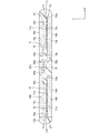
図2〜図12に示すように、半導体装置10は、IGBT11H,11L、封止樹脂体13、第1ヒートシンク14H,14L、ターミナル16、第2ヒートシンク18H,18L、継手部20、電源端子22、出力端子23、及び信号端子24を備えている。図4〜図11では、便宜上、後述する凹凸酸化膜30(粗化部)を省略している。
(Outline configuration of semiconductor device)
As shown in FIGS. 2 to 12, in the
半導体素子としてのIGBT11H,11Lは、Si、SiC、GaNなどの半導体基板に構成されている。本実施形態では、上記したようにIGBT11H,11Lがいずれもnチャネル型とされている。IGBT11H,11Lには、FWD12H,12Lも一体的に形成されている。詳しくは、IGBT11HにFWD12Hが形成され、IGBT11LにFWD12Lが形成されている。このように、IGBT11H,11Lとして、RC(Reverse Conducting)−IGBTを採用している。IGBT11Hが上アーム素子に相当し、IGBT11Lが下アーム素子に相当する。
The
IGBT11H,11Lは、Z方向に電流が流れるように縦型構造をなしている。IGBT11H,11Lには、上記したゲート電極11gもそれぞれ形成されている。ゲート電極11gはトレンチ構造をなしている。図4及び図5に示すように、IGBT11H,11Lの厚み方向、すなわちZ方向において、IGBT11H,11Lの一面にコレクタ電極11cがそれぞれ形成され、一面と反対の裏面にエミッタ電極11eがそれぞれ形成されている。コレクタ電極11cはFWD12H,12Lのカソード電極も兼ねており、エミッタ電極11eはFWD12H,12Lのアノード電極も兼ねている。コレクタ電極11cが一面側の主電極に相当し、エミッタ電極11eが裏面側の主電極に相当する。
The
IGBT11H,11Lは、互いにほぼ同じ平面形状、詳しくは平面略矩形状をなすとともに、互いにほぼ同じ大きさとほぼ同じ厚みを有している。IGBT11H,11Lは、互いに同じ構成となっている。IGBT11H,11Lは、お互いのコレクタ電極11cがZ方向における同じ側となり、お互いのエミッタ電極11eがZ方向における同じ側となるように配置されている。IGBT11H,11Lは、Z方向においてほぼ同じ高さに位置するとともに、X方向に横並びで配置されている。
The
図9に示すように、IGBT11H,11Lの裏面、すなわちエミッタ電極形成面には、信号用の電極であるパッド11pが形成されている。パッド11pは、エミッタ電極11eとは別の位置に形成されている。パッド11pは、エミッタ電極11eと電気的に分離されている。パッド11pは、Y方向において、エミッタ電極11eの形成領域とは反対側の端部に形成されている。
As shown in FIG. 9, a
本実施形態では、各IGBT11H,11Lが、それぞれ6つのパッド11pを有している。詳しくは、6つのパッド11pとして、ゲート電極11g用、ダミーゲート電極用、エミッタ電極11eの電位を検出するケルビンエミッタ用、電流センス用、IGBT11H,11Lの温度を検出する温度センサ(感温ダイオード)のアノード電位用、同じくカソード電位用を有している。6つのパッドは、平面略矩形状のIGBT11H,11Lにおいて、Y方向の一端側にまとめて形成されるとともに、X方向に並んで形成されている。なお、ダミーゲート電極とは、反転層(チャネル)の発生に寄与しないゲート電極である。
In this embodiment, each
封止樹脂体13は、IGBT11H,11Lを封止している。封止樹脂体13は、たとえばエポキシ系樹脂からなる。封止樹脂体13は、たとえばトランスファモールド法により成形されている。封止樹脂体13は、Z方向に直交する一面13aと、一面13aと反対の裏面13bと、一面13aと裏面13bとをつなぐ側面を有している。一面13a及び裏面13bは、たとえば平坦面となっている。
The sealing
第1ヒートシンク14H,14Lは、対応するIGBT11H,11Lの熱を半導体装置10の外部に放熱する機能を果たす。第1ヒートシンク14H,14Lは、配線としての機能も果たす。このため、熱伝導性及び電気伝導性を確保すべく、少なくとも金属材料を用いて形成されている。本実施形態では、第1ヒートシンク14H,14Lが、Z方向からの投影視において、対応するIGBT11H,11Lを内包するように設けられている。第1ヒートシンク14H,14Lは、対応するIGBT11H,11Lに対して、封止樹脂体13の一面13a側に配置されている。
The
第1ヒートシンク14H,14Lは、対応するIGBT11H,11Lのコレクタ電極11cと、はんだ15を介して接続されている。第1ヒートシンク14H,14Lが、第1放熱部に相当する。第1ヒートシンク14H,14Lそれぞれの大部分は封止樹脂体13によって覆われている。第1ヒートシンク14H,14Lの表面のうち、実装面14aにはんだ15が接続され、実装面14aとは反対の放熱面14bが、封止樹脂体13から露出されている。放熱面14bは、一面13aと略面一となっている。第1ヒートシンク14H,14Lの表面のうち、実装面14aの一部及び放熱面14bを除く部分は、封止樹脂体13によって覆われている。
The
詳しくは、第1ヒートシンク14Hの実装面14aに、IGBT11Hのコレクタ電極11cが、はんだ15を介して接続されている。第1ヒートシンク14Lの実装面14aに、IGBT11Lのコレクタ電極11cが、はんだ15を介して接続されている。第1ヒートシンク14H,14Lは、X方向に並んで配置されるとともに、Z方向においてほぼ同じ位置に配置されている。第1ヒートシンク14H,14Lの放熱面14bは、封止樹脂体13の一面13aから露出されるとともに、互いにX方向に並んでいる。
Specifically, the
ターミナル16は、対応するIGBT11H,11Lと第2ヒートシンク18H,18Lとの間に介在している。ターミナル16は、IGBT11H,11Lと第2ヒートシンク18H,18Lとの熱伝導、電気伝導経路の途中に位置するため、熱伝導性及び電気伝導性を確保すべく、少なくとも金属材料を用いて形成されている。ターミナル16は、エミッタ電極11eに対向配置され、はんだ17を介してエミッタ電極11eと接続されている。ターミナル16は、IGBT11H,11Lごとに設けられている。
The terminal 16 is interposed between the corresponding
第2ヒートシンク18H,18Lも、第1ヒートシンク14H,14L同様、対応するIGBT11H,11Lの熱を半導体装置10の外部に放熱する機能を果たす。第2ヒートシンク18H,18Lは、配線としての機能も果たす。本実施形態では、第2ヒートシンク18H,18Lが、Z方向からの投影視において、対応するIGBT11H,11Lを内包するように設けられている。第2ヒートシンク18H,18Lは、Z方向において、対応するIGBT11H,11Lに対し、封止樹脂体13の裏面13b側に配置されている。
Like the
第2ヒートシンク18H,18Lは、対応するIGBT11H,11Lのエミッタ電極11eと電気的に接続されている。詳しくは、第2ヒートシンク18H,18Lは、対応するエミッタ電極11eと、はんだ17、ターミナル16、及びはんだ19を介して、電気的に接続されている。第2ヒートシンク18H,18Lが、第2放熱部に相当する。第2ヒートシンク18H,18Lの大部分は封止樹脂体13によって覆われている。第2ヒートシンク18H,18Lの表面のうち、実装面18aにはんだ19が接続されており、実装面18aとは反対の放熱面18bが封止樹脂体13から露出されている。放熱面18bは、裏面13bと略面一となっている。第2ヒートシンク18H,18Lの表面のうち、実装面18aの一部及び放熱面18bを除く部分は、封止樹脂体13によって覆われている。
The
詳しくは、第2ヒートシンク18Hの実装面18aに、IGBT11Hに対応するターミナル16が、はんだ19を介して接続されている。第2ヒートシンク18Lの実装面18aに、IGBT11Lに対応するターミナル16が、はんだ19を介して接続されている。それぞれの実装面18aには、溢れたはんだ19を吸収するための溝18cが形成されている。溝18cは、Z方向からの投影視において、エミッタ電極11e、すなわちターミナル16を取り囲むように環状に形成されている。
Specifically, the terminal 16 corresponding to the
第2ヒートシンク18H,18Lは、X方向に並んで配置されるとともに、Z方向においてほぼ同じ位置に配置されている。そして、第2ヒートシンク18H,18Lの放熱面18bが、封止樹脂体13の裏面13bから露出されるとともに、互いにX方向に並んでいる。本実施形態では、第2ヒートシンク18H,18Lを共通部材としており、第2ヒートシンク18Hと第2ヒートシンク18Lとの配置はZ軸を回転軸とする2回対称となっている。第2ヒートシンク18H,18Lは、Y方向の側面18d,18eを有している。第2ヒートシンク18Hにおいて側面18dが側面14cに対応しており、第2ヒートシンク18Lにおいて側面18eが側面14cに対応している。このため、第2ヒートシンク18Hの側面18d及び第2ヒートシンク18Lの側面18eが、第2側面に相当する。第2ヒートシンク18Hの側面18d及び第2ヒートシンク18Lの側面18eは、Y方向において側面14cと同じ側の面であり、Y方向に延びる部材が連なっていない。
The
継手部20は、第1継手部20a、第2継手部20b、及び第3継手部20cを有している。第1継手部20a及び第3継手部20cは、上アーム側の第2ヒートシンク18Hと、下アーム側の第1ヒートシンク14Lとを電気的に接続している。図5及び図10に示すように、第2継手部20bは、下アーム側の第2ヒートシンク18Lと負極端子22nとを電気的に接続している。
The joint portion 20 has a first
本実施形態において、第1継手部20aは、同一の金属板を加工することで第2ヒートシンク18Hと一体的に設けられている。また、第2継手部20bは、同一の金属板を加工することで第2ヒートシンク18Lと一体的に設けられている。第1継手部20aを含む第2ヒートシンク18Hと、第2継手部20bを含む第2ヒートシンク18Lとを共通部材としており、半導体装置10においてこれらの配置は、Z軸を回転軸とする2回対称となっている。
In the present embodiment, the first
第1継手部20aは、封止樹脂体13に被覆されるように、第2ヒートシンク18Hよりも薄く設けられている。第1継手部20aは、第2ヒートシンク18Hの実装面18aと略面一となるように、第2ヒートシンク18Hに連なっている。第1継手部20aは、薄板状をなしており、第2ヒートシンク18Hにおける第2ヒートシンク18L側の側面からX方向に延びている。第1継手部20a及び第2ヒートシンク18Hを有する部材において、第2ヒートシンク18Hは、エミッタ電極11eと接続され、放熱機能を果たす厚肉部に相当し、第1継手部20aは、厚肉部よりも薄くされ、電気的な中継機能を果たす薄肉部に相当する。薄肉部である第1継手部20aは、厚肉部である第2ヒートシンク18Hの側面からX方向に延設されており、Y方向に延設されていない。第1継手部20aにおいて、第2ヒートシンク18Hの実装面18aに連なる面には、はんだ21を介して第3継手部20cが接続されている。
The first
第2継手部20bも、封止樹脂体13に被覆されるように、第2ヒートシンク18Lよりも薄く設けられている。第2継手部20bは、第2ヒートシンク18Lの実装面18aと略面一となるように、第2ヒートシンク18Lに連なっている。第2継手部20bは、薄板状をなしており、第2ヒートシンク18Lにおける第2ヒートシンク18L側の側面からX方向に延びている。
The second
第2継手部20b及び第2ヒートシンク18Lを有する部材において、第2ヒートシンク18Lは、エミッタ電極11eと接続され、放熱機能を果たす厚肉部に相当し、第2継手部20bは、厚肉部よりも薄くされ、電気的な中継機能を果たす薄肉部に相当する。薄肉部である第2継手部20bは、厚肉部である第2ヒートシンク18Lの側面からX方向に延設されており、Y方向に延設されていない。第2継手部20bにおいて、第2ヒートシンク18Lの実装面18aに連なる面には、はんだ21を介して負極端子22nが接続されている。
In the member having the second
第1継手部20a及び第2継手部20bそれぞれの実装面18aに連なる面には、溢れたはんだ21を吸収するための溝20dが形成されている。溝20dは、環状に形成されている。以下において、第1継手部20a及び第2継手部20bを、単に継手部20a,20bとも称する。
A
本実施形態では、はんだ15,17,19,21として、Niボール入りのはんだを採用している。Niボールとしては、超音波探傷装置(SAT:Scanning Acoustic Tomograph)での検査が可能なはんだ厚を確保できる直径、たとえば40μm以上を有していればよい。これにより、はんだ15,17,19,21のいずれについても、たとえばボイドの検出が可能となる。
In this embodiment, solder containing Ni balls is used as the
第3継手部20cも、同一の金属板を加工することで第1ヒートシンク14Lと一体的に設けられている。第3継手部20cは、封止樹脂体13に被覆されるように、第1ヒートシンク14Lよりも薄く設けられている。第3継手部20cは、第1ヒートシンク14Lの実装面14aに略面一で連なっている。第3継手部20cは、第1ヒートシンク14Lにおける第1ヒートシンク14H側の側面から、第2ヒートシンク18Hに向けて延設されている。
The third
第3継手部20cは、Z方向からの平面視において、X方向に延設されている。本実施形態では、図4に示すように、第3継手部20cが屈曲部を2箇所有している。第3継手部20cの先端部分は、Z方向からの投影視において、第1継手部20aと重なっている。そして、第3継手部20cと第1継手部20aとが、はんだ21を介して接続されている。第3継手部20cは、Y方向において、第2継手部20bと横並びとなるように設けられている。
The third
なお、第1継手部20aを、第2ヒートシンク18Hとは別部材とし、第2ヒートシンク18Hに接続することで第2ヒートシンク18Hに連なる構成としてもよい。第2継手部20bを、第2ヒートシンク18Lとは別部材とし、第2ヒートシンク18Lに接続することで第2ヒートシンク18Lに連なる構成としてもよい。また、第3継手部20cを、第1ヒートシンク14Lとは別部材とし、第1ヒートシンク14Lに接続することで第1ヒートシンク14Lに連なる構成としてもよい。第1継手部20a及び第3継手部20cの一方のみにより、上アームと下アームとを電気的に接続することもできる。
The first
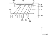
電源端子22は、正極端子22p及び負極端子22nを有している。正極端子22pは、平滑コンデンサ4の正極側の端子と電気的に接続される。正極端子22pは、正極側ライン6と電気的に接続される。正極端子22pは、主電流が流れる主端子である。正極端子22pは、高電位電源端子、P端子とも称される。正極端子22pは、第1ヒートシンク14Hに連なっており、第1ヒートシンク14Hの側面のうち、Y方向において信号端子24側の面とは反対の側面14cからY方向に延設されている。正極端子22pが延設部又は第1主端子に相当し、側面14cが第1側面に相当する。本実施形態では、同一の金属板を加工することで、正極端子22pが第1ヒートシンク14Hと一体的に設けられている。正極端子22pは、第1ヒートシンク14HにおけるY方向の一端に連なっている。正極端子22pは、Y方向に延設され、図3に示すように、封止樹脂体13の側面13cから外部に突出している。
The
第1ヒートシンク14H及び正極端子22pを構成する金属板として異形条を採用しており、正極端子22pは薄板状をなしている。正極端子22p及び第1ヒートシンク14Hを有する部材において、第1ヒートシンク14Hは、コレクタ電極11cと接続され、放熱機能を果たす厚肉部に相当し、正極端子22pは、厚肉部よりも薄くされ、電気的な中継機能を果たす薄肉部に相当する。薄肉部である正極端子22pは、厚肉部である第1ヒートシンク14Hの側面14cからY方向に延設され、封止樹脂体13の側面13cから突出している。
A deformed strip is used as the metal plate constituting the
負極端子22nは、平滑コンデンサ4の負極側の端子と電気的に接続される。負極端子22nは、負極側ライン7と電気的に接続される。負極端子22nは、主電流が流れる主端子である。負極端子22nは、低電位電源端子、N端子とも称される。負極端子22nは、その一部が、Z方向からの投影視において第3継手部20cと重なるように配置されている。負極端子22nは、Z方向において、第3継手部20cよりもIGBT11Lに近い位置に配置されている。負極端子22nと第3継手部20cも、はんだ21を介して接続されている。
The
負極端子22nは、Y方向に延設されて、正極端子22pと同じ側面13cから外部に突出している。図5及び図6などに示すように、負極端子22nのうち、第2継手部20bとの接続部分の厚みは、他の部分の厚み、たとえば封止樹脂体13から外に突出した部分の厚みよりも厚くされている。
The
出力端子23は、上下アームの接続点と電気的に接続される。出力端子23は、主電流が流れる主端子である。出力端子23は、モータ3の対応する相のコイル(固定子巻線)と電気的に接続される。出力端子23は、交流端子、O端子とも称される。出力端子23は、第1ヒートシンク14Lに連なっており、第1ヒートシンク14Lの側面のうち、Y方向において信号端子24側の面とは反対の側面14cから、Y方向であって正極端子22pと同じ側に延設されている。出力端子23が延設部又は第2主端子に相当し、第1ヒートシンク14Lの側面14cが第1側面に相当する。
The
本実施形態では、同一の金属板を加工することで、出力端子23が第1ヒートシンク14Lと一体的に設けられている。出力端子23は、第1ヒートシンク14LにおけるY方向の一端に連なっている。出力端子23は、Y方向に延設されて、正極端子22p及び負極端子22nと同じ側面13cから外部に突出している。
In the present embodiment, the
第1ヒートシンク14L及び出力端子23を構成する金属板として異形条を採用しており、出力端子23は薄板状をなしている。出力端子23及び第1ヒートシンク14Lを有する部材において、第1ヒートシンク14Lは、コレクタ電極11cと接続され、放熱機能を果たす厚肉部に相当し、出力端子23は、厚肉部よりも薄くされ、電気的な中継機能を果たす薄肉部に相当する。薄肉部である出力端子23は、厚肉部である第1ヒートシンク14Lの側面14cからY方向に延設され、封止樹脂体13の側面13cから突出している。
A deformed strip is adopted as the metal plate constituting the
正極端子22p、負極端子22n、及び出力端子23それぞれの封止樹脂体13からの突出部分は、Z方向において互いにほぼ同じ位置に配置されている。また、X方向において、正極端子22p、負極端子22n、及び出力端子23の順に並んで配置されている。このように、正極端子22pの隣りに、負極端子22nが配置されている。
The protruding portions of the
正極端子22p、負極端子22n、及び出力端子23は、少なくとも封止樹脂体13から突出部分において略平板状とされ、Z方向の厚みが互いに略等しくされている。よって、正極端子22p、負極端子22n、及び出力端子23それぞれの突出部分の厚みが、互いに略等しくされている。また、正極端子22p、負極端子22n、及び出力端子23それぞれの突出部分の幅が、互いに略等しくされている。ここで、幅とは、側面13cからの突出方向であるY方向及び板厚方向であるZ方向の両方向に直交する方向、すなわちX方向の長さである。
The
また、正極端子22pの突出長さが、負極端子22nの突出長さよりも短くされている。ここで、突出長さとは、封止樹脂体13の側面13cを位置の基準として、外部に延設された長さである。本実施形態では、出力端子23の突出長さが、負極端子22nの突出長さよりも長くされている。すなわち、突出長さは、正極端子22pが最も短くされ、出力端子23が最も長くされている。負極端子22nの突出長さは、中間の長さとされている。
Further, the protruding length of the
なお、正極端子22pを、第1ヒートシンク14Hとは別部材とし、第1ヒートシンク14Hに接続することで第1ヒートシンク14Hに連なる構成としてもよい。負極端子22nを、第3継手部20c、ひいては第2ヒートシンク18Lと同一の金属板から構成してもよい。出力端子23を、第1ヒートシンク14Lとは別部材とし、第1ヒートシンク14Lに接続することで第1ヒートシンク14Lに連なる構成としてもよい。
The
電源端子22及び出力端子23には、後述する冷却器との積層状態で、図示しないバスバーがそれぞれ接続される。バスバーは、正極側ライン6、負極側ライン7、出力ライン8を構成する。バスバーは、たとえばレーザ溶接により、対応する電源端子22、出力端子23と接続される。
Bus bars (not shown) are connected to the
信号端子24は、図7〜図9に示すように、対応するIGBT11H,11Lのパッド11pに、ボンディングワイヤ25を介して電気的に接続されている。本実施形態では、アルミニウム系のボンディングワイヤ25を採用している。信号端子24は、Y方向に延設されており、図3に示すように、封止樹脂体13において側面13cとは反対の側面13dから外部に突出している。
As shown in FIGS. 7 to 9, the
半導体装置10は、IGBT11H用に5本の信号端子24を有し、IGBT11L用に5本の信号端子24を有している。それぞれの5本の信号端子24のうち、1本の信号端子24aは、残りの信号端子24bよりもボンディングワイヤ25が接続される領域のX方向の幅が広くされている。信号端子24aには、エミッタ電極11eの電位を検出するケルビンエミッタ用のパッド11pとダミーゲート電極用のパッド11pが、それぞれボンディングワイヤ25を介して接続されている。これにより、ダミーゲート電極がエミッタ電位に固定されている。ゲート電極11g用、電流センス用、温度センサのアノード電位用、カソード電位用のパッド11pについては、互いに異なる信号端子24bに接続されている。
The
図6などに示すように、本実施形態では、第1ヒートシンク14H,14L、第3継手部20c、正極端子22p、負極端子22n、出力端子23、及び信号端子24が、同一の金属板であるリードフレーム26から構成されている。リードフレーム26は、上記以外にも、外枠26a、吊りリード26b、及びタイバー26cなどを有している。リードフレーム26において、第1ヒートシンク14H,14L及び負極端子22nの一部分が厚肉部とされており、それ以外の部分は厚肉部よりも厚みの薄い薄肉部とされている。
As shown in FIG. 6 and the like, in the present embodiment, the
Y方向において、第1ヒートシンク14Hは、側面14cから延設された正極端子22pを介して外枠26aに連結されている。第1ヒートシンク14Lも、側面14cから延設された出力端子23を介して外枠26aに連結されている。また、第1ヒートシンク14H,14Lにおける側面14cと反対の側面14dには、吊りリード26bが連なっている。吊りリード26bは、側面14dからY方向に延設され、外枠26aに連結されている。
In the Y direction, the
主端子である正極端子22p、負極端子22n、及び出力端子23は、Y方向においてそれぞれの一端が外枠26aに連なっている。また、X方向に延びるタイバー26cにより、相互に連結されている。信号端子24は、タイバー26cにより、外枠26a及び吊りリード26bに連結されている。信号端子24において、ボンディングワイヤ25が接続される端部とは反対の端部は、外枠26aに連結されておらず、フリーとなっている。
One ends of the
以上のように構成される半導体装置10では、封止樹脂体13により、IGBT11H,11L、第1ヒートシンク14H,14Lそれぞれの一部、ターミナル16、第2ヒートシンク18H,18Lそれぞれの一部、電源端子22それぞれの一部、出力端子23の一部、及び信号端子24の一部が、一体的に封止されている。半導体装置10では、封止樹脂体13によって、一相分の上下アームを構成する2つのIGBT11H,11Lが封止されている。このため、半導体装置10は、2in1パッケージとも称される。
In the
第1ヒートシンク14H,14Lそれぞれの放熱面14bは、同一面内に位置するとともに、封止樹脂体13の一面13aと略面一となっている。同じく、第2ヒートシンク18H,18Lそれぞれの放熱面18bは、同一面内に位置するとともに、封止樹脂体13の裏面13bと略面一となっている。このように、半導体装置10は、放熱面14b,18bがともに封止樹脂体13から露出された両面放熱構造をなしている。
The
(半導体装置10の製造方法)
製造方法の概略について説明する。先ず、半導体装置10を構成する各要素を準備する。たとえば図6に示すリードフレーム26を準備する。また、IGBT11H,11L、ターミナル16、第1継手部20aを含む第2ヒートシンク18H、第2継手部20bを含む第2ヒートシンク18Lをそれぞれ準備する。第2ヒートシンク18H,18Lは、上記したように共通部材である。
(Manufacturing method of semiconductor device 10)
The outline of the manufacturing method will be described. First, each element constituting the
次いで、リードフレーム26における第1ヒートシンク14H,14Lの実装面14a上に、はんだ15を介して、対応するIGBT11H,11Lを配置する。その際、コレクタ電極11cが実装面14aと対向するように、IGBT11H,11Lを配置する。次に、たとえば予め両面にはんだ17,19が迎えはんだとして配置されたターミナル16を、はんだ17がIGBT11H,11L側となるように配置する。はんだ19については、半導体装置10における高さばらつきを吸収可能な量、配置しておく。また、第3継手部20c及び負極端子22n上にはんだ21を配置しておく。
Next, the corresponding
そして、この積層状態で、はんだの1stリフローを実施する。これにより、はんだ15を介して、IGBT11H,11Lのコレクタ電極11cと対応する第1ヒートシンク14H,14Lとが接続される。また、はんだ17を介して、IGBT11H,11Lのエミッタ電極11eと対応するターミナル16とが接続される。すなわち、リードフレーム26、IGBT11H,11L、及びターミナル16が一体化された接続体を得ることができる。リフロー後、IGBT11H,11Lのパッド11pと信号端子24を、ボンディングワイヤ25により接続する。図7、図8、図9は、ボンディング後の接続体を示している。
Then, in this laminated state, the 1st reflow of the solder is performed. As a result, the
次いで、実装面18aが上になるようにして第2ヒートシンク18H,18Lを図示しない台座上に配置する。そして、ターミナル16が第2ヒートシンク18H,18Lに対向するように、接続体を第2ヒートシンク18H,18L上に配置し、はんだの2ndリフローを実施する。2ndリフローでは、第1ヒートシンク14H,14L側から荷重を加えることで、半導体装置10の高さが所定高さとなるようにする。詳しくは、図示しないスペーサを、第1ヒートシンク14H,14Lと台座との間に配置し、スペーサを、第1ヒートシンク14H,14Lと台座の両方に接触させる。このようにして、半導体装置10の高さが所定高さとなるようにする。図10は、2ndリフロー後の状態を示している。
Next, the
次いで、トランスファモールド法により封止樹脂体13の成形を行う。本実施形態では、第1ヒートシンク14H,14L及び第2ヒートシンク18H,18Lが完全に被覆されるように、封止樹脂体13を成形する。図11は、成形後の状態を示している。
Next, the sealing
次いで、成形した封止樹脂体13を第1ヒートシンク14H,14Lの一部ごと切削することにより、第1ヒートシンク14H,14Lの放熱面14bを露出させる。これにより、放熱面14bは一面13aと略面一となる。同じく、封止樹脂体13を第2ヒートシンク18H,18Lの一部ごと切削することにより、第2ヒートシンク18H,18Lの放熱面18bを露出させる。これにより、放熱面18bは裏面13bと略面一となる。
Next, the heat-dissipating
図12は、切削後の状態を示している。なお、放熱面14b,18bを成形金型のキャビティ壁面に押し当て、密着させた状態で、封止樹脂体13を成形してもよい。この場合、封止樹脂体13を成形した時点で、放熱面14b,18bが封止樹脂体13から露出される。このため、成形後の切削が不要となる。
FIG. 12 shows the state after cutting. The sealing
次いで、外枠26a及びタイバー26cなど、リードフレーム26の不要部分を除去する。これにより、半導体装置10を得ることができる。
Next, unnecessary parts of the
(冷却器との積層構造)
図13に示すように、半導体装置10は、冷却器50と交互に積層され、冷却器50とともにパワーモジュールを構成する。冷却器50は、内部に冷媒が流通され、Z方向において各半導体装置10の両面側にそれぞれ配置されて、半導体装置10を両面側から冷却する。冷却器50は、冷媒が流れる通路を内部に有するように、管状(チューブ状)に形成されている。また、Z方向において、半導体装置10と冷却器50とが交互に積層されるように、隣り合う冷却器50の間に所定間隔を有して配置されている。このように,Z方向が、積層方向に相当する。
(Laminate structure with cooler)
As shown in FIG. 13, the
冷却器50は、X方向の一端側で、上流側連結部51により、隣り合う冷却器50同士が連結されている。上流側連結部51は、供給された冷媒を、各冷却器50に分配する機能を果たす。一方、X方向の他端側で、下流側連結部52により、隣り合う冷却器50同士が連結されている。この下流側連結部52は、各冷却器50に分配された冷媒を合流させる機能を果たす。
The cooler 50 is one end side in the X direction, and
図13に示すパワーモジュールは、インバータ5の三相分の上下アームを構成する3つの半導体装置10と、各半導体装置10を両面側から冷却するように、半導体装置10と交互に積層された複数の冷却器50を備えている。半導体装置10は、Z方向において冷却器50によって挟まれている。封止樹脂体13の大部分は、隣り合う冷却器50の対向領域内に配置されている。正極端子22p、負極端子22n、及び出力端子23は、対応するバスバーとの接続のため、対向領域の外まで延設されている。
The power modules shown in FIG. 13 include three
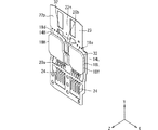
(凹凸酸化膜)
図14及び図15は、第1継手部20aを含む第2ヒートシンク18Hを示している。第2ヒートシンク18Hには、表面が連続して凹凸をなす凹凸酸化膜30が形成されている。このように、半導体装置10は、凹凸酸化膜30を備えている。凹凸酸化膜30は、レーザ光を照射することで形成されている。第2継手部20bを含む第2ヒートシンク18Lも、共通構造であるため、同様の構成となっている。以下では、第2ヒートシンク18Hを例に説明する。
(Concave and convex oxide film)
14 and 15 show a
図14及び図15に示すように、凹凸酸化膜30は、第2ヒートシンク18Hの実装面18aと側面18d,18eにそれぞれ形成されている。半導体装置10は、凹凸酸化膜30による粗化部として、実装面粗化部31及び側面粗化部32を有している。明確化のため、図14では、凹凸酸化膜30の形成領域にハッチングを施している。
As shown in FIGS. 14 and 15, the
実装面粗化部31は、実装面18aに凹凸酸化膜30が形成されてなる。実装面18aにおいて、溝18c及び溝18cよりも内側の領域には、凹凸酸化膜30が形成されていない。図14及び図15に破線で示す境界31aは、凹凸酸化膜30の形成領域と非形成領域との境界を示している。境界31aは、環状をなす溝18cの外周に大部分でほぼ一致している。境界31aは、外周の一部分に対して、それよりも外側に設定されている。具体的には、四隅が丸められた略矩形環状の溝18cに対し、四隅のひとつについては、その外周部分に境界31aが一致せず、外周部分よりも外側に境界31aが設定されている。このように、本実施形態では、溝18cの外周と境界31aとの間に、凹凸酸化膜30の形成されていない非粗化領域31bを意図的に設けている。
The mounting surface roughened
カメラ等の撮像手段によってレーザ光による粗化の位置ずれを検査する際、境界31a、すなわち実装面粗化部31の輪郭のすべてが溝18c内に入ると、ピントが合わず、輪郭を認識できなくなる。このため、位置ずれが生じても検出できない。これに対し、本実施形態では、溝18cの外周と境界31aとの間に非粗化領域31bを設けているため、確実に位置ずれを検査することができる。
When inspecting the misalignment of roughening due to laser light by an imaging means such as a camera, if all the contours of the
また、実装されるIGBT11H,11Lのサイズが異なり、これにより溝18cの大きさが異なる複数の品番を検査する際に、誤ったパターンでの粗化を検出することも可能となる。たとえば、サイズ大用のパターンで粗化すべきところ、誤ってサイズ小用のパターンで粗化したとしても、非粗化領域31bの少なくとも一部が溝18c外となるため、位置ずれ検査と合わせて粗化パターン間違えも検査することができる。
Further, when inspecting a plurality of product numbers having different sizes of the mounted
本実施形態では、第2ヒートシンク18Hの実装面18aだけでなく、第2ヒートシンク18に連なる第1継手部20aの実装面にも、実装面粗化部31が一体的に形成されている。第1継手部20aにおいて、凹凸酸化膜30は、溝20d及び溝20dよりも内側の領域には、形成されておらず、溝20dの全周で上記した境界が溝20dの外周とほぼ一致している。
In the present embodiment, the mounting surface roughened
側面粗化部32は、側面18d,18eのそれぞれに凹凸酸化膜30が形成されてなる。側面粗化部32は、第2ヒートシンク18Hの側面のうち、側面18d,18eのみに形成されている。本実施形態では、第2ヒートシンク18Hに連なる第1継手部20aにも、側面粗化部32が一体的に形成されている。第1継手部20aにおいて、凹凸酸化膜30は、側面18dに連なる面に形成されている。第2ヒートシンク18Hの側面18d,18e及び該側面18dに連なる第1継手部20aの面それぞれの全面が、側面粗化部32とされている。
The side surface roughened
図16に示すように、凹凸酸化膜30は、基材33上に形成された皮膜34の一部である。基材33は、第1継手部20aを含む第2ヒートシンク18Hを構成するCuなどの金属部材である。皮膜34は、基材33の表面に形成された金属薄膜35と、凹凸酸化膜30を有している。
As shown in FIG. 16, the
本実施形態において、金属薄膜35はNiを主成分とする膜を少なくとも含んでいる。金属薄膜35は、たとえばめっき、蒸着により形成されたものである。金属薄膜35は、たとえば無電解Niめっき膜を含んでいる。
In the present embodiment, the metal
金属薄膜35は、基材33の表面のうち、第2ヒートシンク18Hの放熱面18bを除く部分に形成されている。金属薄膜35の表面のうち、実装面粗化部31の形成部分、及び、側面粗化部32の形成部分には、複数の凹部35aが形成されている。凹部35aが形成されていない部分において、金属薄膜35の膜厚は、たとえば10μm程度とされる。換言すれば、後述するレーザ光の照射前の膜厚が、10μm程度とされる。
The metal
凹部35aは、パルス発振のレーザ光の照射により形成されている。1パルスごとに1つの凹部35aが形成される。凹部35aは、レーザ光の照射痕である。レーザ光の走査方向において、隣り合う凹部35aが連なっている。実装面粗化部31及び側面粗化部32の形成部分において、金属薄膜35の表面は、複数の凹部35aにより鱗状をなしている。
The
各凹部35aの幅は、5μm〜300μmとされている。凹部35aの深さは、0.5μm〜5μmとされている。凹部35aの深さが0.5μmより浅いと、レーザ光の照射による金属薄膜35の表面の溶融及び蒸着が不十分となり、凹凸酸化膜30が形成され難くなる。凹部35aの深さが5μmよりも深いと、金属薄膜35の表面が溶融飛散しやすくなり、蒸着よりも溶融飛散による表面形成が支配的となり、凹凸酸化膜30が形成され難くなる。
The width of each
凹凸酸化膜30は、金属薄膜35を構成する主成分金属と同じ金属の酸化物の膜である。凹凸酸化膜30は、金属薄膜35にレーザ光を照射することで、金属薄膜35を構成する金属を酸化して形成されている。凹凸酸化膜30は、金属薄膜35の表層を酸化することで、金属薄膜35の表面に形成された酸化物の膜である。凹凸酸化膜30は、レーザ光の照射により形成されるため、レーザ照射膜とも言える。
The concave-
本実施形態では、凹凸酸化膜30を構成する成分のうち、80%がNI2O3、10%がNiO、10%がNiとなっている。このように、凹凸酸化膜30の主成分は、金属薄膜35の主成分であるNiの酸化物である。
In the present embodiment, 80% of the components constituting the
凹凸酸化膜30は、金属薄膜35の表面のうち、凹部35aの表面に形成されている。凹凸酸化膜30の平均膜厚は、10nm〜数百nmとされている。凹凸酸化膜30は、凹部35aを有する金属薄膜35の表面の凹凸に倣って形成されている。また、凹凸酸化膜30の表面には、凹部35aの幅よりも細かいピッチで凹凸が形成されている。すなわち、非常に微細な凹凸(粗化部)が形成されている。換言すれば、複数の凸部30a(柱状体)が、細かいピッチで形成されている。たとえば凸部30aの平均幅は1nm〜300nm、凸部30a間の平均間隔は1nm〜300nmとされている。また、凸部30aの平均高さは、10nm〜数百nmとされている。
The
このように、表面に非常に微細な凹凸が形成された凹凸酸化膜30により、実装面粗化部31及び側面粗化部32が形成されている。凹凸酸化膜30を有すると、凹凸酸化膜30を有さない構成、すなわち金属薄膜35の表面が露出する構成に比べて、はんだに対する濡れ性を低下させることができる。このため、実装面粗化部31により、はんだ19,21の濡れ拡がりを抑制することができる。
As described above, the mounting surface roughened
また、凹凸酸化膜30の表面の凸部30aに封止樹脂体13が絡みつき、アンカー効果が生じる。凹凸により、封止樹脂体13との接触面積が増える。これにより、実装面粗化部31及び側面粗化部32のそれぞれに、封止樹脂体13が密着する。したがって、封止樹脂体13の剥離を抑制することができる。
Further, the sealing
なお、凹凸酸化膜30については、以下の方法によって形成することができる。まず、上記した金属薄膜35が形成された第2ヒートシンク18Hを準備する。
The
次に、レーザ光を照射して凹凸酸化膜30を形成する。第2ヒートシンク18Hの実装面18a及び側面18d,18eのそれぞれに、パルス発振のレーザ光を照射することにより、金属薄膜35の表面を溶融及び蒸発させる。具体的には、レーザ光を照射することにより、金属薄膜35の表面の部分を溶融させるとともに、蒸発(気化)させて、外気中に浮遊させる。
Next, the
パルス発振のレーザ光は、エネルギー密度が0J/cm2より大きく100J/cm2以下で、パルス幅が1μ秒以下となるように調整される。この条件を満たすには、YAGレーザ、YVO4レーザ、ファイバレーザなどを採用することができる。たとえばYAGレーザの場合、エネルギー密度が1J/cm2以上であればよい。無電解Niめっきの場合、たとえば5J/cm2程度でも金属薄膜35を加工することができる。
Pulsed laser light energy density is large 100 J / cm 2 or less than 0 J / cm 2, the pulse width is adjusted to be equal to or less than 1μ seconds. This condition is satisfied, it is possible to adopt a YAG laser, YVO 4 laser, such as a fiber laser with. For example, in the case of a YAG laser, the energy density may be 1 J / cm 2 or more. In the case of electroless Ni plating, the metal
このとき、レーザ光の光源と第2ヒートシンク18Hとを相対的に移動させることにより、レーザ光を複数の位置に順に照射する。レーザ光を照射し、金属薄膜35の表面を溶融、気化させることで、金属薄膜35の表面には、凹部35aが形成される。金属薄膜35のうち、レーザ光を照射した部分の平均厚みは、レーザ光を照射しない部分の平均厚みよりも薄くなる。また、レーザ光のスポットに対応して形成される複数の凹部35aは、X方向において連なるとともに、Y方向においても連なる。これにより、レーザ照射痕である凹部35aは、たとえば鱗状となる。
At this time, by relatively moving the light source of the laser beam and the
次いで、溶融した金属薄膜35の部分を凝固させる。具体的には、溶融して気化した金属薄膜35を、レーザ光が照射された部分やその周辺部分に蒸着させる。このように、溶融して気化した金属薄膜35を蒸着させることにより、金属薄膜35の表面上に凹凸酸化膜30を形成する。凹凸酸化膜30は、主として、金属薄膜35におけるレーザ光が照射された部分に形成される。
Next, the portion of the molten metal
なお、レーザ光の照射において、エネルギー密度を100J/cm2よりも大きくすると、凹凸酸化膜30が形成されない。また、パルス発振ではなく、連続発振のレーザ光を照射した場合にも、凹凸酸化膜30が形成されない。
When the energy density is made larger than 100 J / cm 2 in the irradiation of the laser beam, the
(半導体装置の効果)
図17は、比較例を示している。比較例の符号として、本実施形態に示した関連する要素の符号に100を加算したもの付与している。比較例では、図示しないが、第2ヒートシンク118H,118Lの実装面のみに、凹凸酸化膜が形成されている。すなわち、実装面粗化部のみを有している。半導体装置110はZ方向において冷却器に挟まれ、冷却器への取り付け状態で半導体装置110に応力が作用する。半導体装置110では、第2ヒートシンク118及び図中に表れていない第1ヒートシンクのうち、第1ヒートシンクのみに、Y方向の側面からY方向に延設されて封止樹脂体113から突出する延設部としての正極端子22p、出力端子123が設けられている。このため、第2ヒートシンク118Hの側面118dと封止樹脂体113との境界部分、第2ヒートシンク118Hの側面118eと封止樹脂体113との境界部分に応力が集中する。このような応力集中により、封止樹脂体113に図中に例示するようなクラック200(割れ)が生じる虞がある。クラック200は、裏面113b側においてX方向に沿って生じる虞がある。
(Effect of semiconductor device)
FIG. 17 shows a comparative example. As a code of the comparative example, a code obtained by adding 100 to the code of the related element shown in the present embodiment is given. In the comparative example, although not shown, the uneven oxide film is formed only on the mounting surfaces of the
これに対し、本実施形態では、凹凸酸化膜30による粗化部として、実装面粗化部31に加えて、側面粗化部32を有している。側面粗化部32は、図18に示すように、第2ヒートシンク18Hにおいて、延設部が連なる側面14cに対応する側面18dに形成されている。また、第2ヒートシンク18Lにおいて、延設部が連なる側面14cに対応する側面18eに形成されている。側面粗化部32を設けることで、冷却器50との積層構造において応力が集中する側面と封止樹脂体13との境界部分の密着性が従来よりも高くなっている。したがって、封止樹脂体13との密着性の高い部分を局所的に設けつつも、冷却器50との積層により応力が作用する半導体装置10において、封止樹脂体13にクラックが生じるのを抑制することができる。
On the other hand, in the present embodiment, as the roughened portion by the
特に本実施形態では、第1ヒートシンク14H,14Lの側面14cに、延設部として正極端子22p、出力端子23が連なっている。正極端子22p及び出力端子23はバスバーと接続されるため、第1ヒートシンク14H,14Lが積層の応力を受けて変形し難い。その分、応力は第2ヒートシンク18Hの側面18dと封止樹脂体13との境界部分、第2ヒートシンク18Hの側面18eと封止樹脂体13との境界部分に集中する。しかしながら、凹凸酸化膜30による側面粗化部32により、クラックが生じるのを抑制することができる。
In particular, in the present embodiment, the
本実施形態では、IGBT11H,11LがX方向において並んで配置されており、これにより第1ヒートシンク14H,14L、第2ヒートシンク18H,18LもX方向に並んで配置されている。この横並び配置により、延設部である正極端子22p、出力端子23の延設方向と直交するX方向において、封止樹脂体13の長さが長くなっている。このため、第2ヒートシンク18Hの側面18dと封止樹脂体13との境界部分、第2ヒートシンク18Hの側面18eと封止樹脂体13との境界部分に応力が集中しやすい。しかしながら、凹凸酸化膜30による側面粗化部32により、クラックが生じるのを抑制することができる。特に、第2ヒートシンク18H,18Lの両方に側面粗化部32を設けているため、いずれかに応力が偏って作用しても、クラックが生じるのを抑制することができる。
In the present embodiment, the
本実施形態では、第2ヒートシンク18H,18Lに連なる継手部20a,20bの側面にも、側面粗化部32が設けられている。このように、厚肉部である第2ヒートシンク18H,18Lに連なる薄肉部にも側面粗化部32が設けられているため、クラックが生じるのを効果的に抑制することができる。
In the present embodiment, the side
本実施形態では、第1ヒートシンク14H,14Lの側面14dには、延設部としての吊りリード26bが連なっている。吊りリード26bは、冷却器50との積層構造において、自由端である。これに対し、第2ヒートシンク18H,18Lにおいて、Y方向の側面18d,18eの両方に側面粗化部32を設けている。すなわち、第2ヒートシンク18Hの側面18eと、第2ヒートシンク18Hの側面18dにも、側面粗化部32を設けている。したがって、第2ヒートシンク18Hの側面18eと封止樹脂体13との境界部分、第2ヒートシンク18Hの側面18dと封止樹脂体13との境界部分に応力が集中しても、クラックが生じるのを抑制することができる。
In the present embodiment, the hanging leads 26b as an extension portion are connected to the side surfaces 14d of the
なお、第2ヒートシンク18H,18Lを共通部材とする例を示したが、これに限定されない。互いに異なる部材を採用し、第2ヒートシンク18Hにおいて側面18dのみ、第2ヒートシンク18Lにおいて側面18eのみに、側面粗化部32を設けてもよい。
Although an example in which the
また、第2ヒートシンク18H,18Lの実装面18aに凹凸酸化膜30(実装面粗化部31)を設ける例を示したがこれに限定されない。実装面18aに加えて、第1ヒートシンク14H,14Lの実装面14aに凹凸酸化膜30を設けてもよい。リードフレーム26において実装面18a側の面のうち、封止樹脂体13に封止される部分であって、実装部分を除く部分に凹凸酸化膜30を設けてもよい。
Further, an example is shown in which the uneven oxide film 30 (mounting surface roughened portion 31) is provided on the mounting
(第2実施形態)
本実施形態は、先行実施形態を参照できる。このため、先行実施形態に示した半導体装置10と共通する部分についての説明は省略する。
(Second Embodiment)
In this embodiment, the preceding embodiment can be referred to. Therefore, the description of the parts common to the
下アーム側の第2ヒートシンク18Lに連なる第2継手部20bは、負極端子22nと接続されている。負極端子22nの接続により、第2ヒートシンク18Lは変形し難くなり、負極端子22nにバスバーに接続されることでさらに変形し難くなる。
The second
一方、上アーム側の第2ヒートシンク18Hに連なる第1継手部20aは、第1ヒートシンク14Lの第3継手部20cと接続されている。第2ヒートシンク18H及び第1継手部20aには、主端子がいずれも連なっていない。このため、冷却器50との積層構造において、第2ヒートシンク18Hの側面18dと封止樹脂体13との境界部分に応力が集中しやすい。
On the other hand, the first
図19に示すように、本実施形態では、第2ヒートシンク18Hの側面18dと第2ヒートシンク18Lの側面18eのうち、側面18dのみに側面粗化部32が形成されている。このように、応力が集中しやすい側面18dのみに側面粗化部32を設けたので、レーザ光の照射領域をより狭い範囲に限定しつつも、封止樹脂体13にクラックが生じるのを抑制することができる。
As shown in FIG. 19, in the present embodiment, the side
(第3実施形態)
本実施形態は、先行実施形態を参照できる。このため、先行実施形態に示した半導体装置10と共通する部分についての説明は省略する。
(Third Embodiment)
In this embodiment, the preceding embodiment can be referred to. Therefore, the description of the parts common to the
図20に示すように、本実施形態では、第2ヒートシンク18H,18Lの側面のうち、Y方向の側面18d,18eだけでなく、X方向の側面にも、側面粗化部32が形成されている。具体的には、X方向の側面のうち、第2ヒートシンク18H,18Lの互いに対向する面、すなわち継手部20a,20b側の面ではなく、対向面とは反対の側面18fにそれぞれ形成されている。側面18fが、第3側面に相当する。
As shown in FIG. 20, in the present embodiment, of the side surfaces of the
これにより、側面18fに対する封止樹脂体13の密着性が向上されているため、側面18fと封止樹脂体13との境界部分に応力が作用しても、この境界部分に沿ってクラックが生じるのを抑制することができる。
As a result, the adhesion of the sealing
この明細書の開示は、例示された実施形態に制限されない。開示は、例示された実施形態と、それらに基づく当業者による変形態様を包含する。たとえば、開示は、実施形態において示された要素の組み合わせに限定されない。開示は、多様な組み合わせによって実施可能である。開示される技術的範囲は、実施形態の記載に限定されない。開示されるいくつかの技術的範囲は、特許請求の範囲の記載によって示され、さらに特許請求の範囲の記載と均等の意味及び範囲内でのすべての変更を含むものと解されるべきである。 Disclosure of this specification is not limited to the illustrated embodiments. The disclosure includes exemplary embodiments and modifications by those skilled in the art based on them. For example, disclosure is not limited to the combination of elements shown in the embodiments. Disclosure can be carried out in various combinations. The technical scope disclosed is not limited to the description of the embodiments. Some technical scopes disclosed are indicated by the description of the claims and should be understood to include all modifications within the meaning and scope equivalent to the description of the claims. ..
半導体装置10として、2つの半導体素子(IGBT11H,11L)を備える2in1パッケージ構造の例を示したが、これに限定されない。1つのアームを構成する1つの半導体素子を備える1in1パッケージ構造や、三相分の上下アームを構成する6つの半導体素子を備える6in1パッケージ構造にも適用できる。1in1パッケージの場合、第1ヒートシンク及び第2ヒートシンクを1組のみを有し、Y方向において、第1ヒートシンクの側面に主端子が連なり、第2ヒートシンクの側面には主端子が連ならない構成に適用できる。第2ヒートシンクについては、たとえばX方向の側面に主端子が連なる。
As the
FWD12H,12LがIGBT11H,11Lと一体に形成される例を示したが、これに限定されない。図21に示すように、IGBT11H,11LとFWD12H,12Lとを別素子としてもよい。なお、図21に示す符号36は、リードフレーム26の実装面側に形成された実装面粗化部である。
An example is shown in which the
第1ヒートシンク14H,14Lの放熱面14b及び第2ヒートシンク18H,18Lの放熱面18bが封止樹脂体13から露出される例を示したが、これに限定されない。放熱面14b,18bの少なくとも一方が封止樹脂体13によって覆われた構成としてもよい。
An example is shown in which the
金属薄膜35を構成する金属はNiに限定されない。すなわち、凹凸酸化膜30もNiの酸化物に限定されない。凹凸酸化膜30としては、金属薄膜35を構成する金属と同じ金属の酸化物の膜であればよい。
The metal constituting the metal
1…電力変換装置、2…直流電源、3…モータ、4…平滑コンデンサ、5…インバータ、6…正極側ライン、7…負極側ライン、8…出力ライン、10…半導体装置、11H,11L…IGBT、11c…コレクタ電極、11e…エミッタ電極、11g…ゲート電極、11p…パッド、12H,12L…FWD、13…封止樹脂体、13a…一面、13b…裏面、13c,13d…側面、14H,14L…第1ヒートシンク、14a…実装面、14b…放熱面、14c,14d…側面、15…はんだ、16…ターミナル、17…はんだ、18H,18L…第2ヒートシンク、18a…実装面、18b…放熱面、18c…溝、18d,18e,18f…側面、19…はんだ、20…継手部、20a…第1継手部、20b…第2継手部、20c…第3継手部、20d…溝、21…はんだ、22…電源端子、22p…正極端子、22n…負極端子、23…出力端子、24,24a,24b…信号端子、25…ボンディングワイヤ、26…リードフレーム、26a…外枠、26b…吊りリード、26c…タイバー、30…凹凸酸化膜、30a…凸部、31…実装面粗化部、31a…境界、31b…非粗化領域、32…側面粗化部、33…基材、34…皮膜、35…金属薄膜、35a…凹部、36…粗化部、50…冷却器、51…上流側連結部、52…下流側連結部 1 ... Power converter, 2 ... DC power supply, 3 ... Motor, 4 ... Smoothing capacitor, 5 ... Inverter, 6 ... Positive electrode side line, 7 ... Negative electrode side line, 8 ... Output line, 10 ... Semiconductor device, 11H, 11L ... IGBT, 11c ... collector electrode, 11e ... emitter electrode, 11g ... gate electrode, 11p ... pad, 12H, 12L ... FWD, 13 ... sealing resin body, 13a ... one side, 13b ... back side, 13c, 13d ... side surface, 14H, 14L ... 1st heat sink, 14a ... mounting surface, 14b ... heat dissipation surface, 14c, 14d ... side surface, 15 ... solder, 16 ... terminal, 17 ... solder, 18H, 18L ... second heat sink, 18a ... mounting surface, 18b ... heat dissipation Surface, 18c ... Groove, 18d, 18e, 18f ... Side surface, 19 ... Solder, 20 ... Joint part, 20a ... First joint part, 20b ... Second joint part, 20c ... Third joint part, 20d ... Groove, 21 ... Solder, 22 ... Power supply terminal, 22p ... Positive electrode terminal, 22n ... Negative electrode terminal, 23 ... Output terminal, 24, 24a, 24b ... Signal terminal, 25 ... Bonding wire, 26 ... Lead frame, 26a ... Outer frame, 26b ... Suspended lead , 26c ... tie bar, 30 ... uneven oxide film, 30a ... convex portion, 31 ... mounting surface roughened portion, 31a ... boundary, 31b ... non-roughened region, 32 ... side surface roughened portion, 33 ... base material, 34 ... film , 35 ... Metal thin film, 35a ... Recessed portion, 36 ... Roughened portion, 50 ... Cooler, 51 ... Upstream side connecting portion, 52 ... Downstream side connecting portion
Claims (4)
前記積層方向の一面及び前記一面と反対の裏面のそれぞれに形成された主電極(11c,11e)を有する少なくとも1つの半導体素子(11H,11L)と、
前記積層方向において前記半導体素子を挟むように配置された放熱部であり、一面側の前記主電極と電気的に接続された第1放熱部(14H,14L)、及び、裏面側の前記主電極と電気的に接続された第2放熱部(18H,18L)と、
前記第1放熱部の少なくとも一部、前記第2放熱部の少なくとも一部、及び前記半導体素子を一体的に封止する封止樹脂体(13)と、
前記放熱部のうちの前記第1放熱部であって、前記積層方向と直交する一方向の第1側面(14c)に連なり、前記第1側面から前記一方向に延設されて前記封止樹脂体から突出する延設部(22p,23)と、
前記放熱部の表面であって前記封止樹脂体による封止部分に形成された皮膜(34)であり、金属薄膜(35)、及び、前記金属薄膜上に形成され、前記金属薄膜の主成分の金属と同じ金属の酸化物の膜であって表面が連続して凹凸をなす凹凸酸化膜(30)と、
を備え、
前記凹凸酸化膜は、各放熱部の実装面において前記主電極との接続部を取り囲むように形成された実装面粗化部(31)と、前記第2放熱部の側面のうち、前記第1側面に対応する第2側面(18d,18e)のみに形成された側面粗化部(32)と、を有する半導体装置。 A semiconductor device that is laminated with a cooler (50) and is sandwiched and held by the cooler in the stacking direction.
At least one semiconductor element (11H, 11L) having a main electrode (11c, 11e) formed on one surface in the stacking direction and the back surface opposite to the one surface, respectively.
First heat radiating parts (14H, 14L) electrically connected to the main electrode on one side, and the main electrode on the back side, which are heat radiating parts arranged so as to sandwich the semiconductor element in the stacking direction. The second heat dissipation part (18H, 18L) electrically connected to the
A sealing resin body (13) that integrally seals at least a part of the first heat radiating portion, at least a part of the second heat radiating portion, and the semiconductor element.
The first heat-dissipating portion of the heat-dissipating portion, which is connected to the first side surface (14c) in one direction orthogonal to the stacking direction, extends from the first side surface in the one direction, and the sealing resin. Extensions (22p, 23) protruding from the body and
It is a film (34) formed on the surface of the heat radiating portion and the sealing portion by the sealing resin body, and is formed on the metal thin film (35) and the metal thin film, and is the main component of the metal thin film. Concavo-convex oxide film (30), which is an oxide film of the same metal as the metal of No. 1 and whose surface is continuously uneven.
With
The uneven oxide film, and formed mounting surface roughened portion to surround the connecting portion between the main electrode in the mounting surface of the heat radiating portion (31), of the side surfaces of the second heat radiating unit, said first A semiconductor device having a side surface roughened portion (32) formed only on the second side surface (18d, 18e) corresponding to the side surface.
前記放熱部として、前記積層方向において前記上アーム素子及び前記下アーム素子それぞれを個別に挟むように配置された2組の前記第1放熱部及び前記第2放熱部を有し、
前記主端子として、前記上アーム素子に対応する前記第1放熱部に連なる第1主端子と、前記下アーム素子に対応する前記第1放熱部に連なり、前記第1主端子と同じ方向に延設された第2主端子と、を有し、
前記下アーム素子に対応する前記第2放熱部に接合部材を介して接続され、前記第1主端子と同じ方向に延設された第3主端子と、
前記上アーム素子の低電位側に配置された前記第2放熱部と、前記下アーム素子の高電位側に配置された前記第1放熱部とを電気的に接続する継手部(20a,20c)と、
をさらに備え、
前記側面粗化部は、前記上アーム素子に対応する前記第2放熱部及び前記下アーム素子に対応する前記第2放熱部の少なくとも一方に形成されている請求項2に記載の半導体装置。 As the semiconductor element, the upper arm element constituting the upper arm of the upper and lower arms and the upper arm element forming the lower arm are arranged side by side with the upper arm element in the first direction which is one direction and the second direction orthogonal to the stacking direction. With an arranged lower arm element,
The heat radiating portion includes two sets of the first heat radiating portion and the second radiating portion arranged so as to individually sandwich the upper arm element and the lower arm element in the stacking direction.
As the main terminal, a first main terminal connected to the first heat radiating portion corresponding to the upper arm element and a first main terminal connected to the first heat radiating portion corresponding to the lower arm element and extending in the same direction as the first main terminal. Has a second main terminal provided,
A third main terminal connected to the second heat radiating portion corresponding to the lower arm element via a joining member and extended in the same direction as the first main terminal.
Joint portions (20a, 20c) that electrically connect the second heat radiating portion arranged on the low potential side of the upper arm element and the first heat radiating portion arranged on the high potential side of the lower arm element. When,
With more
The semiconductor device according to claim 2, wherein the side surface roughening portion is formed on at least one of the second heat radiating portion corresponding to the upper arm element and the second heat radiating portion corresponding to the lower arm element.
Priority Applications (2)
| Application Number | Priority Date | Filing Date | Title |
|---|---|---|---|
| JP2018064209A JP6939679B2 (en) | 2018-03-29 | 2018-03-29 | Semiconductor device |
| PCT/JP2019/003057 WO2019187608A1 (en) | 2018-03-29 | 2019-01-30 | Semiconductor device |
Applications Claiming Priority (1)
| Application Number | Priority Date | Filing Date | Title |
|---|---|---|---|
| JP2018064209A JP6939679B2 (en) | 2018-03-29 | 2018-03-29 | Semiconductor device |
Publications (3)
| Publication Number | Publication Date |
|---|---|
| JP2019176058A JP2019176058A (en) | 2019-10-10 |
| JP2019176058A5 JP2019176058A5 (en) | 2020-03-05 |
| JP6939679B2 true JP6939679B2 (en) | 2021-09-22 |
Family
ID=68058784
Family Applications (1)
| Application Number | Title | Priority Date | Filing Date |
|---|---|---|---|
| JP2018064209A Active JP6939679B2 (en) | 2018-03-29 | 2018-03-29 | Semiconductor device |
Country Status (2)
| Country | Link |
|---|---|
| JP (1) | JP6939679B2 (en) |
| WO (1) | WO2019187608A1 (en) |
Families Citing this family (4)
| Publication number | Priority date | Publication date | Assignee | Title |
|---|---|---|---|---|
| JP7467854B2 (en) | 2019-09-26 | 2024-04-16 | 船井電機株式会社 | Illumination and display devices |
| JP7167907B2 (en) * | 2019-12-12 | 2022-11-09 | 株式会社デンソー | semiconductor equipment |
| JP7452233B2 (en) | 2020-05-01 | 2024-03-19 | 株式会社デンソー | Semiconductor equipment and power conversion equipment |
| JP7517143B2 (en) | 2020-12-28 | 2024-07-17 | トヨタ自動車株式会社 | Reactor Unit |
Family Cites Families (4)
| Publication number | Priority date | Publication date | Assignee | Title |
|---|---|---|---|---|
| US7049683B1 (en) * | 2003-07-19 | 2006-05-23 | Ns Electronics Bangkok (1993) Ltd. | Semiconductor package including organo-metallic coating formed on surface of leadframe roughened using chemical etchant to prevent separation between leadframe and molding compound |
| JP2015018860A (en) * | 2013-07-09 | 2015-01-29 | 株式会社デンソー | Semiconductor package manufacturing method |
| JP6578900B2 (en) * | 2014-12-10 | 2019-09-25 | 株式会社デンソー | Semiconductor device and manufacturing method thereof |
| JP6485397B2 (en) * | 2016-04-04 | 2019-03-20 | 株式会社デンソー | Electronic device and manufacturing method thereof |
-
2018
- 2018-03-29 JP JP2018064209A patent/JP6939679B2/en active Active
-
2019
- 2019-01-30 WO PCT/JP2019/003057 patent/WO2019187608A1/en active Application Filing
Also Published As
| Publication number | Publication date |
|---|---|
| JP2019176058A (en) | 2019-10-10 |
| WO2019187608A1 (en) | 2019-10-03 |
Similar Documents
| Publication | Publication Date | Title |
|---|---|---|
| JP6939679B2 (en) | Semiconductor device | |
| JP4438489B2 (en) | Semiconductor device | |
| JP4973059B2 (en) | Semiconductor device and power conversion device | |
| US10943859B2 (en) | Semiconductor device | |
| US20240079372A1 (en) | Semiconductor device | |
| US20240079292A1 (en) | Semiconductor device | |
| US20240071861A1 (en) | Semiconductor device | |
| US20240087978A1 (en) | Semiconductor device | |
| US20240079290A1 (en) | Semiconductor device | |
| US20240071862A1 (en) | Semiconductor device | |
| WO2023162501A1 (en) | Semiconductor device | |
| WO2022249803A1 (en) | Semiconductor device | |
| WO2022249807A1 (en) | Semiconductor device | |
| WO2022249812A1 (en) | Semiconductor device | |
| US20240079291A1 (en) | Semiconductor device | |
| WO2022249805A1 (en) | Semiconductor device | |
| JP7363682B2 (en) | semiconductor equipment | |
| WO2022249811A1 (en) | Semiconductor device | |
| JP2022123611A (en) | Semiconductor device | |
| JP2023120061A (en) | Semiconductor device |
Legal Events
| Date | Code | Title | Description |
|---|---|---|---|
| A521 | Request for written amendment filed |
Free format text: JAPANESE INTERMEDIATE CODE: A523 Effective date: 20200124 |
|
| A621 | Written request for application examination |
Free format text: JAPANESE INTERMEDIATE CODE: A621 Effective date: 20200525 |
|
| TRDD | Decision of grant or rejection written | ||
| A01 | Written decision to grant a patent or to grant a registration (utility model) |
Free format text: JAPANESE INTERMEDIATE CODE: A01 Effective date: 20210803 |
|
| A61 | First payment of annual fees (during grant procedure) |
Free format text: JAPANESE INTERMEDIATE CODE: A61 Effective date: 20210816 |
|
| R151 | Written notification of patent or utility model registration |
Ref document number: 6939679 Country of ref document: JP Free format text: JAPANESE INTERMEDIATE CODE: R151 |
|
| R250 | Receipt of annual fees |
Free format text: JAPANESE INTERMEDIATE CODE: R250 |