JP6935741B2 - Film deposition equipment - Google Patents
Film deposition equipment Download PDFInfo
- Publication number
- JP6935741B2 JP6935741B2 JP2017244303A JP2017244303A JP6935741B2 JP 6935741 B2 JP6935741 B2 JP 6935741B2 JP 2017244303 A JP2017244303 A JP 2017244303A JP 2017244303 A JP2017244303 A JP 2017244303A JP 6935741 B2 JP6935741 B2 JP 6935741B2
- Authority
- JP
- Japan
- Prior art keywords
- driven gear
- rotary table
- rotation
- drive gear
- gear
- Prior art date
- Legal status (The legal status is an assumption and is not a legal conclusion. Google has not performed a legal analysis and makes no representation as to the accuracy of the status listed.)
- Active
Links
- 230000008021 deposition Effects 0.000 title 1
- 230000007246 mechanism Effects 0.000 claims description 37
- 238000012545 processing Methods 0.000 claims description 32
- 239000000758 substrate Substances 0.000 claims description 22
- 230000003028 elevating effect Effects 0.000 claims description 17
- 238000005192 partition Methods 0.000 claims description 13
- 238000010438 heat treatment Methods 0.000 claims description 6
- 239000000463 material Substances 0.000 claims description 3
- 239000007789 gas Substances 0.000 description 89
- 235000012431 wafers Nutrition 0.000 description 87
- 238000000926 separation method Methods 0.000 description 35
- 239000002994 raw material Substances 0.000 description 18
- 238000000034 method Methods 0.000 description 16
- 238000012360 testing method Methods 0.000 description 16
- 238000011156 evaluation Methods 0.000 description 14
- 230000008569 process Effects 0.000 description 13
- 229910004298 SiO 2 Inorganic materials 0.000 description 9
- 230000003647 oxidation Effects 0.000 description 9
- 238000007254 oxidation reaction Methods 0.000 description 9
- 230000001590 oxidative effect Effects 0.000 description 9
- 238000002407 reforming Methods 0.000 description 9
- 238000001179 sorption measurement Methods 0.000 description 8
- 238000003860 storage Methods 0.000 description 8
- 230000015572 biosynthetic process Effects 0.000 description 6
- VYPSYNLAJGMNEJ-UHFFFAOYSA-N Silicium dioxide Chemical compound O=[Si]=O VYPSYNLAJGMNEJ-UHFFFAOYSA-N 0.000 description 4
- 238000000231 atomic layer deposition Methods 0.000 description 4
- 230000008859 change Effects 0.000 description 4
- 230000002093 peripheral effect Effects 0.000 description 4
- 230000009471 action Effects 0.000 description 3
- 239000002052 molecular layer Substances 0.000 description 3
- 239000004065 semiconductor Substances 0.000 description 3
- 238000012546 transfer Methods 0.000 description 3
- XKRFYHLGVUSROY-UHFFFAOYSA-N Argon Chemical compound [Ar] XKRFYHLGVUSROY-UHFFFAOYSA-N 0.000 description 2
- 230000005347 demagnetization Effects 0.000 description 2
- 239000002245 particle Substances 0.000 description 2
- 235000012239 silicon dioxide Nutrition 0.000 description 2
- 239000010935 stainless steel Substances 0.000 description 2
- 229910001220 stainless steel Inorganic materials 0.000 description 2
- WTWRNRJJRBQKDA-UHFFFAOYSA-N CCCC[SiH2]N Chemical compound CCCC[SiH2]N WTWRNRJJRBQKDA-UHFFFAOYSA-N 0.000 description 1
- CBENFWSGALASAD-UHFFFAOYSA-N Ozone Chemical compound [O-][O+]=O CBENFWSGALASAD-UHFFFAOYSA-N 0.000 description 1
- XUIMIQQOPSSXEZ-UHFFFAOYSA-N Silicon Chemical compound [Si] XUIMIQQOPSSXEZ-UHFFFAOYSA-N 0.000 description 1
- 229910045601 alloy Inorganic materials 0.000 description 1
- 239000000956 alloy Substances 0.000 description 1
- 229910052782 aluminium Inorganic materials 0.000 description 1
- XAGFODPZIPBFFR-UHFFFAOYSA-N aluminium Chemical compound [Al] XAGFODPZIPBFFR-UHFFFAOYSA-N 0.000 description 1
- 229910052786 argon Inorganic materials 0.000 description 1
- QVGXLLKOCUKJST-UHFFFAOYSA-N atomic oxygen Chemical compound [O] QVGXLLKOCUKJST-UHFFFAOYSA-N 0.000 description 1
- 229910052681 coesite Inorganic materials 0.000 description 1
- 229910052906 cristobalite Inorganic materials 0.000 description 1
- 238000010586 diagram Methods 0.000 description 1
- 239000003989 dielectric material Substances 0.000 description 1
- 238000009826 distribution Methods 0.000 description 1
- 230000005672 electromagnetic field Effects 0.000 description 1
- 238000005530 etching Methods 0.000 description 1
- 230000020169 heat generation Effects 0.000 description 1
- 229910001026 inconel Inorganic materials 0.000 description 1
- 238000009413 insulation Methods 0.000 description 1
- 238000002955 isolation Methods 0.000 description 1
- 239000000696 magnetic material Substances 0.000 description 1
- 238000012423 maintenance Methods 0.000 description 1
- 238000004519 manufacturing process Methods 0.000 description 1
- 229910052751 metal Inorganic materials 0.000 description 1
- 239000002184 metal Substances 0.000 description 1
- NJPPVKZQTLUDBO-UHFFFAOYSA-N novaluron Chemical compound C1=C(Cl)C(OC(F)(F)C(OC(F)(F)F)F)=CC=C1NC(=O)NC(=O)C1=C(F)C=CC=C1F NJPPVKZQTLUDBO-UHFFFAOYSA-N 0.000 description 1
- 239000001301 oxygen Substances 0.000 description 1
- 229910052760 oxygen Inorganic materials 0.000 description 1
- 239000010453 quartz Substances 0.000 description 1
- 239000003507 refrigerant Substances 0.000 description 1
- 230000004044 response Effects 0.000 description 1
- 229910000938 samarium–cobalt magnet Inorganic materials 0.000 description 1
- 229910052710 silicon Inorganic materials 0.000 description 1
- 239000010703 silicon Substances 0.000 description 1
- 239000000377 silicon dioxide Substances 0.000 description 1
- 229910052814 silicon oxide Inorganic materials 0.000 description 1
- 229910052682 stishovite Inorganic materials 0.000 description 1
- 230000001360 synchronised effect Effects 0.000 description 1
- 230000007723 transport mechanism Effects 0.000 description 1
- 229910052905 tridymite Inorganic materials 0.000 description 1
- 238000011144 upstream manufacturing Methods 0.000 description 1
Images


Classifications
-
- C—CHEMISTRY; METALLURGY
- C23—COATING METALLIC MATERIAL; COATING MATERIAL WITH METALLIC MATERIAL; CHEMICAL SURFACE TREATMENT; DIFFUSION TREATMENT OF METALLIC MATERIAL; COATING BY VACUUM EVAPORATION, BY SPUTTERING, BY ION IMPLANTATION OR BY CHEMICAL VAPOUR DEPOSITION, IN GENERAL; INHIBITING CORROSION OF METALLIC MATERIAL OR INCRUSTATION IN GENERAL
- C23C—COATING METALLIC MATERIAL; COATING MATERIAL WITH METALLIC MATERIAL; SURFACE TREATMENT OF METALLIC MATERIAL BY DIFFUSION INTO THE SURFACE, BY CHEMICAL CONVERSION OR SUBSTITUTION; COATING BY VACUUM EVAPORATION, BY SPUTTERING, BY ION IMPLANTATION OR BY CHEMICAL VAPOUR DEPOSITION, IN GENERAL
- C23C16/00—Chemical coating by decomposition of gaseous compounds, without leaving reaction products of surface material in the coating, i.e. chemical vapour deposition [CVD] processes
- C23C16/44—Chemical coating by decomposition of gaseous compounds, without leaving reaction products of surface material in the coating, i.e. chemical vapour deposition [CVD] processes characterised by the method of coating
- C23C16/455—Chemical coating by decomposition of gaseous compounds, without leaving reaction products of surface material in the coating, i.e. chemical vapour deposition [CVD] processes characterised by the method of coating characterised by the method used for introducing gases into reaction chamber or for modifying gas flows in reaction chamber
- C23C16/45523—Pulsed gas flow or change of composition over time
- C23C16/45525—Atomic layer deposition [ALD]
- C23C16/45544—Atomic layer deposition [ALD] characterized by the apparatus
- C23C16/45546—Atomic layer deposition [ALD] characterized by the apparatus specially adapted for a substrate stack in the ALD reactor
-
- C—CHEMISTRY; METALLURGY
- C23—COATING METALLIC MATERIAL; COATING MATERIAL WITH METALLIC MATERIAL; CHEMICAL SURFACE TREATMENT; DIFFUSION TREATMENT OF METALLIC MATERIAL; COATING BY VACUUM EVAPORATION, BY SPUTTERING, BY ION IMPLANTATION OR BY CHEMICAL VAPOUR DEPOSITION, IN GENERAL; INHIBITING CORROSION OF METALLIC MATERIAL OR INCRUSTATION IN GENERAL
- C23C—COATING METALLIC MATERIAL; COATING MATERIAL WITH METALLIC MATERIAL; SURFACE TREATMENT OF METALLIC MATERIAL BY DIFFUSION INTO THE SURFACE, BY CHEMICAL CONVERSION OR SUBSTITUTION; COATING BY VACUUM EVAPORATION, BY SPUTTERING, BY ION IMPLANTATION OR BY CHEMICAL VAPOUR DEPOSITION, IN GENERAL
- C23C16/00—Chemical coating by decomposition of gaseous compounds, without leaving reaction products of surface material in the coating, i.e. chemical vapour deposition [CVD] processes
- C23C16/44—Chemical coating by decomposition of gaseous compounds, without leaving reaction products of surface material in the coating, i.e. chemical vapour deposition [CVD] processes characterised by the method of coating
- C23C16/458—Chemical coating by decomposition of gaseous compounds, without leaving reaction products of surface material in the coating, i.e. chemical vapour deposition [CVD] processes characterised by the method of coating characterised by the method used for supporting substrates in the reaction chamber
- C23C16/4582—Rigid and flat substrates, e.g. plates or discs
- C23C16/4583—Rigid and flat substrates, e.g. plates or discs the substrate being supported substantially horizontally
- C23C16/4584—Rigid and flat substrates, e.g. plates or discs the substrate being supported substantially horizontally the substrate being rotated
-
- C—CHEMISTRY; METALLURGY
- C23—COATING METALLIC MATERIAL; COATING MATERIAL WITH METALLIC MATERIAL; CHEMICAL SURFACE TREATMENT; DIFFUSION TREATMENT OF METALLIC MATERIAL; COATING BY VACUUM EVAPORATION, BY SPUTTERING, BY ION IMPLANTATION OR BY CHEMICAL VAPOUR DEPOSITION, IN GENERAL; INHIBITING CORROSION OF METALLIC MATERIAL OR INCRUSTATION IN GENERAL
- C23C—COATING METALLIC MATERIAL; COATING MATERIAL WITH METALLIC MATERIAL; SURFACE TREATMENT OF METALLIC MATERIAL BY DIFFUSION INTO THE SURFACE, BY CHEMICAL CONVERSION OR SUBSTITUTION; COATING BY VACUUM EVAPORATION, BY SPUTTERING, BY ION IMPLANTATION OR BY CHEMICAL VAPOUR DEPOSITION, IN GENERAL
- C23C16/00—Chemical coating by decomposition of gaseous compounds, without leaving reaction products of surface material in the coating, i.e. chemical vapour deposition [CVD] processes
- C23C16/44—Chemical coating by decomposition of gaseous compounds, without leaving reaction products of surface material in the coating, i.e. chemical vapour deposition [CVD] processes characterised by the method of coating
- C23C16/455—Chemical coating by decomposition of gaseous compounds, without leaving reaction products of surface material in the coating, i.e. chemical vapour deposition [CVD] processes characterised by the method of coating characterised by the method used for introducing gases into reaction chamber or for modifying gas flows in reaction chamber
- C23C16/45523—Pulsed gas flow or change of composition over time
- C23C16/45525—Atomic layer deposition [ALD]
- C23C16/45544—Atomic layer deposition [ALD] characterized by the apparatus
- C23C16/45548—Atomic layer deposition [ALD] characterized by the apparatus having arrangements for gas injection at different locations of the reactor for each ALD half-reaction
- C23C16/45551—Atomic layer deposition [ALD] characterized by the apparatus having arrangements for gas injection at different locations of the reactor for each ALD half-reaction for relative movement of the substrate and the gas injectors or half-reaction reactor compartments
-
- C—CHEMISTRY; METALLURGY
- C23—COATING METALLIC MATERIAL; COATING MATERIAL WITH METALLIC MATERIAL; CHEMICAL SURFACE TREATMENT; DIFFUSION TREATMENT OF METALLIC MATERIAL; COATING BY VACUUM EVAPORATION, BY SPUTTERING, BY ION IMPLANTATION OR BY CHEMICAL VAPOUR DEPOSITION, IN GENERAL; INHIBITING CORROSION OF METALLIC MATERIAL OR INCRUSTATION IN GENERAL
- C23C—COATING METALLIC MATERIAL; COATING MATERIAL WITH METALLIC MATERIAL; SURFACE TREATMENT OF METALLIC MATERIAL BY DIFFUSION INTO THE SURFACE, BY CHEMICAL CONVERSION OR SUBSTITUTION; COATING BY VACUUM EVAPORATION, BY SPUTTERING, BY ION IMPLANTATION OR BY CHEMICAL VAPOUR DEPOSITION, IN GENERAL
- C23C14/00—Coating by vacuum evaporation, by sputtering or by ion implantation of the coating forming material
- C23C14/22—Coating by vacuum evaporation, by sputtering or by ion implantation of the coating forming material characterised by the process of coating
- C23C14/54—Controlling or regulating the coating process
- C23C14/541—Heating or cooling of the substrates
-
- C—CHEMISTRY; METALLURGY
- C23—COATING METALLIC MATERIAL; COATING MATERIAL WITH METALLIC MATERIAL; CHEMICAL SURFACE TREATMENT; DIFFUSION TREATMENT OF METALLIC MATERIAL; COATING BY VACUUM EVAPORATION, BY SPUTTERING, BY ION IMPLANTATION OR BY CHEMICAL VAPOUR DEPOSITION, IN GENERAL; INHIBITING CORROSION OF METALLIC MATERIAL OR INCRUSTATION IN GENERAL
- C23C—COATING METALLIC MATERIAL; COATING MATERIAL WITH METALLIC MATERIAL; SURFACE TREATMENT OF METALLIC MATERIAL BY DIFFUSION INTO THE SURFACE, BY CHEMICAL CONVERSION OR SUBSTITUTION; COATING BY VACUUM EVAPORATION, BY SPUTTERING, BY ION IMPLANTATION OR BY CHEMICAL VAPOUR DEPOSITION, IN GENERAL
- C23C16/00—Chemical coating by decomposition of gaseous compounds, without leaving reaction products of surface material in the coating, i.e. chemical vapour deposition [CVD] processes
- C23C16/44—Chemical coating by decomposition of gaseous compounds, without leaving reaction products of surface material in the coating, i.e. chemical vapour deposition [CVD] processes characterised by the method of coating
- C23C16/455—Chemical coating by decomposition of gaseous compounds, without leaving reaction products of surface material in the coating, i.e. chemical vapour deposition [CVD] processes characterised by the method of coating characterised by the method used for introducing gases into reaction chamber or for modifying gas flows in reaction chamber
- C23C16/45523—Pulsed gas flow or change of composition over time
- C23C16/45525—Atomic layer deposition [ALD]
- C23C16/45544—Atomic layer deposition [ALD] characterized by the apparatus
-
- C—CHEMISTRY; METALLURGY
- C23—COATING METALLIC MATERIAL; COATING MATERIAL WITH METALLIC MATERIAL; CHEMICAL SURFACE TREATMENT; DIFFUSION TREATMENT OF METALLIC MATERIAL; COATING BY VACUUM EVAPORATION, BY SPUTTERING, BY ION IMPLANTATION OR BY CHEMICAL VAPOUR DEPOSITION, IN GENERAL; INHIBITING CORROSION OF METALLIC MATERIAL OR INCRUSTATION IN GENERAL
- C23C—COATING METALLIC MATERIAL; COATING MATERIAL WITH METALLIC MATERIAL; SURFACE TREATMENT OF METALLIC MATERIAL BY DIFFUSION INTO THE SURFACE, BY CHEMICAL CONVERSION OR SUBSTITUTION; COATING BY VACUUM EVAPORATION, BY SPUTTERING, BY ION IMPLANTATION OR BY CHEMICAL VAPOUR DEPOSITION, IN GENERAL
- C23C16/00—Chemical coating by decomposition of gaseous compounds, without leaving reaction products of surface material in the coating, i.e. chemical vapour deposition [CVD] processes
- C23C16/44—Chemical coating by decomposition of gaseous compounds, without leaving reaction products of surface material in the coating, i.e. chemical vapour deposition [CVD] processes characterised by the method of coating
- C23C16/455—Chemical coating by decomposition of gaseous compounds, without leaving reaction products of surface material in the coating, i.e. chemical vapour deposition [CVD] processes characterised by the method of coating characterised by the method used for introducing gases into reaction chamber or for modifying gas flows in reaction chamber
- C23C16/45563—Gas nozzles
- C23C16/45578—Elongated nozzles, tubes with holes
-
- H—ELECTRICITY
- H01—ELECTRIC ELEMENTS
- H01L—SEMICONDUCTOR DEVICES NOT COVERED BY CLASS H10
- H01L21/00—Processes or apparatus adapted for the manufacture or treatment of semiconductor or solid state devices or of parts thereof
- H01L21/02—Manufacture or treatment of semiconductor devices or of parts thereof
- H01L21/02104—Forming layers
- H01L21/02107—Forming insulating materials on a substrate
- H01L21/02225—Forming insulating materials on a substrate characterised by the process for the formation of the insulating layer
- H01L21/0226—Forming insulating materials on a substrate characterised by the process for the formation of the insulating layer formation by a deposition process
- H01L21/02263—Forming insulating materials on a substrate characterised by the process for the formation of the insulating layer formation by a deposition process deposition from the gas or vapour phase
- H01L21/02271—Forming insulating materials on a substrate characterised by the process for the formation of the insulating layer formation by a deposition process deposition from the gas or vapour phase deposition by decomposition or reaction of gaseous or vapour phase compounds, i.e. chemical vapour deposition
- H01L21/0228—Forming insulating materials on a substrate characterised by the process for the formation of the insulating layer formation by a deposition process deposition from the gas or vapour phase deposition by decomposition or reaction of gaseous or vapour phase compounds, i.e. chemical vapour deposition deposition by cyclic CVD, e.g. ALD, ALE, pulsed CVD
-
- H—ELECTRICITY
- H01—ELECTRIC ELEMENTS
- H01L—SEMICONDUCTOR DEVICES NOT COVERED BY CLASS H10
- H01L21/00—Processes or apparatus adapted for the manufacture or treatment of semiconductor or solid state devices or of parts thereof
- H01L21/67—Apparatus specially adapted for handling semiconductor or electric solid state devices during manufacture or treatment thereof; Apparatus specially adapted for handling wafers during manufacture or treatment of semiconductor or electric solid state devices or components ; Apparatus not specifically provided for elsewhere
- H01L21/67005—Apparatus not specifically provided for elsewhere
- H01L21/67011—Apparatus for manufacture or treatment
- H01L21/67017—Apparatus for fluid treatment
-
- H—ELECTRICITY
- H01—ELECTRIC ELEMENTS
- H01L—SEMICONDUCTOR DEVICES NOT COVERED BY CLASS H10
- H01L21/00—Processes or apparatus adapted for the manufacture or treatment of semiconductor or solid state devices or of parts thereof
- H01L21/67—Apparatus specially adapted for handling semiconductor or electric solid state devices during manufacture or treatment thereof; Apparatus specially adapted for handling wafers during manufacture or treatment of semiconductor or electric solid state devices or components ; Apparatus not specifically provided for elsewhere
- H01L21/67005—Apparatus not specifically provided for elsewhere
- H01L21/67011—Apparatus for manufacture or treatment
- H01L21/67098—Apparatus for thermal treatment
- H01L21/67103—Apparatus for thermal treatment mainly by conduction
-
- H—ELECTRICITY
- H01—ELECTRIC ELEMENTS
- H01L—SEMICONDUCTOR DEVICES NOT COVERED BY CLASS H10
- H01L21/00—Processes or apparatus adapted for the manufacture or treatment of semiconductor or solid state devices or of parts thereof
- H01L21/67—Apparatus specially adapted for handling semiconductor or electric solid state devices during manufacture or treatment thereof; Apparatus specially adapted for handling wafers during manufacture or treatment of semiconductor or electric solid state devices or components ; Apparatus not specifically provided for elsewhere
- H01L21/67005—Apparatus not specifically provided for elsewhere
- H01L21/67242—Apparatus for monitoring, sorting or marking
- H01L21/67248—Temperature monitoring
-
- H—ELECTRICITY
- H01—ELECTRIC ELEMENTS
- H01L—SEMICONDUCTOR DEVICES NOT COVERED BY CLASS H10
- H01L21/00—Processes or apparatus adapted for the manufacture or treatment of semiconductor or solid state devices or of parts thereof
- H01L21/67—Apparatus specially adapted for handling semiconductor or electric solid state devices during manufacture or treatment thereof; Apparatus specially adapted for handling wafers during manufacture or treatment of semiconductor or electric solid state devices or components ; Apparatus not specifically provided for elsewhere
- H01L21/677—Apparatus specially adapted for handling semiconductor or electric solid state devices during manufacture or treatment thereof; Apparatus specially adapted for handling wafers during manufacture or treatment of semiconductor or electric solid state devices or components ; Apparatus not specifically provided for elsewhere for conveying, e.g. between different workstations
- H01L21/67703—Apparatus specially adapted for handling semiconductor or electric solid state devices during manufacture or treatment thereof; Apparatus specially adapted for handling wafers during manufacture or treatment of semiconductor or electric solid state devices or components ; Apparatus not specifically provided for elsewhere for conveying, e.g. between different workstations between different workstations
- H01L21/67709—Apparatus specially adapted for handling semiconductor or electric solid state devices during manufacture or treatment thereof; Apparatus specially adapted for handling wafers during manufacture or treatment of semiconductor or electric solid state devices or components ; Apparatus not specifically provided for elsewhere for conveying, e.g. between different workstations between different workstations using magnetic elements
-
- H—ELECTRICITY
- H01—ELECTRIC ELEMENTS
- H01L—SEMICONDUCTOR DEVICES NOT COVERED BY CLASS H10
- H01L21/00—Processes or apparatus adapted for the manufacture or treatment of semiconductor or solid state devices or of parts thereof
- H01L21/67—Apparatus specially adapted for handling semiconductor or electric solid state devices during manufacture or treatment thereof; Apparatus specially adapted for handling wafers during manufacture or treatment of semiconductor or electric solid state devices or components ; Apparatus not specifically provided for elsewhere
- H01L21/683—Apparatus specially adapted for handling semiconductor or electric solid state devices during manufacture or treatment thereof; Apparatus specially adapted for handling wafers during manufacture or treatment of semiconductor or electric solid state devices or components ; Apparatus not specifically provided for elsewhere for supporting or gripping
- H01L21/6838—Apparatus specially adapted for handling semiconductor or electric solid state devices during manufacture or treatment thereof; Apparatus specially adapted for handling wafers during manufacture or treatment of semiconductor or electric solid state devices or components ; Apparatus not specifically provided for elsewhere for supporting or gripping with gripping and holding devices using a vacuum; Bernoulli devices
-
- H—ELECTRICITY
- H01—ELECTRIC ELEMENTS
- H01L—SEMICONDUCTOR DEVICES NOT COVERED BY CLASS H10
- H01L21/00—Processes or apparatus adapted for the manufacture or treatment of semiconductor or solid state devices or of parts thereof
- H01L21/67—Apparatus specially adapted for handling semiconductor or electric solid state devices during manufacture or treatment thereof; Apparatus specially adapted for handling wafers during manufacture or treatment of semiconductor or electric solid state devices or components ; Apparatus not specifically provided for elsewhere
- H01L21/683—Apparatus specially adapted for handling semiconductor or electric solid state devices during manufacture or treatment thereof; Apparatus specially adapted for handling wafers during manufacture or treatment of semiconductor or electric solid state devices or components ; Apparatus not specifically provided for elsewhere for supporting or gripping
- H01L21/687—Apparatus specially adapted for handling semiconductor or electric solid state devices during manufacture or treatment thereof; Apparatus specially adapted for handling wafers during manufacture or treatment of semiconductor or electric solid state devices or components ; Apparatus not specifically provided for elsewhere for supporting or gripping using mechanical means, e.g. chucks, clamps or pinches
- H01L21/68714—Apparatus specially adapted for handling semiconductor or electric solid state devices during manufacture or treatment thereof; Apparatus specially adapted for handling wafers during manufacture or treatment of semiconductor or electric solid state devices or components ; Apparatus not specifically provided for elsewhere for supporting or gripping using mechanical means, e.g. chucks, clamps or pinches the wafers being placed on a susceptor, stage or support
- H01L21/68764—Apparatus specially adapted for handling semiconductor or electric solid state devices during manufacture or treatment thereof; Apparatus specially adapted for handling wafers during manufacture or treatment of semiconductor or electric solid state devices or components ; Apparatus not specifically provided for elsewhere for supporting or gripping using mechanical means, e.g. chucks, clamps or pinches the wafers being placed on a susceptor, stage or support characterised by a movable susceptor, stage or support, others than those only rotating on their own vertical axis, e.g. susceptors on a rotating caroussel
-
- H—ELECTRICITY
- H01—ELECTRIC ELEMENTS
- H01L—SEMICONDUCTOR DEVICES NOT COVERED BY CLASS H10
- H01L21/00—Processes or apparatus adapted for the manufacture or treatment of semiconductor or solid state devices or of parts thereof
- H01L21/67—Apparatus specially adapted for handling semiconductor or electric solid state devices during manufacture or treatment thereof; Apparatus specially adapted for handling wafers during manufacture or treatment of semiconductor or electric solid state devices or components ; Apparatus not specifically provided for elsewhere
- H01L21/683—Apparatus specially adapted for handling semiconductor or electric solid state devices during manufacture or treatment thereof; Apparatus specially adapted for handling wafers during manufacture or treatment of semiconductor or electric solid state devices or components ; Apparatus not specifically provided for elsewhere for supporting or gripping
- H01L21/687—Apparatus specially adapted for handling semiconductor or electric solid state devices during manufacture or treatment thereof; Apparatus specially adapted for handling wafers during manufacture or treatment of semiconductor or electric solid state devices or components ; Apparatus not specifically provided for elsewhere for supporting or gripping using mechanical means, e.g. chucks, clamps or pinches
- H01L21/68714—Apparatus specially adapted for handling semiconductor or electric solid state devices during manufacture or treatment thereof; Apparatus specially adapted for handling wafers during manufacture or treatment of semiconductor or electric solid state devices or components ; Apparatus not specifically provided for elsewhere for supporting or gripping using mechanical means, e.g. chucks, clamps or pinches the wafers being placed on a susceptor, stage or support
- H01L21/68771—Apparatus specially adapted for handling semiconductor or electric solid state devices during manufacture or treatment thereof; Apparatus specially adapted for handling wafers during manufacture or treatment of semiconductor or electric solid state devices or components ; Apparatus not specifically provided for elsewhere for supporting or gripping using mechanical means, e.g. chucks, clamps or pinches the wafers being placed on a susceptor, stage or support characterised by supporting more than one semiconductor substrate
-
- H—ELECTRICITY
- H01—ELECTRIC ELEMENTS
- H01L—SEMICONDUCTOR DEVICES NOT COVERED BY CLASS H10
- H01L21/00—Processes or apparatus adapted for the manufacture or treatment of semiconductor or solid state devices or of parts thereof
- H01L21/67—Apparatus specially adapted for handling semiconductor or electric solid state devices during manufacture or treatment thereof; Apparatus specially adapted for handling wafers during manufacture or treatment of semiconductor or electric solid state devices or components ; Apparatus not specifically provided for elsewhere
- H01L21/683—Apparatus specially adapted for handling semiconductor or electric solid state devices during manufacture or treatment thereof; Apparatus specially adapted for handling wafers during manufacture or treatment of semiconductor or electric solid state devices or components ; Apparatus not specifically provided for elsewhere for supporting or gripping
- H01L21/687—Apparatus specially adapted for handling semiconductor or electric solid state devices during manufacture or treatment thereof; Apparatus specially adapted for handling wafers during manufacture or treatment of semiconductor or electric solid state devices or components ; Apparatus not specifically provided for elsewhere for supporting or gripping using mechanical means, e.g. chucks, clamps or pinches
- H01L21/68714—Apparatus specially adapted for handling semiconductor or electric solid state devices during manufacture or treatment thereof; Apparatus specially adapted for handling wafers during manufacture or treatment of semiconductor or electric solid state devices or components ; Apparatus not specifically provided for elsewhere for supporting or gripping using mechanical means, e.g. chucks, clamps or pinches the wafers being placed on a susceptor, stage or support
- H01L21/68785—Apparatus specially adapted for handling semiconductor or electric solid state devices during manufacture or treatment thereof; Apparatus specially adapted for handling wafers during manufacture or treatment of semiconductor or electric solid state devices or components ; Apparatus not specifically provided for elsewhere for supporting or gripping using mechanical means, e.g. chucks, clamps or pinches the wafers being placed on a susceptor, stage or support characterised by the mechanical construction of the susceptor, stage or support
-
- H—ELECTRICITY
- H01—ELECTRIC ELEMENTS
- H01L—SEMICONDUCTOR DEVICES NOT COVERED BY CLASS H10
- H01L21/00—Processes or apparatus adapted for the manufacture or treatment of semiconductor or solid state devices or of parts thereof
- H01L21/67—Apparatus specially adapted for handling semiconductor or electric solid state devices during manufacture or treatment thereof; Apparatus specially adapted for handling wafers during manufacture or treatment of semiconductor or electric solid state devices or components ; Apparatus not specifically provided for elsewhere
- H01L21/683—Apparatus specially adapted for handling semiconductor or electric solid state devices during manufacture or treatment thereof; Apparatus specially adapted for handling wafers during manufacture or treatment of semiconductor or electric solid state devices or components ; Apparatus not specifically provided for elsewhere for supporting or gripping
- H01L21/687—Apparatus specially adapted for handling semiconductor or electric solid state devices during manufacture or treatment thereof; Apparatus specially adapted for handling wafers during manufacture or treatment of semiconductor or electric solid state devices or components ; Apparatus not specifically provided for elsewhere for supporting or gripping using mechanical means, e.g. chucks, clamps or pinches
- H01L21/68714—Apparatus specially adapted for handling semiconductor or electric solid state devices during manufacture or treatment thereof; Apparatus specially adapted for handling wafers during manufacture or treatment of semiconductor or electric solid state devices or components ; Apparatus not specifically provided for elsewhere for supporting or gripping using mechanical means, e.g. chucks, clamps or pinches the wafers being placed on a susceptor, stage or support
- H01L21/68792—Apparatus specially adapted for handling semiconductor or electric solid state devices during manufacture or treatment thereof; Apparatus specially adapted for handling wafers during manufacture or treatment of semiconductor or electric solid state devices or components ; Apparatus not specifically provided for elsewhere for supporting or gripping using mechanical means, e.g. chucks, clamps or pinches the wafers being placed on a susceptor, stage or support characterised by the construction of the shaft
Landscapes
- Engineering & Computer Science (AREA)
- Chemical & Material Sciences (AREA)
- Computer Hardware Design (AREA)
- General Physics & Mathematics (AREA)
- Power Engineering (AREA)
- Microelectronics & Electronic Packaging (AREA)
- Manufacturing & Machinery (AREA)
- Physics & Mathematics (AREA)
- Condensed Matter Physics & Semiconductors (AREA)
- Chemical Kinetics & Catalysis (AREA)
- Metallurgy (AREA)
- Organic Chemistry (AREA)
- Mechanical Engineering (AREA)
- Materials Engineering (AREA)
- General Chemical & Material Sciences (AREA)
- Chemical Vapour Deposition (AREA)
- Container, Conveyance, Adherence, Positioning, Of Wafer (AREA)
- Formation Of Insulating Films (AREA)
Description
本発明は、回転テーブルの一面側に載置された基板を公転させながら基板の成膜処理を行う技術に関する。 The present invention relates to a technique for performing a film forming process on a substrate while revolving the substrate placed on one surface side of a rotary table.
半導体装置の製造工程においては、エッチングマスクなどを形成するための各種の膜を円形の基板である半導体ウエハ(以下、ウエハと記載する)に成膜するために、例えばALD(Atomic Layer Deposition)が行われている。半導体装置の生産性を高くするために、上記のALDは、複数のウエハを載置した回転テーブルを回転させることで各ウエハを公転させ、回転テーブルの径方向に沿うように配置される処理ガスの供給領域を繰り返し通過させる装置によって行われる場合がある。 In the manufacturing process of a semiconductor device, for example, ALD (Atomic Layer Deposition) is used to form various films for forming an etching mask or the like on a semiconductor wafer (hereinafter referred to as a wafer) which is a circular substrate. It is done. In order to increase the productivity of the semiconductor device, the above-mentioned ALD revolves each wafer by rotating a rotary table on which a plurality of wafers are placed, and is a processing gas arranged along the radial direction of the rotary table. It may be done by a device that repeatedly passes through the supply area of.
ウエハの面内で均一性高い配線パターンを形成する目的から、上記のウエハを公転させる成膜処理においては、ウエハの周方向における膜厚の均一性を高くすることが求められている。しかし、上記のウエハを公転させる成膜装置においては、回転テーブルの径方向に沿って処理ガスが供給されることから、ウエハに形成される膜は、回転テーブルの中心側から周縁側に向かうに従って膜厚が変移する膜厚分布となる傾向が有る。 For the purpose of forming a wiring pattern having high uniformity in the plane of the wafer, it is required to increase the uniformity of the film thickness in the circumferential direction of the wafer in the film forming process for revolving the wafer. However, in the film forming apparatus that revolves the wafer, the processing gas is supplied along the radial direction of the rotary table, so that the film formed on the wafer moves from the center side to the peripheral side of the rotary table. There is a tendency for the film thickness to change.
そこで、回転テーブルによりウエハが公転する間、ウエハが自転するようにウエハの載置台を回転させて、当該ウエハの周方向における膜の均一化を図ることが検討されている。例えば特許文献1には上記のウエハの載置台を、磁石のN極、S極が周方向に交互に配列された円形部材である磁気ギアに接続した装置について記載されている。この装置においては、回転テーブルの回転により移動する当該磁気ギアの移動路に沿って多数の電磁石が配置され、各電磁石への電流の給断を制御することで上記の磁気ギアが非接触で回転されるので、パーティクルの発生を抑制しつつ、ウエハを自転させることができる。
Therefore, it has been studied to rotate the wafer mounting table so that the wafer rotates while the wafer revolves on the rotary table to make the film uniform in the circumferential direction of the wafer. For example,
発熱によるウエハへの処理の影響を抑制するために上記の電磁石が用いられず、上記の載置台に接続される永久磁石からなる従動ギアと、この従動ギアの公転軌道に臨む永久磁石からなる駆動ギアとにより構成される磁気ギア機構を備えるように装置を構成し、駆動ギアと従動ギアとの間の磁力の作用により、ウエハを自転させることが検討されている。なお、このような装置の一例については発明の実施の形態で詳しく述べるため、ここでは詳細な説明を避ける。 The above electromagnet is not used to suppress the influence of heat generation on the wafer, and the drive consists of a driven gear consisting of a permanent magnet connected to the mounting table and a permanent magnet facing the revolution orbit of the driven gear. It has been studied that the device is configured to include a magnetic gear mechanism composed of a gear, and the wafer is rotated by the action of a magnetic force between the drive gear and the driven gear. Since an example of such a device will be described in detail in the embodiment of the invention, detailed description thereof will be omitted here.
しかし、上記の永久磁石は自由に磁力を変化させることができないし、環境温度に応じて減磁する。従って、ウエハの処理温度の影響を受けて、自転の状態に影響が出ることが懸念される。また、従動ギアと駆動ギアとの間に常時、強力な磁力が作用する場合には、この磁力によって従動ギアを支持する各部への負荷が大きくなってしまう。 However, the above-mentioned permanent magnet cannot freely change its magnetic force and demagnetizes according to the ambient temperature. Therefore, there is a concern that the state of rotation may be affected by the influence of the processing temperature of the wafer. Further, when a strong magnetic force always acts between the driven gear and the drive gear, the load on each part supporting the driven gear becomes large due to this magnetic force.
本発明はこのような事情の下になされたものであり、その目的は回転テーブルに載置されて公転する基板に成膜ガスを供給して成膜を行うにあたり、当該基板の自転が確実に行われるようにすると共に、自転を行うための機構により装置の各部に加わる負担を抑制するための技術を提供することである。 The present invention has been made under such circumstances, and an object of the present invention is to ensure that the substrate rotates on its axis when a film-forming gas is supplied to a substrate that revolves on a rotary table. It is to provide a technique for suppressing the load applied to each part of the device by the mechanism for rotating the device.
本発明の成膜装置は、処理容器内に設けられた回転テーブルと、
前記回転テーブルの一面側に基板を載置するために設けられ、当該回転テーブルの回転により公転する載置台と、
前記載置台に載置された前記基板を加熱する加熱部と、
前記回転テーブルの回転により載置台が通過する領域に成膜ガスを供給して前記基板に成膜する成膜ガス供給部と、
前記回転テーブルと共に回転する部位に前記載置台を支持するように自転自在に設けられる自転軸と、
前記自転軸に設けられた従動ギアと、
前記従動ギアの公転軌道に臨んで回転し、かつ前記公転軌道の全周に沿って設けられ、前記従動ギアと磁気ギア機構を構成する駆動ギアと、
横方向における前記従動ギアの公転軌道に対して、前記駆動ギアを昇降させる昇降機構であり、前記従動ギアの公転軌道と前記駆動ギアとの相対距離を変更するための相対距離変更機構と、
を備えることを特徴とする。
本発明の他の成膜装置は、処理容器内に設けられた回転テーブルと、
前記回転テーブルの一面側に基板を載置するために設けられ、当該回転テーブルの回転により公転する載置台と、
前記載置台に載置された前記基板を加熱する加熱部と、
前記回転テーブルの回転により載置台が通過する領域に成膜ガスを供給して前記基板に成膜する成膜ガス供給部と、
前記回転テーブルと共に回転する部位に前記載置台を支持するように自転自在に設けられる自転軸と、
前記自転軸に設けられた従動ギアと、
前記従動ギアの公転軌道に臨んで回転し、かつ前記公転軌道の全周に沿って設けられ、前記従動ギアと磁気ギア機構を構成する駆動ギアと、
前記従動ギアの公転軌道と前記駆動ギアとの相対距離を変更するための相対距離変更機構と、
を備え、
前記処理容器内は、真空雰囲気となるように構成され、
前記駆動ギアは、大気雰囲気側に設けられ、
前記従動ギアと駆動ギアとの間には、大気雰囲気と真空雰囲気とを仕切り、磁力線を通す材料により構成された仕切り部材が設けられていることを特徴とする。
The film forming apparatus of the present invention includes a rotary table provided in the processing container and
A mounting table provided for mounting a substrate on one side of the rotary table and revolving due to the rotation of the rotary table.
A heating unit that heats the substrate placed on the above-mentioned stand, and
A film-forming gas supply unit that supplies a film-forming gas to a region through which the mounting table passes by rotation of the rotary table to form a film on the substrate, and a film-forming gas supply unit.
A rotation shaft that is rotatably provided so as to support the above-mentioned stand at a portion that rotates together with the rotary table, and
The driven gear provided on the rotation axis and
A drive gear that rotates toward the revolution orbit of the driven gear and is provided along the entire circumference of the revolution orbit and constitutes the driven gear and the magnetic gear mechanism.
An elevating mechanism that raises and lowers the drive gear with respect to the orbit of the driven gear in the lateral direction, and a relative distance changing mechanism for changing the relative distance between the orbit of the driven gear and the drive gear.
It is characterized by having.
The other film forming apparatus of the present invention includes a rotary table provided in the processing container and
A mounting table provided for mounting a substrate on one side of the rotary table and revolving due to the rotation of the rotary table.
A heating unit that heats the substrate placed on the above-mentioned stand, and
A film-forming gas supply unit that supplies a film-forming gas to a region through which the mounting table passes by rotation of the rotary table to form a film on the substrate, and a film-forming gas supply unit.
A rotation shaft that is rotatably provided so as to support the above-mentioned stand at a portion that rotates together with the rotary table, and
The driven gear provided on the rotation axis and
A drive gear that rotates toward the revolution orbit of the driven gear and is provided along the entire circumference of the revolution orbit and constitutes the driven gear and the magnetic gear mechanism.
A relative distance changing mechanism for changing the relative distance between the orbit of the driven gear and the driving gear, and
With
The inside of the processing container is configured to have a vacuum atmosphere.
The drive gear is provided on the atmospheric atmosphere side.
Between the driven gear and the drive gear, a partition member is provided which partitions the atmosphere and the vacuum atmosphere and is made of a material through which magnetic lines of force pass.
本発明によれば、回転テーブルと共に回転する部位において、基板が載置される載置台を支持するように自転自在に設けられる自転軸と、自転軸に設けられる従動ギアと、従動ギアの公転軌道に臨んで回転し、かつ当該公転軌道の全周に沿って設けられ、従動ギアと磁気ギア機構を構成する駆動ギアと、従動ギアの公転軌道と駆動ギアとの相対距離を変更する相対距離変更機構と、を備える。それによって、成膜処理時には従動ギアと駆動ギアとの間に作用する磁力を基板の自転を行うために必要なものとし、且つ当該磁力が常時強力になることを防いで装置の各部へ加わる負担を抑制することができる。 According to the present invention, a rotating shaft provided so as to support a mounting table on which a substrate is placed, a driven gear provided on the rotating shaft, and a revolution trajectory of the driven gear at a portion rotating together with the rotary table. Relative distance change that changes the relative distance between the drive gear that rotates facing the earth's axis and is provided along the entire circumference of the revolution orbit and constitutes the driven gear and the magnetic gear mechanism, and the revolution orbit of the driven gear and the drive gear. It is equipped with a mechanism. As a result, the magnetic force acting between the driven gear and the drive gear during the film forming process is required for the rotation of the substrate, and the magnetic force is prevented from being constantly strong and is applied to each part of the device. Can be suppressed.
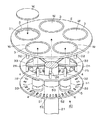
本発明の一実施形態である成膜装置1について、図1の縦断側面図、図2の平面図を各々参照しながら説明する。成膜装置1は、後述する回転テーブルに載置されて公転するウエハWに、シリコン(Si)を含む原料ガスと、酸化ガスとを順番に繰り返し供給し、これら原料ガスと酸化ガスとを互いに反応させてSiO2(酸化シリコン)膜を形成するALDが行われるように構成されている。
The
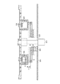
成膜装置1は、平面形状が概ね円形の扁平な処理容器である真空容器11を備えている。真空容器11は、容器の側壁及び底部をなす容器本体13と、天板12とにより構成されている。図中2は、真空容器11内に設けられた上記の回転テーブルであり、水平な円板状に形成されている。回転テーブル2の中心部には鉛直下方へ伸びる回転軸21が接続されている。この回転軸21は、容器本体13を構成する底部14に設けられた軸受け部22を貫通して、真空容器11の外側に設けられる公転用回転機構23に接続されている。公転用回転機構23によって、上面側から見て回転テーブル2は、例えば時計回りに回転される。
The
容器本体13の底部14には、回転軸21を囲むように当該底部14を厚さ方向に貫通する平面視環状のスリット24が設けられている。そして、底部14の下方には、平面視環状、且つ縦断面視凹部形状をなす空間形成部15が設けられており、この凹部内の空間は、真空容器11の外部から区画されると共に、成膜処理時には後述の排気口36、37により排気されて真空雰囲気となる。当該空間を従動ギア移動空間16とすると、この従動ギア移動空間16には、容器本体13の底部14に近接するように、水平な支持用円環板25が設けられている。また、空間形成部15の底部は円環状の水平な板により構成されており、当該板を区画板17とする。仕切り部材をなすこの区画板17は、後述する従動ギア4と駆動ギア5との間に形成される磁力線を通す材料、例えばアルミニウムやSUS(ステンレス鋼)により構成されている。区画板17の厚さH1は例えば5mm以下、より具体的には例えば3mm以下である。なお、図中18は、空間形成部15の側壁及び底部14に設けられる冷媒流路である。
The bottom 14 of the
続いて、回転テーブル2及び当該回転テーブル2に付帯する各部の構造についての概略斜視図である図3も参照しながら説明する。上記の軸受け部22の上端部からは、平面視放射状に5本のスポーク26が延出されており、当該スポーク26に回転テーブル2が支持されている。このスポーク26は、高い強度及び高い耐熱性を有するように、例えば合金であるインコネル(登録商標)により構成されている。スポーク26の先端部は、上記の容器本体13のスリット24を下方へ向かうように屈曲し、支持用円環板25の上面に接続されている。従って、支持用円環板25はスポーク26によって、回転軸21に支持されている。
Subsequently, FIG. 3 which is a schematic perspective view of the structure of the rotary table 2 and each part attached to the rotary table 2 will be described. Five
回転テーブル2の上面側(一面側)には、回転テーブル2の回転によって公転する平面視円形の載置台3が設けられている。この例では載置台3は回転テーブル2の回転方向に沿って5個設けられている。載置台3の上面には、ウエハWを水平に載置して収納するための凹部31が形成されている。
On the upper surface side (one surface side) of the rotary table 2, a mounting table 3 having a circular shape in a plan view is provided, which revolves by the rotation of the rotary table 2. In this example, five mounting tables 3 are provided along the rotation direction of the rotary table 2. A
各載置台3の下面側中央部には、載置台3を支持する自転軸32が鉛直下方へ延出するように設けられている。各自転軸32は支持用円環板25を貫通し、さらに、当該支持用円環板25の下面に支持されて設けられる5つの軸受けユニット33(図3では4つのみ表示している)を各々貫通する。自転軸32が支持用円環板25を貫通する位置は、支持用円環板25を周方向に見て隣り合うスポーク26の間である。つまり、支持用円環板25には自転軸32とスポーク26とが交互に配置されている。上記の軸受けユニット33は、自転軸32を回転自在に保持するように自転軸32を囲むベアリングと、ベアリングからのパーティクルの飛散を防ぐための磁気シールと、を備えている。このように構成されることで、自転軸32は回転テーブル2と共に回転する部位に自転自在に設けられている。また、この自転軸32は軸受けユニット33に支持されており、この軸受けユニット33は支持用円環板25、スポーク26を介して回転軸21に対して支持されている。
At the center of each mounting table 3 on the lower surface side, a
そして、自転軸32の下端部には水平な円板状の従動ギア4が、自転軸32と互いに中心軸を一致させた状態で設けられている。従って、従動ギア4は自転軸32を介して載置台3に連結されており、従動ギア4は回転テーブル2の回転により、当該回転テーブル2の回転軸21の回りを水平方向に公転する。また、従動ギア4を周方向に回転させると、各載置台3が自転軸32まわりに自転する。図1に示す従動ギア4と区画板17との距離H2は、例えば1mmである。
A horizontal disk-shaped driven
図4は従動ギア4の下面側を模式的に示している。従動ギア4の下部側には、当該従動ギア4の回転方向に沿って、多数の永久磁石が全周に亘って埋設されている。なお、ここで言う全周に亘って永久磁石が設けられるとは、回転方向に見たときに永久磁石が設けられる領域が局所的では無いことを意味している。従って、回転方向に隣り合う永久磁石間に隙間があっても、全周に亘って永久磁石が設けられることになり、この例ではそのような隙間が設けられている。
FIG. 4 schematically shows the lower surface side of the driven
従動ギア4に設けられる上記の永久磁石の磁極をN極部41、S極部42とすると、当該従動ギア4を下面側から見たときに、N極部41、S極部42が自転方向(回転方向)に沿って交互に配置されている。なお、N極部41についてはS極部42と区別するために、図中に斜線を付して表示している。この例では、従動ギア4の下面に露出するN極部41、S極部42は、夫々同じ形状の短冊状に形成され、従動ギア4の下面の中心部から横方向に放射状に延びるように、周方向に互いに間隔を開けて例えば18個配列されている。N極部41及びS極部42の長さは例えば従動ギア4の底面の中心を越えないように、従動ギア4の半径より短く設定されている。なお、高温環境下における減磁を抑制するために、上記の従動ギア4を構成する永久磁石及び後述の駆動ギア5を構成する永久磁石は、例えばサマリウムコバルト磁石により構成されている。
Assuming that the magnetic poles of the permanent magnets provided in the driven
図1及び図3に示すように、真空容器11の外側(大気雰囲気側)で、空間形成部15の下方には、駆動ギア5が配置されている。この駆動ギア5は、従動ギア4と共に磁気ギア機構40を構成する。駆動ギア5は従動ギア4の公転軌道の全周に沿って形成された水平な円環板であり、当該公転軌道に臨むように設けられている。従って駆動ギア5の上面は、従動ギア4の下面に対向する。
As shown in FIGS. 1 and 3, a
図中50は、駆動ギア5の中央部に形成された円形の開口部であり、平面で見て、当該開口部50の中心は、回転テーブル2の回転中心に一致している。また、図1に示すように駆動ギア5の下面には、駆動ギア5を回転させるための例えば環状のダイレクトドライブモータ(DDモータ)よりなる自転用回転機構53が、回転軸21を囲むように設けられており、この自転用回転機構53により、駆動ギア5が開口部50の中心を回転中心として回転する。従って、駆動ギア5は、従動ギア4の公転軌道に臨んだ状態で回転する。自転用回転機構53は回転軸を囲む平面視円環状の昇降台54に設けられており、昇降台54は、駆動ギア用昇降機構55により昇降する。図中56は駆動ギア用昇降機構55が設けられる水平な床板であり、回転軸21が貫通する開口部57を備えている。
駆動ギア5について、さらに詳しく説明する。駆動ギア5の上部には、従動ギア4の公転軌道の外周縁部に対向するように、当該駆動ギア5の全周に亘って、永久磁石が埋設されている。ここでも全周に亘って永久磁石が設けられるとは、駆動ギア5の回転方向に見たときに永久磁石が設けられる領域が局所的では無いことを意味しており、回転方向に永久磁石が隙間無く設けられることでは無い。この例では当該回転方向に隣り合う永久磁石の間に、そのような隙間が設けられている。駆動ギア5に設けられる永久磁石の磁極をN極部51及びS極部52とすると、駆動ギア5を上側から見て、駆動ギア5の回転方向にN極部51及びS極部52が交互に配置されている。なお、図3及び後述の図5などにおいては、N極部51についても、駆動ギア5のN極部41と同様に図中に斜線を付して示している。
The
図5は、1つの従動ギア4の磁極部(N極部41及びS極部42)と、その下方側の駆動ギア5の磁極部(N極部51及びS極部52)とを対応させて描いたものである。例えばN極部51、S極部52は、従動ギア4の下面に形成されたN極部41、S極部42の形状と重なり合うように短冊状に形成されている。なお、図5は、従動ギア4のN極部41と駆動ギア5のS極部52とが重なった状態を示している。また、この図5及び後述の図6、図7は磁気ギアの構成を説明するための概要図であるため、磁極部の数は実際の装置の磁極部の数と異なる。
In FIG. 5, the magnetic pole portions (
続いて、載置台3の公転と自転とについて説明する。図6は、回転テーブル2と駆動ギア5とが各々停止している状態(回転していない状態)において、5個の従動ギア4の一部が駆動ギア5と対向して停止している状態を示している。従動ギア4は、従動ギア4の各磁極部(N極部41、S極部42)と駆動ギア5の各磁極部(N極部51、S極部52)との間の吸引力及び反発力の総合作用により決定される位置において停止する。従って、回転テーブル2と駆動ギア5とを同じ回転数(回転速度:rpm)で回転させたときには、従動ギア4は駆動ギア5に対して相対的に停止していることから、従動ギア4即ち載置台3は、自転することなく停止している。
Next, the revolution and rotation of the mounting table 3 will be described. FIG. 6 shows a state in which a part of the five driven
載置台3は、駆動ギア5と回転テーブル2との回転数に差が生じたとき、即ち駆動ギア5の角速度と、回転テーブル2の回転による従動ギア4の角速度(いわば公転角速度)との間に速度差が発生したときに自転する。駆動ギア5の角速度Vaが従動ギア4の角速度Vbよりも大きいとき(駆動ギア5の角速度から従動ギア4の角速度を差し引いた速度差がプラスのとき)は、駆動ギア5に対向している従動ギア4のN極部41、S極部42の並びの下方を、駆動ギア5のN極部51、S極部52の配列が、図5で言えば左側から右側に移動していく。このため、従動ギア4に作用する駆動ギア5からの反発力と吸引力とが右側に移動し、これに伴い従動ギア4のN極部41、S極部42の並びも右に引き連れられることから、結果として従動ギア4が図5における右回転、即ち図6に示す状態から図7に示す状態のように、時計回りに自転することになる。なお、図6ではリング状の従動ギア4の公転軌道について、4Aとして示している。
The mounting table 3 is used when there is a difference in the number of rotations between the
また、駆動ギア5の角速度Vaが従動ギア4の角速度Vbよりも小さいとき(駆動ギア5の角速度から従動ギア4の角速度を差し引いた速度差がマイナスのとき)は、駆動ギア5に対向している従動ギア4のN極部41、S極部42の並びの下方を、駆動ギア5のN極部51、S極部52の配列が、図5で言えば右側から左側に移動していく。このため従動ギア4に作用する駆動ギア5からの反発力と吸引力とが左側に移動し、これに伴い従動ギア4のN極部41、S極部42の並びも左に引き連れられることから、結果として従動ギア4が図5における左回転、即ち反時計回りに自転することになる。
When the angular velocity Va of the
従動ギア4の公転による角速度と駆動ギア5の角速度との速度差と、従動ギア4の自転速度とは、図8に示すように、速度差のある範囲においてほぼ比例関係を維持する。図8中、横軸は駆動ギア5の角速度Vaと従動ギア4の公転による角速度Vbとの速度差(Va−Vb)であり、縦軸は従動ギア4の自転速度である。速度差がプラス((Va−Vb)>0)のときには、速度差がゼロから+V1までは、速度差が大きくなるほど右回りの自転速度が大きくなる。また速度差がマイナス((Va−Vb)<0)のときには、速度差がゼロから−V2までは、速度差が大きくなるほど左回りの自転速度が大きくなる。例えば駆動ギア5の角速度は、前記速度差と従動ギア4の自転速度とがほぼ比例関係を維持している値までの間において設定される。
As shown in FIG. 8, the speed difference between the angular velocity due to the revolution of the driven
このように、載置台3は、駆動ギア5と回転テーブル2との回転数に差が生じたときに自転するが、このときの自転速度は、駆動ギア5と従動ギア4とのギア比×回転速度差により求められる。回転速度差とは、駆動ギア5の角速度と、回転テーブル2の回転による従動ギア4の角速度(いわば公転角速度)との速度差である。駆動ギア5を300極の磁極部(N極部51及びS極部52)により構成し、従動ギア4を18極の磁極部(N極部41及びS極部42)により構成した場合、例えば回転テーブル2の回転数が30rpmのときに、駆動ギア5を0.1度/秒(6度/分)進める場合の自転速度は、次のように求められる。ギア比は300/18=16.67であり、回転速度差は6/360rpmであるため、従動ギア4の自転速度は、ギア比×回転速度差により、300/18×6/360=0.278rpm(100度/分)となる。
In this way, the mounting table 3 rotates when there is a difference in the number of rotations between the
上述の図8に示す従動ギア4の自転速度と、従動ギア4の公転による角速度(公転速度)と駆動ギア5の角速度との速度差と、の関係は、後述する制御部100の記憶部に記憶される。例えば成膜処理や装置のメンテナンスを行う際に、成膜装置1のユーザーは、制御部100の入力部104から従動ギア4の自転速度と、回転テーブル2の回転数とを入力することで、入力されたこれらのパラメータと、記憶部に記憶される上記の関係とに基づいて、駆動ギア5の回転数が決定され、決定された回転数で駆動ギア5を回転させることができる。
The relationship between the rotation speed of the driven
ところで相対距離変更機構である上記の駆動ギア用昇降機構55によって、図9に示すように駆動ギア5は昇降する。それにより、駆動ギア5と従動ギア4の公転軌道との離間距離H3を変更してウエハWに処理を行うことができる。この離間距離H3は例えば1mm〜5mmの範囲内で変更される。このように離間距離H3を変更可能に装置を構成する理由について説明する。上記のように従動ギア4及び駆動ギア5は永久磁石によって構成されており、この永久磁石は環境温度に応じて減磁する。従って、例えば室温付近では図7で説明したように駆動ギア5の回転によって従動ギア4が問題無く自転しても、ウエハWの処理温度が比較的高く設定されることで成膜処理中にこれら従動ギア4及び駆動ギア5の環境温度が比較的高くなる場合には、この減磁によって従動ギア4が自転しなくなるおそれが有る。また、回転テーブル2の回転数、即ち自転軸32の公転速度が高いほど、自転軸32にかかる遠心力が大きくなり、自転軸32は軸受けユニット33の内周壁をなすベアリングにおいて、回転テーブル2の外側方向に向かう部位を押圧し、当該部位への負荷が大きくなる。つまり、回転テーブル2の回転数によって、自転軸32を回転させるために必要最低限のトルクが変化する。
By the way, the
そこで、回転テーブル2の回転数が高い場合にも自転に必要なトルクが得られるように、従動ギア4と駆動ギア5との間の磁力を比較的強くするように構成することが考えられるが、従動ギア4と駆動ギア5との間に常時強力な磁力が作用すると、上記のように従動ギア4の公転軌道の周縁部側に対向するように駆動ギア5の磁極部(N極部51及びS極部52)が設けられているため、磁力の作用によって自転軸32が上記の軸受けユニット33のベアリングの回転テーブル2の外側方向に向かう部位を押圧することになり、当該部位の負荷が大きくなる。また、自転軸32及び載置台3が磁力によって下方へ強く引かれることで回転テーブル2への負荷が大きくなるし、回転軸21への負荷が大きくなってしまう。つまり、これら回転テーブル2、回転軸21及び軸受けユニット33が破損する時期が早くなるおそれが有る。そこで成膜装置1においては、上記の離間距離H3が調整されることで、駆動ギア5と従動ギア4との間の磁力が必要且つ適切なものにできるように構成されている。
Therefore, it is conceivable to configure the rotary table 2 so that the magnetic force between the driven
図1及び図2に戻って、成膜装置1の説明を続ける。図中Cは平面視円形の中心領域形成部であり、真空容器11の天板12の下面中央部に設けられる。図中34は、中心領域形成部Cから回転テーブル2の外側に向かって広がるように形成された平面視扇状の突出部であり、回転テーブル2の周方向に離れて2つ設けられている。中心領域形成部C及び突出部34は、その外側領域に比べて低い天井面を形成している。中心領域形成部Cと回転テーブル2の中心部との隙間には図示しない供給路からN2ガスが供給されることで、当該回転テーブル2の中心部における原料ガス及び酸化ガスの接触が抑制される。
Returning to FIGS. 1 and 2, the description of the
容器本体13の底部14には、ウエハWを加熱するためのヒータ35が埋設されている。底部14における回転テーブル2の外側には、排気口36、37が開口しており、真空ポンプなどにより構成される不図示の真空排気機構に接続されている。また、真空容器11の側壁面には、ゲートバルブ38により開閉自在なウエハWの搬入出部39が形成されており、当該搬入出部39を介して図示しない搬送機構により、真空容器11の内外で基板が搬送される。
A
搬入出部39付近の真空容器11の底部14には、上記のウエハWの搬送機構と載置台3との間でウエハWを受け渡すために、3本の昇降ピン20が設けられている。ただし図1では便宜上、2本のみ昇降ピン20を示している。なお、図示は省略しているが、上記の載置台3の底部には当該昇降ピン20が通過して、ウエハWの受け渡しが行えるように貫通孔が形成されている。昇降ピン20の下端は、例えば昇降及び回転する駆動ギア5に干渉しないように形成されると共に昇降機構28により昇降自在なアーム27に支持されている。図中29は昇降ピン20を囲むベローズであり、真空容器11内の気密性を保つ役割を有する。
Three elevating
回転テーブル2の上方側には、原料ガスノズル61、分離ガスノズル62、酸化ガスノズル63、改質ガスノズル64、分離ガスノズル65が、この順に、回転テーブル2の回転方向に間隔をおいて配設されている。各ガスノズル61〜65は、真空容器11の側壁から中心部に向かって、回転テーブル2の径方向に沿って水平に伸びる棒状に形成され、その長さ方向に沿って互いに間隔を開けて設けられた多数の吐出口66から、各種のガスを下方側に向けて吐出する。
On the upper side of the rotary table 2, a raw
原料ガスノズル61は原料ガスとしてBTBAS(ビスターシャルブチルアミノシラン)ガスを吐出する。図中67は、原料ガスノズル61を覆うノズルカバーであり、その下方におけるBTBASガスの濃度を高める役割を有する。酸化ガスノズル63は酸化ガスとしてO3(オゾン)ガスを吐出する。分離ガスノズル62、65はN2ガスを吐出し、上面側から見て天板12の突出部34を各々周方向に分割する位置に配置されている。改質ガスノズル64は、例えばアルゴン(Ar)ガスと酸素(O2)ガスとの混合ガスからなる改質ガスを吐出する。この例では、原料ガス、酸化ガス及び改質ガスが夫々処理ガスに相当し、原料ガスノズル61、酸化ガスノズル63及び改質ガスノズル64が、処理ガス供給部に夫々相当する。
The raw
改質ガスノズル64の上方側において、真空容器11の天板12に設けられる開口部19を塞ぐように、プラズマ形成部7が設けられている。図2には、当該プラズマ形成部7が設けられる位置を一点鎖線で示している。図中71は、石英などの誘電体からなる本体部であり、図中72は突状部であり、本体部71の下面において開口部19に沿って下方側へ向けて突出する。突条部72にて囲まれる領域内に、改質ガスノズル64から改質ガスが吐出される。本体部71の上面側には、ファラデーシールド73、絶縁用の板部材74を介して、金属線をコイル状に巻回したアンテナ75が設けられ、このアンテナ75には高周波電源76が接続されている。図中77はファラデーシールド73に設けられたスリットであり、電磁界の磁界成分を下方に向かわせる役割を有する。
A
回転テーブル2上において、原料ガスノズル61の下方領域は、BTBASガスの吸着が行われる吸着領域R1、酸化ガスノズル63の下方領域は、BTBASガスが酸化される酸化領域R2である。また、プラズマ形成部7の下方領域は、プラズマによりSiO2膜の改質が行われる改質領域R3である。突出部34の下方領域は、分離ガスノズル62、65から各々吐出されるN2ガスにより、吸着領域R1の雰囲気と酸化領域R2の雰囲気とを互いに分離するための分離領域D1、D2である。
On the rotary table 2, the lower region of the raw
既述の排気口36は、吸着領域R1と、吸着領域R1の回転方向の下流側に隣接する分離領域D1との間の外側に開口しており、余剰のBTBASガスを排気する。また、排気口37は、改質領域R3と改質領域R3の回転方向下流側に隣接する分離領域D2との境界付近の外側に開口しており、余剰のO3ガス、改質ガスを排気する。排気口36、37からは、各分離領域D1、D2、中心領域形成部Cから各々供給されるN2ガスも排気される。
The
成膜装置1には、装置全体の動作のコントロールを行うためのコンピュータからなる制御部100が設けられている。図10は、当該制御部100の概略構成を示している。この制御部100は、CPU101、後述の成膜処理に係る動作を実行するプログラム105を格納するプログラム格納部102、記憶部103、入力部104を備えている。図中110はバスである。
The
記憶部103には、回転テーブル2の回転数と、ウエハWの処理温度と、上記の駆動ギア5と従動ギア4との離間距離H3との対応関係が記憶されている。入力部104は、成膜装置1のユーザーがウエハWの処理レシピとして、成膜処理時における回転テーブル2の回転数と、ウエハWの処理温度とを各々入力して設定するためのデバイスであり、例えばタッチパネルなどにより構成される。そのように入力された回転テーブル2の回転数とウエハWの処理温度とに対応する離間距離H3が記憶部103から読み出され、そのように読み出された離間距離H3となるように駆動ギア用昇降機構55により駆動ギア5の高さが制御されて、成膜処理が行われる。
The
ウエハWの処理温度が一定である場合、回転テーブル2の回転数が高いほど既述した理由により、載置台3を自転させるために高いトルクが必要となるため、離間距離H3が小さくなるように設定される。例えば図10において、ウエハWの温度がa1℃であるときの回転テーブル2の回転数が60rpm、70rpm、80rpmである場合の離間距離H3を夫々b1mm、c1mm、d1mmとして表しているが、b1>c1>d1である。また、回転テーブル2の回転数が一定である場合には、ウエハWの温度が高いほど既述したように駆動ギア5及び従動ギア4の減磁が起こりやすいので、離間距離H3が小さくなるように設定される。例えば図10において、回転テーブル2の回転数が60rpmであり、ウエハWの温度がa1℃、a2℃、a3℃であるときの離間距離H3を夫々b1mm、c1mm、d1mmとして表しているが、a1℃<a2℃<a3℃として、b1>c1>d1である。
When the processing temperature of the wafer W is constant, the higher the rotation speed of the rotary table 2, the higher the torque required to rotate the mounting table 3 for the reason described above, so that the separation distance H3 becomes smaller. Set. For example, in FIG. 10, the separation distances H3 when the rotation speeds of the rotary table 2 are 60 rpm, 70 rpm, and 80 rpm when the temperature of the wafer W is a1 ° C. are represented as b1 mm, c1 mm, and d1 mm, respectively. c1> d1. Further, when the rotation speed of the rotary table 2 is constant, the higher the temperature of the wafer W, the more likely it is that the
上記のプログラム105は、成膜装置1の各部に制御信号を送信して各部の動作を制御し、後述の成膜処理を実行するためのステップ群が組まれている。例えば自転用回転機構53による駆動ギア5の回転数、公転用回転機構23による回転テーブル2の回転数、駆動ギア用昇降機構55による駆動ギア5の昇降、各ガスノズル61〜65からの各ガスの供給流量、ヒータ35によるウエハWの処理温度(加熱温度)、中心領域形成部CからのN2ガスの供給流量などが制御信号に従って制御される。プログラム105を格納するプログラム格納部102は、ハードディスク、コンパクトディスク、光磁気ディスク、メモリカード、DVDなどの記憶媒体により構成されており、当該記憶媒体からプログラム105は制御部100にインストールされる。
The
続いて成膜装置1による成膜処理について説明する。例えば駆動ギア5が所定の高さ位置に位置した状態で、成膜装置1のユーザーが入力部104から、回転テーブル2の回転数及びウエハWの処理温度の設定を行うと、図9、図10で説明したように、設定された回転テーブル2の回転数及びウエハWの処理温度に対応する離間距離H3となる高さ位置に、駆動ギア5が移動する。続いて、回転テーブル2の間欠的な回転と昇降ピン20の昇降動作とにより、図示しない搬送機構により外部から真空容器11内に順次搬入されるウエハWが、載置台3に受け渡される。全ての載置台3にウエハWが載置されると、ゲートバルブ38が閉じられ、真空容器11内が所定の圧力の真空雰囲気となるように排気口36、37から排気が行われる。そして、分離ガスノズル62、65、中心領域形成部Cから回転テーブル2に対してN2ガスが供給される。その一方で、ヒータ35が昇温して、ウエハWが設定された処理温度になるように加熱される。
Subsequently, the film forming process by the
そして、回転テーブル2が設定された回転数で回転すると共に、例えば駆動ギア5を回転テーブル2と等速で回転させる。これにより、載置台3は自転を停止した状態で公転する。次いで、原料ガスノズル61、酸化ガスノズル63、改質ガスノズル64からの各処理ガスの供給と、高周波電源76からのアンテナ75への高周波の印加によるプラズマの形成と、が開始される。また、駆動ギア5の回転数が、回転テーブル2の回転数と異なる回転数となるように変更され、載置台3が所定の回転数で自転する。
Then, the rotary table 2 rotates at a set rotation speed, and for example, the
図2に示すように、真空容器11内においては吸着領域R1と酸化領域R2との間に、N2ガスが供給される分離領域D1を設けているので、吸着領域R1に供給される原料ガス及び酸化領域R2に供給される酸化ガスは、回転テーブル2上で互いに混合されずに排気される。また、吸着領域R1と改質領域R3との間にもN2ガスが供給される分離領域D2を設けているので、原料ガスと、改質領域に供給される改質ガス及び改質領域R3の回転方向上流側から当該分離領域D2に向かう酸化ガスとは、回転テーブル2上で互いに混合されずに排気口36、37から排気される。また、中心領域形成部Cから供給されたN2ガスも、排気口36、37から排気される。
As shown in FIG. 2, between the oxidized region R2 and the suction region R1 in the
上述のように各ガスの供給と排気とが行われた状態で、各ウエハWは、吸着領域R1、酸化領域R2、改質領域R3を順番に通過する。吸着領域R1では原料ガスノズル61から吐出されたBTBASガスがウエハWに吸着され、酸化領域R2では吸着されたBTBASガスが、酸化ガスノズル63から供給されたO3ガスにより酸化されて、SiO2の分子層が1層あるいは複数層形成される。改質領域R3では、前記SiO2の分子層が改質ガスのプラズマに曝されて改質される。そして、回転テーブル2の回転により、上述のサイクルが複数回、繰り返し実行されることにより、SiO2の分子層が積層されてウエハWの表面にSiO2膜が形成される。図11は、このように成膜が行われるときの成膜装置1の各部の動作を示している。
With each gas supplied and exhausted as described above, each wafer W passes through the adsorption region R1, the oxidation region R2, and the reforming region R3 in this order. BTBAS gas discharged from the raw
この成膜装置1においては、回転テーブル2の回転と並行して、載置台3の回転によるウエハWの自転が行われるが、回転テーブル2の回転と載置台3の回転とが同期しないように、回転テーブル2の回転数と載置台3の自転速度が設定される。即ち、ウエハWが第1の向きに向いた状態で、回転テーブル2が回転の開始ポイントから1回転し、再度開始ポイントに位置したときに、ウエハWが第1の向きとは異なる第2の向きに向けられるような自転速度でウエハWが自転するように設定される。
In this
このように、載置台3は回転テーブル2の回転と同期せずに自転するので、各載置台3上のウエハWは自転及び公転によって、原料ガスの吸着領域R1を様々な向きで通過することになる。こうして、載置台3の自転に伴い、上面側から見た向きを次第に変えながら上述のSiO2の分子層を形成するサイクルが実行される。ウエハWの向きを変えながら成膜が行われることで、例えば吸着領域R1内で原料ガスの濃度分布にばらつきが生じている場合であっても、複数回実行されるSiO2分子層の形成サイクルの全期間で見たとき、ウエハWに吸着される原料ガスの量をウエハWの周方向に向けて揃えることができる。その結果として、ウエハWの周方向に見て、ウエハWに形成されるSiO2膜の膜厚の偏りを抑えることができる。 In this way, since the mounting table 3 rotates on its axis without synchronizing with the rotation of the rotary table 2, the wafer W on each mounting table 3 passes through the adsorption region R1 of the raw material gas in various directions by rotation and revolution. become. In this way, as the mounting table 3 rotates, the cycle of forming the molecular layer of SiO 2 described above is executed while gradually changing the orientation when viewed from the upper surface side. By forming the film while changing the orientation of the wafer W, for example, even if the concentration distribution of the raw material gas varies in the adsorption region R1, the SiO 2 molecular layer forming cycle is executed a plurality of times. When viewed over the entire period, the amount of the raw material gas adsorbed on the wafer W can be made uniform in the circumferential direction of the wafer W. As a result, it is possible to suppress the unevenness of the film thickness of the SiO 2 film formed on the wafer W when viewed in the circumferential direction of the wafer W.
上述の動作により、SiO2の分子層が順次積層され、予め設定されたサイクル数を実行したら、回転テーブル2の回転、駆動ギア5の回転、各種のガスの供給、プラズマの形成を停止し、成膜処理が終了する。然る後、ウエハWは真空容器11内への搬入時とは逆の手順で当該真空容器11内から搬出される。
By the above operation, the molecular layers of SiO 2 are sequentially laminated, and after executing a preset number of cycles, the rotation of the rotary table 2, the rotation of the
上記の成膜装置1によれば、駆動ギア用昇降機構55により、従動ギア4と駆動ギア5との離間距離H3が調整され、駆動ギア5と従動ギア4との間の磁力が調整される。従って、駆動ギア5と従動ギア4との間に強力な磁力が常時働くことを防いで回転テーブル2、回転軸21などへの各部品への負荷を抑制し、当該各部品の消耗、変形及び破損を抑制しつつ、成膜処理時に載置台3が自転するために必要な磁力を確保することができる。
According to the
上記の成膜装置1では、従動ギア4の公転に対して駆動ギア5を昇降させて上記の離間距離H3が変更されるが、駆動ギア5に対して従動ギア4を昇降させることで離間距離H3が変更されるようにしてもよい。具体的には例えば、公転用回転機構23を昇降機構に接続し、当該回転テーブル2及び真空容器11が昇降するように構成することで、そのように駆動ギア5に対して従動ギア4を昇降させることができる。
In the
また上記の例では、制御部100の記憶部103には、ウエハWの処理温度と回転テーブル2の回転数と離間距離H3との対応関係が記憶されているが、ウエハWの処理温度と離間距離H3との対応関係、回転テーブル2の回転数と離間距離H3と対応関係のいずれか一方が記憶されていてもよい。つまり、成膜装置1のユーザーがウエハWの処理温度及び回転テーブル2の回転数のうちの一方を設定することで、離間距離H3が設定されてもよい。さらに、処理レシピに応じて離間距離H3を変更することには限られない。例えば、上記の成膜処理が行われていない待機状態であるときに、上記の離間距離H3が比較的大きくなる高さ位置に駆動ギア5を位置させておき、成膜処理を行う際には、離間距離H3が比較的小さくなる予め設定された高さ位置に駆動ギア5を位置させるようにしてもよい。つまり、各成膜処理時において駆動ギア5の高さが揃う場合も本発明の権利範囲に含まれる。ただし、より確実に従動ギア4を回転させ、且つ成膜装置1の各部への負荷を抑制するためには、上記のように処理レシピに応じて駆動ギア5の高さを制御することが好ましい。
Further, in the above example, the
既述のように、成膜装置1では、ウエハWへの成膜時にこれらの公転と自転とが互いに並行して行われるが、ウエハWの自転には、回転テーブル2が回転している間、ウエハWが連続的に自転する場合の他に、間欠的に自転することも含まれる。また、ウエハWの自転の開始及び停止のタイミングは、公転の開始及び停止のタイミングと揃えるようにしてもよいし、互いの回転の開始及び停止のタイミングがずれていてもよい。また、駆動ギア5は、上記の例では大気雰囲気に設けられているが、真空容器11を駆動ギア5についても囲むように構成することで、従動ギア4と同様に真空雰囲気に設けてもよい。
As described above, in the
ところで駆動ギア5及び従動ギア4からなる磁気ギア機構40としては、磁力により駆動ギア5の回転に応じて、従動ギア4が駆動ギア5に対して非接触で回転するように構成されていればよい。従って、従動ギア4、駆動ギア5の一方だけが磁性体であってもよい。また、従動ギア4または駆動ギア5について、上記のN極部、S極部が交互に配列された構成とすることには限られず、例えばS極部、N極部の一方のみにより構成されるようにしてもよい。ただし、従動ギア4及び駆動ギア5において、各々既述の実施形態のように異なる磁極を交互に配置することで、磁石の反発力と吸引力を利用して載置台3を自転させるので、載置台3を確実に回転させることができるため好ましい。また、駆動ギア5の回転により従動ギア4を回転させることができれば、各磁極部の形状についても既述の例のように長方形状に構成することには限られない。
By the way, if the
(評価試験)
本発明に関連して行われた評価試験について説明する。評価試験1では成膜装置1と略同様の構成を備える実験装置を用いて、回転テーブル2の回転数、駆動ギア5の回転数を各々変更した場合における、回転テーブル2に載置される各ウエハWの自転速度の平均について調べた。この実験装置では、図1で説明した区画板17の厚さH1を3mm、区画板17と従動ギア4の下面との距離H2を1mm、区画板17と駆動ギア5の上面との距離を1mmに夫々設定している。従ってこの実験装置において、図9で説明した駆動ギア5と従動ギア4との公転軌道との離間距離H3は、5mmである。回転テーブル2については30rpm、60rpmまたは120rpmで回転させた。また、駆動ギア5の回転数については、回転テーブル2の回転数との差が、−0.8度/秒〜+0.8度/秒の範囲内に収まるように変更した。
(Evaluation test)
The evaluation test conducted in connection with the present invention will be described. In the
図12、図13、図14のグラフは回転テーブル2の回転数が夫々30rpm、60rpm、120rpmであるときの試験結果を示したグラフである。グラフの横軸は、駆動ギア5の回転数(単位:rpm)を示しており、グラフの縦軸は、ウエハWの平均自転速度(単位:度/分)を示している。各グラフにおいては、回転テーブル2上の5つのウエハWのうちの1つのウエハWについての結果のみを示している。これは、5つのウエハWについての平均自転速度のばらつきが略ゼロであったためである。そして各グラフに示すように回転テーブル2の回転数が30rpm、60rpm、120rpmのいずれの場合であっても、駆動ギア5の回転数の上昇に比例して、ウエハWの平均自転速度が上昇することが確認された。なお、平均自転速度が−であるときと+であるときとは、ウエハWは互いに反対の方向に自転している。
The graphs of FIGS. 12, 13 and 14 show the test results when the rotation speeds of the rotary table 2 are 30 rpm, 60 rpm and 120 rpm, respectively. The horizontal axis of the graph shows the rotation speed (unit: rpm) of the
この評価試験1の結果から、回転テーブル2の回転数が120rpm以下の範囲においては回転テーブル2によるウエハWの公転速度によらず、ウエハWの自転速度、自転の方向について制御できることが確認された。そして、区画板17によって区画されていても、駆動ギア5と従動ギア4との間に磁力が作用して従動ギア4を回転させることができることが確認された。本発明によれば、駆動ギア5が昇降し、従動ギア4と駆動ギア5との間の磁力を調整することができるので、回転テーブル2の回転数を120rpmよりも高くしても、ウエハWを所望の回転数で自転させることができることが予測される。
From the results of this
続いて評価試験2について説明する。評価試験2では、評価試験1と同様に、回転テーブル2の回転数、駆動ギア5の回転数を各々変更した場合における、回転テーブル2に載置された各ウエハWの平均自転速度について測定した。ただし、差異点として駆動ギア5と従動ギア4との公転軌道との離間距離H3(図9参照)は9mmとした。そして駆動ギア5については、設定上の各ウエハWの自転速度(自転設定速度)が+5rpm〜−5rpmになるように回転させた。回転テーブル2の回転数としては、240rpm、210rpm、180rpm、150rpm、120rpm、90rpm、60rpm、30rpm及び2rpmに設定した。
Next, the
得られた試験結果のうち、代表して回転テーブル2を240rpmさせたときの結果を図15のグラフに示す。図15のグラフの縦軸は、図12〜図14のグラフの縦軸と同様にウエハWの平均自転速度(単位:度/分)を示している。図15のグラフの横軸は、上記のウエハWの自転設定速度について示している。この図15のグラフでは、評価試験1の結果と同様に回転テーブル2上の5つのウエハWの平均自転速度のばらつきが略ゼロであったためであったため、1つのウエハWについての結果のみを示している。この図15のグラフから明らかなように、ウエハWの平均自転速度は自転設定速度に応じて+180度/分〜−180度/分の範囲内の値となり、自転設定速度の上昇に比例して、当該ウエハWの平均自転速度が上昇する。
Among the obtained test results, the results when the rotary table 2 is rotated at 240 rpm as a representative are shown in the graph of FIG. The vertical axis of the graph of FIG. 15 shows the average rotation speed (unit: degrees / minute) of the wafer W as in the vertical axis of the graphs of FIGS. 12 to 14. The horizontal axis of the graph of FIG. 15 shows the rotation setting speed of the wafer W. In the graph of FIG. 15, the variation in the average rotation speed of the five wafers W on the rotary table 2 was substantially zero as in the result of the
図示は省略するが、この評価試験2において回転テーブル2の回転数を240rpm以外の値に設定した場合のグラフの波形については、回転テーブル2の回転数を240rpmに設定した場合のグラフの波形と略同様であった。つまり、自転設定速度が変化するとウエハWの平均自転速度については、その自転設定速度が得られるように+180度/分〜−180度/分の範囲内で変化し、自転設定速度の上昇に比例して、ウエハWの平均自転速度が上昇する結果となった。そして、回転テーブル2上の5つのウエハWの平均自転速度のばらつきについても、回転テーブル2の回転数を240rpmと設定したときと同様に、略ゼロであった。
Although not shown, the waveform of the graph when the rotation speed of the rotary table 2 is set to a value other than 240 rpm in this
従って、この評価試験2の結果から、回転テーブル2の回転数が240rpm以下の範囲において、ウエハW間で自転速度が揃えられ、ウエハWの自転速度及び自転の方向について制御できることが確認された。つまり、回転テーブル2の回転数をこのような範囲に設定して、上記の成膜装置1を運用することができることが確認された。さらに、ウエハWの自転速度を+5rpm〜−5rpmとすることができることが確認された。
Therefore, from the results of this
W ウエハ
1 成膜装置
11 真空容器
2 回転テーブル
3 載置台
35 ヒータ
4 従動ギア
5 駆動ギア
55 駆動ギア用昇降機構
61 原料ガスノズル
63 酸化ガスノズル
Claims (7)
前記回転テーブルの一面側に基板を載置するために設けられ、当該回転テーブルの回転により公転する載置台と、
前記載置台に載置された前記基板を加熱する加熱部と、
前記回転テーブルの回転により載置台が通過する領域に成膜ガスを供給して前記基板に成膜する成膜ガス供給部と、
前記回転テーブルと共に回転する部位に前記載置台を支持するように自転自在に設けられる自転軸と、
前記自転軸に設けられた従動ギアと、
前記従動ギアの公転軌道に臨んで回転し、かつ前記公転軌道の全周に沿って設けられ、前記従動ギアと磁気ギア機構を構成する駆動ギアと、
横方向における前記従動ギアの公転軌道に対して、前記駆動ギアを昇降させる昇降機構であり、前記従動ギアの公転軌道と前記駆動ギアとの相対距離を変更するための相対距離変更機構と、
を備えることを特徴とする成膜装置。 A rotary table provided in the processing container and
A mounting table provided for mounting a substrate on one side of the rotary table and revolving due to the rotation of the rotary table.
A heating unit that heats the substrate placed on the above-mentioned stand, and
A film-forming gas supply unit that supplies a film-forming gas to a region through which the mounting table passes by rotation of the rotary table to form a film on the substrate, and a film-forming gas supply unit.
A rotation shaft that is rotatably provided so as to support the above-mentioned stand at a portion that rotates together with the rotary table, and
The driven gear provided on the rotation axis and
A drive gear that rotates toward the revolution orbit of the driven gear and is provided along the entire circumference of the revolution orbit and constitutes the driven gear and the magnetic gear mechanism.
An elevating mechanism that raises and lowers the drive gear with respect to the orbit of the driven gear in the lateral direction, and a relative distance changing mechanism for changing the relative distance between the orbit of the driven gear and the drive gear.
A film forming apparatus comprising.
前記回転テーブルの一面側に基板を載置するために設けられ、当該回転テーブルの回転により公転する載置台と、
前記載置台に載置された前記基板を加熱する加熱部と、
前記回転テーブルの回転により載置台が通過する領域に成膜ガスを供給して前記基板に成膜する成膜ガス供給部と、
前記回転テーブルと共に回転する部位に前記載置台を支持するように自転自在に設けられる自転軸と、
前記自転軸に設けられた従動ギアと、
前記従動ギアの公転軌道に臨んで回転し、かつ前記公転軌道の全周に沿って設けられ、前記従動ギアと磁気ギア機構を構成する駆動ギアと、
前記従動ギアの公転軌道と前記駆動ギアとの相対距離を変更するための相対距離変更機構と、
を備え、
前記処理容器内は、真空雰囲気となるように構成され、
前記駆動ギアは、大気雰囲気側に設けられ、
前記従動ギアと駆動ギアとの間には、大気雰囲気と真空雰囲気とを仕切り、磁力線を通す材料により構成された仕切り部材が設けられていることを特徴とする成膜装置。 A rotary table provided in the processing container and
A mounting table provided for mounting a substrate on one side of the rotary table and revolving due to the rotation of the rotary table.
A heating unit that heats the substrate placed on the above-mentioned stand, and
A film-forming gas supply unit that supplies a film-forming gas to a region through which the mounting table passes by rotation of the rotary table to form a film on the substrate, and a film-forming gas supply unit.
A rotation shaft that is rotatably provided so as to support the above-mentioned stand at a portion that rotates together with the rotary table, and
The driven gear provided on the rotation axis and
A drive gear that rotates toward the revolution orbit of the driven gear and is provided along the entire circumference of the revolution orbit and constitutes the driven gear and the magnetic gear mechanism.
A relative distance changing mechanism for changing the relative distance between the orbit of the driven gear and the driving gear, and
Equipped with a,
The inside of the processing container is configured to have a vacuum atmosphere.
The drive gear is provided on the atmospheric atmosphere side.
A film forming apparatus characterized in that a partition member made of a material that partitions an atmospheric atmosphere and a vacuum atmosphere and allows magnetic lines to pass through is provided between the driven gear and the drive gear.
前記駆動ギアは、前記公転軌道に沿って全周に亘ってN極部及びS極部が交互に配列されていることを特徴とする請求項1または2記載の成膜装置。 In the driven gear, the north pole and the south pole are alternately arranged along the entire circumference along the rotation direction.
The film forming apparatus according to claim 1 or 2, wherein the drive gear has N-pole portions and S-pole portions alternately arranged along the entire circumference along the revolution orbit.
前記駆動ギアの各磁極部は、前記従動ギアの下面と対向する面に配列されていることを特徴とする請求項1ないし4のいずれか一つに記載の成膜装置。 Each magnetic pole portion of the driven gear is provided on the lower surface so as to extend radially laterally from the central portion.
The film forming apparatus according to any one of claims 1 to 4, wherein each magnetic pole portion of the drive gear is arranged on a surface facing the lower surface of the driven gear.
Priority Applications (4)
| Application Number | Priority Date | Filing Date | Title |
|---|---|---|---|
| JP2017244303A JP6935741B2 (en) | 2017-12-20 | 2017-12-20 | Film deposition equipment |
| KR1020180163726A KR102458483B1 (en) | 2017-12-20 | 2018-12-18 | Film formation apparatus |
| US16/225,788 US11136669B2 (en) | 2017-12-20 | 2018-12-19 | Film formation apparatus |
| CN201811563931.7A CN109943828B (en) | 2017-12-20 | 2018-12-20 | Film forming apparatus |
Applications Claiming Priority (1)
| Application Number | Priority Date | Filing Date | Title |
|---|---|---|---|
| JP2017244303A JP6935741B2 (en) | 2017-12-20 | 2017-12-20 | Film deposition equipment |
Publications (3)
| Publication Number | Publication Date |
|---|---|
| JP2019110281A JP2019110281A (en) | 2019-07-04 |
| JP2019110281A5 JP2019110281A5 (en) | 2020-07-30 |
| JP6935741B2 true JP6935741B2 (en) | 2021-09-15 |
Family
ID=66814233
Family Applications (1)
| Application Number | Title | Priority Date | Filing Date |
|---|---|---|---|
| JP2017244303A Active JP6935741B2 (en) | 2017-12-20 | 2017-12-20 | Film deposition equipment |
Country Status (4)
| Country | Link |
|---|---|
| US (1) | US11136669B2 (en) |
| JP (1) | JP6935741B2 (en) |
| KR (1) | KR102458483B1 (en) |
| CN (1) | CN109943828B (en) |
Families Citing this family (4)
| Publication number | Priority date | Publication date | Assignee | Title |
|---|---|---|---|---|
| JP6777055B2 (en) * | 2017-01-11 | 2020-10-28 | 東京エレクトロン株式会社 | Board processing equipment |
| JP7080152B2 (en) * | 2018-10-11 | 2022-06-03 | 東京エレクトロン株式会社 | Rotation angle detection device and rotation angle detection method, and substrate processing device and substrate processing method using these. |
| JP7382836B2 (en) | 2020-01-15 | 2023-11-17 | 東京エレクトロン株式会社 | Substrate processing equipment and rotational drive method |
| CN112251730A (en) * | 2020-12-04 | 2021-01-22 | 光驰科技(上海)有限公司 | Non-contact revolution and rotation rotating frame system for vacuum coating |
Family Cites Families (9)
| Publication number | Priority date | Publication date | Assignee | Title |
|---|---|---|---|---|
| JP4605853B2 (en) * | 2000-04-20 | 2011-01-05 | 東京エレクトロン株式会社 | Heat treatment apparatus, heat treatment system, and heat treatment method |
| WO2007069433A1 (en) * | 2005-12-16 | 2007-06-21 | Niigata University | Noncontact rotating processor |
| JP6017817B2 (en) * | 2011-12-15 | 2016-11-02 | 住友化学株式会社 | Surface treatment apparatus, surface treatment method, substrate support mechanism, and program |
| JP6330623B2 (en) * | 2014-10-31 | 2018-05-30 | 東京エレクトロン株式会社 | Film forming apparatus, film forming method, and storage medium |
| JP6330630B2 (en) * | 2014-11-13 | 2018-05-30 | 東京エレクトロン株式会社 | Deposition equipment |
| JP6581831B2 (en) * | 2015-07-28 | 2019-09-25 | 東京エレクトロン株式会社 | Holding section posture maintenance mechanism |
| JP2017054880A (en) * | 2015-09-08 | 2017-03-16 | 東京エレクトロン株式会社 | Substrate processing apparatus and substrate processing method |
| JP6740881B2 (en) * | 2016-02-02 | 2020-08-19 | 東京エレクトロン株式会社 | Substrate processing equipment |
| CN107022754B (en) * | 2016-02-02 | 2020-06-02 | 东京毅力科创株式会社 | Substrate processing apparatus |
-
2017
- 2017-12-20 JP JP2017244303A patent/JP6935741B2/en active Active
-
2018
- 2018-12-18 KR KR1020180163726A patent/KR102458483B1/en active IP Right Grant
- 2018-12-19 US US16/225,788 patent/US11136669B2/en active Active
- 2018-12-20 CN CN201811563931.7A patent/CN109943828B/en active Active
Also Published As
| Publication number | Publication date |
|---|---|
| KR102458483B1 (en) | 2022-10-26 |
| CN109943828A (en) | 2019-06-28 |
| US11136669B2 (en) | 2021-10-05 |
| CN109943828B (en) | 2022-01-07 |
| US20190186004A1 (en) | 2019-06-20 |
| JP2019110281A (en) | 2019-07-04 |
| KR20190074984A (en) | 2019-06-28 |
Similar Documents
| Publication | Publication Date | Title |
|---|---|---|
| TWI694516B (en) | Substrate processing device | |
| US10584416B2 (en) | Substrate processing apparatus | |
| JP6922408B2 (en) | Board processing equipment | |
| JP6330623B2 (en) | Film forming apparatus, film forming method, and storage medium | |
| JP6935741B2 (en) | Film deposition equipment | |
| US10683573B2 (en) | Film forming apparatus | |
| CN106505014B (en) | Substrate processing apparatus and substrate processing method | |
| TWI695907B (en) | Substrate processing apparatus | |
| JP2018026528A (en) | Deposition device, deposition method and storage medium | |
| US11702746B2 (en) | Magnetic drive apparatus and magnetizing method | |
| JP2021125652A (en) | Substrate holding mechanism and substrate processing apparatus |
Legal Events
| Date | Code | Title | Description |
|---|---|---|---|
| RD02 | Notification of acceptance of power of attorney |
Free format text: JAPANESE INTERMEDIATE CODE: A7422 Effective date: 20181029 |
|
| A521 | Request for written amendment filed |
Free format text: JAPANESE INTERMEDIATE CODE: A523 Effective date: 20200615 |
|
| A621 | Written request for application examination |
Free format text: JAPANESE INTERMEDIATE CODE: A621 Effective date: 20200615 |
|
| A977 | Report on retrieval |
Free format text: JAPANESE INTERMEDIATE CODE: A971007 Effective date: 20210519 |
|
| A131 | Notification of reasons for refusal |
Free format text: JAPANESE INTERMEDIATE CODE: A131 Effective date: 20210525 |
|
| A521 | Request for written amendment filed |
Free format text: JAPANESE INTERMEDIATE CODE: A523 Effective date: 20210705 |
|
| TRDD | Decision of grant or rejection written | ||
| A01 | Written decision to grant a patent or to grant a registration (utility model) |
Free format text: JAPANESE INTERMEDIATE CODE: A01 Effective date: 20210727 |
|
| A61 | First payment of annual fees (during grant procedure) |
Free format text: JAPANESE INTERMEDIATE CODE: A61 Effective date: 20210809 |
|
| R150 | Certificate of patent or registration of utility model |
Ref document number: 6935741 Country of ref document: JP Free format text: JAPANESE INTERMEDIATE CODE: R150 |
|
| R250 | Receipt of annual fees |
Free format text: JAPANESE INTERMEDIATE CODE: R250 |