JP6934331B2 - Luminous drive circuit, vehicle lighting equipment - Google Patents
Luminous drive circuit, vehicle lighting equipment Download PDFInfo
- Publication number
- JP6934331B2 JP6934331B2 JP2017117849A JP2017117849A JP6934331B2 JP 6934331 B2 JP6934331 B2 JP 6934331B2 JP 2017117849 A JP2017117849 A JP 2017117849A JP 2017117849 A JP2017117849 A JP 2017117849A JP 6934331 B2 JP6934331 B2 JP 6934331B2
- Authority
- JP
- Japan
- Prior art keywords
- light emitting
- current
- value
- unit
- emitting elements
- Prior art date
- Legal status (The legal status is an assumption and is not a legal conclusion. Google has not performed a legal analysis and makes no representation as to the accuracy of the status listed.)
- Active
Links
Images


Classifications
-
- H—ELECTRICITY
- H05—ELECTRIC TECHNIQUES NOT OTHERWISE PROVIDED FOR
- H05B—ELECTRIC HEATING; ELECTRIC LIGHT SOURCES NOT OTHERWISE PROVIDED FOR; CIRCUIT ARRANGEMENTS FOR ELECTRIC LIGHT SOURCES, IN GENERAL
- H05B45/00—Circuit arrangements for operating light-emitting diodes [LED]
Description
本発明は、車載バッテリからの電力供給に応じて複数の発光素子を有する発光部において前記発光素子が順に発光状態に遷移していく車両用灯具における発光駆動回路と、上記車両用灯具とに関する。 The present invention relates to a light emitting drive circuit in a vehicle lighting device in which the light emitting elements sequentially transition to a light emitting state in a light emitting unit having a plurality of light emitting elements according to power supply from an in-vehicle battery, and the vehicle lighting device.
車両用灯具としては、方向指示器として用いられるターンシグナルランプの機能を有するものがある。ターンシグナルランプは、運転者等によるウィンカーレバーやハザードスイッチ等の操作に応じて、例えばメータECU(Electronic Control Unit)などの所定の車載ECUによりON/OFF制御される。 Some vehicle lighting fixtures have the function of a turn signal lamp used as a turn signal. The turn signal lamp is ON / OFF controlled by a predetermined in-vehicle ECU such as a meter ECU (Electronic Control Unit) in response to an operation of a blinker lever, a hazard switch, or the like by a driver or the like.
ECUは、車両に設けられた個々のターンシグナルランプについて個別に断線の有無を判定する機能を有している(断線検知機能)。断線有無の判定は、ターンシグナルランプへの供給電流値(ランプ側にとっては入力電流値)が所定の閾値以下となったか否かを判別することで行われる。 The ECU has a function of individually determining the presence or absence of disconnection of each turn signal lamp provided in the vehicle (disconnection detection function). The presence or absence of disconnection is determined by determining whether or not the supply current value to the turn signal lamp (input current value for the lamp side) is equal to or less than a predetermined threshold value.
近年、ターンシグナルランプとしては、発光部にLED(発光ダイオード)等の発光素子を用いたものがあり、また、発光態様として、発光部が有する複数の発光素子を所定個ずつ順に発光状態に遷移させていく態様を採用した、いわゆるシーケンシャルターンランプと呼ばれるタイプも存在する(例えば下記特許文献1を参照)。
In recent years, as a turn signal lamp, there is one that uses a light emitting element such as an LED (light emitting diode) in the light emitting part, and as a light emitting mode, a plurality of light emitting elements possessed by the light emitting part are sequentially changed to a light emitting state one by one. There is also a type called a so-called sequential turn lamp that adopts the mode of making the lamp (see, for example,
シーケンシャルターンランプにおいては、発光素子が順にON状態に遷移していくため、時間経過と共に発光部の消費電力が変動する。具体的に、発光中の発光素子数が最も少ない発光初期段階では発光部の消費電力が最も低く、全ての発光素子が発光状態となる発光終盤段階では発光部の消費電力が最も高くなる。 In the sequential turn lamp, since the light emitting elements sequentially transition to the ON state, the power consumption of the light emitting unit fluctuates with the passage of time. Specifically, the power consumption of the light emitting unit is the lowest in the initial stage of light emission when the number of light emitting elements during light emission is the smallest, and the power consumption of the light emitting unit is the highest in the final stage of light emission when all the light emitting elements are in the light emitting state.
シーケンシャルターンランプのように発光部の発光素子が順に発光状態に遷移していく車両用灯具においては、上記のように発光部の消費電力が時間経過に応じて変化するため、車載ECU側で断線検知を行う際の閾値(断線閾値)の設定が困難となる。特に、発光部における消費電力の変動幅が大きい場合(発光初期段階と発光終盤段階とで発光中素子数の差が大きい場合)には、どのような断線閾値を設定しても適切な断線検知を行うことができない虞もある。 In vehicle lamps such as sequential turn lamps, in which the light emitting elements of the light emitting part sequentially transition to the light emitting state, the power consumption of the light emitting part changes with the passage of time as described above, so that the in-vehicle ECU is disconnected. It becomes difficult to set a threshold (disconnection threshold) when performing detection. In particular, when the fluctuation range of power consumption in the light emitting part is large (when the difference in the number of elements during light emission is large between the initial stage of light emission and the final stage of light emission), appropriate disconnection detection is performed regardless of the disconnection threshold value. May not be possible.
また、シーケンシャルターンランプのような車両用灯具は、メーカ純正品としてではなく汎用品として販売されることもある。特に、トラック等の大型車両のリアコンビネーションランプとして販売される場合には、特定メーカの車両に対応した商品として販売されるのではなく、異メーカの車両にそれぞれ取り付け可能な汎用品として販売される場合がある。この際、車両メーカが異なると、ECUに設定される断線閾値も異なる場合があり、上記のような発光部の消費電力変動に対して或るメーカの車両では断線検知を適正に行うことができるが、他メーカの車両では適切な断線検知を行うことができないというケースも生じ得る。 In addition, vehicle lighting fixtures such as sequential turn lamps may be sold as general-purpose products rather than as genuine manufacturer products. In particular, when it is sold as a rear combination lamp for a large vehicle such as a truck, it is not sold as a product corresponding to a vehicle of a specific manufacturer, but as a general-purpose product that can be attached to a vehicle of a different manufacturer. In some cases. At this time, if the vehicle manufacturer is different, the disconnection threshold value set in the ECU may also be different, and the vehicle of a certain manufacturer can properly detect the disconnection against the above-mentioned fluctuation in the power consumption of the light emitting unit. However, there may be a case where the vehicle of another manufacturer cannot properly detect the disconnection.
そこで、本発明は、車載バッテリからの電力供給に応じて発光部における発光素子が順に発光状態に遷移していく車両用灯具について、発光素子の断線検知の正確性向上を図ることを目的とする。 Therefore, an object of the present invention is to improve the accuracy of wire breakage detection of a light emitting element in a vehicle lamp in which the light emitting element in the light emitting unit sequentially transitions to a light emitting state according to the power supply from the in-vehicle battery. ..
本発明に係る発光駆動回路は、車載バッテリからの電力供給に応じて複数の発光素子を有する発光部において前記発光素子が順に発光状態に遷移していく車両用灯具における発光駆動回路であって、前記車載バッテリからの電力供給ラインを介して供給される電流を受け、前記発光部におけるそれぞれの前記発光素子に駆動電流を供給する電流供給部と、前記電力供給ラインより供給される電力の一部を消費して調整電流を流す電流消費部と、前記発光部における発光中の前記発光素子の数が多いほど前記調整電流の電流値を低くする電流制御部と、を備えるものである。 The light emitting drive circuit according to the present invention is a light emitting drive circuit in a vehicle lighting tool in which the light emitting elements sequentially transition to a light emitting state in a light emitting unit having a plurality of light emitting elements according to power supply from an in-vehicle battery. A current supply unit that receives a current supplied through the power supply line from the vehicle-mounted battery and supplies a drive current to each of the light emitting elements in the light emitting unit, and a part of the power supplied from the power supply line. It is provided with a current consuming unit that consumes the current and causes the adjustment current to flow, and a current control unit that lowers the current value of the adjustment current as the number of the light emitting elements during light emission in the light emitting unit increases.
これにより、発光中素子数が少ない、つまり発光部の消費電力が小さいほど、調整電流の電流値を高くする制御が実現される。 As a result, control is realized in which the current value of the adjustment current is increased as the number of elements during light emission is small, that is, the power consumption of the light emitting unit is small.
上記した本発明に係る発光駆動回路においては、前記電流制御部は、発光中の前記発光素子の数と前記電力供給ラインからの入力電圧の電圧値とに基づいて前記調整電流の電流値を制御することが望ましい。
入力電圧が低下すると入力電流値が低下し断検閾値以下に低下する虞がある。上記構成によれば、入力電圧の電圧値に基づいて調整電流の値が制御される、つまり電流消費部による電力消費量が制御されるため、入力電圧の低下に起因して入力電流値が断検閾値以下に低下してしまうことの防止を図ることが可能とされる。
In the light emitting drive circuit according to the present invention described above, the current control unit controls the current value of the adjusted current based on the number of the light emitting elements during light emission and the voltage value of the input voltage from the power supply line. It is desirable to do.
When the input voltage drops, the input current value drops and may drop below the cutoff threshold. According to the above configuration, the value of the adjustment current is controlled based on the voltage value of the input voltage, that is, the power consumption by the current consuming unit is controlled, so that the input current value is cut off due to the decrease in the input voltage. It is possible to prevent the voltage from dropping below the inspection threshold.
上記した本発明に係る光源駆動回路においては、前記電流制御部は、前記入力電圧の電圧値が低いほど前記調整電流の電流値を低くすることが望ましい。
これにより、入力電圧の低下に応じて入力電流値が低下する場合に対応して、電力消費部による電力消費量が抑えられる。
In the light source drive circuit according to the present invention described above, it is desirable that the current control unit lowers the current value of the adjustment current as the voltage value of the input voltage decreases.
As a result, the power consumption by the power consuming unit can be suppressed in response to the case where the input current value decreases as the input voltage decreases.
上記した本発明に係る発光駆動回路においては、前記電流制御部は、前記電力供給ラインを流れる入力電流の電流値が前記発光部における発光中の前記発光素子の数に拘わらず一定となるように前記調整電流の電流値を制御することが望ましい。
これにより、入力電流値が断検閾値を上回る一定値で維持されるようにすることが可能とされる。
In the light emitting drive circuit according to the present invention described above, in the current control unit, the current value of the input current flowing through the power supply line is constant regardless of the number of the light emitting elements during light emission in the light emitting unit. It is desirable to control the current value of the adjustment current.
This makes it possible to maintain the input current value at a constant value exceeding the cutoff threshold value.
また、本発明に係る車両用灯具は、上記した本発明に係る光源駆動回路と前記発光部とを備えたものである。 Further, the vehicle lamp according to the present invention includes the light source drive circuit according to the present invention and the light emitting unit.
この車両用灯具によっても、上記した本発明に係る発光駆動回路と同様の作用が得られる。 This vehicle lamp also has the same effect as the light emitting drive circuit according to the present invention described above.
本発明によれば、車載バッテリからの電力供給に応じて発光部における発光素子が順に発光状態に遷移していく車両用灯具について、発光素子の断線検知の正確性向上を図ることができる。 According to the present invention, it is possible to improve the accuracy of wire breakage detection of a light emitting element in a vehicle lamp in which the light emitting element in the light emitting unit sequentially transitions to a light emitting state according to the power supply from the in-vehicle battery.
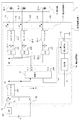
以下、本発明に係る実施形態としての発光駆動回路3を備えた車両用灯具1について添付図面を参照しながら説明する。
先ず、車両用灯具1の内部回路構成について図1のブロック図を参照して説明する。
車両用灯具1は、車両の後端部において左右一対が設けられるリアコンビネーションランプとして構成され、少なくともストップランプとターンシグナルランプとしての機能を有する。図1では、ストップランプとしての機能を実現するための構成については省略し、ターンシグナルランプとしての機能を実現するための構成について説明する。なお、以下「ターンシグナルランプ」は「ターンランプ」と略称することもある。
Hereinafter, a
First, the internal circuit configuration of the
The
車両用灯具1には、ターンランプの光源として機能する複数の発光素子20を有する発光部2と、車両における車両用灯具1外部に設けられた車載バッテリBtからの電力供給に応じて発光素子20を発光駆動する発光駆動回路3とを有している。
The
車両には、車両用灯具1に対する電力供給を制御するECU(Electronic Control Unit)100が設けられている。
ECU100は、車載バッテリBtからの出力電圧(以下「バッテリ電圧」とも表記:本例ではDC24V程度)を入力し、図示は省略したウィンカーレバーやハザードスイッチ等の操作に応じて、車両用灯具1に対するバッテリ電圧の供給を所定の周期でON/OFF(例えばON=350ms程度、OFF=350ms程度)し、これによりターンランプの点灯制御(点滅制御)を行う。この場合、ターンランプは毎分85点滅程度の周期で点滅を繰り返すことになる。
The vehicle is provided with an ECU (Electronic Control Unit) 100 that controls the power supply to the
The
車両用灯具1において、発光駆動回路3は、ECU100を介して車載バッテリBTの正極側に接続された端子T1と、車載バッテリBTの負極側に接続された端子T2とを有しており、ECU100により車両用灯具1へのバッテリ電圧の供給がONされたときには、端子T1、T2間に入力電圧Vinが発生する。またこのとき、端子T1を介して車載バッテリBTからの電力供給が行われる電力供給ラインLsには、入力電流Iinが流れる。
In the
ECU100は、バッテリ電圧の供給がONとされた期間において入力電流Iinの電流値を検出し、検出した電流値が所定の閾値THを下回っているか否かを判別することで、発光部2における発光素子20の断線有無を判定する。
この際、ECU100は、断線ありと判定した場合には、車両用灯具1に対するバッテリ電圧のON/OFF周期(つまり入力電圧VinのON/OFF周期)を通常時(非断線時)よりも短くする。例えば、上記例のように通常時が毎分85点滅程度の周期である場合、毎分110点滅程度の周期となるようにON/OFF周期を変更する。
The
At this time, when the
車両用灯具1において、発光部2には、例えばLED(発光ダイオード)によるn個(nは2以上の自然数)の発光素子20−1、20−2、…、20−nが設けられている。本例では、発光素子20の数は3以上であり、例えば5であるとする。
In the
発光駆動回路3は、入力電圧Vinに生じるコモンモードノイズの除去等を行う入力フィルタ31と、電力供給ラインLsを介して供給される電流を受け発光部2におけるそれぞれの発光素子20に駆動電流Idを供給する電流供給部32と、電流供給部32を制御して発光部2における発光素子20の発光タイミング制御を行う制御部33と、電力供給ラインLsより供給される電力の一部を消費して調整電流Imを流す電流消費部34とを備えている。
図示のように電流供給部32と電流消費部38は、入力フィルタ31の出力に対して互いが並列の関係に接続されている。
The light emitting drive circuit 3 receives a current supplied via the
As shown in the figure, the current supply unit 32 and the
電流供給部32は、n個のレギュレータIC(Integrated Circuit)35(35−1、35−2、…、35−n)と、n個の出力フィルタ36(36−1、36−2、…、36−n)とを有している。
各レギュレータIC35は、入力フィルタ31の出力に対して並列に接続され、入力電圧Vinに基づき一定電流値による電流を出力する。各レギュレータIC35は、制御部33が出力する発光制御信号St−1、St−2、…、St−nのうち対応する一つの発光制御信号StによりON/OFFされる。レギュレータIC35がONの期間には、該レギュレータIC35の正極側出力ラインと負極側出力ラインとの間に出力電圧Voが生じる(図中、出力電圧Vo−1、Vo−2、…、Vo−n)。
The current supply unit 32 includes n regulator ICs (Integrated Circuits) 35 (35-1, 35-2, ..., 35-n) and n output filters 36 (36-1, 36-2, ..., 35-n). It has 36-n).
Each
出力フィルタ36−1、36−2、…、36−nは、レギュレータIC35−1、35−2、…、35−nのうち末尾の数値が一致するレギュレータIC35の出力側に接続され、対応する出力電圧Voについてノイズ(高周波成分)の除去を行う。 The output filters 36-1, 36-2, ..., 36-n are connected to the output side of the regulator IC35 having the same last numerical value among the regulator IC35-1, 35-2, ..., 35-n, and correspond to each other. Noise (high frequency component) is removed from the output voltage Vo.
発光駆動回路3には、出力フィルタ36−1、36−2、…、36−nの正極側出力ラインと接続された端子t11、t12、…、t1nと、出力フィルタ36−1、36−2、…、36−nの負極側出力ラインと接続された端子t21、t22、…、t2nとを有しており、端子t11、t12、…、t1nはLEDによる発光素子20−1、20−2、…、20−nのうち末尾の数値が一致する発光素子20のアノードと接続され、端子t21、t22、…、t2nは発光素子20−1、20−2、…、20−nのうち末尾の数値が一致する発光素子20のカソードと接続されている。
これにより、出力電圧Vo−1、Vo−2、…、Vo−nは、それぞれ末尾の数値が一致する発光素子20に印加され、該発光素子20が発光する。図中では、このように発光される発光素子20に流れる駆動電流Idをそれぞれ末尾の数値を一致させて表している(図中、駆動電流Id−1、Id−2、…、Id−n)。
このとき、各駆動電流Idの電流値は、対応するレギュレータIC35が有する電流値調整機能により一定に調整される。
The light emitting drive circuit 3 includes terminals t11, t12, ..., T1n connected to the positive electrode side output lines of the output filters 36-1, 36-2, ..., 36-n, and output filters 36-1, 36-2. , ..., Has terminals t21, t22, ..., T2n connected to the negative electrode side output line of 36-n, and terminals t11, t12, ..., T1n are LED light emitting elements 20-1, 20-2. , ..., 20-n are connected to the anode of the
As a result, the output voltages Vo-1, Vo-2, ..., And Von are applied to the
At this time, the current value of each drive current Id is constantly adjusted by the current value adjusting function of the
制御部33は、例えばCPU(Central Processing Unit)、ROM(Read Only Memory)、RAM(Random Access Memory)等を備えたマイクロコンピュータを有して構成され、発光制御信号St−1、St−2、…、St−nによってレギュレータIC35−1、35−2、…、35−nをON/OFF制御することで、発光部2における発光素子20を順に発光状態に遷移させていく。
具体的に、制御部33は、例えば入力電圧VinがONに転じたことに応じて、発光制御信号St−1によりレギュレータIC35−1をONさせ、発光素子20−1の発光を開始させる。そして、以降は所定時間の経過ごとに、発光制御信号St−2、…、St−nによってレギュレータIC35−2、…、35−nを順にONさせていき、発光素子20−2、…、20−nの発光を順に開始させていく。
これにより、いわゆるシーケンシャルターンランプとしての発光態様、すなわち車載バッテリBtからの電力供給に応じて発光部2における発光素子20が順に発光状態に遷移していく発光態様が実現される。
なお、周知のようにシーケンシャルターンランプにおいては、入力電圧VinがONの期間において一度発光状態に遷移した発光素子20は、少なくとも最後の発光素子20が発光状態に遷移するまでの間発光状態を維持し続ける。具体的に、本例では、最後の発光素子20−nが発光状態に遷移した後に、発光素子20−1〜20−nが一斉に非発光状態に遷移する。このため制御部33は、当該一斉の非発光状態遷移タイミングまで、各レギュレータIC35のON状態を維持させる。この際、当該一斉の非発光状態遷移タイミングは、入力電圧VinがOFFに転じるタイミングと一致させることができる。その場合、入力電圧VinがOFFされることで各レギュレータIC35がOFFとされ、各発光素子20が一斉に非発光状態に遷移される。
The
Specifically, the
As a result, a light emitting mode as a so-called sequential turn lamp, that is, a light emitting mode in which the
As is well known, in the sequential turn lamp, the
また、制御部33は、電流消費部34における後述する電流調整部38を制御することで、調整電流Imの電流値を調整するが、これについては改めて説明する。
Further, the
ここで、シーケンシャルターンランプにおいては、入力電圧VinがONに転じたタイミングを基準として、発光中の発光素子20(以下「発光中素子」とも表記する)の数を増加させるタイミングが複数設定されている。具体的に本例では、発光素子20−1、20−2、…、20−nを順に発光状態に遷移させるための五つのタイミングが設定されている。以下、このように発光中素子の数を増加させるタイミングを「素子数増加タイミング」と表記する。
上記では、各素子数増加タイミングにおいて、発光中素子数を1ずつ増加させる例を挙げたが、もちろん、2以上ずつ増加させることもできる。具体的な構成としては、各レギュレータIC35に対してそれぞれ複数の発光素子20を接続する構成である。
また、上記では、各素子数増加タイミングにおいて発光中素子を同数ずつ増加させる例を挙げたが、一部又は全部の素子数増加タイミングにおいて、発光中素子の増加数を異ならせてもよい。
Here, in the sequential turn lamp, a plurality of timings for increasing the number of light emitting elements 20 (hereinafter, also referred to as “light emitting elements”) during light emission are set based on the timing when the input voltage Vin is turned ON. There is. Specifically, in this example, five timings for sequentially transitioning the light emitting elements 20-1, 20-2, ..., 20-n to the light emitting state are set. Hereinafter, the timing for increasing the number of elements during light emission in this way is referred to as "timing for increasing the number of elements".
In the above, an example in which the number of elements during light emission is increased by 1 at the timing of increasing the number of elements is given, but of course, it can be increased by 2 or more. As a specific configuration, a plurality of
Further, in the above, the example in which the number of light emitting elements is increased by the same number at each element number increase timing is given, but the increase number of the light emitting elements may be different at the partial or all element number increase timing.
上記説明から理解されるように、シーケンシャルターンランプにおいては、入力電圧VinがONに転じてからの経過時間に応じ、発光部2における発光中素子数が変化していく、つまりは発光部2の消費電力が変動していく。このため、入力電流Iinの電流値は、入力電圧VinがONに転じてからの経過時間に応じて変動していく。
図2は、本例のようにn=5とした場合における入力電流Iinの変動の様子を例示している。
As can be understood from the above description, in the sequential turn lamp, the number of light emitting elements in the
FIG. 2 illustrates how the input current Iin fluctuates when n = 5 as in this example.
このように入力電流Iinが時間経過に応じて変動すると、ECU100側で断線判定を行う際の閾値TH(断線閾値)の設定が困難となり、適切な断線検知を行うことができない虞がある。特に、車両用灯具1が異メーカの車両にそれぞれ取り付け可能な汎用品とされる場合には、メーカによってECUに設定される断線閾値も異なる場合があり、特定メーカの車両で断線検知を適正に行うことができないというケースが生じ得る。
If the input current Iin fluctuates with the passage of time in this way, it becomes difficult to set the threshold value TH (disconnection threshold) when determining the disconnection on the
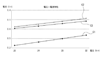
また、入力電流Iinの電流値は入力電圧Vinが変化することによっても変動する。
図3は、入力電圧Vinと入力電流Iinの関係の例を次の場合ごとに示している。すなわち、発光中素子数が0以外の最小値である場合(図中、特性C1)、発光中素子数が最大値である場合(図中、特性C2)である。なお、図3においては、各素子数増加タイミングにおいて発光中素子数を4ずつ増加させた場合の例を示している。すなわち、特性C1は発光中素子数=4の場合、特性C2は発光中素子数=20の場合の特性である。ここで、特性C1、C2は、後述する電流調整部38を用いた調整電流Imの調整が行われない場合の例を示すものである。
Further, the current value of the input current Iin also changes as the input voltage Vin changes.
FIG. 3 shows an example of the relationship between the input voltage Vin and the input current Iin in each of the following cases. That is, when the number of light emitting elements is the minimum value other than 0 (characteristic C1 in the figure) and the number of light emitting elements is the maximum value (characteristic C2 in the figure). Note that FIG. 3 shows an example in which the number of light emitting elements is increased by 4 at the timing of increasing the number of elements. That is, the characteristic C1 is a characteristic when the number of light emitting elements = 4, and the characteristic C2 is a characteristic when the number of light emitting elements = 20. Here, the characteristics C1 and C2 show an example in which the adjustment current Im is not adjusted by using the
図3の例の場合、入力電圧Vinの変動(例えば20V〜32Vの変動)によっては、入力電流Iinの電流値が特性C1の最小電流値(例えば0.25A)から特性C2の最大電流値(例えば1.15A)までの範囲で変動することが分かる。
このように入力電圧Vinが変化することによっても入力電流Iinの電流値は比較的大きく変動するものであり、従ってこの観点においても、ECU100側で断線判定を行う際の閾値THの設定が困難となり、適切な断線検知を行うことができない虞がある。
In the case of the example of FIG. 3, depending on the fluctuation of the input voltage Vin (for example, the fluctuation of 20V to 32V), the current value of the input current Iin changes from the minimum current value of the characteristic C1 (for example, 0.25A) to the maximum current value of the characteristic C2 (for example, 0.25A). For example, it can be seen that it fluctuates in the range up to 1.15A).
The current value of the input current Iin fluctuates relatively greatly even when the input voltage Vin changes in this way. Therefore, from this viewpoint as well, it becomes difficult to set the threshold value TH when determining the disconnection on the
なお、図3では参考として、発光素子20に白熱電球を用いた場合の特性C3を例示している。ここで、特性C3の場合、発光駆動回路3において電流消費部34は省略される。この特性C3に対し、特性C2(白熱電球よりも消費電力が小さいLEDが用いられる場合)が全域でより高い電流値を維持しているのは、調整電流Imにより入力電流Iinの電流値が嵩上げされるためである。
この点から理解されるように、電流消費部34を設けて調整電流Imを流すことは、白熱電球に対応する閾値THが設定されたECU100に対しても、適切な断線検知を可能にできるということを意味する。
Note that FIG. 3 exemplifies the characteristic C3 when an incandescent light bulb is used for the
As can be understood from this point, it is said that providing the current consuming
上記の問題点に鑑み、本実施形態においては発光中の発光素子20の数と、入力電圧Vinの電圧値とに応じて調整電流Imの電流値を調整する手法を採る。
このため、本実施形態の発光駆動回路3においては、図1に示すように、電流消費部34において抵抗部37と共に電流調整部38を設けている。
In view of the above problems, in the present embodiment, a method of adjusting the current value of the adjustment current Im according to the number of
Therefore, in the light emitting drive circuit 3 of the present embodiment, as shown in FIG. 1, the current consuming
抵抗部37は、入力フィルタ31とアース間に直列に挿入された1又は複数の抵抗素子を表しており、車載バッテリBtからの供給電力の一部を消費する。
電流調整部38は抵抗部37とアース間に挿入され、制御部33が出力する電流制御信号Sdaに基づき、調整電流Imの電流値を調整する。
The
The
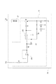
図4は、電流調整部38の内部構成を説明するための回路図であり、電流調整部38の内部回路構成例と共に抵抗部37を併せて示している。
図示のように電流調整部38は、抵抗R1、オペアンプOP1、抵抗R2、抵抗R3、オペアンプOP2、コンデンサC1、抵抗R4、抵抗R5、抵抗R6、抵抗R7、抵抗R8、及びトランジスタQ1を有している。
オペアンプOP1の正極入力端子には、抵抗R1を介して制御部33からの電流制御信号Sdaが入力される。オペアンプOP1は、出力端子が負極入力端子に接続され、ネガティブフィードバックループが形成されている。これによりオペアンプOP1は、ボルテージフォロワとして機能する。
FIG. 4 is a circuit diagram for explaining the internal configuration of the
As shown in the figure, the
The current control signal Sda from the
オペアンプOP1の出力端子は、抵抗R2を介してオペアンプOP2の正極入力端子に接続されている。抵抗R3は、オペアンプOP2の正極入力端子と、抵抗R2の接続点とアースとの間に挿入されている。
オペアンプOP2は、出力端子がコンデンサC1を介して負極入力端子に接続され、積分回路として機能する。
オペアンプOP2の出力端子は抵抗R8を介して、例えばNPN型のバイポーラトランジスタとされたトランジスタQ1のベースに接続されている。
The output terminal of the operational amplifier OP1 is connected to the positive electrode input terminal of the operational amplifier OP2 via the resistor R2. The resistor R3 is inserted between the positive electrode input terminal of the operational amplifier OP2, the connection point of the resistor R2, and the ground.
The output terminal of the operational amplifier OP2 is connected to the negative electrode input terminal via the capacitor C1 and functions as an integrating circuit.
The output terminal of the operational amplifier OP2 is connected to the base of the transistor Q1 which is, for example, an NPN type bipolar transistor, via the resistor R8.
オペアンプOP2の負極入力端子とコンデンサC1の接続点とアース間には、抵抗R4と、抵抗R5、抵抗R6及び抵抗R7の並列接続回路とが直列に挿入されている。
トランジスタQ1は、コレクタ−エミッタ間が抵抗部37と上記した抵抗R5、R6、R7による並列接続回路との間に挿入されており、調整電流Imを増幅する。
A resistor R4 and a parallel connection circuit of a resistor R5, a resistor R6, and a resistor R7 are inserted in series between the negative electrode input terminal of the operational amplifier OP2, the connection point of the capacitor C1, and the ground.
The transistor Q1 is inserted between the collector and the emitter between the
上記構成による電流調整部38においては、電流制御信号Sdaを入力するオペアンプOP1の出力電圧が抵抗R2と抵抗R3による分圧回路により分圧される。そして、オペアンプOP2は、トランジスタQ1のベース−エミッタ間の電位が上記分圧回路の分圧点に得られる電位と一致するようにトランジスタQ1にベース電流を流す。
これにより、電流制御信号Sdaの値を大きくするほど、トランジスタQ1における増幅率が大きくなり(換言すればコレクタ−エミッタ間の抵抗値が大きくなり)、調整電流Imの電流値が高くなる。
In the
As a result, as the value of the current control signal Sda increases, the amplification factor in the transistor Q1 increases (in other words, the resistance value between the collector and the emitter increases), and the current value of the adjustment current Im increases.
図5のフローチャートは、制御部33が電流制御信号Sdaを用いて行う電流調整部38の制御処理例を示している。
なお、図5に示す処理は、入力電圧VinがONとされて制御部33が起動したことに応じて開始される。
先ず、制御部33はステップS101で、タイミング識別値Nを「1」にセットする。タイミング識別値Nは、前述した素子数増加タイミングのうち、現在が何番目の素子数増加タイミングであるかを識別するための値である。
The flowchart of FIG. 5 shows an example of control processing of the
The process shown in FIG. 5 is started when the input voltage Vin is turned on and the
First, the
続くステップS102で制御部33は、入力電圧値取得処理として、入力電圧Vinの電圧値を取得する処理を行った上で、ステップS103でN灯目制御値計算処理を行う。すなわち、現在の発行中素子数と、ステップS102で取得した入力電圧Vinの電圧値とに基づいて、電流制御信号Sdaの値を計算する。具体的に本例では、電流制御信号Sdaの値を「DA」、現在の発行中素子数を「EA」、ステップS102で取得した入力電圧Vinの電圧値を「AD」としたとき、「EA」と「AD」を変数とした下記[式1]により電流制御信号Sdaの値を計算する。
DA={(AD×k1+k2−EA×k3)×4}−k4 …[式1]
ただし、k1〜k4は係数である。
In the following step S102, the
DA = {(AD x k1 + k2-EA x k3) x 4} -k4 ... [Equation 1]
However, k1 to k4 are coefficients.
続くステップS104で制御部33は、N灯目制御値出力処理として、ステップS103で計算した値による電流制御信号Sdaの出力を開始する。
In the following step S104, the
ステップS104の出力処理を行ったことに応じ、制御部33はステップS105でタイミング識別値Nが最大値Nmax以上であるか否かを判定する。本例では、Nmax=5である。
In response to the output processing in step S104, the
タイミング識別値Nが最大値Nmax以上でなければ、制御部33はステップS106で次の素子数増加タイミングが到来するまで待機し、次の素子数増加タイミングが到来した場合にはステップS107でタイミング識別値Nを1インクリメント(+1)し、ステップS102に戻る。これにより、発光中素子数が増加したことに対応して、増加後の発光中素子数と入力電圧Vinの値とに基づいた電流制御信号Sdaの値の再計算が行われ、出力される。
If the timing identification value N is not equal to or greater than the maximum value Nmax, the
また、制御部33は、ステップS105でタイミング識別値Nが最大値Nmax以上であれば、この図に示す処理を終える。
If the timing identification value N is equal to or greater than the maximum value Nmax in step S105, the
ここで、上記の[式1]は、入力電圧Vinが一定の下では、発光中素子数が少ない、つまり発光部2の消費電力が小さいほど値DAが大きくなるように設定されている。上述のように電流調整部38は値DAが大きいほど調整電流Imの電流値が高くなるように動作するため、結果、発光中素子数が少ないほど調整電流Imの電流値が高くなるように制御が行われる。換言すれば、発光中素子数が多いほど調整電流Imの電流値を低くする制御が行われる。
これにより、発光中素子数が少なく発光部2の消費電力が小さいことに起因して入力電流Iinの電流値が閾値THを下回ってしまうことの防止を図ることができ、発光素子20の断線検知の正確性向上を図ることができる。
Here, the above [Equation 1] is set so that the value DA increases as the number of elements during light emission is small, that is, the power consumption of the
As a result, it is possible to prevent the current value of the input current Iin from falling below the threshold value TH due to the small number of elements during light emission and the low power consumption of the
本例では、[式1]は、調整電流Imの電流値調整として、発光中素子数に拘わらず入力電流Iinの電流値を一定とする調整が行われるように設定されている(入力電圧Vinを一定とした場合)。
これにより、入力電流値が閾値THを上回る一定値で維持されるようにすることが可能とされ、発光素子20の断線検知の正確性をさらに向上させることができる。
In this example, [Equation 1] is set so that the current value of the adjustment current Im is adjusted so that the current value of the input current Iin is constant regardless of the number of elements during light emission (input voltage Vin). When is constant).
As a result, the input current value can be maintained at a constant value exceeding the threshold value TH, and the accuracy of disconnection detection of the
また、[式1]は、入力電圧Vinの電圧値が低いほど値DAが小さくなるように設定されている。つまりこれにより、入力電圧Vinが低いほど調整電流Imの電流値が低くなるように制御が行われる。
これにより、入力電圧Vinの低下に応じて入力電流Iinの電流値が低下する場合に対応して、電力消費部34による電力消費量が抑えられる。従って、入力電圧Vinの低下に起因して入力電流値が閾値TH以下に低下してしまうことの防止が図られ、発光素子20の断線検知の正確性向上を図ることができる。
Further, [Equation 1] is set so that the lower the voltage value of the input voltage Vin, the smaller the value DA. That is, as a result, control is performed so that the lower the input voltage Vin, the lower the current value of the adjustment current Im.
As a result, the power consumption by the
なお、上記では、調整電流Imの電流値調整を発光中素子数と入力電圧Vinとに基づき行う例を挙げたが、入力電圧Vinに基づく調整電流Imの電流値調整は必須ではない。 In the above, an example in which the current value of the adjustment current Im is adjusted based on the number of elements during light emission and the input voltage Vin is given, but the current value adjustment of the adjustment current Im based on the input voltage Vin is not essential.
また、上記では、値DAを逐次計算により取得する場合を例示したが、発光中素子数ごとに対応する値DAを格納したテーブルを用意しておき、現在の発光中素子数に対応する値DAを該テーブルから取得する構成とすることもできる。
入力電圧Vinに基づく調整電流Imの電流値調整を行う場合には、入力電圧Vinの電圧値ごとに上記のテーブルを用意しておき、それらのテーブルから現在の発光中素子数と入力電圧Vinの値とで特定される値DAを取得すればよい。
Further, in the above, the case where the value DA is acquired by sequential calculation is illustrated, but a table storing the corresponding value DA for each number of light emitting elements is prepared, and the value DA corresponding to the current number of light emitting elements is prepared. Can be obtained from the table.
When adjusting the current value of the adjustment current Im based on the input voltage Vin, prepare the above table for each voltage value of the input voltage Vin, and use those tables to determine the current number of light emitting elements and the input voltage Vin. The value DA specified by the value may be obtained.
上記のように実施形態としての発光駆動回路(同3)は、車載バッテリ(同Bt)からの電力供給に応じて複数の発光素子(同20)を有する発光部(同2)において発光素子が順に発光状態に遷移していく車両用灯具における発光駆動回路であって、車載バッテリからの電力供給ライン(同Ls)を介して供給される電流を受け、発光部におけるそれぞれの発光素子に駆動電流(同Id)を供給する電流供給部(同32)と、電力供給ラインより供給される電力の一部を消費して調整電流(同Im)を流す電流消費部(同34)と、発光部における発光中の発光素子の数が多いほど調整電流の電流値を低くする電流制御部(制御部33及び電流調整部38)と、を備えている。
As described above, in the light emitting drive circuit (3) as the embodiment, the light emitting element is in the light emitting unit (2) having a plurality of light emitting elements (20) according to the power supply from the vehicle-mounted battery (Bt). It is a light emitting drive circuit in a vehicle lighting device that sequentially transitions to a light emitting state, and receives a current supplied from an in-vehicle battery via a power supply line (Ls), and drives a current to each light emitting element in the light emitting unit. A current supply unit (32) that supplies (Id), a current consumption unit (34) that consumes a part of the power supplied from the power supply line and flows an adjusted current (Im), and a light emitting unit. It is provided with a current control unit (control
これにより、発光中素子数が少ない、つまり発光部の消費電力が小さいほど、調整電流の電流値を高くする制御が実現される。
従って、発光中素子数が少なく発光部の消費電力が小さいことに起因して入力電流値が断検閾値を下回ってしまうことの防止を図ることができ、発光素子の断線検知の正確性向上を図ることができる。
As a result, control is realized in which the current value of the adjustment current is increased as the number of elements during light emission is small, that is, the power consumption of the light emitting unit is small.
Therefore, it is possible to prevent the input current value from falling below the cutoff threshold due to the small number of elements during light emission and the low power consumption of the light emitting part, and improve the accuracy of disconnection detection of the light emitting element. Can be planned.
また、実施形態としての発光駆動回路においては、電流制御部は、発光中の発光素子の数と電力供給ラインからの入力電圧の電圧値とに基づいて調整電流の電流値を制御している。
入力電圧が低下すると入力電流値が低下し断検閾値以下に低下する虞がある。上記構成によれば、入力電圧の電圧値に基づいて調整電流の値が制御される、つまり電流消費部による電力消費量が制御されるため、入力電圧の低下に起因して入力電流値が断検閾値以下に低下してしまうことの防止を図ることが可能とされる。
従って、発光素子の断線検知の正確性向上を図ることができる。
Further, in the light emitting drive circuit as the embodiment, the current control unit controls the current value of the adjustment current based on the number of light emitting elements during light emission and the voltage value of the input voltage from the power supply line.
When the input voltage drops, the input current value drops and may drop below the cutoff threshold. According to the above configuration, the value of the adjustment current is controlled based on the voltage value of the input voltage, that is, the power consumption by the current consuming unit is controlled, so that the input current value is cut off due to the decrease in the input voltage. It is possible to prevent the voltage from dropping below the inspection threshold.
Therefore, it is possible to improve the accuracy of wire breakage detection of the light emitting element.
さらに、実施形態としての発光駆動回路においては、電流制御部は、入力電圧の電圧値が低いほど調整電流の電流値を低くしている。
これにより、入力電圧の低下に応じて入力電流値が低下する場合に対応して、電力消費部による電力消費量が抑えられる。
従って、入力電圧の低下に起因して入力電流値が断検閾値以下に低下してしまうことの防止が図られ、発光素子の断線検知の正確性向上を図ることができる。
Further, in the light emitting drive circuit as the embodiment, the current control unit lowers the current value of the adjustment current as the voltage value of the input voltage becomes lower.
As a result, the power consumption by the power consuming unit can be suppressed in response to the case where the input current value decreases as the input voltage decreases.
Therefore, it is possible to prevent the input current value from dropping below the disconnection threshold value due to the drop in the input voltage, and it is possible to improve the accuracy of disconnection detection of the light emitting element.
さらにまた、実施形態としての発光駆動回路においては、電流制御部は、電力供給ラインを流れる入力電流の電流値が発光部における発光中の発光素子の数に拘わらず一定となるように調整電流の電流値を制御している。
これにより、入力電流値が断検閾値を上回る一定値で維持されるようにすることが可能とされる。
従って、発光素子の断線検知の正確性をさらに向上させることができる。
Furthermore, in the light emitting drive circuit as the embodiment, the current control unit adjusts the current value of the input current flowing through the power supply line so as to be constant regardless of the number of light emitting elements in the light emitting unit. The current value is controlled.
This makes it possible to maintain the input current value at a constant value exceeding the cutoff threshold value.
Therefore, the accuracy of disconnection detection of the light emitting element can be further improved.
また、実施形態としての車両用灯具(同1)は、上記した実施形態としての発光駆動回路(同3)と発光部(同2)とを備えたものである。
この車両用灯具によっても、上記した実施形態としての発光駆動回路と同様の作用が得られる。すなわち、車載バッテリからの電力供給に応じて発光部における発光素子が順に発光状態に遷移していく車両用灯具について、発光素子の断線検知の正確性向上を図ることができる。
Further, the vehicle lamp (1) as the embodiment includes the light emitting drive circuit (3) and the light emitting unit (2) as the above-described embodiment.
With this vehicle lamp, the same operation as that of the light emitting drive circuit as the above-described embodiment can be obtained. That is, it is possible to improve the accuracy of the disconnection detection of the light emitting element in the vehicle lighting fixture in which the light emitting element in the light emitting unit sequentially transitions to the light emitting state according to the power supply from the in-vehicle battery.
なお、本発明は上記で説明した具体例に限定されるべきものでなく、多様な変形例が考えられる。
例えば、上記では、レギュレータIC35をON/OFFすることで発光素子を順に発光状態に遷移させていく例を挙げたが、発光素子20ごとにスイッチを設け、該スイッチをON/OFFすることで同様の発光態様を実現することもできる。
また、発光素子としては、例えば白熱電球等、LED以外の他の発光素子を用いることもできる。
The present invention should not be limited to the specific examples described above, and various modifications can be considered.
For example, in the above example, the light emitting elements are sequentially transitioned to the light emitting state by turning on / off the
Further, as the light emitting element, a light emitting element other than the LED, such as an incandescent light bulb, can also be used.
また、上記では、調整電流Imの生成に抵抗素子(抵抗部37)を用いる場合を例示したが、抵抗素子に代えて、例えばトランジスタを用いた定電流回路等の他の電力消費手段を用いることもできる。 Further, in the above, the case where the resistance element (resistance unit 37) is used to generate the adjustment current Im has been illustrated, but instead of the resistance element, another power consumption means such as a constant current circuit using a transistor may be used. You can also.
また、本発明は、ターンシグナルランプ以外であっても、車載バッテリからの電力供給に応じて発光部における発光素子が順に発光状態に遷移していく車両用灯具に好適に適用することができる。 Further, the present invention can be suitably applied to vehicle lamps other than turn signal lamps, in which the light emitting elements in the light emitting unit sequentially transition to the light emitting state according to the power supply from the in-vehicle battery.
1 車両用灯具、2 発光部、20−1、20−2、…、20−n 発光素子、3 発光駆動回路、32 電流供給部、33 制御部、34 電流消費部、35−1、35−2、…、35−n レギュレータIC(REG)、37 抵抗部、38 電流調整部、Ls 電力供給ライン、Iin 入力電流、Vin 入力電圧、Id1、Id2、…、Idn 駆動電流、Im 調整電流、St−1、St−2、…、St−n 発光制御信号、Sda 電流制御信号、100 ECU、Bt 車載バッテリ 1 Vehicle lighting equipment, 2 Light emitting unit, 20-1, 20-2, ..., 20-n light emitting element, 3 Light emitting drive circuit, 32 Current supply unit, 33 Control unit, 34 Current consumption unit, 35-1, 35- 2, ..., 35-n regulator IC (REG), 37 resistor part, 38 current adjustment part, Ls power supply line, Iin input current, Vin input voltage, Id1, Id2, ..., Idn drive current, Im adjustment current, St. -1, St-2, ..., Stn emission control signal, Sda current control signal, 100 ECU, Bt in-vehicle battery
Claims (5)
前記車載バッテリからの電力供給ラインを介して供給される電流を受け、前記発光部におけるそれぞれの前記発光素子に駆動電流を供給する電流供給部と、
前記電力供給ラインより供給される電力の一部を消費して調整電流を流す電流消費部と、
前記発光部における発光中の前記発光素子の数が多いほど前記調整電流の電流値を低くする電流制御部と、を備え、
前記電流制御部は、
発光中の前記発光素子の数と前記電力供給ラインからの入力電圧の電圧値とに基づいて前記調整電流の電流値を制御すると共に、前記入力電圧の電圧値に基づく前記調整電流の電流値制御を、発光中の前記発光素子の数が増加するごとに行う
発光駆動回路。 A light emitting drive circuit in a vehicle lamp in which the light emitting elements sequentially transition to a light emitting state in a light emitting unit having a plurality of light emitting elements according to power supply from an in-vehicle battery.
A current supply unit that receives a current supplied from the vehicle-mounted battery via a power supply line and supplies a drive current to each of the light emitting elements in the light emitting unit.
A current consuming unit that consumes a part of the power supplied from the power supply line to pass an adjusted current, and
A current control unit that lowers the current value of the adjustment current as the number of light emitting elements during light emission in the light emitting unit increases .
The current control unit
The current value of the adjustment current is controlled based on the number of the light emitting elements during light emission and the voltage value of the input voltage from the power supply line, and the current value control of the adjustment current based on the voltage value of the input voltage. A light emitting drive circuit that performs each time the number of the light emitting elements during light emission increases.
前記車載バッテリからの電力供給ラインを介して供給される電流を受け、前記発光部におけるそれぞれの前記発光素子に駆動電流を供給する電流供給部と、
前記電力供給ラインより供給される電力の一部を消費して調整電流を流す電流消費部と、
前記発光部における発光中の前記発光素子の数が多いほど前記調整電流の電流値を低くする電流制御部と、を備え、
前記電流制御部は、
発光中の前記発光素子の数と前記電力供給ラインからの入力電圧の電圧値とに基づいて前記調整電流の電流値を制御すると共に、
前記入力電圧の電圧値が低いほど前記調整電流の電流値を低くする
発光駆動回路。 A light emitting drive circuit in a vehicle lamp in which the light emitting elements sequentially transition to a light emitting state in a light emitting unit having a plurality of light emitting elements according to power supply from an in-vehicle battery.
A current supply unit that receives a current supplied from the vehicle-mounted battery via a power supply line and supplies a drive current to each of the light emitting elements in the light emitting unit.
A current consuming unit that consumes a part of the power supplied from the power supply line to pass an adjusted current, and
A current control unit that lowers the current value of the adjustment current as the number of light emitting elements during light emission in the light emitting unit increases.
The current control unit
The current value of the adjustment current is controlled based on the number of the light emitting elements during light emission and the voltage value of the input voltage from the power supply line, and the current value of the adjustment current is controlled .
A light emitting drive circuit that lowers the current value of the adjustment current as the voltage value of the input voltage is lower.
前記入力電圧の電圧値が低いほど前記調整電流の電流値を低くする
請求項1に記載の発光駆動回路。 The current control unit
The light emitting drive circuit according to claim 1 , wherein the lower the voltage value of the input voltage, the lower the current value of the adjustment current.
前記電力供給ラインを流れる入力電流の電流値が前記発光部における発光中の前記発光素子の数に拘わらず一定となるように前記調整電流の電流値を制御する
請求項1乃至請求項3の何れかに記載の発光駆動回路。 The current control unit
Any of claims 1 to 3 in which the current value of the adjustment current is controlled so that the current value of the input current flowing through the power supply line is constant regardless of the number of the light emitting elements during light emission in the light emitting unit. The light emitting drive circuit described in.
車両用灯具。 A vehicle lamp provided with the light emitting drive circuit according to any one of claims 1 to 4 and the light emitting unit.
Priority Applications (3)
| Application Number | Priority Date | Filing Date | Title |
|---|---|---|---|
| JP2017117849A JP6934331B2 (en) | 2017-06-15 | 2017-06-15 | Luminous drive circuit, vehicle lighting equipment |
| CN201820928943.4U CN208581368U (en) | 2017-06-15 | 2018-06-15 | Light emission drive circuit and lamps apparatus for vehicle |
| CN201810618317.XA CN109152129B (en) | 2017-06-15 | 2018-06-15 | Light emitting drive circuit and vehicle lamp |
Applications Claiming Priority (1)
| Application Number | Priority Date | Filing Date | Title |
|---|---|---|---|
| JP2017117849A JP6934331B2 (en) | 2017-06-15 | 2017-06-15 | Luminous drive circuit, vehicle lighting equipment |
Publications (2)
| Publication Number | Publication Date |
|---|---|
| JP2019001311A JP2019001311A (en) | 2019-01-10 |
| JP6934331B2 true JP6934331B2 (en) | 2021-09-15 |
Family
ID=64802077
Family Applications (1)
| Application Number | Title | Priority Date | Filing Date |
|---|---|---|---|
| JP2017117849A Active JP6934331B2 (en) | 2017-06-15 | 2017-06-15 | Luminous drive circuit, vehicle lighting equipment |
Country Status (2)
| Country | Link |
|---|---|
| JP (1) | JP6934331B2 (en) |
| CN (2) | CN109152129B (en) |
Families Citing this family (5)
| Publication number | Priority date | Publication date | Assignee | Title |
|---|---|---|---|---|
| JP6934331B2 (en) * | 2017-06-15 | 2021-09-15 | 株式会社小糸製作所 | Luminous drive circuit, vehicle lighting equipment |
| JP7432456B2 (en) | 2020-01-20 | 2024-02-16 | 株式会社小糸製作所 | Lighting circuit, vehicle direction indicator light |
| US20230045032A1 (en) * | 2020-01-20 | 2023-02-09 | Koito Manufacturing Co., Ltd. | Lighting circuit and vehicular direction indicator lamp |
| KR20210133646A (en) * | 2020-04-29 | 2021-11-08 | 에스엘 주식회사 | Lamp for vehicle |
| WO2022265083A1 (en) * | 2021-06-17 | 2022-12-22 | 株式会社小糸製作所 | Vehicle control system and ecu |
Family Cites Families (10)
| Publication number | Priority date | Publication date | Assignee | Title |
|---|---|---|---|---|
| JP2006172819A (en) * | 2004-12-14 | 2006-06-29 | Koito Mfg Co Ltd | Lighting control circuit of vehicular lighting fixture |
| JP2010083235A (en) * | 2008-09-30 | 2010-04-15 | Koito Mfg Co Ltd | Vehicular lamp |
| CN103959905B (en) * | 2011-10-31 | 2016-05-04 | 新电元工业株式会社 | The wire break detection method of direction lamp control device, direction indicating device and direction indicating device |
| DE102011119231A1 (en) * | 2011-11-23 | 2013-05-23 | Audi Ag | Motor vehicle light, motor vehicle and method for operating a motor vehicle light |
| DE102011088407A1 (en) * | 2011-12-13 | 2013-06-13 | Osram Gmbh | Circuit arrangement and method for operating an LED chain and lighting device with such a circuit arrangement and an LED chain |
| KR101974218B1 (en) * | 2012-05-04 | 2019-05-02 | 매그나칩 반도체 유한회사 | Led driver apparatus |
| JP6173874B2 (en) * | 2013-10-22 | 2017-08-02 | 株式会社小糸製作所 | Vehicle lighting |
| WO2016104282A1 (en) * | 2014-12-24 | 2016-06-30 | 株式会社小糸製作所 | Light source lighting circuit and turn signal lamp |
| JP6668648B2 (en) * | 2015-09-17 | 2020-03-18 | 市光工業株式会社 | Indicator light device |
| JP6934331B2 (en) * | 2017-06-15 | 2021-09-15 | 株式会社小糸製作所 | Luminous drive circuit, vehicle lighting equipment |
-
2017
- 2017-06-15 JP JP2017117849A patent/JP6934331B2/en active Active
-
2018
- 2018-06-15 CN CN201810618317.XA patent/CN109152129B/en active Active
- 2018-06-15 CN CN201820928943.4U patent/CN208581368U/en active Active
Also Published As
| Publication number | Publication date |
|---|---|
| CN109152129B (en) | 2021-01-29 |
| JP2019001311A (en) | 2019-01-10 |
| CN109152129A (en) | 2019-01-04 |
| CN208581368U (en) | 2019-03-05 |
Similar Documents
| Publication | Publication Date | Title |
|---|---|---|
| JP6934331B2 (en) | Luminous drive circuit, vehicle lighting equipment | |
| US7880401B2 (en) | Lighting controlling device of vehicle lighting equipment | |
| ES2323289T3 (en) | SYSTEM AND PROCEDURE OF LED ACTUATOR WITH FLOW COMPENSATION. | |
| JP5334372B2 (en) | Light emitting device | |
| JP4007097B2 (en) | Lighting device | |
| US8536790B2 (en) | LED lighting device and head lamp LED lighting device | |
| US20080297062A1 (en) | Illuminating device | |
| JP4799493B2 (en) | Vehicle lighting | |
| US10426012B2 (en) | Lighting circuit and vehicle lamp | |
| JP2009012669A (en) | Lighting control device for vehicular light | |
| JP2006210272A (en) | Led driving device and lighting device using it | |
| CN107770906B (en) | Hybrid dimming for lighting circuits | |
| US9775210B2 (en) | Lighting circuit, luminaire, and illumination system | |
| JP4187565B2 (en) | Lighting device | |
| US8390215B2 (en) | Light emitting diode circuit, light emitting diode driving circuit, voltage selection circuit, and method for driving thereof | |
| JP2008251320A (en) | Lighting circuit for vehicular lighting fixture | |
| JP2007004995A (en) | Led lighting device | |
| JP6173874B2 (en) | Vehicle lighting | |
| JP6249555B2 (en) | Vehicle lighting | |
| JP4416131B2 (en) | Lighting control device for vehicle lamp | |
| US10602579B2 (en) | Method for regulating an operating current of a lighting unit and control device and motor vehicle | |
| JP4259259B2 (en) | Indicator light device with multiple LEDs | |
| JP6337649B2 (en) | LED lamp unit and vehicle lamp device | |
| JP2007245760A (en) | Lighting circuit for vehicle lighting fixture | |
| JP3975800B2 (en) | Light control device for vehicle |
Legal Events
| Date | Code | Title | Description |
|---|---|---|---|
| A621 | Written request for application examination |
Free format text: JAPANESE INTERMEDIATE CODE: A621 Effective date: 20200515 |
|
| A977 | Report on retrieval |
Free format text: JAPANESE INTERMEDIATE CODE: A971007 Effective date: 20210319 |
|
| A131 | Notification of reasons for refusal |
Free format text: JAPANESE INTERMEDIATE CODE: A131 Effective date: 20210406 |
|
| A521 | Written amendment |
Free format text: JAPANESE INTERMEDIATE CODE: A523 Effective date: 20210604 |
|
| TRDD | Decision of grant or rejection written | ||
| A01 | Written decision to grant a patent or to grant a registration (utility model) |
Free format text: JAPANESE INTERMEDIATE CODE: A01 Effective date: 20210817 |
|
| A61 | First payment of annual fees (during grant procedure) |
Free format text: JAPANESE INTERMEDIATE CODE: A61 Effective date: 20210823 |
|
| R150 | Certificate of patent or registration of utility model |
Ref document number: 6934331 Country of ref document: JP Free format text: JAPANESE INTERMEDIATE CODE: R150 |