JP6924088B2 - Information processing equipment, its control method, and programs - Google Patents
Information processing equipment, its control method, and programs Download PDFInfo
- Publication number
- JP6924088B2 JP6924088B2 JP2017136439A JP2017136439A JP6924088B2 JP 6924088 B2 JP6924088 B2 JP 6924088B2 JP 2017136439 A JP2017136439 A JP 2017136439A JP 2017136439 A JP2017136439 A JP 2017136439A JP 6924088 B2 JP6924088 B2 JP 6924088B2
- Authority
- JP
- Japan
- Prior art keywords
- storage device
- data
- area
- storage
- information processing
- Prior art date
- Legal status (The legal status is an assumption and is not a legal conclusion. Google has not performed a legal analysis and makes no representation as to the accuracy of the status listed.)
- Active
Links
- 238000000034 method Methods 0.000 title claims description 113
- 230000010365 information processing Effects 0.000 title claims description 21
- 238000003860 storage Methods 0.000 claims description 488
- 238000013519 translation Methods 0.000 claims description 26
- 239000004065 semiconductor Substances 0.000 claims description 9
- 238000006243 chemical reaction Methods 0.000 claims description 5
- 230000003213 activating effect Effects 0.000 claims description 3
- 230000014759 maintenance of location Effects 0.000 description 23
- 238000012545 processing Methods 0.000 description 17
- 238000010586 diagram Methods 0.000 description 10
- 230000002093 peripheral effect Effects 0.000 description 9
- 230000007704 transition Effects 0.000 description 7
- 238000005192 partition Methods 0.000 description 6
- 230000000717 retained effect Effects 0.000 description 6
- KNMAVSAGTYIFJF-UHFFFAOYSA-N 1-[2-[(2-hydroxy-3-phenoxypropyl)amino]ethylamino]-3-phenoxypropan-2-ol;dihydrochloride Chemical compound Cl.Cl.C=1C=CC=CC=1OCC(O)CNCCNCC(O)COC1=CC=CC=C1 KNMAVSAGTYIFJF-UHFFFAOYSA-N 0.000 description 5
- 230000006870 function Effects 0.000 description 5
- 238000012546 transfer Methods 0.000 description 5
- 238000004891 communication Methods 0.000 description 3
- 238000005516 engineering process Methods 0.000 description 2
- 238000010438 heat treatment Methods 0.000 description 2
- 230000004044 response Effects 0.000 description 2
- 239000007787 solid Substances 0.000 description 2
- 238000012544 monitoring process Methods 0.000 description 1
- 238000007639 printing Methods 0.000 description 1
- 238000011084 recovery Methods 0.000 description 1
- 238000010998 test method Methods 0.000 description 1
Images


Classifications
-
- G—PHYSICS
- G06—COMPUTING; CALCULATING OR COUNTING
- G06F—ELECTRIC DIGITAL DATA PROCESSING
- G06F11/00—Error detection; Error correction; Monitoring
- G06F11/07—Responding to the occurrence of a fault, e.g. fault tolerance
- G06F11/16—Error detection or correction of the data by redundancy in hardware
- G06F11/20—Error detection or correction of the data by redundancy in hardware using active fault-masking, e.g. by switching out faulty elements or by switching in spare elements
- G06F11/2053—Error detection or correction of the data by redundancy in hardware using active fault-masking, e.g. by switching out faulty elements or by switching in spare elements where persistent mass storage functionality or persistent mass storage control functionality is redundant
- G06F11/2056—Error detection or correction of the data by redundancy in hardware using active fault-masking, e.g. by switching out faulty elements or by switching in spare elements where persistent mass storage functionality or persistent mass storage control functionality is redundant by mirroring
- G06F11/2069—Management of state, configuration or failover
-
- G—PHYSICS
- G06—COMPUTING; CALCULATING OR COUNTING
- G06F—ELECTRIC DIGITAL DATA PROCESSING
- G06F3/00—Input arrangements for transferring data to be processed into a form capable of being handled by the computer; Output arrangements for transferring data from processing unit to output unit, e.g. interface arrangements
- G06F3/06—Digital input from, or digital output to, record carriers, e.g. RAID, emulated record carriers or networked record carriers
- G06F3/0601—Interfaces specially adapted for storage systems
- G06F3/0602—Interfaces specially adapted for storage systems specifically adapted to achieve a particular effect
- G06F3/0625—Power saving in storage systems
-
- G—PHYSICS
- G06—COMPUTING; CALCULATING OR COUNTING
- G06F—ELECTRIC DIGITAL DATA PROCESSING
- G06F11/00—Error detection; Error correction; Monitoring
- G06F11/07—Responding to the occurrence of a fault, e.g. fault tolerance
- G06F11/08—Error detection or correction by redundancy in data representation, e.g. by using checking codes
- G06F11/10—Adding special bits or symbols to the coded information, e.g. parity check, casting out 9's or 11's
- G06F11/1076—Parity data used in redundant arrays of independent storages, e.g. in RAID systems
-
- G—PHYSICS
- G06—COMPUTING; CALCULATING OR COUNTING
- G06F—ELECTRIC DIGITAL DATA PROCESSING
- G06F11/00—Error detection; Error correction; Monitoring
- G06F11/07—Responding to the occurrence of a fault, e.g. fault tolerance
- G06F11/16—Error detection or correction of the data by redundancy in hardware
- G06F11/20—Error detection or correction of the data by redundancy in hardware using active fault-masking, e.g. by switching out faulty elements or by switching in spare elements
- G06F11/2053—Error detection or correction of the data by redundancy in hardware using active fault-masking, e.g. by switching out faulty elements or by switching in spare elements where persistent mass storage functionality or persistent mass storage control functionality is redundant
- G06F11/2056—Error detection or correction of the data by redundancy in hardware using active fault-masking, e.g. by switching out faulty elements or by switching in spare elements where persistent mass storage functionality or persistent mass storage control functionality is redundant by mirroring
- G06F11/2082—Data synchronisation
-
- G—PHYSICS
- G06—COMPUTING; CALCULATING OR COUNTING
- G06F—ELECTRIC DIGITAL DATA PROCESSING
- G06F3/00—Input arrangements for transferring data to be processed into a form capable of being handled by the computer; Output arrangements for transferring data from processing unit to output unit, e.g. interface arrangements
- G06F3/06—Digital input from, or digital output to, record carriers, e.g. RAID, emulated record carriers or networked record carriers
- G06F3/0601—Interfaces specially adapted for storage systems
- G06F3/0602—Interfaces specially adapted for storage systems specifically adapted to achieve a particular effect
- G06F3/0614—Improving the reliability of storage systems
- G06F3/0619—Improving the reliability of storage systems in relation to data integrity, e.g. data losses, bit errors
-
- G—PHYSICS
- G06—COMPUTING; CALCULATING OR COUNTING
- G06F—ELECTRIC DIGITAL DATA PROCESSING
- G06F3/00—Input arrangements for transferring data to be processed into a form capable of being handled by the computer; Output arrangements for transferring data from processing unit to output unit, e.g. interface arrangements
- G06F3/06—Digital input from, or digital output to, record carriers, e.g. RAID, emulated record carriers or networked record carriers
- G06F3/0601—Interfaces specially adapted for storage systems
- G06F3/0628—Interfaces specially adapted for storage systems making use of a particular technique
- G06F3/0646—Horizontal data movement in storage systems, i.e. moving data in between storage devices or systems
- G06F3/065—Replication mechanisms
-
- G—PHYSICS
- G06—COMPUTING; CALCULATING OR COUNTING
- G06F—ELECTRIC DIGITAL DATA PROCESSING
- G06F3/00—Input arrangements for transferring data to be processed into a form capable of being handled by the computer; Output arrangements for transferring data from processing unit to output unit, e.g. interface arrangements
- G06F3/06—Digital input from, or digital output to, record carriers, e.g. RAID, emulated record carriers or networked record carriers
- G06F3/0601—Interfaces specially adapted for storage systems
- G06F3/0628—Interfaces specially adapted for storage systems making use of a particular technique
- G06F3/0655—Vertical data movement, i.e. input-output transfer; data movement between one or more hosts and one or more storage devices
- G06F3/0658—Controller construction arrangements
-
- G—PHYSICS
- G06—COMPUTING; CALCULATING OR COUNTING
- G06F—ELECTRIC DIGITAL DATA PROCESSING
- G06F3/00—Input arrangements for transferring data to be processed into a form capable of being handled by the computer; Output arrangements for transferring data from processing unit to output unit, e.g. interface arrangements
- G06F3/06—Digital input from, or digital output to, record carriers, e.g. RAID, emulated record carriers or networked record carriers
- G06F3/0601—Interfaces specially adapted for storage systems
- G06F3/0668—Interfaces specially adapted for storage systems adopting a particular infrastructure
- G06F3/0671—In-line storage system
- G06F3/0683—Plurality of storage devices
- G06F3/0685—Hybrid storage combining heterogeneous device types, e.g. hierarchical storage, hybrid arrays
-
- G—PHYSICS
- G06—COMPUTING; CALCULATING OR COUNTING
- G06F—ELECTRIC DIGITAL DATA PROCESSING
- G06F3/00—Input arrangements for transferring data to be processed into a form capable of being handled by the computer; Output arrangements for transferring data from processing unit to output unit, e.g. interface arrangements
- G06F3/06—Digital input from, or digital output to, record carriers, e.g. RAID, emulated record carriers or networked record carriers
- G06F3/0601—Interfaces specially adapted for storage systems
- G06F3/0668—Interfaces specially adapted for storage systems adopting a particular infrastructure
- G06F3/0671—In-line storage system
- G06F3/0683—Plurality of storage devices
- G06F3/0689—Disk arrays, e.g. RAID, JBOD
-
- G—PHYSICS
- G06—COMPUTING; CALCULATING OR COUNTING
- G06F—ELECTRIC DIGITAL DATA PROCESSING
- G06F11/00—Error detection; Error correction; Monitoring
- G06F11/07—Responding to the occurrence of a fault, e.g. fault tolerance
- G06F11/16—Error detection or correction of the data by redundancy in hardware
- G06F11/20—Error detection or correction of the data by redundancy in hardware using active fault-masking, e.g. by switching out faulty elements or by switching in spare elements
- G06F11/2053—Error detection or correction of the data by redundancy in hardware using active fault-masking, e.g. by switching out faulty elements or by switching in spare elements where persistent mass storage functionality or persistent mass storage control functionality is redundant
- G06F11/2056—Error detection or correction of the data by redundancy in hardware using active fault-masking, e.g. by switching out faulty elements or by switching in spare elements where persistent mass storage functionality or persistent mass storage control functionality is redundant by mirroring
- G06F11/2087—Error detection or correction of the data by redundancy in hardware using active fault-masking, e.g. by switching out faulty elements or by switching in spare elements where persistent mass storage functionality or persistent mass storage control functionality is redundant by mirroring with a common controller
-
- G—PHYSICS
- G06—COMPUTING; CALCULATING OR COUNTING
- G06F—ELECTRIC DIGITAL DATA PROCESSING
- G06F2201/00—Indexing scheme relating to error detection, to error correction, and to monitoring
- G06F2201/82—Solving problems relating to consistency
-
- Y—GENERAL TAGGING OF NEW TECHNOLOGICAL DEVELOPMENTS; GENERAL TAGGING OF CROSS-SECTIONAL TECHNOLOGIES SPANNING OVER SEVERAL SECTIONS OF THE IPC; TECHNICAL SUBJECTS COVERED BY FORMER USPC CROSS-REFERENCE ART COLLECTIONS [XRACs] AND DIGESTS
- Y02—TECHNOLOGIES OR APPLICATIONS FOR MITIGATION OR ADAPTATION AGAINST CLIMATE CHANGE
- Y02D—CLIMATE CHANGE MITIGATION TECHNOLOGIES IN INFORMATION AND COMMUNICATION TECHNOLOGIES [ICT], I.E. INFORMATION AND COMMUNICATION TECHNOLOGIES AIMING AT THE REDUCTION OF THEIR OWN ENERGY USE
- Y02D10/00—Energy efficient computing, e.g. low power processors, power management or thermal management
Description
本発明は、画像形成装置等の情報処理装置及びその制御方法、並びにプログラムに関するものである。 The present invention relates to an information processing device such as an image forming device, a control method thereof, and a program.
記憶装置に保存されるデータの信頼性の向上のために、2台のストレージ内に同じデータを保持することによってデータの信頼性を向上させるRAID1(ミラーリング)システムを備える画像形成装置が知られている(例えば、特許文献1)。ミラーリングシステムでは、1台のストレージが故障した場合、故障したストレージを新しいストレージに交換することにより、データを復旧することが可能である。 In order to improve the reliability of data stored in a storage device, an image forming apparatus equipped with a RAID1 (mirroring) system that improves the reliability of data by holding the same data in two storages is known. (For example, Patent Document 1). In the mirroring system, when one storage fails, the data can be recovered by replacing the failed storage with a new storage.
また、ミラーリングシステムは、2つのストレージの一方をマスターに設定し、他方をスレーブに設定し、データのライト(書き込み)及びリード(読み出し)を制御する。具体的には、ミラーリングシステムは、マスター及びスレーブのストレージの両方にデータのライトを行って、2つのストレージ内に同じデータを保持しながら、一方のストレージからデータのリードを行う。スレーブ側へ新たなストレージを接続(増設)した場合、2つのストレージに同じデータを保持させるために、マスターストレージからスレーブストレージへデータをコピーする処理(リビルド処理)が行われる。 The mirroring system also sets one of the two storages as a master and the other as a slave to control data write and read. Specifically, the mirroring system writes data to both master and slave storage and reads data from one storage while retaining the same data in the two storages. When a new storage is connected (added) to the slave side, a process of copying data from the master storage to the slave storage (rebuild process) is performed in order to hold the same data in the two storages.
上述のようなミラーリングシステムでは、各ストレージとして、HDDが使用されるだけでなく、近年ではSSDが使用される場合がある。一般に、SSDは、フラッシュメモリ(半導体メモリ)で構成されるため、HDDよりも高いデータ転送速度を有するものの、データの書き換え回数及び保持期間に制限がある。特許文献2では、SSDのデータの書き換え回数の制限に対処するために、マスターに設定されたSSDのデータ書き換え回数に基づいて、SSDをスレーブに変更し、HDDをマスターに変更することで、ミラーリング制御の信頼性を向上させている。 In the mirroring system as described above, not only HDD is used as each storage, but SSD may be used in recent years. Generally, since an SSD is composed of a flash memory (semiconductor memory), it has a higher data transfer rate than an HDD, but there are restrictions on the number of times data can be rewritten and the retention period. In Patent Document 2, in order to deal with the limitation on the number of times the SSD data can be rewritten, the SSD is changed to the slave and the HDD is changed to the master based on the number of times the SSD data is rewritten set in the master, thereby mirroring. It improves the reliability of control.
また、SSDでは、一定時間アクセスが行われないことで、データの保持期間の制限に起因してデータが消失することを防ぐために、SSDのリフレッシュ動作を行う必要がある。SSDにおいてデータが消失せずに保持される保持期間は、データの書き込み時及び電源OFF時における、SSD内部のフラッシュメモリの温度に依存して変化することが知られている。具体的には、データの書き込み時のフラッシュメモリの温度が高いほど、保持期間が長くなり、電源OFF時のフラッシュメモリの温度が低いほど、保持期間が長くなる(非特許文献1)。 Further, in the SSD, it is necessary to perform the SSD refresh operation in order to prevent the data from being lost due to the limitation of the data retention period due to the fact that the SSD is not accessed for a certain period of time. It is known that the retention period in which data is retained in the SSD without being lost depends on the temperature of the flash memory inside the SSD when the data is written and when the power is turned off. Specifically, the higher the temperature of the flash memory at the time of writing data, the longer the holding period, and the lower the temperature of the flash memory at the time of turning off the power, the longer the holding period (Non-Patent Document 1).
SSDを使用するミラーリングシステムにおいて、スレーブ側に接続されたSSDに対してリビルド処理を行う際に、内部のフラッシュメモリの温度が低いときにデータのコピー(ライト)を行うと、SSDによるデータの保持期間が短くなる。その結果、SSDへのデータのコピーの完了後に、例えば、当該SSDが搭載された画像形成装置等の情報処理装置において電源OFF状態が継続すると、短い期間でデータが消失してしまう可能性がある。システムデータ等の、長期間保持されることが望ましいデータについては、短期間のうちに消失することを防ぐ必要がある。 In a mirroring system that uses SSD, when rebuilding the SSD connected to the slave side, if data is copied (written) when the temperature of the internal flash memory is low, the data will be retained by the SSD. The period will be shorter. As a result, if the power off state continues in an information processing device such as an image forming device equipped with the SSD after the completion of copying the data to the SSD, the data may be lost in a short period of time. .. Data that should be retained for a long period of time, such as system data, needs to be prevented from being lost in a short period of time.
本発明は、上述の問題に鑑みて成されたものである。本発明は、半導体メモリで構成された記憶装置(SSD)に対してミラーリングのためにリビルド処理を行う場合に、SSDにコピーされたデータの保持期間をより長くする技術を提供することを目的とする。 The present invention has been made in view of the above problems. An object of the present invention is to provide a technique for extending the retention period of data copied to an SSD when performing a rebuild process for mirroring on a storage device (SSD) composed of a semiconductor memory. do.
本発明の一態様に係る情報処理装置は、前記情報処理装置の起動に用いるシステムデータが記憶領域の先頭部の領域に格納された第1記憶装置と、前記第1記憶装置との間でデータのミラーリングが行われる第2記憶装置と、前記第1記憶装置に格納されたデータを前記第2記憶装置にコピーすることによって前記第2記憶装置のリビルド処理を行う制御手段と、を備え、前記制御手段は、前記第2記憶装置が半導体メモリで構成された第1タイプの記憶装置であれば、前記リビルド処理において、前記第1記憶装置に格納されたデータのうち、前記システムデータ以外のデータを前記第2記憶装置にコピーした後に、前記システムデータを前記第2記憶装置へコピーし、前記制御手段は、前記第2記憶装置が磁気ディスクで構成された第2タイプの記憶装置であれば、前記第1記憶装置の記憶領域の前記先頭部の領域から最後部の領域まで順に、各領域に格納されているデータを読み出し、前記第1記憶装置から順に読み出したデータを、前記第2記憶装置の記憶領域における前記先頭部の領域から前記最後部の領域まで順に書き込むことを特徴とする。 The information processing device according to one aspect of the present invention is data between the first storage device in which the system data used for activating the information processing device is stored in the region at the head of the storage area and the first storage device. A second storage device for which mirroring is performed, and a control means for rebuilding the second storage device by copying the data stored in the first storage device to the second storage device. control means, wherein if the second storage device of a first type of storage device configured by a semiconductor memory, in the rebuild process, among the data stored in the first storage device, the data other than the system data Is copied to the second storage device, and then the system data is copied to the second storage device. If the control means is a second type storage device in which the second storage device is composed of a magnetic disk. , The data stored in each area is read out in order from the head region to the last region of the storage area of the first storage device, and the data read out in order from the first storage device is stored in the second storage device. It is characterized in that writing is performed in order from the head region to the rear end region in the storage area of the device.
本発明によれば、半導体メモリで構成された記憶装置(SSD)に対してミラーリングのためにリビルド処理を行う場合に、SSDにコピーされたデータの保持期間をより長くすることが可能になる。 According to the present invention, when a rebuild process is performed for mirroring on a storage device (SSD) composed of a semiconductor memory, it is possible to extend the retention period of the data copied to the SSD.
以下では、添付図面を参照して本発明の実施形態を詳しく説明する。なお、以下の実施形態は特許請求の範囲に係る本発明を限定するものでなく、また本実施形態で説明されている特徴の組み合わせの全てが本発明の解決手段に必須のものとは限らない。 Hereinafter, embodiments of the present invention will be described in detail with reference to the accompanying drawings. It should be noted that the following embodiments do not limit the present invention according to the claims, and not all combinations of features described in the present embodiment are essential for the means for solving the present invention. ..
<画像形成装置>
図1(A)は、画像形成装置10の概略的なハードウェア構成例を示すブロック図である。画像形成装置10は、本発明の情報処理装置の一例である。なお、画像形成装置10は、後述するようなミラーリングシステムを搭載していれば、例えば、印刷装置、プリンタ、複写機、複合機(MFP)、及びファクシミリ装置のいずれとして構成されてもよい。画像形成装置10は、コントローラ部200と、コントローラ部200と接続されたスキャナ部300、プリンタ部400、及び操作部500とを備える。コントローラ部200は、CPU201、RAM202、ROM203、LANコントローラ204、電源制御部205、画像処理部206、及びRAID部250を備える。コントローラ部200は、RAID部250に接続されたストレージとして、記憶装置A(208)及び記憶装置B(209)を備える。
<Image forming device>
FIG. 1A is a block diagram showing a schematic hardware configuration example of the
電源制御部205は、電源から画像形成装置10内の各デバイスへの電力の供給状態を制御する。CPU201は、電源制御部205により電源が投入されると、ブートプログラムをROM203から読み出して実行することにより、画像形成装置10の起動処理を行う。また、CPU201は、RAID部250に接続された記憶装置Aから制御プログラム又はアプリケーションプログラム等の各種プログラムをRAM202に展開して実行することにより、画像形成装置10の各種機能を実現する。
The power
LANコントローラ204は、LAN等のネットワークに接続されており、ネットワークを介してPC等の外部装置と通信する。CPU201は、例えば、LANコントローラ204を介して外部装置からプリントデータ等の各種データを受信できる。なお、画像形成装置10は、外部装置と無線通信(無線LAN通信等)を行うための無線通信インタフェース(I/F)を備えていてもよい。
The
スキャナ部300は、原稿の画像を読み取って画像データを生成する。スキャナ部300は、生成した画像データを、スキャナI/F211を介してシステムバス210へ送信する。プリンタ部400は、システムバス210を介して受信した画像データに基づいてプリント処理を行う。操作部500は、CPU201からの指示に従って操作画面を表示し、また、ユーザから受け付けた指示をCPU201へ通知する。
The
CPU201は、LANコントローラ204によって外部装置から印刷データが受信されると、受信した印刷データを、RAM202を経由して記憶装置Aに一時的に保存する。更に、CPU201は、画像処理部206によって当該印刷データに対する画像処理が行われた後、当該印刷データをプリンタ部400へ送信することにより、プリンタ部400にプリント処理を実行させる。また、CPU201は、コピー機能を実現する場合には、スキャナ部300によって生成された画像データをプリンタ部400へ送信することにより、プリンタ部400にプリント処理を実行させる。
When the print data is received from the external device by the
RAID部250には、画像形成装置10において二次記憶装置(補助記憶装置)として使用される、少なくとも1台の不揮発性のストレージが接続される。図1は、画像形成装置10が、記憶装置A及び記憶装置Bの、2台のストレージを備える例を示している。記憶装置Aは、RAID部250のチャネルAに接続されるストレージであり、記憶装置Bは、RAID部250のチャネルBに接続されるストレージである。本実施形態では、記憶装置A及び記憶装置Bのそれぞれは、HDD(ハードディスクドライブ)又はSSD(ソリッドステートドライブ)である。なお、SSDは、半導体メモリで構成された第1タイプの記憶装置の一例であり、HDDは、磁気ディスクで構成された第2タイプの記憶装置の一例である。画像形成装置10のシステムの起動に必要なシステムデータは、記憶装置A及び記憶装置Bのうちの一方に格納される。システムデータが格納された記憶装置がRAID部250に接続されると、当該システムデータに基づいて、画像形成装置10のシステムが起動可能になる。
At least one non-volatile storage used as a secondary storage device (auxiliary storage device) in the
RAID部250と、RAID部250に接続されたストレージ(図1では記憶装置A及び記憶装置B)は、RAID1(ミラーリング)システムを構成する。RAID1は、2台以上のストレージに同じデータを保持させることにより、1台のストレージが故障した場合でも、故障したストレージに格納されていたデータの復旧を可能にする技術である。RAID部250は、ミラーリング制御を行う。図1の構成では、RAID部250がミラーリング制御を行うことにより、システムバス210側(CPU201側)では、複数台のストレージがあたかも1台のストレージであるかのように認識される。なお、後述する実施例3及び4のように、CPU201がミラーリング制御を行う構成を採用することも可能である。
The
RAID部250が、ミラーリング制御を行う場合、記憶装置A及び記憶装置Bのうちの一方がマスターに設定され、他方がスレーブに設定される。ミラーリング制御において、RAID部250は、データのライトを行う場合には、マスターストレージ及びスレーブストレージの両方にデータを書き込み、データのリードを行う場合には、マスターストレージからデータの読み出しを行う。なお、マスターストレージはチャネルA及びBのいずれのチャネルに接続されてもよいが、本実施形態ではチャネルAにマスターストレージが接続される場合を想定する。また、RAID部250は、後述するように、スレーブストレージの増設又は故障したストレージの交換が行われる際に、新たに接続されたストレージのリビルド処理を制御する。
When the
<RAID部>
図1(B)は、RAID部250の構成例を示すブロック図である。RAID部250は、RAIDコントローラ251、フォーマット管理部252、アドレス変換部253、及び状態保持部254を備える。RAIDコントローラ251は、フォーマット管理部252、アドレス変換部253、及び状態保持部254を使用して、RAID部250に接続された記憶装置A及び記憶装置B間でミラーリング(RAID1)を行う。RAIDコントローラ251は、システムバス210を介してCPU201からコマンド(命令)を受信し、受信したコマンドに従って、ミラーリングのための処理を実行する。なお、チャネルAに記憶装置Aが接続され、チャネルBに記憶装置Bが未接続である場合は、RAIDコントローラ251は、CPU201から受信したコマンドを、そのまま記憶装置Aに送信する。
<RAID section>
FIG. 1B is a block diagram showing a configuration example of the
フォーマット管理部252は、記憶装置A及び記憶装置Bのそれぞれの記憶領域におけるパーティション構成を示す管理情報を保持している。状態保持部254は、RAIDコントローラ251、フォーマット管理部252、アドレス変換部253、及び状態保持部254の初期値を保持している。状態保持部254は、更に、RAIDコントローラ251に接続された各記憶装置のタイプ(HDD又はSSD)、及び接続された記憶装置の台数を保持している。
The format management unit 252 holds management information indicating the partition configuration in each storage area of the storage device A and the storage device B. The
RAIDコントローラ251は、ミラーリングを行う際、マスターストレージ(記憶装置A)のID、及び当該マスターストレージの記憶領域におけるアクセス対象の領域を示すLBA(Logical Block Addressing)値を、アドレス変換部253へ送る。アドレス変換部253は、フォーマット管理部252及び状態保持部254が保持している情報に基づいて、スレーブストレージ(記憶装置B)の記憶領域におけるアクセス対象の領域を示すLBA値を取得する。即ち、アドレス変換部253は、マスターストレージ(記憶装置A)のLBA値を、スレーブストレージ(記憶装置B)の、対応するLBA値に変換する。アドレス変換部253は、取得したLBA値をRAIDコントローラ251へ送る。これにより、RAIDコントローラ251は、マスターストレージにおけるアクセス対象の記憶領域と、それに対応する、スレーブストレージにおける記憶領域とにアクセスし、ミラーリングを行うことが可能になる。
When performing mirroring, the
<RAIDコントローラの状態遷移>
図2は、RAIDコントローラ251の状態遷移の例を示す図である。RAIDコントローラ251は、シングルモード及びミラーリングモードの、2つの動作モードを有する。シングルモードは、1台のストレージのみを使用する動作モードである。ミラーリングモードは、2台以上のストレージを使用する動作モードである。
<State transition of RAID controller>
FIG. 2 is a diagram showing an example of a state transition of the
シングルモードでは、記憶装置A及び記憶装置BのいずれかがRAID部250(RAIDコントローラ251)に接続される。ミラーリングモードでは、RAIDコントローラ251は、先に接続されていた記憶装置をマスターに設定し、後から追加された記憶装置をスレーブに設定する。例えば、シングルモードにおいて記憶装置Aが接続されている場合、RAIDコントローラ251は、シングルモードからミラーリングモードへ移行する際に、記憶装置Aをマスターに設定する。RAIDコントローラ251は、記憶装置Bが追加で接続されると、記憶装置Bをスレーブに設定する。
In the single mode, either the storage device A or the storage device B is connected to the RAID unit 250 (RAID controller 251). In the mirroring mode, the
ミラーリングモードには、ミラーステート、デグレードステート、リビルドステート、及びホールトステートの、4つの状態(ステート)が存在する。シングルモードにおいて1台のストレージが追加で接続されると、RAIDコントローラ251は、当該ストレージをスレーブに設定し、ミラーリングモードのリビルドステートへ移行する(301)。
There are four states (states) in the mirroring mode: a mirror state, a degraded state, a rebuild state, and a held state. When one storage unit is additionally connected in the single mode, the
リビルドステートは、RAIDコントローラ251がマスターストレージのみを使用して動作している状態であり、かつ、マスターストレージからスレーブストレージへのデータのコピー(スレーブストレージのリビルド処理)を行っている状態である。リビルドステートにおいてリビルド処理が完了すると、RAIDコントローラ251は、ミラーステートへ移行する(302)。また、RAIDコントローラ251は、リビルドステートにおいてスレーブストレージが故障した場合、デグレードステートへ移行し(303)、リビルドステートにおいてマスターストレージが故障した場合、ホールトステートへ移行する(304)。
The rebuild state is a state in which the
ミラーステートは、RAIDコントローラ251が2台のストレージ(マスターストレージ及びスレーブストレージ)を使用して正常に動作している(即ち、2台のストレージ間でミラーリングを行う)状態である。RAIDコントローラ251は、ミラーステートでは、読み出しはマスターストレージのみに対して行い、書き込みはマスターストレージ及びスレーブストレージの両方に対して行う。ミラーステートにおいて2台のストレージのうちの一方のストレージが故障すると、RAIDコントローラ251は、デグレードステートへ移行する(305)。また、ミラーステートにおいて、リビルドステートへの移行命令をCPU201から受信すると、RAIDコントローラ251は、リビルドステートへ移行する(306)。
The mirror state is a state in which the
デグレードステートは、RAIDコントローラ251が、故障していないストレージのみを使用して動作している状態であり、故障したストレージへのアクセスが発生しない状態である。デグレードステートにおいて使用中のストレージが故障すると(即ち、2台のストレージの両方が故障した状態になると)、RAIDコントローラ251は、ホールトステートへ移行する(307)。また、デグレードステートにおいて、リビルドステートへの移行命令をCPU201から受信すると、RAIDコントローラ251は、リビルドステートへ移行する(308)。例えば、故障したストレージが新しいストレージに交換された後に、CPU201からRAIDコントローラ251に対してリビルドステートへの移行命令が送信される。
The degraded state is a state in which the
ホールトステートは、2台のストレージの両方が故障したことにより、RAIDコントローラ251がミラーリングを継続できなくなった状態である。なお、RAIDコントローラ251は、ミラーリングモードの4つの状態の何れにおいても、シングルモードへの移行指示をユーザから受け付けると、ミラーリングモードからシングルモードへ移行する(309)。
The halt state is a state in which the
<スレーブストレージのリビルド処理>
上述のように、画像形成装置10は、記憶装置A(第1記憶装置)に加えて、記憶装置B(第2記憶装置)が接続(増設)されることにより、記憶装置Aと記憶装置Bとの間でデータのミラーリングが行われる。以下では、記憶装置Aがマスターストレージとして設定され、記憶装置Bがスレーブストレージとして設定される場合を例として、記憶装置Bが接続(増設)された際に実行されるリビルド処理について説明する。リビルド処理は、以下の実施例1及び2では、RAIDコントローラ251によって実行される。なお、実施例3及び4のように、RAID部250が設けられていない場合には、CPU201によって実行されうる。即ち、RAIDコントローラ251又はCPU201は、記憶装置Aに格納されたデータを記憶装置Bにコピーすることによって記憶装置Bのリビルド処理を行う制御手段の一例として機能する。
<Slave storage rebuild process>
As described above, in the
リビルド処理の対象となる記憶装置BがSSDである場合、上述のように、SSD内部のフラッシュメモリの温度が低いときにデータの書き込みを行うと、SSDによるデータの保持期間が短くなる。一方、SSDへのデータの書き込み時におけるフラッシュメモリの温度が高いほど、データの保持期間が長くなる。このため、SSDによって長期間保持されるべき(例えば、書き換え頻度の少ない)データは、SSD内のフラッシュメモリの温度が自己昇温により高くなってからSSDへコピーされることが望まれる。ここで、画像形成装置10においては、記憶装置Aのシステム領域に格納された、画像形成装置10のシステムデータは、長期間保持されるべきデータに相当する。このシステムデータには、例えば、システムの起動に必要な起動データ、及びシステムによって使用されるデータ等のシステム関連データが含まれる。
When the storage device B to be rebuilt is an SSD, if data is written when the temperature of the flash memory inside the SSD is low as described above, the data retention period by the SSD is shortened. On the other hand, the higher the temperature of the flash memory when writing data to the SSD, the longer the data retention period. Therefore, it is desirable that the data that should be retained by the SSD for a long period of time (for example, the frequency of rewriting is low) is copied to the SSD after the temperature of the flash memory in the SSD rises due to self-heating. Here, in the
そこで、本実施形態では、記憶装置Aに格納されたデータのうち、画像形成装置10のシステムデータを、リビルド処理の開始後、できるだけ遅いタイミングに記憶装置B(SSD)へコピーするよう、リビルド処理を制御する。具体的には、記憶装置BがSSDであれば、リビルド処理において、記憶装置Aに格納されたデータのうち、画像形成装置10のシステムデータ以外のデータを記憶装置Bにコピーした後に、当該システムデータを記憶装置Bへコピーする。即ち、記憶装置Aから記憶装置Bへコピーされるデータのうち、システムデータを他のデータよりも遅いタイミング(例えば最後に)コピーする。これにより、画像形成装置10の起動後に実行されるリビルド処理において、記憶装置B(SSD)内のフラッシュメモリの温度が高くなってから、システムデータを記憶装置Aから記憶装置Bへコピーすることが可能になる。その結果、例えば画像形成装置10において電源OFF状態が継続するような状況が生じても、短い期間でシステムデータが記憶装置Bから消失することを防止できる。
Therefore, in the present embodiment, the rebuild process is performed so that the system data of the
以下、上述のリビルド処理の具体例として実施例1〜4について説明する。なお、記憶装置A及び記憶装置Bには、画像形成装置10のシステムの動作に必要となる一定容量以上の記憶容量を有する記憶装置が使用される。また、各記憶装置では、システムによって全ての容量が必ずしも使用されるのではなく、システムに対して予め設定された一部の容量が使用されうる。
Hereinafter, Examples 1 to 4 will be described as specific examples of the above-mentioned rebuild process. As the storage device A and the storage device B, a storage device having a storage capacity of a certain capacity or more required for the operation of the system of the
[実施例1]
実施例1では、RAIDコントローラ251は、記憶装置BがSSDであれば、リビルド処理において、記憶装置Aの記憶領域における最後部の領域から先頭部の領域まで順に、各領域に格納されているデータを記憶装置Bへコピーする。これにより、記憶装置Aに格納されたデータのうちで、記憶装置Aの記憶領域における先頭部の領域に格納されたシステムデータが最後にコピーされる。したがって、記憶装置B内のフラッシュメモリの温度が高くなってから、システムデータを記憶装置Bへコピーすることが可能になる。
[Example 1]
In the first embodiment, if the storage device B is an SSD, the
<リビルド処理の手順>
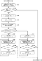
図3は、実施例1におけるスレーブストレージ(記憶装置B)のリビルド処理の手順を示すフローチャートである。図3の各ステップの処理は、CPU201による制御下でRAIDコントローラ251によって実行される。画像形成装置10が起動すると、RAIDコントローラ251は、図3の手順による処理を実行する。
<Procedure for rebuilding>
FIG. 3 is a flowchart showing a procedure for rebuilding the slave storage (storage device B) in the first embodiment. The processing of each step in FIG. 3 is executed by the
まず、RAIDコントローラ251は、S101で、記憶装置BとしてRAID部250部に新たに接続されたストレージを探索し、S102で、新しいストレージが記憶装置Bとして接続されたか否かを判定する。RAIDコントローラ251は、新たなストレージが接続されていない場合には(S102で「NO」)、図3の手順による処理を終了し、記憶装置Aを使用して動作するシングルモードへ移行する。一方、RAIDコントローラ251は、新たなストレージが接続された場合には(S102で「YES」)、処理をS103へ進める。
First, the
S103で、RAIDコントローラ251は、IDENTIFY DEVICEコマンドを記憶装置A及び記憶装置Bに対してそれぞれ発行する。これにより、RAIDコントローラ251は、IDENTIFY DEVICEコマンドに対する応答を各記憶装置から受信し、当該応答から各記憶装置の装置情報を取得する。装置情報には、例えば、対応する記憶装置における最大LBA値及び回転数情報が含まれる。
In S103, the
次にS104で、RAIDコントローラ251は、記憶装置Bのリビルド処理用に、記憶装置A及び記憶装置Bにそれぞれ対応する変数L_a,L_bを(状態保持部254に)作成する。変数L_a,L_bは、LBA値を保持するために使用される。また、S105で、RAIDコントローラ251は、記憶装置A及び記憶装置Bにそれぞれ対応する変数L_max_a,L_max_bを(状態保持部254に)作成する。更に、RAIDコントローラ251は、S103で取得した装置情報に基づいて、記憶装置Aの最大LBA値を、変数L_max_aに設定(代入)し、記憶装置Bの最大LBA値を、変数L_max_bに設定(代入)する。
Next, in S104, the
その後、S106で、RAIDコントローラ251は、S103で取得した装置情報に基づいて、記憶装置Bのタイプを判定する。例えば、装置情報に含まれる回転数情報が所定の回転数を示す場合には、記憶装置BはHDD(磁気ディスクで構成された第2タイプの記憶装置)であると判定できる。また、装置情報に含まれる回転数情報が回転しないメディアを示す場合には、記憶装置BはSSD(半導体メモリで構成された第1タイプの記憶装置)であると判定できる。RAIDコントローラ251は、記憶装置BがSSDであるか否かを判定し、記憶装置BがSSDである場合には(S106で「YES」)、S107へ処理を進め、記憶装置BがHDDである場合には(S106で「NO」)、S107へ処理を進める。
After that, in S106, the
なお、記憶装置Bのタイプは、記憶装置Bから当該記憶装置のSMART(Self Monitoring Analysis And Reporting Technology)情報を取得し、取得した情報に基づいて判定されてもよい。あるいは、記憶装置Bのタイプは、画像形成装置10に予め登録されている、記憶装置の型名又は型番等の情報に基づいて判定されてもよい。
The type of the storage device B may be determined by acquiring SMART (Self Monitoring Analysis And Reporting Technology) information of the storage device from the storage device B and based on the acquired information. Alternatively, the type of the storage device B may be determined based on information such as the model name or model number of the storage device registered in advance in the
(記憶装置BがSSDである場合)
記憶装置BがSSDである場合、S107で、RAIDコントローラ251は、変数L_a,L_bを以下のように更新し、処理をS108へ進める。
L_a=L_max_a
L_b=0
これにより、変数L_aには、記憶装置Aの最大LBA値が設定され、変数L_bには、記憶装置Bの最小LBA値(即ち、0)が設定される。最小LBA値は、各記憶装置の記憶領域における先頭部の領域に対応し、当該先頭部の領域に割り当てられたアドレスである。最大LBA値は、各記憶装置の記憶領域における最後部の領域に対応し、当該最後部の領域に割り当てられたアドレスである。
(When storage device B is SSD)
When the storage device B is an SSD, in S107, the
L_a = L_max_a
L_b = 0
As a result, the maximum LBA value of the storage device A is set in the variable L_a, and the minimum LBA value (that is, 0) of the storage device B is set in the variable L_b. The minimum LBA value corresponds to the region of the head portion in the storage area of each storage device, and is an address assigned to the region of the head portion. The maximum LBA value corresponds to the last area in the storage area of each storage device, and is an address assigned to the last area.
S108で、RAIDコントローラ251は、記憶装置Aにおける、変数L_a(LBA値)に対応する領域に格納されているデータを、記憶装置Bにおける、変数L_b(LBA値)に対応する領域にコピーする。このように、変数L_aは、記憶装置Aにおける、データのコピー元の領域に対応するLBA値を示し、変数L_bは、記憶装置Bにおける、データのコピー先の領域に対応するLBA値を示す。
In S108, the
その後、S109で、RAIDコントローラ251は、変数L_aが0と等しい(L_aが最小LBA値である)か否かを判定し、L_aが0と等しくない場合には、処理をS110へ進める。S110で、RAIDコントローラ251は、変数L_a,L_bを以下のように更新する。
L_a=L_a−1
L_b=L_b+1
即ち、RAIDコントローラ251は、変数L_aを1減少させ、変数L_bを1増加させる。この処理により、記憶装置Aにおけるコピー元の領域が、最大LBA値に対応する領域から、最小LBA値に対応する領域まで順に設定されることになる。また、記憶装置Bにおけるコピー先の領域が、最小LBA値に対応する領域から、最大LBA値に対応する領域まで順に設定されることになる。
After that, in S109, the
L_a = L_a-1
L_b =
That is, the
S110における変数L_a,L_bの更新後、RAIDコントローラ251は、処理をS108へ戻す。これにより、RAIDコントローラ251は、記憶装置A及び記憶装置Bにおける、変数L_a,L_bがそれぞれ示す次の領域を対象として、再び記憶装置Aから記憶装置Bへのデータのコピーを行う。RAIDコントローラ251は、このようにしてS108〜S110の処理を繰り返すことにより、記憶装置Aの記憶領域全体に格納されているデータを、記憶装置Bへコピーする。
After updating the variables L_a and L_b in S110, the
具体的には、RAIDコントローラ251は、記憶装置Aの記憶領域における最大LBA値に対応する領域(最後部の領域)から最小LBA値に対応する領域(先頭部の領域)まで順に、各領域に格納されているデータを読み出す。更に、RAIDコントローラ251は、記憶装置Aから順に読み出したデータを、記憶装置Bの記憶領域における最小LBA値に対応する領域(先頭部の領域)から最大LBA値に対応する領域(最後部の領域)まで順に書き込む。
Specifically, the
S109で、RAIDコントローラ251は、変数L_aが0と等しい場合(即ち、記憶装置Aにおける、最小LBA値に対応する領域に格納されているデータについての記憶装置Bへのコピーが完了した場合)、図3の手順による処理を終了する。その後、RAIDコントローラ251は、ミラーリングモードのミラーステートへ移行し、記憶装置A及び記憶装置B間におけるミラーリングを開始する。
In S109, the
なお、リビルド処理が完了すると、RAIDコントローラ251は、後述するアドレス変換テーブル(図5)を生成し、当該アドレス変換テーブルに基づいて、記憶装置Aに対して使用されるLBA値による記憶装置Bへのアクセス制御を行う。なお、アドレス変換テーブルは、同じデータが格納される記憶装置Aの領域と記憶装置Bの領域とにそれぞれ割り当てられたLBA値(アドレス)の対応関係を示す。このアドレス変換テーブルは、記憶装置Aに対して使用されるLBA値(アドレス)を、記憶装置Bに対して使用されるLBA値(アドレス)に変換するために用いられる。
When the rebuild process is completed, the
(記憶装置BがHDDである場合)
記憶装置BがHDDである場合、S111で、RAIDコントローラ251は、変数L_a,L_bを以下のように更新し、処理をS112へ進める。
L_a=0
L_b=0
これにより、変数L_aには、記憶装置Aの最小LBA値(即ち、0)が設定され、変数L_bには、記憶装置Bの最小LBA値(即ち、0)が設定される。S112で、RAIDコントローラ251は、S108と同様、記憶装置Aにおける、変数L_a(LBA値)に対応する領域に格納されているデータを、記憶装置Bにおける、変数L_b(LBA値)に対応する領域にコピーする。
(When the storage device B is an HDD)
When the storage device B is an HDD, in S111, the
L_a = 0
L_b = 0
As a result, the minimum LBA value (that is, 0) of the storage device A is set in the variable L_a, and the minimum LBA value (that is, 0) of the storage device B is set in the variable L_b. In S112, the
次にS113で、RAIDコントローラ251は、変数L_aがL_max_aと等しい(L_aが最大LBA値である)か否かを判定し、L_aがL_max_aと等しくない場合には、処理をS114へ進める。S114で、RAIDコントローラ251は、変数L_a,L_bを以下のように更新する。
L_a=L_a+1
L_b=L_b+1
即ち、RAIDコントローラ251は、変数L_aを1減少させ、変数L_bを1増加させる。この処理により、記憶装置Aにおけるコピー元の領域が、最小LBA値に対応する領域から、最大LBA値に対応する領域まで順に設定されることになる。また、記憶装置Bにおけるコピー先の領域が、最小LBA値に対応する領域から、最大LBA値に対応する領域まで順に設定されることになる。
Next, in S113, the
L_a =
L_b =
That is, the
S114における変数L_a,L_bの更新後、RAIDコントローラ251は、処理をS111へ戻す。これにより、RAIDコントローラ251は、記憶装置A及び記憶装置Bにおける、変数L_a,L_bがそれぞれ示す次の領域を対象として、再び記憶装置Aから記憶装置Bへのデータのコピーを行う。RAIDコントローラ251は、このようにしてS111〜S114の処理を繰り返すことにより、記憶装置Aの記憶領域全体に格納されているデータを、記憶装置Bへコピーする。
After updating the variables L_a and L_b in S114, the
具体的には、RAIDコントローラ251は、記憶装置BがSSDである場合とは逆に、記憶装置Aの記憶領域における最小LBA値に対応する領域から最大LBA値に対応する領域まで順に、各領域に格納されているデータを読み出す。更に、RAIDコントローラ251は、記憶装置Aから順に読み出したデータを、記憶装置Bの記憶領域における最小LBA値に対応する領域から最大LBA値に対応する領域まで順に書き込む。
Specifically, the
S113で、RAIDコントローラ251は、変数L_aがL_max_aと等しい場合(即ち、記憶装置Aにおける、最大LBA値に対応する領域に格納されているデータについての記憶装置Bへのコピーが完了した場合)、図3の手順による処理を終了する。その後、RAIDコントローラ251は、ミラーリングモードのミラーステートへ移行し、記憶装置A及び記憶装置B間におけるミラーリングを開始する。
In S113,
<リビルド処理の例>
図4(A)は、本実施例のリビルド処理における、記憶装置Aから記憶装置Bへのデータのコピーの例を示す概念図である。本例では、記憶装置AがHDD、記憶装置BがSSDである。
<Example of rebuild process>
FIG. 4A is a conceptual diagram showing an example of copying data from the storage device A to the storage device B in the rebuild process of this embodiment. In this example, the storage device A is an HDD and the storage device B is an SSD.
記憶装置Aとして使用されているHDDは、一般に、プラッタと称される円盤状の磁気ディスクを備え、当該ディスクがHDD内部で高速回転している。HDDでは、ディスクの外周部と内周部との間でデータ転送速度に差がある。ディスクの外周部は、内周部よりも円周が長いため、より多くのセクタを有し、内周部よりも高いデータ転送速度を有する。また、ディスクの外周部に対して小さいLBA値が割り当てられ(即ち、外周部が記憶領域の先頭部に対応する)、内周部に対して大きなLBA値が割り当てられる(即ち、内周部が記憶領域の最後部に対応する)。このため、記憶装置Aにおいて、システムの起動時間等に影響するシステムデータ(図4(A)では、起動データ及びシステム関連データ)は小さいLBA値に対応する領域に格納されることで、システム性能の向上が図られている。 The HDD used as the storage device A generally includes a disk-shaped magnetic disk called a platter, and the disk rotates at high speed inside the HDD. In an HDD, there is a difference in data transfer speed between the outer peripheral portion and the inner peripheral portion of the disk. Since the outer peripheral portion of the disk has a longer circumference than the inner peripheral portion, it has more sectors and has a higher data transfer rate than the inner peripheral portion. Further, a small LBA value is assigned to the outer peripheral portion of the disk (that is, the outer peripheral portion corresponds to the head portion of the storage area), and a large LBA value is assigned to the inner peripheral portion (that is, the inner peripheral portion is assigned). Corresponds to the end of the storage area). Therefore, in the storage device A, the system data that affects the system startup time and the like (in FIG. 4A, the startup data and the system-related data) are stored in the area corresponding to the small LBA value, so that the system performance Is being improved.
一方、記憶装置Bとして使用されているSSDは、磁気ディスクではなく半導体メモリで構成されている。このため、画像形成装置10の性能は、SSD内でシステムデータが格納される領域(即ち、LBA値)によらず一定である。本実施例のリビルド処理では、記憶装置Aから読み出されたデータは、記憶装置Bの記憶領域における最小LBA値に対応する領域から最大LBA値に対応する領域まで順に書き込まれる。
On the other hand, the SSD used as the storage device B is composed of a semiconductor memory instead of a magnetic disk. Therefore, the performance of the
記憶装置BとしてSSDが接続された場合、図4(A)に示すように、記憶装置Aの記憶領域における最大LBA値に対応する領域(最後部の領域)から最小LBA値に対応する領域(先頭部の領域)まで順に、各領域に格納されているデータが読み出される。記憶装置Aから順に読み出されたデータは、記憶装置Bの記憶領域における最小LBA値に対応する領域(先頭部の領域)から最大LBA値に対応する領域(最後部の領域)で順に書き込まれる。 When an SSD is connected as the storage device B, as shown in FIG. 4A, the area corresponding to the maximum LBA value (the rearmost area) in the storage area of the storage device A to the area corresponding to the minimum LBA value (the area corresponding to the minimum LBA value). The data stored in each area is read out in order up to the head area). The data read in order from the storage device A is written in order from the area corresponding to the minimum LBA value (the area at the beginning) to the area corresponding to the maximum LBA value (the area at the end) in the storage area of the storage device B. ..
このようなリビルド処理により、システムデータ(起動データ及びシステム関連データ)は、記憶装置Aから記憶装置Bへ最後にコピーされることになる。したがって、システムデータ以外のデータのコピーが行われている間のSSDの自己昇温により、SSDの温度が高くなった状態で、システムデータのコピーを行うことが可能になる。 By such a rebuild process, the system data (startup data and system-related data) is finally copied from the storage device A to the storage device B. Therefore, it is possible to copy the system data while the temperature of the SSD is high due to the self-heating of the SSD while the data other than the system data is being copied.
<アドレス変換テーブル>
上述のリビルド処理の結果、図4(A)に示すように、記憶装置Aと記憶装置Bとでパーティション構成が異なることになる。図5は、リビルド処理の完了後に用いられるアドレス変換テーブル(パーティションテーブル)である。CPU201は、図5に示す、ホストLBA値を用いて、記憶装置におけるアクセス対象の領域を指定する。ホストLBA値は、領域ごとに、記憶装置A(HDD)のLBA値と対応している一方、パーティション構成の相違に起因して、記憶装置B(SSD)のLBA値とは対応していない。このため、ホストLBA値を用いた記憶装置Bへのアクセスを実現するためには、RAID部250において、ホストLBA値から記憶装置BのLBA値へのLBA変換(アドレス変換)を行う必要がある。
<Address translation table>
As a result of the above-mentioned rebuild process, as shown in FIG. 4A, the partition configurations of the storage device A and the storage device B are different. FIG. 5 is an address translation table (partition table) used after the completion of the rebuild process. The
本実施例では、リビルド処理の完了後に、図5に示すアドレス変換テーブルが、RAIDコントローラ251によって生成される。生成されたアドレス変換テーブルは、状態保持部254によって保持され、CPU201から記憶装置へのアクセスが発生した際に、アドレス変換部253によるアドレス変換に使用される。RAIDコントローラ251は、アドレス変換部253によるアドレス変換テーブルを用いたアドレス変換に基づいて、ホストLBA値に対応するLBA値であり、かつ、記憶装置Aに対して使用されるLBA値による、記憶装置Bへのアクセス制御を行う。
In this embodiment, after the rebuild process is completed, the address translation table shown in FIG. 5 is generated by the
以上説明したように、本実施例では、SSDがリビルド処理の対象である場合、コピー元の記憶装置(HDD)における小さいLBA値に対応する領域(システム領域等)に格納されたシステムデータを、リビルド処理の終盤にコピー先(SSD)に書き込む。システムデータの書き込み(コピー)が開始される際には、SSDの温度が高くなっていることが期待される。即ち、SSDの温度が高い状態で、当該SSDに対してシステムデータが書き込まれることになる。これにより、SSDの温度が低い状態でシステムデータを書き込んだ場合よりも、書き込んだデータがSSDによって保持される期間(リテンション期間)を長くすることができる。したがって、例えば画像形成装置10において電源OFF状態が継続するような状況が生じても、短い期間でシステムデータがSSDから消失することを防止できる。
As described above, in this embodiment, when the SSD is the target of the rebuild process, the system data stored in the area (system area, etc.) corresponding to the small LBA value in the copy source storage device (HDD) is stored. Write to the copy destination (SSD) at the end of the rebuild process. It is expected that the temperature of the SSD will be high when the writing (copying) of the system data is started. That is, the system data is written to the SSD while the temperature of the SSD is high. As a result, the period (retention period) in which the written data is retained by the SSD can be made longer than when the system data is written in a state where the temperature of the SSD is low. Therefore, for example, even if a situation occurs in which the power-off state continues in the
[実施例2]
実施例2では、RAIDコントローラ251は、記憶装置BがSSDであれば、リビルド処理において、記憶装置Aから記憶装置Bへの全データのコピーを2回続けて行う。具体的には、RAIDコントローラ251は、記憶装置Aに格納された全データを記憶装置Bへコピーした後、記憶装置Aに格納された全データを記憶装置Bへ再度コピーする。即ち、記憶装置Aから記憶装置Bへの全データのコピーの間に、記憶装置B内のフラッシュメモリの温度が高くなった後に、システムデータが記憶装置Bへ再び書き込まれる。したがって、記憶装置Bによるシステムデータの保持期間を長くすることができる。以下では、実施例1と相違する点を中心として説明する。
[Example 2]
In the second embodiment, if the storage device B is an SSD, the
<リビルド処理の手順>
図6は、実施例2におけるスレーブストレージ(記憶装置B)のリビルド処理の手順を示すフローチャートである。図6の各ステップの処理は、CPU201による制御下でRAIDコントローラ251によって実行される。画像形成装置10が起動すると、RAIDコントローラ251は、図6の手順による処理を実行する。
<Procedure for rebuilding>
FIG. 6 is a flowchart showing a procedure for rebuilding the slave storage (storage device B) in the second embodiment. The processing of each step in FIG. 6 is executed by the
まず、S201及びS202は、実施例1のS101及びS102(図3)と同様である。S202で、RAIDコントローラ251は、新たなストレージが接続されていない場合には(S202で「NO」)、図6の手順による処理を終了し、記憶装置Aを使用して動作するシングルモードへ移行する。一方、RAIDコントローラ251は、新たなストレージが接続された場合には(S202で「YES」)、処理をS203へ進める。
First, S201 and S202 are the same as S101 and S102 (FIG. 3) of the first embodiment. In S202, the single-
S203で、RAIDコントローラ251は、記憶装置Bのタイプ(記憶装置BがSSDであるか否か)を判定し、記憶装置BがSSDである場合、S204へ処理を進め、記憶装置BがHDDである場合には、S205へ処理を進める。S204で、RAIDコントローラ251は、状態保持部254が保持しているコピーフラグをH(ハイ)に設定し、処理をS205へ進める。コピーフラグは、予めL(ロー)に設定されている。リビルド処理において、コピーフラグがHに設定されている場合には、記憶装置Aから記憶装置Bへの全データのコピーの完了後に、2回目のコピーを行うべきことを示す。
In S203, the
S205で、RAIDコントローラ251は、記憶装置Aの最小LBA値に対応する領域に格納されているデータから順に、記憶装置Bへのコピーを開始する。記憶装置Aから読み出されたデータは、記憶装置Bの最小LBA値に対応する領域から順に書き込まれる。その後、S206で、RAIDコントローラ251は、記憶装置Aから記憶装置Bへの全データのコピーが完了すると、S207へ処理を進める。
In S205, the
S207で、RAIDコントローラ251は、状態保持部254が保持しているコピーフラグがHに設定されているか否かを判定する。コピーフラグがHに設定されていない場合には、RAIDコントローラ251は、図6の手順による処理を終了し、ミラーリングモードのミラーステートへ移行し、記憶装置間でのミラーリングを開始する。一方、S207においてコピーフラグがHに設定されている場合には、RAIDコントローラ251は、処理をS208へ進める。
In S207, the
S208で、RAIDコントローラ251は、状態保持部254が保持しているコピーフラグをLに設定し、S205へ処理を戻す。S205及びS206では、RAIDコントローラ251は、再び、記憶装置Aから記憶装置Bへデータのコピーを行う。その後、S207で、RAIDコントローラ251は、コピーフラグがLに設定されているため、図6の手順による処理を終了し、ミラーステートへ移行して、記憶装置間でのミラーリングを開始する。このように、コピーフラグの設定により、記憶装置Aから記憶装置Bへのデータのコピーは2回に限定される。これにより、記憶装置B(SSD)への過剰な書き込み回数の増加、及びデータのコピーに伴う消費電力の増加を防ぐことができる。
In S208, the
以上説明したように、本実施例では、SSDがリビルド処理の対象である場合、コピー元の記憶装置からSSDへのデータのコピーを2回続けて行う。これにより、システムデータについての2回目のコピーが行われる際には、SSDの温度が高くなっていることが期待される。即ち、SSDの温度が高い状態で、当該SSDに対してシステムデータが書き込まれることになる。これにより、実施例1と同様、SSDによるシステムデータのリテンション期間を長くすることができ、例えば画像形成装置10において電源OFF状態が継続するような状況が生じても、短い期間でシステムデータがSSDから消失することを防止できる。
As described above, in this embodiment, when the SSD is the target of the rebuild process, the data is copied from the copy source storage device to the SSD twice in succession. As a result, it is expected that the temperature of the SSD will be high when the second copy of the system data is performed. That is, the system data is written to the SSD while the temperature of the SSD is high. As a result, as in the first embodiment, the retention period of the system data by the SSD can be lengthened, and even if a situation occurs in which the power off state continues in the
また、本実施例では、RAIDコントローラ251は、記憶装置Aと記憶装置Bとで、同じLBA値に対応する領域に同じデータが格納される。これにより、RAIDコントローラ251は、実施例1のようにアドレス変換テーブルを必要とすることなく、記憶装置Bへのアクセス制御を行うことが可能である。
Further, in the present embodiment, the
なお、本実施例は種々に変更することが可能である。例えば、上述の各処理を、RAIDコントローラ251ではなくCPU201が実行することも可能である。また、リビルド処理におけるSSDへの1回目のデータのコピーが完了した際に、RAIDコントローラ251は、記憶装置間でミラーリングを開始してもよい。これは、1回目のデータのコピーが完了した段階で、記憶装置間でミラーリングが開始できる状態になっているためである。これにより、2回のデータのコピーに起因してリビルド処理の完了までに要する時間が長くなる一方で、リビルド処理の完了前に、記憶装置間でのミラーリングを早期に開始することが可能になる。
In addition, this embodiment can be changed in various ways. For example, each of the above-mentioned processes can be executed by the
また、RAIDコントローラ251は、リビルド処理において、記憶装置Aに格納された全データを記憶装置Bへコピーした後、記憶装置Aに格納された全データではなく、システムデータのみを記憶装置Bへ再度コピーしてもよい。これにより、システムデータ以外の、比較的書き換え頻度が多いデータについては、2回目のデータのコピーを省略でき、2回目のデータのコピーをより短時間に完了することが可能である。また、システムデータ以外のデータのコピーに伴う、SSDへのデータの書き込み回数の増加を防ぐことが可能である。
Further, in the rebuild process, the
[実施例3]
実施例1及び2では、RAID部250によって記憶装置A及び記憶装置B間でRAID1を行われることで、CPU201は、記憶装置の構成を認識する必要なく、RAID部250を利用して記憶装置へアクセスできる。実施例3では、RAID部250ではなくCPU201がソフトウェアRAIDを行う場合の、記憶装置Bのリビルド処理について説明する。以下では、実施例1と相違する点を中心として説明する。
[Example 3]
In the first and second embodiments, the
<画像形成装置>
図7は、本実施例における画像形成装置10の概略的なハードウェア構成例を示すブロック図である。図7に示すように、本実施例の画像形成装置10は、コントローラ部200にRAID部250が設けられていない点で、実施例1(図1(A))と異なる。このため、本実施例では、CPU201は、システムバス210を介して、記憶装置A(208)及び記憶装置B(209)へ直接アクセスする。
<Image forming device>
FIG. 7 is a block diagram showing a schematic hardware configuration example of the
<リビルド処理の手順>
本実施例では、CPU201は、記憶装置BがSSDであれば、リビルド処理において、記憶装置Aの記憶領域における最後部の領域から先頭部の領域まで順に、各領域に格納されているデータを記憶装置Bへコピーする。これにより、記憶装置Aに格納されたデータのうちで、記憶装置Aの記憶領域における先頭部の領域に格納されたシステムデータが最後にコピーされる。したがって、記憶装置B内のフラッシュメモリの温度が高くなってから、システムデータを記憶装置Bへコピーすることが可能になる。
<Procedure for rebuilding>
In this embodiment, if the storage device B is an SSD, the
図8は、実施例3におけるスレーブストレージ(記憶装置B)のリビルド処理の手順を示すフローチャートである。図8の各ステップの処理は、CPU201によって実行される。CPU201は、ROM203に格納された制御プログラムをRAM202に展開して実行することにより、各ステップの処理を実現しうる。本実施例では、画像形成装置10が起動すると、CPU201は、図8の手順による処理を実行する。
FIG. 8 is a flowchart showing a procedure for rebuilding the slave storage (storage device B) in the third embodiment. The processing of each step in FIG. 8 is executed by the
まず、S301及びS302は、RAIDコントローラ251ではなくCPU201が処理を実行する点を除き、実施例1のS101及びS102(図3)と同様である。S302で、CPU201は、新たなストレージが接続されていない場合には(S302で「NO」)、図8の手順による処理を終了し、記憶装置Aを使用して動作するシングルモードへ移行する。一方、CPU201は、新たなストレージが接続された場合には(S302で「YES」)、処理をS303へ進める。
First, S301 and S302 are the same as S101 and S102 (FIG. 3) of the first embodiment except that the
S303で、CPU201は、記憶装置Bのタイプ(記憶装置BがSSDであるか否か)を判定し、記憶装置BがSSDである場合、S304へ処理を進め、記憶装置BがHDDである場合には、S305へ処理を進める。S304で、CPU201は、記憶装置Aの最大LBA値に対応する領域に格納されているデータから順に、記憶装置Bへのコピーを開始し、S306へ処理を進める。一方、S305で、CPU201は、記憶装置Aの最小LBA値に対応する領域に格納されているデータから順に、記憶装置Bへのコピーを開始し、S306へ処理を進める。S306で、CPU201は、記憶装置Aから記憶装置Bへの全データのコピーが完了すると、図8の手順による処理を終了し、ミラーリングモードのミラーステートへ移行し、記憶装置間でのミラーリングを開始する。
In S303, the
<リビルド処理の例>
図4(B)は、本実施例のリビルド処理における、記憶装置Aから記憶装置Bへのデータのコピーの例を示す概念図である。本例では、記憶装置AがHDD、記憶装置BがSSDである。本実施例では、記憶装置BとしてSSDが接続された場合、記憶装置Aの記憶領域における最大LBA値に対応する領域(最後部の領域)から最小LBA値に対応する領域(先頭部の領域)まで順に、各領域に格納されているデータが読み出される。記憶装置Aから順に読み出されたデータは、記憶装置Bの記憶領域における最大LBA値に対応する領域(最後部の領域)から最小LBA値に対応する領域(先頭部の領域)で順に書き込まれる。
<Example of rebuild process>
FIG. 4B is a conceptual diagram showing an example of copying data from the storage device A to the storage device B in the rebuild process of this embodiment. In this example, the storage device A is an HDD and the storage device B is an SSD. In this embodiment, when an SSD is connected as the storage device B, the area corresponding to the maximum LBA value (the last area) to the area corresponding to the minimum LBA value (the area at the beginning) in the storage area of the storage device A. The data stored in each area is read out in order up to. The data read in order from the storage device A is written in order from the area corresponding to the maximum LBA value (the last area) to the area corresponding to the minimum LBA value (the area at the beginning) in the storage area of the storage device B. ..
以上説明したように、本実施例では、実施例1と同様、SSDがリビルド処理の対象である場合、コピー元の記憶装置における小さいLBA値に対応する領域に格納されたシステムデータを、リビルド処理の終盤にコピー先(SSD)に書き込む。これにより、CPU201がソフトウェアRAIDを実行する場合においても、SSDによるシステムデータのリテンション期間を長くすることができる。また、例えば画像形成装置10において電源OFF状態が継続するような状況が生じても、短い期間でシステムデータがSSDから消失することを防止できる。
As described above, in the present embodiment, as in the first embodiment, when the SSD is the target of the rebuild process, the system data stored in the area corresponding to the small LBA value in the copy source storage device is subjected to the rebuild process. Write to the copy destination (SSD) at the end of. As a result, even when the
[実施例4]
実施例4では、実施例3と同様、RAID部250ではなくCPU201がソフトウェアRAIDを行う場合の、記憶装置Bのリビルド処理について説明する。以下では、実施例1と相違する点を中心として説明する。
[Example 4]
In the fourth embodiment, as in the third embodiment, the rebuild process of the storage device B when the
本実施例における画像形成装置10は、実施例3と同様、RAID部250が存在しない、図7に示される構成を有する。このため、CPU201は、システムバス210を介して、記憶装置A(208)及び記憶装置B(209)へ直接アクセスする。RAID部250が存在しない場合には、実施例1のリビルド処理(図3)は、RAIDコントローラ251ではなく、CPU201によって実行することが可能である。
Similar to the third embodiment, the
本実施例のリビルド処理の手順は、実施例1(図3)と同様である。ただし、本実施例は、各ステップの処理は、RAIDコントローラ251ではなく、CPU201によって実行される。この場合、変数L_a,L_b,L_max_a,L_max_bについては、例えば、各変数に対応する記憶領域がRAM202に確保される。
The procedure for the rebuilding process of this embodiment is the same as that of the first embodiment (FIG. 3). However, in this embodiment, the processing of each step is executed not by the
本実施例において、記憶装置AにHDD、記憶装置BにSSDが接続された場合のパーティション構成例は、実施例1(図4(A))と同様である。本実施例は、RAIDコントローラ251の処理をCPU201が行う点のみが差異であるため、構成されるパーティションは実施例1と変わらない。また、本実施例において、リビルドが完了した後に用いられるアドレス変換テーブルは、実施例1(図5)と同様である。この場合、CPU201は、生成したアドレス変換テーブルを、不揮発性メモリであるROM203に保持しうる。CPU201は、画像形成装置10の起動後に、ROM203からアドレス変換テーブルをRAM202に展開し、当該アドレス変換テーブルに基づいて、記憶装置Bへのアクセス制御を行う。
In this embodiment, the partition configuration example when the HDD is connected to the storage device A and the SSD is connected to the storage device B is the same as that of the first embodiment (FIG. 4 (A)). In this embodiment, the only difference is that the
本実施例では、実施例1と同様、SSDがリビルド処理の対象である場合、コピー元の記憶装置における小さいLBA値に対応する領域に格納されたシステムデータを、リビルド処理の終盤にコピー先(SSD)に書き込む。これにより、CPU201がソフトウェアRAIDを実行する場合においても、SSDによるシステムデータのリテンション期間を長くすることができる。また、例えば画像形成装置10において電源OFF状態が継続するような状況が生じても、短い期間でシステムデータがSSDから消失することを防止できる。
In this embodiment, as in the first embodiment, when the SSD is the target of the rebuild process, the system data stored in the area corresponding to the small LBA value in the copy source storage device is copied to the copy destination (at the end of the rebuild process). Write to SSD). As a result, even when the
[その他の実施形態]
本発明は、上述の実施形態の1以上の機能を実現するプログラムを、ネットワーク又は記憶媒体を介してシステム又は装置に供給し、そのシステム又は装置のコンピュータにおける1つ以上のプロセッサーがプログラムを読出し実行する処理でも実現可能である。また、1以上の機能を実現する回路(例えば、ASIC)によっても実現可能である。
[Other Embodiments]
The present invention supplies a program that realizes one or more functions of the above-described embodiment to a system or device via a network or storage medium, and one or more processors in the computer of the system or device reads and executes the program. It can also be realized by the processing to be performed. It can also be realized by a circuit (for example, ASIC) that realizes one or more functions.
10:画像形成装置、201:CPU、202:RAM、203:ROM、204:LANコントローラ、205:電源制御部、206:画像処理部、208:記憶装置A、209:記憶装置B、250:RAID部、251:RAIDコントローラ、252:フォーマット管理部、253:アドレス変換部、254:状態保持部 10: Image forming device, 201: CPU, 202: RAM, 203: ROM, 204: LAN controller, 205: Power supply control unit, 206: Image processing unit, 208: Storage device A, 209: Storage device B, 250: RAID Unit, 251: RAID controller, 252: Format management unit, 253: Address conversion unit, 254: State holding unit
Claims (10)
前記情報処理装置の起動に用いるシステムデータが記憶領域の先頭部の領域に格納された第1記憶装置と、
前記第1記憶装置との間でデータのミラーリングが行われる第2記憶装置と、
前記第1記憶装置に格納されたデータを前記第2記憶装置にコピーすることによって前記第2記憶装置のリビルド処理を行う制御手段と、を備え、
前記制御手段は、前記第2記憶装置が半導体メモリで構成された第1タイプの記憶装置であれば、前記リビルド処理において、前記第1記憶装置に格納されたデータのうち、前記システムデータ以外のデータを前記第2記憶装置にコピーした後に、前記システムデータを前記第2記憶装置へコピーし、
前記制御手段は、前記第2記憶装置が磁気ディスクで構成された第2タイプの記憶装置であれば、前記第1記憶装置の記憶領域の前記先頭部の領域から最後部の領域まで順に、各領域に格納されているデータを読み出し、前記第1記憶装置から順に読み出したデータを、前記第2記憶装置の記憶領域における前記先頭部の領域から前記最後部の領域まで順に書き込む
ことを特徴とする情報処理装置。 It is an information processing device
The first storage device in which the system data used for activating the information processing device is stored in the head area of the storage area, and
A second storage device in which data is mirrored to and from the first storage device,
A control means for performing a rebuild process of the second storage device by copying the data stored in the first storage device to the second storage device is provided.
Wherein, if the first type of storage device in which the second storage device is a semiconductor memory, in the rebuild process, among the data stored in the first storage device, other than the system data After copying the data to the second storage device, the system data is copied to the second storage device.
If the second storage device is a second type storage device composed of a magnetic disk, the control means is in order from the head region to the last region of the storage area of the first storage device. The data stored in the area is read out, and the data read out in order from the first storage device is sequentially written from the head area to the last area in the storage area of the second storage device. Information processing device.
ことを特徴とする請求項1に記載の情報処理装置。 Before SL control means, if said second storage device the storage device of the first type, in order from the region of the end portion in the storage area of the first storage device to the area of the head portion, stored in each area The information processing device according to claim 1, wherein the data is copied to the second storage device.
前記第1記憶装置の記憶領域における前記最後部の領域から前記先頭部の領域まで順に、各領域に格納されているデータを読み出し、
前記第1記憶装置から順に読み出したデータを、前記第2記憶装置の記憶領域における前記先頭部の領域から前記最後部の領域まで順に書き込む
ことを特徴とする請求項2に記載の情報処理装置。 If the second storage device is the first type storage device, the control means may be used.
The data stored in each area is read out in order from the last area to the first area in the storage area of the first storage device.
The information processing apparatus according to claim 2, wherein the data read in order from the first storage device is sequentially written from the head region to the last region in the storage area of the second storage device.
前記リビルド処理が完了した後に、同じデータが格納される前記第1記憶装置の領域と前記第2記憶装置の領域とにそれぞれ割り当てられたアドレスの対応関係を示し、前記第1記憶装置に対して使用されるアドレスを、前記第2記憶装置に対して使用されるアドレスに変換するための変換テーブルを生成し、
前記変換テーブルに基づいて、前記第1記憶装置に対して使用されるアドレスによる前記第2記憶装置へのアクセス制御を行う
ことを特徴とする請求項3に記載の情報処理装置。 The control means
After the rebuild process is completed, the correspondence between the addresses assigned to the area of the first storage device and the area of the second storage device in which the same data is stored is shown, and the correspondence relationship between the first storage device and the first storage device is shown. Generate a translation table for translating the used address to the address used for the second storage device.
The information processing device according to claim 3, wherein access control to the second storage device is performed by an address used for the first storage device based on the conversion table.
前記第1記憶装置の記憶領域における前記最後部の領域から前記先頭部の領域まで順に、各領域に格納されているデータを読み出し、
前記第1記憶装置から順に読み出したデータを、前記第2記憶装置の記憶領域における前記最後部の領域から前記先頭部の領域まで順に書き込む
ことを特徴とする請求項2に記載の情報処理装置。 If the second storage device is the first type storage device, the control means may be used.
The data stored in each area is read out in order from the last area to the first area in the storage area of the first storage device.
The information processing apparatus according to claim 2, wherein the data read in order from the first storage device is sequentially written from the last region to the head region in the storage area of the second storage device.
ことを特徴とする請求項1に記載の情報処理装置。 If the second storage device is the first type storage device, the control means copies all the data stored in the first storage device to the second storage device, and then stores the data in the first storage device. The information processing device according to claim 1, wherein all the stored data is copied again to the second storage device.
ことを特徴とする請求項1に記載の情報処理装置。 If the second storage device is the first type storage device, the control means copies all the data stored in the first storage device to the second storage device, and then stores the data in the first storage device. The information processing device according to claim 1, wherein the stored system data is copied again to the second storage device.
ことを特徴とする請求項1から7のいずれか1項に記載の情報処理装置。 Or wherein the control unit obtains the device information from the second storage device, based on the device information, which is the second storage device the storage device of the second type or a storage device of the first type The information processing apparatus according to any one of claims 1 to 7 , wherein the information processing apparatus is determined.
前記第1記憶装置に格納されたデータを前記第2記憶装置にコピーすることによって前記第2記憶装置のリビルド処理を行う制御工程を有し、
前記制御工程では、前記第2記憶装置が半導体メモリで構成された第1タイプの記憶装置であれば、前記リビルド処理において、前記第1記憶装置に格納されたデータのうち、前記システムデータ以外のデータを前記第2記憶装置にコピーした後に、前記システムデータを前記第2記憶装置へコピーし、
前記制御工程では、前記第2記憶装置が磁気ディスクで構成された第2タイプの記憶装置であれば、前記第1記憶装置の記憶領域の前記先頭部の領域から最後部の領域まで順に、各領域に格納されているデータを読み出し、前記第1記憶装置から順に読み出したデータを、前記第2記憶装置の記憶領域における前記先頭部の領域から前記最後部の領域まで順に書き込む
ことを特徴とする情報処理装置の制御方法。 It includes a first storage device in which system data used for activating an information processing device is stored in an area at the beginning of a storage area, and a second storage device in which data is mirrored between the first storage device. It is a control method for information processing equipment.
It has a control step of performing a rebuild process of the second storage device by copying the data stored in the first storage device to the second storage device.
In the control step, if the first type of storage device in which the second storage device is a semiconductor memory, in the rebuild process, among the data stored in the first storage device, other than the system data After copying the data to the second storage device, the system data is copied to the second storage device.
In the control step, if the second storage device is a second type storage device composed of a magnetic disk, each of the storage areas of the first storage device is in order from the head region to the last region. The data stored in the area is read out, and the data read out in order from the first storage device is sequentially written from the head area to the last area in the storage area of the second storage device. Information processing device control method.
Priority Applications (2)
| Application Number | Priority Date | Filing Date | Title |
|---|---|---|---|
| JP2017136439A JP6924088B2 (en) | 2017-07-12 | 2017-07-12 | Information processing equipment, its control method, and programs |
| US16/030,133 US10853205B2 (en) | 2017-07-12 | 2018-07-09 | Information processing apparatus, method of controlling the same and storage medium |
Applications Claiming Priority (1)
| Application Number | Priority Date | Filing Date | Title |
|---|---|---|---|
| JP2017136439A JP6924088B2 (en) | 2017-07-12 | 2017-07-12 | Information processing equipment, its control method, and programs |
Publications (3)
| Publication Number | Publication Date |
|---|---|
| JP2019020846A JP2019020846A (en) | 2019-02-07 |
| JP2019020846A5 JP2019020846A5 (en) | 2020-08-06 |
| JP6924088B2 true JP6924088B2 (en) | 2021-08-25 |
Family
ID=65000653
Family Applications (1)
| Application Number | Title | Priority Date | Filing Date |
|---|---|---|---|
| JP2017136439A Active JP6924088B2 (en) | 2017-07-12 | 2017-07-12 | Information processing equipment, its control method, and programs |
Country Status (2)
| Country | Link |
|---|---|
| US (1) | US10853205B2 (en) |
| JP (1) | JP6924088B2 (en) |
Family Cites Families (13)
| Publication number | Priority date | Publication date | Assignee | Title |
|---|---|---|---|---|
| JPH01292421A (en) * | 1988-05-19 | 1989-11-24 | Mitsubishi Electric Corp | Method for copying data in memory card |
| ES2169575T3 (en) * | 1999-04-10 | 2002-07-01 | Basis Gmbh Edv Vertriebs Ges | DATA SUPPORT WITH A FUNDAMENTAL STATE REPRODUCIBLE OF BASIC DATA AND PROCEDURE FOR THEIR REALIZATION. |
| JP2001282261A (en) | 2000-03-30 | 2001-10-12 | Canon Inc | Speech data setting device and method, speech data forming device and method, recording medium |
| US7000145B2 (en) * | 2003-06-18 | 2006-02-14 | International Business Machines Corporation | Method, system, and program for reverse restore of an incremental virtual copy |
| JP4888935B2 (en) | 2005-03-14 | 2012-02-29 | 株式会社リコー | Storage system |
| US8024547B2 (en) * | 2007-05-01 | 2011-09-20 | Vivante Corporation | Virtual memory translation with pre-fetch prediction |
| JP2012079100A (en) | 2010-10-01 | 2012-04-19 | Canon Inc | Disk control apparatus and method and program |
| JP5742362B2 (en) * | 2011-03-28 | 2015-07-01 | 富士通株式会社 | Evacuation processing device |
| JP5941273B2 (en) | 2011-12-02 | 2016-06-29 | キヤノン株式会社 | Information processing apparatus and control method thereof |
| JP2014016892A (en) * | 2012-07-10 | 2014-01-30 | Nec Corp | Semiconductor memory device and method of controlling the same |
| GB2514810A (en) * | 2013-06-05 | 2014-12-10 | Ibm | Rebuilding data of a storage system |
| JP6399755B2 (en) * | 2014-01-06 | 2018-10-03 | キヤノン株式会社 | Mirroring apparatus and control method thereof |
| US10198326B2 (en) * | 2017-03-09 | 2019-02-05 | Apple Inc. | Intelligent restoration of a computing device |
-
2017
- 2017-07-12 JP JP2017136439A patent/JP6924088B2/en active Active
-
2018
- 2018-07-09 US US16/030,133 patent/US10853205B2/en active Active
Also Published As
| Publication number | Publication date |
|---|---|
| US10853205B2 (en) | 2020-12-01 |
| JP2019020846A (en) | 2019-02-07 |
| US20190018745A1 (en) | 2019-01-17 |
Similar Documents
| Publication | Publication Date | Title |
|---|---|---|
| US8291155B2 (en) | Data access method, memory controller and memory storage system | |
| JP5220747B2 (en) | Nonvolatile storage device and nonvolatile storage system | |
| JP4828816B2 (en) | Memory card, semiconductor device, and memory card control method | |
| JP4884041B2 (en) | Storage system for issuing optimum I / O command to automatically expandable volume and control method thereof | |
| JP5721344B2 (en) | System, system control method, and program | |
| KR20100110652A (en) | Memory apparatus and method for updating firmware of the memory apparatus | |
| JP2009116873A (en) | Solid state memory (ssm), computer system having ssm, and ssm driving method | |
| US9223695B2 (en) | Information processing apparatus | |
| KR20070024504A (en) | Storage device, memory management method and program | |
| JP2005010897A (en) | Computer system, computer system starting method and program | |
| JP2014126989A (en) | Control device, control method, and program | |
| JP2011028430A (en) | Information processing apparatus, control method for information processing apparatus, and program | |
| JP2014010498A5 (en) | ||
| US20130013885A1 (en) | Memory storage device, memory controller, and method for identifying valid data | |
| JP4843222B2 (en) | Semiconductor memory device control method, memory card, and host device | |
| JP2020086535A (en) | Memory controller and memory system | |
| JP2007011872A (en) | Memory card and control method therefor | |
| JP5668163B2 (en) | Information processing device | |
| JP4242245B2 (en) | Flash ROM control device | |
| JP2006011533A (en) | Memory card, semiconductor device, and control method of semiconductor memory | |
| JP6924088B2 (en) | Information processing equipment, its control method, and programs | |
| KR102123701B1 (en) | Network boot system | |
| JP2005115562A (en) | Flash rom controller | |
| JP2000030375A (en) | Data processing system, access device, and recording media | |
| WO2020039927A1 (en) | Non-volatile storage device, host device, and data storage system |
Legal Events
| Date | Code | Title | Description |
|---|---|---|---|
| A521 | Request for written amendment filed |
Free format text: JAPANESE INTERMEDIATE CODE: A523 Effective date: 20200623 |
|
| A621 | Written request for application examination |
Free format text: JAPANESE INTERMEDIATE CODE: A621 Effective date: 20200623 |
|
| RD01 | Notification of change of attorney |
Free format text: JAPANESE INTERMEDIATE CODE: A7421 Effective date: 20210103 |
|
| A521 | Request for written amendment filed |
Free format text: JAPANESE INTERMEDIATE CODE: A523 Effective date: 20210113 |
|
| A977 | Report on retrieval |
Free format text: JAPANESE INTERMEDIATE CODE: A971007 Effective date: 20210324 |
|
| A131 | Notification of reasons for refusal |
Free format text: JAPANESE INTERMEDIATE CODE: A131 Effective date: 20210402 |
|
| A521 | Request for written amendment filed |
Free format text: JAPANESE INTERMEDIATE CODE: A523 Effective date: 20210531 |
|
| TRDD | Decision of grant or rejection written | ||
| A01 | Written decision to grant a patent or to grant a registration (utility model) |
Free format text: JAPANESE INTERMEDIATE CODE: A01 Effective date: 20210702 |
|
| A61 | First payment of annual fees (during grant procedure) |
Free format text: JAPANESE INTERMEDIATE CODE: A61 Effective date: 20210730 |
|
| R151 | Written notification of patent or utility model registration |
Ref document number: 6924088 Country of ref document: JP Free format text: JAPANESE INTERMEDIATE CODE: R151 |