JP6918552B2 - Read-out control circuit, solid-state image sensor, and how to drive the image sensor - Google Patents
Read-out control circuit, solid-state image sensor, and how to drive the image sensor Download PDFInfo
- Publication number
- JP6918552B2 JP6918552B2 JP2017075320A JP2017075320A JP6918552B2 JP 6918552 B2 JP6918552 B2 JP 6918552B2 JP 2017075320 A JP2017075320 A JP 2017075320A JP 2017075320 A JP2017075320 A JP 2017075320A JP 6918552 B2 JP6918552 B2 JP 6918552B2
- Authority
- JP
- Japan
- Prior art keywords
- diffusion capacitance
- signal
- pixel
- floating diffusion
- capacitance means
- Prior art date
- Legal status (The legal status is an assumption and is not a legal conclusion. Google has not performed a legal analysis and makes no representation as to the accuracy of the status listed.)
- Active
Links
Images


Landscapes
- Solid State Image Pick-Up Elements (AREA)
- Transforming Light Signals Into Electric Signals (AREA)
Description
本発明は、読出し制御回路、固体撮像素子、および撮像素子の駆動方法に関し、詳しくは、光電変換部により得られた光電子に基づく、感度が異なる複数の信号を、この後の信号処理部で合成され得るように出力する、読出し制御回路、固体撮像素子、および撮像素子の駆動方法に関するものである。 The present invention relates to a readout control circuit, a solid-state image sensor, and a method for driving the image sensor. Specifically, a plurality of signals having different sensitivities based on photoelectrons obtained by a photoelectric conversion unit are synthesized by a subsequent signal processing unit. It relates to a read-out control circuit, a solid-state image sensor, and a method of driving the image sensor, which are output so as to be possible.
従来、固体撮像素子、例えばCMOSイメージセンサにおいては、光電変換によって単位画素に蓄積された信号電荷の値に応じて、略線形な出力信号が得られるので、光電変換部の飽和信号量と暗時雑音の比からダイナミックレンジが決まってしまう。 Conventionally, in a solid-state image sensor, for example, a CMOS image sensor, a substantially linear output signal can be obtained according to the value of the signal charge accumulated in a unit pixel by photoelectric conversion. The dynamic range is determined by the noise ratio.
このような固体撮像素子では、低輝度の被写体にカメラレンズの絞りを合わせると高輝度の被写体の信号は飽和してしまい、逆に高輝度の被写体にカメラレンズの絞りを合わせると低輝度の被写体の信号は雑音に埋もれてしまうことから、高輝度、低輝度のいずれであっても良好な画像が得られる、十分に広いダイナミックレンジを有する画像素子が求められていた。 With such a solid-state image sensor, if the aperture of the camera lens is adjusted to a low-brightness subject, the signal of the high-brightness subject will be saturated. Since the signal of the above is buried in noise, there has been a demand for an image sensor having a sufficiently wide dynamic range, which can obtain a good image regardless of whether the brightness is high or low.
そして、単にダイナミックレンジを拡大するだけではなく、次の(1)〜(4)のような項目を満たした上でダイナミックレンジを拡大化することが求められていた。すなわち、(1)光電変換部を分割しないで解像度特性を優れたものとすることができること、(2)露光時間を分割しないで動画撮像特性を優れたものとし得ること、(3)高感度、高S/N化と広ダイナミックレンジ化のトレードオフを解消できること、および(4)超多画素において
高フレーム周波数を読み出すことができること、が求められていた。
Then, it was required not only to expand the dynamic range but also to expand the dynamic range after satisfying the following items (1) to (4). That is, (1) the resolution characteristics can be made excellent without dividing the photoelectric conversion unit, (2) the moving image imaging characteristics can be made excellent without dividing the exposure time, (3) high sensitivity, It has been required that the trade-off between high S / N and wide dynamic range can be eliminated, and (4) high frame frequency can be read out with an ultra-multi-pixel.
ここで、入射光量に対する、出力信号量のダイナミックレンジを拡大するために、同一の画素から長時間露光と短時間露光により得られた2つの信号を複数回読み出し、読み出された感度が異なる複数の信号を、撮像素子の後段の信号処理部で合成する方法が知られている(特許文献1、非特許文献1を参照)。
Here, in order to expand the dynamic range of the output signal amount with respect to the incident light amount, two signals obtained by long-time exposure and short-time exposure are read multiple times from the same pixel, and the read sensitivities are different. There is known a method of synthesizing the signals of the above in the signal processing unit in the subsequent stage of the image pickup device (see
また、図22に示す従来技術においては、各画素は、光を受光して光電荷を生成するフォトダイオードPDと、このPDに隣接して設けられた光電荷を転送する転送トランジスタTと、このTを介して上記PDに接続して設けられたフローティングディフュージョンFDと、露光蓄積動作時に上記PDから溢れ出た光電荷を上記Tを通じて蓄積する第1の蓄積容量CSaおよび第2の蓄積容量CSbと、を備える。さらに、これらの蓄積容量CSa、CSbの他、上記FD内の信号電荷を排出するためのリセットトランジスタRと、上記FDと上記CSaの間に設けられた第1の蓄積トランジスタCaと、上記CSaと上記CSbの間に設けられた第2の蓄積トランジスタCbと、上記FDと上記CSaと上記CSbの信号電荷を電圧として読み出すための増幅トランジスタSFと、このSFに接続して設けられ画素ないしは画素ブロックを選択するための選択トランジスタXとを備えている。 Further, in the prior art shown in FIG. 22, each pixel has a photodiode PD that receives light and generates an optical charge, a transfer transistor T that is provided adjacent to the PD and transfers an optical charge, and the transfer transistor T. A floating diffusion FD provided by connecting to the PD via the T, and a first storage capacity CSa and a second storage capacity CSb that store the light charge overflowing from the PD during the exposure storage operation through the T. , Equipped with. Further, in addition to these storage capacities CSa and CSb, a reset transistor R for discharging the signal charge in the FD, a first storage transistor Ca provided between the FD and the CSa, and the CSa A second storage transistor Cb provided between the CSb, an amplification transistor SF for reading the signal charges of the FD, the CSa, and the CSb as a voltage, and a pixel or a pixel block provided connected to the SF. It is provided with a selection transistor X for selecting.
このように構成された従来技術は、上記の構成の画素が2次元または1次元のアレイ状に複数個集積されており、各画素において、転送トランジスタT、第1の蓄積トランジスタCa、第2の蓄積トランジスタCb、リセットトランジスタRのゲート電極に、各駆動ラインが接続され、また、選択トランジスタXのゲート電極には行シフトレジスタから駆動される画素選択ラインが接続され、さらに、選択トランジスタXの出力側ソースに1つの出力ラインOUTが接続され、列シフトレジスタにより制御されて、いずれの信号もこ
の1つの出力ラインOUTを通して出力される(特許文献2を参照)。
しかしながら、上記特許文献1等に記載の従来技術では、長時間露光と短時間露光によ
る信号を合成する方法では、信号量は2倍にならないのに対して、読出しのノイズは各々が積算されて2倍となることから、特に低照度においてはS/Nが劣化する。
また、長時間露光と短時間露光は互いに異なるタイミングで撮像するので、撮像時刻にずれが生じ、高速に動く被写体が互いにずれて見えるという問題が生じる。また、一画素あたりの読み出し回数が複数回になるので、最高フレーム周波数が低下する。
However, in the conventional technique described in
Further, since the long-time exposure and the short-time exposure are imaged at different timings, there is a problem that the imaging times are deviated and the subjects moving at high speed appear to be deviated from each other. Further, since the number of readings per pixel is a plurality of times, the maximum frame frequency is lowered.
また、上記特許文献2に記載の従来技術では、蓄積容量素子を使用し飽和前信号と過飽和信号を読み出す手法であり、一画素あたりの読み出し回数が複数回となるので、最高フレーム周波数が低下する。
Further, in the prior art described in
本発明は上記の事情に鑑みなされたものであり、優れた動画撮像特性と解像度特性を実現し得、低照度において飽和レベルを狭めることなく線形かつ高S/Nの信号取得を可能にするとともに、高照度においては線形領域での良好なS/Nを可能にすることができ、ダイナミックレンジの拡大を図ることができるとともに最高フレーム周波数の低下を抑制し得る、読出し制御回路、固体撮像素子、および撮像素子の駆動方法を提供することを目的とするものである。 The present invention has been made in view of the above circumstances, can realize excellent moving image imaging characteristics and resolution characteristics, and enables linear and high S / N signal acquisition without narrowing the saturation level in low illuminance. , Read control circuit, solid-state image sensor, which can enable good S / N in the linear region in high illuminance, can expand the dynamic range, and can suppress the decrease of the maximum frame frequency. An object of the present invention is to provide a method for driving an image pickup device.
本発明の、読出し制御回路は、
固体撮像装置の読出し制御回路において、光電変換部からの信号が蓄積される、容量値が相対的に小さく変換ゲインが大きい第1の浮遊拡散容量手段と、
該第1の浮遊拡散容量手段からの信号がオーバーフローゲートを経て入力され蓄積される、容量値が相対的に大きく変換ゲインが小さい第2の浮遊拡散容量手段とを備え、
該第1の浮遊拡散容量手段と該第2の浮遊拡散容量手段は、ともに、固有の画素出力回路を備え、前記第1および第2の浮遊拡散容量手段各々に係る前記画素出力回路は互いに並列に配置されており、該画素出力回路の各々からは、各水平走査(H)ライン毎に、同時に画素出力信号が出力されるように構成され、
前記光電変換部への入射光に対する、前記第1および第2の浮遊拡散容量手段各々に係る前記画素出力回路からの各前記画素出力信号を合成した合成後出力信号の傾きが、前記入射光が低強度側から高強度側に至る領域で大から小に変化する構成とされていることを特徴とするものである。
また、前記第1の浮遊拡散容量手段につき、転送トランジスタを含む4つのトランジスタを用いることにより、および前記第2の浮遊拡散容量手段につき、オーバーフローゲートを含む4つのトランジスタを用いることにより、各々構成することができる。
また、前記第1の浮遊拡散容量手段につき、転送トランジスタを含まない3つのトランジスタを用いることにより、および前記第2の浮遊拡散容量手段につき、オーバーフローゲートを含む4つのトランジスタを用いることにより、各々構成することができる。この場合において、前記光電変換部が光電変換膜から構成されていることが好ましい。
The read control circuit of the present invention
In the read-out control circuit of the solid-state image sensor, the first floating diffusion capacitance means in which the signal from the photoelectric conversion unit is accumulated, the capacitance value is relatively small, and the conversion gain is large,
A second floating diffusion capacitance means having a relatively large capacitance value and a small conversion gain, in which a signal from the first floating diffusion capacitance means is input and accumulated via an overflow gate, is provided.
Both the first stray diffusion capacitance means and the second stray diffusion capacitance means include a unique pixel output circuit, and the pixel output circuits according to each of the first and second stray diffusion capacitance means are parallel to each other. It is configured so that each of the pixel output circuits outputs a pixel output signal at the same time for each horizontal scanning (H) line.
For light incident on the photoelectric conversion portion, the inclination of the first and second floating diffusion capacitance means respectively synthesized post-synthetic output signal of each said pixel output signal from the pixel output circuit according to the, the incident light is It is characterized in that it is configured to change from large to small in the region from the low strength side to the high strength side.
Further, the first stray diffusion capacitance means is configured by using four transistors including a transfer transistor, and the second stray diffusion capacitance means is configured by using four transistors including an overflow gate. be able to.
Further, the first stray diffusion capacitance means is configured by using three transistors not including a transfer transistor, and the second stray diffusion capacitance means is configured by using four transistors including an overflow gate. can do. In this case, it is preferable that the photoelectric conversion unit is composed of a photoelectric conversion film.
また、本発明の固体撮像素子は、
上述した読出し制御回路と、
上述した固有の画素出力回路の各々からの出力信号を、対応する出力信号線に出力する、該画素出力回路に応じて設けられた出力部とを備えたことを特徴とするものである。
Further, the solid-state image sensor of the present invention is
With the above-mentioned read control circuit
It is characterized by including an output unit provided according to the pixel output circuit, which outputs an output signal from each of the above-mentioned unique pixel output circuits to a corresponding output signal line.
また、本願発明の撮像素子の駆動方法は、
上述した固体撮像素子を駆動する駆動方法であって、
前記第1の浮遊拡散容量手段と前記第2の浮遊拡散容量手段をリセットし、信号の蓄積期間に前記光電変換部から前記第1の浮遊拡散容量手段に光電子が移動する際に、
前記オーバーフローゲートのゲート電圧を所定の値として前記第1の浮遊拡散容量手段の飽和容量を設定し、前記第1の浮遊拡散容量手段から光電子が溢れた際には、この溢れた電子を前記第2の浮遊拡散容量手段へ移動させ、前記第1の浮遊拡散容量手段と前記第2の浮遊拡散容量手段について光電子量と変換ゲインにより定まる各信号電圧を、対応するソースフォロア素子によって各画素出力信号に変換し、この後、この2つの画素出力信号を、各々が対応する出力信号線に出力することを特徴とするものである。
Further, the method of driving the image pickup device of the present invention is as follows.
This is a driving method for driving the solid-state image sensor described above.
When the first floating diffusion capacitance means and the second floating diffusion capacitance means are reset and photoelectrons move from the photoelectric conversion unit to the first floating diffusion capacitance means during the signal storage period,
When the saturation capacity of the first stray diffusion capacitance means is set with the gate voltage of the overflow gate as a predetermined value and photoelectrons overflow from the first stray diffusion capacitance means, the overflowing electrons are used as the first. It is moved to the floating diffusion capacitance means 2, and each signal voltage determined by the amount of photoelectrons and the conversion gain for the first floating diffusion capacitance means and the second floating diffusion capacitance means is set to each pixel output signal by the corresponding source follower element. After that, the two pixel output signals are output to the corresponding output signal lines.
本発明の読出し制御回路および固体撮像素子によれば、第1の浮遊拡散容量手段は容量が小さく変換ゲインを大きくすることで、低照度において飽和レベルを狭めることなく線形かつ高S/Nの信号を取得することができる。第1の浮遊拡散容量手段から溢れた信号電荷はオーバーフローゲートを経て第2の浮遊拡散容量手段に流れる。第2の浮遊拡散容量手段は容量が大きく変換ゲインを小さくすることで、高照度においても線形領域での良好なS/Nを実現しながらダイナミックレンジを拡大することができる。 According to the readout control circuit and the solid-state image sensor of the present invention, the first stray diffusion capacitance means has a small capacitance and a large conversion gain, so that a linear and high S / N signal without narrowing the saturation level in low illuminance. Can be obtained. The signal charge overflowing from the first floating diffusion capacitance means flows to the second floating diffusion capacitance means through the overflow gate. The second floating diffusion capacitance means has a large capacitance and a small conversion gain, so that the dynamic range can be expanded while achieving a good S / N in the linear region even in high illuminance.
固体撮像素子から出力された上記2つの信号を後段の信号処理部で合成することにより、低照度状態では高S/Nであり、高照度状態では広ダイナミックレンジである信号とすることができる。
これらの2つの信号は、同一時刻に同一光電変換部で光信号を取得するので動画撮像特性と解像度特性において優れている。
なお、画素出力回路および信号出力線を複数本備えており、カラム信号処理回路は1出力線あたり1個に対応させることができ、最高フレーム周波数の低下を抑制し得る。
以上に説明した発明の効果は、本願発明の撮像素子の駆動方法によっても同様に奏することができる。
By synthesizing the above two signals output from the solid-state image sensor in the signal processing unit in the subsequent stage, it is possible to obtain a signal having a high S / N in a low illuminance state and a wide dynamic range in a high illuminance state.
Since these two signals acquire optical signals at the same time by the same photoelectric conversion unit, they are excellent in moving image imaging characteristics and resolution characteristics.
It should be noted that a plurality of pixel output circuits and signal output lines are provided, and one column signal processing circuit can be associated with each output line, so that a decrease in the maximum frame frequency can be suppressed.
The effects of the invention described above can be similarly achieved by the driving method of the image pickup device of the present invention.
以下、本発明の実施形態について、上記図面を参照しながら説明する。
<実施例1>
図2は、単位画素の画素アレイを有する固体撮像素子、具体的にはCMOSイメージセンサのシステム構成図である。CMOSイメージセンサ200は、光電変換素子を含む単位画素202がアレイ状に2次元配列され、画素駆動配線203、垂直信号線204と接続している画素アレイ201を有するとともに、周辺回路として、カラム信号処理回路205、出力回路206、制御回路207、水平走査回路208、垂直走査回路209から構成されている。
ここで、カラム信号処理回路205および水平走査回路208が、図中の上方および下方に配されているのは、片側に配された場合に比べ、フレーム周波数を2倍にすることができるという理由からである。
Hereinafter, embodiments of the present invention will be described with reference to the above drawings.
<Example 1>
FIG. 2 is a system configuration diagram of a solid-state image sensor having a pixel array of unit pixels, specifically, a CMOS image sensor. The CMOS image sensor 200 has a pixel array 201 in which unit pixels 202 including a photoelectric conversion element are two-dimensionally arranged in an array and connected to a
Here, the reason why the column signal processing circuit 205 and the horizontal scanning circuit 208 are arranged above and below in the drawing is that the frame frequency can be doubled as compared with the case where they are arranged on one side. Because.
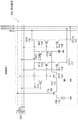
また、図1は、実施例1に係るCMOSイメージセンサに用いられる、画素回路(読出し制御回路)の等価回路図を示すものである。
図1に示すように、本実施例における読出し制御回路は、第1の信号経路および第2の信号経路の2系統の信号経路を備えている。
Further, FIG. 1 shows an equivalent circuit diagram of a pixel circuit (reading control circuit) used in the CMOS image sensor according to the first embodiment.
As shown in FIG. 1, the read control circuit in this embodiment includes two signal paths, a first signal path and a second signal path.
図1に示すように、光電変換素子であるフォトダイオード(PD)111は転送トランジスタ(TX)112を経て第1の浮遊拡散容量(FD1)113に接続される。第1の浮遊拡散容量(FD1)113は、オーバーフローゲート(OFG)122を経て第2の浮遊拡散容量(FD2)123に接続される。 As shown in FIG. 1, the photodiode (PD) 111, which is a photoelectric conversion element, is connected to the first floating diffusion capacitance (FD1) 113 via the transfer transistor (TX) 112. The first floating diffusion capacitance (FD1) 113 is connected to the second floating diffusion capacitance (FD2) 123 via the overflow gate (OFG) 122.
第1の信号経路である、第1の浮遊拡散容量(FD1)113の画素出力回路は、リセットトランジスタ1(RT1)114、ソースフォロアトランジスタ1(SF1)115、選択トランジスタ1(SL1)116で構成され、画素出力1(OUT1)117は垂直信号線204Aに接続されている。
The pixel output circuit of the first stray diffusion capacitance (FD1) 113, which is the first signal path, is composed of a reset transistor 1 (RT1) 114, a source follower transistor 1 (SF1) 115, and a selection transistor 1 (SL1) 116. The pixel output 1 (OUT1) 117 is connected to the
一方、第2の信号経路である、第2の浮遊拡散容量(FD2)123の画素出力回路は、リセットトランジスタ2(RT2)124、ソースフォロアトランジスタ2(SF2)
125、選択トランジスタ2(SL2)126で構成され、画素出力2(OUT2)127は、上記とは別の垂直信号線204Bに接続されている。
On the other hand, the pixel output circuit of the second stray diffusion capacitance (FD2) 123, which is the second signal path, includes the reset transistor 2 (RT2) 124 and the source follower transistor 2 (SF2).
It is composed of 125 and the selection transistor 2 (SL2) 126, and the pixel output 2 (OUT2) 127 is connected to a
リセットトランジスタ1(RT1)114、ソースフォロアトランジスタ1(SF1)115、リセットトランジスタ2(RT2)124、ソースフォロアトランジスタ2(SF2)125の各ドレイン電極は、画素電源(VDD)118に接続されている。 The drain electrodes of the reset transistor 1 (RT1) 114, the source follower transistor 1 (SF1) 115, the reset transistor 2 (RT2) 124, and the source follower transistor 2 (SF2) 125 are connected to the pixel power supply (VDD) 118. ..
また、転送トランジスタ(TX)112、オーバーフローゲート(OFG)122、リセットトランジスタ1(RT1)114、リセットトランジスタ2(RT2)124、選択トランジスタ1(SL1)116、選択トランジスタ2(SL2)126の各ゲート電極は、それぞれの画素駆動配線203に接続されている。
Further, each gate of the transfer transistor (TX) 112, the overflow gate (OFG) 122, the reset transistor 1 (RT1) 114, the reset transistor 2 (RT2) 124, the selection transistor 1 (SL1) 116, and the selection transistor 2 (SL2) 126. The electrodes are connected to the respective
図1に示す単位画素202の画素回路(読出し制御回路)において、フォトダイオード(PD)111は、入射光の強度に応じた量の負電荷を蓄積する。このフォトダイオード(PD)111のアノードは接地され、カソードは転送トランジスタ(TX)112、および第1の浮遊拡散容量(FD1)113を介してソースフォロアトランジスタ1(SF1)115のゲートに接続される。転送トランジスタ(TX)112のゲートは、垂直操作回路209からの画素駆動配線203(TX)に接続され、転送信号が入力される。 In the pixel circuit (reading control circuit) of the unit pixel 202 shown in FIG. 1, the photodiode (PD) 111 accumulates a negative charge in an amount corresponding to the intensity of the incident light. The anode of the photodiode (PD) 111 is grounded, and the cathode is connected to the gate of the source follower transistor 1 (SF1) 115 via the transfer transistor (TX) 112 and the first stray diffusion capacitance (FD1) 113. .. The gate of the transfer transistor (TX) 112 is connected to the pixel drive wiring 203 (TX) from the vertical operation circuit 209, and a transfer signal is input.
第1の信号経路において、ソースフォロアトランジスタ1(SF1)115および選択トランジスタ1(SL1)116は、画素電源(VDD)118と画素出力1(OUT1)117との間に直列接続される。選択トランジスタ1(SL1)116のゲートは、垂直操作回路209からの画素駆動配線203(SL1)に接続され、選択信号が入力される。リセットトランジスタ1(RT1)114は、画素電源(VDD)118とソースフォロアトランジスタ1(SF1)115のゲートとの間に接続される。リセットトランジスタ1(RT1)114のゲートは、垂直操作回路209からの画素駆動配線203(RT1)に接続され、リセット信号を入力される。 In the first signal path, the source follower transistor 1 (SF1) 115 and the selection transistor 1 (SL1) 116 are connected in series between the pixel power supply (VDD) 118 and the pixel output 1 (OUT1) 117. The gate of the selection transistor 1 (SL1) 116 is connected to the pixel drive wiring 203 (SL1) from the vertical operation circuit 209, and the selection signal is input. The reset transistor 1 (RT1) 114 is connected between the pixel power supply (VDD) 118 and the gate of the source follower transistor 1 (SF1) 115. The gate of the reset transistor 1 (RT1) 114 is connected to the pixel drive wiring 203 (RT1) from the vertical operation circuit 209, and a reset signal is input.
また、第1の浮遊拡散容量(FD1)113は、ソースフォロアトランジスタ1(SF1)115のゲートに接続される。
前述したように、第2の浮遊拡散容量(FD2)123は、オーバーフローゲート(OFG)122を経て第1の浮遊拡散容量(FD1)113に接続されており、第1の浮遊拡散容量(FD1)113に蓄積された電荷が、オーバーフローゲート(OFG)122から溢れると、第2の浮遊拡散容量(FD2)123に入力される。
Further, the first stray diffusion capacitance (FD1) 113 is connected to the gate of the source follower transistor 1 (SF1) 115.
As described above, the second floating diffusion capacity (FD2) 123 is connected to the first floating diffusion capacity (FD1) 113 via the overflow gate (OFG) 122, and is connected to the first floating diffusion capacity (FD1) 113. When the electric charge accumulated in 113 overflows from the overflow gate (OFG) 122, it is input to the second floating diffusion capacitance (FD2) 123.
第2の信号経路において、ソースフォロアトランジスタ2(SF2)125および選択トランジスタ2(SL2)126は、画素電源(VDD)118と画素出力2(OUT2)127との間に直列接続される。選択トランジスタ2(SL2)126のゲートは、垂直操作回路209からの画素駆動配線203(SL2)に接続され、選択信号が入力される。リセットトランジスタ2(RT2)124は、画素電源(VDD)118とソースフォロアトランジスタ2(SF2)125のゲートとの間に接続される。リセットトランジスタ2(RT2)124のゲートは、垂直操作回路209からの画素駆動配線203(RT2)に接続され、リセット信号を入力される。 In the second signal path, the source follower transistor 2 (SF2) 125 and the selection transistor 2 (SL2) 126 are connected in series between the pixel power supply (VDD) 118 and the pixel output 2 (OUT2) 127. The gate of the selection transistor 2 (SL2) 126 is connected to the pixel drive wiring 203 (SL2) from the vertical operation circuit 209, and the selection signal is input. The reset transistor 2 (RT2) 124 is connected between the pixel power supply (VDD) 118 and the gate of the source follower transistor 2 (SF2) 125. The gate of the reset transistor 2 (RT2) 124 is connected to the pixel drive wiring 203 (RT2) from the vertical operation circuit 209, and a reset signal is input.
また、第2の浮遊拡散容量(FD2)123は、ソースフォロアトランジスタ2(SF2)125のゲートに接続される。
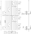
図3は、図1に示す画素回路(読出し制御回路)202を用いて、信号読出しを行った場合における、各トランジスタの入力信号を表すタイムチャートである。
Further, the second floating diffusion capacitance (FD2) 123 is connected to the gate of the source follower transistor 2 (SF2) 125.
FIG. 3 is a time chart showing an input signal of each transistor when a signal is read out using the pixel circuit (reading control circuit) 202 shown in FIG.
図3において、各チャートは、選択トランジスタ1、2(SL1、2)116、126
、リセットトランジスタ1、2(RT1、2)114、124、第1の転送トランジスタ(TX)112、オーバーフローゲート(OFG)122の信号波形を示すものであり、SL、RT、TXおよびOFGの後段に記されたかっこの中の数字((1)から(n))は、対応ライン(行)上の1行目からn行目の単位画素であることを示している。
In FIG. 3, each chart shows the
The signal waveforms of the
図3に示されるように、選択トランジスタ1、2(SL1、2)116、126がオン状態(SL1とSL2が「H」レベル)の時にリセットトランジスタ1、2(RT1、2)114、124をオン状態(RT1とRT2が「H」レベル)とすることで、第1、第2の浮遊拡散容量(FD1、2)113、123がリセットされる。このことは、全ての行について同じである。
転送トランジスタ(TX)112をオン状態(TX(1)が「H」レベル)とすることで、フォトダイオード(PD)111の信号電荷が転送トランジスタ(TX)112を経て第1の浮遊拡散容量(FD1)113へ移動し、第1の浮遊拡散容量(FD1)113で信号電圧へ変換される。第1の浮遊拡散容量(FD1)113の飽和容量を超える信号電荷が流入してきた場合には、オーバーフローゲート(OFG)122を経て第2の浮遊拡散容量(FD2)123へ移動し、この第2の浮遊拡散容量(FD2)123で信号電圧へ変換される。
As shown in FIG. 3, when the
By setting the transfer transistor (TX) 112 to the ON state (TX (1) is at the “H” level), the signal charge of the photodiode (PD) 111 passes through the transfer transistor (TX) 112 and the first stray diffusion capacitance ( It moves to FD1) 113 and is converted into a signal voltage by the first stray diffusion capacitance (FD1) 113. When a signal charge exceeding the saturation capacity of the first floating diffusion capacitance (FD1) 113 flows in, it moves to the second floating diffusion capacitance (FD2) 123 via the overflow gate (OFG) 122, and this second floating diffusion capacitance (FD2) 123. It is converted into a signal voltage by the stray diffusion capacitance (FD2) 123 of.
ここで、第1の浮遊拡散容量(FD1)113の容量を小さくして変換ゲインを高く設定し、第2の浮遊拡散容量(FD2)123の容量を大きくして変換ゲインを低く設定する。
オーバーフローゲート(OFG)122のゲート電圧(閾値)は第1の浮遊拡散容量(FD1)113の飽和容量を所定の値に設定するため、電圧値を調整した上で所定の一定値に固定される。第1の浮遊拡散容量(FD1)113と第2の浮遊拡散容量(FD2)123の信号電圧はソースフォロアトランジスタ1(SF1)115とソースフォロアトランジスタ2(SF2)125のゲート電極へそれぞれ印加され、ソースフォロアトランジスタ1(SF1)115とソースフォロアトランジスタ2(SF2)125からの出力電流が、画素出力1(OUT1)と画素出力2(OUT2)から別々の垂直信号線204A、Bに出力される。
Here, the capacitance of the first floating diffusion capacitance (FD1) 113 is reduced to set the conversion gain high, and the capacitance of the second floating diffusion capacitance (FD2) 123 is increased to set the conversion gain low.
The gate voltage (threshold value) of the overflow gate (OFG) 122 is fixed to a predetermined constant value after adjusting the voltage value in order to set the saturation capacity of the first stray diffusion capacitance (FD1) 113 to a predetermined value. .. The signal voltages of the first stray diffusion capacitance (FD1) 113 and the second stray diffusion capacitance (FD2) 123 are applied to the gate electrodes of the source follower transistor 1 (SF1) 115 and the source follower transistor 2 (SF2) 125, respectively. The output currents from the source follower transistor 1 (SF1) 115 and the source follower transistor 2 (SF2) 125 are output from the pixel output 1 (OUT1) and the pixel output 2 (OUT2) to separate
図4は、実施例1に係る単位画素の平面模式図の一例を示すものであり、図1の単位画素の等価回路図に対応させたものである。
すなわち、この平面模式図では、フォトダイオード(PD)111は、転送トランジスタ(TX)112、第1の浮遊拡散容量(FD1)113、リセットトランジスタ1(RT1)114および画素電源(VDD)118を介してソースフォロアトランジスタ1(SF1)115のゲートに接続される、ことが示されている。ソースフォロアトランジスタ1(SF1)115は、選択トランジスタ1(SL1)116を介して画素出力1(OUT1)117に接続される。
FIG. 4 shows an example of a schematic plan view of the unit pixel according to the first embodiment, and corresponds to the equivalent circuit diagram of the unit pixel of FIG.
That is, in this schematic plan view, the photodiode (PD) 111 is via the transfer transistor (TX) 112, the first stray diffusion capacitance (FD1) 113, the reset transistor 1 (RT1) 114, and the pixel power supply (VDD) 118. It is shown that it is connected to the gate of the source follower transistor 1 (SF1) 115. The source follower transistor 1 (SF1) 115 is connected to the pixel output 1 (OUT1) 117 via the selection transistor 1 (SL1) 116.
一方、この平面模式図では、フォトダイオード(PD)111は、転送トランジスタ(TX)112、オーバーフローゲート(OFG)122、第2の浮遊拡散容量(FD2)123、リセットトランジスタ2(RT2)124、画素電源(VDD)118を介してソースフォロアトランジスタ2(SF2)125のゲートに接続される、ことが示されている。ソースフォロアトランジスタ2(SF2)125は、選択トランジスタ2(SL2)126を介して画素出力2(OUT2)127に接続される。 On the other hand, in this schematic plan view, the photodiode (PD) 111 includes a transfer transistor (TX) 112, an overflow gate (OFG) 122, a second stray diffusion capacitance (FD2) 123, a reset transistor 2 (RT2) 124, and a pixel. It has been shown to be connected to the gate of the source follower transistor 2 (SF2) 125 via the power supply (VDD) 118. The source follower transistor 2 (SF2) 125 is connected to the pixel output 2 (OUT2) 127 via the selection transistor 2 (SL2) 126.
図5は、低照度である場合について、図4における平面模式図のA−A’線断面を示すものであり、(A)は露光時について、(B)は信号電荷の移動時について、各々示すものである。
なお、各ポテンシャルが示されている部位の名称は、その部位の上方に記号にて示され
ている(図6において同じ)。
また、図中でクロスハッチングで示す部分は、元から、第1の浮遊拡散容量(FD1)113および第2の浮遊拡散容量(FD2)123に存在する電子量を示すものであり、梨地で示す部分は、フォトダイオード(PD)111中、またはフォトダイオード(PD)111から流入した光電子量を示すものである(図6において同じ)。
これらの図から明らかなように、低照度である場合には、フォトダイオード(PD)111の光電子の量が少ないため、転送トランジスタ(TX)112がオン状態のときには、光電子は第1の浮遊拡散容量(FD1)113に移動するだけで、第2の浮遊拡散容量(FD2)123には移動しない。このため第2の浮遊拡散容量(FD2)123は元の電圧VDDのままである。
5A and 5B show a cross section taken along the line AA'in the schematic plan view of FIG. 4 in the case of low illuminance, in which FIG. 5A is for exposure and FIG. 5B is for signal charge transfer. It shows.
The name of the part where each potential is shown is indicated by a symbol above the part (same in FIG. 6).
Further, the portion indicated by cross-hatching in the figure indicates the amount of electrons existing in the first floating diffusion capacitance (FD1) 113 and the second floating diffusion capacitance (FD2) 123 from the beginning, and is shown in satin finish. The portion indicates the amount of photoelectrons flowing into the photodiode (PD) 111 or from the photodiode (PD) 111 (same in FIG. 6).
As is clear from these figures, the amount of photoelectrons in the photodiode (PD) 111 is small when the illuminance is low, so that when the transfer transistor (TX) 112 is in the ON state, the photoelectrons are first suspended and diffused. It only moves to the capacitance (FD1) 113, not to the second floating diffusion capacitance (FD2) 123. Therefore, the second stray diffusion capacitance (FD2) 123 remains the original voltage VDD.
一方、図6は、高照度である場合について、図4における平面模式図のA−A’線断面を示すものであり、(A)は露光時について、(B)は信号電荷の移動時について、各々示すものである。
これらの図から明らかなように、高照度である場合には、フォトダイオード(PD)111の光電子の量が多いため、転送トランジスタ(TX)112がオン状態のときには、光電子は第1の浮遊拡散容量(FD1)113に移動するのと同時に、この第1の浮遊拡散容量(FD1)113から溢れ、第2の浮遊拡散容量(FD2)123にも移動する。このため第2の浮遊拡散容量(FD2)123では元の電圧VDDから光電子量が増大した状態となる。
On the other hand, FIG. 6 shows a cross section taken along the line AA'in the schematic plan view of FIG. 4 in the case of high illuminance, (A) is for exposure, and (B) is for movement of signal charge. , Each is shown.
As is clear from these figures, the amount of photoelectrons in the photodiode (PD) 111 is large when the illuminance is high, so that when the transfer transistor (TX) 112 is in the ON state, the photoelectrons are first suspended and diffused. At the same time as moving to the capacity (FD1) 113, it overflows from the first floating diffusion capacity (FD1) 113 and moves to the second floating diffusion capacity (FD2) 123. Therefore, in the second floating diffusion capacitance (FD2) 123, the amount of photoelectrons is increased from the original voltage VDD.
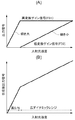
図7(A)は、第1の浮遊拡散容量FD1(113)を経て画素出力回路から出力される高変換ゲインの信号と、第2の浮遊拡散容量FD2(123)を経て画素出力回路から出力される低変換ゲインの信号の入射光強度に対する関係を示す図である。
また、図7(B)は、高変換ゲイン(FD1)の信号と低変換ゲイン(FD2)の信号を、この固体撮像素子の外部における後段の信号処理部(図示されていない)において信号合成される信号(合成後出力信号)を入射光強度との関係において示す図である。
この図7(A)からも分かるように、高変換ゲイン(FD1)の信号は、一定の出力値で飽和し(飽和点)、この入射光強度のときに、丁度、低変換ゲイン(FD2)の信号が立ち上がるので、この低変換ゲイン(FD2)の信号の立ち上がり点で、両信号を繋ぎ合わせるように合成すればよい。
図示するように、この合成後の信号は、低照度時には傾きが大となって、高S/Nとされ、一方、高照度時には傾きが小となって、広ダイナミックレンジとされる。したがって、1つの信号によって、相反する2つの特性を発揮させることができる。したがって、低輝度の被写体に合わせることで高輝度の被写体の信号が飽和してしまったり、高輝度の被写体に合わせることで低輝度の被写体の信号が雑音に埋もれてしまったり、というような不都合を回避することができる。
さらに、本実施例では、光電変換部を分割しないで解像度特性を優れたものとすることができ、露光時間を分割しないで動画撮像特性を優れたものとすることができ、さらに高感度、高S/N化と広ダイナミックレンジ化のトレードオフを解消することができる。
FIG. 7A shows a high conversion gain signal output from the pixel output circuit via the first stray diffusion capacitance FD1 (113) and an output from the pixel output circuit via the second stray diffusion capacitance FD2 (123). It is a figure which shows the relationship with respect to the incident light intensity of the signal of the low conversion gain to be made.
Further, in FIG. 7B, a signal having a high conversion gain (FD1) and a signal having a low conversion gain (FD2) are signal-synthesized in a signal processing unit (not shown) in a subsequent stage outside the solid-state image sensor. It is a figure which shows the signal (output signal after synthesis) in relation to the incident light intensity.
As can be seen from FIG. 7A, the high conversion gain (FD1) signal is saturated at a constant output value (saturation point), and at this incident light intensity, the low conversion gain (FD2) is just right. Since the signal of (FD2) rises, both signals may be combined so as to be connected at the rising point of the signal of this low conversion gain (FD2).
As shown in the figure, the combined signal has a large slope at low illuminance and a high S / N, while it has a small slope at high illuminance and has a wide dynamic range. Therefore, one signal can exert two contradictory characteristics. Therefore, matching with a low-brightness subject may saturate the signal of a high-brightness subject, or matching with a high-brightness subject may cause the signal of a low-brightness subject to be buried in noise. It can be avoided.
Further, in this embodiment, the resolution characteristics can be improved without dividing the photoelectric conversion unit, the moving image imaging characteristics can be improved without dividing the exposure time, and the sensitivity and high sensitivity can be further improved. The trade-off between S / N and wide dynamic range can be eliminated.
次に、図8は、単位画素のポテンシャルシミュレーションによる結果を表す平面図である。転送トランジスタ(TX)112のゲート電極には2.5V、オーバーフローゲート(OFG)122のゲート電極には1.9V、リセットトランジスタ1(RT1)114、リセットトランジスタ2(RT2)124、ソースフォロアトランジスタ1(SF1)115、ソースフォロアトランジスタ2(SF2)125、選択トランジスタ1(SL1)116、選択トランジスタ2(SL2)126のゲート電極には0Vが印加されている。
なお、図8中において、文字を挿入することによる煩雑さによって、各部を表す線等が見難くなることを避けるため、図8の各部の番号は省略している。
Next, FIG. 8 is a plan view showing the result of the potential simulation of the unit pixel. 2.5V for the gate electrode of the transfer transistor (TX) 112, 1.9V for the gate electrode of the overflow gate (OFG) 122, reset transistor 1 (RT1) 114, reset transistor 2 (RT2) 124,
In FIG. 8, the numbers of the respective parts in FIG. 8 are omitted in order to prevent the lines and the like representing the respective parts from becoming difficult to see due to the complexity caused by inserting the characters.
また、図9は、図8におけるB-B’線断面図である。図9の例では、フォトダイオー
ド(PD)111に光電子が空の状態を示している。
すなわち、このB-B’線断面において、フォトダイオード(PD)111は、伝導帯
の底に電子がたまっていない状態となっており、空の状態となっていることが示されている。一方、第1の浮遊拡散容量(FD1)113および転送トランジスタ(TX)112下部には、電子が所定量入っている状態が示されている。
Further, FIG. 9 is a cross-sectional view taken along the line BB'in FIG. In the example of FIG. 9, a state in which photoelectrons are empty in the photodiode (PD) 111 is shown.
That is, in this BB'line cross section, it is shown that the photodiode (PD) 111 is in a state where electrons are not accumulated at the bottom of the conduction band and is in an empty state. On the other hand, a state in which a predetermined amount of electrons are contained in the first floating diffusion capacitance (FD1) 113 and the lower portion of the transfer transistor (TX) 112 is shown.
一方、図10は、図8におけるC-C’線断面図である。図10の例では、第1の浮遊
拡散容量(FD1)113において、電子が飽和した状態が示されている。
すなわち、第1の浮遊拡散容量(FD1)113は光電子が飽和状態(オーバーフローゲート(OFG)122が満杯状態)となっており、これ以上第1の浮遊拡散容量(FD1)113に光電子が入ってくると、この光電子は第2の浮遊拡散容量(FD2)123に流入する。なお、図10に示す状態では、第2の浮遊拡散容量(FD2)123はVDD=3.3Vの状態であって元の電子の状態であり、第1の浮遊拡散容量(FD1)113からの光電子はまだ流入していない状態とされている。
<実施例2>
On the other hand, FIG. 10 is a cross-sectional view taken along the line CC'in FIG. In the example of FIG. 10, a state in which electrons are saturated is shown in the first floating diffusion capacitance (FD1) 113.
That is, the first floating diffusion capacitance (FD1) 113 is saturated with photoelectrons (the overflow gate (OFG) 122 is full), and the first floating diffusion capacitance (FD1) 113 is further filled with photoelectrons. When it comes, the photoelectrons flow into the second floating diffusion capacitance (FD2) 123. In the state shown in FIG. 10, the second floating diffusion capacitance (FD2) 123 is in the state of VDD = 3.3V and is the original state of electrons, and is from the first floating diffusion capacitance (FD1) 113. It is said that photoelectrons have not yet flowed in.
<Example 2>
以下、本発明の実施例2について、上記図面を参照しながら説明する。
なお、実施例2のものは実施例1のものと共通する部分も多いので、以下の説明において、実施例1の各部に付した番号に200を加えた番号を実施例1の各部に対応した実施例2の各部に付し、その詳しい説明は省略する場合がある。
図12は、実施例2に係る単位画素の画素アレイを有する固体撮像素子、具体的にはCMOSイメージセンサのシステム構成を示すものであって、実施例1について示す図2と
対応するものである。CMOSイメージセンサ400は、光電変換素子を含む単位画素402がアレイ状に2次元配列され、画素駆動配線403、垂直信号線404と接続している画素アレイ401を有するとともに、周辺回路として、カラム信号処理回路405、センサ外部のデジタルCDS回路410と接続される出力回路406、制御回路407、水平走査回路408、および垂直走査回路409から構成されている。
ここで、カラム信号処理回路405および水平走査回路408が、図中の上方および下方に配されているのは、片側に配された場合に比べ、フレーム周波数を2倍にすることができるという理由からである。
Hereinafter, Example 2 of the present invention will be described with reference to the above drawings.
In addition, since the thing of Example 2 has many parts in common with the thing of Example 1, in the following description, the number given to each part of Example 1 plus 200 corresponds to each part of Example 1. It is attached to each part of the second embodiment, and the detailed description thereof may be omitted.
FIG. 12 shows a system configuration of a solid-state image sensor having a pixel array of unit pixels according to the second embodiment, specifically, a CMOS image sensor, and corresponds to FIG. 2 shown in the first embodiment. .. The CMOS image sensor 400 has a pixel array 401 in which unit pixels 402 including a photoelectric conversion element are two-dimensionally arranged in an array and connected to a pixel drive wiring 403 and a vertical signal line 404, and a column signal as a peripheral circuit. It is composed of a processing circuit 405, an
Here, the reason why the column signal processing circuit 405 and the horizontal scanning circuit 408 are arranged above and below in the figure is that the frame frequency can be doubled as compared with the case where they are arranged on one side. Because.
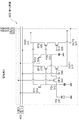
また、図11は、実施例2に係るCMOSイメージセンサに用いられる、画素回路(読出し制御回路)の等価回路図を示すものである。本等価回路は、光電変換部から信号電荷を読み出す画素回路が、前記第1の浮遊拡散容量手段につき、転送トランジスタは配置されていないのでトランジスタ3個から、および前記第2の浮遊拡散容量手段につきオーバーフローゲートを含めてトランジスタ4個から構成され、低照度状態では高S/N状態、高照度状態では広ダイナミックレンジ状態となる信号を生成する構成とされている。
図11に示すように、実施例2における読出し制御回路は、第1の信号経路および第2の信号経路の2系統の信号経路を備えている。
Further, FIG. 11 shows an equivalent circuit diagram of a pixel circuit (reading control circuit) used in the CMOS image sensor according to the second embodiment. In this equivalent circuit, the pixel circuit that reads the signal charge from the photoelectric conversion unit is the first floating diffusion capacitance means, and since no transfer transistor is arranged, the pixel circuit is from three transistors, and the second floating diffusion capacitance means. It is composed of four transistors including an overflow gate, and is configured to generate a signal that is in a high S / N state in a low illuminance state and in a wide dynamic range state in a high illuminance state.
As shown in FIG. 11, the read control circuit according to the second embodiment includes two signal paths, a first signal path and a second signal path.
図11に示すように、光電変換素子であるフォトダイオード(PD)311は第1の浮遊拡散容量(FD1)313に接続される。第1の浮遊拡散容量(FD1)313は、オーバーフローゲート(OFG)322を経て第2の浮遊拡散容量(FD2)323に接続される。 As shown in FIG. 11, the photodiode (PD) 311 which is a photoelectric conversion element is connected to the first floating diffusion capacitance (FD1) 313. The first floating diffusion capacitance (FD1) 313 is connected to the second floating diffusion capacitance (FD2) 323 via an overflow gate (OFG) 322.
第1の信号経路である、第1の浮遊拡散容量(FD1)313の画素出力回路は、リセットトランジスタ1(RT1)314、ソースフォロアトランジスタ1(SF1)315、選択トランジスタ1(SL1)316で構成され、画素出力1(OUT1)317は垂
直信号線404Aに接続されている。
The pixel output circuit of the first stray diffusion capacitance (FD1) 313, which is the first signal path, is composed of a reset transistor 1 (RT1) 314, a source follower transistor 1 (SF1) 315, and a selection transistor 1 (SL1) 316. The pixel output 1 (OUT1) 317 is connected to the
一方、第2の信号経路である、第2の浮遊拡散容量(FD2)323の画素出力回路は、リセットトランジスタ2(RT2)324、ソースフォロアトランジスタ2(SF2)325、選択トランジスタ2(SL2)326で構成され、画素出力2(OUT2)327は、上記とは別の垂直信号線404Bに接続されている。
On the other hand, the pixel output circuit of the second stray diffusion capacitance (FD2) 323, which is the second signal path, includes the reset transistor 2 (RT2) 324, the source follower transistor 2 (SF2) 325, and the selection transistor 2 (SL2) 326. The pixel output 2 (OUT2) 327 is connected to a
リセットトランジスタ1(RT1)314、ソースフォロアトランジスタ1(SF1)315、リセットトランジスタ2(RT2)324、ソースフォロアトランジスタ2(SF2)325の各ドレイン電極は、画素電源(VDD)318に接続されている。 Each drain electrode of the reset transistor 1 (RT1) 314, the source follower transistor 1 (SF1) 315, the reset transistor 2 (RT2) 324, and the source follower transistor 2 (SF2) 325 is connected to the pixel power supply (VDD) 318. ..
また、オーバーフローゲート(OFG)322、リセットトランジスタ1(RT1)314、リセットトランジスタ2(RT2)324、選択トランジスタ1(SL1)316、選択トランジスタ2(SL2)326の各ゲート電極は、それぞれの画素駆動配線403に接続されている。 Further, each gate electrode of the overflow gate (OFG) 322, the reset transistor 1 (RT1) 314, the reset transistor 2 (RT2) 324, the selection transistor 1 (SL1) 316, and the selection transistor 2 (SL2) 326 is pixel-driven. It is connected to the wiring 403.
図11に示す単位画素402の画素回路(読出し制御回路)において、フォトダイオード(PD)311は、入射光の強度に応じた量の負電荷を発生する。このフォトダイオード(PD)311のアノードは接地され、カソードは第1の浮遊拡散容量(FD1)313を介してソースフォロアトランジスタ1(SF1)315のゲートに接続される。 In the pixel circuit (reading control circuit) of the unit pixel 402 shown in FIG. 11, the photodiode (PD) 311 generates a negative charge in an amount corresponding to the intensity of the incident light. The anode of the photodiode (PD) 311 is grounded and the cathode is connected to the gate of the source follower transistor 1 (SF1) 315 via a first stray diffusion capacitance (FD1) 313.
第1の信号経路において、ソースフォロアトランジスタ1(SF1)315および選択トランジスタ1(SL1)316は、画素電源(VDD)318と画素出力1(OUT1)317との間に直列接続される。選択トランジスタ1(SL1)316のゲートは、垂直操作回路409からの画素駆動配線403(SL1)に接続され、選択信号が入力される。リセットトランジスタ1(RT1)314は、画素電源(VDD)318とソースフォロアトランジスタ1(SF1)315のゲートとの間に接続される。リセットトランジスタ1(RT1)314のゲートは、垂直操作回路409からの画素駆動配線403(RT1)に接続され、リセット信号を入力される。 In the first signal path, the source follower transistor 1 (SF1) 315 and the selection transistor 1 (SL1) 316 are connected in series between the pixel power supply (VDD) 318 and the pixel output 1 (OUT1) 317. The gate of the selection transistor 1 (SL1) 316 is connected to the pixel drive wiring 403 (SL1) from the vertical operation circuit 409, and the selection signal is input. The reset transistor 1 (RT1) 314 is connected between the pixel power supply (VDD) 318 and the gate of the source follower transistor 1 (SF1) 315. The gate of the reset transistor 1 (RT1) 314 is connected to the pixel drive wiring 403 (RT1) from the vertical operation circuit 409, and a reset signal is input.
また、第1の浮遊拡散容量(FD1)313は、ソースフォロアトランジスタ1(SF1)315のゲートに接続される。
前述したように、第2の浮遊拡散容量(FD2)323は、オーバーフローゲート(OFG)322を経て第1の浮遊拡散容量(FD1)313に接続されており、第1の浮遊拡散容量(FD1)313に蓄積された電荷が、オーバーフローゲート(OFG)322から溢れると、第2の浮遊拡散容量(FD2)323に入力される。
Further, the first stray diffusion capacitance (FD1) 313 is connected to the gate of the source follower transistor 1 (SF1) 315.
As described above, the second floating diffusion capacity (FD2) 323 is connected to the first floating diffusion capacity (FD1) 313 via the overflow gate (OFG) 322, and the first floating diffusion capacity (FD1). When the electric charge accumulated in the 313 overflows from the overflow gate (OFG) 322, it is input to the second floating diffusion capacitance (FD2) 323.
第2の信号経路において、ソースフォロアトランジスタ2(SF2)325および選択トランジスタ2(SL2)326は、画素電源(VDD)318と画素出力2(OUT2)327との間に直列接続される。選択トランジスタ2(SL2)326のゲートは、垂直操作回路(図12においては番号409が付されている:以下同じ)からの画素駆動配線403(SL2)に接続され、選択信号が入力される。リセットトランジスタ2(RT2)324は、画素電源(VDD)318とソースフォロアトランジスタ2(SF2)325のゲートとの間に接続される。リセットトランジスタ2(RT2)324のゲートは、垂直操作回路409からの画素駆動配線403(RT2)に接続され、リセット信号を入力される。 In the second signal path, the source follower transistor 2 (SF2) 325 and the selection transistor 2 (SL2) 326 are connected in series between the pixel power supply (whether) 318 and the pixel output 2 (OUT2) 327. The gate of the selection transistor 2 (SL2) 326 is connected to the pixel drive wiring 403 (SL2) from the vertical operation circuit (numbered 409 in FIG. 12: the same applies hereinafter), and the selection signal is input. The reset transistor 2 (RT2) 324 is connected between the pixel power supply (VDD) 318 and the gate of the source follower transistor 2 (SF2) 325. The gate of the reset transistor 2 (RT2) 324 is connected to the pixel drive wiring 403 (RT2) from the vertical operation circuit 409, and a reset signal is input.
また、第2の浮遊拡散容量(FD2)323は、ソースフォロアトランジスタ2(SF2)325のゲートに接続される。
図13は、図11に示す画素回路(読出し制御回路)402を用いて、信号読出しを行
った場合における、各トランジスタの入力信号を表すタイムチャートである。
Further, the second floating diffusion capacitance (FD2) 323 is connected to the gate of the source follower transistor 2 (SF2) 325.
FIG. 13 is a time chart showing an input signal of each transistor when a signal is read out using the pixel circuit (reading control circuit) 402 shown in FIG.
図13において、各チャートは、選択トランジスタ1、2(SL1、2)316、326、リセットトランジスタ1、2(RT1、2)314、324、オーバーフローゲート(OFG)322の信号波形を示すものであり、SL、RTおよびOFGの後段に記されたかっこの中の数字((1)から(n))は、対応ライン(行)上の1行目からn行目の単位画素であることを示している。ADCは、AD変換器のサンプリングのタイミングを示している。従来技術では、画素回路がトランジスタ3個から構成される場合、駆動波形は後リセット方式のデジタル式相関二重サンプリング(デジタルCDS)によってリセットノイズを除去する。本方式は画素回路がトランジスタ3個から構成される場合からの改良であるので、駆動波形は後リセット方式のデジタルCDSによってリセットノイズを除去するようになっている。
In FIG. 13, each chart shows the signal waveforms of the
図13に示されるように、選択トランジスタ1、2(SL1、2)316、326がオン状態(SL1とSL2が「H」レベル)の時にリセットトランジスタ1、2(RT1、2)314、324をオン状態(RT1とRT2が「H」レベル)とすることで、第1、第2の浮遊拡散容量(FD1、2)313、323がリセットされる。このことは、全ての行について同じである。
フォトダイオード(PD)311の信号電荷は、第1の浮遊拡散容量(FD1)313へ移動し、第1の浮遊拡散容量(FD1)313で信号電圧へ変換される。第1の浮遊拡散容量(FD1)113の飽和容量を超える信号電荷が流入してきた場合には、オーバーフローゲート(OFG)322を経て第2の浮遊拡散容量(FD2)323へ移動し、この第2の浮遊拡散容量(FD2)323で信号電圧へ変換される。
As shown in FIG. 13, when the
The signal charge of the photodiode (PD) 311 moves to the first stray diffusion capacitance (FD1) 313 and is converted into a signal voltage by the first stray diffusion capacitance (FD1) 313. When a signal charge exceeding the saturation capacity of the first floating diffusion capacitance (FD1) 113 flows in, it moves to the second floating diffusion capacitance (FD2) 323 via the overflow gate (OFG) 322, and this second floating diffusion capacitance (FD2) It is converted into a signal voltage by the stray diffusion capacitance (FD2) 323 of.
ここで、第1の浮遊拡散容量(FD1)313の容量を小さくして変換ゲインを高く設定し、第2の浮遊拡散容量(FD2)323の容量を大きくして変換ゲインを低く設定する。
オーバーフローゲート(OFG)322のゲート電圧(閾値)は第1の浮遊拡散容量(FD1)313の飽和容量を所定の値に設定するため、電圧値を調整した上で所定の一定値に固定される。第1の浮遊拡散容量(FD1)313と第2の浮遊拡散容量(FD2)323の信号電圧はソースフォロアトランジスタ1(SF1)315とソースフォロアトランジスタ2(SF2)325のゲート電極へそれぞれ印加され、ソースフォロアトランジスタ1(SF1)315とソースフォロアトランジスタ2(SF2)325からの出力電流が、画素出力1(OUT1)と画素出力2(OUT2)から別々の垂直信号線404A、Bに出力される。
Here, the capacitance of the first floating diffusion capacitance (FD1) 313 is reduced to set the conversion gain high, and the capacitance of the second floating diffusion capacitance (FD2) 323 is increased to set the conversion gain low.
The gate voltage (threshold value) of the overflow gate (OFG) 322 is fixed to a predetermined constant value after adjusting the voltage value in order to set the saturation capacitance of the first stray diffusion capacitance (FD1) 313 to a predetermined value. .. The signal voltages of the first stray diffusion capacitance (FD1) 313 and the second stray diffusion capacitance (FD2) 323 are applied to the gate electrodes of the source follower transistor 1 (SF1) 315 and the source follower transistor 2 (SF2) 325, respectively. The output currents from the source follower transistor 1 (SF1) 315 and the source follower transistor 2 (SF2) 325 are output from the pixel output 1 (OUT1) and the pixel output 2 (OUT2) to separate
図14は、実施例2に係る単位画素の平面模式図の一例を示すものであり、図11の単位画素の等価回路図に対応させたものである。
すなわち、この平面模式図では、フォトダイオード(PD)311は、第1の浮遊拡散容量(FD1)313、リセットトランジスタ1(RT1)314および画素電源(VDD)318を介してソースフォロアトランジスタ1(SF1)315のゲートに接続される、ことが示されている。ソースフォロアトランジスタ1(SF1)315は、選択トランジスタ1(SL1)316を介して画素出力1(OUT1)317に接続される。
FIG. 14 shows an example of a schematic plan view of the unit pixel according to the second embodiment, and corresponds to the equivalent circuit diagram of the unit pixel of FIG.
That is, in this schematic plan view, the photodiode (PD) 311 is the source follower transistor 1 (SF1) via the first stray diffusion capacitance (FD1) 313, the reset transistor 1 (RT1) 314, and the pixel power supply (VDD) 318. ) It is shown to be connected to the gate of 315. The source follower transistor 1 (SF1) 315 is connected to the pixel output 1 (OUT1) 317 via the selection transistor 1 (SL1) 316.
一方、この平面模式図では、フォトダイオード(PD)311は、オーバーフローゲート(OFG)322、第2の浮遊拡散容量(FD2)323、リセットトランジスタ2(RT2)324、画素電源(VDD)318を介してソースフォロアトランジスタ2(SF2)325のゲートに接続される、ことが示されている。ソースフォロアトランジスタ2(SF2)325は、選択トランジスタ2(SL2)326を介して画素出力2(OUT2)327に接続される。 On the other hand, in this schematic plan view, the photodiode (PD) 311 is via an overflow gate (OFG) 322, a second stray diffusion capacitance (FD2) 323, a reset transistor 2 (RT2) 324, and a pixel power supply (VDD) 318. It is shown that it is connected to the gate of the source follower transistor 2 (SF2) 325. The source follower transistor 2 (SF2) 325 is connected to the pixel output 2 (OUT2) 327 via the selection transistor 2 (SL2) 326.
図15(A)は、低照度である場合について、平面模式図である図14のA−A’線断面を示すものであり、信号電荷の移動時について、示すものである。
なお、各ポテンシャルが示されている部位の名称は、その部位の上方に記号にて示されている。
また、図中でクロスハッチングで示す部分は、第1の浮遊拡散容量(FD1)313および第2の浮遊拡散容量(FD2)323に存在する電子量を示すものであり、梨地で示す部分は、フォトダイオード(PD)311から流入した光電子量を示すものである。
これらの図から明らかなように、低照度である場合には、フォトダイオード(PD)311の光電子の発生量が少ないため、光電子は第1の浮遊拡散容量(FD1)313に移動するだけで、第2の浮遊拡散容量(FD2)323には移動しない。このため第2の浮遊拡散容量(FD2)323は元の電圧VDDのままである。
FIG. 15A shows a cross section taken along the line AA'of FIG. 14 which is a schematic plan view in the case of low illuminance, and shows the time when the signal charge moves.
The name of the part where each potential is shown is indicated by a symbol above the part.
Further, the portion indicated by cross-hatching in the figure indicates the amount of electrons existing in the first floating diffusion capacitance (FD1) 313 and the second floating diffusion capacitance (FD2) 323, and the portion indicated by satin finish is It shows the amount of photoelectrons flowing in from the photodiode (PD) 311.
As is clear from these figures, when the illuminance is low, the amount of photoelectrons generated by the photodiode (PD) 311 is small, so that the photoelectrons only move to the first floating diffusion capacitance (FD1) 313. It does not move to the second floating diffusion capacitance (FD2) 323. Therefore, the second stray diffusion capacitance (FD2) 323 remains at the original voltage VDD.
一方、図15(B)は、高照度である場合について、図14におけるポテンシャル図のA−A’線断面を示すものであり、信号電荷の移動時について、示すものである。
これらの図から明らかなように、高照度である場合には、フォトダイオード(PD)311の光電子の発生量が多いため、光電子は第1の浮遊拡散容量(FD1)313に移動するのと同時に、この第1の浮遊拡散容量(FD1)313から溢れ、第2の浮遊拡散容量(FD2)323にも移動する。このため第2の浮遊拡散容量(FD2)323では元の電圧VDDから光電子量が増大した状態となる。
On the other hand, FIG. 15B shows the AA'line cross section of the potential diagram in FIG. 14 in the case of high illuminance, and shows the time when the signal charge moves.
As is clear from these figures, when the illuminance is high, the amount of photoelectrons generated by the photodiode (PD) 311 is large, so that the photoelectrons move to the first floating diffusion capacitance (FD1) 313 at the same time. , It overflows from the first floating diffusion capacity (FD1) 313 and moves to the second floating diffusion capacity (FD2) 323. Therefore, in the second floating diffusion capacitance (FD2) 323, the amount of photoelectrons is increased from the original voltage VDD.
なお、本実施例において、第1の浮遊拡散容量FD1(313)を経て画素出力回路から出力される高変換ゲインの信号と、第2の浮遊拡散容量FD2(323)を経て画素出力回路から出力される低変換ゲインの信号の入射光強度に対する関係は、実施例1におい
て図7を用いて行った説明と同様であるので、ここではその説明を省略する。
In this embodiment, a high conversion gain signal output from the pixel output circuit via the first floating diffusion capacitance FD1 (313) and an output from the pixel output circuit via the second floating diffusion capacitance FD2 (323). Since the relationship of the low conversion gain signal to the incident light intensity is the same as that described with reference to FIG. 7 in Example 1, the description thereof will be omitted here.
次に、図16は、単位画素のポテンシャルシミュレーションによる結果を表す平面図である。オーバーフローゲート(OFG)322のゲート電極には1.9V、リセットトランジスタ1(RT1)314、リセットトランジスタ2(RT2)324、ソースフォロアトランジスタ1(SF1)315、ソースフォロアトランジスタ2(SF2)325、選択トランジスタ1(SL1)316、選択トランジスタ2(SL2)326のゲート電極には0Vが印加されている。
実施例1における同様の図である図8と比べると、フォトダイオード(PD)311と第1の浮遊拡散容量(FD1)313との間に転送トランジスタ(TX)112が設けられていない点が相違している(図17について同じ)。
Next, FIG. 16 is a plan view showing the result of the potential simulation of a unit pixel. 1.9V, reset transistor 1 (RT1) 314, reset transistor 2 (RT2) 324, source follower transistor 1 (SF1) 315, source follower transistor 2 (SF2) 325, selected for the gate electrode of the overflow gate (OFG) 322. 0V is applied to the gate electrodes of the transistor 1 (SL1) 316 and the selection transistor 2 (SL2) 326.
Compared with FIG. 8 which is a similar diagram in the first embodiment, the difference is that the transfer transistor (TX) 112 is not provided between the photodiode (PD) 311 and the first stray diffusion capacitance (FD1) 313. (Same for FIG. 17).
また、図17は、図16におけるB-B’線断面図である。図17の例では、フォトダ
イオード(PD)311に光電子が空の状態を示している。
すなわち、このB-B’線断面において、フォトダイオード(PD)311は、伝導帯
の底に電子がたまっていない状態となっており、空の状態となっていることが示されている。一方、第1の浮遊拡散容量(FD1)313下部には、電子が所定量入っている状態が示されている。
Further, FIG. 17 is a cross-sectional view taken along the line BB'in FIG. In the example of FIG. 17, a state in which photoelectrons are empty is shown in the photodiode (PD) 311.
That is, in this BB'line cross section, the photodiode (PD) 311 is in a state where electrons are not accumulated at the bottom of the conduction band, and it is shown that the photodiode (PD) 311 is in an empty state. On the other hand, a state in which a predetermined amount of electrons are contained is shown in the lower part of the first floating diffusion capacitance (FD1) 313.
一方、図16におけるC-C’線断面図である図18は、実施例1における図8のC-C’線断面図と同様であるので、図18の説明は省略する。
以上のように形成された実施例2においては、実施例1のものと共通した構成も多いが、互いに相違する部分も存在する。以下、この相違点を中心として列挙形式にて説明する。
On the other hand, FIG. 18, which is a cross-sectional view taken along the line CC'in FIG. 16, is the same as the cross-sectional view taken along the line CC'of FIG. 8 in the first embodiment, and thus the description of FIG. 18 will be omitted.
In the second embodiment formed as described above, there are many configurations common to those of the first embodiment, but there are also parts different from each other. Hereinafter, this difference will be mainly described in an enumerated format.
<実施例1と実施例2の相違点>
実施例1は4トランジスタの画素回路を前提に広ダイナミックレンジ機能を持たせたものとしているのに対し、実施例2は3トランジスタの画素回路を前提に広ダイナミックレンジ機能を持たせたものとしている。したがって、実施例1と実施例2は、前提が4トランジスタの画素回路と3トランジスタの画素回路という点において、互いに相違する(下記相違点1)。
また、実施例1は、4トランジスタの画素回路に広ダイナミックレンジ機能を持たせたものであり、実施例2は、3トランジスタの画素回路に広ダイナミックレンジ機能を持たせたものであることから、互いに異なる画素回路に広ダイナミックレンジ機能を持たせたことによる作用効果の違いにおいて相違する(下記相違点2)。
<Differences between Example 1 and Example 2>
In the first embodiment, a wide dynamic range function is provided on the premise of a 4-transistor pixel circuit, whereas in the second embodiment, a wide dynamic range function is provided on the premise of a 3-transistor pixel circuit. .. Therefore, Example 1 and Example 2 differ from each other in that the premise is a 4-transistor pixel circuit and a 3-transistor pixel circuit (
Further, in the first embodiment, the pixel circuit of four transistors is provided with a wide dynamic range function, and in the second embodiment, the pixel circuit of three transistors is provided with a wide dynamic range function. There is a difference in the difference in action and effect due to having a wide dynamic range function in different pixel circuits (
[1]相違点1
(1)等価回路およびレイアウト
実施例1のものでは、第1の浮遊拡散容量につき、転送トランジスタ(TX)、リセットトランジスタ1(RT1)、ソースフォロアトランジスタ1(SF1)、および選択トランジスタ1(SL1)の4つのトランジスタ(4トランジスタ方式)で構成されており、第2の浮遊拡散容量につき、オーバーフローゲート(OFG)、リセットトランジスタ2(RT2)、ソースフォロアトランジスタ2(SF2)、および選択トランジスタ2(SL2)の4つのトランジスタで構成されている。
これに対し、実施例2のものでは、転送トランジスタ(TX)が設けられておらず、第1の浮遊拡散容量につき、リセットトランジスタ1(RT1)、ソースフォロアトランジスタ1(SF1)、および選択トランジスタ1(SL1)の3つのトランジスタ(3トランジスタ方式)で構成されており、第2の浮遊拡散容量につき、オーバーフローゲート(OFG)、リセットトランジスタ2(RT2)、ソースフォロアトランジスタ2(SF2)、および選択トランジスタ2(SL2)の4つのトランジスタで構成されている。
ただし、上記実施例1において、転送トランジスタ(TX)をON状態に保持することで、実施例2のような3トランジスタ用の駆動手法を適用することができる。
(2)駆動波形について
4トランジスタ方式の実施例1においては、リセットしてから信号を読む、前リセット方式を採用しているので、アナログCDSを画素とAD変換器の間に配置して、リセットノイズを除去することができる。
これに対し、3トランジスタ方式の実施例2においては、信号を読んでからリセットする、後リセット方式を採用することになるので、アナログCDSを画素とAD変換器の間に配置しても、リセットノイズを除去することができない。リセットノイズと1フレーム後の信号(信号+リセットノイズ)との間に、リセットノイズに関する相関がある(リセットノイズが略同一レベル)ので、デジタルCDSを適用してリセットノイズを除去することができる。なお、デジタルCDS(図12のデジタルCDS410を参照)としてはセンサチップ外部にフレームメモリを配置することにより構成することができる。
(3)最高フレーム周波数について
3トランジスタ方式の実施例2において、デジタルCDSを採用している場合、リセットノイズと、1フレーム後の信号(信号+リセットノイズ)とをAD変換器で読み出し、両者の差を求め、リセットノイズを相殺して、1フレーム分の画像信号としている(図13を参照)ので、画素以外の回路構成が同じ場合には、3トランジスタ方式を採用した場合は、4トランジスタ方式を採用した場合に比べて、最高フレーム周波数が1/2となる
。
(4)ノイズについて
4トランジスタ方式のリセットノイズと信号(信号+リセットノイズ)間のリセットノイズの相関性は、3トランジスタ方式のリセットノイズと信号(信号+リセットノイズ)間のリセットノイズの相関性よりも強いので、4トランジスタ方式の方がCDSでのリセットノイズのキャンセル効果が大きい。
(5)飽和信号量について
4トランジスタ方式の飽和信号量は、フォトダイオード(PD)の飽和電子量で規定される。露光時にフォトダイオード(PD)からあふれた電子は、浮遊拡散容量(FD)に移動し、リセット時に画素電源(VDD)に放出される。各フレームの蓄積期間にフォトダイオード(PD)からあふれた電子は使用されない。
一方、3トランジスタ方式の飽和信号量は、浮遊拡散容量(FD)の飽和電子量で規定される。フォトダイオード(PD)がn-型で不純物濃度が低いのに対し、浮遊拡散容量
(FD)はn+型で不純物濃度が高いので、浮遊拡散容量(FD)は状態密度が高く、面
積が小さくても、フォトダイオード(PD)よりも飽和電子量が大きい。各フレームの蓄積期間に浮遊拡散容量(FD)からあふれた電子は使用されない。
(6)フォトダイオード(PD)の感度について
各画素にマイクロレンズを付設していない場合、フォトダイオード(PD)の感度はフォトダイオード(PD)の面積により規定される。これに対して、各画素にマイクロレンズを付設している場合、入射光が画素上に集光されるので、フォトダイオード(PD)の感度はフォトダイオード(PD)の面積よりもマイクロレンズの性能に大きく影響される。4トランジスタ方式であるか、3トランジスタ方式であるかにによって、フォトダイオード(PD)の感度が大きく影響を受けるものではない。
[1]
(1) Equivalent circuit and layout In the first embodiment, the transfer transistor (TX), the reset transistor 1 (RT1), the source follower transistor 1 (SF1), and the selection transistor 1 (SL1) are used for the first stray diffusion capacitance. It is composed of four transistors (4-transistor system) of ) Is composed of four transistors.
On the other hand, in the second embodiment, the transfer transistor (TX) is not provided, and the reset transistor 1 (RT1), the source follower transistor 1 (SF1), and the
However, in the first embodiment, by holding the transfer transistor (TX) in the ON state, the driving method for three transistors as in the second embodiment can be applied.
(2) Drive waveform In Example 1 of the 4-transistor method, a pre-reset method is adopted in which the signal is read after resetting. Therefore, an analog CDS is placed between the pixel and the AD converter to reset. Noise can be removed.
On the other hand, in the second embodiment of the three-transistor method, a post-reset method is adopted in which the signal is read and then reset. Therefore, even if the analog CDS is placed between the pixel and the AD converter, the reset is performed. Noise cannot be removed. Since there is a correlation regarding reset noise between the reset noise and the signal after one frame (signal + reset noise) (the reset noise is at substantially the same level), the digital CDS can be applied to remove the reset noise. The digital CDS (see the
(3) Maximum frame frequency In Example 2 of the 3-transistor system, when digital CDS is adopted, the reset noise and the signal (signal + reset noise) after one frame are read out by the AD converter, and both are read. Since the difference is obtained and the reset noise is offset to obtain an image signal for one frame (see FIG. 13), if the circuit configuration other than the pixels is the same, the 4-transistor method is used when the 3-transistor method is adopted. The maximum frame frequency is halved as compared with the case of adopting.
(4) Noise The correlation between the 4-transistor reset noise and the reset noise between the signal (signal + reset noise) is based on the correlation between the 3-transistor reset noise and the signal (signal + reset noise). The 4-transistor method has a greater effect of canceling reset noise in CDS.
(5) Saturation signal amount The saturation signal amount of the 4-transistor system is defined by the saturated electron amount of the photodiode (PD). The electrons overflowing from the photodiode (PD) during exposure move to the stray diffusion capacitance (FD) and are emitted to the pixel power supply (VDD) at reset. The electrons overflowing from the photodiode (PD) during the storage period of each frame are not used.
On the other hand, the saturation signal amount of the three-transistor system is defined by the saturated electron amount of the stray diffusion capacitance (FD). Since the photodiode (PD) is n-type and the impurity concentration is low, the floating diffusion capacitance (FD) is n + type and the impurity concentration is high, so that the floating diffusion capacitance (FD) has a high density of states and a small area. However, the amount of saturated electrons is larger than that of the photodiode (PD). The electrons overflowing from the floating diffusion capacitance (FD) during the accumulation period of each frame are not used.
(6) Sensitivity of the photodiode (PD) When a microlens is not attached to each pixel, the sensitivity of the photodiode (PD) is defined by the area of the photodiode (PD). On the other hand, when a microlens is attached to each pixel, the incident light is focused on the pixel, so the sensitivity of the photodiode (PD) is higher than the area of the photodiode (PD). Is greatly influenced by. The sensitivity of the photodiode (PD) is not significantly affected by whether it is a 4-transistor system or a 3-transistor system.
[2]相違点2
(1)実施例1に係る4トランジスタ画素回路を前提に広ダイナミックレンジ機能を持たせたもの(以下、広DR機能付き4Tr.方式と称する場合がある)と、実施例2に係る3トランジスタ画素回路を前提に広ダイナミックレンジ機能を持たせたもの(以下、広DR機能付き3Tr.方式と称する場合がある)とを比較する前に、広DR機能を付加することによる効果について言及する。
この効果としては、(A)光電変換部を分割しないでも、解像度特性において優れていること、(B)露光時間を分割しないでも、動画撮像特性において優れていること、(C)画素出力信号において、高感度、高S/N化と、広ダイナミックレンジ化のトレードオ
フを解消し得ること、(D)超多画素において高フレーム周波数化ができること、が挙げられる。
(2)広DR機能の具体的な構成および効果
第1の浮遊拡散容量(FD1)と第2の浮遊拡散容量(FD2)がオーバーフローゲート(OFG)により接続して構成され、第1の浮遊拡散容量(FD1)の飽和電子量をオーバーフローゲート(OFG)のゲート電圧で調整するとともに、第1の浮遊拡散容量(FD1)からあふれた電子を第2の浮遊拡散容量(FD2)に移動させる。第1の浮遊拡散容量(FD1)と第2の浮遊拡散容量(FD2)は、各々の画素回路を介し、出力部OUT1、2から、互いに異なる信号を出力する。第1の浮遊拡散容量(FD1)の面積は小さく電荷電圧変換係数が高く、一方、第2の浮遊拡散容量(FD2)の面積は大きく電荷電圧変換係数が低い。低照度側は、第1の浮遊拡散容量(FD1)のみを使用して高感度、高S/N信号とし、一方、高照度側は、第1の浮遊拡散容量(FD1)および第2の
浮遊拡散容量(FD2)を使用して高感度、広DR信号とし、センサチップ外部で上記2つの信号を合成して、広DR信号を得る。
なお、広DR機能付き4Tr.方式と、広DR機能付き3Tr.方式の、各広DR機能自体は同じである。
(3)最高フレーム周波数について
画素出力が2種類、設けられていることから、それぞれに対してAD変換器を配設することで、最高フレーム周波数の低下を抑制して、従来技術と同等のフレーム周波数とすることが可能である。
(4)ノイズ、飽和信号量、およびフォトダイオード(PD)の感度について
ノイズ、飽和信号量、およびフォトダイオード(PD)の感度については、上記相違点1と同様である。
(5)広DR機能付き3Tr.方式に光電変換膜を用いる場合について
広DR機能付き3Tr.方式は、光電変換膜を積層することによって以下のような利点を有している(下記実施例3を参照)。この場合、光電変換膜の膜材料は特に限定されるものではない。
光電変換膜を積層した広DR機能付き3Tr.方式は、浮遊拡散容量(FD)のn+型
SiとVIAの金属が、バリアが無い状態で接続されているので、リセットの動作時間と信号の読出時間を短縮することができる(従来技術における3Tr.方式の場合と同等とすることができる)。
なお、光電変換膜を積層した広DR機能付き4Tr.方式は、構造として光電変換膜を積層することはできるが、フォトダイオード(PD)のn-型SiとVIAの金属が接続
され、浮遊拡散容量(FD)のn+型SiとVIAの金属の間に、フォトダイオード(P
D)のn-型Siが入り込み、バリアとして機能するので、リセットの動作時間と信号の
読出時間が長くなるため、問題がある。
また、実施例2に示すような、一般のフォトダイオード(PD)を用いた広DR機能付き3Tr.方式では、画素内においてトランジスタが7個存在し、これらトランジスタが占める面積割合が大きく、フォトダイオード(PD)の開口率が低くなってしまうため、マイクロレンズにより集光させることが必要であるが、後述する実施例3に示すような、光電変換膜を積層した広DR機能付き3Tr.方式のものでは、マイクロレンズなしに開口率を略100%にすることができる。
[2]
(1) A circuit having a wide dynamic range function on the premise of the 4-transistor pixel circuit according to the first embodiment (hereinafter, may be referred to as a 4Tr. Method with a wide DR function) and a three-transistor pixel according to the second embodiment. Before comparing with a circuit having a wide dynamic range function (hereinafter, may be referred to as a 3Tr. Method with a wide DR function), the effect of adding the wide DR function will be mentioned.
The effects are that (A) the photoelectric conversion unit is not divided and the resolution characteristics are excellent, (B) the exposure time is not divided and the moving image imaging characteristics are excellent, and (C) the pixel output signal. The trade-off between high sensitivity and high S / N and wide dynamic range can be eliminated, and (D) high frame frequency can be achieved with ultra-multi-pixels.
(2) Specific Configuration and Effect of Wide DR Function The first floating diffusion capacity (FD1) and the second floating diffusion capacity (FD2) are connected by an overflow gate (OFG), and the first floating diffusion capacity is configured. The saturated electron amount of the capacitance (FD1) is adjusted by the gate voltage of the overflow gate (OFG), and the electrons overflowing from the first floating diffusion capacitance (FD1) are moved to the second floating diffusion capacitance (FD2). The first floating diffusion capacitance (FD1) and the second floating diffusion capacitance (FD2) output signals different from each other from the output units OUT1 and OUT2 via their respective pixel circuits. The area of the first floating diffusion capacitance (FD1) is small and the charge-voltage conversion coefficient is high, while the area of the second floating diffusion capacitance (FD2) is large and the charge-voltage conversion coefficient is low. On the low-light side, only the first floating diffusion capacitance (FD1) is used to obtain a high-sensitivity, high S / N signal, while on the high-illuminance side, the first floating diffusion capacitance (FD1) and the second floating diffusion capacitance (FD1) are used. The diffusion capacitance (FD2) is used to obtain a high-sensitivity, wide DR signal, and the above two signals are combined outside the sensor chip to obtain a wide DR signal.
In addition, 4Tr. Method and 3Tr. With wide DR function. The wide DR function itself of the method is the same.
(3) Maximum frame frequency Since two types of pixel outputs are provided, by arranging an AD converter for each, a decrease in the maximum frame frequency can be suppressed and a frame equivalent to the conventional technology can be suppressed. It can be a frequency.
(4) Noise, Semaphore Signal Amount, and Photodiode (PD) Sensitivity The noise, saturation signal amount, and photodiode (PD) sensitivity are the same as in
(5) 3Tr. With wide DR function. When using a photoelectric conversion film as the method 3Tr. With wide DR function. The method has the following advantages by laminating the photoelectric conversion film (see Example 3 below). In this case, the film material of the photoelectric conversion film is not particularly limited.
3Tr. With wide DR function in which a photoelectric conversion film is laminated. In the method, since the n + type Si having a floating diffusion capacitance (FD) and the metal of VIA are connected without a barrier, the reset operation time and the signal reading time can be shortened (in the prior art). It can be the same as the case of the 3Tr. Method).
In addition, 4Tr. With a wide DR function in which a photoelectric conversion film is laminated. In the method, a photoelectric conversion film can be laminated as a structure, but the n-type Si of the photodiode (PD) and the metal of VIA are connected, and the n + type Si of the stray diffusion capacitance (FD) and the metal of VIA are connected. In between, the photodiode (P
Since the n-type Si of D) enters and functions as a barrier, there is a problem because the reset operation time and the signal reading time become long.
Further, as shown in Example 2, 3 Tr. With a wide DR function using a general photodiode (PD). In the method, there are seven transistors in the pixel, the area ratio occupied by these transistors is large, and the aperture ratio of the photodiode (PD) is low. Therefore, it is necessary to collect light with a microlens. As shown in Example 3 described later, a 3Tr. With a wide DR function in which a photoelectric conversion film is laminated. In the method, the aperture ratio can be set to about 100% without a microlens.
<実施例3>
上記実施例2において、フォトダイオード(PD)311を光電変換膜(PF)511に置き換えることができるので、このようにフォトダイオード(PD)311の部分のみを光電変換膜(PF)511に置き換えたものを実施例3として、以下に説明する。
<Example 3>
In the second embodiment, since the photodiode (PD) 311 can be replaced with the photoelectric conversion film (PF) 511, only the portion of the photodiode (PD) 311 is replaced with the photoelectric conversion film (PF) 511 in this way. This will be described below with reference to Example 3.
図19に示すように、実施例3に係る単位画素602の画素アレイを有する固体撮像素子、具体的にはCMOSイメージセンサに用いられる、画素回路(読出し制御回路)の等価回路図を示すものである。実施例3のものは、実施例2のものと共通する部分も多いので、以下の説明においては、実施例2の各部に付した番号に200を加えた番号を、実施例2の各部に対応した実施例3の各部に付し、その詳しい説明は省略する場合がある。 As shown in FIG. 19, it shows an equivalent circuit diagram of a pixel circuit (reading control circuit) used in a solid-state image sensor having a pixel array of unit pixels 602 according to the third embodiment, specifically, a CMOS image sensor. be. Since the thing of Example 3 has many parts in common with that of Example 2, in the following description, the number given to each part of Example 2 plus 200 corresponds to each part of Example 2. The detailed description of each part of the third embodiment may be omitted.
図19に示すように、実施例3における光電変換部は、光電変換膜(PF)511とされている。光電変換膜(PF)511は、各単位画素602上に積層されてなり、第1の浮遊拡散容量(FD1)513に接続される。
このように、光電変換膜を各単位画素602上に積層することにより、各単位画素602を配置するスペースを有効に利用することができ、画素の密度を高めることができる。
As shown in FIG. 19, the photoelectric conversion unit in Example 3 is a photoelectric conversion film (PF) 511. The photoelectric conversion film (PF) 511 is laminated on each unit pixel 602 and is connected to the first floating diffusion capacitance (FD1) 513.
By stacking the photoelectric conversion film on each unit pixel 602 in this way, the space for arranging each unit pixel 602 can be effectively used, and the density of the pixels can be increased.
図19に示す単位画素602の画素回路(読出し制御回路)において、光電変換膜(PF)511は、入射光の強度に応じた量の負電荷を発生する。この光電変換膜(PF)511の上部電極(UE)511Aは画素駆動配線(UE)603に接続され、下部電極(LE)511Bは第1の浮遊拡散容量(FD1)513を介してソースフォロアトランジスタ1(SF1)515のゲートに接続される。 In the pixel circuit (reading control circuit) of the unit pixel 602 shown in FIG. 19, the photoelectric conversion film (PF) 511 generates a negative charge in an amount corresponding to the intensity of the incident light. The upper electrode (UE) 511A of the photoelectric conversion film (PF) 511 is connected to the pixel drive wiring (UE) 603, and the lower electrode (LE) 511B is a source follower transistor via the first stray diffusion capacitance (FD1) 513. It is connected to the gate of 1 (SF1) 515.
図20は、図19に示す画素回路(読出し制御回路)を用いて、信号読出しを行った場合における、各トランジスタの入力信号を表すタイムチャートを示すものである。 FIG. 20 shows a time chart showing an input signal of each transistor when a signal is read out using the pixel circuit (reading control circuit) shown in FIG.
図20における各チャートは、実施例2において説明した図13における各チャート(最上部の上部電極(UE)のチャート以外)と同様であるので各チャートについての説明は省略する。
なお、上部電極(UE)には、常時、L信号が入力されることにより、光電変換膜がON状態であることが維持されるように構成されている。
Since each chart in FIG. 20 is the same as each chart in FIG. 13 (other than the chart of the uppermost upper electrode (UE)) described in the second embodiment, the description of each chart will be omitted.
The upper electrode (UE) is configured so that the photoelectric conversion film is maintained in the ON state by constantly inputting an L signal.
図21は、単位画素の平面模式図と断面模式図の一例を示すものであり、図19の単位画素602の等価回路図に対応させたものである。
すなわち、この平面模式図と断面模式図では、光電変換膜(PF)511は、上部電極(UE)511Aおよび下部電極(LE)511Bによって挟まれた構造とされており、図19に示すように、上部電極(UE)511Aは画素駆動配線(UE)603に接続され、下部電極(LE)511Bは第1の浮遊拡散容量(FD1)513に接続されている。実施例2の図14と比較すると、大きな面積を占めるフォトダイオード(PD)311が無いので、画素サイズの小型化を図ることができる。
FIG. 21 shows an example of a schematic plan view and a schematic cross-sectional view of a unit pixel, and corresponds to the equivalent circuit diagram of the unit pixel 602 of FIG.
That is, in the schematic plan view and the schematic cross-sectional view, the photoelectric conversion film (PF) 511 has a structure sandwiched between the upper electrode (UE) 511A and the lower electrode (LE) 511B, as shown in FIG. The upper electrode (UE) 511A is connected to the pixel drive wiring (UE) 603, and the lower electrode (LE) 511B is connected to the first stray diffusion capacitance (FD1) 513. Compared with FIG. 14 of the second embodiment, since there is no photodiode (PD) 311 that occupies a large area, the pixel size can be reduced.
また、この平面模式図と断面模式図では、下部電極(LE)511Bが第1の浮遊拡散容量(FD1)513に接続され、第1の浮遊拡散容量(FD1)513はオーバーフローゲート(OFG)522を経て第2の浮遊拡散容量(FD2)523に接続される、ことが示されている。 Further, in the schematic plan view and the schematic cross-sectional view, the lower electrode (LE) 511B is connected to the first floating diffusion capacitance (FD1) 513, and the first floating diffusion capacitance (FD1) 513 is an overflow gate (OFG) 522. It is shown that it is connected to the second floating diffusion capacitance (FD2) 523 via.
ここでは、光電変換膜(PF)511のキャリアは電子であり上部電極(UE)511Aに負電圧が印加されている場合について記載したが、キャリアが正孔であり上部電極(UE)に正電圧が印加されている場合についても同様の効果が得られる。 Here, the case where the carrier of the photoelectric conversion film (PF) 511 is an electron and a negative voltage is applied to the upper electrode (UE) 511A has been described, but the carrier is a hole and a positive voltage is applied to the upper electrode (UE). The same effect can be obtained when is applied.
本実施形態の撮像装置、駆動方法および読出し制御回路においては、上述したような構成とされたことで、低照度状態においては、飽和レベルを狭めることなく、線形かつ高S/Nの信号取得を行うことができ、高照度状態においては、線形領域での良好なS/Nを確保しつつダイナミックレンジを拡大することができる。
特に、低照度状態用と高照度状態用とで、それぞれが、画素出力回路と信号出力線を備えているため、同一時刻に同一光電変換部で得られた光信号を高フレーム周波数で読みだすことが可能であり、優れた動画撮像特性と解像度特性を有しつつ、超多画素を高フレーム周波数で読みだす撮像機器に対応することができる。
このような作用効果は、例えば、従来技術において説明した特許文献2(特許第5066704号公報)に記載のものに比べて、スーパーハイビジョン等のように、超多画素を高フレーム周波数で読みだす場合に、極めて有利である。
The image pickup apparatus, drive method, and readout control circuit of the present embodiment are configured as described above, so that linear and high S / N signal acquisition can be performed in a low illuminance state without narrowing the saturation level. This can be done, and in a high illuminance state, the dynamic range can be expanded while ensuring a good S / N in the linear region.
In particular, since each of the low-light state and the high-light state is equipped with a pixel output circuit and a signal output line, the optical signal obtained by the same photoelectric conversion unit at the same time is read out at a high frame frequency. It is possible to support an imaging device that reads out ultra-multipixels at a high frame frequency while having excellent moving image imaging characteristics and resolution characteristics.
Such an action effect is obtained, for example, in the case of reading an ultra-multi-pixel at a high frame frequency as in Super Hi-Vision, etc., as compared with the one described in Patent Document 2 (Patent No. 50666704) described in the prior art. It is extremely advantageous.
さらに、本発明の読出し制御回路、固体撮像素子、および撮像素子の駆動方法としては、上記実施形態のものに限られるものではなく、その他の種々の態様のものを採用し得る。例えば、上記実施形態においては、画像出力回路部を2組、出力信号線を2つ、各々設けているが、これに替えて画像出力回路部を3組以上、出力信号線を3つ以上設けてもよい。画像出力回路部を3組、出力信号線を3つとしたときは、高照度、中照度、低照度の各露光時に対応させることが可能となる。 Further, the readout control circuit, the solid-state image pickup device, and the drive method of the image pickup device of the present invention are not limited to those of the above-described embodiment, and various other aspects may be adopted. For example, in the above embodiment, two sets of image output circuit units and two sets of output signal lines are provided, but instead of these, three or more sets of image output circuit units and three or more sets of output signal lines are provided. You may. When there are three sets of image output circuit units and three output signal lines, it is possible to correspond to each exposure of high illuminance, medium illuminance, and low illuminance.
また、各単位画素の等価回路構成としても図1、図11および図19に示す回路のものに限られるものではなく、その他の種々の態様のものに変更することが可能であり、各画素出力回路部におけるトランジスタの数を増加させることも可能である。
また、各浮遊拡散容量(FD1、2)113、123、313、323、513、523の飽和状態電圧(オーバーフローゲート(OFG)のゲート設定値)や各種トランジスタのゲート電圧としても、上記実施形態のものに限られるものではなく、適切な値に設定することが可能である。
Further, the equivalent circuit configuration of each unit pixel is not limited to the circuit shown in FIGS. 1, 11 and 19, but can be changed to various other modes, and each pixel output can be changed. It is also possible to increase the number of transistors in the circuit section.
Further, the saturated voltage of each stray diffusion capacitance (FD1, 2) 113, 123, 313, 323, 513, 523 (gate setting value of overflow gate (OFG)) and the gate voltage of various transistors can also be used as the gate voltage of the above embodiment. It is not limited to the one, and can be set to an appropriate value.
111、311 フォトダイオード(PD)
112 転送トランジスタ(TX)
113、313、513 第1の浮遊拡散容量(FD1)
114、314、514 リセットトランジスタ1(RT1)
115、315、515 ソースフォロアトランジスタ1(SF1)
116、316、516 選択トランジスタ1(SL1)
117、317、517 画素出力1(OUT1)
118、318、518 画素電源(VDD)
122、322、522 オーバーフローゲート(OFG)
123、323、523 第2の浮遊拡散容量(FD2)
124、324、524 リセットトランジスタ2(RT2)
125、325、525 ソースフォロアトランジスタ2(SF2)
126、326、526 選択トランジスタ2(SL2)
127、327、527 画素出力2(OUT2)
200、400 CMOSイメージセンサ
201、401 画素アレイ
202、402、602 単位画素
203、403、603 画素駆動配線
204、204A、B、404A、B、604A、B 垂直信号線
205、405 カラム信号処理回路
206、406 出力回路
207、407 制御回路
208、408 水平走査回路
209、409 垂直走査回路
410 デジタルCDS
511 光電変換膜(PF)
511A 上部電極(UE)
511B 下部電極(LE)
111, 311 photodiode (PD)
112 Transfer Transistor (TX)
113, 313, 513 First floating diffusion capacity (FD1)
114, 314, 514 Reset Transistor 1 (RT1)
115, 315, 515 Source follower transistor 1 (SF1)
116, 316, 516 Selective transistor 1 (SL1)
117, 317, 517 Pixel output 1 (OUT1)
118, 318, 518 pixel power supply (VDD)
122, 322, 522 Overflow Gate (OFG)
123, 323, 523 Second floating diffusion capacity (FD2)
124, 324, 524 Reset Transistor 2 (RT2)
125, 325, 525 Source follower transistor 2 (SF2)
126, 326, 526 Selective transistor 2 (SL2)
127, 327, 527 Pixel output 2 (OUT2)
200, 400 CMOS image sensor 201, 401 pixel array 202, 402, 602
511 Photoelectric conversion film (PF)
511A Upper electrode (UE)
511B lower electrode (LE)
Claims (6)
該第1の浮遊拡散容量手段からの信号がオーバーフローゲートを経て入力され蓄積される、容量値が相対的に大きく変換ゲインが小さい第2の浮遊拡散容量手段とを備え、
該第1の浮遊拡散容量手段と該第2の浮遊拡散容量手段は、ともに、固有の画素出力回路を備え、前記第1および第2の浮遊拡散容量手段各々に係る前記画素出力回路は互いに並列に配置されており、該画素出力回路の各々からは、各水平走査(H)ライン毎に、同時に画素出力信号が出力されるように構成され、
前記光電変換部への入射光に対する、前記第1および第2の浮遊拡散容量手段各々に係る前記画素出力回路からの各前記画素出力信号を合成した合成後出力信号の傾きが、前記入射光が低強度側から高強度側に至る領域で大から小に変化する構成とされている、
ことを特徴とする読出し制御回路。 In the read-out control circuit of the solid-state image sensor, the first floating diffusion capacitance means in which the signal from the photoelectric conversion unit is accumulated, the capacitance value is relatively small, and the conversion gain is large,
A second floating diffusion capacitance means having a relatively large capacitance value and a small conversion gain, in which a signal from the first floating diffusion capacitance means is input and accumulated via an overflow gate, is provided.
Both the first stray diffusion capacitance means and the second stray diffusion capacitance means include a unique pixel output circuit, and the pixel output circuits according to each of the first and second stray diffusion capacitance means are parallel to each other. It is configured so that each of the pixel output circuits outputs a pixel output signal at the same time for each horizontal scanning (H) line.
For light incident on the photoelectric conversion portion, the inclination of the first and second floating diffusion capacitance means respectively synthesized post-synthetic output signal of each said pixel output signal from the pixel output circuit according to the, the incident light is It is configured to change from large to small in the region from the low strength side to the high strength side .
A read control circuit characterized by the fact that.
前記固有の画素出力回路の各々から出力された信号を、対応する出力信号線に出力する、該画素出力回路各々に応じて設けられた出力部とを備えたことを特徴とする固体撮像素子。 The read control circuit according to any one of claims 1 to 4,
A solid-state image pickup device including an output unit provided according to each of the pixel output circuits, which outputs a signal output from each of the unique pixel output circuits to a corresponding output signal line.
前記第1の浮遊拡散容量手段と前記第2の浮遊拡散容量手段をリセットし、信号の蓄積期間に前記光電変換部から前記第1の浮遊拡散容量手段に光電子が移動する際に、
前記オーバーフローゲートのゲート電圧を所定の値として前記第1の浮遊拡散容量手段の飽和容量を設定し、前記第1の浮遊拡散容量手段から光電子が溢れた際には、この溢れた電子を前記第2の浮遊拡散容量手段へ移動させ、前記第1の浮遊拡散容量手段と前記第2の浮遊拡散容量手段について光電子量と変換ゲインにより定まる各信号電圧を、対応するソースフォロア素子によって各画素出力信号に変換し、この後、この2つの画素出力信号を、各々が対応する出力信号線に出力することを特徴とする固体撮像素子を駆動する駆動方法。 The driving method for driving the solid-state image sensor according to claim 5.
When the first floating diffusion capacitance means and the second floating diffusion capacitance means are reset and photoelectrons move from the photoelectric conversion unit to the first floating diffusion capacitance means during the signal storage period,
The saturation capacity of the first stray diffusion capacitance means is set with the gate voltage of the overflow gate as a predetermined value, and when photoelectrons overflow from the first stray diffusion capacitance means, the overflowing electrons are referred to the first. It is moved to the floating diffusion capacitance means 2, and each signal voltage determined by the amount of photoelectrons and the conversion gain for the first floating diffusion capacitance means and the second floating diffusion capacitance means is set to each pixel output signal by the corresponding source follower element. A driving method for driving a solid-state image sensor, which comprises converting the voltage into the above and then outputting the two pixel output signals to the corresponding output signal lines.
Applications Claiming Priority (2)
| Application Number | Priority Date | Filing Date | Title |
|---|---|---|---|
| JP2016220202 | 2016-11-11 | ||
| JP2016220202 | 2016-11-11 |
Publications (2)
| Publication Number | Publication Date |
|---|---|
| JP2018085709A JP2018085709A (en) | 2018-05-31 |
| JP6918552B2 true JP6918552B2 (en) | 2021-08-11 |
Family
ID=62237478
Family Applications (1)
| Application Number | Title | Priority Date | Filing Date |
|---|---|---|---|
| JP2017075320A Active JP6918552B2 (en) | 2016-11-11 | 2017-04-05 | Read-out control circuit, solid-state image sensor, and how to drive the image sensor |
Country Status (1)
| Country | Link |
|---|---|
| JP (1) | JP6918552B2 (en) |
Families Citing this family (4)
| Publication number | Priority date | Publication date | Assignee | Title |
|---|---|---|---|---|
| JP7299680B2 (en) * | 2018-08-23 | 2023-06-28 | キヤノン株式会社 | Imaging device and imaging system |
| CN113906732B (en) * | 2019-05-31 | 2024-08-16 | 新唐科技日本株式会社 | Solid-state imaging device and imaging device using the same |
| KR102895535B1 (en) * | 2019-11-27 | 2025-12-05 | 삼성전자주식회사 | Image sensor, image device having the same, and operating method thereof |
| CN117939317A (en) * | 2023-12-11 | 2024-04-26 | 北京弘图半导体有限公司 | Dual conversion gain pixel unit and image sensor |
Family Cites Families (4)
| Publication number | Priority date | Publication date | Assignee | Title |
|---|---|---|---|---|
| JP3984814B2 (en) * | 2001-10-29 | 2007-10-03 | キヤノン株式会社 | Imaging device, radiation imaging apparatus using the imaging device, and radiation imaging system using the imaging device |
| JP2008035395A (en) * | 2006-07-31 | 2008-02-14 | Matsushita Electric Ind Co Ltd | Solid-state imaging device |
| JP5846554B2 (en) * | 2011-07-29 | 2016-01-20 | 国立大学法人静岡大学 | Solid-state imaging device and pixel |
| JP2015103958A (en) * | 2013-11-25 | 2015-06-04 | ルネサスエレクトロニクス株式会社 | Imaging device |
-
2017
- 2017-04-05 JP JP2017075320A patent/JP6918552B2/en active Active
Also Published As
| Publication number | Publication date |
|---|---|
| JP2018085709A (en) | 2018-05-31 |
Similar Documents
| Publication | Publication Date | Title |
|---|---|---|
| US11196955B2 (en) | Solid-state imaging element and camera system | |
| JP6761979B2 (en) | Imaging device | |
| US10021321B2 (en) | Imaging device and imaging system | |
| JP5521721B2 (en) | Image sensor and camera system | |
| JP6570384B2 (en) | Imaging apparatus and imaging system | |
| CN101945225B (en) | Solid-state imaging device | |
| JP6039165B2 (en) | Imaging device and imaging apparatus | |
| US8541731B2 (en) | Solid-state image sensor | |
| JP6480862B2 (en) | Solid-state imaging device and electronic device | |
| EP2190185A1 (en) | Solid state imaging element | |
| KR102690091B1 (en) | Solid-state image pickup device and driving method therefor, and electronic apparatus | |
| JP5257134B2 (en) | Solid-state imaging device and imaging apparatus including the same | |
| JP2011188148A (en) | Solid imaging device | |
| CN101742132A (en) | Solid state imaging device | |
| JP2008167004A (en) | Solid-state imaging device, driving method of solid-state imaging device, and imaging device | |
| JP6918552B2 (en) | Read-out control circuit, solid-state image sensor, and how to drive the image sensor | |
| JP2018011141A (en) | Solid-state imaging device, driving method of solid-state imaging device, and electronic apparatus | |
| US9143712B2 (en) | Solid state imaging device, driving method of solid state imaging device, and electronic device having a driving unit so that a potential of a drain of a charge reset unit is controlled | |
| JP2016010050A (en) | Pixel circuit and imaging device mounting the same | |
| CN118921575A (en) | Real GS and OFG timing design for 1 by 2 sharing HDR VDGS | |
| JP2004228524A (en) | Solid-state imaging device and camera | |
| JP2011040482A (en) | Solid-state imaging apparatus |
Legal Events
| Date | Code | Title | Description |
|---|---|---|---|
| RD01 | Notification of change of attorney |
Free format text: JAPANESE INTERMEDIATE CODE: A7421 Effective date: 20180427 |
|
| A621 | Written request for application examination |
Free format text: JAPANESE INTERMEDIATE CODE: A621 Effective date: 20200303 |
|
| A977 | Report on retrieval |
Free format text: JAPANESE INTERMEDIATE CODE: A971007 Effective date: 20200911 |
|
| A131 | Notification of reasons for refusal |
Free format text: JAPANESE INTERMEDIATE CODE: A131 Effective date: 20200923 |
|
| A601 | Written request for extension of time |
Free format text: JAPANESE INTERMEDIATE CODE: A601 Effective date: 20201118 |
|
| A521 | Request for written amendment filed |
Free format text: JAPANESE INTERMEDIATE CODE: A523 Effective date: 20210119 |
|
| A131 | Notification of reasons for refusal |
Free format text: JAPANESE INTERMEDIATE CODE: A131 Effective date: 20210419 |
|
| A521 | Request for written amendment filed |
Free format text: JAPANESE INTERMEDIATE CODE: A523 Effective date: 20210615 |
|
| TRDD | Decision of grant or rejection written | ||
| A01 | Written decision to grant a patent or to grant a registration (utility model) |
Free format text: JAPANESE INTERMEDIATE CODE: A01 Effective date: 20210628 |
|
| A61 | First payment of annual fees (during grant procedure) |
Free format text: JAPANESE INTERMEDIATE CODE: A61 Effective date: 20210721 |
|
| R150 | Certificate of patent or registration of utility model |
Ref document number: 6918552 Country of ref document: JP Free format text: JAPANESE INTERMEDIATE CODE: R150 |
|
| R250 | Receipt of annual fees |
Free format text: JAPANESE INTERMEDIATE CODE: R250 |
|
| R250 | Receipt of annual fees |
Free format text: JAPANESE INTERMEDIATE CODE: R250 |
|
| R250 | Receipt of annual fees |
Free format text: JAPANESE INTERMEDIATE CODE: R250 |