JP6903833B2 - High voltage device with multi-electrode control - Google Patents
High voltage device with multi-electrode control Download PDFInfo
- Publication number
- JP6903833B2 JP6903833B2 JP2017567057A JP2017567057A JP6903833B2 JP 6903833 B2 JP6903833 B2 JP 6903833B2 JP 2017567057 A JP2017567057 A JP 2017567057A JP 2017567057 A JP2017567057 A JP 2017567057A JP 6903833 B2 JP6903833 B2 JP 6903833B2
- Authority
- JP
- Japan
- Prior art keywords
- high voltage
- hvt
- control gate
- source node
- field electrode
- Prior art date
- Legal status (The legal status is an assumption and is not a legal conclusion. Google has not performed a legal analysis and makes no representation as to the accuracy of the status listed.)
- Active
Links
- 239000000758 substrate Substances 0.000 claims description 54
- 230000005533 two-dimensional electron gas Effects 0.000 claims description 5
- 230000004044 response Effects 0.000 claims description 4
- XUIMIQQOPSSXEZ-UHFFFAOYSA-N Silicon Chemical compound [Si] XUIMIQQOPSSXEZ-UHFFFAOYSA-N 0.000 description 14
- 229910052710 silicon Inorganic materials 0.000 description 14
- 239000010703 silicon Substances 0.000 description 14
- 230000003071 parasitic effect Effects 0.000 description 13
- 230000007704 transition Effects 0.000 description 12
- 230000001052 transient effect Effects 0.000 description 11
- 239000008186 active pharmaceutical agent Substances 0.000 description 7
- 238000010586 diagram Methods 0.000 description 6
- 230000007480 spreading Effects 0.000 description 6
- 238000003892 spreading Methods 0.000 description 6
- JMASRVWKEDWRBT-UHFFFAOYSA-N Gallium nitride Chemical compound [Ga]#N JMASRVWKEDWRBT-UHFFFAOYSA-N 0.000 description 5
- 239000012212 insulator Substances 0.000 description 5
- 239000004065 semiconductor Substances 0.000 description 5
- 238000000034 method Methods 0.000 description 4
- 229910002601 GaN Inorganic materials 0.000 description 3
- 230000000694 effects Effects 0.000 description 3
- 230000010355 oscillation Effects 0.000 description 3
- 238000004088 simulation Methods 0.000 description 3
- 229910052581 Si3N4 Inorganic materials 0.000 description 2
- VYPSYNLAJGMNEJ-UHFFFAOYSA-N Silicium dioxide Chemical compound O=[Si]=O VYPSYNLAJGMNEJ-UHFFFAOYSA-N 0.000 description 2
- 230000033228 biological regulation Effects 0.000 description 2
- 239000003990 capacitor Substances 0.000 description 2
- 230000015556 catabolic process Effects 0.000 description 2
- 238000009792 diffusion process Methods 0.000 description 2
- 238000005530 etching Methods 0.000 description 2
- HQVNEWCFYHHQES-UHFFFAOYSA-N silicon nitride Chemical compound N12[Si]34N5[Si]62N3[Si]51N64 HQVNEWCFYHHQES-UHFFFAOYSA-N 0.000 description 2
- 238000003860 storage Methods 0.000 description 2
- 230000001629 suppression Effects 0.000 description 2
- 229910017090 AlO 2 Inorganic materials 0.000 description 1
- 229910000980 Aluminium gallium arsenide Inorganic materials 0.000 description 1
- PIGFYZPCRLYGLF-UHFFFAOYSA-N Aluminum nitride Chemical compound [Al]#N PIGFYZPCRLYGLF-UHFFFAOYSA-N 0.000 description 1
- JBRZTFJDHDCESZ-UHFFFAOYSA-N AsGa Chemical compound [As]#[Ga] JBRZTFJDHDCESZ-UHFFFAOYSA-N 0.000 description 1
- 229910001218 Gallium arsenide Inorganic materials 0.000 description 1
- 229910004298 SiO 2 Inorganic materials 0.000 description 1
- 238000005275 alloying Methods 0.000 description 1
- FTWRSWRBSVXQPI-UHFFFAOYSA-N alumanylidynearsane;gallanylidynearsane Chemical compound [As]#[Al].[As]#[Ga] FTWRSWRBSVXQPI-UHFFFAOYSA-N 0.000 description 1
- VXAUWWUXCIMFIM-UHFFFAOYSA-M aluminum;oxygen(2-);hydroxide Chemical compound [OH-].[O-2].[Al+3] VXAUWWUXCIMFIM-UHFFFAOYSA-M 0.000 description 1
- 230000008878 coupling Effects 0.000 description 1
- 238000010168 coupling process Methods 0.000 description 1
- 238000005859 coupling reaction Methods 0.000 description 1
- 230000005684 electric field Effects 0.000 description 1
- 230000005669 field effect Effects 0.000 description 1
- 239000011810 insulating material Substances 0.000 description 1
- 238000004519 manufacturing process Methods 0.000 description 1
- 230000008569 process Effects 0.000 description 1
- 230000001105 regulatory effect Effects 0.000 description 1
- 235000012239 silicon dioxide Nutrition 0.000 description 1
- 239000000377 silicon dioxide Substances 0.000 description 1
- 239000000126 substance Substances 0.000 description 1
Images


Classifications
-
- H—ELECTRICITY
- H01—ELECTRIC ELEMENTS
- H01L—SEMICONDUCTOR DEVICES NOT COVERED BY CLASS H10
- H01L24/00—Arrangements for connecting or disconnecting semiconductor or solid-state bodies; Methods or apparatus related thereto
- H01L24/93—Batch processes
- H01L24/95—Batch processes at chip-level, i.e. with connecting carried out on a plurality of singulated devices, i.e. on diced chips
- H01L24/97—Batch processes at chip-level, i.e. with connecting carried out on a plurality of singulated devices, i.e. on diced chips the devices being connected to a common substrate, e.g. interposer, said common substrate being separable into individual assemblies after connecting
-
- H—ELECTRICITY
- H01—ELECTRIC ELEMENTS
- H01L—SEMICONDUCTOR DEVICES NOT COVERED BY CLASS H10
- H01L29/00—Semiconductor devices specially adapted for rectifying, amplifying, oscillating or switching and having potential barriers; Capacitors or resistors having potential barriers, e.g. a PN-junction depletion layer or carrier concentration layer; Details of semiconductor bodies or of electrodes thereof ; Multistep manufacturing processes therefor
- H01L29/66—Types of semiconductor device ; Multistep manufacturing processes therefor
- H01L29/68—Types of semiconductor device ; Multistep manufacturing processes therefor controllable by only the electric current supplied, or only the electric potential applied, to an electrode which does not carry the current to be rectified, amplified or switched
- H01L29/76—Unipolar devices, e.g. field effect transistors
- H01L29/772—Field effect transistors
- H01L29/778—Field effect transistors with two-dimensional charge carrier gas channel, e.g. HEMT ; with two-dimensional charge-carrier layer formed at a heterojunction interface
- H01L29/7786—Field effect transistors with two-dimensional charge carrier gas channel, e.g. HEMT ; with two-dimensional charge-carrier layer formed at a heterojunction interface with direct single heterostructure, i.e. with wide bandgap layer formed on top of active layer, e.g. direct single heterostructure MIS-like HEMT
-
- H—ELECTRICITY
- H01—ELECTRIC ELEMENTS
- H01L—SEMICONDUCTOR DEVICES NOT COVERED BY CLASS H10
- H01L21/00—Processes or apparatus adapted for the manufacture or treatment of semiconductor or solid state devices or of parts thereof
- H01L21/70—Manufacture or treatment of devices consisting of a plurality of solid state components formed in or on a common substrate or of parts thereof; Manufacture of integrated circuit devices or of parts thereof
- H01L21/77—Manufacture or treatment of devices consisting of a plurality of solid state components or integrated circuits formed in, or on, a common substrate
- H01L21/78—Manufacture or treatment of devices consisting of a plurality of solid state components or integrated circuits formed in, or on, a common substrate with subsequent division of the substrate into plural individual devices
- H01L21/82—Manufacture or treatment of devices consisting of a plurality of solid state components or integrated circuits formed in, or on, a common substrate with subsequent division of the substrate into plural individual devices to produce devices, e.g. integrated circuits, each consisting of a plurality of components
- H01L21/8258—Manufacture or treatment of devices consisting of a plurality of solid state components or integrated circuits formed in, or on, a common substrate with subsequent division of the substrate into plural individual devices to produce devices, e.g. integrated circuits, each consisting of a plurality of components the substrate being a semiconductor, using a combination of technologies covered by H01L21/8206, H01L21/8213, H01L21/822, H01L21/8252, H01L21/8254 or H01L21/8256
-
- H—ELECTRICITY
- H01—ELECTRIC ELEMENTS
- H01L—SEMICONDUCTOR DEVICES NOT COVERED BY CLASS H10
- H01L24/00—Arrangements for connecting or disconnecting semiconductor or solid-state bodies; Methods or apparatus related thereto
- H01L24/01—Means for bonding being attached to, or being formed on, the surface to be connected, e.g. chip-to-package, die-attach, "first-level" interconnects; Manufacturing methods related thereto
- H01L24/42—Wire connectors; Manufacturing methods related thereto
- H01L24/47—Structure, shape, material or disposition of the wire connectors after the connecting process
- H01L24/49—Structure, shape, material or disposition of the wire connectors after the connecting process of a plurality of wire connectors
-
- H—ELECTRICITY
- H01—ELECTRIC ELEMENTS
- H01L—SEMICONDUCTOR DEVICES NOT COVERED BY CLASS H10
- H01L25/00—Assemblies consisting of a plurality of individual semiconductor or other solid state devices ; Multistep manufacturing processes thereof
- H01L25/03—Assemblies consisting of a plurality of individual semiconductor or other solid state devices ; Multistep manufacturing processes thereof all the devices being of a type provided for in the same subgroup of groups H01L27/00 - H01L33/00, or in a single subclass of H10K, H10N, e.g. assemblies of rectifier diodes
- H01L25/04—Assemblies consisting of a plurality of individual semiconductor or other solid state devices ; Multistep manufacturing processes thereof all the devices being of a type provided for in the same subgroup of groups H01L27/00 - H01L33/00, or in a single subclass of H10K, H10N, e.g. assemblies of rectifier diodes the devices not having separate containers
- H01L25/065—Assemblies consisting of a plurality of individual semiconductor or other solid state devices ; Multistep manufacturing processes thereof all the devices being of a type provided for in the same subgroup of groups H01L27/00 - H01L33/00, or in a single subclass of H10K, H10N, e.g. assemblies of rectifier diodes the devices not having separate containers the devices being of a type provided for in group H01L27/00
- H01L25/0655—Assemblies consisting of a plurality of individual semiconductor or other solid state devices ; Multistep manufacturing processes thereof all the devices being of a type provided for in the same subgroup of groups H01L27/00 - H01L33/00, or in a single subclass of H10K, H10N, e.g. assemblies of rectifier diodes the devices not having separate containers the devices being of a type provided for in group H01L27/00 the devices being arranged next to each other
-
- H—ELECTRICITY
- H01—ELECTRIC ELEMENTS
- H01L—SEMICONDUCTOR DEVICES NOT COVERED BY CLASS H10
- H01L27/00—Devices consisting of a plurality of semiconductor or other solid-state components formed in or on a common substrate
- H01L27/02—Devices consisting of a plurality of semiconductor or other solid-state components formed in or on a common substrate including semiconductor components specially adapted for rectifying, oscillating, amplifying or switching and having potential barriers; including integrated passive circuit elements having potential barriers
- H01L27/04—Devices consisting of a plurality of semiconductor or other solid-state components formed in or on a common substrate including semiconductor components specially adapted for rectifying, oscillating, amplifying or switching and having potential barriers; including integrated passive circuit elements having potential barriers the substrate being a semiconductor body
- H01L27/08—Devices consisting of a plurality of semiconductor or other solid-state components formed in or on a common substrate including semiconductor components specially adapted for rectifying, oscillating, amplifying or switching and having potential barriers; including integrated passive circuit elements having potential barriers the substrate being a semiconductor body including only semiconductor components of a single kind
- H01L27/085—Devices consisting of a plurality of semiconductor or other solid-state components formed in or on a common substrate including semiconductor components specially adapted for rectifying, oscillating, amplifying or switching and having potential barriers; including integrated passive circuit elements having potential barriers the substrate being a semiconductor body including only semiconductor components of a single kind including field-effect components only
- H01L27/088—Devices consisting of a plurality of semiconductor or other solid-state components formed in or on a common substrate including semiconductor components specially adapted for rectifying, oscillating, amplifying or switching and having potential barriers; including integrated passive circuit elements having potential barriers the substrate being a semiconductor body including only semiconductor components of a single kind including field-effect components only the components being field-effect transistors with insulated gate
-
- H—ELECTRICITY
- H01—ELECTRIC ELEMENTS
- H01L—SEMICONDUCTOR DEVICES NOT COVERED BY CLASS H10
- H01L29/00—Semiconductor devices specially adapted for rectifying, amplifying, oscillating or switching and having potential barriers; Capacitors or resistors having potential barriers, e.g. a PN-junction depletion layer or carrier concentration layer; Details of semiconductor bodies or of electrodes thereof ; Multistep manufacturing processes therefor
- H01L29/40—Electrodes ; Multistep manufacturing processes therefor
- H01L29/402—Field plates
- H01L29/404—Multiple field plate structures
-
- H—ELECTRICITY
- H01—ELECTRIC ELEMENTS
- H01L—SEMICONDUCTOR DEVICES NOT COVERED BY CLASS H10
- H01L2224/00—Indexing scheme for arrangements for connecting or disconnecting semiconductor or solid-state bodies and methods related thereto as covered by H01L24/00
- H01L2224/01—Means for bonding being attached to, or being formed on, the surface to be connected, e.g. chip-to-package, die-attach, "first-level" interconnects; Manufacturing methods related thereto
- H01L2224/10—Bump connectors; Manufacturing methods related thereto
- H01L2224/15—Structure, shape, material or disposition of the bump connectors after the connecting process
- H01L2224/16—Structure, shape, material or disposition of the bump connectors after the connecting process of an individual bump connector
- H01L2224/161—Disposition
- H01L2224/16135—Disposition the bump connector connecting between different semiconductor or solid-state bodies, i.e. chip-to-chip
- H01L2224/16145—Disposition the bump connector connecting between different semiconductor or solid-state bodies, i.e. chip-to-chip the bodies being stacked
-
- H—ELECTRICITY
- H01—ELECTRIC ELEMENTS
- H01L—SEMICONDUCTOR DEVICES NOT COVERED BY CLASS H10
- H01L2224/00—Indexing scheme for arrangements for connecting or disconnecting semiconductor or solid-state bodies and methods related thereto as covered by H01L24/00
- H01L2224/01—Means for bonding being attached to, or being formed on, the surface to be connected, e.g. chip-to-package, die-attach, "first-level" interconnects; Manufacturing methods related thereto
- H01L2224/42—Wire connectors; Manufacturing methods related thereto
- H01L2224/47—Structure, shape, material or disposition of the wire connectors after the connecting process
- H01L2224/48—Structure, shape, material or disposition of the wire connectors after the connecting process of an individual wire connector
- H01L2224/481—Disposition
- H01L2224/4813—Connecting within a semiconductor or solid-state body, i.e. fly wire, bridge wire
-
- H—ELECTRICITY
- H01—ELECTRIC ELEMENTS
- H01L—SEMICONDUCTOR DEVICES NOT COVERED BY CLASS H10
- H01L2224/00—Indexing scheme for arrangements for connecting or disconnecting semiconductor or solid-state bodies and methods related thereto as covered by H01L24/00
- H01L2224/01—Means for bonding being attached to, or being formed on, the surface to be connected, e.g. chip-to-package, die-attach, "first-level" interconnects; Manufacturing methods related thereto
- H01L2224/42—Wire connectors; Manufacturing methods related thereto
- H01L2224/47—Structure, shape, material or disposition of the wire connectors after the connecting process
- H01L2224/48—Structure, shape, material or disposition of the wire connectors after the connecting process of an individual wire connector
- H01L2224/481—Disposition
- H01L2224/48135—Connecting between different semiconductor or solid-state bodies, i.e. chip-to-chip
- H01L2224/48137—Connecting between different semiconductor or solid-state bodies, i.e. chip-to-chip the bodies being arranged next to each other, e.g. on a common substrate
-
- H—ELECTRICITY
- H01—ELECTRIC ELEMENTS
- H01L—SEMICONDUCTOR DEVICES NOT COVERED BY CLASS H10
- H01L24/00—Arrangements for connecting or disconnecting semiconductor or solid-state bodies; Methods or apparatus related thereto
- H01L24/01—Means for bonding being attached to, or being formed on, the surface to be connected, e.g. chip-to-package, die-attach, "first-level" interconnects; Manufacturing methods related thereto
- H01L24/10—Bump connectors ; Manufacturing methods related thereto
- H01L24/15—Structure, shape, material or disposition of the bump connectors after the connecting process
- H01L24/16—Structure, shape, material or disposition of the bump connectors after the connecting process of an individual bump connector
-
- H—ELECTRICITY
- H01—ELECTRIC ELEMENTS
- H01L—SEMICONDUCTOR DEVICES NOT COVERED BY CLASS H10
- H01L24/00—Arrangements for connecting or disconnecting semiconductor or solid-state bodies; Methods or apparatus related thereto
- H01L24/01—Means for bonding being attached to, or being formed on, the surface to be connected, e.g. chip-to-package, die-attach, "first-level" interconnects; Manufacturing methods related thereto
- H01L24/42—Wire connectors; Manufacturing methods related thereto
- H01L24/47—Structure, shape, material or disposition of the wire connectors after the connecting process
- H01L24/48—Structure, shape, material or disposition of the wire connectors after the connecting process of an individual wire connector
-
- H—ELECTRICITY
- H01—ELECTRIC ELEMENTS
- H01L—SEMICONDUCTOR DEVICES NOT COVERED BY CLASS H10
- H01L29/00—Semiconductor devices specially adapted for rectifying, amplifying, oscillating or switching and having potential barriers; Capacitors or resistors having potential barriers, e.g. a PN-junction depletion layer or carrier concentration layer; Details of semiconductor bodies or of electrodes thereof ; Multistep manufacturing processes therefor
- H01L29/02—Semiconductor bodies ; Multistep manufacturing processes therefor
- H01L29/12—Semiconductor bodies ; Multistep manufacturing processes therefor characterised by the materials of which they are formed
- H01L29/20—Semiconductor bodies ; Multistep manufacturing processes therefor characterised by the materials of which they are formed including, apart from doping materials or other impurities, only AIIIBV compounds
- H01L29/2003—Nitride compounds
-
- H—ELECTRICITY
- H01—ELECTRIC ELEMENTS
- H01L—SEMICONDUCTOR DEVICES NOT COVERED BY CLASS H10
- H01L29/00—Semiconductor devices specially adapted for rectifying, amplifying, oscillating or switching and having potential barriers; Capacitors or resistors having potential barriers, e.g. a PN-junction depletion layer or carrier concentration layer; Details of semiconductor bodies or of electrodes thereof ; Multistep manufacturing processes therefor
- H01L29/66—Types of semiconductor device ; Multistep manufacturing processes therefor
- H01L29/68—Types of semiconductor device ; Multistep manufacturing processes therefor controllable by only the electric current supplied, or only the electric potential applied, to an electrode which does not carry the current to be rectified, amplified or switched
- H01L29/76—Unipolar devices, e.g. field effect transistors
- H01L29/772—Field effect transistors
- H01L29/78—Field effect transistors with field effect produced by an insulated gate
-
- H—ELECTRICITY
- H01—ELECTRIC ELEMENTS
- H01L—SEMICONDUCTOR DEVICES NOT COVERED BY CLASS H10
- H01L2924/00—Indexing scheme for arrangements or methods for connecting or disconnecting semiconductor or solid-state bodies as covered by H01L24/00
- H01L2924/0001—Technical content checked by a classifier
- H01L2924/00014—Technical content checked by a classifier the subject-matter covered by the group, the symbol of which is combined with the symbol of this group, being disclosed without further technical details
-
- H—ELECTRICITY
- H01—ELECTRIC ELEMENTS
- H01L—SEMICONDUCTOR DEVICES NOT COVERED BY CLASS H10
- H01L2924/00—Indexing scheme for arrangements or methods for connecting or disconnecting semiconductor or solid-state bodies as covered by H01L24/00
- H01L2924/10—Details of semiconductor or other solid state devices to be connected
- H01L2924/11—Device type
- H01L2924/13—Discrete devices, e.g. 3 terminal devices
- H01L2924/1304—Transistor
- H01L2924/1306—Field-effect transistor [FET]
- H01L2924/13091—Metal-Oxide-Semiconductor Field-Effect Transistor [MOSFET]
-
- H—ELECTRICITY
- H01—ELECTRIC ELEMENTS
- H01L—SEMICONDUCTOR DEVICES NOT COVERED BY CLASS H10
- H01L2924/00—Indexing scheme for arrangements or methods for connecting or disconnecting semiconductor or solid-state bodies as covered by H01L24/00
- H01L2924/10—Details of semiconductor or other solid state devices to be connected
- H01L2924/11—Device type
- H01L2924/14—Integrated circuits
Landscapes
- Engineering & Computer Science (AREA)
- Power Engineering (AREA)
- Microelectronics & Electronic Packaging (AREA)
- Computer Hardware Design (AREA)
- Condensed Matter Physics & Semiconductors (AREA)
- General Physics & Mathematics (AREA)
- Physics & Mathematics (AREA)
- Ceramic Engineering (AREA)
- Manufacturing & Machinery (AREA)
- Junction Field-Effect Transistors (AREA)
- Insulated Gate Type Field-Effect Transistor (AREA)
- Electrodes Of Semiconductors (AREA)
- Semiconductor Integrated Circuits (AREA)
- Metal-Oxide And Bipolar Metal-Oxide Semiconductor Integrated Circuits (AREA)
- Thin Film Transistor (AREA)
Description
シリコンベーストランジスタは低電圧応用例に好適である。しかしながら、高電圧応用例(例えば、100Vを超える供給電圧)において、シリコンベーストランジスタの破壊電圧は増加し、それによってそのチャネル抵抗を不均衡に増加させる。結果として、BV×Ron性能指数に大きなトレードオフが存在する。シリコンベーストランジスタの破壊電圧が増加すると、トランジスタのデバイス容量も著しく増加し、これは概してトランジスタのスイッチング効率を下げる。 Silicon-based transistors are suitable for low voltage applications. However, in high voltage applications (eg, supply voltages greater than 100V), the breaking voltage of the silicon-based transistor increases, thereby disproportionately increasing its channel resistance. As a result, there is a large trade-off in the BV x Ron figure of merit. As the breakdown voltage of a silicon-based transistor increases, so does the device capacitance of the transistor, which generally reduces the switching efficiency of the transistor.
これらの問題に対処するために、シリコンベーストランジスタを備えるカスコード構成において高電圧デバイスが用いられ得る。高電圧デバイスは、窒化ガリウム(GaN)HEMTなどの高電子移動度トランジスタ(HEMT)であり得る。典型的に、GaN HEMTは2次元電子ガス(2DEG)チャネルを含み、2DEGチャネルは、高破壊電圧を提供し、低電力損失で超高出力密度の動作をイネーブルにする。しかしながら、スイッチング動作の間、シリコンベーストランジスタと高電圧デバイスとの間に過度なリンギングが発生する場合がある。リンギング現象を抑制するために、高電圧デバイスの制御ゲートにリンギング抑制器を配置し得る。 To address these issues, high voltage devices can be used in cascode configurations with silicon-based transistors. The high voltage device can be a high electron mobility transistor (HEMT) such as gallium nitride (GaN) HEMT. Typically, a GaN HEMT includes a two-dimensional electron gas (2DEG) channel, which provides a high breakdown voltage and enables ultra-high power density operation with low power loss. However, excessive ringing may occur between the silicon-based transistor and the high voltage device during the switching operation. A ringing suppressor may be placed at the control gate of the high voltage device to suppress the ringing phenomenon.
リンギング抑制器は、リンギング現象を抑制できるが、電力損失を増加させ、カスコード構成のスイッチング効率を低下させ得る。 The ringing suppressor can suppress the ringing phenomenon, but can increase the power loss and reduce the switching efficiency of the cascode configuration.
説明する例において、高電圧トランジスタ(HVT)構造が、低電圧トランジスタ(LVT)を高電圧環境に適応させる。HVT構造は、ドレインノード、ソースノード、制御ゲート、及びフィールド電極を含む。ドレインノード及びソースノードは、集結された電荷が制御ゲートによってレギュレートされる導電チャネルを画定する。制御ゲートから隔離されている間、フィールド電極は、フィールド電圧に応答して集結された電荷を拡散するように構成される。フィールド電極は、ドレインノード、ソースノード、又は制御ゲートのいずれの一つとも電荷を共有することを防ぐように、構造化及び配路される。有利なことに、隔離されたフィールド電極は、制御ゲート並びにドレイン及びソースノードの容量を最小化し、そのため、HVTが高電圧環境においてより少ない電力損失及びよりロバストな性能でスイッチングし得るようにしている。In the examples described, the high voltage transistor (HVT) structure adapts the low voltage transistor (LVT) to a high voltage environment. The HVT structure includes a drain node, a source node, a control gate, and a field electrode. Drain node and source node, defines a conductive channel converging forming charge is regulated by the control gate. While being isolated from the control gate, the field electrode is configured to diffuse the charge collected sintered in response to the field voltage. The field electrodes are structured and routed to prevent sharing charge with any one of the drain node, source node, or control gate. Advantageously, the isolated field electrodes minimize the capacitance of the control gate and drain and source nodes, thus allowing the HVT to switch with less power loss and more robust performance in high voltage environments. ..
図1は、例示の実施形態の態様に従った、2つの別個の基板(例えば、112及び142)上に形成される例示の高電圧デバイス100の断面図を示す。高電圧デバイス100は、高電圧環境において一つ又は複数のスイッチング機能を実施するように適応され得る。したがって、高電圧デバイス100は、高電圧スイッチとして配路及び構成され得る。例えば、高電圧デバイス(HVD)100は、概して、低電圧トランジスタ(LVT)110及び高電圧トランジスタ(HVT)140を含む。LVT 110及びHVT 140は、HVD 100を高電圧スイッチに転換するために(図1に示すように)カスコード構成で配路され得る。
FIG. 1 shows a cross-sectional view of an exemplary
LVT 110は、シリコンベース基板であり得る第1の基板112上に形成される半導体構造である。HVT 140は、第2の基板142上に形成される半導体構造であり、第2の基板142は、第1の基板112から分離されているが、第1の基板112と共有される共通基板102上に配置される。共通基板102は、複数の半導体ダイに適合するためパッケージ層であり得る。その場合、LVT 110は第1の集積回路(IC)ダイに属し、HVT 140は第2のICダイに属する。したがって、LVT 110とHVT 140との間の接続は、LVT 110及びHVT 140の形成元である半導体構造の外部の、ボンディングパッド及びボンディングワイヤを介して確立される。
The
HVT 140は、高電子移動度を提供する半導体構造の一部であり得る。例えば、HVT 140は、高電子移動度トランジスタ(HEMT)であり得る。HVT 140は、典型的に、100Vを超える供給電圧を生成し得る高電圧源106から、LVT 110を保護する。このようにして、HVT 140は高電圧環境においてLVT 110がスイッチングを実施し得るようにする。
The
HVT 140構造は、第2の基板142上方に配置される2次元電子ガス(2DEG)層148を含む。2DEG層148は、第1のバンドギャップ層144と第2のバンドギャップ層146との間に形成される。第1のバンドギャップ層144は第2の基板142の頂部上に配置され、第2のバンドギャップ層146は第1のバンドギャップ層144の頂部上に配置される。例示の実施形態の態様によれば、第1のバンドギャップ層144はワイドバンドギャップチャネル層であり得、第2のバンドギャップ層146は第1のバンドギャップ層144よりも広いバンドギャップを有するバンドギャップ層であり得る。例えば、第1のバンドギャップ層144は窒化ガリウム(GaN)及び/又はヒ化ガリウム(GaAs)を含み得、第2のバンドギャップ層146は窒化アルミニウムガリウム(AlGaN)及び/又はヒ化アルミニウムガリウム(AlGaAs)を含み得る。第1及び第2のバンドギャップ層144及び146は共に、2DEG層148がその上につくられる基礎を提供する。
The
いくつかの導電電極(例えば、152、154、及び156)から第2のバンドギャップ層146を絶縁するために、第2のバンドギャップ層146の上に絶縁体層147が配置され得る。絶縁体層147は、窒化シリコン(SiN)、二酸化シリコン(SiO2)、窒化アルミニウム(AlN)、及び二酸化アルミニウム(AlO2)などの、一つ又は複数の絶縁材料を含む。絶縁体層147を介するエッチングによって、2DEG層148の第1の端部の上にドレインノード(ドレイン端子及びドレイン電極と称されることもある)152が配置され、ドレインノード152は、合金化によって2DEG層148に電気的に接続される。絶縁体層147を介するエッチングによって、2DEG層148の第2の端部の上にソースノード(ソース端子及びソース電極と称されることもある)154が配置され、ソースノード154は、合金化によって2DEG層148に電気的に接続される。ドレインノード152及びソースノード154は共に、2DEG層148の第1の端部と第2の端部との間にヘテロ接合を画定する。ヘテロ接合チャネルは、適切にバイアスされたとき、高電圧源106が、充分に高いドレイン電圧源を提供するものと仮定すると、ドレインノード152からソースノード154へ電流を伝導するために高移動度電子を搬送する。したがって、2DEG層148上に確立されるヘテロ接合チャネルは、100Vを超える可能性のある高電圧源に耐えることができる。
An
制御ゲート(ゲート端子及びゲート電極と称されることもある)156が、2DEG層148上方で、ドレインとソースノード152及び154との間に配置される。一実装において、制御ゲート156は、絶縁体層147の頂部上に直に置くことができる。別の実装において、制御ゲート156は、第2のバンドギャップ層146の頂部上に直に置くことができる。制御ゲート156は、ヘテロ接合チャネルを、そのチャネルの電荷移動度を操作することによってレギュレートするように構成される。特に、制御ゲート156は、充分に高いゲート・ソース間電圧(VGS)を確立する際に、ヘテロ接合チャネルに沿って電荷を集結させるように構成される。例えば、GaNが第1のバンドギャップ層144に含まれる場合、VGSが−14Vから−13Vまで増加するとき、制御ゲート156はヘテロ接合チャネルに沿って電荷の集結を開始することになる。この特定の構成において、HVT 140は、VGSが−14V未満のとき非導電性であり、VGSが−13V以上のとき導電性である、デプリーションのNデバイスである。A control gate (sometimes referred to as a gate terminal and a gate electrode) 156 is located above the
前述の導電電極(例えば、152、154、及び156)は、相互に、及び2DEG層148とのそれらのカップリングを介して、寄生容量を確立する。例えば、ソースノード154は、ドレインノード152とのドレイン・ソース容量(CDS)を確立する。同様に、制御ゲート156は、ソースノード154とのゲート・ソース容量(CGS)、及びドレインノード152とのゲート・ドレイン容量(CGD)を確立する。これらの寄生容量は、一つ又は複数のスイッチングサイクルの間のHVT 140の電力損失及びスイッチング性能に直接的に影響を与える。
The conductive electrodes described above (eg, 152, 154, and 156) establish parasitic capacitances to each other and through their coupling with the
HVT 140がオフにされると共にドレイン電圧が上昇すると、2DEG層において 集結された電荷は、一つ又は複数のフィールドプレート及び/又はフィールド電極を用いることによってチャネルに沿って一様に拡散され得る。例えば、一実装において、HVT
140は、制御ゲート156の頂部上に形成される補助フィールドプレート158を含み得る。補助フィールドプレート158は、制御ゲート156と接し、したがって制御ゲート156と同じ電位を共有する。補助フィールドプレート158は、制御ゲート156に近接する領域の周辺に、集結された電荷を拡散するように構成される。好ましくは、制御ゲート156は、HVT 140のデバイスオン抵抗を減少させるために、補助フィールドプレート158よりもソースノード154の近くに位置する。補助フィールドプレート158は制御ゲート156の頂部上に形成されるが、補助フィールドプレート158は、制御ゲート156が覆っていない領域の上を制御ゲート156を超えて延在する。好ましくは、この領域は制御ゲート156よりもドレインノード152の近くに位置する。 When the
140 may include an
また、HVT 140は、制御ゲート156、補助フィールドプレート158、ドレインノード152、及びソースノード154から構造的及び電気的に隔離される、一つ又は複数のフィールド電極(例えば、162及び164)を含む。これらのフィールド電極は、ヘテロ接合チャネル上方に配置され、補助フィールドプレート158と同様の様式でチャネルをレギュレートするように構成される。例えば、これらのフィールド電極は、制御ゲート156及び補助フィールドプレート158によって覆われていない領域の上をチャネルに沿って集結された電荷を拡散するために、一つ又は複数のフィールド電圧を受け取るように構成される。The
フィールド電極は、制御ゲート156よりも2DEG層148から遠くに置かれる。例えば、一実装において、HVT 140は第1のフィールド電極162及び第2のフィールド電極164を含み、これらの電極はいずれも、制御ゲート156よりも2DEG層148から遠くに位置する。したがって、第1のフィールド電極162は、制御ゲート156の上に置かれる第1の誘電体層166上に形成され得る。同様に、第2のフィールド電極164は、制御ゲート156及び第1の誘電体層166上方に置かれる第2の誘電体層168上に形成され得る。HVT 140を製造するために用いられる特定のプロセスに応じて、第1及び第2の誘電体層166及び168は同じ化学組成を有し得る。
The field electrode is located farther from the
スイッチングの間の電力損失及びスイッチング時間を減少させるために、フィールド電極(例えば、162及び164)は、ドレインノード152、ソースノード154、又は制御ゲート156のいずれとも電荷を共有することを防ぐように構造化及び配路される。そのため、フィールド電極は、ドレインノード152、ソースノード154、又は制御ゲート154のいずれとも接していない。結果として、フィールド電極は、ドレインノード152、ソースノード154、又は制御ゲート156のいずれにも追加の寄生容量を負わせることなく、容量CDS、CGD、及びCGSを持続させる。
To reduce power loss and switching time during switching, the field electrodes (
フィールド電極は、制御ゲート156及び補助フィールドプレート158によって覆われていないヘテロ接合チャネルの領域上方に配置される。この領域はドレインノード152に近接しており、フィールド電極が、集結された電荷を制御ゲート156とドレインノード152との間で拡散するように構成されるようにする。例えば、一実装において、第1のフィールド電極162はチャネルの第1の領域163上方に配置され、したがって第1のフィールド電極162は、集結された電荷を第1の領域163において拡散するように構成される。別の実装において、第2のフィールド電極164はチャネルの第2の領域165上方に配置され、したがって第2のフィールド電極164は、集結された電荷を第2の領域165において拡散するように構成される。第1及び第2のフィールド電極162及び164は互いに分離又は接続され得るため、第1及び第2の領域163及び165は2つの特有の領域又は2つの部分的に重複する領域であり得る。The field electrodes are located above the region of the heterojunction channel not covered by the
HVT 140は高電圧環境においてLVT 110を保護し、一方、LVT 110はHVT 140のスイッチングアクティビティを開始及び制御する。図1に示される構成に従い、LVT 110はnチャネルMOSFET(NMOS)を用いて実装され得る。一実装において、LVT 110は、ドレインノード122、ソースノード124、及び制御ゲート128を含む。ドレインノード122は、第1の基板112の表面内に形成される第1のnドープされた領域116(ドレイン領域と称されることもある)の上に配置される。ソースノード124は、第2のnドープされた領域114(ソース領域と称されることもある)の上に配置され、第2のnドープされた領域114も第2の基板112の表面内に形成されている。制御ゲート128は、第1の基板112の表面上に成長されるゲート酸化物層126の頂部上に配置される。別の実装において、ソースノード124はまた、第1の基板112内部に接続され得る。
The
高電圧スイッチング機能を実施するために、LVT 110及びHVT 140はカスコード構成で相互に結合される。より具体的に言えば、LVT 110のソースノード124(又は第1のソースノード)は、ソース電圧を受け取るために低電圧源108と結合され、LVT 110のドレインノード122(又は第1のドレインノード)はHVT 140のソースノード154(又は第2のソースノード)と結合され、HVT 140のドレインノード152(又は第2のドレインノード)は高電圧源106と結合される。入力スイッチング電圧を受信すると、LVT 110の制御ゲート128(又は第1の制御ゲート)は、ドレインノード122とソースノード124との間にnチャネルをつくるために、第1の基板112における或る領域の上で電界をアサートする。入力スイッチング電圧とソース電圧との間の差がLVT 110の閾値電圧を超えるとき、nチャネルは導電性になり、電流がドレインノード122からソースノード124へと流れるようになる。
To implement the high voltage switching function, the
一方、HVT 140の制御ゲート156(又は第2の制御ゲート)は、ソースノード124と同じソース電圧を受け取るために低電圧源108と結合される。そのため、ソースノード154の電位がドレインノード122の電位と共に降下し始めるにつれて、制御ゲート156とソースノード154との間のVGS電圧は、より一層負である電圧(例えば、−14V)からより一層負でない電圧(例えば、−13V)へと増加する。VGS電圧が充分に高く増加したとき、HVT 140は導電性になる。HVD 100の出力電圧は、LVT 110のドレインノード122から、又はHVT 140のドレインノード152から、集めることができる。制御ゲート128におけるスイッチング入力電圧を調節することによって、出力電圧を制御することができる。例えば、いくつかの回路構成において、ドレインノード152における出力電圧は、およそ0Vと高電圧源106の供給電圧との間で変動し得る。
On the other hand, the control gate 156 (or second control gate) of the
HVD 100は、LVT 110及びHVT 140を相互に接続するため、並びに一つ又は複数の外部電源(例えば、106及び108)及びドライバ(例えば、103、105、107、及び109)と接続するための、いくつかの配線オプションを含む。HVT 140のドレインノード152は、相互接続170、HVT 140をインターフェースするためのボンディングパッド171、及び負荷195(例えば、レジスタ、インダクタ、又は別のトランジスタ)と結合される。相互接続170はHVT 140内に配置され、一方、ボンディングパッド171はHVT 140の外に配置される。したがって、ボンディングパッド171の寄生負荷は、相互接続170の寄生負荷より高い。負荷195もHVT 140の外に配置され、負荷195は、HVT 140が導電性になると、高電圧源106とHVT 140のドレインノード152との間に負荷電圧を確立するために用いられる。
The
HVT 140の制御ゲート156及び補助フィールドプレート158は、相互接続174、HVT 140をインターフェースするためのボンディングパッド175、ボンディングワイヤ183及び187のペア、並びにオプションで、ボンディングワイヤ183及び187のペアと直列に接続するリンギング抑制器を介して、低電圧源108と結合される。相互接続174はHVT 140内に配置される一方、ボンディングパッド175並びにボンディングワイヤ183及び187はHVT 140の外に配置される。したがって、ボンディングパッド175並びにボンディングワイヤ183及び187の寄生負荷は、相互接続174の寄生負荷よりも高い。
The
特定の実装に応じて、低電圧源108は、高電圧源106によって供給される電圧よりも低い電圧を供給する電圧源であり得る。したがって、これら2つの電圧源(すなわち、106及び108)の間の電圧差は、HVT 140及びLVT 110に対する飽和電流を維持するのに充分である。例えば、一実装において、低電圧源108は外部接地源であり得、高電圧源106は外部電源であり得る。別の実装において、低電圧源108は別のトランジスタのドレインノードに結び付けられた非接地源であり得る一方、高電圧源106は別のトランジスタのソースノードに結び付けられ得る。したがって、低電圧源108及び高電圧源106は各々、HVD 100の外部にあり得る、レジスタ、キャパシタ、及びインダクタなどの、一つ又は複数の受動要素を含み得る。更に別の実装において、低電圧源108は共通基板102に電気的に接続することも可能である。
Depending on the particular implementation, the
図1に示されるようなカスコード構成において、HVT 140の制御ゲート156(及び補助フィールドプレート158)は、LVT 110のソースノード124と低電圧源108を共有する。実際上、HVT 140の制御ゲート156は、LVT 110のソースノード124と結合される。制御ゲート156とソースノード124との間のリンギング効果を抑制するために、ボンディングワイヤ183と187との間にリンギング抑制器193が適用され得る。リンギング抑制器193は、制御ゲート156とソースノード124との間の発振を抑制又は減衰するように機能する。一実装において、リンギング抑制器193は、20オームの抵抗を有するレジスタを含み得る。
In the cascode configuration as shown in FIG. 1, the control gate 156 (and auxiliary field plate 158) of the
代替の構成において、制御ゲート156は、2DEG層148上のヘテロ接合チャネルをレギュレートするために、ゲート電圧によって直接駆動され得る。ゲート電圧はHVゲートドライバ107によって搬送され、HVゲートドライバ107は、内部にHVT 140が形成される構造(例えば、ICダイ)の外部又は内部のいずれかに配置され得る。HVゲートドライバ107がHVT 140構造の外にある構成において、制御ゲート156(及び補助フィールドプレート158)は、相互接続174、ボンディングパッド175、及びボンディングワイヤ183を介して、HVゲートドライバ107と結合される。HVゲートドライバ107がHVT 140構造の内部にある構成において、制御ゲート156(及び補助フィールドプレート158)は相互接続174を介してHVゲートドライバ107と結合される。また、更に別の構成において、ゲートドライバは、HVD 100又は200の使用に必要な他の集積回路と共に、LVT 110と同じダイ上に集積され得る。
In an alternative configuration, the
制御ゲート156と同様に、HVT 140の第1及び第2のフィールド電極(FE)162及び164は低電圧源108と結合される。より具体的に言えば、第1のFE 162は、相互接続176、HVT 140をインターフェースするためのボンディングパッド177、ボンディングワイヤ182及び186のペア、並びにオプションで、ボンディングワイヤ182及び186のペアと直列に接続するリンギング抑制器192を介して、低電圧源108と結合される。相互接続176はHVT 140内に配置され、一方、ボンディングパッド177並びにボンディングワイヤ182及び186はHVT 140の外に配置される。したがって、ボンディングパッド177並びにボンディングワイヤ182及び186の寄生負荷は、相互接続176の寄生負荷よりも高い。
Similar to the
同様の様式で、第2のFE 164は、相互接続172、HVT 140をインターフェースするためのボンディングパッド173、ボンディングワイヤ184及び188のペア、並びにオプションで、ボンディングワイヤ184及び188のペアと直列に接続するリンギング抑制器194を介して、低電圧源108と結合される。相互接続172はHVT 140内に配置され、一方、ボンディングパッド173並びにボンディングワイヤ184及び188はHVT 140の外に配置される。したがって、ボンディングパッド173並びにボンディングワイヤ184及び188の寄生負荷は、相互接続172の寄生負荷よりも高い。
In a similar fashion, the
図1に示されるようなカスコード構成において、HVT 140の第1及び第2のフィールド電極162及び164は、LVT 110のソースノード124と低電圧源108を共有する。実際上、HVT 140の第1及び第2のフィールド電極162及び164は、LVT 110のソースノード124と結合される。第1のフィールド電極162とソースノード124との間のリンギング効果を抑制するために、ボンディングワイヤ182と186との間にリンギング抑制器192が適用され得る。リンギング抑制器192は、第1のフィールド電極162とソースノード124との間の発振を抑制又は減衰するように機能する。一実装において、リンギング抑制器192は、20オームの抵抗を有するレジスタを含み得る。代替の実装において、リンギング抑制器192は、第1のフィールド電極162とソースノード124との間に発生するリンギングがわずかな量であるとき、のものとされ得、又は取り除かれ得る。同様の目的で、ボンディングワイヤ184と188との間にリンギング抑制器194が適用され得る。リンギング抑制器194は、第2のフィールド電極164とソースノード124との間の発振を抑制又は減衰するように機能する。一実装において、リンギング抑制器194は、20オームの抵抗を有するレジスタを含み得る。代替の実装において、リンギング抑制器194は、第2のフィールド電極164とソースノード124との間に発生するリンギングがわずかな量であるとき、より低い値のものとされ得、又は取り除かれ得る。
In the cascode configuration as shown in FIG. 1, the first and
制御ゲート156と同様に、第1及び第2のフィールド電極162及び164は、2DEG層148上のヘテロ接合チャネルをレギュレートするために、別個のフィールド電圧によって直接駆動され得る。より具体的に言えば、第1のフィールド電極162は、2DEG層148の第1の領域163における集結された電荷を拡散するために第1のフィールド電圧によって駆動され得、一方、第2のフィールド電極164は、2DEG層148の第2の領域165における集結された電荷を拡散するために第2のフィールド電圧によって駆動され得る。Similar to the
第1のフィールド電圧は第1のフィールド電圧ドライバ103によって搬送され、第1のフィールド電圧ドライバ103は、内部にHVT 140が形成される構造(例えば、ICダイ)の外部又は内部のいずれかに配置され得る。第1のフィールド電圧ドライバ103がHVT 140構造の外部にある構成において、第1のフィールド電極162は、相互接続176、ボンディングパッド177、及びボンディングワイヤ182を介して、第1のフィールド電圧ドライバ103と結合される。第1のフィールド電圧ドライバ103がHVT 140構造の内部にある別の構成において、第1のフィールド電極162は、相互接続176を介して第1のフィールド電圧ドライバ103と結合される。
The first field voltage is conveyed by the first
第2のフィールド電圧は第2のフィールド電圧ドライバ109によって搬送され、第2のフィールド電圧ドライバ109は、内部にHVT 140が形成される構造(例えば、ICダイ)の外部又は内部のいずれかに配置され得る。第2のフィールド電圧ドライバ109がHVT 140構造の外部にある構成において、第2のフィールド電極164は、相互接続172、ボンディングパッド173、及びボンディングワイヤ184を介して、第2のフィールド電圧ドライバ109と結合される。第2のフィールド電圧ドライバ109がHVT 140構造の内部にある別の構成において、第2のフィールド電極164は、相互接続172を介して第2のフィールド電圧ドライバ109と結合される。
The second field voltage is carried by the second
HVT 140のソースノード154は、LVT 110のドレインノード122と結合される。ソースノード154は、HVT 140をインターフェースするボンディングパッド179に達するために、HVT 140内の相互接続178に結合され、一方、ドレインノード122は、LVT 110をインターフェースするボンディングパッド136に達するために、LVT 110内の相互接続135に結合される。次いで、ボンディングパッド179及び136は、ボンディングワイヤ181及び185並びにオプションのリンギング抑制器191を介して、相互に結合される。代替の実装において、リンギング抑制器191は、ソースノード154とドレインノード122との間に発生するリンギングがわずかな量であるとき、取り除かれ得る。
The
LVT 110の制御ゲート128は、LVT 110をインターフェースするボンディングパッド134に達するために、LVT 110内の相互接続133に結合される。ボンディングパッド134は低電圧(LV)ゲートドライバ105に結合される。制御ゲート128は、ドレイン領域116とソース領域114との間に画定される逆nチャネルを確立するために、LVゲートドライバ105からLVゲート電圧を受け取るように構成される。LVゲートドライバ105は、内部にLVT 110が形成される構造(例えば、ICダイ)の外部又は内部のいずれかに配置され得る。LVゲートドライバ105がLVT 110構造の内部にある構成において、制御ゲート128は、相互接続133を介してLVゲートドライバ105と結合される。
The
LVT 110のソースノード124は、相互接続131、及びLVT 110をインターフェースするためのボンディングパッド132を介して、低電圧源108と結合される。相互接続131はLVT 110内に配置され、一方、ボンディングパッド132はLVT 110の外に配置される。したがって、ボンディングパッド132の寄生負荷は相互接続131の寄生負荷よりも高い。代替の実装において、ソースノード124は第1の基板112に内部的に接続され得、第1の基板112、ボンディングワイヤ188、186、及び187、並びに低電圧源108はすべて、共通基板102に電気的に接続される。図1に示されるようなカスコード構成において、HVT 140の制御ゲート156(及び補助フィールドプレート158)は、LVT 110のソースノード124と低電圧源108を共有する。実際上、HVT 140の制御ゲート156は、ボンディングパッド、ボンディングワイヤ187、ボンディングパッド132、及び相互接続131を介して、LVT 110のソースノード124と結合される。
The
制御ゲート156、ドレインノード152、及びソースノード154に関連付けられる静電容量を最小化するために、これらの電極の、対応する相互接続(例えば、174、172、178)、ボンディングパッド(例えば、175、171、179)、及びボンディングワイヤ(例えば、184、181)は、第1及び第2のフィールド電極162及び164から構造的及び電気的に隔離される。したがって、第1及び第2のフィールド電極162及び164の、それぞれの相互接続(例えば、176、172)、ボンディングパッド(例えば、177、173)、ボンディングワイヤ(例えば、182、184)、及びリンギング抑制器(例えば、192、194)は、同様に、制御ゲート156、ドレインノード152、及びソースノード154から分離される。したがって、第1及び第2のフィールド電極162及び164の、それぞれの相互接続(例えば、176、172)、ボンディングパッド(例えば、177、173)、ボンディングワイヤ(例えば、182、184)、及びリンギング抑制器(例えば、192、194)は、制御ゲート156、ドレインノード152、及びソースノード154の、相互接続(例えば、174、172、178)、ボンディングパッド(例えば、175、171、179)、及びボンディングワイヤ(例えば、184、181)から、分離され、接していない。
Corresponding interconnects of these electrodes (eg, 174, 172, 178), bonding pads (eg, 175) to minimize the capacitance associated with the
図1は、LVT 110及びHVT 140が一つ又は複数のボンディングワイヤ及びボンディングパッドを介して相互に結合されることを示しているが、LVT 110及びHVT 140は、他の手段を用いて相互に結合され得る。例えば、代替の一実装において、HVD 100はフリップチップ構成を用いて形成され得る。LVT 110は共通シリコン基板の第1の側部上に形成され得、一方、HVT 140は第1の側部に対向する共通シリコン基板の第2の側部上に形成され得る。LVT 110は、シリコン貫通ビア及び相互接続ラインを用いて、HVT 140と結合され得る。リンギング抑制器は、内部にLVT 110及びHVT 140が形成される、同じダイ内に含めることができる。
FIG. 1 shows that the
図2は、例示の実施形態の態様に従った、単一基板210上に形成される例示の高電圧デバイス200の断面図を示す。高電圧デバイス(HVD)200は、図1に図示及び記載されるHVD 100と同様である。例えば、HVD 200はLVT 110及びHVT 140を含み、その両方がHVD 100と実質的に同様に構造化及び構成される。また、HVD 200は、HVD 100と同様に同じ外部電源(例えば、106及び108)及びドライバ(例えば、103、105、106、及び107)を含む。HVD 200は、HVT 140及びLVT 110が、図1に示されるような2つの別個の基板(例えば、112及び142)の代わりに単一のシリコン基板210上に形成されるという点で、HVD 100の統合バージョンである。特に、LVT 110は、共通シリコン基板210のLVT領域202を占有する第1の基板上に形成され、一方、HVT 140は、共通シリコン基板210のHVT領域(又は、HVT 140がHEMTであるときは、HEMT領域)204を占有する第2の基板上に形成される。LVT領域202は、HVT領域204から分離され、HVT領域204とは別個であるため、これらの2つの領域は重複しない。
FIG. 2 shows a cross-sectional view of an exemplary
LVT 110及びHVT 140は、単一集積回路ダイが製作される同じ基板210上に形成されるため、LVT 110とHVT 140との間の接続は、図1に示されるようないずれのボンディングパッド及びボンディングワイヤも含まない。HVT 140のソースノード154は、相互接続232を介してLVT 110のドレインノード122と結合される。第1のフィールド電極162は、相互接続236を介してソースノード124と結合される。第2のフィールド電極164は、相互接続238を介してソースノード124と結合される。制御ゲート156及び補助フィールドプレート158は、相互接続234を介してソース電極124と結合される。このようにして、第1のフィールド電極162、第2の電極164、制御ゲート156、及びソースノード124は、低電圧源108にアクセスするために単一のボンディングパッド132を共有する。代替の実装において、LVT 110のソース124は基板210に内部的に接続され得、低電圧源108は共通基板210の裏側に接続され得る。図2はリンギング抑制器を示していないが、図1に示されるようなリンギング抑制器(例えば、194、192、及び193)をオプションとして相互接続ライン234、236、及び238に追加することができる。HVD 100と比較したとき、HVD 200はサイズがよりコンパクトであるが、より複雑な製作プロセスという潜在的なトレードオフを伴う。
Since the
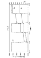
図3Aは、いくつかのシミュレーション結果に従った、従来の高電圧デバイスと開示される高電圧デバイスとの間のターンオン性能を比較するタイミング図を示す。開示される高電圧デバイスは、図1に図示及び記載されるHVD 100を含む。従来の高電圧デバイスは、隔離されたフィールド電極を有さないHEMTを含む高電圧デバイスであり得る。したがって、従来の高電圧デバイスのヘテロ接合レギュレーション電荷拡散手段のすべてが、HEMTの制御ゲートに接続される。HVD 100の電荷拡散手段(例えば、第1及び第2のフィールド電極162及び164)とは異なり、従来の高電圧デバイスの電荷拡散手段は、制御ゲートとの接触を成し、したがって制御ゲートと電荷を共有する。結果として、従来の高電圧デバイスの電荷拡散手段は、制御ゲート関連容量を増加させ、これは、スイッチング時間の増加及びスイッチングの間の電力損失の増大に寄与する。
FIG. 3A shows a timing diagram comparing the turn-on performance between the conventional high voltage device and the disclosed high voltage device according to some simulation results. The disclosed high voltage devices include the
波形302は、ターンオン遷移の間の、従来の高電圧デバイスの過渡VDS電圧を示す。波形304は、ターンオン遷移の間の、開示される高電圧デバイスの過渡VDS電圧(すなわち、HVD 100のドレインノード152とソースノード124の間の電位差)を示す。波形302を波形304と比較すると、開示される高電圧デバイスのターンオン遷移は、従来の高電圧デバイスよりも著しく速い。波形302及び304によって裏付けることにより、波形306は従来の高電圧デバイスの過渡電流IDを示し、波形308は開示される高電圧デバイスの過渡電流IDを示す。波形306を波形308と比較すると、ターンオン遷移の間、開示される高電圧デバイスの過渡電流IDは、従来の高電圧デバイスよりもはるかに速くその飽和レベルに達する。
図3Bは、いくつかのシミュレーション結果に従った、従来の高電圧デバイスと開示される高電圧デバイスとの間のターンオフ性能を比較するタイミング図を示す。開示される高電圧デバイスは、図1に図示及び記載されるHVD 100を含む。従来の高電圧デバイスは、隔離されたフィールド電極を有さないHEMTを含む高電圧デバイスであり得る。したがって、従来の高電圧デバイスのヘテロ接合レギュレーション電荷拡散手段のすべてが、HEMTの制御ゲートに接続される。HVD 100の電荷拡散手段(例えば、第1及び第2のフィールド電極162及び164)とは異なり、従来の高電圧デバイスの電荷拡散手段は、制御ゲートとの接触を成し、したがって制御ゲートと電荷を共有する。結果として、従来の高電圧デバイスの電荷拡散手段は、制御ゲート関連容量を増加させ、これには、スイッチング時間の増加及びスイッチングの間の電力損失の増大に寄与する。
FIG. 3B shows a timing diagram comparing the turn-off performance between the conventional high voltage device and the disclosed high voltage device according to some simulation results. The disclosed high voltage devices include the
波形312は、ターンオフ遷移の間の、従来の高電圧デバイスの過渡VDS電圧を示す。波形314は、ターンオフ遷移の間の、開示される高電圧デバイスの過渡VDS電圧(例えば、HVD 100のドレインノード152とソースノード124の間の電位差)を示す。波形312を波形314と比較すると、開示される高電圧デバイスのターンオフ遷移は、従来の高電圧デバイスよりも著しく速い。波形312及び314によって裏付けることにより、波形316は従来の高電圧デバイスの過渡電流IDを示し、波形318は開示される高電圧デバイスの過渡電流IDを示す。波形316を波形318と比較すると、ターンオフ遷移の間、開示される高電圧デバイスの過渡電流IDは、従来の高電圧デバイスよりもはるかに高速で遮断される。
図4は、図3A及び図3Bにおいて記載されるようなシミュレーション結果に従った、従来の高電圧デバイスと開示される高電圧デバイスとの間のスイッチング電力損失を比較するタイミング図を示す。点線波形401は、従来の高電圧デバイス及び開示される高電圧デバイスの両方に共通の過渡ドレイン・ソース間電圧(VDS)(例えば、HVD 100のノード171と132との間の電圧)を表す。点線波形401が高レベルから低レベルへと遷移するとき、両方のデバイスはターンオンするように構成される。これに対して、点線波形402が低レベルから高レベルへと遷移するとき、両方のデバイスはターンオフするように構成される。
FIG. 4 shows a timing diagram comparing the switching power loss between a conventional high voltage device and a disclosed high voltage device according to the simulation results as described in FIGS. 3A and 3B. Dotted
波形402は、いくつかのスイッチングサイクルにわたる従来の高電圧デバイスの電力消費を示す。波形404は、同じスイッチングサイクルにわたる開示される高電圧デバイスの電力消費を示す。波形402を波形404と比較すると、開示される高電圧デバイスは、各スイッチング遷移(すなわち、ターンオン及びターンオフの両方の遷移)の間、従来の高電圧デバイスよりもはるかに少ない電力損失を維持する。これは、開示される高電圧デバイスが、より高速のスイッチング時間を有し、消費するスイッチング電流がより少量であるという事実に起因する(例えば、図3A及び図3B)。
したがって、例示の実施形態は、電力損失が少なくスイッチング効率が高い高電圧スイッチを含む。例示の実施形態は、低電圧トランジスタ(例えば、シリコンベースの電界効果トランジスタ)を高電圧応用例に適応させるためのマルチ電極制御構造に関するシステム及び技法を含む。開示されるマルチ電極制御構造は、従来の対応する構造よりも高速のターンオン時間及びターンオフ時間を有する。結果として、開示されるマルチ電極制御構造は、スイッチングサイクルの間、より少ない電力損失で高電圧下で動作し得る。 Therefore, an exemplary embodiment includes a high voltage switch with low power loss and high switching efficiency. Illustrative embodiments include systems and techniques for multi-electrode control structures for adapting low voltage transistors (eg, silicon-based field effect transistors) to high voltage applications. The disclosed multi-electrode control structure has faster turn-on and turn-off times than the corresponding conventional structures. As a result, the disclosed multi-electrode control structure can operate under high voltage with less power loss during switching cycles.
一実装において、高電子移動度トランジスタ(HEMT)構造が、基板、2次元電子ガス(2DEG)層、ソースノード、制御ゲート、及びフィールド電極を含む。基板はシリコンの層であり得、その上に2DEG層が配置される。2DEG層は第1の端部及び第2の端部を有し、その両方ともHEMT構造のチャネル領域を横切って延在する。HEMT構造のドレインノードは、2DEG層の第1の端部の上に配置される。対応するソースノードは、2DEG層の第1と第2の端部間にドレインノードとのチャネルを画定するために、2DEG層の第2の端部の上に配置される。したがって、ソースノードは、ドレインノードとのドレイン・ソース容量(CDS)を確立する。HEMT構造の制御ゲートは、チャネルの上に配置され、ゲート・ソース電圧に応答してチャネルに沿って電荷を集結するように構成される。制御ゲートは、ソースノードとのゲート・ソース容量(CGS)、及びドレインノードとのゲート・ドレイン容量(CGD)を確立する。HEMT構造のフィールド電極は、チャネルの上に配置され、集結された電荷をフィールド電圧に応答して拡散するように構成される。フィールド電極は、ドレインノード、ソースノード、又は制御ゲートのうちのいずれの一つとも電荷を共有することを防ぐように、構造化及び配路される。例えば、フィールド電極は、制御ゲート、ドレインノード、及びソースノードから構造的及び電気的に隔離される。有利なことに、フィールド電極は、容量CDS、CGD、及びCGSを維持するように構造化及び配路されて、HEMT構造が、より少ない電力損失及びよりロバストな性能でスイッチし得るようになっている。In one implementation, the high electron mobility transistor (HEMT) structure includes a substrate, a two-dimensional electron gas (2DEG) layer, a source node, a control gate, and a field electrode. The substrate can be a layer of silicon on which a 2DEG layer is placed. The 2DEG layer has a first end and a second end, both of which extend across the channel region of the HEMT structure. The drain node of the HEMT structure is placed on the first end of the 2DEG layer. The corresponding source node is placed above the second end of the 2DEG layer to define a channel with the drain node between the first and second ends of the 2DEG layer. Therefore, the source node establishes a drain source capacity (CDS) with the drain node. The control gate of the HEMT structure is formed above a channel, configured to condense forming the charge along the channel in response to the gate-source voltage. The control gate establishes a gate-source capacity ( CGS ) with the source node and a gate-drain capacity ( CGD ) with the drain node. Field electrode of the HEMT structure is formed above a channel, and a converging forming charge to diffuse in response to the field voltage. The field electrodes are structured and routed to prevent sharing charge with any one of the drain node, source node, or control gate. For example, field electrodes are structurally and electrically isolated from control gates, drain nodes, and source nodes. Advantageously, as the field electrode, capacitor C DS, it is structured and Jairo to maintain the C GD, and C GS, HEMT structures may switch with less power loss and a more robust performance It has become.
別の実装において、高電圧スイッチが、高電圧トランジスタ(HVT)、及び、HVTとカスコード構造を形成する低電圧トランジスタ(LVT)を含む。HVTは、高電圧源を受け取るように構成されるドレインノード、及び、ドレインノードと高電圧チャネルを画定するように構成されるソースノードを含む。また、HVTは、ドレインノードとソースノードとの間に置かれる制御ゲートを含み、制御ゲートはチャネルをレギュレートするように構成される。HVTは、チャネルの上に配置されるフィールド電極を更に含む。フィールド電極もチャネルを再レギュレートするように構成されるが、フィールド電極は制御ゲートから隔離される。したがって、フィールド電極は、ドレインノード、ソースノード、又は制御ゲートのうちのいずれの一つとも電荷を共有することを防ぐように、構造化及び配路される。有利なことに、高電圧スイッチは、わずかな電力損失及び短いスイッチング時間で高電圧下で動作し得る。 In another implementation, the high voltage switch comprises a high voltage transistor (HVT) and a low voltage transistor (LVT) that forms a cascode structure with the HVT. The HVT includes a drain node configured to receive a high voltage source and a source node configured to define the drain node and the high voltage channel. The HVT also includes a control gate located between the drain node and the source node, which is configured to regulate the channel. The HVT further includes a field electrode located above the channel. The field electrode is also configured to re-regulate the channel, but the field electrode is isolated from the control gate. Therefore, the field electrodes are structured and routed to prevent sharing charge with any one of the drain node, source node, or control gate. Advantageously, the high voltage switch can operate under high voltage with little power loss and short switching time.
更に別の実装において、高電圧デバイスが、高電子移動度トランジスタ(HEMT)とカスコード構成を形成する低電圧トランジスタ(LVT)を含む。LVTは、第1の基板上に形成され、第1のドレインノード、第1の制御ゲート、及び第1のソースノードを有する。HEMTは第2の基板上に形成され、第2の基板は、第1の基板から物理的に分離された基板、又は、第1の基板と共有される共通基板の領域であり得る。HEMTは、2次元電子ガス(2DEG)層、第2のドレインノード、第2のソースノード、第2の制御ゲート、及びフィールド電極を含む。2DEG層は第2の基板の上に配置される。第2のドレインノードは、2DEG層の上に配置され、高電圧源を受け取るように構成される。第2のソースノードは、2DEG層の上に配置され、LVTの第1のドレインノードと接続される。第2の制御ゲートは、2DEG層の上に配置され、第2のドレインノード、第2のソースノード、及び2DEG層によって連帯的に画定されるチャネルをレギュレートするように構成される。フィールド電極は、チャネルの上に配置され、チャネルに沿って電荷を分布させるように構成される。フィールド電極は、第2の基板によって画定される領域にわたって、第2の制御ゲート、第2のドレインノード、及び第2のソースノードとは接していないため、第2の制御ゲートに追加の容量負荷を負わせることはない。有利なことに、高電圧デバイスは、わずかな電力損失及び短いスイッチング時間で高電圧下でスイッチし得る。 In yet another implementation, the high voltage device includes a high electron mobility transistor (HEMT) and a low voltage transistor (LVT) that forms a cascode configuration. The LVT is formed on a first substrate and has a first drain node, a first control gate, and a first source node. The HEMT may be formed on a second substrate, and the second substrate may be a substrate physically separated from the first substrate or a region of a common substrate shared with the first substrate. The HEMT includes a two-dimensional electron gas (2DEG) layer, a second drain node, a second source node, a second control gate, and a field electrode. The 2DEG layer is placed on top of the second substrate. The second drain node is located on top of the 2DEG layer and is configured to receive a high voltage source. The second source node is located above the 2DEG layer and is connected to the first drain node of the LVT. The second control gate is located above the 2DEG layer and is configured to regulate the channels jointly defined by the second drain node, the second source node, and the 2DEG layer. The field electrodes are placed on top of the channel and are configured to distribute charge along the channel. Since the field electrode is not in contact with the second control gate, the second drain node, and the second source node over the region defined by the second substrate, an additional capacitive load is applied to the second control gate. Do not impose. Advantageously, high voltage devices can switch under high voltage with little power loss and short switching time.
本明細書において記載される機能的動作を含むシステム及び技法は、説明される方法及び/又は動作を一つ又は複数のデータ処理装置に行わせるように動作可能なプログラム(例えば、メモリデバイス、ストレージデバイス、機械可読ストレージ基板、又は他の物理的機械可読媒体、或いはそれらの一つ又は複数の組み合わせであり得る、コンピュータ可読媒体に符号化されるプログラムなど)を潜在的に含む、本明細書において開示される構造的手段及びそれらの構造的等価物などの、電子回路、コンピュータハードウェア、ファームウェア、ソフトウェア、又はそれらの組み合わせにおいて実装され得る。 The systems and techniques including the functional operations described herein are programs (eg, memory devices, storage) capable of operating to cause one or more data processing devices to perform the methods and / or operations described. As used herein, it potentially includes a device, a machine-readable storage board, or other physical machine-readable medium, or a program encoded on a computer-readable medium, which may be one or more combinations thereof. It can be implemented in electronic circuits, computer hardware, firmware, software, or a combination thereof, such as the disclosed structural means and their structural equivalents.
デバイスは、そのデバイスが、或る機能を行なうためにイネーブルされ、活性化され、又は電力供給され得る有形の非一時的構成要素をデバイスが含む場合、その機能を行なう「ように構成される」。デバイスを説明する際の「するように構成される」という用語は、そのデバイスがいかなる所与の時点でも構成可能であることを要求しない。 A device is "configured" to perform a function if the device contains tangible non-temporary components that may be enabled, activated, or powered to perform that function. .. The term "configured to" in describing a device does not require that the device be configurable at any given time point.
たとえ或る特徴が、別個の実施形態の文脈において本明細書に記載される場合でも、そういった特徴は単一の実施形態において組み合わせて実装され得る。逆に、たとえ様々の特徴が単一の実施形態の文脈において記載される場合でも、そういった特徴は複数の実施形態において別個に、又は任意の適切な副次的組み合わせで、実装され得る。また、たとえ上記で幾つかの特徴が或る組み合わせで機能するように記載される場合でも、それらの特徴の一つ又は複数が(少なくともいくつかの場合において)、その組み合わせから除かれ得、そういった組み合わせは、それらの副次的組み合わせ又は変形に分割され得る。 Even if certain features are described herein in the context of separate embodiments, such features can be implemented in combination in a single embodiment. Conversely, even if the various features are described in the context of a single embodiment, they may be implemented separately in multiple embodiments or in any suitable secondary combination. Also, even if some features are described above to work in a combination, one or more of those features (in at least some cases) may be excluded from that combination, such. Combinations can be divided into their secondary combinations or variants.
同様に、動作が、図面において特定の順で示されているが、こうした動作は、異なる順で又は不順次的に成され得、動作の一つ又は複数が任意選択であり得る。例えば、マルチタスク及び並列処理が有利であり得る。また、たとえいくつかの実施形態において様々のシステム構成要素が分離されている場合でも、それらの構成要素は他の実施形態において一体であり得る。 Similarly, the actions are shown in the drawings in a particular order, but these actions may be performed in a different order or in a random order, and one or more of the actions may be optional. For example, multitasking and parallel processing can be advantageous. Also, even if the various system components are separated in some embodiments, those components can be integrated in other embodiments.
Claims (14)
第1の基板上に形成され、第1のドレインノードと第1の制御ゲートと第1のソースノードとを含む低電圧トランジスタ(LVT)と、
第2の基板上に形成される高電子移動度トランジスタ(HEMT)であって、
前記第2の基板の上に配置される2次元電子ガス(2DEG)層と、
前記2DEG層の上に配置され、高電圧源を受け取るように構成される第2のドレインノードと、
前記2DEG層の上に配置され、前記LVTの前記第1のドレインノードと接続される第2のソースノードと、
前記2DEG層の上に配置され、前記第2のドレインノードと前記第2のソースノードと前記2DEG層とによって連帯的に画定されるチャネルをレギュレートするように構成される第2の制御ゲートと、
前記チャネルの上に配置され、前記チャネルに沿って電荷を分布させるように構成されるフィールド電極であって、前記第2の制御ゲートと前記第2のソースノードとに電気的に結合されていない、前記フィールド電極と、
を含む、前記HEMTと、
前記HEMTのフィールド電極を前記LVTの第1のソースノードに接続する第1のボンディングワイヤと、
前記HEMTの第2の制御ゲートを前記LVTの第1のソースノードに接続し、前記第1のボンディングワイヤから分離されている第2のボンディングワイヤと、
を含む、高電圧デバイス。High voltage device
A low voltage transistor (LVT) formed on a first substrate and including a first drain node, a first control gate, and a first source node.
A high electron mobility transistor (HEMT) formed on a second substrate.
A two-dimensional electron gas (2DEG) layer arranged on the second substrate,
A second drain node located on the 2DEG layer and configured to receive a high voltage source,
A second source node arranged on the 2DEG layer and connected to the first drain node of the LVT, and
A second control gate that is located on top of the 2DEG layer and is configured to regulate channels that are jointly defined by the second drain node, the second source node, and the 2DEG layer. ,
Disposed over the channel, a field electrode configured to distribute electric charge along the channel, it is not electrically coupled to said second control gate and said second source node , The field electrode and
Including the HEMT and
A first bonding wire that connects the HEMT field electrode to the first source node of the LVT, and
A second bonding wire that connects the second control gate of the HEMT to the first source node of the LVT and is separated from the first bonding wire, and
Including high voltage devices.
前記フィールド電極が、前記第2の制御ゲートよりも前記2DEG層からより遠くに位置する、高電圧デバイス。 The high voltage device according to claim 1.
Wherein the field electrode is located farther from the 2DEG layer than the second control gate, high voltage devices.
前記第2の基板の上に形成され、前記HEMTの前記フィールド電極と接続される第1のボンディングパッドと、
前記第2の基板の上に形成され、前記第1のボンディングパッドから分離される第2のボンディングパッドであって、前記HEMTの第2の制御ゲートと接続される、前記第2のボンディングパッドと、
前記第2の基板の上に形成され、前記第1のボンディングパッドから分離される第3のボンディングパッドであって、前記HEMTの第2のソースノードと接続される、前記第3のボンディングパッドと、
を更に含む、高電圧デバイス。 The high voltage device according to claim 1.
A first bonding pad formed on the second substrate and connected to the field electrode of the HEMT, and a first bonding pad.
Formed on the second substrate, a second bonding pad that is separated from the first bonding pad is connected to the second control gate of the HEMT, and the second bonding pads ,
A third bonding pad formed on the second substrate and separated from the first bonding pad, which is connected to the second source node of the HEMT and the third bonding pad . ,
High voltage devices, including further.
前記LVTの前記第1のソースノードがソース電圧を受け取るように構成される、高電圧デバイス。 The high voltage device according to claim 1.
A high voltage device configured such that the first source node of the LVT receives a source voltage.
前記HEMTの前記フィールド電極を前記LVTの前記第1のソースノードに接続する第1のリンギング抑制器であって、前記第1のボンディングワイヤと直列である、前記第1のリンギング抑制器と、
前記HEMTの前記第2の制御ゲートを前記LVTの前記第1のソースノードに接続する第2のリンギング抑制器であって、前記第2のボンディングワイヤと直列であり、前記第1のリンギング抑制器から電気的に独立している、前記第2のリンギング抑制器と、
を更に含む、高電圧デバイス。 The high voltage device according to claim 4.
A first ringing suppressor that connects the field electrode of the HEMT to the first source node of the LVT, the first ringing suppressor that is in series with the first bonding wire .
A second ringing suppressor for connecting the second control gate of the HEMT in the first source node of the LVT, the a second bonding wire in series, the first ringing suppressor electrically that independent, the second ringing suppressor from
High voltage devices , including further.
前記HEMTの前記第2の制御ゲートが前記チャネルをレギュレートするために第1の電圧を受け取るように構成され、
前記HEMTの前記フィールド電極が前記第1の電圧とは異なる第2の電圧を受け取るように構成され、前記第2の電圧が前記チャネルに沿って前記電荷を分布させるためのものである、高電圧デバイス。 The high voltage device according to claim 1.
The second control gate of the HEMT is configured to receive a first voltage to regulate the channel.
The field electrode of the HEMT is configured to receive a second voltage different from the first voltage, the second voltage is for distributing the charge along the channel, a high voltage. device.
前記HEMTの前記フィールド電極が、
前記チャネルの第1の領域の上に配置され、前記第2の制御ゲートと接していない第1のフィールド電極であって、前記チャネルの前記第1の領域における電荷を分布させるように構成される、前記第1のフィールド電極と、
前記第1のフィールド電極から分離される第2のフィールド電極であって、前記チャネルの第2の領域の上に配置され、前記第2の制御ゲートと接しておらず、前記チャネルの前記第2の領域における電荷を分布させるように構成される、前記第2のフィールド電極と、
を含む、高電圧デバイス。 The high voltage device according to claim 1.
The field electrode of the HEMT
A first field electrode located above the first region of the channel and not in contact with the second control gate, configured to distribute charges in the first region of the channel. , The first field electrode and
A second field electrode separated from the first field electrode, located above the second region of the channel, not in contact with the second control gate, and the second of the channel. The second field electrode, which is configured to distribute the charge in the region of
Including high voltage devices.
前記第1の基板が前記第2の基板から分離する、高電圧デバイス。 The high voltage device according to claim 1.
A high voltage device in which the first substrate is separated from the second substrate.
前記第1の基板が共通基板上のLVT領域を占有し、
前記第2の基板が前記共通基板上のHEMT領域を占有する、高電圧デバイス。 The high voltage device according to claim 1.
The first substrate occupies the LVT region on the common substrate,
A high voltage device in which the second substrate occupies a HEMT region on the common substrate.
高電圧トランジスタ(HVT)であって、
高電圧源を受け取るように構成されるドレインノードと、
前記ドレインノードと高電圧チャネルを画定するように構成されるソースノードと、
前記ドレインノードと前記ソースノードとの間に置かれる制御ゲートであって、前記高電圧チャネルをレギュレートするように構成される前記制御ゲートと、
前記高電圧チャネルの上に配置され、前記高電圧チャネルを再レギュレートするように構成されるフィールド電極であって、前記HVT内で前記ドレインノードと前記ソースノードと前記制御ゲートとから隔離される、前記フィールド電極と、
を含む、前記HVTと、
低電圧トランジスタ(LVT)であって、
前記HVTの前記ソースノードと結合され、出力電圧を搬送するように構成されるドレインノードと、
ソース電圧を受け取るように構成されるソースノードと、
前記HVTの前記制御ゲートと前記HVTの前記ソースノードとの間の電位差を調節
することによって、入力電圧に応答して前記出力電圧を制御するように構成される、制御ゲートと、
を含む、前記LVTと、
前記HVTの前記フィールド電極を前記LVTの前記ソースノードに接続する第1のボンディングワイヤと、
前記HVTの前記制御ゲートを前記LVTの前記ソースノードに接続し、前記第1のボンディングワイヤから分離される第2のボンディングワイヤと、
を含む、高電圧スイッチ。 It ’s a high voltage switch,
A high-voltage transistors (HVT),
With a drain node configured to receive a high voltage source,
A source node configured to demarcate the drain node and the high voltage channel,
A control gate placed between the drain node and the source node, the control gate configured to regulate the high voltage channel, and the control gate.
A field electrode located above the high voltage channel and configured to reregulate the high voltage channel, isolated from the drain node , the source node, and the control gate within the HVT. , The field electrode and
Including the HVT and
It is a low voltage transistor ( LVT )
A drain node coupled with the source node of the HVT and configured to carry an output voltage.
With a source node configured to receive the source voltage,
A control gate configured to control the output voltage in response to an input voltage by adjusting the potential difference between the control gate of the HVT and the source node of the HVT.
With the above LVT including
A first bonding wire that connects the field electrode of the HVT to the source node of the LVT, and
A second bonding wire that connects the control gate of the HVT to the source node of the LVT and is separated from the first bonding wire.
Including high voltage switch.
前記HVTの前記フィールド電極を前記LVTの前記ソースノードに接続する第1のリンギング抑制器であって、前記第1のボンディングワイヤと直列である、前記第1のリンギング抑制器と、
前記HVTの前記制御ゲートを前記LVTの前記ソースノードに接続する第2のリンギング抑制器であって、前記第2のボンディングワイヤと直列であり、前記第1のリンギング抑制器から電気的に独立している、前記第2のリンギング抑制器と、
を更に含む、高電圧スイッチ。 The high voltage switch according to claim 10.
A first ringing suppressor that connects the field electrode of the HVT to the source node of the LVT, and the first ringing suppressor that is in series with the first bonding wire .
A second ringing suppressor for connecting the control gates of the HVT to the source node of the LVT, the a second bonding wire series, electrically independent from the first ringing suppressor Tei Ru, and said second ringing suppressor,
Including, high voltage switch.
前記HVTの前記フィールド電極が、前記HVTによって画定される領域にわたって、前記HVTの前記ドレインノードとソースノードと制御ゲートとのうちのいずれの1つとも接していない、高電圧スイッチ。 The high voltage switch according to claim 10.
Wherein said field electrodes HVT is over a region defined by said HVT, not in contact with the at any one of one of said drain and source nodes and the control gate of the HVT, a high voltage switch.
前記HVTの前記制御ゲートが前記高電圧チャネルに沿って電荷を集結させるために第1の電圧を受け取るように構成され、
前記HVTの前記フィールド電極が前記第1の電圧とは異なる第2の電圧を受け取るように構成され、前記第2の電圧が前記集結された電荷を前記高電圧チャネルに沿って拡散するためのものである、高電圧スイッチ。The high voltage switch according to claim 10.
Configured to receive a first voltage to said control gate of said HVT can be condensed forming the charge along the high voltage channel,
Wherein configured to receive a second voltage different from said field electrode is the first voltage of HVT, the second voltage to spread along the collector forming the charge on the high voltage channel A high voltage switch that is a thing.
前記HVTの前記フィールド電極が、
前記高電圧チャネルの第1の領域の上に配置され、前記高電圧チャネルの前記第1の領域における電荷を分布させるように構成される第1のフィールド電極と、
前記第1のフィールド電極から分離され、前記高電圧チャネルの第2の領域の上に配置され、前記高電圧チャネルの前記第2の領域における電荷を分布させるように構成される第2のフィールド電極と、
を含む、高電圧スイッチ。 The high voltage switch according to claim 10.
The field electrode of the HVT is
A first is arranged above the region, the high voltage channels the first of the first configured to distribute charge in the area of the field electrode of the high voltage channel,
A second field electrode separated from the first field electrode, placed on top of a second region of the high voltage channel, and configured to distribute charges in the second region of the high voltage channel. And
Including high voltage switch.
Applications Claiming Priority (3)
| Application Number | Priority Date | Filing Date | Title |
|---|---|---|---|
| US14/747,169 | 2015-06-23 | ||
| US14/747,169 US9991225B2 (en) | 2015-06-23 | 2015-06-23 | High voltage device with multi-electrode control |
| PCT/US2016/038727 WO2016209934A1 (en) | 2015-06-23 | 2016-06-22 | High voltage device with multi-electrode control |
Publications (3)
| Publication Number | Publication Date |
|---|---|
| JP2018524813A JP2018524813A (en) | 2018-08-30 |
| JP2018524813A5 JP2018524813A5 (en) | 2019-07-11 |
| JP6903833B2 true JP6903833B2 (en) | 2021-07-14 |
Family
ID=57585634
Family Applications (1)
| Application Number | Title | Priority Date | Filing Date |
|---|---|---|---|
| JP2017567057A Active JP6903833B2 (en) | 2015-06-23 | 2016-06-22 | High voltage device with multi-electrode control |
Country Status (4)
| Country | Link |
|---|---|
| US (2) | US9991225B2 (en) |
| JP (1) | JP6903833B2 (en) |
| CN (2) | CN107924918B (en) |
| WO (1) | WO2016209934A1 (en) |
Families Citing this family (5)
| Publication number | Priority date | Publication date | Assignee | Title |
|---|---|---|---|---|
| US9991225B2 (en) * | 2015-06-23 | 2018-06-05 | Texas Instruments Incorporated | High voltage device with multi-electrode control |
| DE102017100614B4 (en) * | 2017-01-13 | 2021-11-25 | Infineon Technologies Austria Ag | Semiconductor device comprising a transistor and a conductive plate |
| CN114823888A (en) * | 2021-01-22 | 2022-07-29 | 联华电子股份有限公司 | High electron mobility transistor and manufacturing method thereof |
| EP4044225B1 (en) * | 2021-02-16 | 2024-06-26 | Nexperia B.V. | A semiconductor device and a method of manufacturing a semiconductor device |
| US20240204764A1 (en) * | 2022-12-14 | 2024-06-20 | Globalfoundries U.S. Inc. | High voltage device with linearizing field plate configuration |
Family Cites Families (20)
| Publication number | Priority date | Publication date | Assignee | Title |
|---|---|---|---|---|
| JP3259106B2 (en) | 1992-09-02 | 2002-02-25 | 富士通株式会社 | High electron mobility field effect semiconductor device |
| JP2001319490A (en) | 2000-05-12 | 2001-11-16 | Mitsubishi Electric Corp | High voltage switch circuit, and semiconductor memory provided with high voltage switch circuit |
| US7161194B2 (en) * | 2004-12-06 | 2007-01-09 | Cree, Inc. | High power density and/or linearity transistors |
| KR100782430B1 (en) * | 2006-09-22 | 2007-12-05 | 한국과학기술원 | Gan-hemt (high electron mobility transistor) structure with inner field-plate structure for high power applications |
| WO2011100304A1 (en) * | 2010-02-09 | 2011-08-18 | Massachusetts Institute Of Technology | Dual-gate normally-off nitride transistors |
| JP2012049962A (en) * | 2010-08-30 | 2012-03-08 | Toshiba Corp | Semiconductor switch circuit |
| US8860120B2 (en) * | 2010-09-22 | 2014-10-14 | Nxp, B.V. | Field modulating plate and circuit |
| US8680627B2 (en) | 2011-01-14 | 2014-03-25 | International Rectifier Corporation | Stacked half-bridge package with a common conductive clip |
| JP5866773B2 (en) * | 2011-02-25 | 2016-02-17 | 富士通株式会社 | Compound semiconductor device and manufacturing method thereof |
| JP2013074070A (en) * | 2011-09-27 | 2013-04-22 | Fujitsu Ltd | Semiconductor device and manufacturing method of semiconductor device |
| US9312347B2 (en) * | 2011-11-21 | 2016-04-12 | Sensor Electronic Technology, Inc. | Semiconductor device with multiple space-charge control electrodes |
| US8624667B2 (en) | 2011-12-05 | 2014-01-07 | Mitsubishi Electric Research Laboratories, Inc. | High electron mobility transistors with multiple channels |
| JP6075003B2 (en) * | 2012-10-22 | 2017-02-08 | 富士通株式会社 | Transistor control circuit and power supply device |
| US20140225163A1 (en) * | 2013-02-11 | 2014-08-14 | International Rectifier Corporation | Inverter Circuit Including Short Circuit Protected Composite Switch |
| JP2014229823A (en) * | 2013-05-24 | 2014-12-08 | 古河電気工業株式会社 | Semiconductor device and semiconductor module |
| JP6240460B2 (en) * | 2013-10-02 | 2017-11-29 | トランスフォーム・ジャパン株式会社 | Field effect type compound semiconductor device and manufacturing method thereof |
| EP3080845B1 (en) | 2013-11-15 | 2021-12-22 | Texas Instruments Incorporated | Method and circuitry for controlling a depletion-mode transistor |
| US9343562B2 (en) * | 2013-12-06 | 2016-05-17 | Infineon Technologies Americas Corp. | Dual-gated group III-V merged transistor |
| US9325308B2 (en) * | 2014-05-30 | 2016-04-26 | Delta Electronics, Inc. | Semiconductor device and cascode circuit |
| US9991225B2 (en) * | 2015-06-23 | 2018-06-05 | Texas Instruments Incorporated | High voltage device with multi-electrode control |
-
2015
- 2015-06-23 US US14/747,169 patent/US9991225B2/en active Active
-
2016
- 2016-06-22 JP JP2017567057A patent/JP6903833B2/en active Active
- 2016-06-22 CN CN201680036699.4A patent/CN107924918B/en active Active
- 2016-06-22 CN CN202111298536.2A patent/CN114023741A/en active Pending
- 2016-06-22 WO PCT/US2016/038727 patent/WO2016209934A1/en active Application Filing
-
2018
- 2018-04-06 US US15/947,227 patent/US10340252B2/en active Active
Also Published As
| Publication number | Publication date |
|---|---|
| WO2016209934A8 (en) | 2018-03-01 |
| US10340252B2 (en) | 2019-07-02 |
| US9991225B2 (en) | 2018-06-05 |
| CN107924918A (en) | 2018-04-17 |
| US20180233481A1 (en) | 2018-08-16 |
| CN114023741A (en) | 2022-02-08 |
| WO2016209934A1 (en) | 2016-12-29 |
| US20160380089A1 (en) | 2016-12-29 |
| JP2018524813A (en) | 2018-08-30 |
| CN107924918B (en) | 2021-11-26 |
Similar Documents
| Publication | Publication Date | Title |
|---|---|---|
| JP6903833B2 (en) | High voltage device with multi-electrode control | |
| US9007117B2 (en) | Solid-state switching device having a high-voltage switching transistor and a low-voltage driver transistor | |
| KR102198021B1 (en) | Compact electrostatic discharge (esd) protection structure | |
| US9966945B2 (en) | Semiconductor device | |
| US11005453B2 (en) | Dynamic high voltage (HV) level shifter with temperature compensation for high-side gate driver | |
| US20110316045A1 (en) | LAYOUT DESIGN FOR A HIGH POWER, GaN-BASED FET | |
| JP5285103B2 (en) | Nitride semiconductor device | |
| US10679987B2 (en) | Bootstrap metal-oxide-semiconductor (MOS) device integrated with a high voltage MOS (HVMOS) device and a high voltage junction termination (HVJT) device | |
| US9331572B2 (en) | Semiconductor device and power conversion device | |
| US20160247792A1 (en) | Switch circuit of cascode type having high speed switching performance | |
| US10050034B2 (en) | Semiconductor device and associated methods | |
| US11296601B2 (en) | Power transistor with distributed gate | |
| US9123796B2 (en) | Semiconductor device | |
| US10630285B1 (en) | Switching circuits having drain connected ferrite beads | |
| US9324819B1 (en) | Semiconductor device | |
| US9646965B2 (en) | Monolithically integrated transistors for a buck converter using source down MOSFET | |
| CN106373996B (en) | Semiconductor device with a plurality of semiconductor chips | |
| US9325308B2 (en) | Semiconductor device and cascode circuit | |
| CN108735730B (en) | Power switch and semiconductor device thereof | |
| JP2016174240A (en) | Semiconductor switch | |
| Würfl et al. | Enabling GaN high speed devices: Microwave meets power electronics-And vice versa | |
| CN105684136A (en) | Semiconductor device |
Legal Events
| Date | Code | Title | Description |
|---|---|---|---|
| A521 | Request for written amendment filed |
Free format text: JAPANESE INTERMEDIATE CODE: A821 Effective date: 20171225 |
|
| A521 | Request for written amendment filed |
Free format text: JAPANESE INTERMEDIATE CODE: A523 Effective date: 20190604 |
|
| A621 | Written request for application examination |
Free format text: JAPANESE INTERMEDIATE CODE: A621 Effective date: 20190604 |
|
| A131 | Notification of reasons for refusal |
Free format text: JAPANESE INTERMEDIATE CODE: A131 Effective date: 20200701 |
|
| A521 | Request for written amendment filed |
Free format text: JAPANESE INTERMEDIATE CODE: A523 Effective date: 20200925 |
|
| TRDD | Decision of grant or rejection written | ||
| A01 | Written decision to grant a patent or to grant a registration (utility model) |
Free format text: JAPANESE INTERMEDIATE CODE: A01 Effective date: 20210203 |
|
| A711 | Notification of change in applicant |
Free format text: JAPANESE INTERMEDIATE CODE: A711 Effective date: 20210218 |
|
| A61 | First payment of annual fees (during grant procedure) |
Free format text: JAPANESE INTERMEDIATE CODE: A61 Effective date: 20210222 |
|
| A521 | Request for written amendment filed |
Free format text: JAPANESE INTERMEDIATE CODE: A523 Effective date: 20210323 |
|
| A521 | Request for written amendment filed |
Free format text: JAPANESE INTERMEDIATE CODE: A523 Effective date: 20210602 |
|
| R150 | Certificate of patent or registration of utility model |
Ref document number: 6903833 Country of ref document: JP Free format text: JAPANESE INTERMEDIATE CODE: R150 |
|
| R250 | Receipt of annual fees |
Free format text: JAPANESE INTERMEDIATE CODE: R250 |