JP6903061B2 - Plating process and chemistry of through silicon vias - Google Patents
Plating process and chemistry of through silicon vias Download PDFInfo
- Publication number
- JP6903061B2 JP6903061B2 JP2018537774A JP2018537774A JP6903061B2 JP 6903061 B2 JP6903061 B2 JP 6903061B2 JP 2018537774 A JP2018537774 A JP 2018537774A JP 2018537774 A JP2018537774 A JP 2018537774A JP 6903061 B2 JP6903061 B2 JP 6903061B2
- Authority
- JP
- Japan
- Prior art keywords
- layer
- silicon substrate
- metal
- feature
- exposing
- Prior art date
- Legal status (The legal status is an assumption and is not a legal conclusion. Google has not performed a legal analysis and makes no representation as to the accuracy of the status listed.)
- Active
Links
Images


Classifications
-
- H—ELECTRICITY
- H01—ELECTRIC ELEMENTS
- H01L—SEMICONDUCTOR DEVICES NOT COVERED BY CLASS H10
- H01L21/00—Processes or apparatus adapted for the manufacture or treatment of semiconductor or solid state devices or of parts thereof
- H01L21/70—Manufacture or treatment of devices consisting of a plurality of solid state components formed in or on a common substrate or of parts thereof; Manufacture of integrated circuit devices or of parts thereof
- H01L21/71—Manufacture of specific parts of devices defined in group H01L21/70
- H01L21/768—Applying interconnections to be used for carrying current between separate components within a device comprising conductors and dielectrics
- H01L21/76838—Applying interconnections to be used for carrying current between separate components within a device comprising conductors and dielectrics characterised by the formation and the after-treatment of the conductors
- H01L21/76841—Barrier, adhesion or liner layers
- H01L21/76871—Layers specifically deposited to enhance or enable the nucleation of further layers, i.e. seed layers
- H01L21/76873—Layers specifically deposited to enhance or enable the nucleation of further layers, i.e. seed layers for electroplating
-
- C—CHEMISTRY; METALLURGY
- C23—COATING METALLIC MATERIAL; COATING MATERIAL WITH METALLIC MATERIAL; CHEMICAL SURFACE TREATMENT; DIFFUSION TREATMENT OF METALLIC MATERIAL; COATING BY VACUUM EVAPORATION, BY SPUTTERING, BY ION IMPLANTATION OR BY CHEMICAL VAPOUR DEPOSITION, IN GENERAL; INHIBITING CORROSION OF METALLIC MATERIAL OR INCRUSTATION IN GENERAL
- C23C—COATING METALLIC MATERIAL; COATING MATERIAL WITH METALLIC MATERIAL; SURFACE TREATMENT OF METALLIC MATERIAL BY DIFFUSION INTO THE SURFACE, BY CHEMICAL CONVERSION OR SUBSTITUTION; COATING BY VACUUM EVAPORATION, BY SPUTTERING, BY ION IMPLANTATION OR BY CHEMICAL VAPOUR DEPOSITION, IN GENERAL
- C23C16/00—Chemical coating by decomposition of gaseous compounds, without leaving reaction products of surface material in the coating, i.e. chemical vapour deposition [CVD] processes
- C23C16/22—Chemical coating by decomposition of gaseous compounds, without leaving reaction products of surface material in the coating, i.e. chemical vapour deposition [CVD] processes characterised by the deposition of inorganic material, other than metallic material
- C23C16/30—Deposition of compounds, mixtures or solid solutions, e.g. borides, carbides, nitrides
- C23C16/40—Oxides
- C23C16/401—Oxides containing silicon
-
- C—CHEMISTRY; METALLURGY
- C23—COATING METALLIC MATERIAL; COATING MATERIAL WITH METALLIC MATERIAL; CHEMICAL SURFACE TREATMENT; DIFFUSION TREATMENT OF METALLIC MATERIAL; COATING BY VACUUM EVAPORATION, BY SPUTTERING, BY ION IMPLANTATION OR BY CHEMICAL VAPOUR DEPOSITION, IN GENERAL; INHIBITING CORROSION OF METALLIC MATERIAL OR INCRUSTATION IN GENERAL
- C23C—COATING METALLIC MATERIAL; COATING MATERIAL WITH METALLIC MATERIAL; SURFACE TREATMENT OF METALLIC MATERIAL BY DIFFUSION INTO THE SURFACE, BY CHEMICAL CONVERSION OR SUBSTITUTION; COATING BY VACUUM EVAPORATION, BY SPUTTERING, BY ION IMPLANTATION OR BY CHEMICAL VAPOUR DEPOSITION, IN GENERAL
- C23C18/00—Chemical coating by decomposition of either liquid compounds or solutions of the coating forming compounds, without leaving reaction products of surface material in the coating; Contact plating
- C23C18/16—Chemical coating by decomposition of either liquid compounds or solutions of the coating forming compounds, without leaving reaction products of surface material in the coating; Contact plating by reduction or substitution, e.g. electroless plating
- C23C18/1601—Process or apparatus
- C23C18/1633—Process of electroless plating
- C23C18/1646—Characteristics of the product obtained
- C23C18/165—Multilayered product
- C23C18/1653—Two or more layers with at least one layer obtained by electroless plating and one layer obtained by electroplating
-
- C—CHEMISTRY; METALLURGY
- C23—COATING METALLIC MATERIAL; COATING MATERIAL WITH METALLIC MATERIAL; CHEMICAL SURFACE TREATMENT; DIFFUSION TREATMENT OF METALLIC MATERIAL; COATING BY VACUUM EVAPORATION, BY SPUTTERING, BY ION IMPLANTATION OR BY CHEMICAL VAPOUR DEPOSITION, IN GENERAL; INHIBITING CORROSION OF METALLIC MATERIAL OR INCRUSTATION IN GENERAL
- C23C—COATING METALLIC MATERIAL; COATING MATERIAL WITH METALLIC MATERIAL; SURFACE TREATMENT OF METALLIC MATERIAL BY DIFFUSION INTO THE SURFACE, BY CHEMICAL CONVERSION OR SUBSTITUTION; COATING BY VACUUM EVAPORATION, BY SPUTTERING, BY ION IMPLANTATION OR BY CHEMICAL VAPOUR DEPOSITION, IN GENERAL
- C23C28/00—Coating for obtaining at least two superposed coatings either by methods not provided for in a single one of groups C23C2/00 - C23C26/00 or by combinations of methods provided for in subclasses C23C and C25C or C25D
- C23C28/30—Coatings combining at least one metallic layer and at least one inorganic non-metallic layer
- C23C28/32—Coatings combining at least one metallic layer and at least one inorganic non-metallic layer including at least one pure metallic layer
-
- C—CHEMISTRY; METALLURGY
- C23—COATING METALLIC MATERIAL; COATING MATERIAL WITH METALLIC MATERIAL; CHEMICAL SURFACE TREATMENT; DIFFUSION TREATMENT OF METALLIC MATERIAL; COATING BY VACUUM EVAPORATION, BY SPUTTERING, BY ION IMPLANTATION OR BY CHEMICAL VAPOUR DEPOSITION, IN GENERAL; INHIBITING CORROSION OF METALLIC MATERIAL OR INCRUSTATION IN GENERAL
- C23C—COATING METALLIC MATERIAL; COATING MATERIAL WITH METALLIC MATERIAL; SURFACE TREATMENT OF METALLIC MATERIAL BY DIFFUSION INTO THE SURFACE, BY CHEMICAL CONVERSION OR SUBSTITUTION; COATING BY VACUUM EVAPORATION, BY SPUTTERING, BY ION IMPLANTATION OR BY CHEMICAL VAPOUR DEPOSITION, IN GENERAL
- C23C28/00—Coating for obtaining at least two superposed coatings either by methods not provided for in a single one of groups C23C2/00 - C23C26/00 or by combinations of methods provided for in subclasses C23C and C25C or C25D
- C23C28/30—Coatings combining at least one metallic layer and at least one inorganic non-metallic layer
- C23C28/34—Coatings combining at least one metallic layer and at least one inorganic non-metallic layer including at least one inorganic non-metallic material layer, e.g. metal carbide, nitride, boride, silicide layer and their mixtures, enamels, phosphates and sulphates
-
- C—CHEMISTRY; METALLURGY
- C25—ELECTROLYTIC OR ELECTROPHORETIC PROCESSES; APPARATUS THEREFOR
- C25D—PROCESSES FOR THE ELECTROLYTIC OR ELECTROPHORETIC PRODUCTION OF COATINGS; ELECTROFORMING; APPARATUS THEREFOR
- C25D5/00—Electroplating characterised by the process; Pretreatment or after-treatment of workpieces
- C25D5/02—Electroplating of selected surface areas
- C25D5/022—Electroplating of selected surface areas using masking means
-
- C—CHEMISTRY; METALLURGY
- C25—ELECTROLYTIC OR ELECTROPHORETIC PROCESSES; APPARATUS THEREFOR
- C25D—PROCESSES FOR THE ELECTROLYTIC OR ELECTROPHORETIC PRODUCTION OF COATINGS; ELECTROFORMING; APPARATUS THEREFOR
- C25D7/00—Electroplating characterised by the article coated
- C25D7/12—Semiconductors
- C25D7/123—Semiconductors first coated with a seed layer or a conductive layer
-
- H—ELECTRICITY
- H01—ELECTRIC ELEMENTS
- H01L—SEMICONDUCTOR DEVICES NOT COVERED BY CLASS H10
- H01L21/00—Processes or apparatus adapted for the manufacture or treatment of semiconductor or solid state devices or of parts thereof
- H01L21/02—Manufacture or treatment of semiconductor devices or of parts thereof
- H01L21/04—Manufacture or treatment of semiconductor devices or of parts thereof the devices having at least one potential-jump barrier or surface barrier, e.g. PN junction, depletion layer or carrier concentration layer
- H01L21/18—Manufacture or treatment of semiconductor devices or of parts thereof the devices having at least one potential-jump barrier or surface barrier, e.g. PN junction, depletion layer or carrier concentration layer the devices having semiconductor bodies comprising elements of Group IV of the Periodic System or AIIIBV compounds with or without impurities, e.g. doping materials
- H01L21/28—Manufacture of electrodes on semiconductor bodies using processes or apparatus not provided for in groups H01L21/20 - H01L21/268
- H01L21/283—Deposition of conductive or insulating materials for electrodes conducting electric current
- H01L21/288—Deposition of conductive or insulating materials for electrodes conducting electric current from a liquid, e.g. electrolytic deposition
- H01L21/2885—Deposition of conductive or insulating materials for electrodes conducting electric current from a liquid, e.g. electrolytic deposition using an external electrical current, i.e. electro-deposition
-
- H—ELECTRICITY
- H01—ELECTRIC ELEMENTS
- H01L—SEMICONDUCTOR DEVICES NOT COVERED BY CLASS H10
- H01L21/00—Processes or apparatus adapted for the manufacture or treatment of semiconductor or solid state devices or of parts thereof
- H01L21/70—Manufacture or treatment of devices consisting of a plurality of solid state components formed in or on a common substrate or of parts thereof; Manufacture of integrated circuit devices or of parts thereof
- H01L21/71—Manufacture of specific parts of devices defined in group H01L21/70
- H01L21/768—Applying interconnections to be used for carrying current between separate components within a device comprising conductors and dielectrics
- H01L21/76838—Applying interconnections to be used for carrying current between separate components within a device comprising conductors and dielectrics characterised by the formation and the after-treatment of the conductors
- H01L21/76877—Filling of holes, grooves or trenches, e.g. vias, with conductive material
- H01L21/76879—Filling of holes, grooves or trenches, e.g. vias, with conductive material by selective deposition of conductive material in the vias, e.g. selective C.V.D. on semiconductor material, plating
-
- H—ELECTRICITY
- H01—ELECTRIC ELEMENTS
- H01L—SEMICONDUCTOR DEVICES NOT COVERED BY CLASS H10
- H01L21/00—Processes or apparatus adapted for the manufacture or treatment of semiconductor or solid state devices or of parts thereof
- H01L21/70—Manufacture or treatment of devices consisting of a plurality of solid state components formed in or on a common substrate or of parts thereof; Manufacture of integrated circuit devices or of parts thereof
- H01L21/71—Manufacture of specific parts of devices defined in group H01L21/70
- H01L21/768—Applying interconnections to be used for carrying current between separate components within a device comprising conductors and dielectrics
- H01L21/76898—Applying interconnections to be used for carrying current between separate components within a device comprising conductors and dielectrics formed through a semiconductor substrate
-
- C—CHEMISTRY; METALLURGY
- C23—COATING METALLIC MATERIAL; COATING MATERIAL WITH METALLIC MATERIAL; CHEMICAL SURFACE TREATMENT; DIFFUSION TREATMENT OF METALLIC MATERIAL; COATING BY VACUUM EVAPORATION, BY SPUTTERING, BY ION IMPLANTATION OR BY CHEMICAL VAPOUR DEPOSITION, IN GENERAL; INHIBITING CORROSION OF METALLIC MATERIAL OR INCRUSTATION IN GENERAL
- C23C—COATING METALLIC MATERIAL; COATING MATERIAL WITH METALLIC MATERIAL; SURFACE TREATMENT OF METALLIC MATERIAL BY DIFFUSION INTO THE SURFACE, BY CHEMICAL CONVERSION OR SUBSTITUTION; COATING BY VACUUM EVAPORATION, BY SPUTTERING, BY ION IMPLANTATION OR BY CHEMICAL VAPOUR DEPOSITION, IN GENERAL
- C23C18/00—Chemical coating by decomposition of either liquid compounds or solutions of the coating forming compounds, without leaving reaction products of surface material in the coating; Contact plating
- C23C18/16—Chemical coating by decomposition of either liquid compounds or solutions of the coating forming compounds, without leaving reaction products of surface material in the coating; Contact plating by reduction or substitution, e.g. electroless plating
- C23C18/31—Coating with metals
- C23C18/32—Coating with nickel, cobalt or mixtures thereof with phosphorus or boron
-
- C—CHEMISTRY; METALLURGY
- C23—COATING METALLIC MATERIAL; COATING MATERIAL WITH METALLIC MATERIAL; CHEMICAL SURFACE TREATMENT; DIFFUSION TREATMENT OF METALLIC MATERIAL; COATING BY VACUUM EVAPORATION, BY SPUTTERING, BY ION IMPLANTATION OR BY CHEMICAL VAPOUR DEPOSITION, IN GENERAL; INHIBITING CORROSION OF METALLIC MATERIAL OR INCRUSTATION IN GENERAL
- C23C—COATING METALLIC MATERIAL; COATING MATERIAL WITH METALLIC MATERIAL; SURFACE TREATMENT OF METALLIC MATERIAL BY DIFFUSION INTO THE SURFACE, BY CHEMICAL CONVERSION OR SUBSTITUTION; COATING BY VACUUM EVAPORATION, BY SPUTTERING, BY ION IMPLANTATION OR BY CHEMICAL VAPOUR DEPOSITION, IN GENERAL
- C23C18/00—Chemical coating by decomposition of either liquid compounds or solutions of the coating forming compounds, without leaving reaction products of surface material in the coating; Contact plating
- C23C18/16—Chemical coating by decomposition of either liquid compounds or solutions of the coating forming compounds, without leaving reaction products of surface material in the coating; Contact plating by reduction or substitution, e.g. electroless plating
- C23C18/31—Coating with metals
- C23C18/38—Coating with copper
- C23C18/40—Coating with copper using reducing agents
-
- C—CHEMISTRY; METALLURGY
- C23—COATING METALLIC MATERIAL; COATING MATERIAL WITH METALLIC MATERIAL; CHEMICAL SURFACE TREATMENT; DIFFUSION TREATMENT OF METALLIC MATERIAL; COATING BY VACUUM EVAPORATION, BY SPUTTERING, BY ION IMPLANTATION OR BY CHEMICAL VAPOUR DEPOSITION, IN GENERAL; INHIBITING CORROSION OF METALLIC MATERIAL OR INCRUSTATION IN GENERAL
- C23C—COATING METALLIC MATERIAL; COATING MATERIAL WITH METALLIC MATERIAL; SURFACE TREATMENT OF METALLIC MATERIAL BY DIFFUSION INTO THE SURFACE, BY CHEMICAL CONVERSION OR SUBSTITUTION; COATING BY VACUUM EVAPORATION, BY SPUTTERING, BY ION IMPLANTATION OR BY CHEMICAL VAPOUR DEPOSITION, IN GENERAL
- C23C18/00—Chemical coating by decomposition of either liquid compounds or solutions of the coating forming compounds, without leaving reaction products of surface material in the coating; Contact plating
- C23C18/54—Contact plating, i.e. electroless electrochemical plating
-
- C—CHEMISTRY; METALLURGY
- C25—ELECTROLYTIC OR ELECTROPHORETIC PROCESSES; APPARATUS THEREFOR
- C25D—PROCESSES FOR THE ELECTROLYTIC OR ELECTROPHORETIC PRODUCTION OF COATINGS; ELECTROFORMING; APPARATUS THEREFOR
- C25D3/00—Electroplating: Baths therefor
- C25D3/02—Electroplating: Baths therefor from solutions
- C25D3/38—Electroplating: Baths therefor from solutions of copper
-
- C—CHEMISTRY; METALLURGY
- C25—ELECTROLYTIC OR ELECTROPHORETIC PROCESSES; APPARATUS THEREFOR
- C25D—PROCESSES FOR THE ELECTROLYTIC OR ELECTROPHORETIC PRODUCTION OF COATINGS; ELECTROFORMING; APPARATUS THEREFOR
- C25D3/00—Electroplating: Baths therefor
- C25D3/02—Electroplating: Baths therefor from solutions
- C25D3/48—Electroplating: Baths therefor from solutions of gold
-
- H—ELECTRICITY
- H01—ELECTRIC ELEMENTS
- H01L—SEMICONDUCTOR DEVICES NOT COVERED BY CLASS H10
- H01L21/00—Processes or apparatus adapted for the manufacture or treatment of semiconductor or solid state devices or of parts thereof
- H01L21/02—Manufacture or treatment of semiconductor devices or of parts thereof
- H01L21/04—Manufacture or treatment of semiconductor devices or of parts thereof the devices having at least one potential-jump barrier or surface barrier, e.g. PN junction, depletion layer or carrier concentration layer
- H01L21/18—Manufacture or treatment of semiconductor devices or of parts thereof the devices having at least one potential-jump barrier or surface barrier, e.g. PN junction, depletion layer or carrier concentration layer the devices having semiconductor bodies comprising elements of Group IV of the Periodic System or AIIIBV compounds with or without impurities, e.g. doping materials
- H01L21/28—Manufacture of electrodes on semiconductor bodies using processes or apparatus not provided for in groups H01L21/20 - H01L21/268
- H01L21/283—Deposition of conductive or insulating materials for electrodes conducting electric current
- H01L21/288—Deposition of conductive or insulating materials for electrodes conducting electric current from a liquid, e.g. electrolytic deposition
-
- H—ELECTRICITY
- H01—ELECTRIC ELEMENTS
- H01L—SEMICONDUCTOR DEVICES NOT COVERED BY CLASS H10
- H01L21/00—Processes or apparatus adapted for the manufacture or treatment of semiconductor or solid state devices or of parts thereof
- H01L21/70—Manufacture or treatment of devices consisting of a plurality of solid state components formed in or on a common substrate or of parts thereof; Manufacture of integrated circuit devices or of parts thereof
- H01L21/71—Manufacture of specific parts of devices defined in group H01L21/70
- H01L21/768—Applying interconnections to be used for carrying current between separate components within a device comprising conductors and dielectrics
- H01L21/76838—Applying interconnections to be used for carrying current between separate components within a device comprising conductors and dielectrics characterised by the formation and the after-treatment of the conductors
- H01L21/76841—Barrier, adhesion or liner layers
- H01L21/76853—Barrier, adhesion or liner layers characterized by particular after-treatment steps
- H01L21/76855—After-treatment introducing at least one additional element into the layer
Description
本開示の実施形態は概して、基板上に材料を堆積させるための方法に関し、より具体的には、高アスペクト比を有するフィーチャを充填するための方法に関する。 Embodiments of the present disclosure generally relate to methods for depositing materials on a substrate, and more specifically to methods for filling features with a high aspect ratio.
関連技術の説明
45nmノードのマルチレベル金属化は、次世代の超大規模集積(VLSI)に関する重要技術の1つである。この技術の核心部分にあるマルチレベル相互接続は、コンタクト、ビア、ライン、及びその他の開孔を含む、高アスペクト比のフィーチャを有する。VLSIの成功及び継続的な努力により、個々の基板の品質及び回路密度を向上させるためには、これらのフィーチャを確実に形成することが重要である。したがって、20:1(高さ:幅)以上の高アスペクト比を有するボイドフリーフィーチャの形成に向けて、大いなる努力が続けられている。
Description of related technologies Multi-level metallization of 45 nm nodes is one of the important technologies for next-generation very large scale integration (VLSI). The multi-level interconnect at the heart of the technique has high aspect ratio features, including contacts, vias, lines, and other openings. It is important to ensure that these features are formed in order to improve the quality and circuit density of individual substrates through the success and ongoing efforts of VLSI. Therefore, great efforts are being made towards the formation of void-free features with a high aspect ratio of 20: 1 (height: width) or higher.
基板上のサブミクロン高アスペクト比コンタクト(HARC)などのVLSIフィーチャを充填するには、銅及びタングステンが最適の金属である。コンタクトは、2つの離間した導電層の間に配置された絶縁材料の表面上の開孔(ビアなど)の中に銅又はタングステンなどの導電性相互接続材料を堆積させることによって、形成される。かかる開口が高アスペクト比であることが、開孔を充填するための導電性相互接続材料の堆積を阻害しうる。銅及びタングステンは一般的な相互接続材料であるが、これらの材料を堆積させるための堆積プロセスは、コンタクトプラグ内にボイド又はシームを形成するという難点を有しうる。 Copper and tungsten are the best metals for filling VLSI features such as submicron high aspect ratio contacts (HARC) on the substrate. The contacts are formed by depositing a conductive interconnect material, such as copper or tungsten, in holes (such as vias) on the surface of the insulating material disposed between the two separated conductive layers. The high aspect ratio of such openings can prevent the deposition of conductive interconnect material to fill the openings. Copper and tungsten are common interconnect materials, but the deposition process for depositing these materials can have the drawback of forming voids or seams within the contact plug.
したがって、接触材料がボイド、シーム、及び他の不具合なしに堆積されるように、導電性接触材料でフィーチャを充填する方法が、必要とされている。 Therefore, there is a need for a method of filling features with conductive contact material so that the contact material is deposited without voids, seams, and other defects.
本開示の実施形態は概して、基板上に材料を堆積させるための方法に関し、より具体的には、高アスペクト比を有するフィーチャを充填するための方法に関する。一実施形態では、基板上に材料を堆積させるための方法が提供される。この方法は、シリコン基板に形成されたフィーチャの少なくとも1つの側壁と底面とを覆って、共形酸化物層を堆積させることを含む。基板はフィーチャを取り囲むフィールド領域と裏側とを備え、フィーチャは、フィールド領域から裏側に向かって延在する。方法は、シリコン基板の一部分を露出させるために、フィーチャの底面から共形酸化物層の一部分を選択的に除去することを更に含む。方法は、フィーチャの底部のシリコン基板が露出した部分に、金属シード層を堆積させることを更に含む。方法は、金属シード層上に金属層を形成するために、シリコン基板の裏側を通して電流を流すことによってシリコン基板を電気メッキプロセスに暴露することを更に含む。 Embodiments of the present disclosure generally relate to methods for depositing materials on a substrate, and more specifically to methods for filling features with a high aspect ratio. In one embodiment, a method for depositing material on a substrate is provided. The method comprises depositing a conformal oxide layer covering at least one side wall and bottom surface of a feature formed on a silicon substrate. The substrate comprises a field area surrounding the feature and a back side, and the feature extends from the field area toward the back side. The method further comprises selectively removing a portion of the conformal oxide layer from the bottom surface of the feature to expose a portion of the silicon substrate. The method further comprises depositing a metal seed layer on the exposed portion of the silicon substrate at the bottom of the feature. The method further comprises exposing the silicon substrate to an electroplating process by passing an electric current through the backside of the silicon substrate to form a metal layer on the metal seed layer.
一実施形態では、方法は、フィーチャの底部の露出したシリコン基板上に金属シード層を堆積させた後に、酸化物層上に共形バリア層を形成することを含む。 In one embodiment, the method comprises depositing a metal seed layer on an exposed silicon substrate at the bottom of the feature and then forming a conformal barrier layer on the oxide layer.
一実施形態では、金属シード層上に金属層を形成するために、シリコン基板の裏側を通して電流を流すことによって基板を電気メッキプロセスに暴露することは、フッ化水素酸溶液を含む湿式接触液に基板の裏側を暴露すること、及び、銅を含有する溶液にシード層を暴露することを含む。 In one embodiment, exposing the substrate to an electroplating process by passing an electric current through the backside of the silicon substrate to form a metal layer on the metal seed layer results in a wet contact solution containing a hydrofluoric acid solution. It involves exposing the back side of the substrate and exposing the seed layer to a solution containing copper.
一実施形態では、湿式接触液はフッ化カリウムを更に含む。 In one embodiment, the wet contact liquid further comprises potassium fluoride.
一実施形態では、バリア層は、窒化チタン(TiN)、窒化タングステン(WN)、又は窒化タングステン―シリコン(WSiN)を含む。一実施形態では、共形酸化物層は二酸化ケイ素層である。 In one embodiment, the barrier layer comprises titanium nitride (TiN), tungsten nitride (WN), or tungsten nitride-silicon (WSiN). In one embodiment, the conformal oxide layer is a silicon dioxide layer.
一実施形態では、金属シード層の金属はコバルトとニッケルから選択される。一実施形態では、金属シード層の金属は、無電解プロセスによって堆積されたニッケルである。一実施形態では、金属シード層の金属は、無電解プロセスと化学気相堆積プロセスのいずれかによって堆積されたコバルトである。一実施形態では、金属層は銅を含む。 In one embodiment, the metal of the metal seed layer is selected from cobalt and nickel. In one embodiment, the metal in the metal seed layer is nickel deposited by an electroless process. In one embodiment, the metal in the metal seed layer is cobalt deposited by either an electroless process or a chemical vapor deposition process. In one embodiment, the metal layer comprises copper.
一実施形態では、フィーチャは、コンタクト、ビア、及びラインから選択された開孔である。 In one embodiment, the feature is an opening selected from contacts, vias, and lines.
一実施形態では、金属シード層上に金属層を形成するために、基板の裏側を通して電流を流すことによって基板を電気メッキプロセスに暴露することは、水酸化カリウム液に基板の裏側を暴露すること、及び、銅を含有する溶液にシード層を暴露することを含む。 In one embodiment, exposing a substrate to an electroplating process by passing an electric current through the backside of the substrate to form a metal layer on the metal seed layer exposes the backside of the substrate to potassium hydroxide solution. , And exposing the seed layer to a solution containing copper.
別の実施形態では、基板上に材料を堆積させるための方法が提供される。この方法は、シリコン基板に形成されたフィーチャの少なくとも1つの側壁と底面とを覆って、酸化物層を堆積させることを含む。基板は、フィーチャを取り囲む、表面上に酸化物層が配置されているフィールド領域と、裏側とを備え、フィーチャは、フィールド領域から裏側に向かって延在する。方法は、シリコン基板の一部分を露出させるために、フィーチャの底面から酸化物層の一部分を選択的に除去することを更に含む。酸化物層の少なくとも一部分が、少なくとも1つの側壁に残る。方法は、フィーチャの底部のシリコン基板が露出した部分に、金属シード層を堆積させることを更に含む。方法は、酸化物層の少なくとも1つの側壁に残っている部分の上に、バリア層を形成することを更に含む。方法は、金属シード層上に金属層を形成するために、シリコン基板の裏側を通して電流を流すことによってシリコン基板を電気メッキプロセスに暴露することを更に含む。 In another embodiment, a method for depositing material on a substrate is provided. The method comprises depositing an oxide layer over at least one side wall and bottom surface of a feature formed on a silicon substrate. The substrate comprises a field area with an oxide layer arranged on the surface surrounding the feature and a back side, and the feature extends from the field area toward the back side. The method further comprises selectively removing a portion of the oxide layer from the bottom surface of the feature in order to expose a portion of the silicon substrate. At least a portion of the oxide layer remains on at least one side wall. The method further comprises depositing a metal seed layer on the exposed portion of the silicon substrate at the bottom of the feature. The method further comprises forming a barrier layer on top of the portion remaining on at least one side wall of the oxide layer. The method further comprises exposing the silicon substrate to an electroplating process by passing an electric current through the backside of the silicon substrate to form a metal layer on the metal seed layer.
更に別の実施形態では、基板上に材料を堆積させるための方法が提供される。この方法は、シリコン基板に形成されたフィーチャの少なくとも1つの側壁と底面とを覆って、酸化物層を堆積させることを含む。基板は、フィーチャを取り囲む、表面上に酸化物層が配置されているフィールド領域と、裏側とを備え、フィーチャは、フィールド領域から裏側に向かって延在する。方法は、シリコン基板の一部分を露出させるために、フィーチャの底面から酸化物層の一部分を選択的に除去することであって、湿式エッチングプロセスの前に、アルゴンベースのスパッタエッチングプロセスに共形酸化物層を暴露することを含む、選択的に除去することを更に含む。酸化物層の少なくとも一部分が、少なくとも1つの側壁に残る。方法は、フィーチャの底部のシリコン基板が露出した部分に、金属シード層を堆積させることを更に含む。方法は、酸化物層の少なくとも1つの側壁に残っている部分の上に、バリア層を形成することを更に含む。方法は、金属シード層上に金属層を形成するために、シリコン基板の裏側を通して電流を流すことによってシリコン基板を電気メッキプロセスに暴露することを更に含む。 Yet another embodiment provides a method for depositing material on a substrate. The method comprises depositing an oxide layer over at least one side wall and bottom surface of a feature formed on a silicon substrate. The substrate comprises a field area with an oxide layer arranged on the surface surrounding the feature and a back side, and the feature extends from the field area toward the back side. The method is to selectively remove a portion of the oxide layer from the bottom surface of the feature in order to expose a portion of the silicon substrate, which is coform oxidation to an argon-based sputter etching process prior to the wet etching process. It further includes selective removal, including exposing the material layer. At least a portion of the oxide layer remains on at least one side wall. The method further comprises depositing a metal seed layer on the exposed portion of the silicon substrate at the bottom of the feature. The method further comprises forming a barrier layer on top of the portion remaining on at least one side wall of the oxide layer. The method further comprises exposing the silicon substrate to an electroplating process by passing an electric current through the backside of the silicon substrate to form a metal layer on the metal seed layer.
本開示の上述の特徴を詳しく理解しうるように、上記で簡潔に要約された本開示のより詳細な説明が、実施形態を参照することによって得られる。一部の実施形態は付随する図面に示されている。しかし、本開示は他の等しく有効な実施形態も許容しうるため、付随する図面は、この開示の典型的な実施形態のみを示しており、したがって、本発明の範囲を限定すると見なすべきではないことに、留意されたい。 A more detailed description of the present disclosure, briefly summarized above, is obtained by reference to embodiments so that the above-mentioned features of the present disclosure can be understood in detail. Some embodiments are shown in the accompanying drawings. However, as the present disclosure may tolerate other equally valid embodiments, the accompanying drawings show only typical embodiments of this disclosure and should therefore not be considered limiting the scope of the invention. Please note that.
理解を容易にするため、可能な場合には、複数の図に共通する同一の要素を指し示すために同一の参照番号を使用した。一実施形態の要素及び/又はプロセス工程は、更なる記述がなくとも、他の実施形態に有益に組み込まれうると想定される。 For ease of understanding, where possible, the same reference numbers were used to point to the same elements that are common to multiple figures. It is assumed that the elements and / or process steps of one embodiment can be beneficially incorporated into other embodiments without further description.
本開示の実施形態は概して、基板上に材料を堆積させるための方法に関し、より具体的には、高アスペクト比のフィーチャを充填するための方法に関する。本書に記載の実施形態は、Si貫通電極(TSV)応用において特に有利である。本書に記載の方法の実施形態は、標準的な基板へのメッキ応用にも適している。TSV応用は、3Dパッケージ及び3D集積回路などにおける、シリコン基板を完全に貫通する電気的接続を含む。TSV応用は、一般的に、重なり合って配置された多重集積回路を含む。例えば、3D集積回路は、垂直方向に重なり合って積層された複数のシリコン基板を含みうる。 Embodiments of the present disclosure generally relate to methods for depositing materials on substrates, and more specifically to methods for filling features with high aspect ratios. The embodiments described herein are particularly advantageous in Through Silicon Via (TSV) applications. The embodiments of the methods described herein are also suitable for plating applications on standard substrates. TSV applications include electrical connections that completely penetrate a silicon substrate, such as in 3D packages and 3D integrated circuits. TSV applications generally include multiple integrated circuits arranged on top of each other. For example, a 3D integrated circuit may include a plurality of silicon substrates that are vertically overlapped and laminated.
本書に記載の一部の実施形態は、TSVの銅メッキに関する。従来型のメッキプロセスは、堆積された銅材料の共形性が不足するため、高アスペクト比(例えば、AR〜20−50)のTSVに銅をメッキするには不十分である。銅メッキの共形性を部分的に向上させ、かつ、ボトムアップメッキを促進するように、様々な添加物が、典型的には、銅メッキの化学作用のために添加される。しかし、かかる添加物の添加は、メッキ速度を極端に低下させる。したがって、銅メッキ速度を最大化するために、最小限の添加物しか有しない単純な銅包含化学作用を用いて、メッキを行うことが望ましい。 Some embodiments described in this document relate to copper plating of TSVs. Conventional plating processes are inadequate for plating copper on TSVs with high aspect ratios (eg AR-20-50) due to the lack of conformability of the deposited copper material. Various additives are typically added due to the chemistry of the copper plating so as to partially improve the conformality of the copper plating and promote bottom-up plating. However, the addition of such additives extremely reduces the plating rate. Therefore, in order to maximize the copper plating rate, it is desirable to perform plating using a simple copper-containing chemical action with minimal additives.
本書に記載の一部の実施形態では、ウエハ裏側の湿式接触を使用する、ボトムアップ式のビアメッキのための方法が、速いメッキ速度での共形銅堆積を実現するために使用される。一部の実施形態では、電流が基板を通って流れることを可能にするために、金属膜又は銀ペーストが基板の裏側に付けられる。しかし、銀ペースト又は金属膜の使用により、プロセスの複雑性が増す。 In some embodiments described herein, a method for bottom-up via plating using wet contact on the back of the wafer is used to achieve conformal copper deposition at high plating rates. In some embodiments, a metal film or silver paste is applied to the back side of the substrate to allow current to flow through the substrate. However, the use of silver paste or metal film increases the complexity of the process.
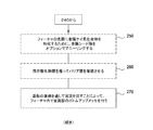
本書に記載の方法及び構造は、クラスタツールなどの集積型処理ツールにそれぞれ連結されているか、又はかかる処理ツールの一部である、個別のチャンバ内で実施されうる。集積型のツールの例は、CENTURA(R)及びENDURA(R)集積型ツール(両方ともカリフォルニア州Santa ClaraのApplied Materials, inc.から入手可能)を含む。一実施形態では、クラスタツールは、周期的層堆積、化学気相堆積(CVD)、物理的気相堆積(PVD)、原子層堆積(ALD)、エッチング、予洗浄、脱ガス、アニーリング、配向付け、及びその他の基板処理といった、いくつかの処理工程を実施するよう構成されている、処理チャンバを有しうる。 The methods and structures described herein may be carried out in individual chambers, each linked to or part of an integrated processing tool such as a cluster tool. Examples of integrated tools include CENTURA (R) and ENDURA (R) integrated tools, both available from Applied Materials, Inc., Santa Clara, CA. In one embodiment, the cluster tool is a periodic layer deposition, chemical vapor deposition (CVD), physical vapor deposition (PVD), atomic layer deposition (ALD), etching, pre-cleaning, degassing, annealing, orientation. , And other substrate processing, which may have a processing chamber configured to perform several processing steps.
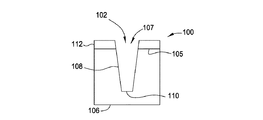
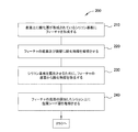
図1Aから図1Hは、処理シーケンス200(図2)の様々な処理工程が基板100に実施される際の、フィーチャ102の概略断面図を示している。工程210において、図1Aに示しているように、基板100にフィーチャ102が形成される。図1Aは、フィールド領域105と、裏側106と、基板100の表面に形成されたフィーチャ102とを有する、基板100の断面図を示している。フィーチャは開口107を有する。フィーチャ102は、少なくとも1つの側壁108と、底面110とによって画定される。一部の実施形態では、底面110は、露出したシリコンの、又はシリコンを含有する表面(単結晶シリコン表面など)である。一部の実施形態では、底面110は、露出したゲルマニウムの、又はゲルマニウムを含有する表面である。一部の実施形態では、底面110は、基板100の露出した表面によって画定される。
1A-1H show schematic cross-sectional views of
フィーチャ102は、少なくとも約5:1以上(例えば、6:1以上、7:1以上、8:1以上、9:1以上、10:1以上、11:1以上、12:1以上、16:1以上、又は約10:1〜約20:1、又は、約30:1〜約50:1の範囲内、又は、約70:1〜約100:1の範囲内)の高さ対幅の高アスペクト比(ベア孔の高さを孔の幅で割った比率)を有する、フィーチャを含みうる。例示的なフィーチャ定義は、半導体デバイス、ソーラーデバイス、又は高比率コンタクトプラグなどのその他の電子デバイスで利用される、ビア、トレンチ、間隙、ライン、コンタクト孔、貫通孔、又はその他のフィーチャ定義を含む。フィーチャ102は、コンタクト孔、ビア、又はトレンチなどの開孔を含みうる。開孔がビアである一部の実施形態では、このビアは、高アスペクト比(例えば、AR〜20−50)を有する。
フィーチャ102は、反応性イオンエッチング技法、又は他の異方的エッチング技法を使用して形成されうる。一実施形態では、フィーチャ102を形成するために、エッチングガスのプラズマ又はイオンビームが基板100へと導かれうる。エッチングガスは、SF6、C3F8CF4、BF3、BI3、N2、Ar、PH3、AsH3、B2H6、H2、Xe、Kr、Ne、He、SiH4、SiF4、GeH4、GeF4、CH4、AsF5、PF3、PF5、又はこれらの組み合わせを含みうる。一実施形態では、フィーチャ102を形成するために、スパッタエッチングが基板100へと方向付けられうる。スパッタエッチングは、アルゴンプラズマを用いて実施されうる。一実施形態では、フィーチャ102は、8kVを上回る電圧バイアスを有するプラズマ注入ツールを使用して形成される。
Feature 102 can be formed using reactive ion etching techniques or other anisotropic etching techniques. In one embodiment, a plasma or ion beam of etching gas may be directed to the
基板100は、例えばシリコン、ゲルマニウム、又はシリコンゲルマニウムなどの、半導体材料を含みうる。フィーチャ102は、従来型のリソグラフィ技法及びエッチング技法を使用して、基板100に形成されうる。一部の実施形態では、フィーチャ102は、ボッシュプロセスなどの、パルスエッチング又は時間多重エッチングのプロセスを使用して形成されうる。
The
一部の実施形態では、図1Aに示すフィーチャ102が形成される前に、フィールド領域105に酸化物層112が形成されうる。酸化物層112は、約500Å〜約1,000Åの範囲内の厚さを有する、酸化物薄層でありうる。酸化物層112は、酸化物を含有するシリコン層(SiO2、SiOなど)でありうる。酸化物層112は、基板100を洗浄プロセスに暴露することによって、フィールド領域105に形成されうる。一部の実施形態では、このオプションの洗浄プロセスは、基板100を標準洗浄−1(SC−1)の化学作用に(例えば、典型的には10分間、摂氏75度又は80度で、NH4OH(水酸化アンモニウム)+H2O2(過酸化水素)+H2O(水)の1:1:5溶液に)暴露することを含みうる。このオプションの予洗浄プロセスは、フッ化水素酸を含有する溶液に暴露することと、標準洗浄2(SC−2)の化学作用に(例えば、摂氏75度又は80度で、HCl+H2O2+H2Oの1:1:6溶液に)暴露することの少なくとも一方を、更に含みうる。一部の実施形態では、化学気相堆積(CVD)などの堆積技法を使用して、フィールド領域105に酸化物層112が形成されうる。
In some embodiments, the
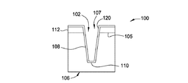
工程220において、図1Bに示しているように、フィーチャ102の酸化物層112、底面110、及び少なくとも1つの側壁108の上に、酸化物層120が形成される。酸化物層120は共形酸化物層でありうる。酸化物層120は、底面110上よりも、少なくとも1つの側壁108上で厚くなりうる。酸化物層120は、約100Å〜約3,000Åの範囲内(例えば、約500Å〜約1,000Å、1,000Å〜約2,000Å、2,000Å〜約3,000Å、2,500Å〜約3,000Å)の厚さを有しうる。一実施形態では、酸化物層120の少なくとも1つの側壁108上の部分は、約2,000Å〜約3,000Åであり、酸化物層120の底面110上の部分は、約500Å〜約1,200Åである。
In
酸化物層120は、酸化物を含有するシリコン層(SiO2、SiOなど)でありうる。酸化物層120は酸化ケイ素又は二酸化ケイ素を含有する層でありうる。酸化ケイ素層又は二酸化ケイ素層は、絶縁層としての役割を果たしうる。酸化ケイ素層又は二酸化ケイ素層は、CVDプロセスを使用して堆積されうる。二酸化ケイ素は、オルトケイ酸テトラエチル(TEOS)に由来するものでありうる。
The
一実施形態では、酸化物層120は、低温CVDプロセス(例えば、温度が摂氏約250〜約300度の範囲内)を使用して堆積される。一実施形態では、酸化物層120は、低バイアスを伴うPVDによって堆積されうる。
In one embodiment, the
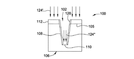
工程230において、図1Cに示しているように、基板100を露出させるために、フィーチャ102の底面110から酸化物層120の一部分が除去される。工程230においては、酸化物層112を露出させるために、フィールド領域105からも酸化物層120の一部分が除去されうる。酸化物層120は、反応性イオンエッチングプロセスやスパッタリングエッチングプロセスなどのエッチングプロセスを使用して、底面110及びフィールド領域105から除去されうる。一部の実施形態では、フィーチャ102の底面110から酸化物層120を除去し、基板100のシリコン材料を露出させるために、酸化物層120の露出した表面が、方向性にエッチングされうる。基板100のフィールド領域105の酸化物層112は、方向性エッチングプロセスにおいて薄化されうるか、又は完全に除去されうる。
In
矢印124’は、処理中に基板の基板表面付近に電界が生成されることによる、ガスイオンの移動の方向を表わしており、この移動により、方向性エッチングプロセスにおいて、アルゴンガスが酸化物層120の上部(平面)表面に衝突する。矢印124”も同じく、フィーチャ102の底面110におけるガスイオンの移動の方向を示している。少なくとも1つの側壁108に沿った酸化物層120は、薄化されうるが、実質的には、エッチングプロセスによる影響を受けない。そのため、少なくとも1つの側壁108を覆って堆積された酸化物層120は、エッチングプロセスが完遂した後にもそのまま残る。少なくとも1つの側壁108上の酸化物層120は、工程230において薄化されうるが、除去されることはない。薄化した残存酸化物層120は導電経路を提供しうるが、薄化した酸化物層120の抵抗は、典型的には非常に高く、その結果として、フィールド領域及び/又は少なくとも1つの側壁に多量のメッキが付くことはなく、ゆえに、ボトムアップ充填が提供される。少なくとも1つの側壁108及びフィールド領域105に沿った酸化物層120により、少なくとも1つの側壁108及びフィールド領域105の銅メッキ又はニッケルメッキが防止される。金属シード層130が形成されるフィーチャ102の底部110には、メッキが行われる。
The arrow 124'indicates the direction of movement of the gas ion due to the generation of an electric field near the substrate surface of the substrate during the process, and this movement causes the argon gas to be transferred to the
エッチングプロセスがスパッタエッチングプロセスである実施形態では、このプロセスは、高バイアスを伴うアルゴンベースのスパッタエッチングプロセスであって、方向性であり、かつ、主に、フィールド領域105から、及び底面110から、酸化物をエッチングする、スパッタエッチングプロセスでありうる。一部の実施形態では、エッチングプロセスの後に底面110に残存酸化物があれば、それは湿式エッチングプロセスによって除去されうる。湿式エッチングプロセスは、80%の酢酸液中の2%のH2O2+3%のフッ化水素酸(15%の脱イオン水)を含む、湿式エッチング溶液を使用して実施されうる。
In embodiments where the etching process is a sputter etching process, the process is an argon-based sputter etching process with high bias, directional and primarily from the
工程240において、図1Dに示しているように、フィーチャ102の底面110の露出したシリコン上に、金属シード層130が堆積される。金属シード層130は、物理的気相堆積(PVD)プロセス、化学気相堆積(CVD)プロセス、電気メッキ堆積プロセス、無電解堆積プロセス、又は原子層堆積(ALD)プロセスを使用して、底面110に堆積されうる。一部の実施形態では、金属シード層130の堆積プロセスは、後述するバリア層の堆積プロセスと同じ堆積チャンバ内で行われうる。一部の実施形態では、金属シード層130は、銅(Cu)の層、ルテニウム(Ru)の層、パラジウム(Pd)の層、ニッケル(Ni)の層、コバルト(Co)の層、又は、これらの元素のうちの一又は複数を含有する合金の層でありうる。一部の実施形態では、金属シード層130は、厚さが約10nm〜約250nmの範囲内である。一部の実施形態では、金属シード層130は、厚さが約100nm〜約200nmの範囲内である。
In
金属シード層130がニッケル層である一部の実施形態では、このニッケル層は、無電解メッキプロセスを使用して堆積されうる。シリコン表面を調製することは、より良好な接着を引き起こすと考えられている化学酸化物を再成長させるための、フッ化水素酸エッチングとSC−1浸漬の少なくとも一方を含みうる。無電解ニッケルメッキ液は、ニッケル源(NiSO4など)と、還元剤(NH4OHなど)と、脱イオン水とを含みうる。還元剤は、無電解ニッケルメッキ液を8を上回るpHに維持するのに役立つ。フィーチャ102の底部110に露出したシリコンが、還元剤として作用する。無電解メッキ液は、約5〜約6のpHを有しうる。無電解ニッケル堆積プロセスは、オプションで固定撹拌又は超音波処理などの撹拌を伴って、摂氏95度以上の温度で実施されうる。
In some embodiments where the
一実施形態では、無電解ニッケルメッキプロセスは、ニッケル置換プロセスである。一実施形態では、無電解ニッケルメッキ液は、100mlの水に0.5MのNiSO4を添加すること、及び、この混合物を摂氏90度を上回るまで加熱することを含む。次いで、30%のNH4OH200mlが、混合物に添加される。混合物の温度は摂氏70度に維持される。基板100はおよそ20分間このメッキ液に浸漬された後、脱イオン水によるすすぎ、N2による乾燥が続く。
In one embodiment, the electroless nickel plating process is a nickel substitution process. In one embodiment, the electroless nickel plating solution comprises adding 0.5 M NiSO 4 to 100 ml of water and heating the mixture to above 90 degrees Celsius. Then 200 ml of 30% NH 4 OH is added to the mixture. The temperature of the mixture is maintained at 70 degrees Celsius.
工程250において、オプションで、フィーチャ102の底面110に金属ケイ素化合物層(図示せず)を形成するために、金属シード層130がアニーリングされうる。金属ケイ素化合物層は、金属シード層130の少なくとも一部分と、シリコンを含有する基板100の少なくとも一部分とを含む。例示的なアニーリングプロセスは、熱アニーリングプロセス(RTPなど)、レーザアニーリングプロセス(ミリ秒アニーリングプロセス、ナノ秒アニーリングプロセス、及びマイクロ秒アニーリングプロセスなど)、並びにフラッシュランプアニーリングプロセスを含む。金属ケイ素化合物層は、摂氏約400度から摂氏約1,200度未満までの範囲内の温度でアニーリングすることによって、形成されうる。金属ケイ素化合物層は、摂氏約700度から摂氏約1,000度未満までの範囲内の温度でアニーリングすることによって、形成されることもある。
In
工程260において、オプションで、基板100内への銅拡散を防止するために、図1Gに示しているように、フィーチャ102内の残存酸化物層120上にバリア層140が形成されうる。バリア層140は、共形層であっても、非共形層であってもよい。バリア層140は、原子層堆積(ALD)、化学気相堆積(CVD)、物理的気相堆積(PVD)、又はこれらの組み合わせを含む好適な堆積プロセスを使用して、形成されうる。共形バリア層は、ALDプロセス又はCVDプロセスによって形成されうる。非共形バリア層はPVDプロセスによって形成されうる。一実施形態では、バリア層140は、低バイアスを伴うPVDプロセスによって堆積されうる。一実施形態では、バリア層140は、クラスタツールの1つのチャンバによって堆積されうる。一実施形態では、基板100は、カリフォルニア州Santa ClaraにあるApplied Materials Inc.から入手可能なULTIMA HDP−CVDTM、Centura iSprintTM、又はEndura iLBTMシステムといった、プラズマALD(PE−ALD)チャンバ、プラズマCVD(PE−CVD)チャンバ、又は高密度プラズマCVD(HDP−CVD)チャンバの中に載置されうる。
In
一実施形態では、バリア層140は、物理的気相堆積(PVD)プロセス、化学気相堆積(CVD)プロセス、又は原子層堆積(ALD)プロセスを使用して形成されうる。バリア層140は、ルテニウム(Ru)、チタン(Ti)、窒化チタン(TiN)、タングステン(W)、窒化タングステン(WN)、窒化タングステンシリコン(WSiN)、タンタル(Ta)、窒化タンタル(TaN)、又はこれらの物質を含有するその他の合金を含有する、単一堆積層であっても多重堆積層であってもよい。一部の実施形態では、単一堆積層又は多重堆積層の積層体は、酸化物層を含みうる。一部の実施形態では、酸化物層は酸化物層120でありうる。酸化物層は酸化ケイ素又は二酸化ケイ素を含有する層でありうる。酸化ケイ素層又は二酸化ケイ素層は、絶縁層としての役割を果たしうる。酸化ケイ素層又は二酸化ケイ素層は、CVDプロセスを使用して堆積されうる。一実施形態では、多重堆積層の積層体は、二酸化ケイ素を含有する第1の層と、TiNを含有する第2の層とを有しうる。二酸化ケイ素は、オルトケイ酸テトラエチル(TEOS)に由来するものでありうる。一部の実施形態では、バリア層140は、約500Å〜約2,000Å(例えば、約1,000Å〜約1,500Å、約1,000Å〜約2,000Å)の厚さでありうる。
In one embodiment, the
酸化物層112が存在する一部の実施形態では、バリア層140は、酸化物層112を覆って堆積される。酸化物層112が存在しない一部の実施形態では、バリア層140は、フィールド領域105上に直接堆積される。
In some embodiments where the
工程270において、図1F及び図1Hに示しているように、基板100の裏側106を通して電流を流すことによる電気めっきプロセスによって、金属層150によるフィーチャ102のボトムアップ充填が行われる。一部の実施形態では、フィーチャ102は、好ましくは、フィーチャ102の底部の金属シード層130から、層がフィールド領域105とほぼ同じ高さになるまで充填される(例えばボトムアップ充填)。一部の実施形態では、金属層150は、銅(Cu)の層、コバルト(Co)の層、ニッケル(Ni)の層、銀(Ag)の層、又は、これらの元素のうちの一又は複数を含有する合金の層でありうる。一部の実施形態では、フィーチャ102は、フィーチャ102を充填するために2つ以上の層が連続して堆積される多重層充填プロセスを使用して、充填される。例示的なボトムアップ充填型電気めっきプロセスについては、図3及び図4を参照して後述する。通常、金属層150は、一又は複数の金属を含有する層の堆積を可能にする一又は複数の金属イオン源を含有する、電気めっき堆積液を使用して堆積されうる。一実施形態では、金属イオンのうちの1つは銅イオンであり、それ以外の金属イオン(複数可)は、アルミニウム(Al)、インジウム(In)、モリブデン(Mo)、タングステン(W)、マンガン(Mn)、コバルト(Co)、スズ(Sn)、ニッケル(Ni)、マグネシウム(Mg)、レニウム(Rh)、ベリリウム(Be)、リン(P)、ホウ素(B)、ガリウム(Ga)、又はルテニウム(Ru)からなる群から選択された金属である。一部の実施形態では、約0.5Amp〜2Ampの電流が使用される。一部の実施形態では、堆積バイアスは概して、約0.0005A/cm2〜約0.01A/cm2以下の電流密度を有する。
In
処理シーケンス200の一部の実施形態では、酸化物層112は、電気化学プロセス又は化学機械研磨プロセス(CMP)などの材料除去プロセスを使用することによって、フィールド領域105から除去されうる。一部の実施形態では、酸化物層120は工程230のプロセスにおいて、フィールド領域105から除去されうる。一部の実施形態では、このプロセス工程は、金属層150の堆積を実施した後にオーバーメッキの残余物があればそれを除去するプロセスを含む。基板100は、メッキ液及び/又は湿式接触液があればそれを除去するための、洗浄プロセスにも暴露されうる。洗浄プロセスは、スピン、すすぎ、及び乾燥のうちの少なくとも1つを含みうる。
In some embodiments of the
図3は、本書に記載の堆積プロセスを実施するために使用されうるメッキセル300の概略断面図を示している。図4は、本書に記載の堆積プロセスを実施するために使用されうるメッキセル300の、別の概略断面図を示している。図3のメッキセル300と図4のメッキセル300とは、使用される湿式接触液以外は同一である。図3及び図4に示す湿式接触液は例示的なものであることも、理解すべきである。メッキセル300は接触液区画310とメッキ液区画320とを備え、基板100がこれらの区画の間に位置付けられている。メッキセル300は、図3では、垂直配向を有する(すなわち、基板が垂直配向を有する)ものとして描かれているが、メッキセル300が、湿式接触液区画310がメッキ液区画320の下に位置付けられる水平配向を有しうることも、理解すべきである。
FIG. 3 shows a schematic cross-sectional view of the plating
可溶性アノード330が、メッキ液区画320内に位置付けられる。可溶性アノード330は、典型的には、基板100にメッキされる材料を含む。例えば、基板100に銅がメッキされる一部の実施形態では、可溶性アノード330は銅を含み、メッキ液区画320内のメッキ液に銅イオンを供給する。
The
不溶性電極340が、湿式接触液区画内に位置付けられる。不溶性電極340は、典型的には、湿式接触液区画内のプロセス化学作用に対して不活性な材料を含む。一部の実施形態では、不溶性電極340はホウ素でドープされた炭素(BDC)を含む。
The
メッキセル300は、メッキセル300の様々な構成要素に電力を供給するための電源360に連結されうる。電源360は、RF電源又は直流電源でありうる。電源360はコントローラ370に連結されうる。コントローラ370は、メッキセル300の動作を制御するために、メッキセル300に連結されうる。コントローラ370は、一又は複数のマイクロプロセッサ、マイクロコンピュータ、マイクロコントローラ、専用のハードウェア又は論理、及びこれらの組み合わせを含みうる。
The plating
メッキ液区画320は、予め混合されたメッキ液、又はメッキ液を形成する前駆体をメッキ液区画320に供給するための、第1流体供給源364に連結されうる。湿式接触液区画310は、湿式接触液、及び追加の添加物があればそれを湿式接触液区画310に供給するための、第2流体供給源366に連結されうる。
The
一部の実施形態では、湿式接触液は、基板100の裏側106に電流を届けることが可能な導電液を含む。一実施形態では、湿式接触液は電解質を含む。一実施形態では、湿式接触液は導電酸を含む。導電酸は、基板100の裏側106からシリコンを除去し、かつ、ウエハと電極との間に電流の流れを提供すると考えられている。導電酸の一例は、フッ化水素酸である。フッ化水素酸は、約10%(w/w)〜約49%(w/w)の水溶液でありうる。湿式接触液は、液の導電性を向上させるために追加の塩を含みうる。例示的な追加の塩はフッ化カリウムを含む。一実施形態では、湿式接触液は、フッ化水素酸溶液、水(49%)、及びフッ化カリウムを含む。
In some embodiments, the wet contact liquid comprises a conductive liquid capable of delivering an electric current to the
一実施形態では、湿式接触液は導電性基剤を含む。一部の実施形態では、導電性基剤は水酸化カリウム(KOH)である。KOHなどの導電性基剤は、典型的には、多孔性シリコンの形成を引き起こすことなく、111結晶配向のシリコンに関して低いエッチング速度(46Å/min)を示す。KOHなどの導電性基剤は、湿式接触を提供するのに十分な〜15A/分で、高温でSiO2をエッチングすることも可能である。実験結果により、KOHベースの湿式接触液を用いる時間に応じてメッキ電流安定性が向上することが、確認された。導電性基剤(KOHなど)を使用することで、導電酸が使用される時に基板100の裏側106に多孔性シリコンが形成されることにより発生しうるメッキ電流の損失が、防止されると考えられている。
In one embodiment, the wet contact liquid comprises a conductive base. In some embodiments, the conductive base is potassium hydroxide (KOH). Conductive bases such as KOH typically exhibit low etching rates (46 Å / min) for 111 crystal oriented silicon without causing the formation of porous silicon. Conductive bases such as KOH are also capable of etching SiO 2 at high temperatures at ~ 15 A / min, which is sufficient to provide wet contact. From the experimental results, it was confirmed that the plating current stability was improved depending on the time when the KOH-based wet contact liquid was used. It is considered that the use of a conductive base (KOH, etc.) prevents the loss of plating current that may occur due to the formation of porous silicon on the
メッキ液
一実施形態では、メッキ液は、金属イオン源と、少なくとも一又は複数の酸性液とを含有する。一部の実施形態では、メッキ液は電気めっき液である。他の実施形態では、メッキ液は無電解メッキ液である。好適な酸性液は、例えば、硫酸、リン酸、ピロリン酸、塩酸、過塩素酸、酢酸、クエン酸、これらの組み合わせ、並びにそれらの酸電解質誘導体(アンモニウム塩及びカリウム塩を含む)などの、無機酸を含む。
Plating Liquid In one embodiment, the plating liquid contains a metal ion source and at least one or more acidic liquids. In some embodiments, the plating solution is an electroplating solution. In other embodiments, the plating solution is an electroless plating solution. Suitable acidic solutions are inorganic, such as, for example, sulfuric acid, phosphoric acid, pyrophosphate, hydrochloric acid, perchloric acid, acetic acid, citric acid, combinations thereof, and their acid electrolyte derivatives (including ammonium and potassium salts). Contains acid.
一部の実施形態では、メッキ液中の金属イオン源は銅イオン源である。有用な銅源は、硫酸銅(CuSO4)、硫化銅(I)(Cu2S)、硫化銅(II)(CuS)、塩化銅(I)(CuCl)、塩化銅(II)(CuCl2)、酢酸銅(II)(Cu(CO2CH3)2)、ピロリン酸銅(Cu2P2O7)、ホウフッ化銅(Cu(BF4)2)、酢酸銅((CH3CO2)2Cu)、銅アセチルアセトナート((C5H7O2)2Cu)、リン酸銅、硝酸銅、炭酸銅、スルファミン酸銅、スルホン酸銅、ピロリン酸銅、シアン化銅、これらの誘導体、これらの水和物、又はこれらの組み合わせを含む。一部の銅源は、CuSO45H2O、CuCl22H2O、及び(CH3CO2)2CuH2Oなどの水和誘導体として、一般的に入手可能である。電解質の組成は、アルカリ性銅メッキ槽(例えば、シアン化物、グリセリン、アンモニアなど)に基づくものであることも可能である。一実施形態では、電解質中の銅イオンの濃度は、約0.1M〜約1.1Mの範囲にわたりうる。一実施形態では、電解質中の銅イオンの濃度は、約0.4M〜約0.9Mの範囲にわたりうる。 In some embodiments, the metal ion source in the plating solution is a copper ion source. Useful copper sources, copper sulfate (CuSO 4), copper sulfide (I) (Cu 2 S) , copper sulfide (II) (CuS), copper chloride (I) (CuCl), copper chloride (II) (CuCl 2 ), Copper acetate (II) (Cu (CO 2 CH 3 ) 2 ), Copper pyrophosphate (Cu 2 P 2 O 7 ), Copper borofluoride (Cu (BF 4 ) 2 ), Copper acetate ((CH 3 CO 2)) ) 2 Cu), copper acetylacetonate ((C 5 H 7 O 2 ) 2 Cu), copper phosphate, copper nitrate, copper carbonate, sulfamate, copper sulfonate, copper pyrophosphate, copper cyanide, these Includes derivatives, hydrates thereof, or combinations thereof. Part of the copper source, CuSO 4 5H 2 O, as hydrated derivatives of such CuCl 2 2H 2 O, and (CH 3 CO 2) 2 CuH 2 O, which is commonly available. The composition of the electrolyte can also be based on an alkaline copper plating tank (eg cyanide, glycerin, ammonia, etc.). In one embodiment, the concentration of copper ions in the electrolyte can range from about 0.1M to about 1.1M. In one embodiment, the concentration of copper ions in the electrolyte can range from about 0.4M to about 0.9M.
一実施形態では、メッキ液は無添加メッキ液である。一実施形態では、無添加メッキ液は硫酸銅のみを含有する。 In one embodiment, the plating solution is an additive-free plating solution. In one embodiment, the additive-free plating solution contains only copper sulfate.
オプションで、メッキ液は、一又は複数の添加化合物を含みうる。一部の実施形態では、メッキ液は酸化剤を含有する。本書において、酸化剤は、金属層を対応する酸化物に(例えば、銅を酸化銅に)酸化させるために使用されうる。好適な酸化剤の例は、ペルオキシ化合物、例えば、過酸化水素尿素、過炭酸塩、及び有機過酸化物(アルキル過酸化物、環状過酸化物又はアリール過酸化物、過酸化ベンゾイル、過酢酸、ジ‐t‐ブチル過酸化物などを含む)を含む過酸化水素及びその付加体などのヒドロキシラジカルを通じて解離しうる化合物を、含む。ペルオキシ二硫酸アンモニウム、ペルオキシ二硫酸カリウム、過硫酸アンモニウム、及び過硫酸カリウムなどを含む、硫酸塩及び硫酸誘導体(モノ過硫酸塩及び二過硫酸塩など)も使用されうる。過炭酸ナトリウム及び過酸化ナトリウムなどのペルオキシ化合物の塩も、使用されうる。一部の実施形態では、約0.001%〜約90%(質量パーセント又は重量パーセント)の範囲にわたる量の酸化剤が、メッキ液中に存在しうる。別の実施形態では、約0.01%〜約20%(質量パーセント又は重量パーセント)の範囲にわたる量の酸化剤が、メッキ液中に存在しうる。更に別の実施形態では、約0.1%〜約15%(質量パーセント又は重量パーセント)の範囲にわたる量の酸化剤が、メッキ液中に存在することもある。 Optionally, the plating solution may contain one or more additive compounds. In some embodiments, the plating solution contains an oxidant. In this document, an oxidizing agent can be used to oxidize a metal layer to a corresponding oxide (eg, copper to copper oxide). Examples of suitable oxidizing agents include peroxy compounds such as hydrogen peroxide urea, percarbonates, and organic peroxides (alkyl peroxides, cyclic peroxides or aryl peroxides, benzoyl peroxide, peracetic acid, etc. Contains compounds that can be dissociated through hydroxy radicals such as hydrogen peroxide and its adducts (including di-t-butyl peroxide and the like). Sulfates and sulfate derivatives (such as monosulfate and dipersulfate), including ammonium peroxydisulfate, potassium peroxydisulfate, ammonium persulfate, and potassium persulfate, may also be used. Salts of peroxy compounds such as sodium percarbonate and sodium peroxide can also be used. In some embodiments, an amount of oxidant ranging from about 0.001% to about 90% (mass percent or weight percent) may be present in the plating solution. In another embodiment, an amount of oxidant ranging from about 0.01% to about 20% (mass percent or weight percent) may be present in the plating solution. In yet another embodiment, an amount of oxidant ranging from about 0.1% to about 15% (mass percent or weight percent) may be present in the plating solution.
一部の実施形態では、望ましいpHを有する安価な電解質を形成して、エネルギーデバイスを形成する所有コストを削減するために、水酸化カリウム(KOH)や水酸化ナトリウム(NaOH)などの低コストのpH調整剤を添加することが望ましい。一部の実施形態では、pHを調整するためにテトラメチルアンモニウム水酸化物(TMAH)を使用することが望ましい。 In some embodiments, low cost, such as potassium hydroxide (KOH) or sodium hydroxide (NaOH), is used to form an inexpensive electrolyte with the desired pH and reduce the cost of ownership to form the energy device. It is desirable to add a pH adjuster. In some embodiments, it is desirable to use tetramethylammonium hydroxide (TMAH) to adjust the pH.
一部の実施形態では、電気化学的に堆積される成長層若しくはこの層の粒界をプレートアウトするか、又は、かかる層若しくは粒界に組み込まれる、主たる金属イオンを含有する電解槽(例えば銅イオンを含有する槽)に第2の金属イオンを添加することが望ましいこともある。一定割合の第2元素を含有する金属層の形成は、形成された層の内在応力を低減するため、及び/又は、その電気的特性及びエレクトロマイグレーション特性を改善するために、役立ちうる。一実施形態では、電解質溶液中の金属イオン源は、銀、スズ、亜鉛、コバルト、ニッケルのイオン源、及びこれらの組み合わせかを含む群から選択されたイオン源である。一実施形態では、電解質中の銀(Ag)、スズ(Sn)、亜鉛(Zn)、コバルト(Co)、又はニッケル(Ni)のイオン濃度は、約0.1M〜約0.4Mの範囲にわたりうる。 In some embodiments, an electrochemically deposited growth layer or grain boundaries of this layer are plated out or incorporated into such layers or grain boundaries, an electrolytic cell containing a major metal ion (eg, copper). It may be desirable to add a second metal ion to the ion-containing tank). The formation of a metal layer containing a certain percentage of the second element can be useful for reducing the intrinsic stress of the formed layer and / or for improving its electrical and electromigration properties. In one embodiment, the metal ion source in the electrolyte solution is an ion source selected from the group comprising silver, tin, zinc, cobalt, nickel ion sources, and combinations thereof. In one embodiment, the ion concentration of silver (Ag), tin (Sn), zinc (Zn), cobalt (Co), or nickel (Ni) in the electrolyte ranges from about 0.1M to about 0.4M. sell.
好適なニッケル源の例は、硫酸ニッケル、塩化ニッケル、酢酸ニッケル、リン酸ニッケル、これらの誘導体、これらの水和物、又はこれらの組み合わせを含む。 Examples of suitable nickel sources include nickel sulfate, nickel chloride, nickel acetate, nickel phosphate, derivatives thereof, hydrates thereof, or combinations thereof.
好適なスズ源の例は、可溶性スズ化合物を含む。可溶性スズ化合物は第二スズ塩又は第一スズ塩でありうる。第二スズ塩又は第一スズ塩は、硫酸塩、アルカンスルホン酸塩、又はアルカノールスルホン酸塩でありうる。例えば、槽可溶性のスズ化合物は、
(RSO3)2Sn
という化学式で表わされる、一又は複数のアルカンスルホン酸第一スズ(stannous alkane sulfonate)であってよく、この式中、Rは、1〜12の炭素原子を含むアルキル基である。アルカンスルホン酸第一スズは、

(RSO 3 ) 2 Sn
It may be one or more stannous alkane sulfone represented by the chemical formula, and in this formula, R is an alkyl group containing 1 to 12 carbon atoms. Stannous alkane sulfonate is
可溶性スズ化合物の例は、メタンスルホン酸、エタンスルホン酸、2−プロパノールンスルホン酸、p‐フェノールスルホン酸及び同類、ホウフッ化スズ(II)、スズ(II)スルホスクシネート(tin(II)sulfosuccinate)、硫酸スズ(II)、酸化スズ(II)、塩化スズ(II)及び同類といった、有機スルホン酸のスズ(II)塩も含みうる。これらの可溶性スズ(II)化合物は、単独でも、2つ以上の種類の組み合わせでも、使用されうる。 Examples of soluble tin compounds are methanesulfonic acid, ethanesulfonic acid, 2-propanolnsulfonic acid, p-phenolsulfonic acid and the like, tin borofluoride (II), tin (II) sulfosuccinate (tin (II)). It may also include tin (II) salts of organic sulfonic acids such as sulphosuccinate), tin (II) sulfate, tin (II) oxide, tin (II) chloride and the like. These soluble tin (II) compounds can be used alone or in combination of two or more types.
好適なコバルト源の例は、硫酸コバルト、硝酸コバルト、塩化コバルト、臭化コバルト、炭酸コバルト、酢酸コバルト、エチレンジアミン四酢酸コバルト、コバルト(II)アセチルアセトネート(cobalt(II)acetyl acetonate)、コバルト(III)アセチルアセトネート(cobalt(III)acetyl acetonate)、グリシンコバルト(III)、ピロリン酸コバルト、及びこれらの組み合わせから選択された、コバルト塩を含みうる。 Examples of suitable cobalt sources are cobalt sulfate, cobalt nitrate, cobalt chloride, cobalt bromide, cobalt carbonate, cobalt acetate, cobalt diamine tetraacetate, cobalt (II) acetylacetonate, cobalt ( III) It may contain a cobalt salt selected from cobalt (III) acetatel acetonate, glycine cobalt (III), cobalt pyrophosphate, and combinations thereof.
メッキ液は、約20ppm〜約600ppmの範囲内の濃度のマンガン又は鉄も含有しうる。別の実施形態では、メッキ液は、約100ppm〜約400ppmの範囲内の濃度のマンガン又は鉄を含有することもある。使用可能な鉄源は、水和物を含む塩化鉄(II)(FeCl2)、塩化鉄(III)(FeCl3)、酸化鉄(II)(FeO)、酸化鉄(II、III)(Fe3O4)、及び酸化鉄(III)(Fe2O3)を含む。使用可能なマンガン源は、酸化マンガン(IV)(MnO2)、硫酸マンガン(II)一水和物(MnSO4・H2O)、塩化マンガン(II)(MnCl2)、塩化マンガン(III)(MnCl3)、フッ化マンガン(MnF4)、及びリン酸マンガン(Mn3(PO4)2)を含む。 The plating solution may also contain manganese or iron at a concentration in the range of about 20 ppm to about 600 ppm. In another embodiment, the plating solution may contain manganese or iron at a concentration in the range of about 100 ppm to about 400 ppm. Available iron sources are iron (II) chloride (FeCl 2 ) containing hydrate, iron (III) chloride (FeCl 3 ), iron (II) oxide (FeO), iron (II, III) oxide (Fe). 3 O 4 ) and iron (III) oxide (Fe 2 O 3 ) are included. Usable manganese sources are manganese oxide (IV) (MnO 2 ), manganese sulfate (II) monohydrate (MnSO 4 · H 2 O), manganese chloride (II) (MnCl 2 ), manganese chloride (III). (MnCl 3 ), manganese fluoride (MnF 4 ), and manganese phosphate (Mn 3 (PO 4 ) 2 ) are included.
一部の実施形態では、メッキ液は、銅源化合物の代わりの自由銅イオン、及び錯化された銅イオンを含有する。 In some embodiments, the plating solution contains free copper ions instead of copper source compounds, and complexed copper ions.
一部の実施形態では、メッキ液は、堆積プロセスにおいて、安定性及び制御を提供すると共に銅イオンを有する錯体を形成するために、少なくとも1つの錯化剤又はキレート剤も含みうる。錯化剤は更に、無電解銅溶液に緩衝特性を提供する。錯化剤は通常、カルボン酸、ジカルボン酸、ポリカルボン酸、アミノ酸、アミン、ジアミン、又はポリアミンなどの、官能基を有する。無電解銅溶液向けの有用な錯化剤の特定の例は、エチレンジアミン四酢酸(EDTA)、エチレンジアミン(EDA)、クエン酸、クエン酸エステル、グリオキシル酸、グリシン、アミノ酸、これらの誘導体、これらの塩、又はこれらの組み合わせを含む。一実施形態では、メッキ液は、約50mM〜約500mMの範囲内の濃度の錯化剤を有しうる。別の実施形態では、メッキ液は、約75mM〜約400mMの範囲内の濃度の錯化剤を有しうる。更に別の実施形態では、メッキ液は、約100mM〜約300mMの範囲内(例えば約200mM)の濃度の錯化剤を有することもある。一実施形態では、EDTA源は、メッキ液中の錯化剤として使用される。一例では、メッキ液は約205mMのEDTA源を含有する。EDTA源は、EDTA、エチレンジアミンテトラアセテート、それらの塩、それらの誘導体、又はそれらの組み合わせを含みうる。 In some embodiments, the plating solution may also include at least one complexing agent or chelating agent to provide stability and control in the deposition process and to form a complex with copper ions. The complexing agent also provides buffering properties for electroless copper solutions. Complexing agents usually have functional groups such as carboxylic acids, dicarboxylic acids, polycarboxylic acids, amino acids, amines, diamines, or polyamines. Specific examples of useful complexing agents for electroless copper solutions include ethylenediaminetetraacetic acid (EDTA), ethylenediamine (EDA), citric acid, citric acid esters, glyoxylic acid, glycine, amino acids, derivatives thereof, salts thereof. , Or a combination thereof. In one embodiment, the plating solution may have a complexing agent with a concentration in the range of about 50 mM to about 500 mM. In another embodiment, the plating solution may have a complexing agent with a concentration in the range of about 75 mM to about 400 mM. In yet another embodiment, the plating solution may have a complexing agent having a concentration in the range of about 100 mM to about 300 mM (eg, about 200 mM). In one embodiment, the EDTA source is used as a complexing agent in the plating solution. In one example, the plating solution contains an EDTA source of about 205 mM. The EDTA source can include EDTA, ethylenediaminetetraacetate, salts thereof, derivatives thereof, or combinations thereof.
ある種の実施形態では、メッキ液は少なくとも1つの還元体を含有する。還元体は、本書に記載しているように、銅材料を形成し堆積させている間に銅イオンの化学還元を引き起こすための、電子を提供する。還元体は、有機還元体(グリオキシル酸やホルムアルデヒドなど)、ヒドラジン、有機ヒドラジン(メチルヒドラジンなど)、次亜リン酸塩源(例えば、次亜リン酸(H3PO2)、次亜リン酸アンモニウム((NH4)4−xHxPO2)、又はこれらの塩)、ボラン源(例えば、ジメチルアミンボラン錯体((CH3)2NHBH3)、DMAB)、トリメチルアミンボラン錯体((CH3)3NBH3)、TMAB)、ボラン−t−ブチルアミン錯体(tBuNH2BH3)、テトラヒドロフランボラン錯体(THFBH3)、ピリジンボラン錯体(C5H5NBH3)、アンモニアボラン錯体(NH3BH3)、ボラン(BH3)、ジボラン(B2H6)、これらの誘導体、これらの錯体、これらの水和物、又はこれらの組み合わせ)を含む。一実施形態では、メッキ液は、約20mM〜約500mMの範囲内の濃度の還元体を有しうる。別の実施形態では、メッキ液は、約100mM〜約400mMの範囲内の濃度の還元体を有しうる。更に別の実施形態では、メッキ液は、約150mM〜約300mMの範囲内(例えば約200mM)の濃度の還元体を有することもある。好ましくは、グリオキシル酸又はグリオキシル酸源などの、有機還元体又は有機物を含有する還元体が、メッキ液中で利用される。グリオキシル酸源は、グリオキシル酸、グリオキシレート、これらの塩、これらの錯体、これらの誘導体、又はこれらの組み合わせを含みうる。一例では、約217mMの濃度のグリオキシル酸一水和物(HCOCO2H・H2O)が、無電解銅溶液中に含有される。 In certain embodiments, the plating solution contains at least one reducer. The reducer provides electrons to cause the chemical reduction of copper ions during the formation and deposition of the copper material, as described herein. The reduced form is an organic reduced form (such as glyoxylic acid or formaldehyde), hydrazine, organic hydrazine (such as methylhydrazine), a hypophosphite source (eg, hypophosphite (H 3 PO 2 ), ammonium hypophosphate). ((NH 4 ) 4-x H x PO 2 ), or salts thereof), borane sources (eg, dimethylamine borane complex ((CH 3 ) 2 NHBH 3 ), DMAB), trimethylamine borane complex ((CH 3 )). 3 NBH 3 ), TMAB), borane-t-butylamine complex (tBuNH 2 BH 3 ), tetrahydrofuran borane complex (THBH 3 ), pyridine borane complex (C 5 H 5 NBH 3 ), ammonia borane complex (NH 3 BH 3 ) , Borane (BH 3 ), diborane (B 2 H 6 ), derivatives thereof, complexes thereof, hydrates thereof, or combinations thereof). In one embodiment, the plating solution may have a reducer at a concentration in the range of about 20 mM to about 500 mM. In another embodiment, the plating solution may have a reducer at a concentration in the range of about 100 mM to about 400 mM. In yet another embodiment, the plating solution may have a reducer at a concentration in the range of about 150 mM to about 300 mM (eg, about 200 mM). Preferably, an organic reduced product or a reduced product containing an organic substance, such as glyoxylic acid or a glyoxylic acid source, is utilized in the plating solution. Glyoxylic acid sources can include glyoxylic acid, glyoxylates, salts thereof, complexes thereof, derivatives thereof, or combinations thereof. In one example, a concentration of about 217 mM glyoxylic acid monohydrate (HCOCO 2 H · H 2 O) is contained in the electroless copper solution.
メッキ液は、例えばレベラー、阻害剤、抑制剤、光沢剤、促進剤、又はそれ以外の当該技術分野において既知の添加物であってよく、かつ、典型的には、メッキされる基板の表面上に吸着する有機材料である、他の添加物を含有しうる。有用な抑制剤は、典型的には、基板表面上に吸着し、吸着エリアにおける銅堆積を減速させる、ポリエチレン、グリコール、又は、酸化ポリプロピレンなどのその他のポリマーといった、ポリエーテルを含む。有用な促進剤は、典型的には、吸着部位で抑制剤と拮抗し、吸着エリアにおける銅堆積を加速させる、ビス−(3−スルホプロピル)ジスルフィドなどの硫化物又は二硫化物を含む。有用な阻害剤は、典型的には、基板上での銅堆積の速度を抑制する、安息香酸ナトリウム及び亜硫酸ナトリウムを含む。メッキ時に、添加物は基板表面において消費されるが、電気めっき液によって継続的に補充される。しかし、様々な添加物の拡散速度が異なることにより、フィーチャの上部と底部とに別々の表面濃度がもたらされ、ひいては、フィーチャ内でのメッキ速度が別様になる。ボトムアップ充填のために、理想的には、メッキ速度は、フィーチャの底部においてより早くなるべきである。ゆえに、フィーチャのボイドフリー充填を実現するために、メッキ液中の適切な組成の添加物が使用されうる。 The plating solution may be, for example, a leveler, an inhibitor, an inhibitor, a brightener, an accelerator, or other additive known in the art, and typically on the surface of the substrate to be plated. It may contain other additives that are organic materials that adsorb to. Useful inhibitors typically include polyethers such as polyethylene, glycol, or other polymers such as polypropylene oxide that adsorb on the surface of the substrate and slow down copper deposition in the adsorption area. Useful accelerators typically include sulfides or disulfides such as bis- (3-sulfopropyl) disulfides that antagonize the inhibitor at the adsorption site and accelerate copper deposition in the adsorption area. Useful inhibitors typically include sodium benzoate and sodium sulfite, which suppress the rate of copper deposition on the substrate. During plating, the additives are consumed on the substrate surface but are continuously replenished by the electroplating solution. However, the different diffusion rates of the various additives result in different surface concentrations at the top and bottom of the feature, which in turn results in different plating rates within the feature. Ideally, for bottom-up filling, the plating rate should be higher at the bottom of the feature. Therefore, additives of appropriate composition in the plating solution can be used to achieve void-free filling of features.
メッキ液は、界面活性剤も有しうる。界面活性剤は、銅を含有する溶液と基板表面との間の表面張力を低減するための、湿潤剤として作用する。一実施形態では、メッキ液は概して、約1,000ppm以下の濃度の界面活性剤を含有する。別の実施形態では、メッキ液は概して、約500ppm以下(例えば、約100ppm〜約300ppmの範囲内)の濃度の界面活性剤を含有する。界面活性剤は、イオン特性又は非イオン特性を有しうる。例示的な界面活性剤は、ポリエチレングリコール(PEG)、ポリプロピレングリコール(PPG)などといった、グリコールエーテルベースの界面活性剤を含む。PEG及びPPGは、有利な特性により、界面活性剤、阻害剤、及び/又は抑制剤として使用されうる。一例では、グリコールエーテルベースの界面活性剤は、The Dow Chemical Companyから入手可能なTRITON(R) 100などの、ポリオキシエチレンユニットを含有しうる。無電解銅溶液中で使用されうる他の界面活性剤は、ドデシル硫酸ナトリウム(SDS)などの硫酸ドデシルを含む。界面活性剤は、単一の化合物であっても、異なる長さの炭化水素鎖を含有する分子を有する化合物の混合体であってもよい。 The plating solution may also have a surfactant. The surfactant acts as a wetting agent to reduce the surface tension between the copper-containing solution and the substrate surface. In one embodiment, the plating solution generally contains a surfactant at a concentration of about 1,000 ppm or less. In another embodiment, the plating solution generally contains a surfactant at a concentration of about 500 ppm or less (eg, in the range of about 100 ppm to about 300 ppm). Surfactants can have ionic or nonionic properties. Exemplary surfactants include glycol ether-based surfactants such as polyethylene glycol (PEG), polypropylene glycol (PPG) and the like. PEG and PPG can be used as surfactants, inhibitors, and / or inhibitors due to their advantageous properties. In one example, glycol ether-based surfactants may contain polyoxyethylene units, such as TRITON (R) 100, available from The Dow Chemical Company. Other surfactants that can be used in electroless copper solutions include dodecyl sulfate, such as sodium dodecyl sulfate (SDS). The surfactant may be a single compound or a mixture of compounds having molecules containing hydrocarbon chains of different lengths.
上述のメッキ液の残部は、水(脱イオン水など)を含む極性溶媒などの溶媒、及び、有機溶媒(アルコールやグリコールなど)でありうる。 The balance of the plating solution described above may be a solvent such as a polar solvent containing water (deionized water or the like) or an organic solvent (alcohol, glycol or the like).
一実施形態では、1Lのメッキ液は、220g/LのCuSO4と、27ml/LのH2SO4と、微量のHClと、脱イオン水である残部とを含む。 In one embodiment, the plating solution 1L includes a CuSO 4 in 220 g / L, and H 2 SO 4 in 27 ml / L, and HCl traces, and balance deionized water.
例
以下の非限定的な例は、本書に記載の実施形態を更に例示するものである。しかし、これらの例は、本書に記載の実施形態の全てを網羅することを意図しておらず、かつ、その範囲を限定することを意図するものでもない。
Examples The following non-limiting examples further illustrate the embodiments described herein. However, these examples are not intended to cover all of the embodiments described herein and are not intended to limit their scope.
例1:
8×8cmのサイズのシリコン試片が、無電解ニッケルメッキ液に暴露された。このニッケルメッキ液は、100mlの水に0.5MのNiSO4を添加すること、及び、この混合物を摂氏90度を上回るまで加熱することによって、形成された。次いで、30%のNH4OH200mlが混合物に添加された。混合物の温度は摂氏70度に維持された。基板100はおよそ20分間この無電解メッキ液に浸漬された後、脱イオン水によるすすぎ、N2による乾燥が続いた。
Example 1:
Silicon shards sized 8 x 8 cm were exposed to electroless nickel plating. The nickel plating solution was formed by adding 0.5 M of NiSO 4 to 100 ml of water and heating the mixture to above 90 degrees Celsius. Then 200 ml of 30% NH 4 OH was added to the mixture. The temperature of the mixture was maintained at 70 degrees Celsius. After the
シリコン試片は、図3のメッキセル300に類似したメッキセル内に位置付けられた。シリコン試片の表側が、220g/LのCuSO4と、27ml/LのH2SO4と、微量のHClと、脱イオン水とである残部とを含む1Lのメッキ液に暴露された。シリコン試片の裏側は、フッ化水素酸溶液、水(49%)、及びフッ化カリウムを含む湿式接触液に暴露された。0.005アンペア/平方センチメートル(A/cm2)の電流密度、及び1.24〜1.3ボルトの電位が、およそ4分間にわたって印加された。シリコン試片上には銅薄層が堆積され、裏側の湿式接触を使用してシリコンに銅がメッキされうることが、成功裏に示された。
The silicon slab was positioned in a plating cell similar to the
要約すると、本開示の実施形態の一部の利点のいくつかは、接触材料がボイド、シーム、及び他の不具合なしに堆積されるように導電性接触材料でフィーチャを充填するための方法を、提供するものである。本書に記載の改良型の方法は、高アスペクト比のフィーチャを充填するのに、特に有利である。本書に記載の実施形態は、Si貫通電極(TSV)の応用において特に有利である。一部の実施形態では、銅メッキ速度を最大化するために、最小限の添加物しか有しない単純な銅包含化学作用を用いて、ボトムアップメッキを行うことにより、不具合のない堆積が実現される。本書に記載の一部の実施形態では、ウエハ裏側の湿式接触を使用する、ボトムアップ式のビアメッキのための方法が、速いメッキ速度での共形銅堆積を実現するために使用される。本書において、「基板(substrate)」とは、その上に層が形成されることも、されないこともある、支持基板でありうる。パターン基板は、ドーピング濃度及びプロファイルが多種多様な絶縁体又は半導体であってよく、例えば、集積回路の製造で使用される種類の半導体基板でありうる。パターン基板の露出した「シリコン(silicon)」とは、主としてSiであるが、少量濃度の、窒素、酸素、水素、炭素などといった他の元素成分も含みうる。パターン基板の露出した「窒化ケイ素(silicon nitride)」とは、主としてSi3N4であるが、少量濃度の、酸素、水素、炭素などといった他の元素成分も含みうる。パターン基板の露出した「酸化ケイ素(silicon oxide)」とは、主としてSiO2であるが、少量濃度の、窒素、水素、炭素などといった他の元素成分も含みうる。 In summary, some of the advantages of some of the embodiments of the present disclosure are methods for filling features with conductive contact material so that the contact material is deposited without voids, seams, and other defects. It is to provide. The improved method described herein is particularly advantageous for filling features with high aspect ratios. The embodiments described herein are particularly advantageous in the application of Through Silicon Vias (TSVs). In some embodiments, bottom-up plating is performed using simple copper-containing chemistry with minimal additives to maximize copper plating rates, resulting in defect-free deposition. To. In some embodiments described herein, a method for bottom-up via plating using wet contact on the back of the wafer is used to achieve conformal copper deposition at high plating rates. In this document, the "substrate" may be a support substrate on which layers may or may not be formed. The pattern substrate may be an insulator or semiconductor having a wide variety of doping concentrations and profiles, and may be, for example, the type of semiconductor substrate used in the manufacture of integrated circuits. The exposed "silicon" of the pattern substrate is mainly Si, but may also contain small concentrations of other elemental components such as nitrogen, oxygen, hydrogen, carbon and the like. The exposed "silicon nitride" of the pattern substrate is mainly Si 3 N 4 , but may also contain small concentrations of other elemental components such as oxygen, hydrogen, carbon and the like. The exposed "silicon oxide" of the pattern substrate is mainly SiO 2 , but may also contain a small concentration of other elemental components such as nitrogen, hydrogen, carbon and the like.
いくつかの実施形態を開示してきたが、開示されている実施形態の本質から逸脱しなければ、様々な変形例、代替構造、及び同等物が使用されうることが、当業者には認識されよう。あるいは、本発明を不必要に分かりにくくすることを避けるために、いくつかの周知のプロセス及び要素については説明しなかった。したがって、上記の説明は、本開示の範囲を限定するものと解釈すべきではない。 Although some embodiments have been disclosed, those skilled in the art will recognize that various variations, alternative structures, and equivalents may be used without departing from the essence of the disclosed embodiments. .. Alternatively, some well-known processes and elements have not been described in order to avoid unnecessarily obscuring the invention. Therefore, the above description should not be construed as limiting the scope of this disclosure.
本開示の要素、又はそれらの例示的な態様又は実施形態(複数可)を紹介する場合の、冠詞の「1つの(a、an)」及び「前記(the、said)」は、一又は複数の要素が存在していることを意味するためのものである。 When introducing the elements of the present disclosure, or exemplary embodiments or embodiments thereof, the articles "one (a, an)" and "the above (the, side)" may be one or more. It is meant to mean that the element of is present.
「備える(comprising)」、「含む(including)」、及び「有する(having)」という語は、包括的であることが意図されており、列挙された要素以外にも追加の要素がありうることを意味する。 The terms "comprising," "inclusion," and "having" are intended to be inclusive, and there may be additional elements beyond those listed. Means.
量、比率、割合、及びその他の測定値は全て、別様の記載がない限り、重量によるものである。パーセンテージは全て、別様の記載がない限り、本開示の慣例にしたがった、全体組成に基づく重量パーセントに言及している。 All quantities, ratios, proportions, and other measurements are by weight unless otherwise stated. All percentages refer to weight percent based on overall composition, as is customary in the present disclosure, unless otherwise stated.
以上の記述は本開示の実施形態を対象としているが、本開示の基本的な範囲から逸脱しなければ、本開示の他の実施形態及び更なる実施形態が考案されてよく、本開示の範囲は、下記の特許請求の範囲によって決まる。 Although the above description is intended for the embodiments of the present disclosure, other embodiments and further embodiments of the present disclosure may be devised as long as they do not deviate from the basic scope of the present disclosure. Depends on the scope of claims below.
Claims (15)
シリコン基板に形成されたフィーチャの少なくとも1つの側壁と底面とを覆って、共形酸化物層を堆積させることであって、前記シリコン基板が、
前記フィーチャを取り囲むフィールド領域と、
裏側とを備え、前記フィーチャは前記フィールド領域から前記裏側に向かって延在する、共形酸化物層を堆積させることと、
前記シリコン基板の一部分を露出させるために、前記フィーチャの前記底面から前記共形酸化物層の一部分を選択的に除去することと、
前記フィーチャの底面の前記シリコン基板が露出した前記一部分に、金属シード層を堆積させることと、
前記シリコン基板が露出した前記一部分に前記金属シード層を堆積させた後に、前記共形酸化物層上に共形バリア層を形成することと、
前記金属シード層上に金属層を形成するために、前記シリコン基板の前記裏側を通して電流を流すことによって前記シリコン基板を電気メッキプロセスに暴露することとを含む、方法。 A method for depositing material on a substrate,
A conformal oxide layer is deposited over at least one side wall and bottom surface of a feature formed on a silicon substrate.
The field area surrounding the feature and
By depositing a conformal oxide layer with a backside, the feature extending from the field area towards the backside.
To selectively remove a portion of the conformal oxide layer from the bottom surface of the feature in order to expose a portion of the silicon substrate.
To deposit a metal seed layer on the exposed part of the silicon substrate on the bottom surface of the feature.
After depositing the metal seed layer on the part where the silicon substrate is exposed, forming a conformal barrier layer on the conformal oxide layer, and
A method comprising exposing the silicon substrate to an electroplating process by passing an electric current through the backside of the silicon substrate to form a metal layer on the metal seed layer.
シリコン基板に形成されたフィーチャの少なくとも1つの側壁と底面とを覆って、酸化物層を堆積させることであって、前記シリコン基板が、
前記フィーチャを取り囲む、表面上に前記酸化物層が配置されているフィールド領域と、
裏側とを備え、前記フィーチャは前記フィールド領域から前記裏側に向かって延在する、酸化物層を堆積させることと、
前記シリコン基板の一部分を露出させるために、前記フィーチャの前記底面から前記酸化物層の一部分を選択的に除去することであって、前記酸化物層の少なくとも一部分が、前記少なくとも1つの側壁に残る、選択的に除去することと、
前記フィーチャの底面の前記シリコン基板が露出した前記一部分に、金属シード層を堆積させることと、
前記酸化物層の前記少なくとも1つの側壁に残っている前記一部分の上に、バリア層を形成することと、
前記金属シード層上に金属層を形成するために、前記シリコン基板の前記裏側を通して電流を流すことによって前記シリコン基板を電気メッキプロセスに暴露することとを含む、方法。 A method for depositing material on a substrate,
An oxide layer is deposited over at least one side wall and a bottom surface of a feature formed on a silicon substrate.
A field region in which the oxide layer is arranged on the surface surrounding the feature, and
With a backside, the feature deposits an oxide layer extending from the field area towards the backside.
To selectively remove a portion of the oxide layer from the bottom surface of the feature in order to expose a portion of the silicon substrate, at least a portion of the oxide layer remains on the at least one side wall. , Selectively remove and
To deposit a metal seed layer on the exposed part of the silicon substrate on the bottom surface of the feature.
To form a barrier layer on the portion of the oxide layer remaining on the at least one side wall.
A method comprising exposing the silicon substrate to an electroplating process by passing an electric current through the backside of the silicon substrate to form a metal layer on the metal seed layer.
Applications Claiming Priority (3)
| Application Number | Priority Date | Filing Date | Title |
|---|---|---|---|
| US201662281470P | 2016-01-21 | 2016-01-21 | |
| US62/281,470 | 2016-01-21 | ||
| PCT/US2016/067571 WO2017127197A1 (en) | 2016-01-21 | 2016-12-19 | Process and chemistry of plating of through silicon vias |
Publications (3)
| Publication Number | Publication Date |
|---|---|
| JP2019504503A JP2019504503A (en) | 2019-02-14 |
| JP2019504503A5 JP2019504503A5 (en) | 2020-02-06 |
| JP6903061B2 true JP6903061B2 (en) | 2021-07-14 |
Family
ID=59359138
Family Applications (1)
| Application Number | Title | Priority Date | Filing Date |
|---|---|---|---|
| JP2018537774A Active JP6903061B2 (en) | 2016-01-21 | 2016-12-19 | Plating process and chemistry of through silicon vias |
Country Status (6)
| Country | Link |
|---|---|
| US (1) | US9935004B2 (en) |
| JP (1) | JP6903061B2 (en) |
| KR (1) | KR20180097179A (en) |
| CN (1) | CN108474129B (en) |
| TW (1) | TWI718227B (en) |
| WO (1) | WO2017127197A1 (en) |
Families Citing this family (25)
| Publication number | Priority date | Publication date | Assignee | Title |
|---|---|---|---|---|
| JP6574207B2 (en) | 2014-05-05 | 2019-09-11 | スリーディー グラス ソリューションズ,インク3D Glass Solutions,Inc | 2D and 3D inductors, antennas, and transformers for manufacturing photoactive substrates |
| AU2017223993B2 (en) | 2016-02-25 | 2019-07-04 | 3D Glass Solutions, Inc. | 3D capacitor and capacitor array fabricating photoactive substrates |
| WO2017177171A1 (en) | 2016-04-08 | 2017-10-12 | 3D Glass Solutions, Inc. | Methods of fabricating photosensitive substrates suitable for optical coupler |
| CN109715852B (en) * | 2016-10-17 | 2021-09-21 | 东京毅力科创株式会社 | Method for forming metal wiring layer, apparatus for forming metal wiring layer, and storage medium |
| US10103056B2 (en) * | 2017-03-08 | 2018-10-16 | Lam Research Corporation | Methods for wet metal seed deposition for bottom up gapfill of features |
| CA3058793C (en) | 2017-04-28 | 2021-12-28 | 3D Glass Solutions, Inc. | Rf circulator |
| KR102386799B1 (en) | 2017-07-07 | 2022-04-18 | 3디 글래스 솔루션즈 인코포레이티드 | 2D and 3D Concentrated Element Devices for RFD Systems in Packaged Photoactive Glass Substrates |
| KR102419713B1 (en) | 2017-12-15 | 2022-07-13 | 3디 글래스 솔루션즈 인코포레이티드 | Coupling Transmission Line Resonant RF Filter |
| WO2019136024A1 (en) | 2018-01-04 | 2019-07-11 | 3D Glass Solutions, Inc. | Impedance matching conductive structure for high efficiency rf circuits |
| WO2019199470A1 (en) | 2018-04-10 | 2019-10-17 | 3D Glass Solutions, Inc. | Rf integrated power condition capacitor |
| KR102475010B1 (en) | 2018-05-29 | 2022-12-07 | 3디 글래스 솔루션즈 인코포레이티드 | Low insertion loss rf transmission line |
| WO2020060824A1 (en) | 2018-09-17 | 2020-03-26 | 3D Glass Solutions, Inc. | High efficiency compact slotted antenna with a ground plane |
| US10651081B2 (en) * | 2018-09-21 | 2020-05-12 | Nanya Technology Corporation | Semiconductor structure and manufacturing method thereof |
| JP7080781B2 (en) * | 2018-09-26 | 2022-06-06 | 株式会社東芝 | Porous layer forming method, etching method, article manufacturing method, semiconductor device manufacturing method, and plating solution |
| US10734308B2 (en) | 2018-11-20 | 2020-08-04 | Nanya Technology Corporation | Semiconductor device and method for manufacturing the same |
| US11270843B2 (en) | 2018-12-28 | 2022-03-08 | 3D Glass Solutions, Inc. | Annular capacitor RF, microwave and MM wave systems |
| US11594457B2 (en) | 2018-12-28 | 2023-02-28 | 3D Glass Solutions, Inc. | Heterogenous integration for RF, microwave and MM wave systems in photoactive glass substrates |
| JP7273170B2 (en) * | 2019-02-08 | 2023-05-12 | アヴニ | Electrodeposition of cobalt or copper alloys and use in microelectronics |
| AU2020253553A1 (en) | 2019-04-05 | 2021-10-28 | 3D Glass Solutions, Inc. | Glass based empty substrate integrated waveguide devices |
| EP3948954B1 (en) | 2019-04-18 | 2023-06-14 | 3D Glass Solutions, Inc. | High efficiency die dicing and release |
| KR102633148B1 (en) | 2019-05-28 | 2024-02-06 | 삼성전자주식회사 | Semiconductor device comprising a through via and Method of fabricating the same |
| US11121088B2 (en) * | 2019-10-16 | 2021-09-14 | Advanced Semiconductor Engineering, Inc. | Semiconductor package structure and method of manufacturing the same |
| CN110767604B (en) * | 2019-10-31 | 2022-03-18 | 厦门市三安集成电路有限公司 | Compound semiconductor device and back copper processing method of compound semiconductor device |
| CA3177603C (en) | 2020-04-17 | 2024-01-09 | 3D Glass Solutions, Inc. | Broadband induction |
| JP2022141425A (en) * | 2021-03-15 | 2022-09-29 | キオクシア株式会社 | Semiconductor manufacturing method and semiconductor device |
Family Cites Families (30)
| Publication number | Priority date | Publication date | Assignee | Title |
|---|---|---|---|---|
| US4321283A (en) | 1979-10-26 | 1982-03-23 | Mobil Tyco Solar Energy Corporation | Nickel plating method |
| US6498091B1 (en) | 2000-11-01 | 2002-12-24 | Applied Materials, Inc. | Method of using a barrier sputter reactor to remove an underlying barrier layer |
| US20020111013A1 (en) * | 2001-02-15 | 2002-08-15 | Okada Lynn A. | Method for formation of single inlaid structures |
| JP4043234B2 (en) | 2001-06-18 | 2008-02-06 | 株式会社荏原製作所 | Electrolytic processing apparatus and substrate processing apparatus |
| US6509267B1 (en) | 2001-06-20 | 2003-01-21 | Advanced Micro Devices, Inc. | Method of forming low resistance barrier on low k interconnect with electrolessly plated copper seed layer |
| JP4304905B2 (en) * | 2002-03-13 | 2009-07-29 | セイコーエプソン株式会社 | Manufacturing method of semiconductor device |
| US6897148B2 (en) | 2003-04-09 | 2005-05-24 | Tru-Si Technologies, Inc. | Electroplating and electroless plating of conductive materials into openings, and structures obtained thereby |
| US20070125657A1 (en) | 2003-07-08 | 2007-06-07 | Zhi-Wen Sun | Method of direct plating of copper on a substrate structure |
| TW200734482A (en) | 2005-03-18 | 2007-09-16 | Applied Materials Inc | Electroless deposition process on a contact containing silicon or silicide |
| KR20080050612A (en) | 2005-09-08 | 2008-06-09 | 어플라이드 머티어리얼스, 인코포레이티드 | Patterned electroless metallization processes for large area electronics |
| WO2007035880A2 (en) | 2005-09-21 | 2007-03-29 | Applied Materials, Inc. | Method and apparatus for forming device features in an integrated electroless deposition system |
| JP2008053568A (en) | 2006-08-25 | 2008-03-06 | Nec Electronics Corp | Semiconductor device and method for manufacturing the same |
| KR100883806B1 (en) | 2007-01-02 | 2009-02-17 | 삼성전자주식회사 | Semiconductor device and method of forming the same |
| US7566657B2 (en) * | 2007-01-17 | 2009-07-28 | Hewlett-Packard Development Company, L.P. | Methods of forming through-substrate interconnects |
| CN100483677C (en) * | 2007-01-29 | 2009-04-29 | 清华大学 | Method for preparing integrated circuit copper interconnecting line and barrier layer with ultrasonic chemistry |
| US8390123B2 (en) * | 2008-01-23 | 2013-03-05 | Nippon Mining & Metals Co., Ltd. | ULSI micro-interconnect member having ruthenium electroplating layer on barrier layer |
| KR101300587B1 (en) | 2009-12-09 | 2013-08-28 | 한국전자통신연구원 | Method for forming semiconductor device |
| US20110207323A1 (en) * | 2010-02-25 | 2011-08-25 | Robert Ditizio | Method of forming and patterning conformal insulation layer in vias and etched structures |
| US20130213816A1 (en) * | 2010-04-06 | 2013-08-22 | Tel Nexx, Inc. | Incorporating High-Purity Copper Deposit As Smoothing Step After Direct On-Barrier Plating To Improve Quality Of Deposited Nucleation Metal In Microscale Features |
| JP5996244B2 (en) | 2011-04-19 | 2016-09-21 | ローム アンド ハース エレクトロニック マテリアルズ エルエルシーRohm and Haas Electronic Materials LLC | Copper plating on semiconductors |
| US8664126B2 (en) * | 2011-06-10 | 2014-03-04 | Applied Materials, Inc. | Selective deposition of polymer films on bare silicon instead of oxide surface |
| WO2013095433A1 (en) * | 2011-12-21 | 2013-06-27 | Intel Corporation | Electroless filled conductive structures |
| JP5925006B2 (en) * | 2012-03-26 | 2016-05-25 | ルネサスエレクトロニクス株式会社 | Manufacturing method of semiconductor integrated circuit device |
| US9330939B2 (en) * | 2012-03-28 | 2016-05-03 | Applied Materials, Inc. | Method of enabling seamless cobalt gap-fill |
| US8791005B2 (en) | 2012-06-18 | 2014-07-29 | International Business Machines Corporation | Sidewalls of electroplated copper interconnects |
| US20140374907A1 (en) * | 2012-06-21 | 2014-12-25 | Applied Materials, Inc. | Ultra-thin copper seed layer for electroplating into small features |
| US9029258B2 (en) | 2013-02-05 | 2015-05-12 | Lam Research Corporation | Through silicon via metallization |
| SG11201509673SA (en) * | 2013-06-17 | 2016-01-28 | Applied Materials Inc | Method for copper plating through silicon vias using wet wafer back contact |
| US20150137323A1 (en) * | 2013-11-15 | 2015-05-21 | United Microelectronics Corp. | Method for fabricating through silicon via structure |
| US9617648B2 (en) * | 2015-03-04 | 2017-04-11 | Lam Research Corporation | Pretreatment of nickel and cobalt liners for electrodeposition of copper into through silicon vias |
-
2016
- 2016-12-19 WO PCT/US2016/067571 patent/WO2017127197A1/en active Application Filing
- 2016-12-19 CN CN201680079254.4A patent/CN108474129B/en not_active Expired - Fee Related
- 2016-12-19 US US15/382,945 patent/US9935004B2/en active Active
- 2016-12-19 KR KR1020187023965A patent/KR20180097179A/en unknown
- 2016-12-19 JP JP2018537774A patent/JP6903061B2/en active Active
-
2017
- 2017-01-04 TW TW106100097A patent/TWI718227B/en not_active IP Right Cessation
Also Published As
| Publication number | Publication date |
|---|---|
| TWI718227B (en) | 2021-02-11 |
| US9935004B2 (en) | 2018-04-03 |
| JP2019504503A (en) | 2019-02-14 |
| WO2017127197A1 (en) | 2017-07-27 |
| CN108474129B (en) | 2020-12-25 |
| TW201739959A (en) | 2017-11-16 |
| KR20180097179A (en) | 2018-08-30 |
| CN108474129A (en) | 2018-08-31 |
| US20170213762A1 (en) | 2017-07-27 |
Similar Documents
| Publication | Publication Date | Title |
|---|---|---|
| JP6903061B2 (en) | Plating process and chemistry of through silicon vias | |
| JP6367322B2 (en) | Method for copper plating through silicon via using wet wafer back contact | |
| US7514353B2 (en) | Contact metallization scheme using a barrier layer over a silicide layer | |
| US7651934B2 (en) | Process for electroless copper deposition | |
| CN102124551B (en) | Silicon through hole fill process | |
| US8138084B2 (en) | Electroless Cu plating for enhanced self-forming barrier layers | |
| TW527666B (en) | Electroless method of seed layer deposition, repair, and fabrication of Cu interconnects | |
| US20120315756A1 (en) | Process for electroless copper deposition on a ruthenium seed | |
| US20070071888A1 (en) | Method and apparatus for forming device features in an integrated electroless deposition system | |
| JP2009527912A (en) | Method and composition for direct copper plating and filling to form interconnects in the manufacture of semiconductor devices | |
| WO2015172089A1 (en) | Super conformal plating | |
| KR102403843B1 (en) | cobalt filling of interconnects | |
| KR20160105808A (en) | Copper electrodeposition bath containing an elecrochemically inert cation | |
| WO2018122216A1 (en) | Copper electrodeposition solution and process for high aspect ratio patterns | |
| TWI638424B (en) | Method for copper plating through silicon vias using wet wafer back contact | |
| WO2006102182A2 (en) | Process for electroless copper deposition | |
| KR20230146586A (en) | Electrolyte and Cobalt Electrodeposition Method | |
| Inoue et al. | Study of low resistance TSV using electroless plated copper and tungsten-alloy barrier | |
| Kim et al. | Electroless deposition of Cu and Ag for ULSI interconnect fabrication | |
| Dubin | 3D THROUGH-SILICON VIA FILLING WITH ELECTROCHEMICAL NANOMATERIALS |
Legal Events
| Date | Code | Title | Description |
|---|---|---|---|
| A621 | Written request for application examination |
Free format text: JAPANESE INTERMEDIATE CODE: A621 Effective date: 20191219 |
|
| A521 | Written amendment |
Free format text: JAPANESE INTERMEDIATE CODE: A523 Effective date: 20191220 |
|
| A977 | Report on retrieval |
Free format text: JAPANESE INTERMEDIATE CODE: A971007 Effective date: 20201214 |
|
| A131 | Notification of reasons for refusal |
Free format text: JAPANESE INTERMEDIATE CODE: A131 Effective date: 20201222 |
|
| A521 | Written amendment |
Free format text: JAPANESE INTERMEDIATE CODE: A523 Effective date: 20210319 |
|
| TRDD | Decision of grant or rejection written | ||
| A01 | Written decision to grant a patent or to grant a registration (utility model) |
Free format text: JAPANESE INTERMEDIATE CODE: A01 Effective date: 20210525 |
|
| A61 | First payment of annual fees (during grant procedure) |
Free format text: JAPANESE INTERMEDIATE CODE: A61 Effective date: 20210622 |
|
| R150 | Certificate of patent or registration of utility model |
Ref document number: 6903061 Country of ref document: JP Free format text: JAPANESE INTERMEDIATE CODE: R150 |