JP6889855B2 - Through Silicon Via Substrate and Its Manufacturing Method - Google Patents

Through Silicon Via Substrate and Its Manufacturing Method Download PDF

Info

Publication number
JP6889855B2
JP6889855B2 JP2017070285A JP2017070285A JP6889855B2 JP 6889855 B2 JP6889855 B2 JP 6889855B2 JP 2017070285 A JP2017070285 A JP 2017070285A JP 2017070285 A JP2017070285 A JP 2017070285A JP 6889855 B2 JP6889855 B2 JP 6889855B2
Authority
JP
Japan
Prior art keywords
layer
adhesion
conductive layer
electrode
transparent substrate
Prior art date
Legal status (The legal status is an assumption and is not a legal conclusion. Google has not performed a legal analysis and makes no representation as to the accuracy of the status listed.)
Active
Application number
JP2017070285A
Other languages
Japanese (ja)
Other versions
JP2018174190A (en
Inventor
敦 子 千吉良
敦 子 千吉良
田 祐 治 成
田 祐 治 成
庄 宏 樹 古
庄 宏 樹 古
吉 絢 子 有
吉 絢 子 有
Current Assignee (The listed assignees may be inaccurate. Google has not performed a legal analysis and makes no representation or warranty as to the accuracy of the list.)
Dai Nippon Printing Co Ltd
Original Assignee
Dai Nippon Printing Co Ltd
Priority date (The priority date is an assumption and is not a legal conclusion. Google has not performed a legal analysis and makes no representation as to the accuracy of the date listed.)
Filing date
Publication date
Application filed by Dai Nippon Printing Co Ltd filed Critical Dai Nippon Printing Co Ltd
Priority to JP2017070285A priority Critical patent/JP6889855B2/en
Publication of JP2018174190A publication Critical patent/JP2018174190A/en
Application granted granted Critical
Publication of JP6889855B2 publication Critical patent/JP6889855B2/en
Active legal-status Critical Current
Anticipated expiration legal-status Critical

Links

Images

Landscapes

  • Printing Elements For Providing Electric Connections Between Printed Circuits (AREA)
  • Manufacturing Of Printed Wiring (AREA)
  • Internal Circuitry In Semiconductor Integrated Circuit Devices (AREA)

Description

本開示は、貫通電極基板およびその製造方法に関する。 The present disclosure relates to a through silicon via substrate and a method for manufacturing the same.

従来から、貫通孔が設けられた透明基板と、貫通孔の内部に位置する貫通電極とを備えた貫通電極基板に関して、種々の技術が提案されている。例えば、特許文献1には、透明基板と貫通電極との密着性を高めるために、貫通孔の側壁に密着層を介して貫通電極を形成したインターポーザが開示されている。 Conventionally, various techniques have been proposed for a through electrode substrate provided with a transparent substrate provided with a through hole and a through electrode located inside the through hole. For example, Patent Document 1 discloses an interposer in which a through electrode is formed on a side wall of a through hole via an adhesion layer in order to improve the adhesion between the transparent substrate and the through electrode.

特開2017−5081号公報JP-A-2017-5081

しかしながら、特許文献1に記載の技術では、透明基板と貫通電極との密着性を高めることはできても、透明基板と、透明基板の表面上に位置する配線との密着性を高めることはできなかった。このため、特許文献1には、透明基板からの貫通電極と配線との剥離を同時に抑制することが困難であるといった問題があった。 However, with the technique described in Patent Document 1, although the adhesion between the transparent substrate and the through electrode can be improved, the adhesion between the transparent substrate and the wiring located on the surface of the transparent substrate can be improved. There wasn't. Therefore, Patent Document 1 has a problem that it is difficult to simultaneously suppress peeling of the through electrode and the wiring from the transparent substrate.

本開示は、以上の点を考慮してなされたものであり、透明基板からの貫通電極と配線との剥離を同時に抑制することができる貫通電極基板およびその製造方法を提供することを目的とする。 The present disclosure has been made in consideration of the above points, and an object of the present invention is to provide a through electrode substrate capable of simultaneously suppressing peeling of a through electrode and wiring from a transparent substrate, and a method for manufacturing the same. ..

上記の課題を解決するために、本開示の一態様では、
第1表面と、前記第1表面の反対側の第2表面とを有し、前記第1表面から前記第2表面まで貫通する貫通孔が設けられた透明基板と、
前記貫通孔の側壁上に位置する第1密着層と、
前記第1表面上および前記第2表面上の少なくとも一方に少なくとも部分的に位置する第2密着層と、
前記第1密着層上に位置する貫通電極と、
前記第2密着層上に位置する導電層と、を備える、貫通電極基板が提供される。
In order to solve the above problems, in one aspect of the present disclosure,
A transparent substrate having a first surface and a second surface opposite to the first surface and provided with through holes penetrating from the first surface to the second surface.
With the first adhesion layer located on the side wall of the through hole,
A second adhesion layer located at least partially on the first surface and at least one of the second surfaces.
Through silicon vias located on the first adhesion layer,
A through silicon via substrate comprising a conductive layer located on the second adhesion layer is provided.

前記第1密着層を介した前記透明基板と前記貫通電極との密着性は、前記透明基板と前記貫通電極との直接的な密着性より高く、
前記第2密着層を介した前記透明基板と前記導電層との密着性は、前記透明基板と前記導電層との直接的な密着性より高くてもよい。
The adhesion between the transparent substrate and the through electrode via the first adhesion layer is higher than the direct adhesion between the transparent substrate and the through electrode.
The adhesion between the transparent substrate and the conductive layer via the second adhesion layer may be higher than the direct adhesion between the transparent substrate and the conductive layer.

前記第1密着層および前記第2密着層は、有機物を含有してもよい。 The first adhesion layer and the second adhesion layer may contain an organic substance.

前記第1密着層および前記第2密着層は、15nm以上200nm以下の厚みを有してもよい。 The first adhesion layer and the second adhesion layer may have a thickness of 15 nm or more and 200 nm or less.

前記貫通孔は、前記第1表面に沿った面方向の寸法に対する前記第1表面に交差する厚み方向の寸法の比であるアスペクト比が、3以上33以下であってもよい。 The through hole may have an aspect ratio of 3 or more and 33 or less, which is the ratio of the dimension in the thickness direction intersecting the first surface to the dimension in the surface direction along the first surface.

前記導電層は、前記第1表面に沿った面方向に間隔を空けて位置する複数の配線部を有し、
前記第2密着層は、前記導電層の前記複数の配線部のそれぞれに対応するように前記第1表面上および前記第2表面上の少なくとも一方に部分的に位置してもよい。
The conductive layer has a plurality of wiring portions located at intervals in the surface direction along the first surface.
The second adhesion layer may be partially located on at least one of the first surface and the second surface so as to correspond to each of the plurality of wiring portions of the conductive layer.

前記導電層は、前記貫通孔の周縁部上において前記貫通電極に連続するパッド部を更に有し、
前記貫通電極と前記パッド部との境界部において、前記パッド部に覆われた前記第2密着層は、前記第1密着層に連続していてもよい。
The conductive layer further has a pad portion continuous with the through electrode on the peripheral edge portion of the through hole.
At the boundary between the through electrode and the pad portion, the second adhesion layer covered with the pad portion may be continuous with the first adhesion layer.

前記第1密着層と前記貫通電極との間および前記第2密着層と前記導電層との間に触媒が存在してもよい。 A catalyst may be present between the first contact layer and the through electrode and between the second contact layer and the conductive layer.

前記導電層は、前記第2密着層上に位置する第1導電層と、前記第1導電層上に位置する第2導電層と、を有してもよい。 The conductive layer may have a first conductive layer located on the second adhesive layer and a second conductive layer located on the first conductive layer.

前記貫通電極は、前記第1密着層上に位置し、前記第1導電層と同一の成分を含有する第3導電層と、前記第3導電層上に位置し、前記第2導電層と同一の成分を含有する第4導電層と、を有してもよい。 The through silicon via is located on the first adhesive layer and contains the same components as the first conductive layer, and is located on the third conductive layer and is the same as the second conductive layer. It may have a fourth conductive layer containing the component of.

前記第1導電層と前記第2導電層とは、同一の成分を含有してもよい。 The first conductive layer and the second conductive layer may contain the same component.

前記透明基板は、ガラスを含有してもよい。 The transparent substrate may contain glass.

本開示の他の一態様では、
第1表面と、前記第1表面の反対側の第2表面とを有する透明基板を準備する工程と、
前記透明基板に、前記第1表面から前記第2表面まで貫通する貫通孔を形成する工程と、
前記貫通孔の側壁上に第1密着層を形成する工程と、
前記第1表面上および前記第2表面上の少なくとも一方に、少なくとも部分的に第2密着層を形成する工程と、
前記第1密着層上に貫通電極を形成する工程と、
前記第2密着層上に導電層を形成する工程と、を備える、貫通電極基板の製造方法が提供される。
In another aspect of the disclosure,
A step of preparing a transparent substrate having a first surface and a second surface opposite to the first surface.
A step of forming a through hole penetrating from the first surface to the second surface on the transparent substrate, and
The step of forming the first adhesion layer on the side wall of the through hole and
A step of forming a second adhesion layer at least partially on the first surface and at least one of the second surfaces.
The step of forming a through electrode on the first adhesion layer and
Provided is a method for manufacturing a through electrode substrate, comprising a step of forming a conductive layer on the second adhesion layer.

前記貫通電極を形成する工程は、前記第1密着層上に触媒を付着させる工程と、前記触媒が付着された前記第1密着層上に無電解めっきを行う工程と、を有し、
前記導電層を形成する工程は、前記第2密着層上に触媒を付着させる工程と、前記触媒が付着された前記第2密着層上に無電解めっきを行う工程と、を有してもよい。
The step of forming the through electrode includes a step of adhering a catalyst on the first contact layer and a step of performing electroless plating on the first contact layer to which the catalyst is adhered.
The step of forming the conductive layer may include a step of adhering a catalyst on the second adhesive layer and a step of performing electroless plating on the second adhesive layer to which the catalyst is attached. ..

本開示によれば、透明基板からの貫通電極と配線との剥離を同時に抑制することができる。 According to the present disclosure, peeling of the through electrode and the wiring from the transparent substrate can be suppressed at the same time.

本実施形態による貫通電極基板を示す断面図である。It is sectional drawing which shows the through electrode substrate by this embodiment. 本実施形態による貫通電極基板の製造方法を示す断面図である。It is sectional drawing which shows the manufacturing method of the through electrode substrate by this embodiment. 図2に続く本実施形態による貫通電極基板の製造方法を示す断面図である。It is sectional drawing which shows the manufacturing method of the through silicon via substrate by this embodiment following FIG. 図3に続く本実施形態による貫通電極基板の製造方法を示す断面図である。It is sectional drawing which shows the manufacturing method of the through silicon via substrate by this embodiment following FIG. 図4に続く本実施形態による貫通電極基板の製造方法を示す断面図である。It is sectional drawing which shows the manufacturing method of the through silicon via substrate by this embodiment following FIG. 図5に続く本実施形態による貫通電極基板の製造方法を示す断面図である。It is sectional drawing which shows the manufacturing method of the through silicon via substrate by this embodiment following FIG. 図6に続く本実施形態による貫通電極基板の製造方法を示す断面図である。It is sectional drawing which shows the manufacturing method of the through silicon via substrate by this embodiment following FIG. 図7に続く本実施形態による貫通電極基板の製造方法を示す断面図である。It is sectional drawing which shows the manufacturing method of the through silicon via substrate by this embodiment following FIG. 図8に続く本実施形態による貫通電極基板の製造方法を示す断面図である。It is sectional drawing which shows the manufacturing method of the through silicon via substrate by this embodiment following FIG. 図10(a)は、本実施形態による貫通電極基板において、透明基板上へのシード層の形成状態を模式的に示す平面図であり、図10(b)は、第1の比較例による貫通電極基板において、透明基板上へのシード層の形成状態を模式的に示す平面図であり、図10(c)は、第2の比較例による貫通電極基板において、透明基板上へのシード層の形成状態を模式的に示す平面図である。FIG. 10A is a plan view schematically showing a state in which a seed layer is formed on the transparent substrate in the through electrode substrate according to the present embodiment, and FIG. 10B is a penetration according to the first comparative example. FIG. 10 (c) is a plan view schematically showing the formation state of the seed layer on the transparent substrate in the electrode substrate, and FIG. 10 (c) shows the seed layer on the transparent substrate in the through silicon via according to the second comparative example. It is a top view which shows the formation state schematically. 図11(a)は、本実施形態の第1の変形例による貫通電極基板として、貫通孔の一変形例を示す断面図であり、図11(b)は、図11(a)と異なる貫通孔の変形例を示す断面図であり、図11(c)は、図11(a)および図11(b)と異なる貫通孔の変形例を示す断面図である。FIG. 11A is a cross-sectional view showing a modified example of the through hole as the through electrode substrate according to the first modification of the present embodiment, and FIG. 11B is a penetration different from FIG. 11A. FIG. 11 (c) is a cross-sectional view showing a modified example of the hole, and FIG. 11 (c) is a cross-sectional view showing a modified example of the through hole different from FIGS. 11 (a) and 11 (b). 本実施形態の第2の変形例による貫通電極基板を示す断面図である。It is sectional drawing which shows the through silicon via substrate by the 2nd modification of this embodiment. 本実施形態の第3の変形例による貫通電極基板を示す断面図である。It is sectional drawing which shows the through silicon via substrate by the 3rd modification of this embodiment. 本実施形態による貫通電極基板を適用できる製品の例を示す図である。It is a figure which shows the example of the product to which the through silicon via substrate by this embodiment can be applied.

以下、本開示の実施形態に係る貫通電極基板の構成ついて、図面を参照しながら詳細に説明する。なお、以下に示す実施形態は本開示の実施形態の一例であって、本開示はこれらの実施形態に限定して解釈されるものではない。また、本明細書において、「基板」、「基材」、「シート」や「フィルム」など用語は、呼称の違いのみに基づいて、互いから区別されるものではない。例えば、「基板」や「基材」は、シートやフィルムと呼ばれ得るような部材も含む概念である。また、本実施形態で参照する図面において、同一部分または同様な機能を有する部分には同一の符号または類似の符号を付し、その繰り返しの説明は省略する場合がある。また、図面の寸法比率は説明の都合上実際の比率とは異なる場合や、構成の一部が図面から省略される場合がある。 Hereinafter, the configuration of the through silicon via substrate according to the embodiment of the present disclosure will be described in detail with reference to the drawings. The embodiments shown below are examples of the embodiments of the present disclosure, and the present disclosure is not construed as being limited to these embodiments. Further, in the present specification, terms such as "base material", "base material", "sheet" and "film" are not distinguished from each other based only on the difference in designation. For example, "base material" and "base material" are concepts including members that can be called sheets or films. Further, in the drawings referred to in the present embodiment, the same parts or parts having similar functions are designated by the same reference numerals or similar reference numerals, and the repeated description thereof may be omitted. In addition, the dimensional ratio of the drawing may differ from the actual ratio for convenience of explanation, or a part of the configuration may be omitted from the drawing.

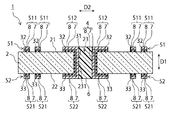
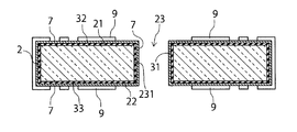
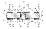
先ず、図1を参照しながら、本開示の貫通電極基板の一例について説明する。図1は、本実施形態による貫通電極基板1を示す断面図である。本実施形態の貫通電極基板1は、例えば、光学用途のインターポーザ基板に用いることができる。 First, an example of the through silicon via substrate of the present disclosure will be described with reference to FIG. FIG. 1 is a cross-sectional view showing a through silicon via substrate 1 according to the present embodiment. The through silicon via substrate 1 of the present embodiment can be used, for example, as an interposer substrate for optical applications.

図1に示すように、本実施形態の貫通電極基板1は、透明基板2と、第1密着層の一例である側壁密着層31と、第2密着層の一例である第1面密着層32および第2面密着層33と、貫通電極4と、導電層の一例である第1面導電層51および第2面導電層52と、有機層6と、を備える。 As shown in FIG. 1, the through electrode substrate 1 of the present embodiment includes a transparent substrate 2, a side wall adhesion layer 31 which is an example of a first adhesion layer, and a first surface adhesion layer 32 which is an example of a second adhesion layer. A second surface adhesive layer 33, a through electrode 4, an first surface conductive layer 51 and a second surface conductive layer 52, which are examples of the conductive layer, and an organic layer 6 are provided.

(透明基板2)
透明基板2は、可視光に対する透過性を有する基板であり、例えば、石英ガラス、無アルカリガラス、ソーダライムガラス、パイレックス(登録商標)ガラス、合成石英板等の可撓性のない透明なリジッド材が挙げられる。この種の透明基板2は、透明性が要求される貫通電極基板1に好適に用いることができる。特に無アルカリガラスは信頼性とコストの点で好ましい。
(Transparent substrate 2)
The transparent substrate 2 is a substrate having transparency to visible light, and is a non-flexible transparent rigid material such as quartz glass, non-alkali glass, soda lime glass, Pyrex (registered trademark) glass, and synthetic quartz plate. Can be mentioned. This type of transparent substrate 2 can be suitably used for the through silicon via substrate 1 that requires transparency. In particular, non-alkali glass is preferable in terms of reliability and cost.

透明基板2は、第1表面21と、第1表面21の反対側の第2表面22とを有する。図1の例において、第1表面21と第2表面22とは互いに平行である。透明基板2の内部に貫通電極4を位置させるため、透明基板2には、第1表面21から第2表面22まで透明基板2を貫通する貫通孔23が設けられている。 The transparent substrate 2 has a first surface 21 and a second surface 22 on the opposite side of the first surface 21. In the example of FIG. 1, the first surface 21 and the second surface 22 are parallel to each other. In order to position the through electrode 4 inside the transparent substrate 2, the transparent substrate 2 is provided with a through hole 23 penetrating the transparent substrate 2 from the first surface 21 to the second surface 22.

貫通孔23は、第1表面21に直交すなわち交差する透明基板2の厚み方向D1に垂直な断面において円形状を有する。また、図示はしないが、貫通孔23は、第1表面21に沿った第1表面21の面方向D2に間隔を空けて複数設けられている。 The through hole 23 has a circular shape in a cross section perpendicular to the thickness direction D1 of the transparent substrate 2 orthogonal to or intersecting the first surface 21. Further, although not shown, a plurality of through holes 23 are provided at intervals in the surface direction D2 of the first surface 21 along the first surface 21.

また、図1の例において、貫通孔23の内径は、第1表面21から第2表面22に至るまで殆ど変化しない。すなわち、図1の貫通孔23は、厚み方向D1に沿ってストレートな円筒形状の側壁231を有している。後述の図10(a)〜図10(c)に示すように、貫通孔23の内径は、第1表面21および第2表面22の一方から他方に向かって変化してもよい。 Further, in the example of FIG. 1, the inner diameter of the through hole 23 hardly changes from the first surface 21 to the second surface 22. That is, the through hole 23 in FIG. 1 has a cylindrical side wall 231 that is straight along the thickness direction D1. As shown in FIGS. 10 (a) to 10 (c) described later, the inner diameter of the through hole 23 may change from one of the first surface 21 and the second surface 22 toward the other.

貫通孔23は、面方向D2の寸法すなわち内径φに対する厚みTの比T/φであるアスペクト比が、3以上33以下であることが望ましい。一例として、貫通孔23の内径φは、15μm以上100μm以下であり、貫通孔23の厚みTは、300μm以上500μm以下である。貫通孔23のアスペクト比T/φを3以上とすることで、貫通孔23の内径φを抑制できるので、貫通電極4の配線密度を高めることができる。貫通孔23のアスペクト比T/φを33以下とすることで、貫通孔23の内部に貫通電極4を形成するために十分な内径φを確保することができる。 It is desirable that the through hole 23 has an aspect ratio of 3 or more and 33 or less, which is the ratio T / φ of the thickness T to the dimension of the surface direction D2, that is, the inner diameter φ. As an example, the inner diameter φ of the through hole 23 is 15 μm or more and 100 μm or less, and the thickness T of the through hole 23 is 300 μm or more and 500 μm or less. By setting the aspect ratio T / φ of the through hole 23 to 3 or more, the inner diameter φ of the through hole 23 can be suppressed, so that the wiring density of the through electrode 4 can be increased. By setting the aspect ratio T / φ of the through hole 23 to 33 or less, it is possible to secure a sufficient inner diameter φ for forming the through electrode 4 inside the through hole 23.

(側壁密着層31)
側壁密着層31は、貫通孔23の側壁231上に位置し、透明基板2および貫通電極4の双方への密着性および絶縁性を有する層である。
(Side wall contact layer 31)
The side wall contact layer 31 is located on the side wall 231 of the through hole 23 and has adhesion and insulation to both the transparent substrate 2 and the through electrode 4.

側壁密着層31を介した透明基板2と貫通電極4との密着性は、側壁密着層31が無い場合の透明基板2と貫通電極4との直接的な密着性より高い。このような密着性の大小関係は、側壁密着層31を介して側壁231上に形成した貫通電極4を剥離することを模擬した剥離試験と、側壁231上に直接形成した貫通電極4を剥離することを模擬した剥離試験とを実施し、双方の剥離試験における剥離力を比較することで確認することができる。剥離試験としては、JIS H 8504に規定されているめっきの密着性試験方法のうち、テープ試験を用いることができる。テープ試験は、めっき皮膜に粘着力のあるテープを貼り付けて急速に引き剥がす試験である。テープを引き剥がすとき、めっき皮膜の密着性が悪いほど、テープ粘着面に付着するめっき皮膜の量、すなわちめっき皮膜の剥離量が多くなる。めっき皮膜の剥離量が多いほど、めっき皮膜の剥離に要する剥離力は小さい。テープ試験によれば、透明基板上に密着層を介して形成されためっき皮膜にテープを貼り付けて引き剥がした場合のめっき皮膜の剥離量と、透明基板上に直接形成されためっき皮膜にテープを貼り付けて引き剥がした場合のめっき皮膜の剥離量とを比較することで、密着層の有無に応じた剥離力を比較することができる。 The adhesion between the transparent substrate 2 and the through electrode 4 via the side wall contact layer 31 is higher than the direct adhesion between the transparent substrate 2 and the through electrode 4 when the side wall contact layer 31 is absent. The magnitude relationship of such adhesion is a peeling test simulating peeling of the through electrode 4 formed on the side wall 231 via the side wall contact layer 31, and peeling of the through electrode 4 formed directly on the side wall 231. It can be confirmed by carrying out a peeling test simulating this and comparing the peeling forces in both peeling tests. As the peeling test, a tape test can be used among the plating adhesion test methods specified in JIS H 8504. The tape test is a test in which an adhesive tape is attached to a plating film and rapidly peeled off. When the tape is peeled off, the poorer the adhesion of the plating film, the larger the amount of the plating film adhering to the adhesive surface of the tape, that is, the amount of the plating film peeled off. The larger the amount of peeling of the plating film, the smaller the peeling force required for peeling the plating film. According to the tape test, the amount of peeling of the plating film when the tape is attached and peeled off from the plating film formed on the transparent substrate via the adhesion layer, and the tape on the plating film directly formed on the transparent substrate. By comparing the amount of peeling of the plating film when the plating film is pasted and peeled off, it is possible to compare the peeling force depending on the presence or absence of the adhesive layer.

なお、密着層の大小関係は、実施例において説明する「JIS K5600 塗料一般試験方法」に規定されているクロスカット試験法によって確認することもできる。 The magnitude relationship of the adhesive layer can also be confirmed by the cross-cut test method specified in the "JIS K5600 paint general test method" described in the examples.

側壁密着層31は、有機物を含有する。有機物を含有することで、側壁密着層31は、
透明基板2および貫通電極4との間で高い密着性を発揮することができる。
The side wall contact layer 31 contains an organic substance. By containing an organic substance, the side wall adhesion layer 31 is
High adhesion can be exhibited between the transparent substrate 2 and the through silicon via 4.

側壁密着層31に含有される有機物は、側壁密着層31上に無電解めっき法で貫通電極4のシード層を形成する場合における金属析出性と薬液耐性との双方を有することが望ましい。このような有機物としては、例えば、エポキシ樹脂、アクリル樹脂、ポリイミド樹脂、ウレタン樹脂などの高分子樹脂を好適に用いることができる。なお、高分子樹脂は、無機酸化膜や有機単分子膜と比較して、側壁231上に均一に側壁密着層31が形成されているか否かを判断し易いので、生産性の向上に寄与することもできる。 It is desirable that the organic substance contained in the side wall contact layer 31 has both metal precipitation property and chemical solution resistance when the seed layer of the through electrode 4 is formed on the side wall contact layer 31 by an electroless plating method. As such an organic substance, for example, a polymer resin such as an epoxy resin, an acrylic resin, a polyimide resin, or a urethane resin can be preferably used. Compared with the inorganic oxide film and the organic monomolecular film, the polymer resin makes it easier to determine whether or not the side wall adhesion layer 31 is uniformly formed on the side wall 231 and thus contributes to the improvement of productivity. You can also do it.

側壁密着層31の厚みは、15nm以上200nm以下であることが望ましい。側壁密着層31の厚みを15nm以上とすることで、側壁密着層31上に無電解めっき法で貫通電極4のシード層を形成する場合に、側壁密着層31に十分な量の触媒を吸着させることができるので、貫通電極4のシード層の析出性を向上させることができる。側壁密着層31の厚みを200nm以下とすることで、無電解めっきの後工程として実施される各種の加熱工程において側壁密着層31から発生するガスの総量を抑制することができるので、ガスの圧力による貫通電極4の変形およびこれにともなう電気的特性の悪化を抑制することができる。 The thickness of the side wall contact layer 31 is preferably 15 nm or more and 200 nm or less. By setting the thickness of the side wall contact layer 31 to 15 nm or more, a sufficient amount of catalyst is adsorbed on the side wall contact layer 31 when the seed layer of the through electrode 4 is formed on the side wall contact layer 31 by the electroless plating method. Therefore, the precipitation property of the seed layer of the through electrode 4 can be improved. By setting the thickness of the side wall contact layer 31 to 200 nm or less, the total amount of gas generated from the side wall contact layer 31 can be suppressed in various heating steps performed as a subsequent step of electroless plating, so that the pressure of the gas can be suppressed. It is possible to suppress the deformation of the penetrating electrode 4 due to the above and the deterioration of the electrical characteristics accompanying the deformation.

側壁密着層31は、例えば、ディップコート、スプレーコート、およびスピンコートなどのウェットプロセスを用いて形成してもよい。 The side wall adhesion layer 31 may be formed using, for example, a wet process such as dip coating, spray coating, and spin coating.

(第1面密着層32)
第1面密着層32は、第1表面21上に位置し、透明基板2および第1面導電層51の双方への密着性および絶縁性を有する層である。
(First surface adhesion layer 32)
The first surface adhesion layer 32 is a layer that is located on the first surface 21 and has adhesion and insulation to both the transparent substrate 2 and the first surface conductive layer 51.

第1面密着層32を介した透明基板2と第1面導電層51との密着性は、第1面密着層32が無い場合の透明基板2と第1面導電層51との直接的な密着性より高い。このような密着性の大小関係は、第1面密着層32を介して第1表面21上に形成した第1面導電層51を剥離することを模擬した剥離試験と、第1表面21上に直接形成した第1面導電層51を剥離することを模擬した剥離試験とを実施し、双方の剥離試験における第1面導電層51の剥離力を比較することで確認することができる。剥離試験としては、JIS H 8504に規定されているめっきの密着性試験方法のうち、テープ試験、または、「JIS K5600 塗料一般試験方法」に規定されているクロスカット試験法を用いることができる。 The adhesion between the transparent substrate 2 and the first surface conductive layer 51 via the first surface adhesion layer 32 is directly between the transparent substrate 2 and the first surface conductive layer 51 when the first surface adhesion layer 32 is absent. Higher than adhesion. The magnitude relationship of such adhesion is determined by a peeling test simulating peeling of the first surface conductive layer 51 formed on the first surface 21 via the first surface contact layer 32 and a peeling test on the first surface 21. It can be confirmed by carrying out a peeling test simulating peeling of the directly formed first surface conductive layer 51 and comparing the peeling forces of the first surface conductive layer 51 in both peeling tests. As the peeling test, among the plating adhesion test methods specified in JIS H 8504, the tape test or the cross-cut test method specified in "JIS K5600 paint general test method" can be used.

側壁密着層31と同様に、第1面密着層32は、有機物を含有する。有機物を含有することで、第1面密着層32は、透明基板2および第1面導電層51との間で高い密着性を発揮することができる。 Similar to the side wall contact layer 31, the first surface contact layer 32 contains an organic substance. By containing an organic substance, the first surface adhesion layer 32 can exhibit high adhesion between the transparent substrate 2 and the first surface conductive layer 51.

側壁密着層31と同様に、第1面密着層32に含有される有機物は、第1面密着層32上に無電解めっき法で第1面導電層51のシード層を形成する場合における金属析出性と薬液耐性との双方を有することが望ましい。このような有機物としては、例えば、エポキシ樹脂、アクリル樹脂、ポリイミド樹脂、ウレタン樹脂などの高分子樹脂を好適に用いることができる。なお、高分子樹脂は、無機酸化膜や有機単分子膜と比較して第1表面21上に均一に第1面密着層32が形成されているか否かを判断し易いので、生産性の向上に寄与することもできる。 Similar to the side wall adhesion layer 31, the organic matter contained in the first surface adhesion layer 32 is metal-precipitated when the seed layer of the first surface conductive layer 51 is formed on the first surface adhesion layer 32 by an electroless plating method. It is desirable to have both sex and chemical resistance. As such an organic substance, for example, a polymer resin such as an epoxy resin, an acrylic resin, a polyimide resin, or a urethane resin can be preferably used. In the polymer resin, it is easier to determine whether or not the first surface adhesion layer 32 is uniformly formed on the first surface 21 as compared with the inorganic oxide film or the organic monomolecular film, so that the productivity is improved. Can also contribute to.

側壁密着層31と同様に、第1面密着層32の厚みは、15nm以上200nm以下であることが望ましい。第1面密着層32の厚みを15nm以上とすることで、第1面密着層32上に無電解めっき法で第1面導電層51のシード層を形成する場合に、第1面密着層32に十分な量の触媒を吸着させることができるので、第1面導電層51のシード層の析出性を向上させることができる。第1面密着層32の厚みを200nm以下とすることで、無電解めっき後の加熱工程において第1面密着層32から発生するガスの総量を抑制することができるので、ガスの圧力による第1面導電層51の膨張およびこれにともなう電気的特性の悪化を抑制することができる。 Similar to the side wall contact layer 31, the thickness of the first surface contact layer 32 is preferably 15 nm or more and 200 nm or less. When the seed layer of the first surface conductive layer 51 is formed on the first surface adhesive layer 32 by the electroless plating method by setting the thickness of the first surface adhesive layer 32 to 15 nm or more, the first surface adhesive layer 32 Since a sufficient amount of catalyst can be adsorbed on the surface, the precipitation property of the seed layer of the first surface conductive layer 51 can be improved. By setting the thickness of the first surface adhesion layer 32 to 200 nm or less, the total amount of gas generated from the first surface adhesion layer 32 in the heating step after electroless plating can be suppressed, so that the first due to the pressure of the gas can be suppressed. It is possible to suppress the expansion of the surface conductive layer 51 and the accompanying deterioration of electrical characteristics.

第1面密着層32は、後述する第1面導電層51の複数の第1面配線部511および第1面パッド部512に対応するように、面方向D2に間隔を空けて部分的に第1表面21上に位置している。したがって、複数の第1面配線部511間には第1面密着層32が存在しない。このような構成によれば、後述する複数の第1面配線部511間におけるマイグレーションを抑制することができる。 The first surface contact layer 32 is partially separated in the surface direction D2 so as to correspond to a plurality of first surface wiring portions 511 and first surface pad portions 512 of the first surface conductive layer 51, which will be described later. It is located on one surface 21. Therefore, the first surface contact layer 32 does not exist between the plurality of first surface wiring portions 511. According to such a configuration, migration between a plurality of first surface wiring portions 511, which will be described later, can be suppressed.

第1面密着層32は、例えば、ディップコート、スプレーコート、およびスピンコートなどのウェットプロセスによって側壁密着層31と同一材料で同時に形成してもよい。 The first surface adhesion layer 32 may be simultaneously formed of the same material as the side wall adhesion layer 31 by a wet process such as dip coating, spray coating, and spin coating.

(第2面密着層33)
第2面密着層33は、第2表面22上に位置し、透明基板2および第2面導電層52の双方への密着性および絶縁性を有する層である。
(Second surface adhesion layer 33)
The second surface adhesion layer 33 is located on the second surface 22 and has adhesion and insulation to both the transparent substrate 2 and the second surface conductive layer 52.

第2面密着層33を介した透明基板2と第2面導電層52との密着性は、第2面密着層33が無い場合の透明基板2と第2面導電層52との直接的な密着性より高い。このような密着性の大小関係は、第2面密着層33を介して第2表面22上に形成した第2面導電層52を剥離することを模擬した剥離試験と、第2表面22上に直接形成した第2面導電層52を剥離することを模擬した剥離試験とを実施し、双方の剥離試験における第2面導電層52の剥離力を比較することで確認することができる。剥離試験としては、JIS H 8504に規定されているめっきの密着性試験方法のうち、テープ試験、または、「JIS K5600 塗料一般試験方法」に規定されているクロスカット試験法を用いることができる。 The adhesion between the transparent substrate 2 and the second surface conductive layer 52 via the second surface adhesion layer 33 is directly between the transparent substrate 2 and the second surface conductive layer 52 when the second surface adhesion layer 33 is absent. Higher than adhesion. The magnitude relationship of such adhesion is determined by a peeling test simulating peeling of the second surface conductive layer 52 formed on the second surface 22 via the second surface contact layer 33 and a peeling test on the second surface 22. It can be confirmed by carrying out a peeling test simulating peeling of the directly formed second surface conductive layer 52 and comparing the peeling forces of the second surface conductive layer 52 in both peeling tests. As the peeling test, among the plating adhesion test methods specified in JIS H 8504, the tape test or the cross-cut test method specified in "JIS K5600 paint general test method" can be used.

側壁密着層31と同様に、第2面密着層33は、有機物を含有する。有機物を含有することで、第2面密着層33は、透明基板2および第2面導電層52との間で高い密着性を発揮することができる。 Like the side wall contact layer 31, the second surface contact layer 33 contains an organic substance. By containing an organic substance, the second surface adhesion layer 33 can exhibit high adhesion between the transparent substrate 2 and the second surface conductive layer 52.

側壁密着層31と同様に、第2面密着層33に含有される有機物は、第2面密着層33上に無電解めっき法で第2面導電層52のシード層を形成する場合における金属析出性と薬液耐性との双方を有することが望ましい。このような有機物としては、例えば、エポキシ樹脂、アクリル樹脂、ポリイミド樹脂、ウレタン樹脂などの高分子樹脂を好適に用いることができる。なお、高分子樹脂は、無機酸化膜や有機単分子膜と比較して第2表面22上に均一に第2面密着層33が形成されているか否かを判断し易いので、生産性の向上に寄与することもできる。 Similar to the side wall adhesion layer 31, the organic matter contained in the second surface adhesion layer 33 is metal-precipitated when the seed layer of the second surface conductive layer 52 is formed on the second surface adhesion layer 33 by the electroless plating method. It is desirable to have both sex and chemical resistance. As such an organic substance, for example, a polymer resin such as an epoxy resin, an acrylic resin, a polyimide resin, or a urethane resin can be preferably used. In the polymer resin, it is easier to determine whether or not the second surface adhesion layer 33 is uniformly formed on the second surface 22 as compared with the inorganic oxide film or the organic monomolecular film, so that the productivity is improved. Can also contribute to.

側壁密着層31と同様に、第2面密着層33の厚みは、15nm以上200nm以下であることが望ましい。第2面密着層33の厚みを15nm以上とすることで、第2面密着層33上に無電解めっき法で第2面導電層52のシード層を形成する場合に、第2面密着層33に十分な量の触媒を吸着させることができるので、第2面導電層52のシード層の析出性を向上させることができる。第2面密着層33の厚みを200nm以下とすることで、無電解めっき後の加熱工程において第2面密着層33から発生するガスの総量を抑制することができるので、ガスの圧力による第2面導電層52の膨張およびこれにともなう電気的特性の悪化を抑制することができる。 Similar to the side wall contact layer 31, the thickness of the second surface contact layer 33 is preferably 15 nm or more and 200 nm or less. When the seed layer of the second surface conductive layer 52 is formed on the second surface adhesive layer 33 by the electroless plating method by setting the thickness of the second surface adhesive layer 33 to 15 nm or more, the second surface adhesive layer 33 Since a sufficient amount of catalyst can be adsorbed on the surface, the precipitation property of the seed layer of the second surface conductive layer 52 can be improved. By setting the thickness of the second surface adhesion layer 33 to 200 nm or less, the total amount of gas generated from the second surface adhesion layer 33 in the heating step after electroless plating can be suppressed, so that the second surface adhesion layer 33 is affected by the pressure of the gas. It is possible to suppress the expansion of the surface conductive layer 52 and the accompanying deterioration of electrical characteristics.

第2面密着層33は、後述する第2面導電層52の複数の第2面配線部521および第2面パッド部522に対応するように、面方向D2に間隔を空けて部分的に第2表面22上に位置している。したがって、複数の第2面配線部521間には第2面密着層33が存在しない。このような構成によれば、後述する複数の第2面配線部521間におけるマイグレーションを抑制することができる。 The second surface contact layer 33 is partially separated in the surface direction D2 so as to correspond to a plurality of second surface wiring portions 521 and second surface pad portions 522 of the second surface conductive layer 52, which will be described later. 2 Located on the surface 22. Therefore, the second surface contact layer 33 does not exist between the plurality of second surface wiring portions 521. According to such a configuration, migration between a plurality of second surface wiring portions 521, which will be described later, can be suppressed.

第2面密着層33は、例えば、ディップコート、スプレーコート、およびスピンコートなどのウェットプロセスによって側壁密着層31および第1面密着層32と同一材料で同時に形成してもよい。 The second surface adhesion layer 33 may be simultaneously formed of the same material as the side wall adhesion layer 31 and the first surface adhesion layer 32 by a wet process such as dip coating, spray coating, and spin coating.

(貫通電極4)
貫通電極4は、貫通孔23の内部において側壁密着層31上に位置し、且つ導電性を有する部材である。図1の例において、貫通電極4の厚みは、貫通孔23の幅すなわち内径よりも小さく、このため、貫通孔23の内部には、貫通電極4が存在しない空間がある。すなわち、貫通電極4は、いわゆるコンフォーマルビアである。なお、図1の例において、貫通孔23の内部の空間は、貫通電極4の内側に位置する有機層6で埋められている。
(Through Silicon Via 4)
The through electrode 4 is a member that is located on the side wall contact layer 31 inside the through hole 23 and has conductivity. In the example of FIG. 1, the thickness of the through electrode 4 is smaller than the width of the through hole 23, that is, the inner diameter, and therefore, there is a space inside the through hole 23 in which the through electrode 4 does not exist. That is, the through electrode 4 is a so-called conformal via. In the example of FIG. 1, the space inside the through hole 23 is filled with the organic layer 6 located inside the through electrode 4.

図1に示すように、貫通電極4は、第3導電層の一例として、側壁密着層31上に位置するシード層7と、第4導電層の一例として、シード層7上に位置するめっき層8とを有する。 As shown in FIG. 1, the through silicon via 4 has a seed layer 7 located on the side wall adhesion layer 31 as an example of the third conductive layer, and a plating layer located on the seed layer 7 as an example of the fourth conductive layer. Has 8 and.

シード層7は、電解めっき法によってめっき層8を形成する電解めっき工程の際に、めっき液中の金属イオンを析出させてめっき層8を成長させるための土台となる、導電性を有する層である。 The seed layer 7 is a conductive layer that serves as a base for growing the plating layer 8 by precipitating metal ions in the plating solution during the electrolytic plating step of forming the plating layer 8 by the electrolytic plating method. is there.

シード層7の材料としては、銅などの導電性を有する材料を用いることができる。シード層7の材料は、めっき層8の材料と同一であってもよく、異なっていてもよい。例えば、シード層7は、チタンと銅を順に積層した積層膜や、クロムなどであってもよい。シード層7は、例えば、無電解めっき法で形成することができる。 As the material of the seed layer 7, a conductive material such as copper can be used. The material of the seed layer 7 may be the same as or different from the material of the plating layer 8. For example, the seed layer 7 may be a laminated film in which titanium and copper are laminated in this order, chromium, or the like. The seed layer 7 can be formed by, for example, an electroless plating method.

めっき層8は、電解めっき法によって形成される、導電性を有する層である。めっき層8は、例えば、銅を含有する。めっき層8は、銅と、銅以外の金属、例えば、金、銀、白金、ロジウム、スズ、アルミニウム、ニッケル、クロムとの合金を含有していてもよく、または、銅と銅以外の金属とを積層したものであってもよい。 The plating layer 8 is a conductive layer formed by an electrolytic plating method. The plating layer 8 contains, for example, copper. The plating layer 8 may contain an alloy of copper and a metal other than copper, for example, gold, silver, platinum, rhodium, tin, aluminum, nickel, chromium, or copper and a metal other than copper. May be laminated.

また、シード層7およびめっき層8は、タングステン、チタン、タンタルその他の高融点化合物を主成分として含有していてもよい。 Further, the seed layer 7 and the plating layer 8 may contain tungsten, titanium, tantalum or other refractory compound as a main component.

(第1面導電層51)
第1面導電層51は、第1面密着層32上に位置し、且つ導電性を有する層である。第1面導電層51は、複数の第1面配線部511と、第1面パッド部512とを有する。
(1st surface conductive layer 51)
The first surface conductive layer 51 is a layer that is located on the first surface adhesion layer 32 and has conductivity. The first surface conductive layer 51 has a plurality of first surface wiring portions 511 and a first surface pad portion 512.

第1面パッド部512は、貫通電極4と電気的に接続されており、より具体的には、貫通孔23の第1表面21側の周縁部上において、貫通電極4の第1表面21側の端部に連続している。第1面パッド部512は、平面視した場合に貫通孔23と同心の円環形状を呈していてもよい。貫通電極4と同様に、第1面パッド部512は、第1導電層の一例として、第1面密着層32上に位置するシード層7と、第2導電層の一例として、シード層7上に位置するめっき層8とを有する。第1面パッド部512のシード層7およびめっき層8は、貫通電極4のシード層7およびめっき層8と共通、すなわち同一成分を含有する。なお、貫通電極4と第1面パッド部512との境界部において、第1面パッド部512に覆われた第1面密着層32は、側壁密着層31に連続している。第1面密着層32が側壁密着層31に連続していることで、透明基板2の中で比較的にめっき不良が起こり易い角部上に位置する第1面パッド部512についても、透明基板2への密着性を可及的に向上させることができる。 The first surface pad portion 512 is electrically connected to the through electrode 4, and more specifically, on the peripheral edge portion of the through hole 23 on the first surface 21 side, the first surface 21 side of the through electrode 4 It is continuous with the end of. The first surface pad portion 512 may have an annular shape concentric with the through hole 23 when viewed in a plan view. Similar to the through silicon via 4, the first surface pad portion 512 is provided on the seed layer 7 located on the first surface adhesion layer 32 as an example of the first conductive layer and on the seed layer 7 as an example of the second conductive layer. It has a plating layer 8 located at. The seed layer 7 and the plating layer 8 of the first surface pad portion 512 are common to the seed layer 7 and the plating layer 8 of the through electrode 4, that is, contain the same components. At the boundary between the through electrode 4 and the first surface pad portion 512, the first surface adhesion layer 32 covered with the first surface pad portion 512 is continuous with the side wall adhesion layer 31. Since the first surface adhesion layer 32 is continuous with the side wall adhesion layer 31, the transparent substrate also has the first surface pad portion 512 located on the corner portion where plating failure is relatively likely to occur in the transparent substrate 2. Adhesion to 2 can be improved as much as possible.

複数の第1面配線部511は、面方向D2に間隔を空けて第1面密着層32上に位置する。各第1面配線部511の少なくとも1つは、貫通電極4と電気的に接続されていてもよい。貫通電極4と同様に、各第1面配線部511は、第1導電層の一例として、第1面密着層32上に位置するシード層7と、第2導電層の一例として、シード層7上に位置するめっき層8とを有する。第1面配線部511のシード層7およびめっき層8は、貫通電極4のシード層7およびめっき層8と共通、すなわち同一成分を含有する。 The plurality of first surface wiring portions 511 are located on the first surface adhesion layer 32 at intervals in the surface direction D2. At least one of the first surface wiring portions 511 may be electrically connected to the through electrode 4. Similar to the through silicon via 4, each first surface wiring portion 511 has a seed layer 7 located on the first surface adhesion layer 32 as an example of the first conductive layer, and a seed layer 7 as an example of the second conductive layer. It has a plating layer 8 located on top. The seed layer 7 and the plating layer 8 of the first surface wiring portion 511 share the same components as the seed layer 7 and the plating layer 8 of the through electrode 4.

なお、各第1面配線部511に覆われた第1面密着層32は、各第1面配線部511のそれぞれに対応するように面方向D2に間隔を空けて第1表面21上に位置する。図1の例において、隣り合う第1面配線部511同士の間には第1面密着層32が存在しない。これにより、隣り合う第1面配線部511同士の間で、第1面密着層32の表面を伝った金属の移動によるマイグレーションが生じることを抑制することができる。 The first surface contact layer 32 covered with the first surface wiring portions 511 is located on the first surface 21 at intervals in the surface direction D2 so as to correspond to each of the first surface wiring portions 511. To do. In the example of FIG. 1, the first surface contact layer 32 does not exist between the adjacent first surface wiring portions 511. As a result, it is possible to suppress the occurrence of migration due to the movement of the metal along the surface of the first surface adhesion layer 32 between the adjacent first surface wiring portions 511.

(第2面導電層52)
第2面導電層52は、第2面密着層33上に位置し、且つ導電性を有する層である。第2面導電層52は、複数の第2面配線部521と、第2面パッド部522とを有する。
(Second surface conductive layer 52)
The second surface conductive layer 52 is a layer that is located on the second surface adhesion layer 33 and has conductivity. The second surface conductive layer 52 has a plurality of second surface wiring portions 521 and a second surface pad portion 522.

第2面パッド部522は、貫通電極4と電気的に接続されており、より具体的には、貫通孔23の第2表面22側の周縁部上において、貫通電極4の第2表面22側の端部に連続している。第2面パッド部522は、平面視した場合に貫通孔23と同心の円環形状を呈していてもよい。貫通電極4と同様に、第2面パッド部522は、第1導電層の一例として、第2面密着層33上に位置するシード層7と、第2導電層の一例として、シード層7上に位置するめっき層8とを有する。第2面パッド部522のシード層7およびめっき層8は、貫通電極4のシード層7およびめっき層8と共通、すなわち同一成分を含有する。なお、貫通電極4と第2面パッド部522との境界部において、第2面パッド部522に覆われた第2面密着層33は、側壁密着層31に連続している。第2面密着層33が側壁密着層31に連続していることで、透明基板2の中で比較的にめっき不良が起こり易い角部上に位置する第2面パッド部522についても、透明基板2への密着性を可及的に向上させることができる。 The second surface pad portion 522 is electrically connected to the through electrode 4, and more specifically, on the peripheral edge portion of the through hole 23 on the second surface 22 side, the second surface 22 side of the through electrode 4. It is continuous with the end of. The second surface pad portion 522 may have an annular shape concentric with the through hole 23 when viewed in a plan view. Similar to the through silicon via 4, the second surface pad portion 522 has a seed layer 7 located on the second surface adhesion layer 33 as an example of the first conductive layer, and a seed layer 7 as an example of the second conductive layer. It has a plating layer 8 located at. The seed layer 7 and the plating layer 8 of the second surface pad portion 522 are common to the seed layer 7 and the plating layer 8 of the through electrode 4, that is, contain the same components. At the boundary between the through electrode 4 and the second surface pad portion 522, the second surface contact layer 33 covered with the second surface pad portion 522 is continuous with the side wall contact layer 31. Since the second surface adhesion layer 33 is continuous with the side wall adhesion layer 31, the transparent substrate also has the second surface pad portion 522 located on the corner portion where plating failure is relatively likely to occur in the transparent substrate 2. Adhesion to 2 can be improved as much as possible.

複数の第2面配線部521は、面方向D2に間隔を空けて第2面密着層33上に位置する。各第2面配線部521の少なくとも1つは、貫通電極4と電気的に接続されていてもよい。貫通電極4と同様に、各第2面配線部521は、第1導電層の一例として、第2面密着層33上に位置するシード層7と、第2導電層の一例として、シード層7上に位置するめっき層8とを有する。第2面配線部521のシード層7およびめっき層8は、貫通電極4のシード層7およびめっき層8と共通、すなわち同一成分を含有する。 The plurality of second surface wiring portions 521 are located on the second surface adhesion layer 33 at intervals in the surface direction D2. At least one of the second surface wiring portions 521 may be electrically connected to the through electrode 4. Similar to the through silicon via 4, each second surface wiring portion 521 has a seed layer 7 located on the second surface adhesion layer 33 as an example of the first conductive layer, and a seed layer 7 as an example of the second conductive layer. It has a plating layer 8 located on top. The seed layer 7 and the plating layer 8 of the second surface wiring portion 521 are common to the seed layer 7 and the plating layer 8 of the through electrode 4, that is, contain the same components.

なお、各第2面配線部521に覆われた第2面密着層33は、各第2面配線部521のそれぞれに対応するように面方向D2に間隔を空けて第2表面22上に位置する。図1の例において、隣り合う第2面配線部521同士の間には第2面密着層33が存在しない。これにより、第2面配線部521同士の間で、第2面密着層33の表面を伝った金属の移動によるマイグレーションが生じることを抑制することができる。 The second surface contact layer 33 covered with the second surface wiring portions 521 is located on the second surface 22 at intervals in the surface direction D2 so as to correspond to each of the second surface wiring portions 521. To do. In the example of FIG. 1, the second surface contact layer 33 does not exist between the adjacent second surface wiring portions 521. As a result, it is possible to prevent migration due to the movement of the metal along the surface of the second surface adhesion layer 33 between the second surface wiring portions 521.

(有機層6)
有機層6は、貫通孔23の内部に位置する、絶縁性を有する層である。有機層6の有機材料としては、ポリイミドやエポキシ樹脂などを用いることができる。
(Organic layer 6)
The organic layer 6 is an insulating layer located inside the through hole 23. As the organic material of the organic layer 6, polyimide, epoxy resin or the like can be used.

(貫通電極基板1の製造方法)
以下、貫通電極基板1の製造方法の一例について、図1乃至図9を参照して説明する。
(Manufacturing Method of Through Silicon Via Substrate 1)
Hereinafter, an example of a method for manufacturing the through silicon via
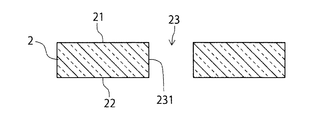
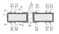
 substrate 1 will be described with reference to FIGS. 1 to 9.

(貫通孔形成工程)
図2は、本実施形態による貫通電極基板1の製造方法を示す断面図である。まず、透明基板2を準備する。透明基板2を準備した後、図2に示すように、第1表面21から第2表面22まで透明基板2を貫通する貫通孔23を透明基板2に形成する。貫通孔23の形成方法としては、例えば、レーザ照射を用いることができる。レーザとしては、エキシマレーザ、Nd:YAGレーザ、フェムト秒レーザ等を用いることができる。Nd:YAGレーザを採用する場合、波長が1064nmの基本波、波長が532nmの第2高調波、波長が355nmの第3高調波等を用いることができる。
(Through hole forming process)
FIG. 2 is a cross-sectional view showing a method of manufacturing the through silicon via substrate 1 according to the present embodiment. First, the transparent substrate 2 is prepared. After preparing the transparent substrate 2, as shown in FIG. 2, a through hole 23 penetrating the transparent substrate 2 from the first surface 21 to the second surface 22 is formed in the transparent substrate 2. As a method for forming the through hole 23, for example, laser irradiation can be used. As the laser, an excimer laser, an Nd: YAG laser, a femtosecond laser, or the like can be used. When the Nd: YAG laser is adopted, a fundamental wave having a wavelength of 1064 nm, a second harmonic having a wavelength of 532 nm, a third harmonic having a wavelength of 355 nm, and the like can be used.

また、レーザ照射とウェットエッチングを適宜組み合わせることもできる。具体的には、まず、レーザ照射によって透明基板2のうち貫通孔23が形成されるべき領域に変質層を形成する。続いて、透明基板2をフッ化水素などに浸漬して、変質層をエッチングする。これによって、透明基板2に貫通孔23を形成することができる。 Further, laser irradiation and wet etching can be appropriately combined. Specifically, first, the altered layer is formed in the region of the transparent substrate 2 where the through hole 23 should be formed by laser irradiation. Subsequently, the transparent substrate 2 is immersed in hydrogen fluoride or the like to etch the altered layer. As a result, the through hole 23 can be formed in the transparent substrate 2.

レーザ照射以外にも、透明基板2に研磨材を吹き付けるブラスト処理や、反応性イオンエッチング法、深掘り反応性イオンエッチング法などのドライエッチング法などによって透明基板2に貫通孔23を形成してもよい。 In addition to laser irradiation, even if a through
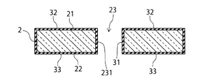
 hole 23 is formed in the transparent substrate 2 by a blast treatment of spraying an abrasive on the transparent substrate 2, a dry etching method such as a reactive ion etching method or a deep digging reactive ion etching method, or the like. Good.

(密着層形成工程)
図3は、図2に続く本実施形態による貫通電極基板1の製造方法を示す断面図である。貫通孔23を形成した後、図3に示すように、貫通孔23の側壁231上への側壁密着層31の形成と、第1表面21上への第1面密着層32の形成と、第2表面22上への第2面密着層33の形成とを行う。密着層31〜33は、例えば、15〜200nmの厚みに形成する。密着層31〜33の形成は、例えば、ディップコート、スプレーコートまたはスピンコートなどのウェットプロセスで行うことができる。このうち、ディップコートによれば、すべての密着層31〜33を同時に形成することができるので、製造効率を向上させることができる。
(Adhesion layer forming process)
FIG. 3 is a cross-sectional view showing a method of manufacturing the through silicon via
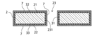
 substrate 1 according to the present embodiment following FIG. After forming the through hole 23, as shown in FIG. 3, the side wall adhesion layer 31 is formed on the side wall 231 of the through hole 23, the first surface adhesion layer 32 is formed on the first surface 21, and the first surface adhesion layer 32 is formed. The second surface adhesion layer 33 is formed on the two surfaces 22. The adhesion layers 31 to 33 are formed to have a thickness of, for example, 15 to 200 nm. The formation of the adhesion layers 31 to 33 can be performed by a wet process such as dip coating, spray coating or spin coating. Of these, according to the dip coat, all the adhesion layers 31 to 33 can be formed at the same time, so that the production efficiency can be improved.

(シード層形成工程)
図4は、図3に続く本実施形態による貫通電極基板1の製造方法を示す断面図である。密着層31〜33を形成した後、図4に示すように、密着層31〜33上にシード層7を形成する。シード層7は、例えば200〜500nmの厚みに形成する。以下、密着層31〜33が形成された透明基板2のことを、単に透明基板2とも呼ぶ。
(Seed layer forming process)
FIG. 4 is a cross-sectional view showing a method of manufacturing the through silicon via substrate 1 according to the present embodiment following FIG. After forming the adhesion layers 31 to 33, the seed layer 7 is formed on the adhesion layers 31 to 33 as shown in FIG. The seed layer 7 is formed to have a thickness of, for example, 200 to 500 nm. Hereinafter, the transparent substrate 2 on which the adhesion layers 31 to 33 are formed is also simply referred to as a transparent substrate 2.

シード層7の形成においては、先ず、透明基板2を洗浄と、透明基板2の濡れ性を上げるための表面改質とを行う。洗浄および表面改質は、例えば、PH2以下の酸性水溶液またはPH11以上のアルカリ性水溶液を40〜50℃に保持し、当該酸性水浴液またはアルカリ性水溶液中に透明基板2を5〜15分間浸漬することで行うことができる。 In forming the seed layer 7, first, the transparent substrate 2 is cleaned and the surface of the transparent substrate 2 is modified to improve the wettability of the transparent substrate 2. For cleaning and surface modification, for example, an acidic aqueous solution having a pH of 2 or less or an alkaline aqueous solution having a pH of 11 or more is held at 40 to 50 ° C., and the transparent substrate 2 is immersed in the acidic water bath solution or the alkaline aqueous solution for 5 to 15 minutes. It can be carried out.

洗浄および表面改質を行った後、透明基板2を触媒化する。具体的には、無電解銅めっきの触媒となるPdイオンまたはSn/Pdコロイドを密着層31〜33に吸着させる。触媒化は、例えば、Pdイオンを含有するPH9〜11のアルカリ性水溶液またはSn/Pdコロイドを含有するPH2以下の酸性水溶液を40〜50℃に保持し、当該酸性水浴液またはアルカリ性水溶液中に透明基板2を5〜15分間浸漬することで行うことができる。 After cleaning and surface modification, the transparent substrate 2 is catalyzed. Specifically, Pd ions or Sn / Pd colloids, which are catalysts for electroless copper plating, are adsorbed on the adhesion layers 31 to 33. For catalysis, for example, an alkaline aqueous solution having a pH of 9 to 11 containing Pd ions or an acidic aqueous solution having a pH of 2 or less containing a Sn / Pd colloid is maintained at 40 to 50 ° C. This can be done by immersing 2 for 5 to 15 minutes.

触媒化を行った後、密着層31〜33に吸着させたPdイオンのPdへの還元または密着層31〜33に吸着させたSn/PdコロイドにおけるPdの活性化を行う。Pdの還元は、例えば、適当な還元剤を含むPH5〜8の水溶液を50℃に保持し、この水溶液中に透明基板2を1〜5分間浸漬することで行うことができる。Pdの活性化は、例えば、PH2以下の酸性水溶液またはPH11以上のアルカリ性水溶液を50℃に保持し、この水溶液中に透明基板2を1〜5分間浸漬することで行うことができる。 After catalysis, Pd ions adsorbed on the adhesion layers 31 to 33 are reduced to Pd or Pd is activated in the Sn / Pd colloid adsorbed on the adhesion layers 31 to 33. The reduction of Pd can be carried out, for example, by holding an aqueous solution of PH5 to 8 containing an appropriate reducing agent at 50 ° C. and immersing the transparent substrate 2 in the aqueous solution for 1 to 5 minutes. Activation of Pd can be carried out, for example, by holding an acidic aqueous solution having a pH of 2 or less or an alkaline aqueous solution having a pH of 11 or more at 50 ° C. and immersing the transparent substrate 2 in this aqueous solution for 1 to 5 minutes.

Pdイオンの還元またはPdの活性化を行った後、無電解銅めっきを行う。具体的には、密着層31〜33に吸着されたPdを触媒とし、密着層31〜33上に銅の被膜を形成する。無電解銅めっきは、例えば、銅イオン、水酸化ナトリウムおよびホルマリンを含有するアルカリ性水溶液を30〜40℃に保持し、このアルカリ性水溶液中に透明基板2を5〜30分間浸漬することで行うことができる。 After reducing Pd ions or activating Pd, electroless copper plating is performed. Specifically, Pd adsorbed on the adhesion layers 31 to 33 is used as a catalyst to form a copper film on the adhesion layers 31 to 33. Electroless copper plating can be performed, for example, by holding an alkaline aqueous solution containing copper ions, sodium hydroxide and formalin at 30 to 40 ° C. and immersing the transparent substrate 2 in the alkaline aqueous solution for 5 to 30 minutes. it can.

(レジスト層形成工程)
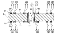
図5は、図4に続く本実施形態による貫通電極基板1の製造方法を示す断面図である。シード層7を形成した後、図5に示すように、貫通電極4、第1面導電層51および第2面導電層52を形成すべき一部の領域を除いて、シード層7上にレジスト層9を形成する。レジスト層9の形成は、例えば、シード層7上にドライフィルムレジストをラミネートし、ラミネートされたドライフィルムレジストを露光および現像することで行うことができる。
(Resist layer forming step)
FIG. 5 is a cross-sectional view showing a method of manufacturing the through silicon via substrate 1 according to the present embodiment following FIG. After forming the seed layer 7, as shown in FIG. 5, a resist is formed on the seed layer 7 except for a part of the region where the through electrode 4, the first surface conductive layer 51 and the second surface conductive layer 52 should be formed. The layer 9 is formed. The resist layer 9 can be formed, for example, by laminating a dry film resist on the seed layer 7 and exposing and developing the laminated dry film resist.

(めっき層形成工程)
図6は、図5に続く本実施形態による貫通電極基板1の製造方法を示す断面図である。レジスト層9を形成した後、図6に示すように、レジスト層9をマスクとした電解めっき法により、レジスト層9によって覆われていないシード層7上にめっき層8を形成する。めっき層8は、例えば2〜12μmの厚みに形成する。
(Plating layer forming process)
FIG. 6 is a cross-sectional view showing a method of manufacturing the through silicon via substrate 1 according to the present embodiment following FIG. After forming the resist layer 9, as shown in FIG. 6, the plating layer 8 is formed on the seed layer 7 not covered by the resist layer 9 by an electrolytic plating method using the resist layer 9 as a mask. The plating layer 8 is formed to have a thickness of, for example, 2 to 12 μm.

(レジスト層除去工程)
図7は、図6に続く本実施形態による貫通電極基板1の製造方法を示す断面図である。めっき層8を形成した後、図7に示すように、透明基板2からレジスト層9を剥離すなわち除去する。レジスト層9は、例えば、アルカリ溶液への浸漬で除去することができる。
(Resist layer removal process)
FIG. 7 is a cross-sectional view showing a method of manufacturing the through silicon via substrate 1 according to the present embodiment following FIG. After forming the plating layer 8, as shown in FIG. 7, the resist layer 9 is peeled off or removed from the transparent substrate 2. The resist layer 9 can be removed, for example, by immersing it in an alkaline solution.

(シード層除去工程)
図8は、図7に続く本実施形態による貫通電極基板1の製造方法を示す断面図である。レジスト層9を除去した後、図8に示すように、シード層7のうちレジスト層9が形成されていた部分を除去する。シード層7は、例えば、ウェットエッチングで除去することができる。シード層7を除去することで、貫通電極4と、第1面導電層51と、第2面導電層52とが同時に形成される。
(Seed layer removal process)
FIG. 8 is a cross-sectional view showing a method of manufacturing the through silicon via substrate 1 according to the present embodiment following FIG. After removing the resist layer 9, as shown in FIG. 8, the portion of the seed layer 7 on which the resist layer 9 is formed is removed. The seed layer 7 can be removed by, for example, wet etching. By removing the seed layer 7, the through electrode 4, the first surface conductive layer 51, and the second surface conductive layer 52 are formed at the same time.

(密着層除去工程)
図9は、図8に続く本実施形態による貫通電極基板1の製造方法を示す断面図である。シード層7を除去した後、図9に示すように、第1面密着層32のうち第1面導電層51で覆われていない部分を除去するとともに、第2面密着層33のうち第2面導電層52で覆われていない部分を除去する。密着層32、33は、例えば、プラズマアッシングやアルカリ浸漬などで除去することができる。
(Adhesion layer removal process)
FIG. 9 is a cross-sectional view showing a method of manufacturing the through silicon via substrate 1 according to the present embodiment following FIG. After removing the seed layer 7, as shown in FIG. 9, the portion of the first surface adhesive layer 32 that is not covered with the first surface conductive layer 51 is removed, and the second of the second surface adhesive layer 33 is removed. The portion not covered by the surface conductive layer 52 is removed. The adhesion layers 32 and 33 can be removed by, for example, plasma ashing or alkaline immersion.

(有機層形成工程)
密着層32、33を除去した後、図1に示すように、貫通孔23の内部に有機層6を形成する。具体的には、先ず、有機層6を構成するための樹脂層を含むフィルムを、透明基板2の第1表面21上及び第2表面22上に配置する。次いで、フィルムを加圧することにより、樹脂層を貫通孔23の内部に押し込む。その後、貫通孔23の内部に押し込まれた樹脂層を、樹脂層に光を照射することなどによって硬化させる。また、樹脂層の不要部分を除去する。このようにして、貫通孔23の内部に有機層6を設けることができる。
(Organic layer forming process)
After removing the adhesion layers 32 and 33, the organic layer 6 is formed inside the through hole 23 as shown in FIG. Specifically, first, a film containing a resin layer for forming the organic layer 6 is arranged on the first surface 21 and the second surface 22 of the transparent substrate 2. Then, by pressurizing the film, the resin layer is pushed into the through hole 23. After that, the resin layer pushed into the through hole 23 is cured by irradiating the resin layer with light or the like. In addition, the unnecessary portion of the resin layer is removed. In this way, the organic layer 6 can be provided inside the through hole 23.

(実施例)
以下、本実施形態の実施例として、貫通電極基板1の試料に対して実施した観察および電気検査の結果について説明する。
(Example)
Hereinafter, as an example of this embodiment, the results of observation and electrical inspection performed on the sample of the through silicon via substrate 1 will be described.

実施例では、密着層の厚みが互いに異なる試料No.1〜No.7の7つの試料を作製した。各試料の作製にあたっては、先ず、各試料に共通の透明基板2として、厚み450μmの無アルカリガラスに90μmφすなわちアスペクト比:5の貫通孔23を形成した透明基板2を準備した。 In the examples, the sample Nos. 1-No. Seven samples of 7 were prepared. In preparing each sample, first, as a transparent substrate 2 common to each sample, a transparent substrate 2 having a through hole 23 having a thickness of 450 μm and a through hole 23 having a thickness of 90 μmφ, that is, an aspect ratio of 5 was prepared.

透明基板2上への密着層31〜33の形成においては、ポリイミドを主成分とする有機樹脂を、各試料毎にディップコートの有無または速度を変えて異なる厚みに形成した。具体的には、試料No.1については、ディップコートを行わず、密着層31〜33を形成しなかった。その他の試料の密着層31〜33の厚みは、試料No.2については15nm、試料No.3については22nm、試料No.4については98nm、試料No.5については185nm、試料No.6については203nm、試料No.7については210nmとした。 In the formation of the adhesion layers 31 to 33 on the transparent substrate 2, an organic resin containing polyimide as a main component was formed to have different thicknesses for each sample by changing the presence or absence of dip coating or the speed. Specifically, the sample No. For No. 1, no dip coating was performed and the adhesion layers 31 to 33 were not formed. The thickness of the adhesion layers 31 to 33 of the other samples is the sample No. For 2, 15 nm, sample No. For No. 3, 22 nm, sample No. For No. 4, 98 nm, sample No. For 5, 185 nm, sample No. For No. 6, 203 nm, sample No. 7 was set to 210 nm.

シード層7の形成においては、各試料とも、無電解めっき法によって500nmの厚みを有するようにシード層7を形成した。 In the formation of the seed layer 7, the seed layer 7 was formed so that each sample had a thickness of 500 nm by an electroless plating method.

シード層7上へのレジスト層9の形成においては、各試料とも、日立化成社製のRY5319をラミネートした後、膜表面から100μm離れた位置にフォトマスクを配置して、プロキシミティアライナにより、超高圧水銀ランプでパターン露光した。パターン露光後、液温30℃、濃度1%の炭酸ナトリウム水溶液中に透明基板2を1分間浸漬して現像を行うことで、レジスト層9の未硬化部分を除去した。 In the formation of the resist layer 9 on the seed layer 7, each sample was laminated with RY5319 manufactured by Hitachi Chemical Co., Ltd., and then a photomask was placed at a position 100 μm away from the film surface, and a proximity liner was used to superimpose the resist layer 9. The pattern was exposed with a high-pressure mercury lamp. After the pattern exposure, the uncured portion of the resist layer 9 was removed by immersing the transparent substrate 2 in a sodium carbonate aqueous solution having a liquid temperature of 30 ° C. and a concentration of 1% for 1 minute for development.

シード層7上へのめっき層8の形成においては、各試料とも、電解銅めっき法によって、レジスト層9で覆われていないシード層7上に5μmの厚みを有するように、めっき層8を形成した。 In the formation of the plating layer 8 on the seed layer 7, the plating layer 8 is formed on the seed layer 7 not covered with the resist layer 9 by the electrolytic copper plating method so that each sample has a thickness of 5 μm. did.

めっき層8の形成後のレジスト層9の除去においては、各試料とも、濃度3%の水酸化ナトリウム水溶液を用いて3分間のスプレー剥離を行うことで、透明基板2からレジスト層9を剥離した。 In the removal of the resist layer 9 after the formation of the plating layer 8, the resist layer 9 was peeled from the transparent substrate 2 by spray peeling for 3 minutes using an aqueous solution of sodium hydroxide having a concentration of 3% for each sample. ..

レジスト層9の除去後のシード層7の除去においては、各試料とも、銅除去剤であるメック社製SF−5420に透明基板2を1分間浸漬するウェットエッチングを行うことで、シード層7を除去した。 In the removal of the seed layer 7 after the removal of the resist layer 9, each sample is subjected to wet etching in which the transparent substrate 2 is immersed in SF-5420 manufactured by MEC, which is a copper removing agent, for 1 minute to obtain the seed layer 7. Removed.

シード層7の除去後の密着層32、33の除去においては、プラズマ照射により、めっき層8で覆われていない配線部間および配線部とパッド部との間の密着層32、33を除去した。 In the removal of the adhesion layers 32 and 33 after the removal of the seed layer 7, the adhesion layers 32 and 33 between the wiring portions and between the wiring portions and the pad portions not covered by the plating layer 8 were removed by plasma irradiation. ..

密着層32、33の除去後は、各試料とも、窒素雰囲気下において200℃で30分間のアニール処理を行った。 After the adhesion layers 32 and 33 were removed, each sample was annealed at 200 ° C. for 30 minutes in a nitrogen atmosphere.

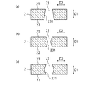
以上のようにして作製された試料No.1〜No.7に対して、シード層の析出状態の観察と、アニール処理後のシード層の膨張状態の観察と、「JIS K5600 塗料一般試験方法」に規定されているクロスカット試験法によるシード層の剥離状態の観察とを行った。観察には、電子顕微鏡を使用した。また、電気検査として、シード層による電気信号の導通検査を行った。なお、クロスカット試験法は、既述したテープ試験と類似している。クロスカット試験法では、シード層が形成された透明基板の試験面に、カッターで透明基板に達する碁盤目状の切り傷を形成する。そして、碁盤目部分にテープを強く圧着させ、テープの端を45°の角度で一気に引き剥がし、碁盤目部分の状態を標準図と比較して評価する。 実施例の観察結果および電気検査結果を以下の表1および図10(a)〜図10(c)に示す。 The sample No. prepared as described above. 1-No. 7: Observation of the precipitation state of the seed layer, observation of the expansion state of the seed layer after annealing treatment, and the peeling state of the seed layer by the cross-cut test method specified in "JIS K5600 General Paint Test Method". Was observed. An electron microscope was used for the observation. In addition, as an electrical inspection, a continuity inspection of the electrical signal by the seed layer was performed. The cross-cut test method is similar to the tape test described above. In the cross-cut test method, a grid-like cut that reaches the transparent substrate with a cutter is formed on the test surface of the transparent substrate on which the seed layer is formed. Then, the tape is strongly crimped to the grid portion, the end of the tape is peeled off at a stretch at an angle of 45 °, and the state of the grid portion is evaluated by comparing with the standard drawing. The observation results and electrical inspection results of the examples are shown in Table 1 and FIGS. 10 (a) to 10 (c) below.

Figure 0006889855
Figure 0006889855

表1中の“○”は、結果が良好であることを示している。一方、表1中の“×”は、結果が悪いことを示している。また、図10(a)は、試料No.2〜試料No.6に示される本実施形態による貫通電極基板1において、透明基板2上へのシード層7の形成状態を模式的に示す平面図である。図10(b)は、試料No.1に示される第1の比較例による貫通電極基板において、透明基板2上へのシード層7の形成状態を模式的に示す平面図である。図10(c)は、試料No.7に示される第2の比較例による貫通電極基板において、透明基板2上へのシード層7の形成状態を模式的に示す平面図である。 “○” in Table 1 indicates that the result is good. On the other hand, "x" in Table 1 indicates that the result is bad. Further, FIG. 10 (a) shows the sample No. 2-Sample No. 6 is a plan view schematically showing a state in which a seed layer 7 is formed on a transparent substrate 2 in the through silicon via substrate 1 according to the present embodiment shown in 6. FIG. 10B shows the sample No. FIG. 5 is a plan view schematically showing a state in which a seed layer 7 is formed on a transparent substrate 2 in the through silicon via substrate according to the first comparative example shown in 1. FIG. 10 (c) shows the sample No. 7 is a plan view schematically showing a state in which the seed layer 7 is formed on the transparent substrate 2 in the through silicon via substrate according to the second comparative example shown in 7.

表1および図10(a)に示すように、試料No.2〜No.6においては、透明基板2上にシード層7が万遍なく形成され、アニールにともなうシード層7の膨張も殆ど無いことが確認された。更に、試料No.2〜No.6においては、クロスカット試験によるシード層7の剥離が殆ど無く、また、導通状態が良好であることが確認された。このような試料No.2〜試料No.6の結果は、試料No.2〜試料No.6が適度な厚みの密着層31〜33を有することで、シード層7の密着性を確保しつつアニールの際に密着層31〜33から生じるガスの総量を抑制できることによるものと推測される。 As shown in Table 1 and FIG. 10 (a), Sample Nos. 2 to No. In No. 6, it was confirmed that the seed layer 7 was evenly formed on the transparent substrate 2 and that there was almost no expansion of the seed layer 7 due to annealing. Further, Sample Nos. 2 to No. In No. 6, it was confirmed that the seed layer 7 was hardly peeled off by the cross-cut test and that the conduction state was good. Such sample No. 2-Sample No. The result of No. 6 is the sample No. 2-Sample No. It is presumed that the fact that 6 has the adhesion layers 31 to 33 having an appropriate thickness makes it possible to suppress the total amount of gas generated from the adhesion layers 31 to 33 at the time of annealing while ensuring the adhesion of the seed layer 7.

一方、試料No.1においては、表1および図10(b)に示すように、シード層7が形成されずに透明基板2が露出した箇所が確認された。更に、試料No.1においては、クロスカット試験によるシード層7の剥離量が多く、また、導通不良が生じることが確認された。このような試料No.1の結果は、試料No.1が密着層31〜33を有しないことで、シード層7の密着性を確保できないことによるものと推測される。 On the other hand, sample No. In No. 1, as shown in Table 1 and FIG. 10B, a portion where the transparent substrate 2 was exposed without the seed layer 7 being formed was confirmed. Furthermore, the sample No. In No. 1, it was confirmed that the amount of peeling of the seed layer 7 was large by the cross-cut test and that conduction failure occurred. Such sample No. The result of 1 is the sample No. It is presumed that the fact that 1 does not have the adhesion layers 31 to 33 makes it impossible to secure the adhesion of the seed layer 7.

また、試料No.7においては、表1および図10(c)に示すように、アニールにともなうシード層7の膨張部7aが多数生じることが確認された。更に、試料No.7においては、導通不良が生じることが確認された。このような試料No.7の結果は、試料No.7の密着層31〜33の厚みが過大であることで、アニールの際に密着層31〜33から生じるガスの総量が多いことによるものと推測される。 In addition, sample No. In No. 7, as shown in Table 1 and FIG. 10 (c), it was confirmed that a large number of expanded portions 7a of the seed layer 7 were generated due to annealing. Furthermore, the sample No. In No. 7, it was confirmed that poor continuity occurred. Such sample No. The result of 7 is the sample No. It is presumed that the excessive thickness of the close contact layers 31 to 33 of No. 7 is due to the large total amount of gas generated from the close contact layers 31 to 33 during annealing.

以上の実施例によれば、密着層31〜33の厚みを15nm以上200nm以下とすることで、シード層7の密着性および電気特性が良好になることが確認された。 According to the above examples, it was confirmed that the adhesion and electrical characteristics of the seed layer 7 were improved by setting the thickness of the adhesion layers 31 to 33 to 15 nm or more and 200 nm or less.

以下、本実施形態によってもたらされる作用について説明する。 Hereinafter, the action brought about by this embodiment will be described.

図1に示したように、本実施形態によれば、側壁密着層31と、第1面密着層32と、第2面密着層33とを備えることで、透明基板2と貫通電極4との密着性だけでなく、透明基板2と第1面導電層51および第2面導電層52との密着性も高めることができる。これにより、透明基板2からの貫通電極4および配線部511、521の剥離を同時に抑制することができる。 As shown in FIG. 1, according to the present embodiment, the transparent substrate 2 and the through electrode 4 are provided with the side wall contact layer 31, the first surface contact layer 32, and the second surface contact layer 33. Not only the adhesion but also the adhesion between the transparent substrate 2 and the first surface conductive layer 51 and the second surface conductive layer 52 can be improved. As a result, peeling of the through electrode 4 and the wiring portions 511 and 521 from the transparent substrate 2 can be suppressed at the same time.

また、本実施形態によれば、隣り合う配線部511、521間に密着層32、33が設けられていないため、隣り合う配線部511、521同士の間でのマイグレーションを抑制することができる。 Further, according to the present embodiment, since the close contact layers 32 and 33 are not provided between the adjacent wiring portions 511 and 521, migration between the adjacent wiring portions 511 and 521 can be suppressed.

また、貫通孔23のアスペクト比T/φを3以上33以下とすれば、貫通電極4の配線密度を高めることができるとともに、貫通孔23の内部に貫通電極4を形成するために十分な内径φを確保することができる。 Further, if the aspect ratio T / φ of the through hole 23 is 3 or more and 33 or less, the wiring density of the through electrode 4 can be increased, and the inner diameter is sufficient to form the through electrode 4 inside the through hole 23. φ can be secured.

また、密着層31〜33の厚みを15nm以上200nm以下とすれば、貫通孔23のアスペクト比が高い場合においてもシード層7の析出性を向上させることができ、また、加熱工程において密着層31〜33から発生したガスによる貫通電極4および配線部511、521の変形を抑制することができ、電気的特性の悪化を抑制することができる。 Further, if the thickness of the adhesion layers 31 to 33 is 15 nm or more and 200 nm or less, the precipitation property of the seed layer 7 can be improved even when the aspect ratio of the through holes 23 is high, and the adhesion layer 31 can be improved in the heating step. Deformation of the through electrode 4 and the wiring portions 511 and 521 due to the gas generated from ~ 33 can be suppressed, and deterioration of electrical characteristics can be suppressed.

(第1の変形例)
次に、第1の変形例として、貫通孔23の形状の変形例について説明する。図11(a)は、本実施形態の第1の変形例による貫通電極基板1として、貫通孔23の一変形例を示す断面図である。図11(b)は、図11(a)と異なる貫通孔23の変形例を示す断面図である。図11(c)は、図11(a)および図11(b)と異なる貫通孔23の変形例を示す断面図である。
(First modification)
Next, as a first modification, a modification of the shape of the through hole 23 will be described. FIG. 11A is a cross-sectional view showing a modified example of the through hole 23 as the through electrode substrate 1 according to the first modified example of the present embodiment. FIG. 11B is a cross-sectional view showing a modified example of the through hole 23 different from that of FIG. 11A. FIG. 11 (c) is a cross-sectional view showing a modified example of the through hole 23 different from FIGS. 11 (a) and 11 (b).

図1の例において、貫通孔23の側壁231は、厚み方向D1の位置によらず内径が均一の円筒形状を有している。しかしながら、貫通孔23の形状が特に限られることはない。例えば、図11(a)に示すように、貫通孔23の側壁231は、第1表面21および第2表面22の一方から他方に向かうにしたがって内径が漸増するテーパ形状を有していてもよい。また、図11(b)に示すように、貫通孔23の側壁231は、第1表面21および第2表面22から透明基板2の厚み方向D1の中央部に向かうにしたがって内径が漸減する形状を有していてもよい。また、図11(c)に示すように、貫通孔23の側壁231は、第1表面21および第2表面22から透明基板2の厚み方向D1の中央部に向かうにしたがって内径が漸増する形状を有していてもよい。また、貫通孔23の面方向D2の断面は、円形状に限らず、例えば、多角形状であってもよい。 In the example of FIG. 1, the side wall 231 of the through hole 23 has a cylindrical shape having a uniform inner diameter regardless of the position in the thickness direction D1. However, the shape of the through hole 23 is not particularly limited. For example, as shown in FIG. 11A, the side wall 231 of the through hole 23 may have a tapered shape in which the inner diameter gradually increases from one of the first surface 21 and the second surface 22 toward the other. .. Further, as shown in FIG. 11B, the side wall 231 of the through hole 23 has a shape in which the inner diameter gradually decreases from the first surface 21 and the second surface 22 toward the central portion of the transparent substrate 2 in the thickness direction D1. You may have. Further, as shown in FIG. 11C, the side wall 231 of the through hole 23 has a shape in which the inner diameter gradually increases from the first surface 21 and the second surface 22 toward the central portion of the transparent substrate 2 in the thickness direction D1. You may have. Further, the cross section of the through hole 23 in the surface direction D2 is not limited to a circular shape, and may be, for example, a polygonal shape.

第1の変形例においても、図1の例と同様に、側壁密着層31と、第1面密着層32と、第2面密着層33とを備えることで、透明基板2からの貫通電極4および配線部511、521の剥離を同時に抑制することができる。 In the first modification, as in the example of FIG. 1, the through silicon via 4 from the transparent substrate 2 is provided with the side wall contact layer 31, the first surface contact layer 32, and the second surface contact layer 33. And the peeling of the wiring portions 511 and 521 can be suppressed at the same time.

(第2の変形例)
次に、第1面密着層32および第2面密着層33が全面的に形成された第2の変形例について説明する。図12は、本実施形態の第2の変形例による貫通電極基板1を示す断面図である。図1の例において、第1面密着層32は、第1面導電層51に対応するように第1表面21上に部分的に位置し、第2面密着層33は、第2面導電層52に対応するように第2表面22上に部分的に位置している。すなわち、第1面密着層32は、第1面導電層51が存在しない第1表面21上には設けられておらず、第2面密着層33は、第2面導電層52が存在しない第2表面22上には設けられていない。
(Second modification)
Next, a second modification in which the first surface adhesion layer 32 and the second surface adhesion layer 33 are completely formed will be described. FIG. 12 is a cross-sectional view showing the through silicon via substrate 1 according to the second modification of the present embodiment. In the example of FIG. 1, the first surface adhesive layer 32 is partially located on the first surface 21 so as to correspond to the first surface conductive layer 51, and the second surface adhesive layer 33 is the second surface conductive layer. It is partially located on the second surface 22 so as to correspond to 52. That is, the first surface adhesive layer 32 is not provided on the first surface 21 where the first surface conductive layer 51 does not exist, and the second surface adhesive layer 33 does not have the second surface conductive layer 52. 2 Not provided on the surface 22.

これに対して、第2の変形例の第1面密着層32は、図12に示すように、第1表面21上に全面的に位置している。また、第2面密着層33は、第2表面22上に全面的に位置している。 On the other hand, as shown in FIG. 12, the first surface contact layer 32 of the second modification is entirely located on the first surface 21. Further, the second surface adhesion layer 33 is entirely located on the second surface 22.

第2の変形例によれば、図9に示した密着層32、33の除去工程が不要となるので、製造工数を削減することができる。 According to the second modification, the steps of removing the adhesion layers 32 and 33 shown in FIG. 9 are not required, so that the manufacturing man-hours can be reduced.

(第3の変形例)
次に、導電層51、52が密着層32、33の側壁を覆う第3の変形例について説明する。図13は、本実施形態の第3の変形例による貫通電極基板1を示す断面図である。
(Third variant)
Next, a third modification in which the conductive layers 51 and 52 cover the side walls of the close contact layers 32 and 33 will be described. FIG. 13 is a cross-sectional view showing the through silicon via substrate 1 according to the third modification of the present embodiment.

図1の例において、第1面導電層51は、第1面密着層32に対して厚み方向D1の一方すなわち上方にのみ位置し、第2面導電層52は、第2面密着層33に対して厚み方向D1の他方すなわち下方のみに位置していた。 In the example of FIG. 1, the first surface conductive layer 51 is located only on one side, that is, above the thickness direction D1 with respect to the first surface adhesion layer 32, and the second surface conductive layer 52 is on the second surface adhesion layer 33. On the other hand, it was located only on the other side of the thickness direction D1, that is, below.

これに対して、第3の変形例の第1面導電層51は、図13に示すように、第1面密着層32に対して厚み方向D1の一方に位置する第1部分51aと、第1面密着層32に対して面方向D2に位置する第2部分51bとを有している。第2部分51bは、第1面密着層32の側壁を覆っている。 On the other hand, as shown in FIG. 13, the first surface conductive layer 51 of the third modification has the first portion 51a located on one side of the thickness direction D1 with respect to the first surface adhesion layer 32 and the first portion 51a. It has a second portion 51b located in the surface direction D2 with respect to the one-side contact layer 32. The second portion 51b covers the side wall of the first surface contact layer 32.

また、図13に示すように、第2面導電層52は、第2面密着層33に対して厚み方向D1の他方に位置する第1部分52aと、第2面密着層33に対して面方向D2に位置する第2部分52bとを有している。第2部分52bは、第2面密着層33の側壁を覆っている。 Further, as shown in FIG. 13, the second surface conductive layer 52 is a surface with respect to the first portion 52a located on the other side of the thickness direction D1 with respect to the second surface adhesion layer 33 and the second surface adhesion layer 33. It has a second portion 52b located in the direction D2. The second portion 52b covers the side wall of the second surface contact layer 33.

第3の変形例の貫通電極基板1は、密着層31〜33をパターニングした後にシード層7およびめっき層8を形成することによって製造することができる。 The through silicon via substrate 1 of the third modification can be manufactured by patterning the adhesion layers 31 to 33 and then forming the seed layer 7 and the plating layer 8.

第3の変形例によれば、第1面導電層51および第2面導電層52の断面積を増加することができるので、配線抵抗を低減することができる。 According to the third modification, the cross-sectional area of the first surface conductive layer 51 and the second surface conductive layer 52 can be increased, so that the wiring resistance can be reduced.

第1〜第3の変形例は、これらを適宜組み合わせてもよい。 In the first to third modifications, these may be combined as appropriate.
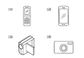
(製品への適用例)
図14は、上記各態様の貫通電極基板1を適用できる製品の例を示す図である。本開示の実施形態に係る貫通電極基板1は、光学用途の様々な製品に適用できる。例えば、貫通電極基板1は、携帯電話110のカメラ、スマートフォン120のカメラ、デジタルビデオカメラ130、デジタルカメラ140等に搭載できる。
(Example of application to products)
FIG. 14 is a diagram showing an example of a product to which the through silicon via substrate 1 of each of the above aspects can be applied. The through silicon via substrate 1 according to the embodiment of the present disclosure can be applied to various products for optical applications. For example, the through silicon via substrate 1 can be mounted on a camera of a mobile phone 110, a camera of a smartphone 120, a digital video camera 130, a digital camera 140, or the like.

本開示の態様は、上述した個々の実施形態に限定されるものではなく、当業者が想到しうる種々の変形も含むものであり、本開示の効果も上述した内容に限定されない。すなわち、特許請求の範囲に規定された内容およびその均等物から導き出される本開示の概念的な思想と趣旨を逸脱しない範囲で種々の追加、変更および部分的削除が可能である。 The aspects of the present disclosure are not limited to the individual embodiments described above, but also include various modifications that can be conceived by those skilled in the art, and the effects of the present disclosure are not limited to the contents described above. That is, various additions, changes and partial deletions are possible without departing from the conceptual idea and purpose of the present disclosure derived from the contents defined in the claims and their equivalents.

1 貫通電極基板
2 透明基板
21 第1表面
22 第2表面
23 貫通孔
31 側壁密着層
32 第1面密着層
33 第2面密着層
4 貫通電極
51 第1面導電層
52 第2面導電層
1 Through Electrode Substrate 2 Transparent Substrate 21 First Surface 22 Second Surface 23 Through Hole 31 Side Wall Adhesion Layer 32 First Surface Adhesion Layer 33 Second Surface Adhesion Layer 4 Through Electrode 51 First Surface Conductive Layer 52 Second Surface Conductive Layer

Claims (13)

第1表面と、前記第1表面の反対側の第2表面とを有し、前記第1表面から前記第2表面まで貫通する貫通孔が設けられた透明基板と、
前記貫通孔の側壁上に位置する第1密着層と、
前記第1表面上および前記第2表面上の少なくとも一方に少なくとも部分的に位置する第2密着層と、
前記第1密着層上に位置する貫通電極と、
前記第2密着層上に位置する導電層と、を備え
前記第1密着層および前記第2密着層は、15nm以上200nm以下の厚みを有する、貫通電極基板。
A transparent substrate having a first surface and a second surface opposite to the first surface and provided with through holes penetrating from the first surface to the second surface.
With the first adhesion layer located on the side wall of the through hole,
A second adhesion layer located at least partially on the first surface and at least one of the second surfaces.
Through silicon vias located on the first adhesion layer,
A conductive layer located on the second adhesion layer is provided .
Said first contact layer and said second adhesive layer is that having a 200nm thickness of not less than 15 nm, the through electrode substrate.
前記第1密着層を介した前記透明基板と前記貫通電極との密着性は、前記透明基板と前記貫通電極との直接的な密着性より高く、
前記第2密着層を介した前記透明基板と前記導電層との密着性は、前記透明基板と前記導電層との直接的な密着性より高い、請求項1に記載の貫通電極基板。
The adhesion between the transparent substrate and the through electrode via the first adhesion layer is higher than the direct adhesion between the transparent substrate and the through electrode.
The through electrode substrate according to claim 1, wherein the adhesion between the transparent substrate and the conductive layer via the second adhesion layer is higher than the direct adhesion between the transparent substrate and the conductive layer.
前記第1密着層および前記第2密着層は、有機物を含有する、請求項1または2に記載の貫通電極基板。 The through silicon via substrate according to claim 1 or 2, wherein the first adhesion layer and the second adhesion layer contain an organic substance. 前記貫通孔は、前記第1表面に沿った面方向の寸法に対する前記第1表面に交差する厚み方向の寸法の比であるアスペクト比が、3以上33以下である、請求項1乃至のいずれか一項に記載の貫通電極基板。 Any of claims 1 to 3 , wherein the through hole has an aspect ratio of 3 or more and 33 or less, which is a ratio of the dimension in the thickness direction intersecting the first surface to the dimension in the surface direction along the first surface. The through electrode substrate according to claim 1. 前記導電層は、前記第1表面に沿った面方向に間隔を空けて位置する複数の配線部を有し、
前記第2密着層は、前記導電層の前記複数の配線部のそれぞれに対応するように前記第1表面上および前記第2表面上の少なくとも一方に部分的に位置する、請求項1乃至のいずれか一項に記載の貫通電極基板。
The conductive layer has a plurality of wiring portions located at intervals in the surface direction along the first surface.
The second adhesion layer is partially located at least one on the first surface and the second surface so as to correspond to each of the plurality of wiring portions of the conductive layer, of claims 1 to 4 The through electrode substrate according to any one of the above.
前記導電層は、前記貫通孔の周縁部上において前記貫通電極に連続するパッド部を更に有し、
前記貫通電極と前記パッド部との境界部において、前記パッド部に覆われた前記第2密着層は、前記第1密着層に連続している、請求項に記載の貫通電極基板。
The conductive layer further has a pad portion continuous with the through electrode on the peripheral edge portion of the through hole.
The through electrode substrate according to claim 5 , wherein the second contact layer covered with the pad portion is continuous with the first contact layer at the boundary portion between the through electrode and the pad portion.
前記第1密着層と前記貫通電極との間および前記第2密着層と前記導電層との間に触媒が存在する、請求項1乃至のいずれか一項に記載の貫通電極基板。 The through electrode substrate according to any one of claims 1 to 6 , wherein a catalyst is present between the first contact layer and the through electrode and between the second contact layer and the conductive layer. 前記導電層は、前記第2密着層上に位置する第1導電層と、前記第1導電層上に位置する第2導電層と、を有する、請求項1乃至のいずれか一項に記載の貫通電極基板。 The invention according to any one of claims 1 to 7 , wherein the conductive layer has a first conductive layer located on the second adhesive layer and a second conductive layer located on the first conductive layer. Through electrode substrate. 前記貫通電極は、前記第1密着層上に位置し、前記第1導電層と同一の成分を含有する第3導電層と、前記第3導電層上に位置し、前記第2導電層と同一の成分を含有する第4導電層と、を有する、請求項に記載の貫通電極基板。 The through electrode is located on the first adhesive layer and contains the same components as the first conductive layer, and is located on the third conductive layer and is the same as the second conductive layer. The through silicon via substrate according to claim 8 , further comprising a fourth conductive layer containing the above-mentioned component. 前記第1導電層と前記第2導電層とは、同一の成分を含有する、請求項またはに記載の貫通電極基板。 The through silicon via substrate according to claim 8 or 9 , wherein the first conductive layer and the second conductive layer contain the same components. 前記透明基板は、ガラスを含有する、請求項1乃至10のいずれか一項に記載の貫通電極基板。 The through silicon via according to any one of claims 1 to 10 , wherein the transparent substrate contains glass. 第1表面と、前記第1表面の反対側の第2表面とを有する透明基板を準備する工程と、
前記透明基板に、前記第1表面から前記第2表面まで貫通する貫通孔を形成する工程と、
前記貫通孔の側壁上に第1密着層を形成する工程と、
前記第1表面上および前記第2表面上の少なくとも一方に、少なくとも部分的に第2密着層を形成する工程と、
前記第1密着層上に貫通電極を形成する工程と、
前記第2密着層上に導電層を形成する工程と、を備え
前記第1密着層および前記第2密着層は、15nm以上200nm以下の厚みを有するように形成する、貫通電極基板の製造方法。
A step of preparing a transparent substrate having a first surface and a second surface opposite to the first surface.
A step of forming a through hole penetrating from the first surface to the second surface on the transparent substrate, and
The step of forming the first adhesion layer on the side wall of the through hole and
A step of forming a second adhesion layer at least partially on the first surface and at least one of the second surfaces.
The step of forming a through electrode on the first adhesion layer and
A step of forming a conductive layer on the second adhesive layer is provided .
It said first contact layer and the second adhesion layer, you formed with a 200nm thickness of not less than 15 nm, the manufacturing method of the through electrode substrate.
前記貫通電極を形成する工程は、前記第1密着層上に触媒を付着させる工程と、前記触媒が付着された前記第1密着層上に無電解めっきを行う工程と、を有し、
前記導電層を形成する工程は、前記第2密着層上に触媒を付着させる工程と、前記触媒が付着された前記第2密着層上に無電解めっきを行う工程と、を有する、請求項12に記載の貫通電極基板の製造方法。
The step of forming the through electrode includes a step of adhering a catalyst on the first contact layer and a step of performing electroless plating on the first contact layer to which the catalyst is adhered.
The step of forming the conductive layer includes a step of adhering the catalyst to the second contact layer, and a step of performing electroless plating on said second contact layer, wherein the catalyst is attached, claim 12 The method for manufacturing a through electrode substrate according to.
JP2017070285A 2017-03-31 2017-03-31 Through Silicon Via Substrate and Its Manufacturing Method Active JP6889855B2 (en)

Priority Applications (1)

Application Number Priority Date Filing Date Title
JP2017070285A JP6889855B2 (en) 2017-03-31 2017-03-31 Through Silicon Via Substrate and Its Manufacturing Method

Applications Claiming Priority (1)

Application Number Priority Date Filing Date Title
JP2017070285A JP6889855B2 (en) 2017-03-31 2017-03-31 Through Silicon Via Substrate and Its Manufacturing Method

Publications (2)

Publication Number Publication Date
JP2018174190A JP2018174190A (en) 2018-11-08
JP6889855B2 true JP6889855B2 (en) 2021-06-18

Family

ID=64106633

Family Applications (1)

Application Number Title Priority Date Filing Date
JP2017070285A Active JP6889855B2 (en) 2017-03-31 2017-03-31 Through Silicon Via Substrate and Its Manufacturing Method

Country Status (1)

Country Link
JP (1) JP6889855B2 (en)

Families Citing this family (6)

* Cited by examiner, † Cited by third party
Publication number Priority date Publication date Assignee Title
KR102412292B1 (en) 2019-03-07 2022-06-22 앱솔릭스 인코포레이티드 Packaging substrate and semiconductor apparatus comprising same
CN113261094B (en) 2019-03-07 2024-04-16 爱玻索立克公司 Package substrate and semiconductor device including the same
US11967542B2 (en) 2019-03-12 2024-04-23 Absolics Inc. Packaging substrate, and semiconductor device comprising same
WO2020185020A1 (en) 2019-03-12 2020-09-17 에스케이씨 주식회사 Loading cassette for substrate including glass and substrate loading method to which same is applied
JP2022523898A (en) 2019-03-12 2022-04-27 アブソリックス インコーポレイテッド Packaging substrate and its manufacturing method
JP7746684B2 (en) * 2021-05-11 2025-10-01 大日本印刷株式会社 Through-hole electrode substrate

Family Cites Families (2)

* Cited by examiner, † Cited by third party
Publication number Priority date Publication date Assignee Title
WO2013150940A1 (en) * 2012-04-05 2013-10-10 旭硝子株式会社 Glass substrate with through electrode and method for producing glass substrate with through electrode
JP6467814B2 (en) * 2014-08-19 2019-02-13 凸版印刷株式会社 Wiring substrate manufacturing method and semiconductor device manufacturing method

Also Published As

Publication number Publication date
JP2018174190A (en) 2018-11-08

Similar Documents

Publication Publication Date Title
JP6889855B2 (en) Through Silicon Via Substrate and Its Manufacturing Method
JP2018174189A (en) Through electrode substrate and manufacturing method thereof
WO2019235617A1 (en) Method of manufacturing glass device and glass device
JP7171059B2 (en) Electronic component manufacturing method
TWI291221B (en) Printed circuit board, flip chip ball grid array board and method of fabricating the same
JP5350138B2 (en) Electric circuit manufacturing method and electric circuit board obtained by the method
US10553456B2 (en) Semiconductor package and manufacturing method of semiconductor package
KR20170123242A (en) Semiconductor package and manufacturing method thereof
US10224256B2 (en) Manufacturing method of semiconductor package
JP2018157051A (en) Method for manufacturing bump-attached wiring board
JP6078746B2 (en) Manufacturing method of vapor deposition mask
JP6819416B2 (en) Through Silicon Via Substrate and Its Manufacturing Method
JP6810908B2 (en) Conductive substrate and its manufacturing method
CN105023848A (en) Substrate structure and manufacturing method thereof
US20170358462A1 (en) Manufacturing method of semiconductor package
US10096564B2 (en) Manufacturing method of semiconductor package
JP2018174051A (en) Conductive substrate and manufacturing method thereof
JP5407161B2 (en) Multilayer circuit board manufacturing method
JP4705972B2 (en) Printed wiring board and manufacturing method thereof
CN1781348A (en) Printed wiring board, its manufacturing method, and circuit device
JP2007214338A (en) Manufacturing method of single-sided polyimide wiring board
US11343918B2 (en) Method of making printed circuit board and laminated structure
JP2005085898A (en) Method for manufacturing printed wiring board
JP2024009740A (en) Multilayer wiring board and its manufacturing method
JP2009267001A (en) Method for manufacturing wiring substrate

Legal Events

Date Code Title Description
A621 Written request for application examination

Free format text: JAPANESE INTERMEDIATE CODE: A621

Effective date: 20200130

A977 Report on retrieval

Free format text: JAPANESE INTERMEDIATE CODE: A971007

Effective date: 20201022

A131 Notification of reasons for refusal

Free format text: JAPANESE INTERMEDIATE CODE: A131

Effective date: 20201030

A521 Written amendment

Free format text: JAPANESE INTERMEDIATE CODE: A523

Effective date: 20201203

TRDD Decision of grant or rejection written
A01 Written decision to grant a patent or to grant a registration (utility model)

Free format text: JAPANESE INTERMEDIATE CODE: A01

Effective date: 20210423

A61 First payment of annual fees (during grant procedure)

Free format text: JAPANESE INTERMEDIATE CODE: A61

Effective date: 20210506

R150 Certificate of patent or registration of utility model

Ref document number: 6889855

Country of ref document: JP

Free format text: JAPANESE INTERMEDIATE CODE: R150