JP6884603B2 - Coil parts - Google Patents
Coil parts Download PDFInfo
- Publication number
- JP6884603B2 JP6884603B2 JP2017042938A JP2017042938A JP6884603B2 JP 6884603 B2 JP6884603 B2 JP 6884603B2 JP 2017042938 A JP2017042938 A JP 2017042938A JP 2017042938 A JP2017042938 A JP 2017042938A JP 6884603 B2 JP6884603 B2 JP 6884603B2
- Authority
- JP
- Japan
- Prior art keywords
- wire
- receiving portion
- terminal electrode
- central conductor
- welded
- Prior art date
- Legal status (The legal status is an assumption and is not a legal conclusion. Google has not performed a legal analysis and makes no representation as to the accuracy of the status listed.)
- Active
Links
- 239000004020 conductor Substances 0.000 claims description 53
- 238000004804 winding Methods 0.000 claims description 39
- 239000011247 coating layer Substances 0.000 claims description 36
- 239000000126 substance Substances 0.000 claims description 9
- 239000011347 resin Substances 0.000 claims description 6
- 229920005989 resin Polymers 0.000 claims description 6
- 239000010410 layer Substances 0.000 claims description 5
- 230000002093 peripheral effect Effects 0.000 claims description 4
- 229910000859 α-Fe Inorganic materials 0.000 description 38
- 238000003466 welding Methods 0.000 description 27
- 238000000034 method Methods 0.000 description 26
- 230000008569 process Effects 0.000 description 19
- 239000002184 metal Substances 0.000 description 17
- 229910052751 metal Inorganic materials 0.000 description 17
- 238000004891 communication Methods 0.000 description 9
- 239000000463 material Substances 0.000 description 7
- 230000004048 modification Effects 0.000 description 6
- 238000012986 modification Methods 0.000 description 6
- RYGMFSIKBFXOCR-UHFFFAOYSA-N Copper Chemical compound [Cu] RYGMFSIKBFXOCR-UHFFFAOYSA-N 0.000 description 5
- 230000000694 effects Effects 0.000 description 5
- 230000000630 rising effect Effects 0.000 description 5
- 229910052802 copper Inorganic materials 0.000 description 4
- 239000010949 copper Substances 0.000 description 4
- 230000000750 progressive effect Effects 0.000 description 4
- 239000000853 adhesive Substances 0.000 description 3
- 230000001070 adhesive effect Effects 0.000 description 3
- 230000002411 adverse Effects 0.000 description 3
- 230000008602 contraction Effects 0.000 description 3
- 238000010586 diagram Methods 0.000 description 3
- 230000035699 permeability Effects 0.000 description 3
- 229910000906 Bronze Inorganic materials 0.000 description 2
- OAICVXFJPJFONN-UHFFFAOYSA-N Phosphorus Chemical compound [P] OAICVXFJPJFONN-UHFFFAOYSA-N 0.000 description 2
- 229910045601 alloy Inorganic materials 0.000 description 2
- 239000000956 alloy Substances 0.000 description 2
- 230000004323 axial length Effects 0.000 description 2
- 239000010974 bronze Substances 0.000 description 2
- 238000006243 chemical reaction Methods 0.000 description 2
- 238000001816 cooling Methods 0.000 description 2
- KUNSUQLRTQLHQQ-UHFFFAOYSA-N copper tin Chemical compound [Cu].[Sn] KUNSUQLRTQLHQQ-UHFFFAOYSA-N 0.000 description 2
- 238000009413 insulation Methods 0.000 description 2
- 238000002844 melting Methods 0.000 description 2
- 230000008018 melting Effects 0.000 description 2
- 239000004962 Polyamide-imide Substances 0.000 description 1
- 230000008859 change Effects 0.000 description 1
- 230000003628 erosive effect Effects 0.000 description 1
- 238000010438 heat treatment Methods 0.000 description 1
- 238000003780 insertion Methods 0.000 description 1
- 230000037431 insertion Effects 0.000 description 1
- 238000004519 manufacturing process Methods 0.000 description 1
- 150000001247 metal acetylides Chemical class 0.000 description 1
- 229920002312 polyamide-imide Polymers 0.000 description 1
- 229920002635 polyurethane Polymers 0.000 description 1
- 239000004814 polyurethane Substances 0.000 description 1
- 238000003825 pressing Methods 0.000 description 1
- 238000004080 punching Methods 0.000 description 1
- 230000009467 reduction Effects 0.000 description 1
- 238000010008 shearing Methods 0.000 description 1
- 238000005476 soldering Methods 0.000 description 1
- 239000000758 substrate Substances 0.000 description 1
- 230000001629 suppression Effects 0.000 description 1
Images


Classifications
-
- H—ELECTRICITY
- H01—ELECTRIC ELEMENTS
- H01F—MAGNETS; INDUCTANCES; TRANSFORMERS; SELECTION OF MATERIALS FOR THEIR MAGNETIC PROPERTIES
- H01F5/00—Coils
- H01F5/06—Insulation of windings
-
- H—ELECTRICITY
- H01—ELECTRIC ELEMENTS
- H01F—MAGNETS; INDUCTANCES; TRANSFORMERS; SELECTION OF MATERIALS FOR THEIR MAGNETIC PROPERTIES
- H01F17/00—Fixed inductances of the signal type
- H01F17/04—Fixed inductances of the signal type with magnetic core
- H01F17/045—Fixed inductances of the signal type with magnetic core with core of cylindric geometry and coil wound along its longitudinal axis, i.e. rod or drum core
-
- H—ELECTRICITY
- H01—ELECTRIC ELEMENTS
- H01F—MAGNETS; INDUCTANCES; TRANSFORMERS; SELECTION OF MATERIALS FOR THEIR MAGNETIC PROPERTIES
- H01F27/00—Details of transformers or inductances, in general
- H01F27/24—Magnetic cores
-
- H—ELECTRICITY
- H01—ELECTRIC ELEMENTS
- H01F—MAGNETS; INDUCTANCES; TRANSFORMERS; SELECTION OF MATERIALS FOR THEIR MAGNETIC PROPERTIES
- H01F27/00—Details of transformers or inductances, in general
- H01F27/28—Coils; Windings; Conductive connections
- H01F27/2823—Wires
-
- H—ELECTRICITY
- H01—ELECTRIC ELEMENTS
- H01F—MAGNETS; INDUCTANCES; TRANSFORMERS; SELECTION OF MATERIALS FOR THEIR MAGNETIC PROPERTIES
- H01F27/00—Details of transformers or inductances, in general
- H01F27/28—Coils; Windings; Conductive connections
- H01F27/2823—Wires
- H01F27/2828—Construction of conductive connections, of leads
-
- H—ELECTRICITY
- H01—ELECTRIC ELEMENTS
- H01F—MAGNETS; INDUCTANCES; TRANSFORMERS; SELECTION OF MATERIALS FOR THEIR MAGNETIC PROPERTIES
- H01F27/00—Details of transformers or inductances, in general
- H01F27/28—Coils; Windings; Conductive connections
- H01F27/29—Terminals; Tapping arrangements for signal inductances
- H01F27/292—Surface mounted devices
-
- H—ELECTRICITY
- H01—ELECTRIC ELEMENTS
- H01F—MAGNETS; INDUCTANCES; TRANSFORMERS; SELECTION OF MATERIALS FOR THEIR MAGNETIC PROPERTIES
- H01F27/00—Details of transformers or inductances, in general
- H01F27/28—Coils; Windings; Conductive connections
- H01F27/32—Insulating of coils, windings, or parts thereof
- H01F27/322—Insulating of coils, windings, or parts thereof the insulation forming channels for circulation of the fluid
-
- H—ELECTRICITY
- H01—ELECTRIC ELEMENTS
- H01F—MAGNETS; INDUCTANCES; TRANSFORMERS; SELECTION OF MATERIALS FOR THEIR MAGNETIC PROPERTIES
- H01F27/00—Details of transformers or inductances, in general
- H01F27/34—Special means for preventing or reducing unwanted electric or magnetic effects, e.g. no-load losses, reactive currents, harmonics, oscillations, leakage fields
- H01F27/38—Auxiliary core members; Auxiliary coils or windings
-
- H—ELECTRICITY
- H01—ELECTRIC ELEMENTS
- H01F—MAGNETS; INDUCTANCES; TRANSFORMERS; SELECTION OF MATERIALS FOR THEIR MAGNETIC PROPERTIES
- H01F17/00—Fixed inductances of the signal type
- H01F2017/0093—Common mode choke coil
Description
この発明は、コイル部品に関するもので、特に、ワイヤと端子電極との接続構造に関するものである。 The present invention relates to a coil component, and more particularly to a connection structure between a wire and a terminal electrode.
この発明にとって興味ある技術として、たとえば特許第4184394号公報(特許文献1)に記載されたものがある。図12、図13および図14は、特許文献1から引用したもので、それぞれ、特許文献1における図2、図4および図5に相当する。図12ないし図14には、コイル部品に備えるコアの一部である一方の鍔部71およびそこに配置された端子電極72、ならびに端子電極72に接続されるワイヤ73の端部が図示されている。
As a technique of interest for the present invention, for example, there is one described in Japanese Patent No. 4184394 (Patent Document 1). 12, 13 and 14 are taken from
ワイヤ73は、図12および図14に示されるように、線状の中心導体74および中心導体74の周面を覆う絶縁被覆層75を備えている。端子電極72は、鍔部71の外側端面76側に配置された基部77と、基部77から屈曲部78を介して延びるもので、ワイヤ73の端部を受ける受け部79とを備えている。図12によく示されているように、端子電極72は、さらに、受け部79から第1の折返し部80を介して延びるもので、ワイヤ73の中心導体74に溶接される溶接片81と、受け部79から第2の折返し部82を介して延びるもので、ワイヤ73を保持して位置決めする保持部83とを備えている。
As shown in FIGS. 12 and 14, the
上述した溶接片81に関して、溶接工程を実施する前の状態が図12に示され、溶接工程後の状態が図13および図14に示されている。図13および図14には、溶接によって生じた膨出部84が図示されている。膨出部84は、溶接時において溶融した金属が表面張力により玉状となったまま冷却されて凝固して生成されたものであり、溶融玉とも称される。
With respect to the above-mentioned
溶接工程の詳細は、以下のとおりである。溶接工程の前の段階では、端子電極72において、溶接片81および保持部83は、受け部79に対して開いた状態にあり、受け部79とは対向していない。図12には、保持部83が受け部79と対向するが、溶接片81については受け部79に対して開いた状態が図示されている。
The details of the welding process are as follows. In the stage before the welding process, in the
まず、端子電極72の受け部79上に、ワイヤ73が置かれ、この状態を仮に固定するため、受け部79と保持部83とによってワイヤ73が挟まれるように、保持部83が受け部79に対して第2の折返し部82を介して折り曲げられる。
First, the
次に、保持部83より先端側の部分において、図12に示すように、ワイヤ73の絶縁被覆層75が除去される。この絶縁被覆層75の除去のために、たとえばレーザ光の照射が適用される。なお、図14によく示されているように、絶縁被覆層75における受け部79に接する部分については、除去されずに残される。
Next, as shown in FIG. 12, the
次に、溶接片81が受け部79に対して第1の折返し部80を介して折り曲げられ、溶接片81と受け部79との間にワイヤ73を挟んだ状態とされる。
Next, the
次に、ワイヤ73の中心導体74と溶接片81とが溶接される。より具体的には、レーザ溶接が適用される。レーザ光は、溶接片81に照射され、それによって、ワイヤ73の中心導体74と溶接片81とが溶融し合い、液状化した溶融部分は表面張力によって玉状になる。その結果、前述したように、膨出部84が形成される。
Next, the
上述した溶接工程において、溶融金属が端子電極72の受け部79からはみ出して屈曲部78ないしは基部77にまで達することがある。その結果、このような過度な溶接による熱は、鍔部71を溶かしてしまうなど、鍔部71を形成するコアにまで悪影響を及ぼすことがある。
In the welding step described above, the molten metal may protrude from the
そこで、特許文献1に記載の技術では、上述した過度な溶接を防ぐため、前述したように、絶縁被覆層75における受け部79に接する部分については、除去されずに残されている。
Therefore, in the technique described in
上述した特許文献1に記載の技術では、過度な溶接を絶縁被覆層75によって防ぐ構成を採用している。しかしながら、別の観点から見ると、ワイヤ73の中心導体74は、端子電極72に対して、限られた部分(溶接片81)でしか溶接されていないことになる。そのため、ワイヤ73の接続信頼性が低く、膨出部84等に、物理的な外力が加わったとき、ワイヤ73と端子電極72との接合状態が劣化されやすい。
The technique described in
一方、たとえば、受け部79が鍔部71に接触していない場合のように、過度な溶接によって受け部79から鍔部71に伝わる熱を特に懸念する必要がない場合もあり得る。このような場合には、中心導体74と溶接片81とだけでなく、むしろ、中心導体74と受け部79とも溶接し、中心導体74を全周にわたって端子電極72と溶接する方が、より高い機械的強度、より低い電気抵抗、およびより高い信頼性を実現できる点で優れていると言える。
On the other hand, there may be cases where it is not necessary to be particularly concerned about the heat transferred from the
しかしながら、上述のように、中心導体74を全周にわたって端子電極72と溶接しようとしても、特許文献1に記載の技術では、中心導体74と受け部79との間に絶縁被覆層75が存在するため、中心導体74と受け部79との溶接を妨げてしまうという問題に遭遇する。このことは、溶接部分における機械的強度や信頼性の低下、電気抵抗の上昇を招くので好ましくない。
However, as described above, even if the
そこで、この発明の目的は、上述したような課題を解決し、ワイヤの中心導体と端子電極との電気的かつ機械的接続の信頼性が高められたコイル部品を提供しようとすることである。 Therefore, an object of the present invention is to solve the above-mentioned problems and to provide a coil component in which the reliability of the electrical and mechanical connection between the central conductor of the wire and the terminal electrode is improved.
この発明は、線状の中心導体と中心導体の周面を覆う絶縁被覆層とを有するワイヤと、ワイヤの端部において中心導体と電気的に接続される複数の端子電極と、を備える、コイル部品に向けられるものであって、上述した技術的課題を解決するため、端子電極は、ワイヤの端部に沿って延び、ワイヤの先端側に先端部を位置させている受け部を有し、受け部は、ワイヤの延びる方向に対して直交する方向において連続して延びる受け面を形成しており、上記絶縁樹脂層は、イミド結合を含む樹脂からなり、ワイヤの端部は、その全周において、絶縁被覆層が除去されていて、ワイヤの端部には、中心導体と受け部とが一体化した溶接塊部が形成され、溶接塊部の中に絶縁被覆層に由来する物質が存在せず、受け部と溶接塊部とは、受け部の形態の一部を残したまま、溶接され合っていて、溶接塊部は、受け部の受け面上に位置しており、ワイヤの中心導体は、その先端が溶接塊部から露出しない状態で、溶接塊部の中に取り込まれていることを特徴としている。 The present invention comprises a wire having a linear center conductor and an insulating coating layer covering the peripheral surface of the center conductor, and a plurality of terminal electrodes electrically connected to the center conductor at the end of the wire. Directed to the component, in order to solve the technical problems described above, the terminal electrode has a receiving portion that extends along the end of the wire and has the tip located on the tip side of the wire. The receiving portion forms a receiving surface that extends continuously in a direction orthogonal to the extending direction of the wire, the insulating resin layer is made of a resin containing an imide bond, and the end portion of the wire is the entire circumference thereof. In, the insulating coating layer is removed, a welded mass portion in which the central conductor and the receiving portion are integrated is formed at the end of the wire, and a substance derived from the insulating coating layer is present in the welded mass portion. Instead, the receiving part and the welded ingot are welded together while leaving a part of the form of the receiving part, and the welded ingot is located on the receiving surface of the receiving part and is the center of the wire. The conductor is characterized in that its tip is incorporated into the weld ingot portion without being exposed from the weld ingot portion.
この発明において、好ましくは、受け部における、ワイヤの中心導体が配置される側は、開放されている。 In the invention of this, preferably, the receiving portion, the side where the center conductor of the wire is arranged, is open.
この発明において、ワイヤの端部では、中心導体が受け部および溶接塊部と溶接され合っていることが好ましい。この構成によれば、高い機械的強度、低い電気抵抗および高い耐ストレス性に対する信頼性をより確実に高めることができる。 In the present invention, it is preferable that the central conductor is welded to the receiving portion and the welded ingot portion at the end portion of the wire. With this configuration, reliability for high mechanical strength, low electrical resistance and high stress resistance can be more reliably increased.
また、この発明において、溶接塊部の中に絶縁被覆層に由来する物質が存在しないことが好ましい。図12ないし図14を参照して説明した特許文献1に記載の技術のように、中心導体74と受け部79との間に絶縁被覆層75が存在していると、絶縁被覆層75は少なからず溶接の熱による影響を受けるため、溶接の熱によって絶縁被覆層75に由来する炭化物のような物質が生じ、それが膨出部84に散らばったり、ブローホールをもたらしたりすることがある。しかし、上記構成によれば、溶接の熱によって絶縁被覆層に由来する炭化物のような物質が溶接塊部中に散らばったり、ブローホールをもたらしたりすることを防止することができる。
Further, in the present invention, it is preferable that no substance derived from the insulating coating layer is present in the weld block portion. If the
上述の好ましい実施態様において、ワイヤの端部は、その全周において、前記絶縁被覆層が除去されていることがより好ましい。この構成によれば、上述したような溶接塊部の中に絶縁被覆層に由来する物質が存在しない構成を確実に得ることができる。 In the preferred embodiment described above, it is more preferable that the insulating coating layer is removed from the entire circumference of the end of the wire. According to this structure, it is possible to surely obtain a structure in which a substance derived from the insulating coating layer does not exist in the welded mass portion as described above.
また、この発明に係るコイル部品は、好ましくは、巻芯部ならびに巻芯部の端部に設けられた鍔部を有するコアをさらに備え、ワイヤは、巻芯部上に螺旋状に巻回され、端子電極は、鍔部に取り付けられる。この構成によれば、溶接塊部がワイヤに対して鍔部とは逆側(部品外側)に位置するので、溶接工程を容易に進めることができる。 Further, the coil component according to the present invention preferably further includes a core portion and a core having a flange portion provided at an end portion of the winding core portion, and the wire is spirally wound on the winding core portion. , The terminal electrode is attached to the collar. According to this arrangement, weld nugget portion since the flange portion of the wire located on the opposite side (part outside), it is possible that easily promote the welding process.
上述の好ましい実施態様において、受け部は、鍔部から所定の間隔を置いて位置していることがより好ましい。この構成によれば、溶接工程において、受け部での温度上昇が鍔部側に伝わりにくくなり、熱によるコアへの悪影響を低減することができる。 In a preferred embodiment of the above, accepted unit is more preferably positioned at a predetermined distance from the flange portion. According to this configuration, in the welding process, the temperature rise at the receiving portion is less likely to be transmitted to the flange portion side, and the adverse effect of heat on the core can be reduced.
この発明によれば、受け部と溶接塊部とは溶接され合い、互いに接触しており、ワイヤの中心導体は、受け部と溶接塊部との間に位置し、溶接塊部に内包されているので、ワイヤの溶接部分の機械的強度が高く、かつ電気的接続の信頼性も高くすることができる。 According to the present invention, the receiving portion and the weld ingot are welded to each other and are in contact with each other, and the central conductor of the wire is located between the receiving portion and the weld ingot and is included in the weld ingot. Therefore, the mechanical strength of the welded portion of the wire is high, and the reliability of the electrical connection can be increased.
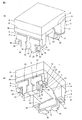
この発明に係るコイル部品の説明にあたり、コイル部品の一例としてのコモンモードチョークコイルを採り上げる。図1および図2を主として参照して、この発明の一実施形態によるコイル部品としてのコモンモードチョークコイル1について説明する。
In the description of the coil component according to the present invention, a common mode choke coil as an example of the coil component will be taken up. A common
コモンモードチョークコイル1は、巻芯部2を有するフェライトコア3を備えている。フェライトコア3は、ドラム状をなし、巻芯部2の互いに逆の第1および第2の端部にそれぞれ設けられた第1および第2の鍔部4および5を備えている。コモンモードチョークコイル1は、さらに、第1および第2の鍔部4および5間に渡された板状のフェライト板6を備えている。なお、フェライトコア3は、フェライト以外の材料からなるコアに置き換えられてもよい。
The common
フェライトコア3は、キュリー温度が150℃以上であることが好ましい。低温から150℃まで、インダクタンス値を一定以上に維持することができるためである。また、フェライトコア3の比透磁率が1500以下であることが好ましい。この構成によれば、フェライトコア3の構成や材料に高透磁率用の特殊なものを用いる必要が無い。したがって、フェライトコア3の設計自由度が向上し、たとえばキュリー温度が150℃以上であるようなフェライトコア3を容易に設計できる。このように、上記構成によれば、高温でのインダクタンス値が確保された、温度特性の良好なコモンモードチョークコイル1を提供できる。
The
なお、フェライト板6についても、キュリー温度が150℃以上であることが好ましく、また、比透磁率が1500以下であることが好ましい。
The
鍔部4および5は、それぞれ、巻芯部2側に向きかつ巻芯部2の各端部を位置させる内側端面7および8と、内側端面7および8の反対側の外側に向く外側端面9および10とを有する。また、鍔部4および5は、それぞれ、実装時において実装基板(図示しない。)側に向けられる下面11および12、ならびに下面11および12の反対側の上面13および14を有している。前述したフェライト板6は、鍔部4および5の上面13および14に接合されている。さらに、第1の鍔部4は、下面11と上面13とを連結する方向に延びかつ互いに逆の側方に向く第1および第2の側面15および16を有し、第2の鍔部5は、下面12と上面14とを連結する方向に延びかつ互いに逆の側方に向く第1および第2の側面17および18を有する。
The
また、第1の鍔部4における下面11の両端部に、切欠き形状の窪み19および20が設けられる。同様に、第2の鍔部5における下面12の両端部に、切欠き形状の窪み21および22が設けられる。
Further, notch-shaped
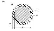
コモンモードチョークコイル1は、さらに、巻芯部2に螺旋状に巻回された第1および第2のワイヤ23および24を備えている。なお、図1および図2では、ワイヤ23および24の各々の端部のみが図示され、巻芯部2上でのワイヤ23および24の図示が省略されている。これらワイヤ23および24は、一方のワイヤ23について図3に図示するように、線状の中心導体25と、中心導体25の周面を覆う絶縁被覆層26とを有する。
The common
中心導体25は、たとえば銅線からなる。絶縁被覆層26は、好ましくは、たとえばポリアミドイミドや、イミド変成ポリウレタンのような少なくともイミド結合を含む樹脂からなる。この構成によれば、絶縁被覆層に対して、たとえば150℃においても分解しないといった耐熱性を与えることができる。したがって、150℃といった高温でも、線間容量が変化せず、Sdd11特性を良好なものとすることができる。また、150℃といった高温でもノイズ抑制効果に優れるといった効果の実効性を高めることができる。
The
第1および第2のワイヤ23および24は、互いに並行しながら同方向に巻回される。このとき、ワイヤ23および24は、いずれか一方が内層側に、いずれか他方が外層側に、というように、2層巻きにされても、巻芯部2の軸線方向において交互に配列されかつ互いに平行に並んだ状態で巻くバイファイラ巻きにされてもよい。
The first and
中心導体25の径Dは35μm以下であることが好ましい。この構成によれば、ワイヤ23および24の径を細くできるので、巻芯部2へのワイヤ23および24の巻き数を多くすることや、ワイヤ23および24の巻き数を変えずに小型化すること、ワイヤ23および24やコイル外形を変えずにワイヤ間隔を広げることなどができる。また、コイル外形に占めるワイヤ23および24の割合が減ることで、たとえばフェライトコア3などの他の部分の寸法を拡大できるため、特性をさらに向上できる。
The diameter D of the
また、中心導体25の径Dは28μm以上であることが好ましい。この構成によれば、中心導体25の断線を生じにくくすることができる。
Further, the diameter D of the
また、絶縁被覆層26の厚み寸法T4は6μm以下であることが好ましい。この構成によれば、ワイヤ23および24の径を細くできるので、巻芯部2へのワイヤ23および24の巻き数を多くすることや、ワイヤ23および24の巻き数を変えずに小型化すること、ワイヤ23および24やコイル外形を変えずにワイヤ間隔を広げることなどができる。また、コイル外形に占めるワイヤ23および24の割合が減ることで、たとえばフェライトコア3などの他の部分の寸法を拡大できるため、特性をさらに向上できる。
Further, the thickness dimension T4 of the insulating
また、絶縁被覆層26の厚み寸法T4は3μm以上であることが好ましい。この構成によれば、巻回状態で隣り合うワイヤ23および24の中心導体25間の距離を長くできるので、線間容量が小さくなり、そのため、Sdd11特性を良好なものとすることができる。
Further, the thickness dimension T4 of the insulating
コモンモードチョークコイル1は、さらに、第1ないし第4の端子電極27〜30を備えている。これら第1ないし第4の端子電極27〜30のうち、第1および第3の端子電極27および29は、第1および第2の側面15および16が対向する方向に配列されて、第1の鍔部4に接着剤を介して取り付けられる。第2および第4の端子電極28および30は、第1および第2の側面17および18が対向する方向に配列されて、第2の鍔部5に接着剤を介して取り付けられる。
The common
第1の端子電極27と第4の端子電極30とは、互いに同じ形状であり、第2の端子電極28と第3の端子電極29とは、互いに同じ形状である。また、第1の端子電極27と第3の端子電極29とは、互いに面対称形状をなし、第2の端子電極28と第4の端子電極30とは、互いに面対称形状をなしている。したがって、第1ないし第4の端子電極27〜30のうちのいずれか1つの端子電極、たとえば図1(A)および(B)において最も良好に図示されている第1の端子電極27について、その詳細を説明し、第2、第3および第4の端子電極28、29および30の詳細については、その説明を省略する。
The first
端子電極27は、通常、たとえばリン青銅やタフピッチ銅などの銅系合金からなる1枚の金属板に対して順送プレス加工を施すことにより製造される。端子電極27の材料となる金属板は、0.15mm以下の厚みを有しており、たとえば0.1mmの厚みである。
The
図1(B)によく示されているように、端子電極27は、鍔部4の外側端面9に沿って延びる基部31と、当該基部31から、鍔部4の外側端面9と下面11とが交差する稜線部分を覆う第1の屈曲部32を介して、鍔部4の下面11に沿って延びる実装部33と、を備えている。実装部33は、コモンモードチョークコイル1が図示しない実装基板上に実装されるとき、実装基板上の導電ランドに対して、はんだ付け等によって電気的かつ機械的に接続される部分となる。
As is well shown in FIG. 1 (B), the
さらに、図1(B)を参照して、端子電極27は、実装部33から第2の屈曲部34を介して延びる立上がり部35、および立上がり部35から第3の屈曲部36を介して延びる受け部37を備えている。上記立上がり部35は、窪み19を規定する垂直壁38に沿って延び、上記受け部37は、窪み19を規定する底面壁39に沿って延びている。受け部37は、ワイヤ23の端部に沿うとともに、ワイヤ23を端子電極27に電気的かつ機械的に接続する部分となる。受け部37は、ワイヤ23を受ける面として、図1(A)および(B)からわかるように、ワイヤ23の延びる方向に対して直交する方向において連続して延びる受け面を形成している。
Further, referring to FIG. 1 (B), the
なお、上述の受け部37は、鍔部4から所定の間隔を置いて位置していることが好ましい。より特定的には、立上がり部35および受け部37は、窪み19を規定する垂直壁38および底面壁39から所定の間隔を置いて位置していて、垂直壁38および底面壁39に接していないことが好ましい。
The above-mentioned receiving
上述した第1の端子電極27における基部、第1の屈曲部、実装部、第2の屈曲部、立上がり部、第3の屈曲部および受け部をそれぞれ指すために用いた参照符号31、32、33、34、35、36および37は、必要に応じて、第2、第3および第4の端子電極28、29および30における対応の基部、第1の屈曲部、実装部、第2の屈曲部、立上がり部、第3の屈曲部および受け部をそれぞれ指すためにも用いることにする。
前述した第1のワイヤ23の第1端は第1の端子電極27に電気的に接続され、第1のワイヤ23の第1端とは逆の第2端は第2の端子電極28に電気的に接続される。他方、第2のワイヤ24の第1端は第3の端子電極29に電気的に接続され、第2のワイヤ24の第1端とは逆の第2端は第4の端子電極30に電気的に接続される。
The first end of the
通常、上述したワイヤ23および24と端子電極27〜30との接続工程を実施する前に、ワイヤ23および24を巻芯部2上に巻回する工程が実施される。巻回工程では、フェライトコア3を巻芯部2の中心軸線まわりに回転させた状態で、ノズルからワイヤ23および24がトラバースされながら巻芯部2に向かって供給される。これによって、ワイヤ23および24が巻芯部2上で螺旋状に巻回される。
Usually, before carrying out the step of connecting the
この巻回工程において、フェライトコア3を上述のように回転させるため、フェライトコア3は、回転駆動源に接続されたチャックによって保持される。チャックは、フェライトコア3における一方の鍔部、たとえば第1の鍔部4を保持するように設計されている。
In this winding step, since the
第1の鍔部4の外側端面9に注目すると、そこには、上面13と外側端面9とが交差する稜線に沿って延びる凸状の段部40が形成されている。また、外側端面9における上記段部40が形成された領域より前記下面11に近い側の領域には平坦面41が形成されている。
Focusing on the
一方、フェライトコア3には、端子電極27〜30が既に取り付けられている。したがって、端子電極27の基部31および端子電極29の基部31は、第1および第2の側面15および16が対向する方向に互いに隣接しながら、外側端面9における上記平坦面41に沿って位置している。これら端子電極27の基部31と端子電極29の基部31との間の間隔については、図2(C)に示すように、下面11により近い側での間隔S1が、上面13(あるいは段部40)により近い側での間隔S2より広くなっている。この実施形態では、2つの基部31が、ともにT字状とされることによって、上述のようなS1>S2となる間隔を実現している。
On the other hand,
チャックのつかみ部は、鍔部4における(1)第1の側面15、(2)第2の側面16、(3)上面13、(4)段部40に加えて、(5)平坦面41の上記間隔S1で規定される部分、といった5つの異なる部分に接触した状態でフェライトコア3を保持する。したがって、ワイヤ23および24の巻回工程において、回転されるフェライトコア3の姿勢を安定させることができる。
The grip portion of the chuck is (1) a
端子電極27の基部31と端子電極29の基部31との間隔について、下面11により近い側での間隔S1は、0.3mmより広いことが好ましい。これによって、チャックのつかみ部を平坦面41に当接させるのに十分な面積を確保することができる。また、上面13により近い側での間隔S2は、0.1mm以上かつ0.3mm以下であることが好ましい。通常、順送プレス加工を施す場合、ワークとしての金属板の厚み寸法より小さい寸法で打抜きを行なうことが困難である。したがって、前述したように、端子電極27〜30の材料となる金属板の厚み寸法を0.1mmとしたとき、間隔S2を0.1mm以上かつ0.3mm以下とすることにより、順送プレス加工を容易に実施することができる。
Regarding the distance between the base 31 of the
上述のように、回転駆動源に接続されたチャックによって保持されたフェライトコア3を巻芯部2の中心軸線まわりに回転させることによって、ノズルから供給されたワイヤ23および24がトラバースされながら巻芯部2上で螺旋状に巻回される。巻芯部2上における第1および第2のワイヤ23および24の各々の巻き数は42ターン以下であることが好ましい。ワイヤ23および24の総長さを短くすることができるので、Sdd11特性をより良好なものとすることができるためである。なお、インダクタンス値の確保のためには、ワイヤ23および24の各々の巻き数は39ターン以上であることが好ましい。
As described above, by rotating the
なお、巻回工程において、チャックは、一方の鍔部、たとえば第1の鍔部4のみをつかむように設計されているので、他方の鍔部、たとえば第2の鍔部5については、第1の鍔部4において採用された、段部40および平坦面41を有する構成は採用されなくてもよい。また、第2および第4の端子電極28および30についても、前述したような第1および第3の端子電極27および29において採用された、基部31の形状および配置は採用されなくてもよい。
In the winding process, the chuck is designed to grip only one flange portion, for example, the
しかしながら、上述したような特徴的構成が、第1および第2の鍔部4および5の双方に採用され、かつ、第1ないし第4の端子電極27〜30のすべてに採用されると、巻回工程において、フェライトコア3の方向性をなくすことができ、チャックによるつかみ工程での方向ミスをなくすことができる。
However, when the characteristic configuration as described above is adopted for both the first and
上述の巻回工程を終えた後、以下に説明するワイヤ23および24と端子電極27〜30との接続工程が実施される。
After completing the winding step described above, the connecting steps of the
以下、代表して、第1のワイヤ23を第1の端子電極27に接続する工程について図4を参照して説明する。図4には、第1の端子電極27の受け部37および第1のワイヤ23の端部が模式的に図示されている。
Hereinafter, the process of connecting the
前述の巻回工程を終えた段階では、ワイヤ23の端部は、図4(1)に示すように、受け部37および受け部37の先端にある先端部37a上にまで引き出された状態となっている。また、ワイヤ23の端部は、その全周において、絶縁被覆層26が除去された状態とされる。絶縁被覆層26の除去には、たとえばレーザ光照射が適用される。
At the stage where the above-mentioned winding step is completed, as shown in FIG. 4 (1), the end portion of the
次に、同じく図4(1)に示すように、溶接のためのレーザ光42が、ワイヤ23における絶縁被覆層26から露出した中心導体25と受け部37の先端部37aとが重なった領域に向かって照射される。このとき、レーザ光42は、受け部37における、ワイヤ23の中心導体25が配置された側から照射されるので、当該受け部37における、ワイヤ23の中心導体25が配置される側は、開放されていなければならない。これによって、中心導体25およびそれを受ける先端部37aが溶融する。このとき、図4(2)に示すように、溶融した中心導体25および先端部37aは、そこに作用する表面張力によって玉状となり、溶接塊部43が形成される。受け部37と溶接塊部43とは、受け部37の形態の一部を残したまま、溶接され合っていて、溶接塊部43は、受け部37上に位置している。すなわち、溶接塊部43は、中心導体25および端子電極27の受け部37(先端部37a)が一体化したものであり、中心導体25は、その先端が溶接塊部43から露出しない状態で、溶接塊部43の中に取り込まれる。
Next, as also shown in FIG. 4 (1), the
前述したように、好ましくは、受け部37は、鍔部4から所定の間隔を置いて位置していて、鍔部4に接していないようにされる。この構成は必須ではないが、この構成によれば、上述した溶接工程において、受け部37での温度上昇が鍔部4側に伝わりにくくなり、熱によるフェライトコア3への悪影響を低減することができる。
As described above, preferably, the receiving
図5には、コモンモードチョークコイルの実際の製品におけるワイヤと端子電極との電気的接続部分を正面方向から撮影した写真が示されている。図5において、右上の丸い部分が溶融玉、すなわち溶接塊部43に相当している。図6には、図5に示したワイヤと端子電極との電気的接続部分の断面を拡大して撮影した写真が示されている。図7は、図6に示した写真をトレースして作成したもので、図6の写真の説明図である。なお、前述の図4は、レーザ光42を上から下に向かって照射するように図示されたため、図5ないし図7における天地関係と逆になっている。
FIG. 5 shows a photograph of the electrical connection portion between the wire and the terminal electrode in an actual product of the common mode choke coil taken from the front direction. In FIG. 5, the round portion on the upper right corresponds to the molten ball, that is, the welded
図6と図7とを対照ながら説明すると、溶接工程により、先端部37aだけでなく、溶接後において残存している受け部37と溶接塊部43とは溶接され合い、互いに接触している。ワイヤ23の中心導体25は、受け部37と溶接塊部43との間に位置し、溶接塊部43に内包されている。また、絶縁被覆層26がワイヤ23の端部の全周において除去されることで、ワイヤ23の端部では、ワイヤ23の中心導体25についても、受け部37および溶接塊部43と溶接され合っていることが好ましい。さらに、好ましくは、溶接塊部43の中には、絶縁被覆層26に由来する物質が存在していない。なお、受け部37と溶接塊部43との区別については、外縁形状が板状のままである部分を受け部37、外縁形状が曲面状となっている部分を溶接塊部43とすることができる。
Explaining with reference to FIGS. 6 and 7, not only the
このようにして、強固な溶接が達成される。また、ワイヤ23の中心導体25は、受け部37と溶接塊部43との間に位置し、その全周が溶接塊部43に内包されるので、より高い機械的強度、より低い電気抵抗、より高い耐ストレス性、より高い化学的な耐浸食性等が得られ、溶接構造に対するより高い信頼性が実現される。また、溶接塊部43の中に絶縁被覆層26に由来する物質が存在しないので、溶融時のブローホールを低減させることができ、この点においても、信頼性の高い溶接構造を得ることができる。また、前述したレーザ光42の照射を可能にするため、受け部37における、ワイヤ23の中心導体25が配置される側は、開放されている。
In this way, strong welding is achieved. Further, the
以上、第1の端子電極27と第1のワイヤ23との接続について説明したが、他の端子電極28〜30とワイヤ23または24との接続についても同様の工程が実施される。
Although the connection between the first
上述したワイヤ23および24の巻回工程、ならびにワイヤ23および24の端子電極27〜30への接続工程を終えた後、フェライト板6が第1および第2の鍔部4および5の各々の上面13および14に接着剤を介して接合される。このようにして、フェライトコア3とフェライト板6とによって閉磁路が形成されるので、インダクタンス値を向上させることができる。
After completing the winding steps of the
なお、フェライト板6は、磁路を形成できる磁性樹脂板または金属板に置き換えられてもよい。あるいは、フェライト板6は、コモンモードチョークコイル1において省略されてもよい。
The
上述のようにして完成されたコモンモードチョークコイル1において熱膨張および収縮等によるストレスを受けた場合、あるいはコモンモードチョークコイル1の製造途中においてワイヤ23および24が引き回された場合、ワイヤ23および24の少なくとも一方が端子電極27〜30の少なくとも1つに接触している箇所において、絶縁被覆層26が損傷したり、中心導体25が断線したりすることがある。特に、コモンモードチョークコイル1が車載用に向けられるとき、熱膨張および収縮等によるストレスをより受けやすい。なお、このような接触箇所は、たとえば、図2(B)において円で囲んだ箇所Cに見出すことができる。
When the common
上述の状況を、ワイヤ23および24と端子電極27〜30とを代表して、図8に示した第1のワイヤ23と第1の端子電極27とに関連して説明する。
The above situation will be described in relation to the
前述したように、端子電極27は、たとえばリン青銅やタフピッチ銅などの銅系合金からなる1枚の金属板に対して順送プレス加工を施すことにより製造される。端子電極27の材料となる金属板は、0.15mm以下の厚みを有しており、たとえば0.1mmの厚みである。このような場合、プレス加工後の端子電極27において、そのエッジ部分44には、プレスによるせん断の結果、鋭利な「ダレ」または「バリ」が生じやすい。したがって、鋭利な「ダレ」または「バリ」が生じたエッジ部分44に、図8(B)に示すように、ワイヤ23が接触すると、前述したような絶縁被覆層26の損傷や中心導体25の断線が生じることがある。
As described above, the
そこで、この実施形態では、図8(A)に示すように、上述のエッジ部分44において面取りが施されている。このように面取りをエッジ部分44に施すことにより、ワイヤ23が端子電極27に接触しても、接触面積の拡大や接触箇所の複数化により、端子電極27からワイヤ23に及ぼされる荷重が分散される。したがって、前述した絶縁被覆層26の損傷や中心導体25の断線を生じにくくすることができる。その結果、ワイヤ23におけるエッジ部分44に接触する部分では、中心導体25が絶縁被覆層26で適正に覆われている状態とすることができる。
Therefore, in this embodiment, as shown in FIG. 8A, the above-mentioned
上述したように面取りが施されたエッジ部分44を備える端子電極27は、好ましくは、プレス加工に含まれる複数の工程の中に、コイニング工程を挿入することによって得られる。
The
図9を参照して、より具体的に説明すると、まず、(1)に示すように、端子電極27の材料となる金属板45が用意される。次に、(2)に示すように、コイニング金型46が金属板45に向かって圧入され、金属板45の一方主面側に型模様が付与される。コイニング金型46に凸状アール面47が形成されていると、金属板45側に対応の凹状アール面48を有する型模様が付与される。次に、(3)に示すように、パンチ49とダイ50とを用いて、金属板45に対してせん断に基づく板抜き加工が施され、コイニング金型46による圧入領域より内側の位置で金属板45が切断され、端子電極27が得られる。
More specifically, with reference to FIG. 9, first, as shown in (1), a
得られた端子電極27のエッジ部分44には、上述のコイニング金型46による凸状アール面47に対応する凹状アール面48を形成した面取り部が残される。このように、凹状アール面48を形成したエッジ部分44によれば、2点においてワイヤ23に接触することになる。すなわち、エッジ部分44におけるワイヤ23に接触する2点に挟まれた領域は、凹面をなしているためである。
On the
図8(A)に示した端子電極27のエッジ部分44には、凹状アール面48を形成した面取りが施されていたが、その変形例として、たとえば図10に示すように、断面V字状凹面51を形成した面取りが施されてもよい。この場合であっても、エッジ部分44におけるワイヤ23に接触する2点に挟まれた領域は、凹面をなしている。そして、エッジ部分44は、2点においてワイヤ23に接触することになり、ワイヤ23に及ぼされる損傷を低減することができる。
The
面取りの他の変形例として、たとえば図11に示すように、2個の断面V字状凹面51を形成した面取りが施されてもよい。この変形例によれば、図10に示した変形例の場合よりも、ワイヤ23に接触する箇所を増やすことができ、ワイヤ23に及ぼされる損傷をより低減することができる。なお、ワイヤ23に接触する箇所は、断面V字状凹面の数に応じて、さらに増やすこともできる。
As another modification of chamfering, for example, as shown in FIG. 11, chamfering may be performed in which two V-shaped
面取りの形状については、さらに他の変形例が多数あり得る。たとえば、上述の断面V字状凹面のV字の屈曲部のみを曲面とした形状、面取りの底面が端子電極を構成する金属板の主面と平行でない形状、などに変更することができる。また、ワイヤと端子電極を構成する金属板との接触面積をより大きくするように、たとえば凸状アール面のような形状に変更されてもよい。 There may be many other variations on the chamfer shape. For example, it can be changed to a shape in which only the V-shaped bent portion of the V-shaped concave surface having a cross section is curved, or a shape in which the bottom surface of the chamfer is not parallel to the main surface of the metal plate constituting the terminal electrode. Further, the shape may be changed to, for example, a convex rounded surface so as to increase the contact area between the wire and the metal plate constituting the terminal electrode.
上述したような面取りの形状は、図9(2)に示したコイニング金型46に相当する金型の形状を変更することにより、容易に変更することができる。ただし、面取りを施す方法は、上記のコイニング工程の挿入に限られず、同様の構造を得られるのであれば、方法に制限はない。
The shape of the chamfer as described above can be easily changed by changing the shape of the mold corresponding to the coining
なお、ワイヤ23が端子電極27のエッジ部分44に接触する箇所として、図2(B)において円で囲んだ箇所Cを例示したが、同様の接触状態を、ワイヤ23および24の引き回し経路に関連して、他の箇所にも見出すことができる。一方で、端子電極27のうち、ワイヤ23が接触しない部分には面取りを施す必要は無い。
As a portion where the
図2(B)に示すように、フェライトコア3の外形寸法に関して、コモンモードチョークコイル1の小型化を図るため、巻芯部2の軸線方向に測定した外形寸法L1は3.4mm以下であり、巻芯部2の軸線方向に直交する方向に測定した外形寸法L2は2.7mm以下であることが好ましい。この構成によれば、コモンモードチョークコイル1の小型化を図ることで、低EMC部品に対してコモンモードチョークコイル1をより近くに配置でき、実質的なノイズ低減効果を向上することができる。また、フェライトコア3の体積が一定以下であることで、加熱冷却によるフェライトコア3の膨張収縮の絶対量を低減でき、低温から高温までの特性変動を低減できる。
As shown in FIG. 2B, with respect to the external dimensions of the
また、図2(A)に示すように、巻芯部2の軸線方向に測定した第1および第2の鍔部の各々の厚み寸法T1およびT2は0.7mm未満であることが好ましい。この構成によれば、コモンモードチョークコイル1の限られた外形寸法L1およびL2の範囲内で、巻芯部2の軸線方向の長さを長くすることができる。このことは、ワイヤ23および24の巻き態様についての自由度が上がることを意味する。そのため、ワイヤ23および24の巻き数を多くでき、その結果、インダクタンス値を高めることができ、あるいは、巻回されるワイヤ23および24をより太くすることができ、その結果、ワイヤ23および24の断線を生じにくくするとともに、ワイヤ23および24が有する直流抵抗を減じることができる。また、ワイヤ間隔(絶縁被膜厚)を広げることでワイヤ間容量を低減することができる。
Further, as shown in FIG. 2A, the thickness dimensions T1 and T2 of the first and second flange portions measured in the axial direction of the winding
また、コモンモードチョークコイル1が実装面上に実装された状態において、第1および第2の鍔部4および5の各々の、実装面に投影した面積、すなわち、図2(B)に現れた鍔部4および5の各々の面積は、1.75mm2未満であることが好ましい。この構成によれば、上述の場合と同様、コモンモードチョークコイル1の限られた外形寸法L1およびL2の範囲内で、巻芯部2の軸線方向の長さを長くすることができ、そのため、上述の場合と同様の効果が期待できる。
Further, in a state where the common
また、巻芯部2の断面積は1.0mm2未満であることが好ましい。この構成によれば、ワイヤ23および24の巻き数を維持しながら、ワイヤ23および24の総長さを短くすることができるので、Sdd11特性の向上を図ることができる。
Further, the cross-sectional area of the winding
また、コモンモードチョークコイル1が実装面上に実装された状態において、巻芯部2と実装面との間の距離、すなわち、図2(A)に示した距離L3は、0.5mm以上であることが好ましい。この構成によれば、実装面側に存在し得るグラウンドパターンと、巻芯部2上に巻回されたワイヤ23および24と、の間の距離を長くすることができるので、グラウンドパターンとワイヤワイヤ23および24との間に形成される浮遊容量を減じることができ、そのため、モード変換特性をより良好なものとすることができる。
Further, when the common
また、図2(A)に示すように、フェライト板6の厚み寸法T3は0.75mm以下であることが好ましい。この構成によれば、コモンモードチョークコイル1の総高さ寸法を小さくすることができる。あるいは、コモンモードチョークコイル1の総高さ寸法を大きくすることなく、巻芯部2の高さ位置を実装面から離してより高くすることができる。その結果、実装面側に存在するグラウンドパターンとワイヤ23および24との間に形成される浮遊容量を減じることができ、そのため、モード変換特性をより良好なものとすることができる。
Further, as shown in FIG. 2A, the thickness dimension T3 of the
また、第1および第2の鍔部4および5とフェライト板6との間の隙間は10μm以下であることが好ましい。この構成によれば、フェライトコア3とフェライト板6とによって形成される磁路の磁気抵抗を低くすることができるので、インダクタンス値を高くすることができる。ここで、第1および第2の鍔部4および5とフェライト板6との間の隙間は、たとえば、一方の鍔部4または5の端面に平行な面が現れるように、コモンモードチョークコイル1を研磨した試料について、上記隙間の寸法をたとえば幅方向(図2(B)におけるL2が示す方向)に均等間隔で設定された5箇所で測定し、それら測定値を算術平均することにより求めることができる。
Further, the gap between the first and
以上のように説明したコモンモードチョークコイル1は、150℃でのコモンモードインダクタンス値が100kHzにおいて160μH以上であり、かつ20℃でのリターンロスが10MHzにおいて−27.1dB以下であるといった構成を備えることを特徴としている。コモンモードインダクタンス値が160μH以上であると、BroadR-Reachなどの高速通信で求められるノイズ除去性能である、コモンモード除去比−45dB以下を満足することができる。また、上記高速通信では、コモンモードチョークコイル1における通信信号の通過特性を向上させ、通信品質を確保している。特に、リターンロスが−27dB以下であれば、問題なく通信が実現できる。よって、リターンロスが−27.1dB以下であると、より高品質な高速通信を実現できる。したがって、コモンモードチョークコイル1によれば、より高温で高速通信を最低限使用可能としつつ、常温ではより高品質な高速通信を実現できる。
The common
また、コモンモードチョークコイル1は、好ましくは、130℃でのリターンロスが10MHzにおいて−27dB以下である。この構成によれば、より広い温度範囲で問題なく通信を実現するためのコモンモードチョークコイル1を提供できる。
Further, the common
以上、この発明に係るコイル部品を、より具体的なコモンモードチョークコイルに関する実施形態に基づいて説明したが、この実施形態は、例示的なものであり、その他種々の変形例が可能である。 The coil components according to the present invention have been described above based on a more specific embodiment relating to a common mode choke coil, but this embodiment is an example, and various other modifications are possible.
たとえば、コイル部品に備えるワイヤの本数およびワイヤの巻回方向、ならびに端子電極の個数等は、コイル部品の機能に応じて変更され得る。 For example, the number of wires provided in the coil component, the winding direction of the wires, the number of terminal electrodes, and the like can be changed according to the function of the coil component.
また、上記実施形態では、端子電極とワイヤとの接続のため、レーザ溶接を用いたが、これに限られず、アーク溶接などを用いてもよい。 Further, in the above embodiment, laser welding is used for connecting the terminal electrode and the wire, but the present invention is not limited to this, and arc welding or the like may be used.
また、この発明に係るコイル部品は、コアを備えないものであってもよい。 Further, the coil component according to the present invention may not include a core.
1 コモンモードチョークコイル(コイル部品)
2 巻芯部
3 フェライトコア
4,5 鍔部
23,24 ワイヤ
25 中心導体
26 絶縁被覆層
27〜30 端子電極
37 受け部
42 レーザ光
43 溶接塊部
1 Common mode choke coil (coil parts)
2
Claims (5)
前記ワイヤの端部において前記中心導体と電気的に接続される複数の端子電極と、
を備え、
前記端子電極は、前記ワイヤの端部に沿って延び、前記ワイヤの先端側に先端部を位置させている受け部を有し、
前記受け部は、前記ワイヤの延びる方向に対して直交する方向において連続して延びる受け面を形成しており、
前記絶縁樹脂層は、イミド結合を含む樹脂からなり、
前記ワイヤの端部は、その全周において、前記絶縁被覆層が除去されていて、
前記ワイヤの端部には、前記中心導体と前記受け部とが一体化した溶接塊部が形成され、前記溶接塊部の中に前記絶縁被覆層に由来する物質が存在せず、
前記受け部と前記溶接塊部とは、前記受け部の形態の一部を残したまま、溶接され合っていて、前記溶接塊部は、前記受け部の前記受け面上に位置しており、
前記ワイヤの前記中心導体は、その先端が前記溶接塊部から露出しない状態で、前記溶接塊部の中に取り込まれている、
コイル部品。 A wire having a linear central conductor and an insulating coating layer covering the peripheral surface of the central conductor,
A plurality of terminal electrodes electrically connected to the center conductor at the end of the wire,
With
The terminal electrode has a receiving portion that extends along the end of the wire and positions the tip on the tip side of the wire.
The receiving portion forms a receiving surface that extends continuously in a direction orthogonal to the extending direction of the wire.
The insulating resin layer is made of a resin containing an imide bond.
The insulating coating layer is removed from the end of the wire all around the wire.
At the end of the wire, a welded ingot in which the central conductor and the receiving portion are integrated is formed, and the substance derived from the insulating coating layer does not exist in the welded ingot.
The receiving portion and the welded ingot are welded to each other while leaving a part of the form of the receiving portion, and the welded ingot is located on the receiving surface of the receiving portion.
The central conductor of the wire is incorporated into the weld block portion in a state where the tip thereof is not exposed from the weld block portion.
Coil parts.
前記ワイヤは、前記巻芯部上に螺旋状に巻回され、
前記端子電極は、前記鍔部に取り付けられている、
請求項1ないし3のいずれかに記載のコイル部品。 Further provided with a core portion and a core having a flange portion provided at an end portion of the winding core portion.
The wire is spirally wound on the winding core portion.
The terminal electrode is attached to the collar portion,
The coil component according to any one of claims 1 to 3.
Priority Applications (5)
| Application Number | Priority Date | Filing Date | Title |
|---|---|---|---|
| JP2017042938A JP6884603B2 (en) | 2017-03-07 | 2017-03-07 | Coil parts |
| US15/886,385 US10720273B2 (en) | 2017-03-07 | 2018-02-01 | Coil component |
| DE102018202790.0A DE102018202790A1 (en) | 2017-03-07 | 2018-02-23 | coil component |
| CN201810182379.0A CN108573794A (en) | 2017-03-07 | 2018-03-06 | Coil component |
| CN201820307800.1U CN208111215U (en) | 2017-03-07 | 2018-03-06 | Coil component |
Applications Claiming Priority (1)
| Application Number | Priority Date | Filing Date | Title |
|---|---|---|---|
| JP2017042938A JP6884603B2 (en) | 2017-03-07 | 2017-03-07 | Coil parts |
Publications (2)
| Publication Number | Publication Date |
|---|---|
| JP2018148079A JP2018148079A (en) | 2018-09-20 |
| JP6884603B2 true JP6884603B2 (en) | 2021-06-09 |
Family
ID=63258776
Family Applications (1)
| Application Number | Title | Priority Date | Filing Date |
|---|---|---|---|
| JP2017042938A Active JP6884603B2 (en) | 2017-03-07 | 2017-03-07 | Coil parts |
Country Status (4)
| Country | Link |
|---|---|
| US (1) | US10720273B2 (en) |
| JP (1) | JP6884603B2 (en) |
| CN (2) | CN208111215U (en) |
| DE (1) | DE102018202790A1 (en) |
Families Citing this family (8)
| Publication number | Priority date | Publication date | Assignee | Title |
|---|---|---|---|---|
| US9899131B2 (en) * | 2015-07-20 | 2018-02-20 | Cyntec Co., Ltd. | Structure of an electronic component and an inductor |
| JP6884603B2 (en) * | 2017-03-07 | 2021-06-09 | 株式会社村田製作所 | Coil parts |
| JP7286936B2 (en) * | 2018-10-05 | 2023-06-06 | Tdk株式会社 | Coil devices, pulse transformers and electronic components |
| JP7059953B2 (en) * | 2019-02-07 | 2022-04-26 | 株式会社村田製作所 | Manufacturing method of coil parts |
| JP7336855B2 (en) | 2019-02-28 | 2023-09-01 | 太陽誘電株式会社 | Coil parts and electronic equipment |
| JP7213447B2 (en) * | 2019-09-25 | 2023-01-27 | 株式会社豊田自動織機 | Automotive electric compressor |
| JP7450316B2 (en) | 2020-01-31 | 2024-03-15 | 株式会社タムラ製作所 | reactor |
| JP7363582B2 (en) * | 2020-03-03 | 2023-10-18 | Tdk株式会社 | Coil parts and their manufacturing method |
Family Cites Families (8)
| Publication number | Priority date | Publication date | Assignee | Title |
|---|---|---|---|---|
| JP4311575B2 (en) * | 2005-10-03 | 2009-08-12 | 東京パーツ工業株式会社 | Wire wound chip type common mode choke coil |
| JP4184394B2 (en) | 2006-06-30 | 2008-11-19 | Tdk株式会社 | Coil component and method for manufacturing coil component |
| JP5262396B2 (en) * | 2008-07-28 | 2013-08-14 | パナソニック株式会社 | Electronic components |
| JP5786660B2 (en) * | 2011-11-08 | 2015-09-30 | スミダコーポレーション株式会社 | Magnetic component and method of manufacturing magnetic component |
| JP5699949B2 (en) * | 2012-01-23 | 2015-04-15 | Tdk株式会社 | Coil parts manufacturing method and wire connecting method |
| JP5652413B2 (en) * | 2012-02-17 | 2015-01-14 | Tdk株式会社 | Coil parts manufacturing method and wire connecting method |
| JP6468424B2 (en) * | 2015-01-22 | 2019-02-13 | Tdk株式会社 | Coil device |
| JP6884603B2 (en) * | 2017-03-07 | 2021-06-09 | 株式会社村田製作所 | Coil parts |
-
2017
- 2017-03-07 JP JP2017042938A patent/JP6884603B2/en active Active
-
2018
- 2018-02-01 US US15/886,385 patent/US10720273B2/en active Active
- 2018-02-23 DE DE102018202790.0A patent/DE102018202790A1/en active Pending
- 2018-03-06 CN CN201820307800.1U patent/CN208111215U/en active Active
- 2018-03-06 CN CN201810182379.0A patent/CN108573794A/en active Pending
Also Published As
| Publication number | Publication date |
|---|---|
| CN208111215U (en) | 2018-11-16 |
| US10720273B2 (en) | 2020-07-21 |
| US20180261365A1 (en) | 2018-09-13 |
| DE102018202790A1 (en) | 2018-09-13 |
| JP2018148079A (en) | 2018-09-20 |
| CN108573794A (en) | 2018-09-25 |
Similar Documents
| Publication | Publication Date | Title |
|---|---|---|
| JP6884603B2 (en) | Coil parts | |
| JP6865605B2 (en) | Common mode choke coil | |
| JP6766697B2 (en) | Coil parts | |
| JP6733580B2 (en) | Coil parts | |
| JP4184395B2 (en) | Coil component and method for manufacturing coil component | |
| JP4184394B2 (en) | Coil component and method for manufacturing coil component | |
| US10262787B2 (en) | Coil component | |
| US11024459B2 (en) | Method of manufacturing coil component | |
| JP7059953B2 (en) | Manufacturing method of coil parts | |
| US11798732B2 (en) | Coil component manufacturing method | |
| JP6658682B2 (en) | Coil parts | |
| WO2019004038A1 (en) | Inductor component and method for manufacturing same | |
| JP6992101B2 (en) | Coil parts | |
| JP6844724B2 (en) | Coil parts | |
| JP7245062B2 (en) | COIL COMPONENT, ELECTRONIC DEVICE, AND COIL COMPONENT MANUFACTURING METHOD | |
| JP7336855B2 (en) | Coil parts and electronic equipment |
Legal Events
| Date | Code | Title | Description |
|---|---|---|---|
| A621 | Written request for application examination |
Free format text: JAPANESE INTERMEDIATE CODE: A621 Effective date: 20181009 |
|
| A131 | Notification of reasons for refusal |
Free format text: JAPANESE INTERMEDIATE CODE: A131 Effective date: 20190521 |
|
| A977 | Report on retrieval |
Free format text: JAPANESE INTERMEDIATE CODE: A971007 Effective date: 20190523 |
|
| A521 | Request for written amendment filed |
Free format text: JAPANESE INTERMEDIATE CODE: A523 Effective date: 20190710 |
|
| A131 | Notification of reasons for refusal |
Free format text: JAPANESE INTERMEDIATE CODE: A131 Effective date: 20191029 |
|
| A521 | Request for written amendment filed |
Free format text: JAPANESE INTERMEDIATE CODE: A523 Effective date: 20191224 |
|
| A02 | Decision of refusal |
Free format text: JAPANESE INTERMEDIATE CODE: A02 Effective date: 20200428 |
|
| A521 | Request for written amendment filed |
Free format text: JAPANESE INTERMEDIATE CODE: A523 Effective date: 20200715 |
|
| C60 | Trial request (containing other claim documents, opposition documents) |
Free format text: JAPANESE INTERMEDIATE CODE: C60 Effective date: 20200715 |
|
| A911 | Transfer to examiner for re-examination before appeal (zenchi) |
Free format text: JAPANESE INTERMEDIATE CODE: A911 Effective date: 20200727 |
|
| C21 | Notice of transfer of a case for reconsideration by examiners before appeal proceedings |
Free format text: JAPANESE INTERMEDIATE CODE: C21 Effective date: 20200728 |
|
| A912 | Re-examination (zenchi) completed and case transferred to appeal board |
Free format text: JAPANESE INTERMEDIATE CODE: A912 Effective date: 20201002 |
|
| C211 | Notice of termination of reconsideration by examiners before appeal proceedings |
Free format text: JAPANESE INTERMEDIATE CODE: C211 Effective date: 20201006 |
|
| C22 | Notice of designation (change) of administrative judge |
Free format text: JAPANESE INTERMEDIATE CODE: C22 Effective date: 20201215 |
|
| C13 | Notice of reasons for refusal |
Free format text: JAPANESE INTERMEDIATE CODE: C13 Effective date: 20210112 |
|
| A521 | Request for written amendment filed |
Free format text: JAPANESE INTERMEDIATE CODE: A523 Effective date: 20210224 |
|
| C23 | Notice of termination of proceedings |
Free format text: JAPANESE INTERMEDIATE CODE: C23 Effective date: 20210406 |
|
| C03 | Trial/appeal decision taken |
Free format text: JAPANESE INTERMEDIATE CODE: C03 Effective date: 20210511 |
|
| C30A | Notification sent |
Free format text: JAPANESE INTERMEDIATE CODE: C3012 Effective date: 20210511 |
|
| A61 | First payment of annual fees (during grant procedure) |
Free format text: JAPANESE INTERMEDIATE CODE: A61 Effective date: 20210512 |
|
| R150 | Certificate of patent or registration of utility model |
Ref document number: 6884603 Country of ref document: JP Free format text: JAPANESE INTERMEDIATE CODE: R150 |