JP6879236B2 - Method for manufacturing silicon carbide single crystal - Google Patents
Method for manufacturing silicon carbide single crystal Download PDFInfo
- Publication number
- JP6879236B2 JP6879236B2 JP2018045227A JP2018045227A JP6879236B2 JP 6879236 B2 JP6879236 B2 JP 6879236B2 JP 2018045227 A JP2018045227 A JP 2018045227A JP 2018045227 A JP2018045227 A JP 2018045227A JP 6879236 B2 JP6879236 B2 JP 6879236B2
- Authority
- JP
- Japan
- Prior art keywords
- crystal substrate
- seed crystal
- silicon carbide
- center
- single crystal
- Prior art date
- Legal status (The legal status is an assumption and is not a legal conclusion. Google has not performed a legal analysis and makes no representation as to the accuracy of the status listed.)
- Active
Links
Images


Classifications
-
- C—CHEMISTRY; METALLURGY
- C30—CRYSTAL GROWTH
- C30B—SINGLE-CRYSTAL GROWTH; UNIDIRECTIONAL SOLIDIFICATION OF EUTECTIC MATERIAL OR UNIDIRECTIONAL DEMIXING OF EUTECTOID MATERIAL; REFINING BY ZONE-MELTING OF MATERIAL; PRODUCTION OF A HOMOGENEOUS POLYCRYSTALLINE MATERIAL WITH DEFINED STRUCTURE; SINGLE CRYSTALS OR HOMOGENEOUS POLYCRYSTALLINE MATERIAL WITH DEFINED STRUCTURE; AFTER-TREATMENT OF SINGLE CRYSTALS OR A HOMOGENEOUS POLYCRYSTALLINE MATERIAL WITH DEFINED STRUCTURE; APPARATUS THEREFOR
- C30B23/00—Single-crystal growth by condensing evaporated or sublimed materials
- C30B23/02—Epitaxial-layer growth
- C30B23/06—Heating of the deposition chamber, the substrate or the materials to be evaporated
- C30B23/063—Heating of the substrate
-
- C—CHEMISTRY; METALLURGY
- C30—CRYSTAL GROWTH
- C30B—SINGLE-CRYSTAL GROWTH; UNIDIRECTIONAL SOLIDIFICATION OF EUTECTIC MATERIAL OR UNIDIRECTIONAL DEMIXING OF EUTECTOID MATERIAL; REFINING BY ZONE-MELTING OF MATERIAL; PRODUCTION OF A HOMOGENEOUS POLYCRYSTALLINE MATERIAL WITH DEFINED STRUCTURE; SINGLE CRYSTALS OR HOMOGENEOUS POLYCRYSTALLINE MATERIAL WITH DEFINED STRUCTURE; AFTER-TREATMENT OF SINGLE CRYSTALS OR A HOMOGENEOUS POLYCRYSTALLINE MATERIAL WITH DEFINED STRUCTURE; APPARATUS THEREFOR
- C30B23/00—Single-crystal growth by condensing evaporated or sublimed materials
- C30B23/002—Controlling or regulating
-
- C—CHEMISTRY; METALLURGY
- C30—CRYSTAL GROWTH
- C30B—SINGLE-CRYSTAL GROWTH; UNIDIRECTIONAL SOLIDIFICATION OF EUTECTIC MATERIAL OR UNIDIRECTIONAL DEMIXING OF EUTECTOID MATERIAL; REFINING BY ZONE-MELTING OF MATERIAL; PRODUCTION OF A HOMOGENEOUS POLYCRYSTALLINE MATERIAL WITH DEFINED STRUCTURE; SINGLE CRYSTALS OR HOMOGENEOUS POLYCRYSTALLINE MATERIAL WITH DEFINED STRUCTURE; AFTER-TREATMENT OF SINGLE CRYSTALS OR A HOMOGENEOUS POLYCRYSTALLINE MATERIAL WITH DEFINED STRUCTURE; APPARATUS THEREFOR
- C30B23/00—Single-crystal growth by condensing evaporated or sublimed materials
- C30B23/02—Epitaxial-layer growth
- C30B23/025—Epitaxial-layer growth characterised by the substrate
-
- C—CHEMISTRY; METALLURGY
- C30—CRYSTAL GROWTH
- C30B—SINGLE-CRYSTAL GROWTH; UNIDIRECTIONAL SOLIDIFICATION OF EUTECTIC MATERIAL OR UNIDIRECTIONAL DEMIXING OF EUTECTOID MATERIAL; REFINING BY ZONE-MELTING OF MATERIAL; PRODUCTION OF A HOMOGENEOUS POLYCRYSTALLINE MATERIAL WITH DEFINED STRUCTURE; SINGLE CRYSTALS OR HOMOGENEOUS POLYCRYSTALLINE MATERIAL WITH DEFINED STRUCTURE; AFTER-TREATMENT OF SINGLE CRYSTALS OR A HOMOGENEOUS POLYCRYSTALLINE MATERIAL WITH DEFINED STRUCTURE; APPARATUS THEREFOR
- C30B29/00—Single crystals or homogeneous polycrystalline material with defined structure characterised by the material or by their shape
- C30B29/10—Inorganic compounds or compositions
- C30B29/36—Carbides
Description
本発明は、昇華法によって炭化珪素の単結晶成長を行う炭化珪素単結晶の製造方法に関する。 The present invention relates to a method for producing a silicon carbide single crystal in which a silicon carbide single crystal is grown by a sublimation method.
近年、電気自動車や電気冷暖房器具にインバーター回路が多用されるにいたり、電力ロスが少なく、半導体Si結晶を用いた素子より耐圧を高くとれるという特性から、炭化珪素(以後、SiCと言う場合もある)の半導体結晶が求められている。 In recent years, inverter circuits have been widely used in electric vehicles and electric heating and cooling appliances, and because of the characteristics that power loss is small and the withstand voltage can be higher than that of elements using semiconductor Si crystals, silicon carbide (hereinafter sometimes referred to as SiC) may be used. ) Semiconductor crystals are required.
SiCなどの融点が高い結晶、液相成長がしにくい結晶の代表的かつ現実的な成長方法として昇華法がある。容器内で2000℃前後ないしそれ以上の高温で固体原材料を昇華させて、対向する種結晶上に結晶成長させる方法である(特許文献1)。
しかしながら、SiCの結晶成長は、昇華させるために高温が必要で、成長装置は高温での温度制御が必要とされる。また、昇華した物質の圧力を安定させるために、容器内の圧力の安定した制御が必要とされる。またSiCの結晶成長は、昇華速度によるものであり、Siのチョクラルスキー法やGaAsなどのLPE製法などと比較して、相対的にかなり成長速度が遅い。したがって、長い時間をかけて成長する。幸いに、昨今の制御機器の発達、コンピュータ、パソコン等の発達で、圧力、温度の調節を長期間安定して行うことが可能である。
There is a sublimation method as a typical and realistic growth method for crystals having a high melting point such as SiC and crystals in which liquid phase growth is difficult. This is a method in which a solid raw material is sublimated in a container at a high temperature of about 2000 ° C. or higher to grow crystals on opposite seed crystals (Patent Document 1).
However, the crystal growth of SiC requires a high temperature for sublimation, and the growth apparatus requires temperature control at a high temperature. Further, in order to stabilize the pressure of the sublimated substance, stable control of the pressure in the container is required. Further, the crystal growth of SiC is due to the sublimation rate, and the growth rate is relatively slow as compared with the Czochralski method of Si and the LPE manufacturing method such as GaAs. Therefore, it grows over a long period of time. Fortunately, with the recent development of control equipment, computers, personal computers, etc., it is possible to stably control pressure and temperature for a long period of time.
SiCの昇華法による成長方法は、具体的には、図7に示すようなSiC成長装置101を用いて行う。成長容器104内に炭化珪素原材料103を入れ、ヒーター108で加熱し、成長容器104内に配置された種結晶基板102に結晶成長させるものである(炭化珪素単結晶102a)。
成長容器104は、真空の石英管内か真空のチャンバー内に配置されて、一度、活性の低いガスで満たされており、その雰囲気は、SiCの昇華速度を上げるために、大気圧より低い。
Specifically, the method of growing SiC by the sublimation method is carried out using the
The
成長容器104の外側には、断熱材105が配置されている。断熱材105の一部には、温度測定器(パイロメーター)107で温度測定するための穴106が少なくともひとつある。それにより多少の熱が穴からもれる。
この穴は種結晶基板102の中心部に対応する位置にあり、図8に示すように種結晶基板102の面内温度分布は中心部が最も低くなり、単結晶は中心から外側に螺旋状に成長するため貫通転位(螺旋転位)が多く発生する。
A
This hole is located at a position corresponding to the central portion of the
成長容器104は、主にカーボン材料からなり、通気性があり、成長容器内外の圧力は等しくなる。
The
実際には、成長容器の下部に炭化珪素原材料が配置されている。これは固体であり、高温下、減圧下で昇華する。昇華した材料は、対向する(上部に配置されている)種結晶基板上に単結晶として成長する。SiCの場合であれば単結晶というのは、立方晶、六方晶などがあり、更に六方晶の中でも、4H、6Hなどが、代表的なポリタイプとして知られている。 In reality, the silicon carbide raw material is placed at the bottom of the growth vessel. It is a solid and sublimates under high temperature and reduced pressure. The sublimated material grows as a single crystal on the opposite (topped) seed crystal substrate. In the case of SiC, the single crystal includes cubic crystals, hexagonal crystals, and the like, and among the hexagonal crystals, 4H, 6H, and the like are known as typical polytypes.
多くの場合は、4H種上には4Hが成長するというように同じタイプの単結晶が成長する(特許文献2)。 In many cases, a single crystal of the same type grows on the 4H species, such that 4H grows (Patent Document 2).
上記のようなSiC単結晶の成長方法により得られたSiC単結晶には、中央にファセットが形成され、螺旋転位を駆動力に成長しており、欠陥が多く存在する。繰り返し成長すると、中央部の結晶性の劣化が進行する。
このような結晶性の劣化が存在する基板を用いた素子では、その性能が著しく低下する。例えば、発光ダイオードを製作した場合にリーク電流の増加および光度の低下が起こる。また、高出力素子では、耐圧が保たれないことが報告されている。したがって、SiC単結晶基板を用いた素子の性能を向上させたり、ウェーハ内の歩留りを上げるためには、この中央部の結晶性の劣化を低減することが重要となる。
The SiC single crystal obtained by the above-mentioned method for growing a SiC single crystal has a facet formed in the center and grows by a spiral dislocation as a driving force, and has many defects. When it grows repeatedly, the deterioration of the crystallinity in the central part progresses.
In an element using a substrate having such a deterioration in crystallinity, its performance is significantly deteriorated. For example, when a light emitting diode is manufactured, an increase in leakage current and a decrease in luminosity occur. Further, it has been reported that the withstand voltage cannot be maintained in a high output element. Therefore, in order to improve the performance of the device using the SiC single crystal substrate and increase the yield in the wafer, it is important to reduce the deterioration of the crystallinity in the central portion.
本発明は、上記問題点に鑑みてなされたものであって、ウェーハ中央部の結晶性の劣化が低減化された炭化珪素単結晶の製造方法を提供することを目的とする。 The present invention has been made in view of the above problems, and an object of the present invention is to provide a method for producing a silicon carbide single crystal in which deterioration of crystallinity in the central portion of the wafer is reduced.
上記目的を達成するために、本発明は、温度測定用の穴を上部に設けた断熱材によって成長容器を囲い、該成長容器内の上部の中心に種結晶基板を配置し、前記成長容器の下部に炭化珪素原材料を配置し、前記炭化珪素原材料を昇華させて前記種結晶基板上に炭化珪素単結晶を成長させる炭化珪素単結晶の製造方法であって、
前記断熱材の温度測定用の穴の中心の位置と前記成長容器内に配置する前記種結晶基板の中心の位置がずれるように、前記温度測定用の穴を、前記成長容器内に配置する前記種結晶基板の中心に対して外周側の位置にずらして設け、
前記種結晶基板として、基底面である{0001}面からオフ角だけ傾斜した主面を有する炭化珪素単結晶基板を用い、
前記成長容器内の前記種結晶基板の中心と前記断熱材の前記温度測定用の穴の中心を含む断面視において、前記種結晶基板の基底面の法線ベクトルの前記種結晶基板の主面と平行な成分の方向と、前記温度測定用の穴の中心の前記種結晶基板の中心に対する偏芯方向とが、同方向になるように前記種結晶基板を前記成長容器内に配置して、前記炭化珪素単結晶を成長させることを特徴とする炭化珪素単結晶の製造方法を提供する。
In order to achieve the above object, in the present invention, the growth container is surrounded by a heat insulating material provided with a hole for temperature measurement at the upper part, and the seed crystal substrate is arranged at the center of the upper part in the growth container. A method for producing a silicon carbide single crystal, wherein a silicon carbide raw material is arranged at a lower portion, and the silicon carbide raw material is sublimated to grow a silicon carbide single crystal on the seed crystal substrate.
The hole for temperature measurement is arranged in the growth container so that the position of the center of the hole for temperature measurement of the heat insulating material and the position of the center of the seed crystal substrate arranged in the growth container deviate from each other. The seed crystal substrate is provided so as to be offset from the center of the seed crystal substrate to the outer peripheral side.
As the seed crystal substrate, a silicon carbide single crystal substrate having a main surface inclined by an off angle from the {0001} plane which is the basal plane is used.
In a cross-sectional view including the center of the seed crystal substrate in the growth vessel and the center of the hole for temperature measurement of the heat insulating material, the main surface of the seed crystal substrate having the normal vector of the basal plane of the seed crystal substrate. The seed crystal substrate is arranged in the growth vessel so that the directions of the parallel components and the eccentric direction of the center of the hole for temperature measurement with respect to the center of the seed crystal substrate are in the same direction. Provided is a method for producing a silicon carbide single crystal, which comprises growing a silicon carbide single crystal.
このように温度測定用の穴を偏芯させることで種結晶基板上の最低温度領域を中心からずらしてステップフロー方向のSiC単結晶成長領域を大きくすることでウェーハ中央部の結晶性の劣化が低減化されたSiC単結晶を成長させることができる。 By eccentricizing the holes for temperature measurement in this way, the lowest temperature region on the seed crystal substrate is shifted from the center and the SiC single crystal growth region in the step flow direction is increased, so that the crystallinity of the central portion of the wafer is deteriorated. A reduced SiC single crystal can be grown.
このとき、前記種結晶基板のオフ角を、0.5〜10度とすることができる。 At this time, the off angle of the seed crystal substrate can be set to 0.5 to 10 degrees.
このようなオフ角であれば、ステップフロー成長を効率良く行うことができる。 With such an off-angle, step flow growth can be efficiently performed.
また、前記断熱材の温度測定用の穴を、該穴の中心が、前記成長容器内に配置する前記種結晶基板の中心から、該種結晶基板の半径の1/3の位置よりも外周側に位置するように設けることができる。 Further, the hole for measuring the temperature of the heat insulating material is located on the outer peripheral side of the center of the hole from the center of the seed crystal substrate arranged in the growth vessel to the position of 1/3 of the radius of the seed crystal substrate. It can be provided so as to be located in.
このようにすれば、より確実に、ウェーハ中央部においてステップフロー方向に炭化珪素単結晶を成長させることができ、貫通欠陥が低減化され結晶性の劣化が低減された炭化珪素単結晶を成長させることができる。 In this way, the silicon carbide single crystal can be more reliably grown in the step flow direction at the center of the wafer, and the silicon carbide single crystal with reduced penetration defects and reduced crystallinity deterioration can be grown. be able to.
以上のように、本発明の炭化珪素単結晶の製造方法であれば、ウェーハ中央部の結晶性の劣化が低減化された炭化珪素単結晶を製造することができる。 As described above, according to the method for producing a silicon carbide single crystal of the present invention, it is possible to produce a silicon carbide single crystal in which deterioration of crystallinity in the central portion of the wafer is reduced.
上記したように、本発明者らがウェーハ中央部の結晶性の劣化を低減させるため検討を重ねた結果、温度測定用の穴を上部に設けた断熱材によって成長容器を囲い、該成長容器内の上部の中心に種結晶基板を配置し、前記成長容器の下部に炭化珪素原材料を配置し、前記炭化珪素原材料を昇華させて前記種結晶基板上に炭化珪素単結晶を成長させる炭化珪素単結晶の製造方法において、
前記断熱材の温度測定用の穴の中心の位置と前記成長容器内に配置する前記種結晶基板の中心の位置がずれるように、前記温度測定用の穴を、前記成長容器内に配置する前記種結晶基板の中心に対して外周側の位置にずらして設け、
前記種結晶基板として、基底面である{0001}面からオフ角だけ傾斜した主面を有する炭化珪素単結晶基板を用い、
前記成長容器内の前記種結晶基板の中心と前記断熱材の前記温度測定用の穴の中心を含む断面視において、前記種結晶基板の基底面の法線ベクトルの前記種結晶基板の主面と平行な成分の方向と、前記温度測定用の穴の中心の前記種結晶基板の中心に対する偏芯方向とが、同方向になるように前記種結晶基板を前記成長容器内に配置して、前記炭化珪素単結晶を成長させることでウェーハ中央部の結晶性の劣化が減少することを見出し、本発明を完成させた。
As described above, as a result of repeated studies by the present inventors in order to reduce the deterioration of crystallinity in the central portion of the wafer, the growth vessel is surrounded by a heat insulating material provided with a hole for temperature measurement at the upper part, and the inside of the growth vessel is formed. A silicon carbide single crystal is placed in the center of the upper part of the seed crystal substrate, a silicon carbide raw material is placed in the lower part of the growth container, and the silicon carbide raw material is sublimated to grow a silicon carbide single crystal on the seed crystal substrate. In the manufacturing method of
The hole for temperature measurement is arranged in the growth container so that the position of the center of the hole for temperature measurement of the heat insulating material and the position of the center of the seed crystal substrate arranged in the growth container deviate from each other. The seed crystal substrate is provided so as to be offset from the center of the seed crystal substrate to the outer peripheral side.
As the seed crystal substrate, a silicon carbide single crystal substrate having a main surface inclined by an off angle from the {0001} plane which is the basal plane is used.
In a cross-sectional view including the center of the seed crystal substrate in the growth vessel and the center of the hole for temperature measurement of the heat insulating material, the main surface of the seed crystal substrate having the normal vector of the basal plane of the seed crystal substrate. The seed crystal substrate is arranged in the growth vessel so that the directions of the parallel components and the eccentric direction of the center of the hole for temperature measurement with respect to the center of the seed crystal substrate are the same. The present invention has been completed by finding that the deterioration of the crystallinity of the central portion of the wafer is reduced by growing the silicon carbide single crystal.
以下、本発明について、実施態様の一例として、図を参照しながら詳細に説明するが、本発明はこれに限定されるものではない。 Hereinafter, the present invention will be described in detail with reference to the drawings as an example of an embodiment, but the present invention is not limited thereto.
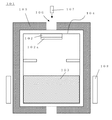
図1は、本発明の炭化珪素単結晶の製造方法を実施することができるSiC成長装置の一例を示す概略断面図である。 FIG. 1 is a schematic cross-sectional view showing an example of a SiC growth apparatus capable of carrying out the method for producing a silicon carbide single crystal of the present invention.
図1に示すように、本発明のSiC成長装置1は、種結晶基板2及び炭化珪素原材料(SiC原料ともいう)3を収容する成長容器4と、該成長容器4を囲う断熱材5と、該断熱材5に貫通して設けた温度測定用の穴(以下、単に穴ともいう)6を通して、成長容器4内の温度を測定する温度測定器7と、SiC原料を加熱するヒーター8とを備えている。
As shown in FIG. 1, the SiC growth apparatus 1 of the present invention includes a growth container 4 that houses a
成長容器4は、種結晶基板2を配置する成長室9と、SiC原料3を配置する昇華室10とからなり、例えば耐熱性のあるグラファイトで形成される。また、結晶成長の際には、不図示の石英管又はチャンバー内に成長容器4をセットして、真空排気しながらAr等の不活性ガスを供給することにより、不活性ガス雰囲気の減圧下で結晶成長(炭化珪素単結晶2aの成長)を行う。この際にn型であれば窒素を添加しても良い。
The growth vessel 4 includes a growth chamber 9 in which the
ヒーター8は、RH(抵抗加熱)又はRF(高周波)加熱を行うものを用いることができる。また、温度測定器7としては、パイロメーターを用いることで、成長容器4の外部から、断熱材5の温度測定用の穴6を通して、非接触で温度測定を精度良く行うことができる。
As the heater 8, a heater that performs RH (resistive heating) or RF (radio frequency) heating can be used. Further, by using a pyrometer as the
ここで、本発明における、SiC成長装置における種結晶基板、断熱材の温度測定用の穴の位置について詳述する。
本発明では、種結晶基板は成長容器内に配置されており、より詳しくは、図1に示すように成長容器内の上部の中心に配置されている。
また、温度測定用の穴は断熱材の上部に設けられている。より詳しくは、図1に示すように穴の中心の位置C2と、成長容器内の成長容器内の上記種結晶基板の中心の位置C1(成長容器上部の中心位置とも言い換えられる)がずれるように、種結晶基板の中心C1に対して外周側の位置にずらして穴が設けられている。
なお、断熱材上部に設けられた断熱材の外側と内側を結ぶ貫通孔である、この温度測定用の穴の中心の位置C2は、ここでは、断熱材の内側(種結晶基板側)の断面における中心位置を指す。
Here, the positions of the holes for measuring the temperature of the seed crystal substrate and the heat insulating material in the SiC growth apparatus in the present invention will be described in detail.
In the present invention, the seed crystal substrate is arranged in the growth vessel, and more specifically, it is arranged in the center of the upper part in the growth vessel as shown in FIG.
Further, a hole for measuring the temperature is provided in the upper part of the heat insulating material. More specifically, as shown in FIG. 1, the center position C2 of the hole and the center position C1 of the seed crystal substrate in the growth container in the growth container (also referred to as the center position of the upper part of the growth container) are deviated from each other. , The hole is provided at a position on the outer peripheral side with respect to the center C1 of the seed crystal substrate.
The position C2 at the center of the hole for temperature measurement, which is a through hole connecting the outside and the inside of the heat insulating material provided on the upper part of the heat insulating material, is a cross section of the inside of the heat insulating material (seed crystal substrate side). Refers to the central position in.
この断熱材の温度測定用の穴の中心位置C2が種結晶基板の中心位置C1ではなく、中心位置C1から、種結晶基板の半径の1/3の位置よりも外周側に位置するように穴が設けることが好ましい。 The hole so that the center position C2 of the hole for measuring the temperature of the heat insulating material is not the center position C1 of the seed crystal substrate but is located on the outer peripheral side from the center position C1 to the position of 1/3 of the radius of the seed crystal substrate. Is preferably provided.
このように温度測定用の穴の中心位置C2を中心位置C1から外側に配置することで、図2に示すように穴の位置に対応する種結晶基板の箇所が最も低温となり、この最も低温となる位置を種結晶基板の半径の1/3から外側にすることができる。また、この位置が炭化珪素単結晶の成長の起点となる。 By arranging the center position C2 of the hole for temperature measurement outside from the center position C1 in this way, the location of the seed crystal substrate corresponding to the position of the hole becomes the lowest temperature as shown in FIG. The position can be set to the outside from 1/3 of the radius of the seed crystal substrate. In addition, this position serves as the starting point for the growth of the silicon carbide single crystal.
以下、昇華法による本発明の炭化珪素単結晶の製造方法について図3の工程図を参照して説明する。
まず、図1のような、温度測定用の穴6の位置がずれているSiC成長装置1を用意する(工程1)。すなわち、温度測定用の穴6の中心位置C2と、後に配置する種結晶基板2の中心の位置C1(成長容器上部の中心位置)がずれるように、穴6を、種結晶基板2の中心位置C1に対して外周側の位置にずらして設けた装置を用意する。
Hereinafter, the method for producing a silicon carbide single crystal of the present invention by the sublimation method will be described with reference to the process diagram of FIG.
First, as shown in FIG. 1, a SiC growth device 1 in which the positions of the
次に、成長容器4内の昇華室10にSiC原料3を収容し(工程2)、種結晶基板2を用意して成長室9の上部の中心位置に配置する(工程3)。ここで、種結晶基板2としては、基底面である{0001}面からオフ角だけ傾斜した主面を有する炭化珪素単結晶基板を用意する。また、このオフ角の大きさは特に限定されないが、例えば0.5〜10度とすることができる。このような種結晶基板2を用いることでステップフロー成長させることができ、さらには種結晶基板2や温度測定用の穴6の配置位置、後に詳述する種結晶基板2の配置向きの関係によって、成長する炭化珪素単結晶2aにおいて、歪みや貫通欠陥を低減化することが可能である。また、上記のような値のオフ角に設定することで、より効率良くステップフロー成長させることができる。
Next, the SiC raw material 3 is housed in the
また、このときの種結晶基板2の配置の仕方(配置の向き)について、図4を参照して説明する。図4は、種結晶基板2の配置の向きを説明する図であり、ここでは簡単に、温度測定用の穴6と成長容器4の上部中心に配置した種結晶基板2のみ記載している。なお、図4は種結晶基板の中心C1と温度測定用の穴の中心C2を含む断面図である。また、種結晶基板2として基底面である{0001}面から<11−20>方向に0.5〜10度傾斜した結晶成長面を有する単結晶基板を例に挙げている。
Further, a method of arranging the seed crystal substrate 2 (direction of arrangement) at this time will be described with reference to FIG. FIG. 4 is a diagram for explaining the orientation of the arrangement of the
前述したように、種結晶基板自体は基底面からオフ角傾斜した主面を有するものである。したがって、該基底面の法線ベクトルNは種結晶基板2の主面と垂直な方向に対して傾いており、主面と垂直な方向の成分Nvと主面と平行な方向の成分Npとに分けられる。この例では主面と平行な方向の成分Npは左向きである。
ところで、温度測定用の穴の中心の位置C2について考えると、前述したように種結晶基板の中心の位置C1からずれており、このずれの方向をここでは偏芯方向Dと定義する。この例では、偏芯方向Dは左向きである。
本発明においては、図4に示すように、上記のNp(ここでは左向き)とD(ここでは左向き)とが同方向になるように、種結晶基板の向きを調整して配設する。
As described above, the seed crystal substrate itself has a main surface inclined off-angle from the basal plane. Therefore, the normal vector N of the basal plane is inclined with respect to the direction perpendicular to the main surface of the
However, considering the position C2 of the center of the hole for temperature measurement, offset from the position C1 of the center of the seed crystal base plate as described above, to define the direction of the deviation and the direction of eccentricity D here. In this example, the eccentric direction D is to the left.
In the present invention, as shown in FIG. 4, the orientation of the seed crystal substrate is adjusted and arranged so that the above Np (here, leftward) and D (here, leftward) are in the same direction.
そして、例えば、アルゴンガスと窒素ガスを流して、1〜20torr(1.3hPa〜2.7×10hPa)の圧力とし、ヒーターで加熱して2000〜2300℃の温度で、種結晶基板2上にSiC単結晶2aを成長させる(工程4)。
このとき、図4に冷却点と記載しているように、種結晶基板2において、温度測定用の穴6の位置に対応する箇所が最も低温となり、該最も低温となる位置が炭化珪素単結晶の成長の起点となる。図4の場合、冷却点よりも右側の範囲の方が、冷却点よりも左側の範囲よりも広くなっており、この広い範囲では、主面に平行な方向において、ステップフロー方向に結晶が成長していくことになる。
そして、このような本発明の製造方法によって、ウェーハ中央部において貫通欠陥が低減化され結晶性の劣化が低減化された良好な炭化珪素単結晶を製造することができる。また、従来法では製造した炭化珪素単結晶の面内で生じていた歪みを抑制することができる。
Then, for example, argon gas and nitrogen gas are flowed to bring the pressure to 1 to 20 torr (1.3 hPa to 2.7 × 10 hPa), and the
At this time, as described as a cooling point in FIG. 4, the portion of the
Then, by such a manufacturing method of the present invention, it is possible to manufacture a good silicon carbide single crystal in which penetration defects are reduced and deterioration of crystallinity is reduced in the central portion of the wafer. In addition, the strain generated in the plane of the produced silicon carbide single crystal in the conventional method can be suppressed.
なお、図1、図4においては、温度測定用の穴の中心位置C2が、種結晶基板の中心位置C1から、種結晶基板2の半径の1/2の位置付近になるように穴6を設けている例を示した。しかしながら、穴は外周側の位置にずれていれば良く、ずれの度合いは特に限定されない。ただし、前述したように穴の中心位置C2が、種結晶基板の中心位置C1から、種結晶基板の半径の1/3の位置よりも外周側に位置するものが好ましく、種結晶基板の半径の1/2の位置よりも外周側に位置するものがより好ましい。このようにすれば、実際に炭化珪素単結晶2aを種結晶基板2上に成長させるときに、より確実に、種結晶基板面内の広い範囲でステップフロー方向に炭化珪素単結晶を成長させることができる。そして、歪みや貫通欠陥がより少ない炭化珪素単結晶をより確実に得ることができる。
In addition, in FIGS. 1 and 4, the
以下、実施例及び比較例を示して本発明をより具体的に説明するが、本発明はこれらに限定されるものではない。
(実施例)
Hereinafter, the present invention will be described in more detail with reference to Examples and Comparative Examples, but the present invention is not limited thereto.
(Example)
本発明の炭化珪素単結晶の製造方法により、図1に示すSiC成長装置を用いて、以下の成長条件で直径4インチ(100mm)のSiC単結晶を成長させた。
<条件>
種結晶基板…主面が{0001}面から<11−20>方向に4°傾いた直径4インチ(100mm)のSiC単結晶基板
成長温度…2200℃
圧力…10Torr(1.3×10hPa)
雰囲気…アルゴンガス、窒素ガス
By the method for producing a silicon carbide single crystal of the present invention, a SiC single crystal having a diameter of 4 inches (100 mm) was grown under the following growth conditions using the SiC growth apparatus shown in FIG.
<Conditions>
Seed crystal substrate: SiC single crystal substrate with a diameter of 4 inches (100 mm) whose main surface is tilted 4 ° in the <11-20> direction from the {0001} plane Growth temperature: 2200 ° C.
Pressure ... 10 Torr (1.3 x 10 hPa)
Atmosphere ... Argon gas, nitrogen gas
なお、図1に示すように、温度測定用の穴が、種結晶基板の中心から、種結晶基板の半径の1/2の位置に対応する箇所に開けられ、図4に示すように、種結晶基板の基底面の結晶成長方向の法線ベクトルの種結晶基板の主面と平行な成分の方向と穴の偏芯方向が同方向となるように種結晶基板を配置して、結晶成長を行った。 As shown in FIG. 1, a hole for temperature measurement is formed from the center of the seed crystal substrate at a position corresponding to a position of 1/2 of the radius of the seed crystal substrate, and as shown in FIG. 4, the seed is formed. The seed crystal substrate is arranged so that the direction of the components parallel to the main surface of the seed crystal substrate and the eccentric direction of the holes are the same in the normal direction of the crystal growth direction of the basal plane of the crystal substrate, and the crystal growth is performed. went.
SiC単結晶成長後、マルチワイヤーソーにてウェーハを切り出し、研削、鏡面研磨およびCMP研磨後、光弾性評価により面内歪み分布を調査した結果を図5に示す。 FIG. 5 shows the results of investigating the in-plane strain distribution by photoelastic evaluation after cutting out a wafer with a multi-wire saw after growing a SiC single crystal, grinding, mirror polishing, and CMP polishing.
更に、ウェーハ中央部の結晶性を調査した結果を表1に示す。
(比較例)
Further, Table 1 shows the results of investigating the crystallinity of the central portion of the wafer.
(Comparison example)
図7のようなSiC成長装置を用意し、従来の炭化珪素単結晶の製造方法で炭化珪素単結晶を製造した。図7に示すように、温度測定用の穴の中心位置が種結晶基板の中心に一致するように、穴が開けられている装置を用い、主面が{0001}面のSiC単結晶基板を種結晶基板として用いたことを除き、実施例と同じ条件で直径4インチ(100mm)のSiC単結晶を成長させた。 A SiC growth apparatus as shown in FIG. 7 was prepared, and a silicon carbide single crystal was produced by a conventional method for producing a silicon carbide single crystal. As shown in FIG. 7, a SiC single crystal substrate having a main surface of {0001} plane is used by using a device in which holes are formed so that the center position of the hole for temperature measurement coincides with the center of the seed crystal substrate. A SiC single crystal having a diameter of 4 inches (100 mm) was grown under the same conditions as in the examples except that it was used as a seed crystal substrate.
SiC単結晶成長後、マルチワイヤーソーにてウェーハを切り出し、研削、鏡面研磨およびCMP研磨後に、光弾性評価により面内歪み分布を調査した結果を図6に示す。更に、実施例と同様にしてウェーハ中央部の結晶性を調査した結果を表1に示す。 FIG. 6 shows the results of investigating the in-plane strain distribution by photoelasticity evaluation after cutting out a wafer with a multi-wire saw after growing a SiC single crystal, grinding, mirror polishing, and CMP polishing. Further, Table 1 shows the results of investigating the crystallinity of the central portion of the wafer in the same manner as in the examples.

図5、6に示す結果から、実施例は、比較例に比べて、ウェーハの面内中央部及び外周部の歪みが弱まっていることが分かる。
また、表1から、実施例における各座標の半値幅は、比較例よりも顕著に小さい値となり、実施例のウェーハは比較例に比べて平坦な面を有し、結晶性が改善されているのが判る。
From the results shown in FIGS. 5 and 6, it can be seen that in the examples, the distortions in the in-plane central portion and the outer peripheral portion of the wafer are weaker than those in the comparative example.
Further, from Table 1, the full width at half maximum of each coordinate in the example is remarkably smaller than that of the comparative example, and the wafer of the example has a flat surface as compared with the comparative example, and the crystallinity is improved. I understand that.
なお、本発明は、上記実施形態に限定されるものではない。上記実施形態は例示であり、本発明の特許請求の範囲に記載された技術的思想と実質的に同一な構成を有し、同様な作用効果を奏するものは、いかなるものであっても本発明の技術的範囲に包含される。 The present invention is not limited to the above embodiment. The above-described embodiment is an example, and any object having substantially the same configuration as the technical idea described in the claims of the present invention and exhibiting the same effect and effect is the present invention. Is included in the technical scope of.
1、101…SiC成長装置、 2、102…種結晶基板、
2a、102a…炭化珪素単結晶、 3、103…炭化珪素原材料、
4、104…成長容器、 5、105…断熱材、 6、106…温度測定用の穴、
7、107…温度測定器、 8、108…ヒーター、 9…成長室、 10…昇華室、
C1…種結晶基板の中心の位置、 C2…温度測定用の穴の中心の位置、
N…種結晶基板の基底面の法線ベクトル、
Nv…法線ベクトルの主面と垂直な方向の成分、
Np…法線ベクトルの主面と平行な方向の成分、
D…温度測定用の穴の偏芯方向。
1, 101 ... SiC growth device, 2, 102 ... seed crystal substrate,
2a, 102a ... Silicon carbide single crystal, 3,103 ... Silicon carbide raw material,
4, 104 ... Growth container, 5, 105 ... Insulation material, 6, 106 ... Hole for temperature measurement,
7,107 ... Temperature measuring instrument, 8,108 ... Heater, 9 ... Growth chamber, 10 ... Sublimation chamber,
C1 ... The position of the center of the seed crystal substrate, C2 ... The position of the center of the hole for temperature measurement,
N ... Normal vector of the basal plane of the seed crystal substrate,
Nv: A component in the direction perpendicular to the main plane of the normal vector,
Np: A component in the direction parallel to the main surface of the normal vector,
D ... Eccentric direction of the hole for temperature measurement.
Claims (3)
前記断熱材の温度測定用の穴の中心の位置と前記成長容器内に配置する前記種結晶基板の中心の位置がずれるように、前記温度測定用の穴を、前記成長容器内に配置する前記種結晶基板の中心に対して外周側の位置にずらして設け、
前記種結晶基板として、基底面である{0001}面からオフ角だけ傾斜した主面を有する炭化珪素単結晶基板を用い、
前記成長容器内の前記種結晶基板の中心と前記断熱材の前記温度測定用の穴の中心を含む断面視において、前記種結晶基板の基底面の法線ベクトルの前記種結晶基板の主面と平行な成分の方向と、前記温度測定用の穴の中心の前記種結晶基板の中心に対する偏芯方向とが、同方向になるように前記種結晶基板を前記成長容器内に配置して、前記炭化珪素単結晶を成長させることを特徴とする炭化珪素単結晶の製造方法。 The growth container is surrounded by a heat insulating material provided with a hole for temperature measurement at the upper part, the seed crystal substrate is arranged at the center of the upper part in the growth container, the silicon carbide raw material is arranged at the lower part of the growth container, and the silicon carbide is arranged. A method for producing a silicon carbide single crystal in which a raw material is sublimated to grow a silicon carbide single crystal on the seed crystal substrate.
The hole for temperature measurement is arranged in the growth container so that the position of the center of the hole for temperature measurement of the heat insulating material and the position of the center of the seed crystal substrate arranged in the growth container deviate from each other. The seed crystal substrate is provided so as to be offset from the center of the seed crystal substrate to the outer peripheral side.
As the seed crystal substrate, a silicon carbide single crystal substrate having a main surface inclined by an off angle from the {0001} plane which is the basal plane is used.
In a cross-sectional view including the center of the seed crystal substrate in the growth vessel and the center of the hole for temperature measurement of the heat insulating material, the main surface of the seed crystal substrate having the normal vector of the basal plane of the seed crystal substrate. The seed crystal substrate is arranged in the growth vessel so that the directions of the parallel components and the eccentric direction of the center of the hole for temperature measurement with respect to the center of the seed crystal substrate are in the same direction. A method for producing a silicon carbide single crystal, which comprises growing a silicon carbide single crystal.
Priority Applications (7)
| Application Number | Priority Date | Filing Date | Title |
|---|---|---|---|
| JP2018045227A JP6879236B2 (en) | 2018-03-13 | 2018-03-13 | Method for manufacturing silicon carbide single crystal |
| EP19768426.9A EP3767016A4 (en) | 2018-03-13 | 2019-02-15 | Method for producing silicon carbide single crystal |
| US16/980,144 US11225729B2 (en) | 2018-03-13 | 2019-02-15 | Method for manufacturing a silicon carbide single crystal by adjusting the position of a hole in a top of the growth container relative to the off angle of the silicon carbide substrate |
| KR1020207026353A KR102631661B1 (en) | 2018-03-13 | 2019-02-15 | Manufacturing method of silicon carbide single crystal |
| CN201980018916.0A CN111868310B (en) | 2018-03-13 | 2019-02-15 | Method for producing silicon carbide single crystal |
| PCT/JP2019/005690 WO2019176444A1 (en) | 2018-03-13 | 2019-02-15 | Method for producing silicon carbide single crystal |
| TW108105919A TWI815863B (en) | 2018-03-13 | 2019-02-22 | Manufacturing method of silicon carbide single crystal |
Applications Claiming Priority (1)
| Application Number | Priority Date | Filing Date | Title |
|---|---|---|---|
| JP2018045227A JP6879236B2 (en) | 2018-03-13 | 2018-03-13 | Method for manufacturing silicon carbide single crystal |
Publications (2)
| Publication Number | Publication Date |
|---|---|
| JP2019156679A JP2019156679A (en) | 2019-09-19 |
| JP6879236B2 true JP6879236B2 (en) | 2021-06-02 |
Family
ID=67907649
Family Applications (1)
| Application Number | Title | Priority Date | Filing Date |
|---|---|---|---|
| JP2018045227A Active JP6879236B2 (en) | 2018-03-13 | 2018-03-13 | Method for manufacturing silicon carbide single crystal |
Country Status (7)
| Country | Link |
|---|---|
| US (1) | US11225729B2 (en) |
| EP (1) | EP3767016A4 (en) |
| JP (1) | JP6879236B2 (en) |
| KR (1) | KR102631661B1 (en) |
| CN (1) | CN111868310B (en) |
| TW (1) | TWI815863B (en) |
| WO (1) | WO2019176444A1 (en) |
Families Citing this family (2)
| Publication number | Priority date | Publication date | Assignee | Title |
|---|---|---|---|---|
| KR102284879B1 (en) * | 2019-10-29 | 2021-07-30 | 에스케이씨 주식회사 | SiC WAFER, PREPARATION METHOD OF SiC WAFER |
| CN111958070B (en) * | 2020-10-22 | 2021-02-02 | 中电化合物半导体有限公司 | Preparation method of low-defect-density silicon carbide single crystal substrate |
Family Cites Families (15)
| Publication number | Priority date | Publication date | Assignee | Title |
|---|---|---|---|---|
| JP4230035B2 (en) | 1998-12-25 | 2009-02-25 | 昭和電工株式会社 | Silicon carbide single crystal and method for producing the same |
| US7601441B2 (en) * | 2002-06-24 | 2009-10-13 | Cree, Inc. | One hundred millimeter high purity semi-insulating single crystal silicon carbide wafer |
| JP2005239465A (en) | 2004-02-25 | 2005-09-08 | Matsushita Electric Ind Co Ltd | Silicon carbide single crystal production device |
| US7192482B2 (en) | 2004-08-10 | 2007-03-20 | Cree, Inc. | Seed and seedholder combinations for high quality growth of large silicon carbide single crystals |
| JP4926556B2 (en) * | 2006-06-20 | 2012-05-09 | 新日本製鐵株式会社 | Method for manufacturing silicon carbide single crystal ingot and silicon carbide single crystal substrate |
| JP5482643B2 (en) * | 2010-12-24 | 2014-05-07 | 新日鐵住金株式会社 | Silicon carbide single crystal ingot manufacturing equipment |
| CN104246023B (en) | 2012-04-20 | 2019-02-01 | 贰陆股份公司 | The SiC single crystal of major diameter high-quality, method and apparatus |
| JP6183010B2 (en) | 2013-07-03 | 2017-08-23 | 住友電気工業株式会社 | Silicon carbide single crystal substrate and method for manufacturing the same |
| WO2015182246A1 (en) | 2014-05-29 | 2015-12-03 | 住友電気工業株式会社 | Silicon-carbide-ingot manufacturing method, silicon-carbide seed substrate, and silicon-carbide substrate |
| US9279192B2 (en) * | 2014-07-29 | 2016-03-08 | Dow Corning Corporation | Method for manufacturing SiC wafer fit for integration with power device manufacturing technology |
| JP6259740B2 (en) | 2014-09-11 | 2018-01-10 | 国立大学法人名古屋大学 | Silicon carbide crystal manufacturing method and crystal manufacturing apparatus |
| US20160138185A1 (en) * | 2014-11-18 | 2016-05-19 | Sumitomo Electric Industries, Ltd. | Method of manufacturing silicon carbide single crystal |
| WO2016088883A1 (en) * | 2014-12-05 | 2016-06-09 | 新日鐵住金株式会社 | Method for producing silicon carbide single crystal, and silicon carbide single crystal substrate |
| JP6584007B2 (en) * | 2015-12-10 | 2019-10-02 | 昭和電工株式会社 | Single crystal manufacturing method and single crystal manufacturing apparatus |
| JP6915526B2 (en) * | 2017-12-27 | 2021-08-04 | 信越半導体株式会社 | Method for manufacturing silicon carbide single crystal |
-
2018
- 2018-03-13 JP JP2018045227A patent/JP6879236B2/en active Active
-
2019
- 2019-02-15 US US16/980,144 patent/US11225729B2/en active Active
- 2019-02-15 CN CN201980018916.0A patent/CN111868310B/en active Active
- 2019-02-15 WO PCT/JP2019/005690 patent/WO2019176444A1/en unknown
- 2019-02-15 KR KR1020207026353A patent/KR102631661B1/en active IP Right Grant
- 2019-02-15 EP EP19768426.9A patent/EP3767016A4/en active Pending
- 2019-02-22 TW TW108105919A patent/TWI815863B/en active
Also Published As
| Publication number | Publication date |
|---|---|
| CN111868310A (en) | 2020-10-30 |
| EP3767016A1 (en) | 2021-01-20 |
| US11225729B2 (en) | 2022-01-18 |
| TW201938853A (en) | 2019-10-01 |
| JP2019156679A (en) | 2019-09-19 |
| KR102631661B1 (en) | 2024-02-01 |
| EP3767016A4 (en) | 2021-11-24 |
| KR20200128680A (en) | 2020-11-16 |
| CN111868310B (en) | 2021-12-24 |
| WO2019176444A1 (en) | 2019-09-19 |
| US20210010157A1 (en) | 2021-01-14 |
| TWI815863B (en) | 2023-09-21 |
Similar Documents
| Publication | Publication Date | Title |
|---|---|---|
| KR102284879B1 (en) | SiC WAFER, PREPARATION METHOD OF SiC WAFER | |
| US11131038B2 (en) | Furnace for seeded sublimation of wide band gap crystals | |
| JP6183010B2 (en) | Silicon carbide single crystal substrate and method for manufacturing the same | |
| US10837123B2 (en) | Method of manufacturing SiC ingot | |
| JP6879236B2 (en) | Method for manufacturing silicon carbide single crystal | |
| JP6915526B2 (en) | Method for manufacturing silicon carbide single crystal | |
| JP6748613B2 (en) | Silicon carbide single crystal substrate | |
| KR100775983B1 (en) | GROWING METHOD OF SEMI-INSULATING SiC SINGLE CRYSTAL | |
| JP4552516B2 (en) | Method for producing AlN single crystal | |
| US20210010161A1 (en) | Method for manufacturing silicon carbide single crystal | |
| CN116411339A (en) | High-quality silicon carbide single crystal growth method | |
| JP2018118873A (en) | Method for manufacturing nitride semiconductor substrate |
Legal Events
| Date | Code | Title | Description |
|---|---|---|---|
| A521 | Written amendment |
Free format text: JAPANESE INTERMEDIATE CODE: A523 Effective date: 20190215 |
|
| A621 | Written request for application examination |
Free format text: JAPANESE INTERMEDIATE CODE: A621 Effective date: 20200220 |
|
| TRDD | Decision of grant or rejection written | ||
| A01 | Written decision to grant a patent or to grant a registration (utility model) |
Free format text: JAPANESE INTERMEDIATE CODE: A01 Effective date: 20210330 |
|
| A61 | First payment of annual fees (during grant procedure) |
Free format text: JAPANESE INTERMEDIATE CODE: A61 Effective date: 20210412 |
|
| R150 | Certificate of patent or registration of utility model |
Ref document number: 6879236 Country of ref document: JP Free format text: JAPANESE INTERMEDIATE CODE: R150 |