JP6878300B2 - Improved virtual GPIO with multi-mode modulation - Google Patents
Improved virtual GPIO with multi-mode modulation Download PDFInfo
- Publication number
- JP6878300B2 JP6878300B2 JP2017553087A JP2017553087A JP6878300B2 JP 6878300 B2 JP6878300 B2 JP 6878300B2 JP 2017553087 A JP2017553087 A JP 2017553087A JP 2017553087 A JP2017553087 A JP 2017553087A JP 6878300 B2 JP6878300 B2 JP 6878300B2
- Authority
- JP
- Japan
- Prior art keywords
- gpio
- messaging
- bit
- signal
- pulse width
- Prior art date
- Legal status (The legal status is an assumption and is not a legal conclusion. Google has not performed a legal analysis and makes no representation as to the accuracy of the status listed.)
- Active
Links
Images


Classifications
-
- G—PHYSICS
- G06—COMPUTING; CALCULATING OR COUNTING
- G06F—ELECTRIC DIGITAL DATA PROCESSING
- G06F13/00—Interconnection of, or transfer of information or other signals between, memories, input/output devices or central processing units
- G06F13/14—Handling requests for interconnection or transfer
- G06F13/16—Handling requests for interconnection or transfer for access to memory bus
- G06F13/1668—Details of memory controller
- G06F13/1678—Details of memory controller using bus width
-
- G—PHYSICS
- G06—COMPUTING; CALCULATING OR COUNTING
- G06F—ELECTRIC DIGITAL DATA PROCESSING
- G06F13/00—Interconnection of, or transfer of information or other signals between, memories, input/output devices or central processing units
- G06F13/38—Information transfer, e.g. on bus
- G06F13/382—Information transfer, e.g. on bus using universal interface adapter
- G06F13/385—Information transfer, e.g. on bus using universal interface adapter for adaptation of a particular data processing system to different peripheral devices
-
- G—PHYSICS
- G06—COMPUTING; CALCULATING OR COUNTING
- G06F—ELECTRIC DIGITAL DATA PROCESSING
- G06F13/00—Interconnection of, or transfer of information or other signals between, memories, input/output devices or central processing units
- G06F13/38—Information transfer, e.g. on bus
- G06F13/42—Bus transfer protocol, e.g. handshake; Synchronisation
- G06F13/4282—Bus transfer protocol, e.g. handshake; Synchronisation on a serial bus, e.g. I2C bus, SPI bus
-
- H—ELECTRICITY
- H03—ELECTRONIC CIRCUITRY
- H03M—CODING; DECODING; CODE CONVERSION IN GENERAL
- H03M13/00—Coding, decoding or code conversion, for error detection or error correction; Coding theory basic assumptions; Coding bounds; Error probability evaluation methods; Channel models; Simulation or testing of codes
- H03M13/03—Error detection or forward error correction by redundancy in data representation, i.e. code words containing more digits than the source words
- H03M13/05—Error detection or forward error correction by redundancy in data representation, i.e. code words containing more digits than the source words using block codes, i.e. a predetermined number of check bits joined to a predetermined number of information bits
- H03M13/13—Linear codes
- H03M13/19—Single error correction without using particular properties of the cyclic codes, e.g. Hamming codes, extended or generalised Hamming codes
-
- Y—GENERAL TAGGING OF NEW TECHNOLOGICAL DEVELOPMENTS; GENERAL TAGGING OF CROSS-SECTIONAL TECHNOLOGIES SPANNING OVER SEVERAL SECTIONS OF THE IPC; TECHNICAL SUBJECTS COVERED BY FORMER USPC CROSS-REFERENCE ART COLLECTIONS [XRACs] AND DIGESTS
- Y02—TECHNOLOGIES OR APPLICATIONS FOR MITIGATION OR ADAPTATION AGAINST CLIMATE CHANGE
- Y02D—CLIMATE CHANGE MITIGATION TECHNOLOGIES IN INFORMATION AND COMMUNICATION TECHNOLOGIES [ICT], I.E. INFORMATION AND COMMUNICATION TECHNOLOGIES AIMING AT THE REDUCTION OF THEIR OWN ENERGY USE
- Y02D10/00—Energy efficient computing, e.g. low power processors, power management or thermal management
Description
関連出願の相互参照
本出願は、2015年4月14日に出願された仮出願第62/147,238号の利益を主張し、2015年9月25日に出願された米国仮出願第62/233,278号の利益をさらに主張する、2016年4月12日に出願された米国出願第15/097,237号の利益を主張する。
Cross-reference to related applications This application claims the interests of Provisional Application No. 62 / 147,238 filed on April 14, 2015, and US Provisional Application No. 62 / 233,278 filed on September 25, 2015. Claim the interests of US Application No. 15 / 097,237 filed on April 12, 2016.
本出願は、シグナリングに関し、より詳細には、パルス幅変調と位相変調を組み合わせるマルチ変調デジタルシグナリング方式に関する。 The present application relates to signaling, and more particularly to a multimodulation digital signaling scheme that combines pulse width modulation and phase modulation.
汎用入力/出力(GPIO)により、集積回路設計者が特定のアプリケーション向けにカスタマイズされ得る汎用ピンを実現することが可能になる。たとえば、GPIOピンは、ユーザのニーズに応じて出力ピンまたは入力ピンのいずれかであるようにプログラム可能である。GPIOのホストまたは周辺装置は、一般に、インターフェース要件に基づいて変化することができるピンのグループを制御する。GPIOピンはプログラム可能であるので、マイクロプロセッサおよびマイクロコントローラのアプリケーションに含まれることが多い。たとえば、モバイルデバイス内のアプリケーションプロセッサは、モデムプロセッサとのプロセッサ間通信(IPC)などのハンドシェイクシグナリングを行うために、いくつかのGPIOピンを使用してもよい。 General-purpose input / output (GPIO) enables integrated circuit designers to implement general-purpose pins that can be customized for specific applications. For example, GPIO pins can be programmed to be either output pins or input pins depending on the needs of the user. GPIO hosts or peripherals generally control a group of pins that can vary based on interface requirements. GPIO pins are programmable and are often included in microprocessor and microcontroller applications. For example, an application processor in a mobile device may use several GPIO pins to perform handshake signaling such as interprocessor communication (IPC) with a modem processor.
そのようなハンドシェイクシグナリングに関して、側波帯信号は、プロセッサによって送信と受信の両方が行われなければならない場合、「対称」と見なされる。交換される必要があるn個の対称側波帯信号が存在する場合、各プロセッサは、n*2個のGPIO(所与の信号を送信する1つのGPIOおよびその信号を受信する1つのGPIO)を必要とする。たとえば、モデムプロセッサとアプリケーションプロセッサとの間の対称IPCインターフェースは、5つの信号を備える場合があり、このことは、結果として生じるIPCシグナリングに10個のGPIOピンが必要であることになる。IPC通信にはそれほど多くのGPIOピンが必要なので、製造コストが増大する。さらに、IPCに充てるGPIOが多すぎると、他のシステムレベルの周辺インターフェースに対するGPIOの利用可能性が制限される。この問題は、特定のコーナー条件が侵害されることになるという点で、プロセッサ間のメインデータバスにIPC通信を移動させることによって解決することができない。 For such handshake signaling, sideband signals are considered "symmetrical" if both transmission and reception must be done by the processor. If there are n symmetric sideband signals that need to be exchanged, each processor will have n * 2 GPIOs (one GPIO sending a given signal and one GPIO receiving that signal). Needs. For example, a symmetric IPC interface between a modem processor and an application processor may have 5 signals, which would require 10 GPIO pins for the resulting IPC signaling. IPC communication requires so many GPIO pins, which increases manufacturing costs. In addition, too much GPIO for IPC limits the availability of GPIO to other system-level peripheral interfaces. This problem cannot be solved by moving IPC communication to the main data bus between processors in that certain corner conditions will be violated.
加えて、モバイルデバイスなどのシステム内の集積回路間の通信をサポートするために、いくつかのデジタルシグナリングプロトコルが開発されてきた。これらのシグナリングプロトコルは、本明細書では、送信回路がその送信ピンを電源電圧レベルまで高くするか、またはビットを送信するためにピンを接地するかのいずれかであるという点で、「デジタル」と見なされる。そのようなデジタルシグナリングプロトコルの例としては、汎用I/O(GPIO)およびユニバーサル非同期受信機送信機(UART:universal asynchronous receiver transmitter)がある。たとえば、UART送信機は、UART受信機における受信ピン上で受信されるデジタル信号を送信ピンを介して駆動する。UART受信機は、受信された信号がバイナリ高であったか、またはバイナリ低であったかを判定するために、受信された信号をオーバーサンプリングクロックを使用してサンプリングする。 In addition, several digital signaling protocols have been developed to support communication between integrated circuits in systems such as mobile devices. These signaling protocols are "digital" herein in that the transmit circuit either raises its transmit pins to power supply voltage levels or grounds the pins to transmit bits. Is considered. Examples of such digital signaling protocols are general purpose input / O (GPIO) and universal asynchronous receiver transmitter (UART). For example, a UART transmitter drives a digital signal received on a receive pin in a UART receiver via a transmit pin. The UART receiver uses an oversampling clock to sample the received signal to determine if the received signal was binary high or binary low.
これらのデジタルシグナリングプロトコルにおける電力消費を低減するために、ランレングス符号化(RLE:run length encoding)などの様々な可逆データ圧縮技法が利用されてきた。しかし、圧縮の程度はデータのランダム性に依存するので、ランレングス符号化は固定された予測可能なスループット向上を保証しない。データ送信が完全にランダムである場合、ランレングス符号化は、いかなる利益も提供しない。他のより複雑な方式は、改善されたスループットを提供するが、デジタルシグナリングに適合しない。たとえば、直交位相シフトキー(QPSK)方式の使用は、従来のデジタルシグナリングの2倍のスループットを有するが、2つの独立した正弦波サブキャリアの使用を必要とする。対照的に、送信機は、シンボル送信の間、その送信ピンを電源電圧におよび/または接地に駆動する必要があるにすぎないので、デジタル信号プロトコルは、はるかに単純である。同様に、デジタルシグナリング受信機は、オーバーサンプリングクロックの各サンプリングにおいて電圧高信号が受信されているか、または電圧低信号が受信されているかを判定する必要があるにすぎない。 Various lossless data compression techniques such as run length encoding (RLE) have been used to reduce power consumption in these digital signaling protocols. However, run-length coding does not guarantee a fixed and predictable throughput increase, as the degree of compression depends on the randomness of the data. Run-length coding does not provide any benefit if the data transmission is completely random. Other more complex schemes provide improved throughput, but are not compatible with digital signaling. For example, the use of the Quadrature Phase Shift Keying (QPSK) scheme has twice the throughput of traditional digital signaling, but requires the use of two independent sinusoidal subcarriers. In contrast, the digital signal protocol is much simpler because the transmitter only needs to drive its transmit pins to supply voltage and / or ground during symbol transmission. Similarly, the digital signaling receiver only needs to determine if a high voltage signal is being received or a low voltage signal is being received at each sampling of the oversampling clock.
したがって、当技術分野では、過度の数のピンを必要とすることなしに多数の入力/出力信号を適応させることができ、スループットが向上し電力消費が低減された改善されたデジタルシグナリングプロトコルを使用する、GPIOアーキテクチャが必要とされている。 Therefore, the art uses improved digital signaling protocols that allow a large number of input / output signals to be adapted without the need for an excessive number of pins, resulting in higher throughput and reduced power consumption. The GPIO architecture is required.
ハイブリッド仮想GPIOアーキテクチャは、各々がプロセッサを有する2つの集積回路の間の通信のために提供される。このアーキテクチャは、GPIO信号とメッセージング信号の両方を適応させるという点で「ハイブリッド」と見なされる。前に説明したように、従来のGPIOシステムにおけるGPIO信号は、特定のピン専用である。対応するGPIOピン上でのGPIO信号の受信は、受信プロセッサへの信号を識別する。しかし、本明細書で定義するメッセージング信号は、シリアル周辺インターフェース(SPI)またはプロセス間通信(IPC)インターフェースなどにおける専用受信ピン上で受信される信号である。したがって、様々なメッセージング信号は、同じ専用受信ピン上で受信され得る。メッセージング信号を区別するために、メッセージング信号がアドレスを含んでいるアドレスヘッダを含むことが一般的である。受信集積回路は、アドレスに基づいて、受信されたメッセージング信号を適切なレジスタにルーティングする。たとえば、1つのタイプのメッセージング信号は、ワイヤレスカードまたはGPSカードなどのインストールされたカードの識別情報に関係してもよい。次いで、そのようなメッセージング信号は、適切なレジスタにマッピングするアドレスを有することになり、その結果、対応するメッセージコンテンツは、それに応じて登録され得る。次いで、レジスタの結果として生じるコンテンツを解釈することによって、受信プロセッサは、インストールされたカードの識別情報を解釈することができる。他のタイプのメッセージング信号は、類似する方法で受信集積回路内の適切なレジスタにルーティングされることになる。 The hybrid virtual GPIO architecture is provided for communication between two integrated circuits, each with a processor. This architecture is considered "hybrid" in that it adapts both GPIO and messaging signals. As explained earlier, GPIO signals in traditional GPIO systems are dedicated to a particular pin. Receiving a GPIO signal on the corresponding GPIO pin identifies the signal to the receiving processor. However, the messaging signal as defined herein is a signal received on a dedicated receive pin, such as in a serial peripheral interface (SPI) or interprocess communication (IPC) interface. Therefore, various messaging signals can be received on the same dedicated receive pin. In order to distinguish the messaging signal, it is common for the messaging signal to include an address header containing the address. The receive integrated circuit routes the received messaging signal to the appropriate register based on the address. For example, one type of messaging signal may relate to the identity of an installed card, such as a wireless card or GPS card. Such messaging signals will then have an address that maps to the appropriate register, so that the corresponding message content can be registered accordingly. By interpreting the content that results from the register, the receiving processor can then interpret the identification information of the installed card. Other types of messaging signals will be routed to the appropriate registers in the receiving integrated circuit in a similar manner.
各集積回路は、GPIO信号の送信セットを使用して(1つまたは複数の)残りの集積回路と通信するための仮想GPIOインターフェースも含む。仮想GPIOインターフェースは、従来の方法でGPIOピンを介して送信セットの一部分を対向する集積回路内のリモートプロセッサに送信するように構成される。しかし、送信セットの残りの部分は、個々のGPIOピン上では送信されない。代わりに、GPIO信号の送信セットの残りの部分は、ハイブリッド仮想GPIO有限状態機械(FSM)によって少なくとも1つのフレーム中に直列化され、専用送信ピンを介して送信される。ハイブリッド仮想GPIO有限状態機械はまた、メッセージング信号を少なくとも1つのフレーム中にまたはメッセージング信号の専用フレーム中に直列化するように構成される。 Each integrated circuit also includes a virtual GPIO interface for communicating with the remaining integrated circuits (s) using the transmission set of GPIO signals. The virtual GPIO interface is configured to transmit a portion of the transmit set via GPIO pins to a remote processor in an opposing integrated circuit in a traditional manner. However, the rest of the transmit set is not transmitted on individual GPIO pins. Instead, the rest of the GPIO signal transmission set is serialized in at least one frame by a hybrid virtual GPIO finite state machine (FSM) and transmitted via a dedicated transmit pin. The hybrid virtual GPIO finite state machine is also configured to serialize the messaging signal in at least one frame or in a dedicated frame of the messaging signal.
各集積回路は、残りの集積回路内のオーバーサンプリングクロックと非同期であるオーバーサンプリングクロックも含む。集積回路のハイブリッド仮想FSMは、そのオーバーサンプリングクロックのサイクルに応答して、仮想GPIO信号のフレームおよび/またはメッセージング信号のフレームを送信および受信するように構成される。送信ハイブリッド仮想FSMは、オーバーサンプリングクロックを使用してビットをオーバーサンプリングし、結果として生じるサンプルを送信ピンを介してリモート集積回路内のハイブリッド仮想FSMの受信ピンに送信することによって、送信されるべきフレーム中で各ビットをその送信ピンを介して送信する。受信ハイブリッド仮想FSMは、そのオーバーサンプリングクロックを使用して各受信されたビットをサンプリングし、UARTの分野において知られているように、結果として生じるサンプルに基づいてビットを復号する。結果として生じるアーキテクチャは、単一の送信ピンおよび単一の受信ピンだけを使用して仮想GPIO信号およびメッセージング信号の結果として生じる送信を同期させるために外部クロックピンを必要としないので、非常に有利である。 Each integrated circuit also includes an oversampling clock that is asynchronous with the oversampling clock in the remaining integrated circuits. An integrated circuit hybrid virtual FSM is configured to send and receive frames of virtual GPIO signals and / or frames of messaging signals in response to cycles of its oversampling clock. The transmit hybrid virtual FSM should be transmitted by oversampling the bits using an oversampling clock and transmitting the resulting sample through the transmit pin to the receive pin of the hybrid virtual FSM in the remote integrated circuit. Send each bit in the frame through its transmit pin. The receive hybrid virtual FSM uses its oversampling clock to sample each received bit and decode the bit based on the resulting sample, as is known in the field of UART. The resulting architecture is very advantageous as it does not require an external clock pin to synchronize the resulting transmission of virtual GPIO and messaging signals using only a single transmit pin and a single receive pin. Is.
仮想GPIO送信を向上させるために、各ハイブリッド仮想GPIO(VGPIO)インターフェースは、位相符号化パルス幅変調シンボルを使用してフレームビットを送信および受信するようにさらに構成される。たとえば、シンボルが2つの考えられるパルス幅を有すると仮定する。従来のパルス幅変調方式では、これらの2つのパルス幅は1ビットを表すことになる。しかし、加えて、シンボルは、少なくとも2つの考えられる位相も有する。2位相実施形態では、パルスは、ビット周期の終わりに整合された、それらの立下りエッジを有するか、またはビット周期の始めに整合された、それらの立上りエッジを有するかのいずれかであるように整合される。したがって、2位相整合は、別のビットを表す。パルス幅変調と位相変調の両方のこの組合せを仮定すると、結果として生じるシンボルは、本明細書では「マルチ変調」シンボルまたは「マルチ変調」ワードとして示される。これらのワードは、増加したスループットおよび低減された電力消費により、バイナリ位相変調方式またはパルス幅変調方式と比較して非常に有利である。さらに、これらの利点は、従来のデジタルシグナリング技法から逸脱することなく得られる。したがって、QPSKなどにおけるアナログ正弦曲線に関わる複雑性が回避される。 To improve virtual GPIO transmission, each hybrid virtual GPIO (VGPIO) interface is further configured to transmit and receive frame bits using phase coded pulse width modulation symbols. For example, suppose the symbol has two possible pulse widths. In the conventional pulse width modulation method, these two pulse widths represent 1 bit. However, in addition, the symbol also has at least two possible phases. In a two-phase embodiment, the pulses are either such that they have their falling edges matched at the end of the bit period, or they have their rising edges matched at the beginning of the bit period. Is consistent with. Therefore, two-phase matching represents another bit. Assuming this combination of both pulse width modulation and phase modulation, the resulting symbols are referred to herein as "multi-modulation" symbols or "multi-modulation" words. These words have a great advantage over binary phase modulation or pulse width modulation schemes due to their increased throughput and reduced power consumption. Moreover, these advantages are obtained without departing from traditional digital signaling techniques. Therefore, the complexity associated with analog sinusoidal curves in QPSK and the like is avoided.
開示するハイブリッド仮想GPIOアーキテクチャのための2つの主要な実施形態が存在する。第1の実施形態では、専用送信ピンを介して送信される各フレームは、フレームが仮想GPIO信号の送信セットを備えるかまたはメッセージング信号の送信セットを備えるかを識別するヘッダを含む。ヘッダはまた、フレームが受信機側で設定されるべき仮想GPIOフレーム長を識別することを示してもよく、または所望の仮想GPIOフレーム長の確認を示してもよい。したがって、フレームサイズは可変であり、結果として生じるストリーム長決定フレームによって決定される。第2の実施形態では、ヘッダは、仮想GPIO信号とメッセージング信号の両方を含むフレームにわたって拡張され、その結果、拡張されたヘッダは、仮想GPIO信号およびメッセージング信号のビット位置を識別する。次いで、ハイブリッドGPIOインターフェースは、リモートプロセッサからのGPIO信号およびメッセージング信号の第2のセットを備える信号の第2のセットを受信プロセッサに供給することができる。 There are two main embodiments for the hybrid virtual GPIO architecture to be disclosed. In the first embodiment, each frame transmitted via the dedicated transmit pin includes a header that identifies whether the frame comprises a transmission set of virtual GPIO signals or a transmission set of messaging signals. The header may also indicate that the frame identifies a virtual GPIO frame length that should be set on the receiver side, or may indicate confirmation of the desired virtual GPIO frame length. Therefore, the frame size is variable and is determined by the resulting stream length determination frame. In the second embodiment, the header is extended over a frame containing both the virtual GPIO signal and the messaging signal, so that the extended header identifies the bit positions of the virtual GPIO signal and the messaging signal. The hybrid GPIO interface can then supply the receiving processor with a second set of signals, including a second set of GPIO and messaging signals from the remote processor.
ハイブリッド仮想GPIO FSMは、各々がスタートビットおよびエンドビットによって画定されたフレーム中で、仮想GPIO信号およびメッセージング信号の送信セットを送信する。したがって、受信デバイス内のハイブリッド仮想GPIO FSMは、送信されたフレームを、仮想GPIO信号およびメッセージング信号のその受信セットとして受信する。あるプロセッサ用のFSMは、そのFSMがスタートビットとエンドビットの両方を含む完全なフレームを受信したかどうかを監視することによって、リモートプロセッサが失敗したかどうかを検出することができる。 The hybrid virtual GPIO FSM transmits a transmission set of virtual GPIO and messaging signals, each in a frame defined by a start bit and an end bit. Therefore, the hybrid virtual GPIO FSM in the receiving device receives the transmitted frame as its reception set of virtual GPIO and messaging signals. An FSM for a processor can detect if a remote processor has failed by monitoring whether the FSM has received a complete frame containing both the start and end bits.
これらの利点および追加の利点は、以下の詳細な説明を通してより良く諒解され得る。 These advantages and additional advantages can be better understood through the detailed description below.
本開示の実施形態およびそれらの利点は、以下の詳細な説明を参照することによって最も良く理解される。図のうちの1つまたは複数に示す同様の要素を識別するために同様の参照番号が使用されることを諒解されたい。 The embodiments of the present disclosure and their advantages are best understood by reference to the detailed description below. Please understand that similar reference numbers are used to identify similar elements shown in one or more of the figures.
たとえば、UARTシグナリングプロトコルにおいて使用される従来のデジタルシグナリングを介してスループットを2倍にするデジタルシグナリングプロトコルが提供される。その点において、UARTビットは、一般に、電源電圧レベルまたは接地のいずれかにおけるバイナリ電圧信号によって表される。これは、従来のインバータが出力ドライバとして使用されてもよいので、単純さの点で非常に有利である。本明細書で開示するデジタルシグナリングプロトコルは、各送信されたシンボルがバイナリの組合せである(電源電圧の高さまでパルスが生成されたシンボルの第1の部分および放電されている第2の部分)という点で、この単純さを保つ。従来のデジタルシグナリング技法よりもスループットを向上させるために、位相符号化パルス幅変調シンボルを送信する送信機が提供される。以下の例示的な実施形態は、2つのパルス幅および2つの位相だけを使用するシステムを対象とするが、任意の数のパルス幅および位相が本明細書で開示するように組み合わされる場合があることが諒解されよう。 For example, a digital signaling protocol that doubles the throughput over the traditional digital signaling used in the UART signaling protocol is provided. In that respect, the UART bit is commonly represented by a binary voltage signal at either the supply voltage level or ground. This is a great advantage in terms of simplicity, as a conventional inverter may be used as the output driver. The digital signaling protocols disclosed herein say that each transmitted symbol is a binary combination (the first part of the symbol that is pulsed to the height of the supply voltage and the second part that is discharged). In terms of, keep this simplicity. Transmitters that transmit phase-coded pulse-width modulated symbols are provided to improve throughput over traditional digital signaling techniques. The following exemplary embodiments are intended for systems that use only two pulse widths and two phases, but any number of pulse widths and phases may be combined as disclosed herein. It will be understood.
2つの例示的なパルス幅が図1に示されている。第1のパルス100はビット周期の25%のパルス幅を有するが、残りのパルス105はビット周期の75%のパルス幅を有する。どのようなバイナリ割当てがパルス100のパルス幅に与えられるかについては任意であるが、説明の目的で、パルス100のパルス幅にはバイナリ0値が割り当てられている。同様に、パルス105のパルス幅はバイナリ1を表す。パルス100およびパルス105の立下りエッジは、ビット周期の終わりに整合することに留意されたい。したがって、論理高システムでは、パルス100とパルス105の両方が論理0(接地)で始まり、論理高(電源電圧)で終わる。論理低システムでは、これは、パルス100およびパルス105が両方とも、論理高値(接地)で始まり、論理低値(電源電圧)で終わることを示すことに相当する。以下の説明は、一般性の喪失なしに、論理高システムを対象とする。パルス100とパルス105の両方がビット周期境界で同時に終わるように位相調整されるので、パルス100およびパルス105は、第1の位相を表すと見なされる場合がある。この第1の位相変調は、バイナリ0を表すと見なされる場合がある。したがって、パルス100は、一方のバイナリ0が立下りエッジ整合からのものであり、他方のバイナリ0が25%パルス幅からのものである、2ビットシンボル00を表す。同様に、パルス105は、バイナリ1が75%パルス幅に由来する、2ビットシンボル01を表す。
Two exemplary pulse widths are shown in Figure 1. The
相補的な第2の位相(ビット周期の始めに整合された立上りエッジ)は、パルス110とパルス115のペアによって表される。パルス110は、これもビット周期の25%に等しいパルス幅を有するという点で、パルス100に類似する。しかし、パルス100とは異なり、パルス110は、その立上りエッジがビット周期の始めに整合されるように、180度シフトされる。同様に、パルス115は、パルス105に対して180度シフトされる。
The complementary second phase (rising edge matched at the beginning of the bit period) is represented by a pair of
したがって、パルス100およびパルス105と比較して、パルス110およびパルス115によって表されるバイナリ位相変調が存在する。同様に、パルス100/105および110/115の各ペアは、バイナリパルス幅変調を表す。したがって、パルス100、105、110、および115の組合せは、各パルスが2ビットシンボルを備えると見なされ得るように、バイナリ位相変調とバイナリパルス幅変調の両方を表す。QPSKなどの代替のコーディング技法とは異なり、パルス100、105、110、および115の変調は完全にデジタルである、すなわち、送信機は、ビット周期の一部の継続時間の間はバイナリ高信号を送信し、ビット周期の残りの継続時間の間はバイナリ低信号を送信するだけでよい。各パルスが2ビットワードを表すので、[00]、[01]、[10]、および[11]と表される場合がある、4つの考えられるバイナリ2ビットワードが存在する。どの2ビットワードが所与のパルスに割り当てられるかは任意である。4つのそのような選択肢が存在することになり、図1は、パルス100がワード[00]を表し、パルス105がワード[01]を表し、パルス110がワード[10]を表し、パルス115がワード[11]を表す、1つの選択肢を表す。70/30または80/20などの代替のパルス幅がバイナリパルス幅変調方式において使用される場合があることが諒解されよう。加えて、代替実施形態では、パルス幅および位相の数は、たった2つから増加する場合がある。
Therefore, there is a binary phase modulation represented by
バイナリ位相変調をバイナリパルス幅変調と組み合わせる、結果として生じる「マルチモード」変調によるスループット向上および電力低減は、図2を参照すると、より良く諒解され得る。パルス幅変調シーケンス200を生成するためにパルス幅変調を使用して処理される、8つのバイナリビットD0〜D7が存在する。これらの同じビットは、位相変調シーケンス205を生成するために位相変調を使用して処理される場合もある。位相変調用の搬送波は、バイナリ0を表す、ビット周期の終わりに整合されたその立下りエッジを有する矩形パルス(ビット周期の50%のパルス幅)である。そのような整合は、矩形パルスの0度の位相変調を表すという点で、本明細書では「反転されない」と呼ばれる。逆に、バイナリ1の位相変調は、ビット周期の始めに整合されたその立上りエッジを有する矩形パルスによって表される。そのような変調は、180度の位相変調を表すという点で、本明細書では「反転される」として示される。
The resulting throughput increase and power reduction due to "multimode" modulation, which combines binary phase modulation with binary pulse width modulation, can be better understood with reference to FIG. There are eight binary bits D0 to D7 that are processed using pulse width modulation to generate the pulse
いずれかのシーケンス200および205では、8つのビットD0〜D7を送信するために8つのビット周期を必要とする。対照的に、マルチ変調シーケンス210は、たった4つのビット周期においてこれらの8つのビットを送信し、このことは、単一の変調シーケンス200および205よりもスループットが2倍大きいことを表す。マルチ変調シーケンス210を作成するために、ビットD0〜D7の半分はパルス幅変調ビットとして指定され、残りの半分は位相変調ビットとして指定される。たとえば、シーケンス205内のビットD0、D2、D4、およびD6は、位相変調ビットを表すと仮定される場合がある。逆に、シーケンス200内のビットD1、D3、D5、およびD7は、パルス幅変調ビットを表すと仮定される場合がある。この例では、バイナリ1はビット周期の75%のパルスによって表されるが、バイナリ0はビット周期の25%のパルスによって表される。シーケンス200内のこれらのパルスはすべて、それらのそれぞれのビット周期の終わりに整合されたそれらの立下りエッジを有する。
Either
各位相変調ビットは、後続のパルス幅変調ビットを位相変調する。この場合、これらの位相変調ビットのバイナリ1は、180度位相反転を表すと仮定され、その結果、パルス変調は、シンボル周期の始めとの立上りエッジ整合を有するように「反転される」。逆に、これらの位相変調ビットのバイナリ0は、シンボル周期の終わりとの立下りエッジ整合を有するように、位相変化なし(「反転されない」)を表すと仮定される。位相変調ビットD0はバイナリ1値を有するので、シーケンス200内のPWMビットD1からのパルスは、シーケンス210において対応するマルチ変調ワードA(図1に関して説明したワード110に対応する)を形成するために反転される。逆に、位相ビットD2はバイナリ0値を有し、その結果、PWMビットD3からのパルスは、対応するマルチ変調ワードB(図1のワードまたはシンボル105に対応する)を形成するために反転されない。しかしながら、位相変調ビットD4はバイナリ1値を有するので、PWMビットD5からのパルスは、対応するマルチ変調ワードC(図1のワード115に対応する)を形成するために反転される。最後に、位相ビットD6はバイナリ0であるので、PWMビットD7からのパルスは、対応するマルチ変調ワードD(やはり図1のワード105に対応する)を形成するために反転されない。入力PWMビットおよび位相変調ビットと比較した、結果として生じるマルチ変調ワードのいくつかの利点が直ちにわかる。たとえば、スループットは、マルチ変調周期が位相ビットおよびPWMビットのビット周期と同じであると仮定する場合、2だけ増加する。加えて、8つの位相ビットまたは8つのPWMビットの使用と比較して、マルチ変調ワードでは4つのパルスの送信しか存在しないので、電力消費が2分の1減少する。最後に、立上りエッジおよび立下りエッジの数が2分の1に減らされるので、マルチ変調ワードA〜Dからの電磁干渉(EMI)は、8つのPWMビットを使用することと比較して、低減される。
Each phase modulation bit phase-modulates a subsequent pulse width modulation bit. In this case,
マルチ変調ワードの送信のために構成された例示的な送信機300が図3に示されている。ビットデマルチプレクサ305は、入力データストリームを受信し、入力ビットストリームをPWM入力ビットおよび位相入力ビットに多重分離する。たとえば、入力ビットストリームがビットD0からビットD15の範囲にわたる16個のビットを備える場合、デマルチプレクサ305は、位相ビットを形成するためにビットD0、D2、D4、D6、D8、D10、D12、およびD14を多重分離してもよい。逆に、ビットD1、D3、D5、D7、D9、D11、D13、およびD15は、PWMビットを形成する。この実施形態では、各位相ビットおよび連続するPWMビットは、変調器310によって図1の4つの考えられる出力ワード100、105、110、および115のうちの1つに変調される、入力ビットペアを形成する。たとえば、ビットD0およびD1はある入力ビットペアを形成し、ビットD2およびD3は別の入力ビットペアを形成し、以下同様である。変調器310は、4つの考えられる入力組合せ[00]、[01]、[10]、および[11]に対応する4ビットルックアップテーブル328を備え得る。ルックアップテーブル328は、入力ビットペア[00]が受信されると、パルス100を選択する。同様に、ルックアップテーブル328は、入力ビットペア[01]が受信されると、パルス105を選択し、以下同様である。スループットのさらなる増加をもたらすために、入力データストリームは、ビット多重分離の前にランレングス符号化されることなどによって、可逆的に符号化され得る。出力ドライバ325は、ルックアップテーブル328によって取り出されたシンボルの反転形を出力ピン315上でドライブアウトするインバータ326を含み得る。結果として生じるシンボル周期のタイミングは、オーバーサンプリングクロックからのオーバーサンプリングクロック信号320などのクロック信号に応答して生じ得る。
An
受信機におけるマルチ変調ワードの復調は、図4に示すものなどのオーバーサンプリングクロック信号400に関して実行され得る。その点において、送信機と受信機の両方は、類似するオーバーサンプリングクロックを含み得る。オーバーサンプリングクロックを互いと同相に維持するために、送信機は、50%デューティサイクルを有する一連のパルスなどのトレーニングシーケンスを周期的に送信し得る。次いで、マルチ変調ワードは、従来はUARTにおいて実行されるものなどのフレームおよびヘッダを使用して送信され得る。フレームおよびヘッダの寸法は、受信機と送信機の両方に知られている。したがって、受信機は、この既知の構造に関するフレームのビット境界を決定し得る。図4に示すように、受信機は、各ワード100〜115の初期サンプルを使用して、その位相を決定し得る。その第1のサンプルが0である場合、受信機は、ワード100または105のいずれかを復調しつつあることを知る。これらのワードを区別するために、受信機は、パルス幅を決定するために、バイナリ0であるサンプルの数と比較してバイナリ1(電源電圧)であるサンプルの数をカウントし得る。一方、初期サンプルがバイナリ1である場合、受信機はワード110と115を区別しなければならない。この区別は、バイナリ0と比較してバイナリ1であるオーバーサンプリングサンプルの数を決定することによって実行される場合もある。そのようなオーバーサンプリング方式は、より高次の(バイナリよりも大きい)位相変調およびパルス幅変調を復調するために容易に拡張され得る。加えて、マルチ変調は、電力消費のなお一層大きい低減およびスループットの増加を可能にするために複数の振幅を用いる場合もある。
Demodulation of the multi-modulated word in the receiver can be performed on the
本明細書で説明するマルチモード変調は、有利には、仮想GPIOアーキテクチャにおいて適用され得る。詳細には、ピンのペアがより多くの複数のGPIOピンを構成し、メッセージング信号のための専用送信ピンおよび専用受信ピンも構成しているかのように、システムがそれらのピンを使用することを可能にする、ハイブリッド仮想汎用入力/出力(GPIO)アーキテクチャが提供される。本明細書で使用する「メッセージング信号」は、IPCプロトコル、SPIプロトコル、またはUARTプロトコルにおいて実施されるものなど、従来であれば専用送信ピンを介して送信されるであろう信号を指す。したがって、各メッセージング信号は、受信プロセッサが受信されたメッセージング信号を適切なレジスタにルーティングすることができるようなアドレスを含む。ハイブリッド仮想GPIOアーキテクチャでは、アドレス信号は、送信されるフレーム内のビット順序によって置き換えられる。たとえば、メッセージングフレーム内の第1のビットは、受信されると、第1のメッセージングレジスタに配信されるべきであることが理解され得る。同様に、メッセージングフレーム内の第2のビットは、受信されると、第2のメッセージングレジスタに配信され、以下同様である。各メッセージングレジスタは、受信プロセッサが、プロセッサがメッセージング信号を取り出す対応するメッセージングレジスタのアドレスを介してメッセージング信号の識別情報を知るような、アドレスを有する。 The multimode modulation described herein can advantageously be applied in a virtual GPIO architecture. In detail, the system uses those pins as if the pair of pins made up more multiple GPIO pins and also made up a dedicated transmit pin and a dedicated receive pin for messaging signals. A hybrid virtual general purpose input / output (GPIO) architecture is provided that enables it. As used herein, "messaging signal" refers to a signal that would otherwise be transmitted via a dedicated transmit pin, such as that implemented in the IPC protocol, SPI protocol, or UART protocol. Therefore, each messaging signal includes an address that allows the receiving processor to route the received messaging signal to the appropriate register. In the hybrid virtual GPIO architecture, the address signal is replaced by the bit order within the transmitted frame. For example, it can be understood that the first bit in a messaging frame should be delivered to the first messaging register when received. Similarly, when the second bit in the messaging frame is received, it is delivered to the second messaging register, and so on. Each messaging register has an address such that the receiving processor knows the identification information of the messaging signal through the address of the corresponding messaging register from which the processor extracts the messaging signal.
ハイブリッド仮想GPIOアーキテクチャは、仮想GPIO信号を作成するシステムレベルアプリケーションに対して、それらの仮想GPIO信号が従来のGPIOピン上の入力/出力向けに適応されていたかのようであるという点で、「仮想」と見なされる。言い換えれば、本明細書で開示する仮想GPIOアーキテクチャを有するシステムオンチップ(SoC)またはプロセッサは、GPIO信号と仮想GPIO信号との間の機能差に遭遇しない。しかしながら、(GPIO信号が対称である場合)本来であれば各々がそれら自体のGPIOピンの専用ペアを必要とする仮想GPIO信号を送信および受信するために、2つのピンのみが使用される。ハイブリッド仮想GPIOアーキテクチャは、仮想GPIO信号を送信するために使用される専用送信ピンが、メッセージング信号をリモートプロセッサに送信するためにも使用されるという点で、「ハイブリッド」と見なされる。同様に、仮想GPIO信号を受信するために使用される専用受信ピンは、リモートプロセッサからメッセージング信号を受信するためにも使用される。 The hybrid virtual GPIO architecture is "virtual" in that for system-level applications that create virtual GPIO signals, those virtual GPIO signals appear to have been adapted for inputs / outputs on traditional GPIO pins. Is considered. In other words, system-on-chip (SoC) or processors with the virtual GPIO architecture disclosed herein do not encounter functional differences between GPIO and virtual GPIO signals. However, only two pins are used to send and receive virtual GPIO signals, each of which would otherwise require a dedicated pair of their own GPIO pins (if the GPIO signals are symmetric). The hybrid virtual GPIO architecture is considered "hybrid" in that the dedicated transmit pin used to send the virtual GPIO signal is also used to send the messaging signal to the remote processor. Similarly, the dedicated receive pin used to receive the virtual GPIO signal is also used to receive the messaging signal from the remote processor.
本明細書で開示する仮想GPIO信号について、携帯電話または他の通信デバイス内のアプリケーションプロセッサとモデムプロセッサとの間のIPCを適応させることに関して説明する。しかしながら、本明細書で開示する仮想GPIO回路および技法は、GPIO機能を必要とするシステムオンチップ(SoC)または特定用途向け集積回路(ASIC)に広く適用可能であることが諒解されよう。 The virtual GPIO signals disclosed herein are described for adapting an IPC between an application processor and a modem processor in a mobile phone or other communication device. However, it will be appreciated that the virtual GPIO circuits and techniques disclosed herein are widely applicable to system-on-chip (SoC) or application specific integrated circuits (ASIC) that require GPIO functionality.
開示するハイブリッド仮想GPIOアーキテクチャは、送信ノードの健全性(health)を受信ノードに対してトランスペアレントにする。これは、送信プロセッサが動作不能になる時間を受信プロセッサに示すので、ソフトウェア実装のデバッギング段階の間は特に、重要な利点である。そのようなロバストな仮想GPIO機能を可能にするために、各集積回路は、回路板上の送信ラインに結合された専用送信ピンと、回路上の受信ラインに結合された専用受信ピンとを含む。その点において、仮想GPIO信号は、送信ラインを介した送信用の送信セットと、受信ライン上の受信用の受信セットとに分割され得る。シグナリングが対称である場合、プロセッサごとの送信セット内の信号の数は同じである。しかしながら、本明細書で開示するハイブリッド仮想GPIOアーキテクチャは、あるプロセッサのための仮想GPIO信号の送信セットがリモートプロセッサのための送信セットと同じサイズではない非対称シグナリングを適応させることができる。仮想GPIO信号に類似して、メッセージング信号も、専用送信ピンを介して送信され、専用受信ピン上で受信される。 The hybrid virtual GPIO architecture disclosed makes the health of the sending node transparent to the receiving node. This is an important advantage, especially during the software-implemented debugging phase, as it indicates to the receiving processor how long the transmitting processor will be inoperable. To enable such robust virtual GPIO functionality, each integrated circuit includes a dedicated transmit pin coupled to a transmit line on the circuit board and a dedicated receive pin coupled to a receive line on the circuit. In that respect, the virtual GPIO signal can be divided into a transmit set for transmission over the transmit line and a receive set for reception on the receive line. If the signaling is symmetric, the number of signals in the transmission set per processor is the same. However, the hybrid virtual GPIO architecture disclosed herein can accommodate asymmetric signaling in which the transmission set of virtual GPIO signals for a processor is not the same size as the transmission set for a remote processor. Similar to virtual GPIO signals, messaging signals are also transmitted via dedicated transmit pins and received on dedicated receive pins.
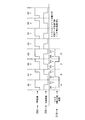
携帯電話または他の通信デバイス内のアプリケーションプロセッサ集積回路505およびモデムプロセッサ集積回路500を含むハイブリッド仮想GPIOアーキテクチャが図5に示されている。アプリケーションプロセッサ集積回路505用の送信ライン510aは、モデムプロセッサ集積回路500用の受信ラインである。同様に、モデムプロセッサ集積回路500用の送信ライン510bは、アプリケーションプロセッサ集積回路505用の受信ラインである。これらのラインまたはリードは、集積回路500と集積回路505との間の回路板または他の物理的相互接続上に担持される。各集積回路は、対応する送信ライン(たとえば、モデムプロセッサ集積回路500用のライン510b)に結合するための専用送信ピン512を含む。同様に、各集積回路は、対応する受信ライン(たとえば、モデムプロセッサ集積回路500用のライン510a)に結合するための専用受信ピン511を含む。各集積回路内のハイブリッド仮想有限状態機械(FSM)515は、本明細書でさらに説明するように、オーバーサンプリングクロック信号320(図3)のサイクルに関して、これらの専用ラインおよびピンを使用して送信および受信を制御する。
A hybrid virtual GPIO architecture that includes an application processor integrated
アプリケーションプロセッサ集積回路505は、プロセッサ502を含む。同様に、モデムプロセッサ集積回路500は、プロセッサ501を含む。各プロセッサは、従来の方法でGPIOピン525とインターフェースするGPIOインターフェース503を介して、GPIO信号を送信および受信する。各ハイブリッド仮想GPIOインターフェース503を介して処理された信号のある部分は、従来のGPIO信号530として、従来のGPIOピン525上で送信および受信され得る。しかし、GPIOインターフェース503を介して処理された信号の残りの部分は、従来のGPIOピン525を介して送信または受信されない。代わりに、この残りの信号部分の一部は、専用送信ピンおよび専用受信ピンを使用して対応するハイブリッド仮想FSM515を介して送信および受信される、複数の仮想GPIO信号535を備える。各ハイブリッド仮想FSM515はまた、メッセージング信号538を受信および送信することに関して、対応するプロセッサと直接インターフェースする。メッセージング信号538は、GPIO信号ではないので、GPIOインターフェース503を介して結合しない。各FSM515は、その専用の送信ピン512および受信ピン511を介して、メッセージング信号538を送信および受信する。したがって、これらのピンは、仮想GPIO信号535とメッセージング信号538の両方に使用されるという点で、「ハイブリッド」ピンである。
The application processor integrated
仮想GPIO信号535は各々、従来のGPIO信号530の場合のように、それら自体の専用ピンをもたない。これは、仮想GPIO信号535が各々、それら自体のピンを必要とするであろう従来のGPIO実施形態と比較して、結果として生じるハイブリッド仮想GPIOアーキテクチャがピンの著しい低減を達成するという点で、非常に有利である。メッセージング信号538は、従来であれば別の専用送信ピンおよび別の専用受信ピンも必要とする。しかし、本主題の有利なハイブリッド仮想GPIOアーキテクチャでは、これらの追加のピンも除去される。
Each
集積回路は、ただ1つのハイブリッド仮想FSM515を含み得るか、または複数の外部システムとインターフェースするための複数のこれらの要素を含み得る。図6Aは、集積回路600が、それ自体の単一のハイブリッド仮想FSM515を含む集積回路605内のリモートプロセッサと通信するための単一のハイブリッド仮想FSM515を含む、ハイブリッド仮想GPIOアーキテクチャを示す。対照的に、図6Bに示す集積回路620は、それぞれ集積回路625および630内のリモートプロセッサと通信するための第1のハイブリッド仮想FSM515Aおよび第2のハイブリッド仮想FSM515Bを含む。その点において、本明細書で説明する集積回路は、他のデバイスとシグナリングするハイブリッド仮想GPIOを適応させるのに必要なだけの数のハイブリッド仮想FSM515で構成され得る。
The integrated circuit may include only one hybrid virtual FSM515, or may include multiple of these elements for interfacing with multiple external systems. FIG. 6A shows a hybrid virtual GPIO architecture in which
再び図5を参照すると、仮想GPIO信号535はハイブリッド仮想FSM515などの有限状態機械を使用して適応されるので、プロセッサ501および502は、眠っているか、または別のタイプの休止状態であっても、仮想GPIO信号535およびメッセージング信号538を受信することが可能であり得る。このようにして、仮想GPIOアーキテクチャは、有利にはGPIOインターフェース503ごとのピンの数を節約するだけでなく、低電力でもある。
Seeing Figure 5 again, the
本明細書で使用する「ピン」は、集積回路が回路板または他の物理的相互接続(たとえば、パッケージ相互接続またはスルーホールビア相互接続)上のリードに結合するために使用するパッドまたは実際のピンなどの構造を包含する総称である。たとえば、図5に示すように各集積回路が16個のGPIOピンまたはパッド525を有する場合、これらのピンは、8つの対称GPIO信号530(説明を明快にするために、図5では4つの従来のGPIO信号#1〜#4のみが番号付けされている)または16個の非対称GPIO信号530を適応させるように構成され得る。加えて、各集積回路は、ライン510aおよび510bを使用して複数のm個の仮想GPIO信号535の入力/出力インターフェーシングを適応させることができ、mは任意の複数の整数である。同様に、各集積回路は、ライン510aおよび510bを使用して複数のM個のメッセージング信号538の入力/出力インターフェーシングを適応させることができ、Mは正の複数の整数である。各プロセッサコアに関して、GPIO信号530と仮想GPIO信号535との間に差はなく、これらの信号は両方とも、GPIOインターフェース503を介して必要に応じて送信および受信される信号であるにすぎない。しかしながら、従来のGPIO信号530とは対照的に、仮想GPIO信号535およびメッセージング信号538は専用ピンをもたないので、仮想GPIO信号535およびメッセージング信号538は、ライン510aおよび510b上で送信するためにハイブリッド仮想FSM515内で直列化される。受信されると、各ハイブリッド仮想FSM515は、受信された直列化仮想GPIO信号および受信された直列化メッセージング信号を非直列化する。したがって、各ハイブリッド仮想FSM515は、仮想GPIO信号535およびメッセージング信号538に関してシリアライザ/デシリアライザとして機能する。
As used herein, a "pin" is a pad or actual pad used by an integrated circuit to couple to leads on a circuit board or other physical interconnect (eg, package interconnect or through-hole via interconnect). It is a general term that includes structures such as pins. For example, if each integrated circuit has 16 GPIO pins or
プロセッサは、GPIO信号またはメッセージング信号のうちの選択された信号の変化に応答して、割込み信号を受信する必要がある場合がある。仮想GPIO信号535およびメッセージング信号538に関して、モデム電力マネージャ(MPM)540は、割込み構成レジスタ(図示せず)を介してプログラムされたように、選択されたGPIO信号またはメッセージング信号を監視する。各仮想GPIO信号535は、対応する割込み構成レジスタを有する。仮想GPIO信号535がその信号変化状態に応答して割込みを生成する必要がある場合、対応する構成レジスタは、それに応じてプログラムされる。同様に、仮想GPIO信号535またはメッセージング信号538が、その信号が状態を変化させたかどうかにかかわらず割込みを生成しない信号である場合、対応する割込み構成レジスタはやはり、それに応じてプログラムされる。MPM540は、有限状態機械を備える場合もある。したがって、ハイブリッド仮想FSM515とまったく同様に、MPM540は低電力であり、そのプロセッサがスリープモードまたは何らかの他の休止状態にあるかどうかにかかわらず、アクティブである。
The processor may need to receive an interrupt signal in response to changes in the selected signal of the GPIO or messaging signals. For
仮想GPIO信号535は、送信セットおよび受信セットに細分されてもよい。対称システムでは、各送信セットは、同じ数の信号を有することになる。同様に、各受信セットは、同じ数の信号を有することになる。しかしながら、開示する仮想GPIOアーキテクチャは、仮想GPIO信号535の送信セットおよびメッセージング信号538の送信セットが異なるサイズを有し、GPIO信号535の受信セットおよびメッセージング信号538の受信セットも異なるサイズを有する非対称シグナリング実施形態を容易に適応させることができるという点で、有利であることが諒解されよう。アーキテクチャが対称であるか非対称であるかにかかわらず、各ハイブリッド仮想FSM515は、これらの送信セット内の各信号がGPIOインターフェース503とハイブリッド仮想FSM515との間のそれ自体のリード上で搬送されるという意味では、GPIOインターフェース503から並列に仮想GPIO信号535の送信セットを受信する。メッセージング信号538はGPIO信号ではなく、したがって、GPIOインターフェース503を介して結合しない。代わりに、各プロセッサ501および502は、メッセージングレジスタ536のうちの対応するメッセージングレジスタからメッセージング信号538を取り出すか、またはそれらのメッセージングレジスタにメッセージング信号538を書き込む。メッセージング信号538の受信されたフレームに関して、対応するハイブリッド仮想FSMは、どのメッセージング信号538が特定のメッセージングレジスタに書き込まれたかを識別するために、フレーム中のビット順序を使用する。これらのメッセージングレジスタ536は各々、対応するプロセッサ501または502のためのアドレス空間内のハイブリッド仮想FSM515用の汎用アドレスのいくらかのオフセットにマッピングされる。したがって、各メッセージングレジスタ536は、それ自体のアドレス537を有する。MPM540からの割込みに応答して、プロセッサ501または502は次いで、適切なメッセージング信号538を取得するためにメッセージングレジスタ536にアクセスすることができる。仮想GPIO信号535とまったく同様に、メッセージング信号538は、送信セットおよび受信セットに細分され得る。アーキテクチャが対称であるか非対称であるかにかかわらず、ハイブリッド仮想FSM515によるこれらの送信セットの結果として生じる送信は、単一の送信ピン512を介して行われる。あるプロセッサからの仮想GPIO信号535の送信セットは、リモートプロセッサのための仮想GPIO信号535の受信セットになる。同様に、メッセージング信号538の送信セットは、リモートプロセッサのためのメッセージング信号538の受信セットになる。次いで、リモートプロセッサのハイブリッド仮想FSM515は、仮想GPIO信号535の受信セットを非直列化し、その結果、仮想GPIO信号535は、並列にGPIOインターフェース503に提示され得る。
The virtual GPIO signal 535 may be subdivided into transmit sets and receive sets. In a symmetric system, each transmission set will have the same number of signals. Similarly, each receive set will have the same number of signals. However, the disclosed virtual GPIO architecture is asymmetric signaling in which the transmit set of
各ハイブリッド仮想FSM515は、仮想GPIO信号535の送信セットおよびメッセージング信号538の送信セットについての以前の状態を記憶する構成レジスタ(図示せず)を含む。このようにして、各ハイブリッド仮想FSM515は、GPIOインターフェース503から受信された仮想GPIO信号535の送信セットの現在の状態を監視し、現在の状態が以前の状態に対して変化した場合のみ、対応する送信セットの直列送信をトリガすることができる。言い換えれば、ハイブリッド仮想FSM515は、送信セット内の信号のうちの1つまたは複数が、構成レジスタ内の以前の状態の記憶を介して検出されるように状態を変化させた場合のみ、メッセージング信号538または仮想GPIO信号535の送信セットの直列送信をトリガする。各プロセッサは、メッセージング信号レジスタ536用のアドレス537を知っており、したがって、それらに所望の送信セットを書き込むことができ、受信セットの任意の変化を読み取ることもできる。ハイブリッド仮想FSM515は、メッセージング信号536の送信セットがそれらの以前の送信に対して変化したかどうかを監視し、それに応じてリモートプロセッサへの送信セットの送信をトリガする。MPM540は、受信セットが以前に説明したように変化したかどうかを監視し、変化した受信セットが処理され得るように対応するプロセッサに割り込む。
Each hybrid virtual FSM515 includes a configuration register (not shown) that stores previous states for the transmit set of
送信されたフレームおよび受信されたフレームは、事前定義されたサイズを有する。フレームサイズのこの事前定義は、ハイブリッド仮想FSM515が、受信された仮想GPIO信号535および受信されたメッセージング信号538をフレーム内のそれらの順序によって識別するという点で、必要である。送信プロセッサが、デフォルトのフレームサイズに含まれ得るよりも多くの仮想GPIO信号535またはメッセージング信号538を送信する必要がある場合、送信ハイブリッド仮想FSM515は、そのフレームサイズをデフォルトの長さから新しいプログラムされた長さに変更するために、受信ハイブリッド仮想FSM515にシグナリングし得る。たとえば、フレームサイズは、一定数のビット長になるようにヘッダによってプログラムされ得る。例示的なフレーム700が図7に示されている。ヘッダ705は、2つのファンクションビット、fn_0およびfn_1を備え得る。一実施形態では、両方のファンクションビットが0である場合、後続のビットは仮想GPIO信号535である。fn_0が0であり、fn_1が1に等しい場合、後続のビットはメッセージング信号538である。fn_0が1であり、fn_1が0に等しい場合、フレームペイロード内の後続のビットは、受信ハイブリッド仮想FSM515によって予想されることになる新しい仮想GPIO(またはメッセージング信号)フレーム長を表す。同様に、両方のファンクションビットが1である場合、後続のビットは、リモートプロセッサによる所望のフレーム長の確認を表す。仮想GPIO信号535の送信セット(またはメッセージング信号538の送信セット)がこの固定フレームサイズ未満である場合、各フレーム内の未使用ビットはドントケア値であり得る。代替的に、各ハイブリッド仮想FSM515は、所与のアプリケーションに必要なビットの数に応じて、送信されるフレームのサイズを変更するように構成され得る。2つのファンクションビットを使用するコーディングの前述の説明は一例にすぎず、他のヘッダおよびコーディングプロトコルは、フレームが、仮想GPIO信号535、メッセージング信号538、仮想GPIOフレーム長の識別情報、仮想GPIOフレーム長の確認、メッセージング信号フレーム長の識別情報、またはメッセージング信号フレーム長の確認を搬送しているかどうかを識別するために使用され得ることが諒解されよう。一実施形態では、フレーム700は、フレームペイロードが仮想GPIO信号535を備えるかまたはメッセージング信号538を備えるかを識別するタイプビット(type_bit)も含み得る。
The transmitted frame and the received frame have a predefined size. This predefinition of frame size is necessary in that the hybrid virtual FSM515 identifies the received
仮想GPIO信号535またはメッセージング信号538の受信セットのための完全なフレームの受信を検出するために、ハイブリッド仮想FSM515は、フレーム700のスタートビット706の受信後オーバーサンプリングクロック320(図3)の必要なサイクル数をカウントする論理回路(図示せず)を含み得る。たとえば、受信セットが、オーバーサンプリングクロック320の100サイクル(10Xオーバーサンプリングレート)に応答して受信される10個の仮想GPIO信号535を備えると仮定する。スタートビット706を検出し、オーバーサンプリングクロック320の別の100サイクルを待機した後、FSM論理回路は、次いで、エンドビット710の受信を期待することになる。
To detect the reception of a complete frame for the receive set of virtual GPIO signal 535 or
再び図7を参照すると、仮想GPIO信号の送信セットは、したがって、スタートビット706およびエンドビット710によって画定されたフレーム700中で送信される。送信プロセッサのための送信セットはリモートプロセッサのための受信セットになるので、受信セットも、それに応じてフレーム化される。このフレーム化は、その場合、各プロセッサが、いかなる追加の専用ピンも必要とせずにリモートプロセッサの健全性を監視することができるという点で、有利である。たとえば、各ハイブリッド仮想FSM515は、(仮想GPIO信号の送信セットについての以前の状態に対する現在の状態に変化がない)デフォルト状態の間、その専用送信ピン512を電源電圧に弱く引く(したがって、その送信ライン510aを電源電圧に弱く引く)ように構成され得る。スタートビットは、そのような実施形態の場合、ハイブリッド仮想FSM515がスタートビット706の送信のためにその送信ライン510aを接地するような論理0になる。このようにして、各ハイブリッド仮想FSM515は、その受信ライン510bが接地に向かって引かれたことを検出することによって、スタートビット706の受信を容易に検出することができる。一実施形態では、スタートビット706およびストップビット710は、互いの論理補数である。したがって、スタートビット706が論理0である場合、ストップビット710は論理高値になる。次いで、フレーム700のペイロードは、タイプビットから、フレーム終了を画定するストップビット710まで拡張してもよい。
Referring again to FIG. 7, the transmission set of virtual GPIO signals is therefore transmitted in
プロセッサが失敗し、その結果、その送信ライン510aを接地に不適切に引く可能性がある。したがって、リモートハイブリッド仮想FSM515は、スタートビット706としてこれを検出することになり、その論理回路は、それに応じてフレーム700の終わりに向かってカウントを開始することになる。しかし、エンドビット710が論理1である場合、各ハイブリッド仮想FSM515は、フレーム送信の終わりをシグナリングするために、その送信ライン510aを電源電圧に充電する。プロセッサが失敗し、その結果、リモートハイブリッド仮想FSM515がスタートビット706であると見なされるものを検出した場合、論理回路はエンドビットを検出せず、それに応じて、そのプロセッサにリモートプロセッサの失敗を通知する。
The processor may fail, resulting in improperly pulling its transmit
開示する仮想ハイブリッドGPIOアーキテクチャの利点を考えると、2つのピンのみが必要であるが、任意の数の仮想GPIO信号535およびメッセージング信号538がハイブリッド仮想有限状態機械515を介して直列化および非直列化され得る。唯一の制限は、オーバーサンプリングクロック320およびクロックの遅れまたは進みの任意の予想量に対する仮想GPIO信号のタイミング要件である。さらに、あるプロセッサの健全性を対向するプロセッサに対してトランスペアレントにするために、他のピンが必要になることはない。フレーム700はまた、わずか2つのファンクションビットのオーバーヘッドだけによって、様々なメッセージング信号538および仮想GPIO信号535が専用送信ピン112を介して送信され得るという点で、非常に有利である。
Given the benefits of the disclosed virtual hybrid GPIO architecture, only two pins are needed, but any number of virtual GPIO signals 535 and
各ハイブリッド仮想FSM515は、図3および図4に関して説明したように、シンボル100、105、110、および115に関して説明したものなどのマルチモード変調を使用してフレーム700を送信および受信するように構成され得る。各受信されたシンボルは、そのオーバーサンプリングクロックを使用して受信されたシンボルをサンプリングし、バイナリ1サンプルの結果として生じる数をバイナリ0サンプルに対して比較することによって、受信ハイブリッド仮想FSM515によって変調され得る。
Each hybrid virtual FSM515 is configured to transmit and receive
図8は、その送信動作および受信動作をより良く示す、マルチモード変調ハイブリッド仮想FSM515のブロック図である。FSM515は、多重化モジュール800を介して、(図5に示す)そのGPIOインターフェース503から仮想GPIO信号535の送信セットを受信する。代替的に、多重化モジュール800は、FSM515に関して前に説明したように、メッセージング信号538の送信セットを受信してもよい。FSM515は、送信セットの以前の状態と比較して送信セットに変化があった場合、送信ライン510aを介したマルチモード変調シンボルとしての信号の送信セットの直列送信を許可する論理回路801を含む。このようにして、以前の送信と比較して状態が変化していない送信セットの不要な再送信はない。したがって、論理回路801は、仮想GPIO信号535の現在の送信セットを、ラッチまたは構成レジスタ807に記憶された以前の送信セットと比較する。比較を実行するために、論理回路801は、現在の送信セットを構成レジスタ807に記憶された以前の送信セットとXORするXORゲート810を含み得る。多重化モジュール800は、並列入力直列出力(PISO)シフトレジスタ815の中に並列に現在の送信セットをロードする。XORゲート810からのイネーブル信号820が高くなった(現在の送信セットと構成レジスタ807に記憶された送信セットとの間の変化を示す)場合、PISOシフトレジスタ815はイネーブルにされて、シフトクロック120に応答して、そのコンテンツを送信ライン510a上に直列にシフトアウトする。
FIG. 8 is a block diagram of the multimode modulation hybrid virtual FSM515 showing its transmit and receive operations better. The FSM515 receives a transmission set of virtual GPIO signals 535 from its GPIO interface 503 (shown in FIG. 5) via the
信号の各送信セットは、PISOシフトレジスタ815に記憶されたデータのフレームを備える。FSM515は、PISOシフトレジスタ815からシフトアウトされたビットの送信セットを、送信ライン510a上のリモートプロセッサに駆動されるマルチモード変調シンボルにマルチモード変調する、マルチモード変調器855を含む。この変調は、オーバーサンプリングクロックソース861からのオーバーサンプリングクロック信号320のカウントなどの、発振器からの発振サイクルのカウントに応答する。変調器855およびオーバーサンプリングクロックソース861は、XORゲート810からのイネーブル信号820のアサーションによってトリガされ得る。このトリガに応答して、変調器855は、PISOシフトレジスタ815が信号の送信セットからのビットの初期ペアを変調器855にシフトするように、シフト信号120をストローブする。たとえば、シフトクロック120は、オーバーサンプリングクロック320の周波数をそのオーバーサンプリングレートだけ減少させることによって、オーバーサンプリングクロック320から導出され得る。
Each transmission set of signals comprises a frame of data stored in the
このようにして、PISOシフトレジスタ815に記憶されたデータのフレームのための信号の送信セットは、一度にビットのペアを変調器855にシフトされる。PISOシフトレジスタ815からシフトアウトされたペア内の各ビットのバイナリ値に応じて、マルチモード変調器855は、送信ライン510aを介して送信された対応するシンボルをパルス幅変調および位相変調する。その点において、各プロセッサは、デフォルト状態(データ送信なし)の間、その送信ライン510aを電源電圧VDDまで高に弱く充電するように構成され得る。再び図3を参照すると、変調器855は変調器310を備え得る。
In this way, the transmission set of signals for a frame of data stored in the
FSM515はまた、直列入力並列出力(SIPO)シフトレジスタ825を使用して、類似する方法で信号(仮想GPIO信号535および/またはメッセージング信号538)の受信セットを非直列化する。マルチモード復調器870は、受信ライン510b上で受信された、リモートプロセッサから受信されたマルチモード変調シンボルを復調する。フレームごとのスタートビットは、オーバーサンプリングクロック875からのオーバーサンプリングクロック信号880を同期させるために使用される。代替実施形態では、クロック875および861は同じクロックを備え得ることに留意されたい。復調器870はまた、フレーム全体が受信されたことを検出すると、シフト信号881をSIPOシフトレジスタ825にアサートしてもよい。次いで、SIPOシフトレジスタ825は、復調器870からの復調データ信号882をシフトインすることになる。フレームが受信されると、フレームは出力ラッチ851においてラッチされ、その結果、フレームは並列に多重化モジュール800に提示され得る。
The FSM515 also uses the serial input parallel output (SIPO)
図7に関して説明したファンクションビットは、誤り訂正コーディングによって向上し得る。誤り訂正コーディングはレイテンシを増加させるが、その場合、ファンクションビットは、誤り訂正コーディングによって訂正され得るビット誤りの影響を受けない。ひいては、ユーザは、肯定応答(ACK)および否定応答(NACK)などの重要なファンクションヘッダが誤りなしで配信されることを確信することができる。以下の実施形態は、固有の機能を定義するための拡張ハミング(8,4)コードワードの使用を対象とするが、他の誤り訂正技法が使用されてもよいことが諒解されよう。 The function bits described with respect to FIG. 7 can be improved by error correction coding. Error correction coding increases latency, in which case the function bits are unaffected by bit errors that can be corrected by error correction coding. As a result, the user can be confident that important function headers such as acknowledgments (ACKs) and negative responses (NACKs) will be delivered without error. The following embodiments cover the use of extended humming (8,4) codewords to define unique functionality, but it will be appreciated that other error correction techniques may be used.
誤り訂正を伴う例示的なフレーム900が図9に示されている。フレーム700に類似して、フレーム900はスタートシンボルで始まり、論理高(VDDにアサートされた)ストップシンボルで終わる。10ビット長のファンクションビットフィールド905は、たとえば、最大128データビットのデータペイロード910に関連付けられたメタデータを提供する。これらのデータビットは、図7に関して説明したように、仮想GPIO信号530および/またはメッセージング信号538を備え得る。ファンクションビットフィールド905とデータペイロード910の両方は、マルチモード変調シンボルとして送信される。たとえば、第1のシンボル915は、動作モードビットD0と動作モードビットD1の両方を表す。2つの動作モードビットが存在するので、これらの動作モードビットは、4つの異なる動作モードについて符号化する。第1の動作モードは、フレーム1100についての図10に示すように、両方とも0に等しい動作モードビットD0および動作モードビットD1に対応する。このモードでは、データペイロード910は、固定サイズの8つの仮想GPIOビット535を有する。この固定フレームサイズおよび比較的短いデータペイロード1010を考慮すれば、ファンクションビットフィールド905は、この第1の動作モードにおいて、2つの動作モードビットD0および動作モードビットD1だけに短縮され得る。
An
第2および第3の動作モードは、図11に示すフレーム1100に対応する。動作モードビットD0が1に等しく、動作モードビットD1が0に等しい場合、第1のP2P(ポイントツーポイント)メッセージング方式が使用される。この第1のP2Pメッセージング方式では、動作モードビットD0および動作モードビットD1の後に8ビット機能フィールドが続く。8ビット機能フィールドは、図12に示すハミングコードワードを形成し得る。このようにして、8ビット機能フィールドは誤りに対してロバストになり、その結果、受信ハイブリッド仮想FSMは、送信されているタイプのフレームをロバストに復号することができる。8つのビットが存在するので、図12に示すように、送信され得る16個のハミングコードワードが存在する。一実施形態では、ファンクションヘッダコードワードは、ビット反転したペアを形成して、結果として生じる復号を有利に簡略化することができる。たとえば、コードワード6は、ポイントツーマルチポイントネットワークに対するアドレス指定されたACKであるが、ビット反転したコードワード9はアドレス指定されたNACKである。同様に、コードワード7はダイレクトACK(ポイントツーポイントネットワーク)であるが、ビット反転したコードワード8はダイレクトNACKである。コードワード5およびそのビット反転した対応するコードワード10は、将来使うために予約され得る。コードワード4は、アドレス指定されたネットワークに対するフロー制御オーバーライドメッセージ(FCOM:flow control override message)を指定する。対応するビット反転したコードワード11は、ダイレクトネットワークに対するフロー制御オーバーライドメッセージである。コードワード3は、関連するデータペイロードをアドレス指定されたネットワークのためのメッセージングペイロードであるものとして識別するが、対応するビット反転したコードワード12は、関連するデータペイロードがダイレクトネットワークのためのメッセージングペイロードであることを示す。コードワード2は、関連するデータペイロードがアドレス指定されたネットワークのための仮想GPIOペイロードであることを示すが、ビット反転したコードワード13は、関連するデータペイロードがダイレクトネットワークのための仮想GPIOペイロードであることを示す。コードワード1は、フレームがブロードキャストフレームであることを意味するが、ビット反転したコードワード14は、フレームがリッスン専用クエリであることを意味する。最後に、コードワード0はソフトリセットをトリガするが、対応するビット反転したコードワード15は最低速度動作モードをトリガする。図12のコードワードの割当ては一実施形態を示すものにすぎず、多数の代替コードワード割当てが利用されてもよいことが諒解されよう。
The second and third operating modes correspond to frame 1100 shown in FIG. If the operating mode bit D0 is equal to 1 and the operating mode bit D1 is equal to 0, then the first P2P (point-to-point) messaging scheme is used. In this first P2P messaging scheme, the operating mode bit D0 and the operating mode bit D1 are followed by an 8-bit functional field. The 8-bit functional field can form the Hamming code word shown in FIG. In this way, the 8-bit functional field becomes robust to errors, so that the receive hybrid virtual FSM can robustly decode the type of frame being transmitted. Since there are 8 bits, there are 16 Hamming code words that can be transmitted, as shown in Figure 12. In one embodiment, the function header codewords can form bit-inverted pairs to advantageously simplify the resulting decoding. For example, codeword 6 is an addressed ACK for a point-to-multipoint network, while bit-inverted codeword 9 is an addressed NACK. Similarly,
再び図11を参照すると、第3の動作モードは、0に等しい動作モードビットD0および1に等しい動作モードビットD1に対応する。この動作モードでは、動作モードビットに続くファンクションビットフィールドは、0ビットから8ビットにわたることがある。これらのファンクションビットは、図12に示すコードワードのうちの選択されたコードワードに任意に割り当てられ得る。 With reference to FIG. 11 again, the third mode of operation corresponds to the mode of operation bit D0 equal to 0 and the mode bit D1 equal to 1. In this mode of operation, the function bit field following the mode of operation bits can range from 0 bits to 8 bits. These function bits can be arbitrarily assigned to the selected codeword of the codewords shown in FIG.
第4の動作モードは、第1のシンボル915内の動作モードビットD0と動作モードビットD1の両方が1に等しい、図13に示すフレーム1300に対応する。このモードでは、動作モードビットに続くシンボルは、図7に関して説明したファンクションビットD0およびファンクションビットD1 705を備える。したがって、この第4の動作モードは、メッセージング信号および仮想GPIO信号のペイロードに使用されるべき新しい仮想GPIOストリーム長のプログラミングをサポートする。
The fourth mode of operation corresponds to frame 1300 shown in FIG. 13, in which both the mode of operation bit D0 and the mode of operation bit D1 in the
フレーム900、1000、1100、および1300のペイロードはすべて、誤り訂正のためにも符号化され得ることに留意されたい。加えて、これらのフレームの各々は、シンボル周期にわたる同期シンボル(クロック同期)で始まる。クロック同期シンボルの前半では、送信ハイブリッド仮想FSM515はその送信ピンを充電する。同期シンボルの後半では、送信ハイブリッド仮想FSM515はその送信ピンを電源電圧VDDに戻して充電する。送信ピンのデフォルト状態が高であるので、受信ハイブリッド仮想FSM515は、同期シンボルの前半を受信すると、その受信ピンの充電を容易に検出することができる。受信ハイブリッド仮想FSM515は、シンボル送信の中間点における同期シンボルの立上りエッジを容易に検出することもできる。したがって、受信FSMは、同期シンボルのこの立上りエッジに応答して、そのオーバーサンプリングクロックを同期させることができる。
Note that the payloads of
次に、第1の動作方法について、図14Aのフローチャートに関して説明する。第1の方法は、GPIOインターフェースにおいて、GPIO信号の送信セットを受信する行為1400を含む。対応するプロセッサ501または502からのGPIOインターフェース503におけるGPIO信号の送信セットの受信は、行為1400の一例である。方法は、GPIOインターフェースから、GPIOピンを介してGPIO信号の第1の部分を送信する行為1405も含む。GPIOピン525のうちの対応するGPIOピンを介したGPIO信号530の送信は、行為1405の一例である。加えて、方法は、GPIOインターフェースから、GPIO信号の第2の部分を有限状態機械(FSM)に送信する行為1410を含み、GPIO信号の第2の部分は、一連のビットペアに配置される。変調器855におけるビットペアの受信は、行為1410の一例である。以下の行為は、各ビットペアに関して定義される。行為1415は、ビットペアにおける第1のビットに基づいており、選択されたパルス幅を提供するために、少なくとも2つのパルス幅から選択することを備える。ルックアップテーブル328に関して説明した、各ビットペアにおける位相幅ビットに基づいたパルス幅の選択は、行為1415の一例である。行為1420は、ビットペアにおける第2のビットに基づいており、選択されたエッジ整合を提供するために、シンボル周期の始めとの選択されたパルス幅の立上りエッジ整合、およびシンボル周期の終わりとの選択されたパルス幅の立下りエッジ整合から選択することを備える。ルックアップテーブル328に関して説明した、各ビットペアにおける位相制御ビットによる位相の制御は、行為1420の一例である。最後に、方法は、FSMから、選択されたパルス幅および選択されたエッジ整合に従ってシンボル周期内に送信ピンを介してパルスを送信する行為1425を含み、パルスは、選択されたパルス幅の間は電源電圧に等しく、選択されたパルス幅以外では接地に等しい。変調器855によるパルス幅変調位相幅変調シンボルの送信は、行為1425の一例である。
Next, the first operation method will be described with respect to the flowchart of FIG. 14A. The first method involves receiving an
第2の動作方法について、図14Bのフローチャートに関して説明する。行為1430および行為1435は、それぞれ、行為1400および行為1405に類似している。方法は、専用送信ピンを介してGPIO信号のセットの残りの部分を第1のフレーム中で仮想GPIO信号としてリモートプロセッサに直列送信する行為1440も含み、各第1のフレームは、第1のフレームを仮想GPIOフレームとして識別する第1のヘッダを含み、第1のヘッダは誤り訂正コーディングされる。最後に、方法は、メッセージング信号レジスタから第1のプロセッサによって書き込まれたメッセージング信号を取り出し、取り出されたメッセージング信号を専用送信ピンを介して第2のフレーム中でリモートプロセッサに直列送信する行為1445を含み、各第2のフレームは、第2のフレームをメッセージングフレームとして識別する第2のヘッダを含み、第2のヘッダは誤り訂正コーディングされる。
The second operation method will be described with respect to the flowchart of FIG. 14B.
本明細書で開示するハイブリッド仮想GPIOインターフェース(図示せず)を介して複数の周辺デバイス1510と通信するように構成されたシステムオンチップ(SoC)1505を含む例示的なシステム1500が図15に示されている。したがって、各周辺デバイス1510は、本明細書で開示するハイブリッド仮想FSM(図示せず)も含む。システム1500は、セルラーフォン、スマートフォン、携帯情報端末、タブレットコンピュータ、ラップトップコンピュータ、デジタルカメラ、ハンドヘルドゲームデバイス、または他の適切なデバイスを備え得る。メッセージング信号および仮想GPIO信号を周辺デバイス1510に送信するためにそのハイブリッド仮想FSMを使用することに加えて、SoC1505は、DRAM1520などのメモリおよびディスプレイコントローラ1525にも結合するシステムバス1515を介して通信する。ディスプレイコントローラ1525は、ディスプレイ1535を駆動するビデオプロセッサ1530に結合する。
An
今では当業者が諒解するように、目下の特定の適用例に応じて、本開示のデバイスの材料、装置、構成および使用方法において、また、それらに対して、本開示の範囲から逸脱することなく、多くの修正、置換および変形が行われ得る。このことに照らして、本明細書において図示および説明した特定の実施形態は本開示のいくつかの例としてのものにすぎないので、本開示の範囲はそれらの特定の実施形態の範囲に限定されるべきではなく、むしろ、以下に添付された特許請求の範囲およびそれらの機能的等価物の範囲と完全に相応すべきである。 As will now be appreciated by those skilled in the art, in the materials, devices, configurations and uses of the devices of the present disclosure, and for them, deviating from the scope of the present disclosure, depending on the particular application at present. Many modifications, replacements and modifications can be made without it. In light of this, the scope of the present disclosure is limited to the scope of those particular embodiments, as the particular embodiments illustrated and described herein are merely examples of the present disclosure. Rather, it should be in full agreement with the claims and their functional equivalents attached below.
100 第1のパルス、パルス、出力ワード、ワード、シンボル
105 残りのパルス、パルス、出力ワード、ワード、シンボル
110 パルス、出力ワード、ワード、シンボル
115 パルス、出力ワード、ワード、シンボル
120 シフトクロック、シフト信号
200 パルス幅変調シーケンス、シーケンス、変調シーケンス
205 位相変調シーケンス、シーケンス、変調シーケンス
210 マルチ変調シーケンス、シーケンス
300 送信機
305 ビットデマルチプレクサ、デマルチプレクサ
310 変調器
315 出力ピン
320 オーバーサンプリングクロック信号、オーバーサンプリングクロック
325 出力ドライバ
326 インバータ
328 4ビットルックアップテーブル、ルックアップテーブル
400 オーバーサンプリングクロック信号
500 モデムプロセッサ集積回路、集積回路
501 プロセッサ
502 プロセッサ
503 GPIOインターフェース、ハイブリッド仮想GPIOインターフェース
505 アプリケーションプロセッサ集積回路、集積回路
510a 送信ライン、ライン
510b 送信ライン、ライン、受信ライン
511 専用受信ピン、受信ピン
512 専用送信ピン、送信ピン
515 ハイブリッド仮想FSM、リモートハイブリッド仮想FSM、ハイブリッド仮想有限状態機械、送信ハイブリッド仮想FSM、受信ハイブリッド仮想FSM、マルチモード変調ハイブリッド仮想FSM、FSM
515A 第1のハイブリッド仮想FSM
515B 第2のハイブリッド仮想FSM
525 GPIOピン、パッド
530 GPIO信号、対称GPIO信号、非対称GPIO信号、仮想GPIO信号
535 仮想GPIO信号、GPIO信号
536 メッセージングレジスタ、メッセージング信号レジスタ、メッセージング信号
537 アドレス
538 メッセージング信号
540 モデム電力マネージャ(MPM)、MPM
600 集積回路
605 集積回路
620 集積回路
625 集積回路
630 集積回路
700 フレーム
705 ヘッダ、ファンクションビットD0およびファンクションビットD1
706 スタートビット
710 エンドビット、ストップビット
800 多重化モジュール
801 論理回路
807 構成レジスタ
810 XORゲート
815 並列入力直列出力(PISO)シフトレジスタ、PISOシフトレジスタ
820 イネーブル信号
825 直列入力並列出力(SIPO)シフトレジスタ、SIPOシフトレジスタ
851 出力ラッチ
855 マルチモード変調器、変調器
861 オーバーサンプリングクロックソース、クロック
870 マルチモード復調器、復調器
875 オーバーサンプリングクロック、クロック
880 オーバーサンプリングクロック信号
881 シフト信号
882 復調データ信号
900 フレーム
905 ファンクションビットフィールド
910 データペイロード
915 第1のシンボル
1000 フレーム
1010 データペイロード
1100 フレーム
1300 フレーム
1500 システム
1505 システムオンチップ(SoC)、SoC
1510 周辺デバイス
1515 システムバス
1520 DRAM
1525 ディスプレイコントローラ
1530 ビデオプロセッサ
1535 ディスプレイ
100 1st pulse, pulse, output word, word, symbol
105 Remaining pulses, pulses, output words, words, symbols
110 pulses, output words, words, symbols
115 pulses, output words, words, symbols
120 shift clock, shift signal
200 pulse width modulation sequence, sequence, modulation sequence
205 Phase Modulation Sequence, Sequence, Modulation Sequence
210 Multi-modulation sequence, sequence
300 transmitter
305-bit demultiplexer, demultiplexer
310 modulator
315 output pin
320 oversampling clock signal, oversampling clock
325 output driver
326 Inverter
328 4-bit look-up table, look-up table
400 oversampling clock signal
500 modem processor integrated circuit, integrated circuit
501 processor
502 processor
503 GPIO interface, hybrid virtual GPIO interface
505 Application Processor Integrated Circuits, Integrated Circuits
510a transmit line, line
510b transmit line, line, receive line
511 Dedicated receive pin, receive pin
512 Dedicated transmit pin, transmit pin
515 Hybrid Virtual FSM, Remote Hybrid Virtual FSM, Hybrid Virtual Finite State Machine, Transmit Hybrid Virtual FSM, Receive Hybrid Virtual FSM, Multimode Modulation Hybrid Virtual FSM, FSM
515A First Hybrid Virtual FSM
515B Second hybrid virtual FSM
525 GPIO pins, pads
530 GPIO signal, symmetric GPIO signal, asymmetric GPIO signal, virtual GPIO signal
535 Virtual GPIO signal, GPIO signal
536 messaging registers, messaging signal registers, messaging signals
537 address
538 Messaging signal
540 Modem Power Manager (MPM), MPM
600 integrated circuit
605 integrated circuit
620 integrated circuit
625 integrated circuit
630 integrated circuit
700 frames
705 Header, Function Bit D0 and Function Bit D1
706 Start bit
710 end bit, stop bit
800 multiplexing module
801 logic circuit
807 configuration register
810 XOR gate
815 Parallel Input Series Output (PISO) Shift Register, PISO Shift Register
820 enable signal
825 Series Input Parallel Output (SIPO) Shift Register, SIPO Shift Register
851 Output latch
855 Multimode modulator, modulator
861 Oversampling clock source, clock
870 Multimode demodulator, demodulator
875 Oversampling clock, clock
880 oversampling clock signal
881 shift signal
882 Demodulated data signal
900 frames
905 function bit field
910 data payload
915 First symbol
1000 frames
1010 data payload
1100 frame
1300 frame
1500 system
1505 System on Chip (SoC), SoC
1510 peripheral devices
1515 system bus
1520 DRAM
1525 display controller
1530 video processor
1535 display
Claims (15)
前記GPIOインターフェースから、GPIOピンを介して前記GPIO信号の第1の部分を送信するステップと、
前記GPIOインターフェースから、前記GPIO信号の第2の部分を有限状態機械(FSM)に供給するステップであって、前記GPIO信号の前記第2の部分が、一連のビットペアに配置される、ステップと、
前記FSMにおいて受信されたビットペアごとに、
前記ビットペアにおける第1のビットに基づいて、選択されたパルス幅を提供するために、少なくとも2つの異なるパルス幅から選択するステップと、
前記ビットペアにおける第2のビットに基づいて、選択されたエッジ整合を提供するために、シンボル周期の始めとの前記選択されたパルス幅の立上りエッジ整合、および前記シンボル周期の終わりとの前記選択されたパルス幅の立下りエッジ整合から選択するステップと、
前記選択されたパルス幅および前記選択されたエッジ整合に従って、前記シンボル周期内に送信ピンを介して仮想GPIOパルスを送信するステップであって、前記仮想GPIOパルスが、前記選択されたパルス幅の間は電源電圧に等しく、前記選択されたパルス幅以外では接地に等しい、ステップと
を備える方法。 In the GPIO interface, the step of receiving the transmission set of GPIO signals,
The step of transmitting the first part of the GPIO signal from the GPIO interface via the GPIO pin, and
A step of supplying a second portion of the GPIO signal from the GPIO interface to a finite state machine (FSM), wherein the second portion of the GPIO signal is arranged in a series of bit pairs.
For each bit pair received in the FSM
A step of selecting from at least two different pulse widths to provide a selected pulse width based on the first bit in the bit pair.
The rising edge matching of the selected pulse width with the beginning of the symbol period and the selection with the end of the symbol period to provide the selected edge matching based on the second bit in the bit pair. Steps to select from falling edge matching of pulse width and
A step of transmitting a virtual GPIO pulse through a transmit pin within the symbol period according to the selected pulse width and the selected edge matching, wherein the virtual GPIO pulse is between the selected pulse widths. Is equal to the power supply voltage and equal to ground except for the selected pulse width, with steps.
前記FSMにおいて、前記複数のメッセージング信号を前記対応する複数のメッセージングレジスタから取り出すステップであって、前記取り出された複数のメッセージング信号が、一連のビットペアに配置される、ステップと、
前記FSMにおいて取り出された前記複数のメッセージング信号のビットペアごとに、
前記複数のメッセージング信号のビットペアにおける第1のビットに基づいて、選択されたパルス幅を提供するために、少なくとも前記2つのパルス幅から選択するステップと、
前記複数のメッセージング信号のビットペアにおける第2のビットに基づいて、選択されたエッジ整合を提供するために、前記シンボル周期の前記始めとの前記選択されたパルス幅の立上りエッジ整合、および前記シンボル周期の前記終わりとの前記選択されたパルス幅の立下りエッジ整合から選択するステップと、
前記選択されたパルス幅および前記選択されたエッジ整合に従って、前記シンボル周期内に前記送信ピンを介してメッセージング信号パルスを送信するステップであって、前記メッセージング信号パルスが、前記選択されたパルス幅の間は前記電源電圧に等しく、前記選択されたパルス幅以外では前記接地に等しい、ステップと
をさらに備える、請求項1に記載の方法。 The steps from the processor to write multiple messaging signals to the corresponding multiple messaging registers,
In the FSM, a step of extracting the plurality of messaging signals from the plurality of corresponding messaging registers, wherein the plurality of extracted messaging signals are arranged in a series of bit pairs.
For each bit pair of the plurality of messaging signals extracted in the FSM,
A step of selecting from at least the two pulse widths to provide a selected pulse width based on the first bit in the bit pair of the plurality of messaging signals.
Rising edge matching of the selected pulse width with said beginning of said symbol period, and said symbol period to provide selected edge matching based on the second bit in the bit pair of the plurality of messaging signals. With the step of selecting from the falling edge matching of the selected pulse width with the end of the
A step of transmitting a messaging signal pulse through the transmit pin within the symbol period according to the selected pulse width and the selected edge matching, wherein the messaging signal pulse is of the selected pulse width. The method of claim 1, further comprising a step equal to the power supply voltage and equal to the ground except for the selected pulse width.
各受信されたメッセージング信号パルスを、前記受信されたメッセージング信号パルスの前記到着順序に従って選択された対応する受信メッセージングレジスタに書き込むステップと
をさらに備え、
前記リモート集積回路内のプロセッサにおいて、前記受信されたメッセージング信号パルスを前記対応する受信メッセージングレジスタから取り出すステップをさらに備える、請求項4に記載の方法。 A step of receiving each messaging signal pulse via a receive pin in a remote integrated circuit, wherein the messaging signal pulse has an arrival order at the receive pin.
It further comprises writing each received messaging signal pulse to a corresponding received messaging register selected according to said arrival order of said received messaging signal pulse.
The method of claim 4, further comprising taking the received messaging signal pulse from the corresponding received messaging register in the processor in the remote integrated circuit.
各受信された仮想GPIOパルスから前記GPIO信号の前記ビットペアを復元するために、そのパルス幅に応答して、また、前記立上りエッジ整合を有するかまたは前記立下りエッジ整合を有するかに応答して、各受信された仮想GPIOパルスを復調するステップと
をさらに備える、請求項1に記載の方法。 The step of receiving the virtual GPIO pulse via the receive pin in the remote integrated circuit,
To restore the bit pairs of the GPIO signals from each received virtual GPIO pulses, in response to the pulse width, also, in response to whether or has the falling edge aligned with the rising edge matching The method of claim 1, further comprising demodulating each received virtual GPIO pulse.
前記複数のGPIOピンを介してGPIO信号の送信セットの第1の部分を送信するように構成されたGPIOインターフェースと、
送信ピンと、
前記GPIOインターフェースから前記GPIO信号の送信セットの第2の部分を受信するように構成された有限状態機械(FSM)であって、前記第2の部分が、一連のビットペアに配置され、前記FSMが、ビットペアにおける第1のビットに対応する第1のパルス幅および異なる第2のパルス幅から選択されたパルス幅を有し、前記ビットペアにおける第2のビットに対応する位相変調を有する前記ビットペアごとに仮想GPIOシンボルを形成するようにさらに構成され、前記FSMが、前記送信ピンを介して前記仮想GPIOシンボルを送信するようにさらに構成される、FSMと
を備える集積回路。 With multiple GPIO pins,
With a GPIO interface configured to transmit the first part of the transmission set of GPIO signals through the multiple GPIO pins,
Send pin and
A finite state machine (FSM) configured to receive a second portion of the GPIO signal transmission set from the GPIO interface, the second portion being arranged in a series of bit pairs, the FSM For each bit pair having a first pulse width corresponding to the first bit in the bit pair and a pulse width selected from a different second pulse width and having a phase modulation corresponding to the second bit in the bit pair. An integrated circuit comprising an FSM that is further configured to form a virtual GPIO symbol and the FSM is further configured to transmit the virtual GPIO symbol via the transmit pin.
複数のメッセージング信号を前記複数のメッセージングレジスタに書き込むように構成されたプロセッサであって、前記複数のメッセージング信号が、シリアル周辺インターフェース(SPI)信号、プロセッサ間通信(IPC)信号、およびユニバーサル非同期受信機送信機(UART)信号からなるグループから選択される、プロセッサと
をさらに備え、
前記FSMが、前記複数のメッセージング信号を、前記複数のメッセージングレジスタから取り出すことであって、前記取り出された複数のメッセージング信号が、一連のビットペアに配置される、ことと、前記FSMにおいて取り出された前記複数のメッセージング信号のビットペアごとに、前記複数のメッセージング信号のビットペアにおける第1のビットに基づいて、前記第1のパルス幅および前記第2のパルス幅からパルス幅を選択することと、前記複数のメッセージング信号のビットペアにおける第1のビットに基づいて、シンボル周期の始めとの立上りエッジ整合からまたは前記シンボル周期の終わりとの立下りエッジ整合からエッジ整合を選択することと、前記選択されたパルス幅および前記選択されたエッジ整合に従って前記シンボル周期中に前記送信ピンを介してメッセージング信号パルスを送信することとをするようにさらに構成される、
請求項9に記載の集積回路。 With multiple messaging registers
A processor configured to write a plurality of messaging signals to the plurality of messaging registers, wherein the plurality of messaging signals are a serial peripheral interface (SPI) signal, an interprocessor communication (IPC) signal, and a universal asynchronous receiver. Further equipped with a processor, selected from a group consisting of transmitter (UART) signals,
The FSM is the multiple messaging signals, a front SL multiple messaging registers or al preparative Ride Succoth, multiple messaging signals the retrieved are placed in a series of bit pairs, it and the for each bit pair of the plurality of messaging signals extracted in FSM, based on the first bit in the bit pair of the plurality of messaging signals, selects a pulse width from the first pulse width and said second pulse width it and, based on the first bit in the bit pair of the plurality of messaging signals, and selecting the edge-aligned from the falling edge alignment with the end from the rising edge aligned with the beginning of the symbol period or the symbol period, the selected the transmit pin further configured to and transmitting a messaging signal pulse through in the symbol period according to the pulse width and the selected edge alignment,
The integrated circuit according to claim 9.
Priority Applications (1)
| Application Number | Priority Date | Filing Date | Title |
|---|---|---|---|
| JP2021076152A JP2021145338A (en) | 2015-04-14 | 2021-04-28 | Enhanced virtual gpio with multi-mode modulation |
Applications Claiming Priority (7)
| Application Number | Priority Date | Filing Date | Title |
|---|---|---|---|
| US201562147238P | 2015-04-14 | 2015-04-14 | |
| US62/147,238 | 2015-04-14 | ||
| US201562233278P | 2015-09-25 | 2015-09-25 | |
| US62/233,278 | 2015-09-25 | ||
| US15/097,237 US10146727B2 (en) | 2015-04-14 | 2016-04-12 | Enhanced virtual GPIO with multi-mode modulation |
| US15/097,237 | 2016-04-12 | ||
| PCT/US2016/027377 WO2016168369A1 (en) | 2015-04-14 | 2016-04-13 | Enhanced virtual gpio with multi-mode modulation |
Related Child Applications (1)
| Application Number | Title | Priority Date | Filing Date |
|---|---|---|---|
| JP2021076152A Division JP2021145338A (en) | 2015-04-14 | 2021-04-28 | Enhanced virtual gpio with multi-mode modulation |
Publications (3)
| Publication Number | Publication Date |
|---|---|
| JP2018518083A JP2018518083A (en) | 2018-07-05 |
| JP2018518083A5 JP2018518083A5 (en) | 2019-04-25 |
| JP6878300B2 true JP6878300B2 (en) | 2021-05-26 |
Family
ID=55949087
Family Applications (2)
| Application Number | Title | Priority Date | Filing Date |
|---|---|---|---|
| JP2017553087A Active JP6878300B2 (en) | 2015-04-14 | 2016-04-13 | Improved virtual GPIO with multi-mode modulation |
| JP2021076152A Pending JP2021145338A (en) | 2015-04-14 | 2021-04-28 | Enhanced virtual gpio with multi-mode modulation |
Family Applications After (1)
| Application Number | Title | Priority Date | Filing Date |
|---|---|---|---|
| JP2021076152A Pending JP2021145338A (en) | 2015-04-14 | 2021-04-28 | Enhanced virtual gpio with multi-mode modulation |
Country Status (9)
| Country | Link |
|---|---|
| US (2) | US10146727B2 (en) |
| EP (2) | EP3283969B1 (en) |
| JP (2) | JP6878300B2 (en) |
| KR (1) | KR20170137089A (en) |
| CN (2) | CN107580702B (en) |
| AU (1) | AU2016250158A1 (en) |
| BR (1) | BR112017021885A2 (en) |
| TW (1) | TW201702891A (en) |
| WO (1) | WO2016168369A1 (en) |
Families Citing this family (10)
| Publication number | Priority date | Publication date | Assignee | Title |
|---|---|---|---|---|
| US9753487B2 (en) * | 2013-03-14 | 2017-09-05 | Micron Technology, Inc. | Serial peripheral interface and methods of operating same |
| US10146727B2 (en) | 2015-04-14 | 2018-12-04 | Qualcomm Incorporated | Enhanced virtual GPIO with multi-mode modulation |
| US20180359117A1 (en) * | 2017-06-12 | 2018-12-13 | Qualcomm Incorporated | Virtual channel instantiation over vgi/vgmi |
| US20190050366A1 (en) * | 2017-08-14 | 2019-02-14 | Qualcomm Incorporated | Device, event and message parameter association in a multi-drop bus |
| US10355693B1 (en) * | 2018-03-14 | 2019-07-16 | Qualcomm Incorporated | Extended GPIO (eGPIO) |
| CN110531146B (en) * | 2019-09-02 | 2020-11-03 | 北京智芯微电子科技有限公司 | Zero-crossing detection device and method for three-phase carrier communication module and computer storage medium |
| US11502712B2 (en) | 2021-03-05 | 2022-11-15 | Aspeed Technology Inc. | Signal transceiving system and signal receiver thereof |
| CN117178517A (en) * | 2021-04-07 | 2023-12-05 | 索尼半导体解决方案公司 | Communication device, communication system, and communication method |
| WO2023219648A1 (en) | 2022-05-09 | 2023-11-16 | Lockheed Martin Energy, Llc | Flow battery with a dynamic fluidic network |
| CN117539819A (en) * | 2024-01-10 | 2024-02-09 | 广东保伦电子股份有限公司 | Method, device, equipment and storage medium for simulating single-wire UART serial port by using GPIO |
Family Cites Families (29)
| Publication number | Priority date | Publication date | Assignee | Title |
|---|---|---|---|---|
| US5434719A (en) * | 1994-03-18 | 1995-07-18 | Seagate Technology, Inc. | Correction of header information in a magnetic disc drive |
| US5960191A (en) * | 1997-05-30 | 1999-09-28 | Quickturn Design Systems, Inc. | Emulation system with time-multiplexed interconnect |
| JP2000278332A (en) * | 1999-03-24 | 2000-10-06 | Fuji Electric Co Ltd | Multi-ppm encoding method and encoding circuit therefor |
| US20030061431A1 (en) * | 2001-09-21 | 2003-03-27 | Intel Corporation | Multiple channel interface for communications between devices |
| US7055085B2 (en) * | 2002-03-07 | 2006-05-30 | Broadcom Corporation | System and method for protecting header information using dedicated CRC |
| US6906502B2 (en) | 2002-11-14 | 2005-06-14 | Fyre Storm, Inc. | Method for regulating an output voltage of a power coverter |
| US7373111B2 (en) * | 2004-02-19 | 2008-05-13 | Marvell International Ltd. | Communication access apparatus, systems, and methods |
| US7260660B1 (en) * | 2004-05-21 | 2007-08-21 | Zilog, Inc. | Flow control by supplying a remote start bit onto a single-wire bus |
| US8560753B1 (en) * | 2005-03-30 | 2013-10-15 | Teradici Corporation | Method and apparatus for remote input/output in a computer system |
| CN101154207A (en) * | 2006-09-29 | 2008-04-02 | 上海海尔集成电路有限公司 | Operating method for configured interface of microcontroller |
| US20080278508A1 (en) | 2007-05-11 | 2008-11-13 | Swen Anderson | Architecture and Method for Remote Platform Control Management |
| JP5179834B2 (en) * | 2007-10-31 | 2013-04-10 | ルネサスエレクトロニクス株式会社 | Semiconductor device and data processing system |
| CN101329663B (en) * | 2008-07-31 | 2010-04-21 | 炬力集成电路设计有限公司 | Apparatus and method for implementing pin time-sharing multiplexing |
| JP5168020B2 (en) * | 2008-08-06 | 2013-03-21 | 富士通株式会社 | Interface circuit |
| CN101404113B (en) * | 2008-11-06 | 2010-11-17 | 成都九洲电子信息系统有限责任公司 | Method for implementing infrared remote control decoding by software in embedded system |
| CN101963783B (en) * | 2009-07-24 | 2012-06-27 | 环旭电子股份有限公司 | Power-saving pulse width modulation control system and method thereof |
| US9129072B2 (en) * | 2012-10-15 | 2015-09-08 | Qualcomm Incorporated | Virtual GPIO |
| CN102938197A (en) * | 2012-10-26 | 2013-02-20 | 合肥移瑞通信技术有限公司 | Method for decoding infrared remote control by means of input capture interrupt mode |
| TWI686085B (en) * | 2012-11-29 | 2020-02-21 | 日商索尼半導體解決方案公司 | Data transmission method of image pickup device and image sensor, information processing device, information processing method and program |
| CN103869724B (en) * | 2012-12-11 | 2017-10-13 | 厦门雅迅网络股份有限公司 | A kind of extended method and circuit of two-wire system multi signal input detection |
| US9875209B2 (en) | 2013-05-06 | 2018-01-23 | Qualcomm Incorporated | Synchronous data-link throughput enhancement technique based on data signal duty-cycle and phase modulation/demodulation |
| CN103346988B (en) * | 2013-06-13 | 2016-03-23 | 电子科技大学 | A kind of FSK digital demodulator |
| US9747244B2 (en) | 2013-11-22 | 2017-08-29 | Qualcomm Incorporated | Clockless virtual GPIO |
| US9417801B2 (en) * | 2014-03-27 | 2016-08-16 | Intel Corporation | Virtual general-purpose I/O controller |
| US9311206B2 (en) | 2014-04-15 | 2016-04-12 | Freescale Semiconductor, Inc. | Method and apparatus for monitoring general purpose input output, GPIO, signals |
| US9619427B2 (en) | 2014-04-21 | 2017-04-11 | Qualcomm Incorporated | Hybrid virtual GPIO |
| CN104484992B (en) * | 2014-12-31 | 2018-03-02 | 广州科技贸易职业学院 | Infrared remote control decoding device based on PLD |
| CN107223312B (en) * | 2015-02-04 | 2018-09-25 | 高通股份有限公司 | The more modulation improved with handling capacity are reduced for data link power |
| US10146727B2 (en) | 2015-04-14 | 2018-12-04 | Qualcomm Incorporated | Enhanced virtual GPIO with multi-mode modulation |
-
2016
- 2016-04-12 US US15/097,237 patent/US10146727B2/en active Active
- 2016-04-13 WO PCT/US2016/027377 patent/WO2016168369A1/en active Application Filing
- 2016-04-13 KR KR1020177028729A patent/KR20170137089A/en unknown
- 2016-04-13 AU AU2016250158A patent/AU2016250158A1/en not_active Abandoned
- 2016-04-13 EP EP16721296.8A patent/EP3283969B1/en active Active
- 2016-04-13 EP EP18185595.8A patent/EP3410306A1/en not_active Withdrawn
- 2016-04-13 BR BR112017021885A patent/BR112017021885A2/en not_active Application Discontinuation
- 2016-04-13 JP JP2017553087A patent/JP6878300B2/en active Active
- 2016-04-13 CN CN201680021363.0A patent/CN107580702B/en active Active
- 2016-04-13 CN CN202110324849.4A patent/CN112835825A/en active Pending
- 2016-04-14 TW TW105111707A patent/TW201702891A/en unknown
-
2018
- 2018-10-19 US US16/165,966 patent/US10303643B2/en active Active
-
2021
- 2021-04-28 JP JP2021076152A patent/JP2021145338A/en active Pending
Also Published As
| Publication number | Publication date |
|---|---|
| US10303643B2 (en) | 2019-05-28 |
| CN107580702A (en) | 2018-01-12 |
| CN107580702B (en) | 2021-03-26 |
| EP3410306A1 (en) | 2018-12-05 |
| JP2018518083A (en) | 2018-07-05 |
| JP2021145338A (en) | 2021-09-24 |
| KR20170137089A (en) | 2017-12-12 |
| EP3283969A1 (en) | 2018-02-21 |
| AU2016250158A1 (en) | 2017-09-28 |
| BR112017021885A2 (en) | 2018-07-17 |
| EP3283969B1 (en) | 2020-05-27 |
| CN112835825A (en) | 2021-05-25 |
| US20160306770A1 (en) | 2016-10-20 |
| US10146727B2 (en) | 2018-12-04 |
| US20190087380A1 (en) | 2019-03-21 |
| WO2016168369A1 (en) | 2016-10-20 |
| TW201702891A (en) | 2017-01-16 |
Similar Documents
| Publication | Publication Date | Title |
|---|---|---|
| JP6878300B2 (en) | Improved virtual GPIO with multi-mode modulation | |
| US10241953B2 (en) | Dynamic data-link selection over common physical interface | |
| JP6325537B2 (en) | N-phase polarity output pin mode multiplexer | |
| US10042797B2 (en) | Voltage mode and current mode device enumeration | |
| US20170117979A1 (en) | Alternating pseudo-random binary sequence seeds for mipi csi-2 c-phy | |
| US9678828B2 (en) | Error detection capability over CCIe protocol | |
| CN105283862A (en) | Camera control interface extension bus | |
| US9621332B2 (en) | Clock and data recovery for pulse based multi-wire link | |
| US10579581B2 (en) | Multilane heterogeneous serial bus | |
| TWI596904B (en) | Multi-modulation for data-link power reduction and throughput enhancement | |
| KR102243771B1 (en) | Serial sideband signaling link | |
| US9880895B2 (en) | Serial interface with bit-level acknowledgement and error correction | |
| US10587391B2 (en) | Simplified C-PHY high-speed reverse mode |
Legal Events
| Date | Code | Title | Description |
|---|---|---|---|
| A521 | Written amendment |
Free format text: JAPANESE INTERMEDIATE CODE: A523 Effective date: 20171017 |
|
| A521 | Written amendment |
Free format text: JAPANESE INTERMEDIATE CODE: A523 Effective date: 20190318 |
|
| A621 | Written request for application examination |
Free format text: JAPANESE INTERMEDIATE CODE: A621 Effective date: 20190318 |
|
| A977 | Report on retrieval |
Free format text: JAPANESE INTERMEDIATE CODE: A971007 Effective date: 20200218 |
|
| A131 | Notification of reasons for refusal |
Free format text: JAPANESE INTERMEDIATE CODE: A131 Effective date: 20200309 |
|
| A521 | Written amendment |
Free format text: JAPANESE INTERMEDIATE CODE: A523 Effective date: 20200604 |
|
| A131 | Notification of reasons for refusal |
Free format text: JAPANESE INTERMEDIATE CODE: A131 Effective date: 20201130 |
|
| A521 | Written amendment |
Free format text: JAPANESE INTERMEDIATE CODE: A523 Effective date: 20210225 |
|
| TRDD | Decision of grant or rejection written | ||
| A01 | Written decision to grant a patent or to grant a registration (utility model) |
Free format text: JAPANESE INTERMEDIATE CODE: A01 Effective date: 20210329 |
|
| A61 | First payment of annual fees (during grant procedure) |
Free format text: JAPANESE INTERMEDIATE CODE: A61 Effective date: 20210428 |
|
| R150 | Certificate of patent or registration of utility model |
Ref document number: 6878300 Country of ref document: JP Free format text: JAPANESE INTERMEDIATE CODE: R150 |