JP6878083B2 - Current detector - Google Patents
Current detector Download PDFInfo
- Publication number
- JP6878083B2 JP6878083B2 JP2017064566A JP2017064566A JP6878083B2 JP 6878083 B2 JP6878083 B2 JP 6878083B2 JP 2017064566 A JP2017064566 A JP 2017064566A JP 2017064566 A JP2017064566 A JP 2017064566A JP 6878083 B2 JP6878083 B2 JP 6878083B2
- Authority
- JP
- Japan
- Prior art keywords
- bus bar
- narrow portion
- magnetic
- bus
- current
- Prior art date
- Legal status (The legal status is an assumption and is not a legal conclusion. Google has not performed a legal analysis and makes no representation as to the accuracy of the status listed.)
- Active
Links
Images


Landscapes
- Measuring Instrument Details And Bridges, And Automatic Balancing Devices (AREA)
Description
本発明は、電流検出装置に関し、特に、バスバに流れる電流を検出する電流検出装置に関する。 The present invention relates to a current detection device, and more particularly to a current detection device that detects a current flowing through a bus bar.
ハイブリッド自動車や電気自動車に用いられる回転電機は、外部との電気的接続のために三相交流電源(U相、V相、W相)用の3本のバスバを備えている。そして、バスバを流れる電流を検出して回転電機の制御を行っている。バスバを流れる電流を検出する装置として、各バスバをそれぞれ囲うC字状の3つの磁性体ブロック(集磁コア)と、C字の切欠きに配置された3つの磁電変換素子とを備えた電流検出装置が、例えば、特許文献1に記載されている。
Rotating electric machines used in hybrid vehicles and electric vehicles are equipped with three bus bars for three-phase AC power supplies (U-phase, V-phase, and W-phase) for electrical connection with the outside. Then, the rotating electric machine is controlled by detecting the current flowing through the bus bar. As a device for detecting the current flowing through the bus bar, a current provided with three C-shaped magnetic material blocks (magnetron collecting cores) surrounding each bus bar and three magnetic-electric conversion elements arranged in a C-shaped notch. The detection device is described in, for example,
また、回転電機の小型化のためにバスバ間のピッチを狭くすることが要求され、それに伴って電流検出装置の小型化も必要となっており、集磁コアを用いずに磁電変換素子のみでバスバの電流を検出するコアレス電流センサも採用されている。 In addition, in order to reduce the size of the rotary electric machine, it is required to narrow the pitch between the bass bars, and accordingly, it is also necessary to reduce the size of the current detection device. A coreless current sensor that detects the current of the bus bar is also adopted.
特許文献1に記載の電流検出装置は、各相のバスバに対する集磁コアが必要であるために小型化が困難である。また、集磁コアがあるために部品点数が多くコストを低減することが困難である。
The current detection device described in
一方、コアレス電流センサは、集磁コアを用いていないので小型化が可能であるが、所定相のバスバを流れる電流を検出するときに、他相のバスバを流れる電流の磁束の影響を受ける。この影響は検出誤差の要因となり、高精度な電流検出が困難になる。 On the other hand, since the coreless current sensor does not use a magnetic collecting core, it can be miniaturized, but when detecting the current flowing through the bus bar of a predetermined phase, it is affected by the magnetic flux of the current flowing through the bus bar of another phase. This effect causes a detection error, and it becomes difficult to detect a current with high accuracy.
そこで、本発明では、他相のバスバからの磁束の影響を抑制し、高精度な電流検出を行うことを目的とする。 Therefore, an object of the present invention is to suppress the influence of magnetic flux from a bus bar of another phase and perform highly accurate current detection.
本発明の電流検出装置は、第1の方向に対して平行に配置されるとともに、それぞれ前記第1の方向と直交する第2の方向に延在する複数のバスバと、前記バスバに流れる電流を検出する磁電変換素子と、前記第1の方向及び前記第2の方向に対して直交する第3の方向において、前記バスバ及び前記磁電変換素子を挟み込むように配置された一対の磁気シールドと、を備えており、前記各バスバは、側面から切り欠いた幅狭部を有し、前記幅狭部は、隣接する前記幅狭部と対向しない位置、かつ、一方の前記磁気シールドに近接する位置に配置され、前記磁電変換素子は、前記幅狭部と前記幅狭部が近接する側の前記磁気シールドとの間に配置される、ことを特徴とする。
本発明の電流検出装置において、前記各バスバの前記幅狭部は、前記各バスバの一端側のみを切り欠くことにより形成されている、としてもよい。
The current detection device of the present invention is arranged parallel to the first direction, and has a plurality of bus bars extending in a second direction orthogonal to the first direction and currents flowing through the bus bars. The magnetic-electric conversion element to be detected and a pair of magnetic shields arranged so as to sandwich the bus bar and the magnetic-electric conversion element in a third direction orthogonal to the first direction and the second direction. Each bus bar has a narrow portion cut out from the side surface, and the narrow portion is located at a position not facing the adjacent narrow portion and at a position close to one of the magnetic shields. The electromagnetic conversion element is arranged, and is characterized in that the narrow portion is arranged between the narrow portion and the magnetic shield on the side where the narrow portion is close to each other.
In the current detection device of the present invention, the narrow portion of each bus bar may be formed by cutting out only one end side of each bus bar.
本発明によれば、他相のバスバからの磁束の影響を抑制し、高精度な電流検出を行うことができる。特に、集磁コアを用いないコアレスの電流検出装置において、高精度な電流検出を行うことができるとともに、装置の小型化を図ることができる。 According to the present invention, it is possible to suppress the influence of magnetic flux from the bus bar of another phase and perform highly accurate current detection. In particular, in a coreless current detection device that does not use a magnetic collecting core, it is possible to perform highly accurate current detection and to reduce the size of the device.
図1は、第1の実施形態における電流検出装置6が用いられる回転電機1の概略回路図である。図1に示すように、回転電機1は、直流電源2と、インバータ3と、モータジェネレータ4とを備えている。インバータ3とモータジェネレータ4とは、バスバBによって電気的に接続されている。
FIG. 1 is a schematic circuit diagram of a rotary
インバータ3は、直流を交流に変換する電力変換部5と、バスバBに設けられた電流検出装置6と、電力変換部5を制御する制御装置7とを備えている。電力変換部5は、MOSトランジスタやダイオード等からなる回路によって構成されている。電流検出装置6は、バスバBに流れる電流を検出し、検出した電流値を制御装置7に出力する。なお、電流検出装置6の詳しい構成については後述する。
The
制御装置7は、電流検出装置6から入力された電流値に基づいて電力変換部5を制御してモータジェネレータ4の回転駆動を制御する。
The
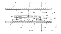
次に、電流検出装置6について図2〜5を参照して説明する。図2は、電流検出装置6の概略構成を示す斜視図である。また、各図においてXYZ座標系を示しており、XYZ座標系を用いて各方向を説明する。X方向(第2の方向)はバスバBの延在方向を示し、Y方向(第1の方向)はバスバBの平行配置の方向を示し、Z方向(第3の方向)は電流検出装置6の上下方向を示している。
Next, the
電流検出装置6は、U相、V相、W相のバスバBU,BV,BWを含むバスバBと、バスバBU,BV,BWの電流をそれぞれ検出する磁電変換素子SU,SV,SWと、磁電変換素子SU,SV,SWへの磁気干渉を抑制する一対の磁気シールド10,11とを備えている。
The
バスバBU,BV,BWは、Y方向において互いに平行に配置されており、X方向に延在している。磁気シールド10,11は、バスバBU,BV,BW及び磁電変換素子SU,SV,SWをZ方向において上下両側から挟み込むように配置されている。なお、バスバBU,BV,BW及び磁電変換素子SU,SV,SWの配置構成等を示すために、磁気シールド10を仮想線で示している。
The bus bars BU, BV, and BW are arranged parallel to each other in the Y direction and extend in the X direction. The
磁気シールド10,11は、例えば、高透磁率の鉄やフェライト等の磁性材料から形成されており、バスバBU,BV,BW及び磁電変換素子SU,SV,SWを覆うことが可能な平板形状である。また、磁気シールド11には、磁電変換素子SU,SV,SWが実装された基板PU,PV,PWがそれぞれ設けられている。
The
磁電変換素子SU,SV,SWは、バスバBU,BV,BWに電流が流れたときに発生する磁束を検出して、これに対応する電流値を算出するものである。磁電変換素子SU,SV,SWとしては、ホール素子、MI素子(磁気インピーダンス素子)、MR素子(磁気抵抗素子)等を使用することができる。 The magnetron conversion elements SU, SV, and SW detect the magnetic flux generated when a current flows through the bus bar BU, BV, and BW, and calculate the corresponding current value. As the magnetron conversion elements SU, SV, and SW, Hall elements, MI elements (magnetic impedance elements), MR elements (magneto resistance elements), and the like can be used.
次に、バスバBU,BV,BWの構成について詳しく説明する。バスバBU,BV,BWは、X方向に細長い平板形状の金属板により形成されている。バスバBU,BV,BWは、その幅広の側面が互いに対向するようにY方向に対して平行に配置されている。 Next, the configurations of the bus bars BU, BV, and BW will be described in detail. The bus bars BU, BV, and BW are formed of a flat metal plate elongated in the X direction. The bus bars BU, BV, and BW are arranged parallel to the Y direction so that their wide side surfaces face each other.
バスバBU,BV,BWは、幅広部BUL,BVL,BWLと、幅広部BUL,BVL,BWLを幅方向から切り欠いて形成された幅狭部BUS,BVS,BWSとを有している。幅狭部BUS,BVS,BWSの断面積は、幅広部BUL,BVL,BWLの断面積よりも小さい。また、幅広部BUL,BVL,BWLの断面積は互いに同一であり、幅狭部BUS,BVS,BWSの断面積も互いに同一である。 The bus bars BU, BV, and BW have wide portions BUL, BVL, and BWL, and narrow portions BUS, BVS, and BWS formed by cutting out the wide portions BUL, BVL, and BWL from the width direction. The cross-sectional area of the narrow portion BUS, BVS, BWS is smaller than the cross-sectional area of the wide portion BUL, BVL, BWL. Further, the cross-sectional areas of the wide portions BUL, BVL, and BWL are the same as each other, and the cross-sectional areas of the narrow portions BUS, BVS, and BWS are also the same.
幅広部BUL,BVL,BWLと幅狭部BUS,BVS,BWSとは、千鳥状に配置されている。すなわち、幅狭部BUSは隣接する幅狭部BVSと対向しないように、幅狭部BVSは隣接する幅狭部BWSと対向しないようにそれぞれ配置されている。換言すると、幅狭部BUS,BVS,BWSは、Z方向から見ると略V字状に配置されている。また、幅狭部BUS,BVS,BWSは、バスバBU,BV,BWに流れる電流を検出するための部分であり、幅狭部BUS,BVS,BWS以外は、幅広部BUL,BVL,BWLとなっている(図2のバスバBV参照)。 The wide portion BUL, BVL, BWL and the narrow portion BUS, BVS, BWS are arranged in a staggered pattern. That is, the narrow portion BUS is arranged so as not to face the adjacent narrow portion BVS, and the narrow portion BVS is arranged so as not to face the adjacent narrow portion BWS. In other words, the narrow portions BUS, BVS, and BWS are arranged in a substantially V shape when viewed from the Z direction. Further, the narrow portion BUS, BVS, BWS is a part for detecting the current flowing through the bus bur BU, BV, BW, and the narrow portion BUS, BVS, BWS is a wide portion BUL, BVL, BWL except for the narrow portion BUS, BVS, BWS. (See Busba BV in FIG. 2).
図4は、図3のb−b断面図を示している。図4において、符号WLCは、幅広部BWLの中心線を示している。また、符号WSCは、幅狭部BWSの中心線を示している。幅狭部BWSの中心線WSCは、幅広部BWLの中心線WLCに対して、距離DWだけ磁気シールド11側に近接している。すなわち、幅狭部BWSは、幅広部BWLに対して磁気シールド11側にオフセットして配置されている。この点について、図3を参照すると、幅狭部BWSは、磁気シールド10,11の間において、磁気シールド10との間隔が距離H1となり、磁気シールド11との間隔が距離H2(距離H1>距離H2)となって、磁気シールド11に近接して配置される。
FIG. 4 shows a cross-sectional view taken along the line bb of FIG. In FIG. 4, the reference numeral WLC indicates the center line of the wide portion BWL. Further, the reference numeral WSC indicates the center line of the narrow portion BWS. The center line WSC of the narrow portion BWS is closer to the
幅狭部BWSと磁気シールド11との間には、磁電変換素子SWが配置されている。磁電変換素子SWは、図3に示すように、幅狭部BWSに対向して感磁方向がY方向を向くように配置されている。
A magnetron conversion element SW is arranged between the narrow portion BWS and the
また、バスバBUはバスバBWと同様の構成であり、幅狭部BUSが幅広部BULに対して、磁気シールド11側にオフセットして配置されており、幅狭部BUSに対向する部分に磁電変換素子SUが配置されている。
Further, the bus bar BU has the same configuration as the bus bar BW, and the narrow portion BUS is arranged so as to be offset toward the
図2、5に示すように、バスバBVの幅狭部BVSはバスバBWの幅狭部BWSとは配置位置が異なっているが、バスバBWの幅狭部BWSと同様に、幅狭部BVSが幅広部BVLに対して磁気シールド11側にオフセットして配置されており、幅狭部BVSに対向する部分に磁電変換素子SVが配置されている。なお、図4、5においては、図面の煩雑化を避けるため他のバスバの図示を省略している。
As shown in FIGS. 2 and 5, the narrow portion BVS of the bus bar BV is arranged at a different position from the narrow portion BWS of the bus bar BW, but the narrow portion BVS is similar to the narrow portion BWS of the bus bar BW. The
次に、自相バスバの磁束を検出する際の他相バスバからの磁束の影響について説明する。ここでは、バスバBW(自相)の磁束を検出する際のバスバBV(他相)からの磁束の影響について説明するが、他のバスバBU、BVの関係についても同様である。 Next, the influence of the magnetic flux from the other-phase bus bar when detecting the magnetic flux of the self-phase bus bar will be described. Here, the influence of the magnetic flux from the bus bar BV (other phase) when detecting the magnetic flux of the bus bar BW (self-phase) will be described, but the same applies to the relationship between the other bus bar BU and BV.
図4、5において、バスバBV,BWを流れる電流の中心をそれぞれ電流IV,IWとして模式化して示す。図4に示すように、電流IWは、幅狭部BWSでは中心線WSCを通り、幅広部BWLでは中心線WLCを通る。このように、電流IWも、磁気シールド11側にオフセットされた状態で流れることになる。
In FIGS. 4 and 5, the centers of the currents flowing through the bus bars BV and BW are schematically shown as currents IV and IW, respectively. As shown in FIG. 4, the current IW passes through the center line WSC in the narrow portion BWS and passes through the center line WLC in the wide portion BWL. In this way, the current IW also flows in a state of being offset toward the
そして、幅狭部BWSを流れる電流IWを磁電変換素子SWによって検出する。幅狭部BWSは断面積が小さいので、電流IWが集中して流れる。このため、幅狭部BWSでは大きな磁束が発生する。磁電変換素子SWはこの磁束を検出して電流値に変換する。このとき、磁電変換素子SWは、図3において矢印で示すY方向成分の磁束を検出する。 Then, the current IW flowing through the narrow portion BWS is detected by the magnetron conversion element SW. Since the narrow cross-sectional area of the narrow portion BWS is small, the current IW flows in a concentrated manner. Therefore, a large magnetic flux is generated in the narrow portion BWS. The magnetron conversion element SW detects this magnetic flux and converts it into a current value. At this time, the magnetron conversion element SW detects the magnetic flux of the Y-direction component indicated by the arrow in FIG.
一方、図5に示すように、電流IVは、幅広部BVLでは中心線VLCを通り、幅狭部BVSでは中心線VSCを通る。つまり、電流IVは、中心線VLCから中心線VSCに沿うように流れる。このように、電流IVも、磁気シールド11側にオフセットされた状態で流れることになる。
On the other hand, as shown in FIG. 5, the current IV passes through the center line VLC in the wide portion BVL and passes through the center line VSC in the narrow portion BVS. That is, the current IV flows from the center line VLC along the center line VSC. In this way, the current IV also flows in a state of being offset toward the
図6に、磁電変換素子SWからみたときの電流IW,IVを重ねた状態を示す。図6に示すように、磁電変換素子SWに対して、電流IVが流れる位置は、電流IWが流れる位置よりも距離D1だけ離れているので、電流IVによる磁束の影響を受けにくくなる。この結果、電流IVの磁束の影響を抑制することができる。 FIG. 6 shows a state in which the currents IW and IV viewed from the magnetron conversion element SW are superimposed. As shown in FIG. 6, since the position where the current IV flows is separated from the position where the current IW flows by a distance D1 with respect to the magnetron conversion element SW, it is less likely to be affected by the magnetic flux due to the current IV. As a result, the influence of the magnetic flux of the current IV can be suppressed.
この理由について、図7、8を参照して説明する。図7は図2のa−a断面におけるY方向の磁束分布のシミュレーション結果を示し、図8は図3のb−b断面におけるY方向の磁束分布のシミュレーション結果を示している。図7、8において、符号GLは磁束が小さい領域を示し、符号GHは磁束が大きい領域を示している。 The reason for this will be described with reference to FIGS. 7 and 8. FIG. 7 shows the simulation result of the magnetic flux distribution in the Y direction in the cross section aa of FIG. 2, and FIG. 8 shows the simulation result of the magnetic flux distribution in the Y direction in the cross section bb of FIG. In FIGS. 7 and 8, the reference numeral GL indicates a region where the magnetic flux is small, and the reference numeral GH indicates a region where the magnetic flux is large.
図7において、バスバBVの上部の領域GH1の磁束が最も大きく、次にバスバBVの下部の領域GH2の磁束が大きい。また、磁気シールド10,11の近傍の領域では磁束が小さく、領域GH1,GH2から離れた領域GL1,GL2,GL3,GL4の磁束も小さい。特に、領域GL3,GL4の磁束が最も小さい。
In FIG. 7, the magnetic flux in the upper region GH1 of the bus bar BV is the largest, followed by the magnetic flux in the lower region GH2 of the bus bar BV. Further, the magnetic flux is small in the regions near the
図8において、バスバBWの幅狭部BWSの上方であって、磁気シールド10の後方の領域GH3の磁束が大きい。また、磁気シールド10,11の近傍の領域では磁束が小さく、領域GH3から離れた領域GL5,GL6,GL7の磁束も小さい。特に、領域GL6の磁束が最も小さい。なお、図7、8において、磁電変換素子SWを一点鎖線で示す。
In FIG. 8, the magnetic flux in the region GH3 above the narrow portion BWS of the bus bar BW and behind the
図6に示す磁電変換素子SWと電流IW,IVとの関係、図7、8に示すシミュレーション結果からわかるように、磁電変換素子SWの位置は、電流IVが流れる位置から離れており、電流IVによって発生する磁束の影響を受けにくくなっている。すなわち、磁電変換素子SWは、図7においては領域GL4に位置しており、図8においては領域GL6に位置している。このように、磁電変換素子SWは、バスバBVを流れる電流IVによる磁束の影響が小さい位置に配置されている。 As can be seen from the relationship between the magnetron conversion element SW shown in FIG. 6 and the currents IW and IV, and the simulation results shown in FIGS. 7 and 8, the position of the magnetron conversion element SW is far from the position where the current IV flows, and the current IV It is less susceptible to the magnetic flux generated by. That is, the magnetron conversion element SW is located in the region GL4 in FIG. 7, and is located in the region GL6 in FIG. As described above, the magnetron conversion element SW is arranged at a position where the influence of the magnetic flux due to the current IV flowing through the bus bar BV is small.
このため、上述したように、バスバBWの幅狭部BWSを磁気シールド11に近接するとともに、隣接するバスバBUの幅狭部BUSと互い違いに配置して、磁電変換素子SWを幅狭部BWSの近傍に配置することによって、バスバBWの磁束を良好に検出することができ、また、隣接するバスバBUの磁束の影響を抑制することができる。この結果、高精度な電流検出を行うことができる
Therefore, as described above, the narrow portion BWS of the bus bar BW is arranged close to the
また、一対の磁気シールド10,11によりバスバBをZ方向の両側から挟み込むように配置しているので、バスバBU,BV,BWを個別に囲む必要がなく、磁気シールドの部品点数を削減することができ、また、その大きさも小型化することができる。この結果、電流検出装置6を小型化することができ、部品点数の削減によりコストも低減することができる。よって、高精度な電流検出と、小型化及び低コスト化とを両立することができる。
Further, since the bus bar B is arranged so as to be sandwiched from both sides in the Z direction by the pair of
次に、第2の実施形態について図9、10を参照して説明する。第2の実施形態は、第1の実施形態とは磁気シールド12,13の構成が異なり、その他の構成については第1の実施形態と同様なので、磁気シールド12,13の構成について説明し、その他の構成についての説明は省略する。
Next, the second embodiment will be described with reference to FIGS. 9 and 10. In the second embodiment, the configurations of the
図10に示すように、磁気シールド12は、バスバBU,BV,BWの幅広部BUL,BVL,BWLに対応する部分がそれぞれ切り欠かれたスリット12U,12V,12Wを有している。磁気シールド13も同様に、スリット13U,13V,13Wを有している(図9参照)。
As shown in FIG. 10, the
このため、バスバBU,BV,BWの幅広部BUL,BVL,BWLを干渉することなく、磁気シールド12,13の間隔を狭めることができる。この結果、電流検出装置6のZ方向の大きさを小さくすることができる。第1の実施形態の電流検出装置6による効果に加え、電流検出装置6をさらに小型化することができる。
Therefore, the distance between the
次に、第3の実施形態について図11、12を参照して説明する。第3の実施形態は、第1の実施形態とはバスバBU,BV,BWの形状が異なり、その他の構成については第1の実施形態と同様なので、バスバBU,BV,BWの形状について説明し、その他の構成についての説明は省略する。 Next, the third embodiment will be described with reference to FIGS. 11 and 12. Since the shape of the bus bar BU, BV, and BW is different from that of the first embodiment and the other configurations are the same as those of the first embodiment, the shape of the bus bar BU, BV, and BW will be described. , Other configurations will be omitted.
図11、12に示すように、バスバBU,BV,BWの幅狭部BUS,BVS,BWSは、幅広部BUL,BVL,BWLの一側端側を切り欠くことによって形成されている。このため、バスバBU,BV,BWの幅狭部BUS,BVS,BWSを形成する際に、第1の実施形態のバスバBU,BV,BWと比べて、バスバBU,BV,BWの切り欠き加工工数を低減することができる。 As shown in FIGS. 11 and 12, the narrow portions BUS, BVS, and BWS of the bus bars BU, BV, and BW are formed by cutting out one side end side of the wide portions BUL, BVL, and BWL. Therefore, when forming the narrow portions BUS, BVS, and BWS of the bus bars BU, BV, and BW, the notch processing of the bus bars BU, BV, and BW is performed as compared with the bus bars BU, BV, and BW of the first embodiment. Man-hours can be reduced.
すなわち、第1の実施形態のバスバBU,BV,BWでは、幅広部BUL,BVL,BWLの両側から幅広部BUL,BVL,BWLを切り欠くことによって幅狭部BUS,BVS,BWSを形成していたが、第3の実施形態の幅狭部BUS,BVS,BWSは、幅広部BUL,BVL,BWLの片側のみを切り欠くことによって幅狭部BUS,BVS,BWSを形成することができるので、加工工数を低減することが可能になる。 That is, in the bus bus BU, BV, BW of the first embodiment, the narrow portion BUS, BVS, BWS is formed by cutting out the wide portion BUL, BVL, BWL from both sides of the wide portion BUL, BVL, BWL. However, since the narrow portion BUS, BVS, BWS of the third embodiment can form the narrow portion BUS, BVS, BWS by cutting out only one side of the wide portion BUL, BVL, BWL. It is possible to reduce the processing man-hours.
1 回転電機、2 直流電源、3 インバータ、4 モータジェネレータ、5 電力変換部、6 電流検出装置、7 制御装置、10,11,12,13 磁気シールド、B,BU,BV,BW バスバ、BUL,BVL,BWL 幅広部、BUS,BVS,BWS 幅狭部、GH1,GH2,GH3,GL1,GL2,GL3,GL4,GL5,GL6,GL7 領域、IV,IW 電流、PU,PV,PW 基板、SU,SV,SW 磁電変換素子、VLC,VSC,WLC,WSC 中心線。 1 rotary electric machine, 2 DC power supply, 3 inverter, 4 motor generator, 5 power converter, 6 current detector, 7 controller, 10, 11, 12, 13 magnetic shield, B, BU, BV, BW bus bar, BUL, BVL, BWL wide part, BUS, BVS, BWS narrow part, GH1, GH2, GH3, GL1, GL2, GL3, GL4, GL5, GL6, GL7 region, IV, IW current, PU, PV, PW substrate, SU, SV, SW magnetic conversion element, VLC, VSC, WLC, WSC center line.
Claims (2)
前記バスバに流れる電流を検出する磁電変換素子と、
前記第1の方向及び前記第2の方向に対して直交する第3の方向において、前記バスバ及び前記磁電変換素子を挟み込むように配置された一対の磁気シールドと、
を備えており、
前記各バスバは、側面から切り欠いた幅狭部を有し、前記幅狭部は、隣接する前記幅狭部と対向しない位置、かつ、一方の前記磁気シールドに近接する位置に配置され、
前記磁電変換素子は、前記幅狭部と前記幅狭部が近接する側の前記磁気シールドとの間に配置される、
ことを特徴とする電流検出装置。 A plurality of bus bars arranged parallel to the first direction and extending in a second direction orthogonal to the first direction, respectively.
A magnetron conversion element that detects the current flowing through the bus bar,
A pair of magnetic shields arranged so as to sandwich the bus bar and the magnetron conversion element in the first direction and the third direction orthogonal to the second direction.
Is equipped with
Each bus bar has a narrow portion cut out from the side surface, and the narrow portion is arranged at a position not facing the adjacent narrow portion and at a position close to one of the magnetic shields.
The magnetron conversion element is arranged between the narrow portion and the magnetic shield on the side where the narrow portion is close to each other.
A current detector characterized by this.
前記各バスバの前記幅狭部は、前記各バスバの一端側のみを切り欠くことにより形成されている、The narrow portion of each bus bar is formed by cutting out only one end side of each bus bar.
ことを特徴とする電流検出装置。A current detector characterized by this.
Priority Applications (1)
| Application Number | Priority Date | Filing Date | Title |
|---|---|---|---|
| JP2017064566A JP6878083B2 (en) | 2017-03-29 | 2017-03-29 | Current detector |
Applications Claiming Priority (1)
| Application Number | Priority Date | Filing Date | Title |
|---|---|---|---|
| JP2017064566A JP6878083B2 (en) | 2017-03-29 | 2017-03-29 | Current detector |
Publications (2)
| Publication Number | Publication Date |
|---|---|
| JP2018169188A JP2018169188A (en) | 2018-11-01 |
| JP6878083B2 true JP6878083B2 (en) | 2021-05-26 |
Family
ID=64019452
Family Applications (1)
| Application Number | Title | Priority Date | Filing Date |
|---|---|---|---|
| JP2017064566A Active JP6878083B2 (en) | 2017-03-29 | 2017-03-29 | Current detector |
Country Status (1)
| Country | Link |
|---|---|
| JP (1) | JP6878083B2 (en) |
Family Cites Families (8)
| Publication number | Priority date | Publication date | Assignee | Title |
|---|---|---|---|---|
| JP2010044025A (en) * | 2008-08-18 | 2010-02-25 | Tokai Rika Co Ltd | Current sensor |
| JP2011080970A (en) * | 2009-10-02 | 2011-04-21 | Kohshin Electric Corp | Detection device of multiphase current |
| CH703903B1 (en) * | 2010-10-01 | 2014-04-30 | Melexis Tessenderlo Nv | Current sensor. |
| JP2015194349A (en) * | 2014-03-31 | 2015-11-05 | 株式会社フジクラ | Current detection device |
| JP6237525B2 (en) * | 2014-08-05 | 2017-11-29 | トヨタ自動車株式会社 | Current sensor |
| JP2016125907A (en) * | 2015-01-05 | 2016-07-11 | トヨタ自動車株式会社 | Current sensor |
| JP2016161529A (en) * | 2015-03-05 | 2016-09-05 | トヨタ自動車株式会社 | Current sensor |
| JP2016200549A (en) * | 2015-04-14 | 2016-12-01 | トヨタ自動車株式会社 | Current-voltage sensor |
-
2017
- 2017-03-29 JP JP2017064566A patent/JP6878083B2/en active Active
Also Published As
| Publication number | Publication date |
|---|---|
| JP2018169188A (en) | 2018-11-01 |
Similar Documents
| Publication | Publication Date | Title |
|---|---|---|
| JP6362691B2 (en) | Current detector | |
| JP5153491B2 (en) | Current detector | |
| JP7047435B2 (en) | How to design a current sensor | |
| JP2016173334A (en) | Current sensor | |
| CN102713645B (en) | Current detection device | |
| JP5153481B2 (en) | Current detector | |
| JP6524877B2 (en) | Current sensor | |
| JP2019100923A (en) | Current sensor | |
| JP2018004314A (en) | Current sensor | |
| JPWO2016056135A1 (en) | Current detection device and current detection method | |
| JP2016173306A (en) | Busbar module | |
| CN112014615A (en) | Bus bar and power module with bus bar | |
| JP2018096794A (en) | Current sensor | |
| JP2016099111A (en) | Current sensor | |
| JP2008016770A (en) | Semiconductor module | |
| US10295571B2 (en) | Bus bar module | |
| JP6878083B2 (en) | Current detector | |
| JP6237525B2 (en) | Current sensor | |
| WO2022065311A1 (en) | Current detection device | |
| JP2016200549A (en) | Current-voltage sensor | |
| WO2020008844A1 (en) | Electric circuit device | |
| JP2021039030A (en) | Current sensor | |
| JP6869476B2 (en) | Current sensor | |
| WO2023136125A1 (en) | Electric current sensor device | |
| JP2023004468A (en) | current detector |
Legal Events
| Date | Code | Title | Description |
|---|---|---|---|
| A621 | Written request for application examination |
Free format text: JAPANESE INTERMEDIATE CODE: A621 Effective date: 20191108 |
|
| A977 | Report on retrieval |
Free format text: JAPANESE INTERMEDIATE CODE: A971007 Effective date: 20201023 |
|
| A131 | Notification of reasons for refusal |
Free format text: JAPANESE INTERMEDIATE CODE: A131 Effective date: 20201104 |
|
| A521 | Written amendment |
Free format text: JAPANESE INTERMEDIATE CODE: A523 Effective date: 20201222 |
|
| TRDD | Decision of grant or rejection written | ||
| A01 | Written decision to grant a patent or to grant a registration (utility model) |
Free format text: JAPANESE INTERMEDIATE CODE: A01 Effective date: 20210406 |
|
| A61 | First payment of annual fees (during grant procedure) |
Free format text: JAPANESE INTERMEDIATE CODE: A61 Effective date: 20210428 |
|
| R150 | Certificate of patent or registration of utility model |
Ref document number: 6878083 Country of ref document: JP Free format text: JAPANESE INTERMEDIATE CODE: R150 |