JP6873840B2 - Transistor - Google Patents
Transistor Download PDFInfo
- Publication number
- JP6873840B2 JP6873840B2 JP2017122406A JP2017122406A JP6873840B2 JP 6873840 B2 JP6873840 B2 JP 6873840B2 JP 2017122406 A JP2017122406 A JP 2017122406A JP 2017122406 A JP2017122406 A JP 2017122406A JP 6873840 B2 JP6873840 B2 JP 6873840B2
- Authority
- JP
- Japan
- Prior art keywords
- oxide
- insulator
- region
- conductor
- transistor
- Prior art date
- Legal status (The legal status is an assumption and is not a legal conclusion. Google has not performed a legal analysis and makes no representation as to the accuracy of the status listed.)
- Active
Links
- 239000012212 insulator Substances 0.000 claims description 554
- 229910044991 metal oxide Inorganic materials 0.000 claims description 137
- 150000004706 metal oxides Chemical class 0.000 claims description 131
- 229910052760 oxygen Inorganic materials 0.000 claims description 113
- 229910052721 tungsten Inorganic materials 0.000 claims description 34
- 229910052710 silicon Inorganic materials 0.000 claims description 31
- PXHVJJICTQNCMI-UHFFFAOYSA-N Nickel Chemical compound [Ni] PXHVJJICTQNCMI-UHFFFAOYSA-N 0.000 claims description 28
- XUIMIQQOPSSXEZ-UHFFFAOYSA-N Silicon Chemical group [Si] XUIMIQQOPSSXEZ-UHFFFAOYSA-N 0.000 claims description 28
- 229910052735 hafnium Inorganic materials 0.000 claims description 28
- 239000010703 silicon Chemical group 0.000 claims description 28
- 239000010937 tungsten Substances 0.000 claims description 27
- 229910052782 aluminium Inorganic materials 0.000 claims description 25
- 239000010936 titanium Substances 0.000 claims description 25
- WFKWXMTUELFFGS-UHFFFAOYSA-N tungsten Chemical compound [W] WFKWXMTUELFFGS-UHFFFAOYSA-N 0.000 claims description 25
- XEEYBQQBJWHFJM-UHFFFAOYSA-N Iron Chemical compound [Fe] XEEYBQQBJWHFJM-UHFFFAOYSA-N 0.000 claims description 24
- 229910052719 titanium Inorganic materials 0.000 claims description 23
- XAGFODPZIPBFFR-UHFFFAOYSA-N aluminium Chemical group [Al] XAGFODPZIPBFFR-UHFFFAOYSA-N 0.000 claims description 22
- 239000010949 copper Substances 0.000 claims description 22
- 229910052715 tantalum Inorganic materials 0.000 claims description 22
- 229910052733 gallium Inorganic materials 0.000 claims description 21
- 229910052725 zinc Inorganic materials 0.000 claims description 21
- RTAQQCXQSZGOHL-UHFFFAOYSA-N Titanium Chemical compound [Ti] RTAQQCXQSZGOHL-UHFFFAOYSA-N 0.000 claims description 20
- GUVRBAGPIYLISA-UHFFFAOYSA-N tantalum atom Chemical compound [Ta] GUVRBAGPIYLISA-UHFFFAOYSA-N 0.000 claims description 19
- 229910052802 copper Inorganic materials 0.000 claims description 18
- VBJZVLUMGGDVMO-UHFFFAOYSA-N hafnium atom Chemical compound [Hf] VBJZVLUMGGDVMO-UHFFFAOYSA-N 0.000 claims description 18
- RYGMFSIKBFXOCR-UHFFFAOYSA-N Copper Chemical compound [Cu] RYGMFSIKBFXOCR-UHFFFAOYSA-N 0.000 claims description 17
- GYHNNYVSQQEPJS-UHFFFAOYSA-N Gallium Chemical group [Ga] GYHNNYVSQQEPJS-UHFFFAOYSA-N 0.000 claims description 17
- ZOKXTWBITQBERF-UHFFFAOYSA-N Molybdenum Chemical compound [Mo] ZOKXTWBITQBERF-UHFFFAOYSA-N 0.000 claims description 17
- 229910052796 boron Inorganic materials 0.000 claims description 17
- 229910052749 magnesium Inorganic materials 0.000 claims description 17
- 239000011777 magnesium Substances 0.000 claims description 17
- 229910052750 molybdenum Inorganic materials 0.000 claims description 17
- 239000011733 molybdenum Substances 0.000 claims description 17
- 229910052726 zirconium Inorganic materials 0.000 claims description 17
- 229910052779 Neodymium Inorganic materials 0.000 claims description 16
- 229910052720 vanadium Inorganic materials 0.000 claims description 16
- 229910052732 germanium Inorganic materials 0.000 claims description 15
- ZOXJGFHDIHLPTG-UHFFFAOYSA-N Boron Chemical group [B] ZOXJGFHDIHLPTG-UHFFFAOYSA-N 0.000 claims description 14
- FYYHWMGAXLPEAU-UHFFFAOYSA-N Magnesium Chemical compound [Mg] FYYHWMGAXLPEAU-UHFFFAOYSA-N 0.000 claims description 14
- QCWXUUIWCKQGHC-UHFFFAOYSA-N Zirconium Chemical compound [Zr] QCWXUUIWCKQGHC-UHFFFAOYSA-N 0.000 claims description 14
- 229910052790 beryllium Inorganic materials 0.000 claims description 14
- GNPVGFCGXDBREM-UHFFFAOYSA-N germanium atom Chemical compound [Ge] GNPVGFCGXDBREM-UHFFFAOYSA-N 0.000 claims description 14
- 229910052759 nickel Inorganic materials 0.000 claims description 14
- 229910052684 Cerium Inorganic materials 0.000 claims description 13
- 229910052742 iron Inorganic materials 0.000 claims description 13
- QEFYFXOXNSNQGX-UHFFFAOYSA-N neodymium atom Chemical compound [Nd] QEFYFXOXNSNQGX-UHFFFAOYSA-N 0.000 claims description 13
- ATBAMAFKBVZNFJ-UHFFFAOYSA-N beryllium atom Chemical compound [Be] ATBAMAFKBVZNFJ-UHFFFAOYSA-N 0.000 claims description 11
- 229910052746 lanthanum Inorganic materials 0.000 claims description 10
- FZLIPJUXYLNCLC-UHFFFAOYSA-N lanthanum atom Chemical compound [La] FZLIPJUXYLNCLC-UHFFFAOYSA-N 0.000 claims description 10
- GWXLDORMOJMVQZ-UHFFFAOYSA-N cerium Chemical compound [Ce] GWXLDORMOJMVQZ-UHFFFAOYSA-N 0.000 claims 5
- LEONUFNNVUYDNQ-UHFFFAOYSA-N vanadium atom Chemical compound [V] LEONUFNNVUYDNQ-UHFFFAOYSA-N 0.000 claims 5
- 239000004020 conductor Substances 0.000 description 430
- 239000010408 film Substances 0.000 description 164
- 239000011701 zinc Substances 0.000 description 147
- 230000006870 function Effects 0.000 description 140
- 238000000034 method Methods 0.000 description 120
- 239000004065 semiconductor Substances 0.000 description 116
- 239000001301 oxygen Substances 0.000 description 102
- QVGXLLKOCUKJST-UHFFFAOYSA-N atomic oxygen Chemical compound [O] QVGXLLKOCUKJST-UHFFFAOYSA-N 0.000 description 100
- 239000000758 substrate Substances 0.000 description 84
- 239000010410 layer Substances 0.000 description 70
- 230000004888 barrier function Effects 0.000 description 65
- 229910052739 hydrogen Inorganic materials 0.000 description 65
- 239000001257 hydrogen Substances 0.000 description 64
- UFHFLCQGNIYNRP-UHFFFAOYSA-N Hydrogen Chemical compound [H][H] UFHFLCQGNIYNRP-UHFFFAOYSA-N 0.000 description 55
- 239000000463 material Substances 0.000 description 51
- IJGRMHOSHXDMSA-UHFFFAOYSA-N Atomic nitrogen Chemical compound N#N IJGRMHOSHXDMSA-UHFFFAOYSA-N 0.000 description 43
- 229910052814 silicon oxide Inorganic materials 0.000 description 41
- 239000013078 crystal Substances 0.000 description 33
- 238000003860 storage Methods 0.000 description 33
- 238000005229 chemical vapour deposition Methods 0.000 description 32
- 239000012535 impurity Substances 0.000 description 30
- VYPSYNLAJGMNEJ-UHFFFAOYSA-N Silicium dioxide Chemical compound O=[Si]=O VYPSYNLAJGMNEJ-UHFFFAOYSA-N 0.000 description 29
- 239000007789 gas Substances 0.000 description 29
- 238000010438 heat treatment Methods 0.000 description 28
- 230000015572 biosynthetic process Effects 0.000 description 26
- 238000004544 sputter deposition Methods 0.000 description 26
- 229910052581 Si3N4 Inorganic materials 0.000 description 25
- 238000000231 atomic layer deposition Methods 0.000 description 25
- -1 berylium Chemical compound 0.000 description 25
- HQVNEWCFYHHQES-UHFFFAOYSA-N silicon nitride Chemical compound N12[Si]34N5[Si]62N3[Si]51N64 HQVNEWCFYHHQES-UHFFFAOYSA-N 0.000 description 23
- 229910052738 indium Inorganic materials 0.000 description 22
- TWNQGVIAIRXVLR-UHFFFAOYSA-N oxo(oxoalumanyloxy)alumane Chemical compound O=[Al]O[Al]=O TWNQGVIAIRXVLR-UHFFFAOYSA-N 0.000 description 21
- XLYOFNOQVPJJNP-UHFFFAOYSA-N water Substances O XLYOFNOQVPJJNP-UHFFFAOYSA-N 0.000 description 21
- 229910001868 water Inorganic materials 0.000 description 21
- 229910052751 metal Inorganic materials 0.000 description 19
- XKRFYHLGVUSROY-UHFFFAOYSA-N Argon Chemical compound [Ar] XKRFYHLGVUSROY-UHFFFAOYSA-N 0.000 description 18
- 239000002184 metal Substances 0.000 description 18
- 238000004549 pulsed laser deposition Methods 0.000 description 18
- APFVFJFRJDLVQX-UHFFFAOYSA-N indium atom Chemical compound [In] APFVFJFRJDLVQX-UHFFFAOYSA-N 0.000 description 17
- 229910052757 nitrogen Inorganic materials 0.000 description 17
- XLOMVQKBTHCTTD-UHFFFAOYSA-N Zinc monoxide Chemical compound [Zn]=O XLOMVQKBTHCTTD-UHFFFAOYSA-N 0.000 description 16
- 238000001451 molecular beam epitaxy Methods 0.000 description 15
- 206010021143 Hypoxia Diseases 0.000 description 13
- 125000004429 atom Chemical group 0.000 description 13
- 238000005530 etching Methods 0.000 description 13
- 230000001965 increasing effect Effects 0.000 description 13
- 239000000203 mixture Substances 0.000 description 13
- 238000004519 manufacturing process Methods 0.000 description 12
- 230000003647 oxidation Effects 0.000 description 12
- 238000007254 oxidation reaction Methods 0.000 description 12
- 239000012298 atmosphere Substances 0.000 description 11
- 238000009792 diffusion process Methods 0.000 description 11
- 238000001312 dry etching Methods 0.000 description 11
- 230000008569 process Effects 0.000 description 11
- 230000005684 electric field Effects 0.000 description 10
- 229910000449 hafnium oxide Inorganic materials 0.000 description 10
- WIHZLLGSGQNAGK-UHFFFAOYSA-N hafnium(4+);oxygen(2-) Chemical compound [O-2].[O-2].[Hf+4] WIHZLLGSGQNAGK-UHFFFAOYSA-N 0.000 description 10
- AMGQUBHHOARCQH-UHFFFAOYSA-N indium;oxotin Chemical compound [In].[Sn]=O AMGQUBHHOARCQH-UHFFFAOYSA-N 0.000 description 10
- 229910052786 argon Inorganic materials 0.000 description 9
- 150000002431 hydrogen Chemical class 0.000 description 9
- MZLGASXMSKOWSE-UHFFFAOYSA-N tantalum nitride Chemical compound [Ta]#N MZLGASXMSKOWSE-UHFFFAOYSA-N 0.000 description 9
- KRHYYFGTRYWZRS-UHFFFAOYSA-N Fluorane Chemical compound F KRHYYFGTRYWZRS-UHFFFAOYSA-N 0.000 description 8
- AJNVQOSZGJRYEI-UHFFFAOYSA-N digallium;oxygen(2-) Chemical compound [O-2].[O-2].[O-2].[Ga+3].[Ga+3] AJNVQOSZGJRYEI-UHFFFAOYSA-N 0.000 description 8
- 229910001195 gallium oxide Inorganic materials 0.000 description 8
- 150000004767 nitrides Chemical class 0.000 description 8
- 230000002093 peripheral effect Effects 0.000 description 8
- 239000011347 resin Substances 0.000 description 8
- 229920005989 resin Polymers 0.000 description 8
- 229910052718 tin Inorganic materials 0.000 description 8
- 239000011787 zinc oxide Substances 0.000 description 8
- OKTJSMMVPCPJKN-UHFFFAOYSA-N Carbon Chemical compound [C] OKTJSMMVPCPJKN-UHFFFAOYSA-N 0.000 description 7
- MYMOFIZGZYHOMD-UHFFFAOYSA-N Dioxygen Chemical compound O=O MYMOFIZGZYHOMD-UHFFFAOYSA-N 0.000 description 7
- 239000000956 alloy Substances 0.000 description 7
- 239000002131 composite material Substances 0.000 description 7
- 238000010586 diagram Methods 0.000 description 7
- 229910001882 dioxygen Inorganic materials 0.000 description 7
- 238000002149 energy-dispersive X-ray emission spectroscopy Methods 0.000 description 7
- 230000005669 field effect Effects 0.000 description 7
- 230000003071 parasitic effect Effects 0.000 description 7
- GPPXJZIENCGNKB-UHFFFAOYSA-N vanadium Chemical compound [V]#[V] GPPXJZIENCGNKB-UHFFFAOYSA-N 0.000 description 7
- 229910052727 yttrium Inorganic materials 0.000 description 7
- GWEVSGVZZGPLCZ-UHFFFAOYSA-N Titan oxide Chemical compound O=[Ti]=O GWEVSGVZZGPLCZ-UHFFFAOYSA-N 0.000 description 6
- NRTOMJZYCJJWKI-UHFFFAOYSA-N Titanium nitride Chemical compound [Ti]#N NRTOMJZYCJJWKI-UHFFFAOYSA-N 0.000 description 6
- HCHKCACWOHOZIP-UHFFFAOYSA-N Zinc Chemical compound [Zn] HCHKCACWOHOZIP-UHFFFAOYSA-N 0.000 description 6
- 229910052799 carbon Inorganic materials 0.000 description 6
- 230000007547 defect Effects 0.000 description 6
- 229910003437 indium oxide Inorganic materials 0.000 description 6
- PJXISJQVUVHSOJ-UHFFFAOYSA-N indium(iii) oxide Chemical compound [O-2].[O-2].[O-2].[In+3].[In+3] PJXISJQVUVHSOJ-UHFFFAOYSA-N 0.000 description 6
- 239000012528 membrane Substances 0.000 description 6
- QGLKJKCYBOYXKC-UHFFFAOYSA-N nonaoxidotritungsten Chemical compound O=[W]1(=O)O[W](=O)(=O)O[W](=O)(=O)O1 QGLKJKCYBOYXKC-UHFFFAOYSA-N 0.000 description 6
- 238000009832 plasma treatment Methods 0.000 description 6
- 238000002230 thermal chemical vapour deposition Methods 0.000 description 6
- 239000010409 thin film Substances 0.000 description 6
- OGIDPMRJRNCKJF-UHFFFAOYSA-N titanium oxide Inorganic materials [Ti]=O OGIDPMRJRNCKJF-UHFFFAOYSA-N 0.000 description 6
- 229910001930 tungsten oxide Inorganic materials 0.000 description 6
- YVTHLONGBIQYBO-UHFFFAOYSA-N zinc indium(3+) oxygen(2-) Chemical compound [O--].[Zn++].[In+3] YVTHLONGBIQYBO-UHFFFAOYSA-N 0.000 description 6
- PXGOKWXKJXAPGV-UHFFFAOYSA-N Fluorine Chemical compound FF PXGOKWXKJXAPGV-UHFFFAOYSA-N 0.000 description 5
- OAICVXFJPJFONN-UHFFFAOYSA-N Phosphorus Chemical compound [P] OAICVXFJPJFONN-UHFFFAOYSA-N 0.000 description 5
- 229910045601 alloy Inorganic materials 0.000 description 5
- ZMIGMASIKSOYAM-UHFFFAOYSA-N cerium Chemical compound [Ce][Ce][Ce][Ce][Ce][Ce][Ce][Ce][Ce][Ce][Ce][Ce][Ce][Ce][Ce][Ce][Ce][Ce][Ce][Ce][Ce][Ce][Ce][Ce][Ce][Ce][Ce][Ce][Ce][Ce][Ce][Ce][Ce][Ce][Ce][Ce][Ce][Ce] ZMIGMASIKSOYAM-UHFFFAOYSA-N 0.000 description 5
- 238000006243 chemical reaction Methods 0.000 description 5
- 239000011651 chromium Substances 0.000 description 5
- PMHQVHHXPFUNSP-UHFFFAOYSA-M copper(1+);methylsulfanylmethane;bromide Chemical compound Br[Cu].CSC PMHQVHHXPFUNSP-UHFFFAOYSA-M 0.000 description 5
- 230000006378 damage Effects 0.000 description 5
- 229910001873 dinitrogen Inorganic materials 0.000 description 5
- 230000000694 effects Effects 0.000 description 5
- 229910052731 fluorine Inorganic materials 0.000 description 5
- 239000011737 fluorine Substances 0.000 description 5
- 238000001459 lithography Methods 0.000 description 5
- 238000013507 mapping Methods 0.000 description 5
- 239000007769 metal material Substances 0.000 description 5
- 229910052698 phosphorus Inorganic materials 0.000 description 5
- 239000011574 phosphorus Substances 0.000 description 5
- 239000002994 raw material Substances 0.000 description 5
- JBRZTFJDHDCESZ-UHFFFAOYSA-N AsGa Chemical compound [As]#[Ga] JBRZTFJDHDCESZ-UHFFFAOYSA-N 0.000 description 4
- VYZAMTAEIAYCRO-UHFFFAOYSA-N Chromium Chemical compound [Cr] VYZAMTAEIAYCRO-UHFFFAOYSA-N 0.000 description 4
- 229910001218 Gallium arsenide Inorganic materials 0.000 description 4
- 229910052804 chromium Inorganic materials 0.000 description 4
- 150000001875 compounds Chemical class 0.000 description 4
- 230000007423 decrease Effects 0.000 description 4
- 239000010931 gold Substances 0.000 description 4
- 239000011261 inert gas Substances 0.000 description 4
- 238000009413 insulation Methods 0.000 description 4
- 230000010354 integration Effects 0.000 description 4
- MRELNEQAGSRDBK-UHFFFAOYSA-N lanthanum(3+);oxygen(2-) Chemical compound [O-2].[O-2].[O-2].[La+3].[La+3] MRELNEQAGSRDBK-UHFFFAOYSA-N 0.000 description 4
- 239000002105 nanoparticle Substances 0.000 description 4
- PLDDOISOJJCEMH-UHFFFAOYSA-N neodymium(3+);oxygen(2-) Chemical compound [O-2].[O-2].[O-2].[Nd+3].[Nd+3] PLDDOISOJJCEMH-UHFFFAOYSA-N 0.000 description 4
- 239000012299 nitrogen atmosphere Substances 0.000 description 4
- 238000005268 plasma chemical vapour deposition Methods 0.000 description 4
- BASFCYQUMIYNBI-UHFFFAOYSA-N platinum Chemical compound [Pt] BASFCYQUMIYNBI-UHFFFAOYSA-N 0.000 description 4
- 239000000243 solution Substances 0.000 description 4
- 238000001039 wet etching Methods 0.000 description 4
- VWQVUPCCIRVNHF-UHFFFAOYSA-N yttrium atom Chemical group [Y] VWQVUPCCIRVNHF-UHFFFAOYSA-N 0.000 description 4
- ZAMOUSCENKQFHK-UHFFFAOYSA-N Chlorine atom Chemical compound [Cl] ZAMOUSCENKQFHK-UHFFFAOYSA-N 0.000 description 3
- 229910000577 Silicon-germanium Inorganic materials 0.000 description 3
- BQCADISMDOOEFD-UHFFFAOYSA-N Silver Chemical compound [Ag] BQCADISMDOOEFD-UHFFFAOYSA-N 0.000 description 3
- ATJFFYVFTNAWJD-UHFFFAOYSA-N Tin Chemical compound [Sn] ATJFFYVFTNAWJD-UHFFFAOYSA-N 0.000 description 3
- 238000002441 X-ray diffraction Methods 0.000 description 3
- 230000009471 action Effects 0.000 description 3
- 230000003321 amplification Effects 0.000 description 3
- 238000004458 analytical method Methods 0.000 description 3
- 239000004760 aramid Substances 0.000 description 3
- 229920003235 aromatic polyamide Polymers 0.000 description 3
- 239000000969 carrier Substances 0.000 description 3
- 230000008859 change Effects 0.000 description 3
- 229910052801 chlorine Inorganic materials 0.000 description 3
- 239000000460 chlorine Substances 0.000 description 3
- 238000007667 floating Methods 0.000 description 3
- 239000011521 glass Substances 0.000 description 3
- PCHJSUWPFVWCPO-UHFFFAOYSA-N gold Chemical compound [Au] PCHJSUWPFVWCPO-UHFFFAOYSA-N 0.000 description 3
- 229910052737 gold Inorganic materials 0.000 description 3
- 239000013081 microcrystal Substances 0.000 description 3
- 238000003199 nucleic acid amplification method Methods 0.000 description 3
- 238000012545 processing Methods 0.000 description 3
- 229910052709 silver Inorganic materials 0.000 description 3
- 239000004332 silver Substances 0.000 description 3
- 239000002356 single layer Substances 0.000 description 3
- 239000000126 substance Substances 0.000 description 3
- 239000004677 Nylon Substances 0.000 description 2
- 239000004952 Polyamide Substances 0.000 description 2
- 239000004642 Polyimide Substances 0.000 description 2
- 229910020994 Sn-Zn Inorganic materials 0.000 description 2
- 229910008813 Sn—Si Inorganic materials 0.000 description 2
- 229910009069 Sn—Zn Inorganic materials 0.000 description 2
- 229910007541 Zn O Inorganic materials 0.000 description 2
- LEVVHYCKPQWKOP-UHFFFAOYSA-N [Si].[Ge] Chemical compound [Si].[Ge] LEVVHYCKPQWKOP-UHFFFAOYSA-N 0.000 description 2
- NIXOWILDQLNWCW-UHFFFAOYSA-N acrylic acid group Chemical group C(C=C)(=O)O NIXOWILDQLNWCW-UHFFFAOYSA-N 0.000 description 2
- 238000005054 agglomeration Methods 0.000 description 2
- 230000002776 aggregation Effects 0.000 description 2
- 229910052785 arsenic Inorganic materials 0.000 description 2
- RQNWIZPPADIBDY-UHFFFAOYSA-N arsenic atom Chemical compound [As] RQNWIZPPADIBDY-UHFFFAOYSA-N 0.000 description 2
- 238000005452 bending Methods 0.000 description 2
- 230000005540 biological transmission Effects 0.000 description 2
- 238000013461 design Methods 0.000 description 2
- 230000006866 deterioration Effects 0.000 description 2
- 238000010894 electron beam technology Methods 0.000 description 2
- 239000000835 fiber Substances 0.000 description 2
- YBMRDBCBODYGJE-UHFFFAOYSA-N germanium oxide Inorganic materials O=[Ge]=O YBMRDBCBODYGJE-UHFFFAOYSA-N 0.000 description 2
- 230000001939 inductive effect Effects 0.000 description 2
- 238000010884 ion-beam technique Methods 0.000 description 2
- 239000004973 liquid crystal related substance Substances 0.000 description 2
- CPLXHLVBOLITMK-UHFFFAOYSA-N magnesium oxide Inorganic materials [Mg]=O CPLXHLVBOLITMK-UHFFFAOYSA-N 0.000 description 2
- 239000000395 magnesium oxide Substances 0.000 description 2
- AXZKOIWUVFPNLO-UHFFFAOYSA-N magnesium;oxygen(2-) Chemical compound [O-2].[Mg+2] AXZKOIWUVFPNLO-UHFFFAOYSA-N 0.000 description 2
- 239000011572 manganese Substances 0.000 description 2
- WPBNNNQJVZRUHP-UHFFFAOYSA-L manganese(2+);methyl n-[[2-(methoxycarbonylcarbamothioylamino)phenyl]carbamothioyl]carbamate;n-[2-(sulfidocarbothioylamino)ethyl]carbamodithioate Chemical compound [Mn+2].[S-]C(=S)NCCNC([S-])=S.COC(=O)NC(=S)NC1=CC=CC=C1NC(=S)NC(=O)OC WPBNNNQJVZRUHP-UHFFFAOYSA-L 0.000 description 2
- 239000011159 matrix material Substances 0.000 description 2
- 238000012986 modification Methods 0.000 description 2
- 230000004048 modification Effects 0.000 description 2
- 229910052758 niobium Inorganic materials 0.000 description 2
- 239000010955 niobium Substances 0.000 description 2
- GUCVJGMIXFAOAE-UHFFFAOYSA-N niobium atom Chemical compound [Nb] GUCVJGMIXFAOAE-UHFFFAOYSA-N 0.000 description 2
- MWUXSHHQAYIFBG-UHFFFAOYSA-N nitrogen oxide Inorganic materials O=[N] MWUXSHHQAYIFBG-UHFFFAOYSA-N 0.000 description 2
- 229920001778 nylon Polymers 0.000 description 2
- 230000001590 oxidative effect Effects 0.000 description 2
- SIWVEOZUMHYXCS-UHFFFAOYSA-N oxo(oxoyttriooxy)yttrium Chemical compound O=[Y]O[Y]=O SIWVEOZUMHYXCS-UHFFFAOYSA-N 0.000 description 2
- PVADDRMAFCOOPC-UHFFFAOYSA-N oxogermanium Chemical compound [Ge]=O PVADDRMAFCOOPC-UHFFFAOYSA-N 0.000 description 2
- BPUBBGLMJRNUCC-UHFFFAOYSA-N oxygen(2-);tantalum(5+) Chemical compound [O-2].[O-2].[O-2].[O-2].[O-2].[Ta+5].[Ta+5] BPUBBGLMJRNUCC-UHFFFAOYSA-N 0.000 description 2
- RVTZCBVAJQQJTK-UHFFFAOYSA-N oxygen(2-);zirconium(4+) Chemical compound [O-2].[O-2].[Zr+4] RVTZCBVAJQQJTK-UHFFFAOYSA-N 0.000 description 2
- 239000002245 particle Substances 0.000 description 2
- 238000000623 plasma-assisted chemical vapour deposition Methods 0.000 description 2
- 229910052697 platinum Inorganic materials 0.000 description 2
- 229920002647 polyamide Polymers 0.000 description 2
- 229920000515 polycarbonate Polymers 0.000 description 2
- 239000004417 polycarbonate Substances 0.000 description 2
- 229910021420 polycrystalline silicon Inorganic materials 0.000 description 2
- 229920000728 polyester Polymers 0.000 description 2
- 229920001721 polyimide Polymers 0.000 description 2
- 229920000098 polyolefin Polymers 0.000 description 2
- 239000011148 porous material Substances 0.000 description 2
- 239000000047 product Substances 0.000 description 2
- 230000001681 protective effect Effects 0.000 description 2
- 239000011819 refractory material Substances 0.000 description 2
- 230000000717 retained effect Effects 0.000 description 2
- 239000013589 supplement Substances 0.000 description 2
- 229910001936 tantalum oxide Inorganic materials 0.000 description 2
- 238000012360 testing method Methods 0.000 description 2
- 238000004402 ultra-violet photoelectron spectroscopy Methods 0.000 description 2
- 229910001928 zirconium oxide Inorganic materials 0.000 description 2
- 229910018137 Al-Zn Inorganic materials 0.000 description 1
- 229910018573 Al—Zn Inorganic materials 0.000 description 1
- FIPWRIJSWJWJAI-UHFFFAOYSA-N Butyl carbitol 6-propylpiperonyl ether Chemical compound C1=C(CCC)C(COCCOCCOCCCC)=CC2=C1OCO2 FIPWRIJSWJWJAI-UHFFFAOYSA-N 0.000 description 1
- 229910017518 Cu Zn Inorganic materials 0.000 description 1
- 229910017752 Cu-Zn Inorganic materials 0.000 description 1
- 229910017943 Cu—Zn Inorganic materials 0.000 description 1
- 238000004435 EPR spectroscopy Methods 0.000 description 1
- GPXJNWSHGFTCBW-UHFFFAOYSA-N Indium phosphide Chemical compound [In]#P GPXJNWSHGFTCBW-UHFFFAOYSA-N 0.000 description 1
- PWHULOQIROXLJO-UHFFFAOYSA-N Manganese Chemical compound [Mn] PWHULOQIROXLJO-UHFFFAOYSA-N 0.000 description 1
- 229910018605 Ni—Zn Inorganic materials 0.000 description 1
- 229910006776 Si—Zn Inorganic materials 0.000 description 1
- 229910010967 Ti—Sn Inorganic materials 0.000 description 1
- 229910001080 W alloy Inorganic materials 0.000 description 1
- 238000010521 absorption reaction Methods 0.000 description 1
- MDPILPRLPQYEEN-UHFFFAOYSA-N aluminium arsenide Chemical compound [As]#[Al] MDPILPRLPQYEEN-UHFFFAOYSA-N 0.000 description 1
- 239000007864 aqueous solution Substances 0.000 description 1
- 238000004380 ashing Methods 0.000 description 1
- GPBUGPUPKAGMDK-UHFFFAOYSA-N azanylidynemolybdenum Chemical compound [Mo]#N GPBUGPUPKAGMDK-UHFFFAOYSA-N 0.000 description 1
- 230000000903 blocking effect Effects 0.000 description 1
- 229910052810 boron oxide Inorganic materials 0.000 description 1
- 230000015556 catabolic process Effects 0.000 description 1
- 238000004140 cleaning Methods 0.000 description 1
- 229910017052 cobalt Inorganic materials 0.000 description 1
- 239000010941 cobalt Substances 0.000 description 1
- GUTLYIVDDKVIGB-UHFFFAOYSA-N cobalt atom Chemical compound [Co] GUTLYIVDDKVIGB-UHFFFAOYSA-N 0.000 description 1
- 230000000295 complement effect Effects 0.000 description 1
- 239000000470 constituent Substances 0.000 description 1
- 238000012937 correction Methods 0.000 description 1
- 229910021419 crystalline silicon Inorganic materials 0.000 description 1
- 230000002950 deficient Effects 0.000 description 1
- JKWMSGQKBLHBQQ-UHFFFAOYSA-N diboron trioxide Chemical compound O=BOB=O JKWMSGQKBLHBQQ-UHFFFAOYSA-N 0.000 description 1
- 239000003989 dielectric material Substances 0.000 description 1
- 238000007865 diluting Methods 0.000 description 1
- 230000005685 electric field effect Effects 0.000 description 1
- 238000002003 electron diffraction Methods 0.000 description 1
- 238000002524 electron diffraction data Methods 0.000 description 1
- 238000000605 extraction Methods 0.000 description 1
- 239000011888 foil Substances 0.000 description 1
- 230000007274 generation of a signal involved in cell-cell signaling Effects 0.000 description 1
- 229910002804 graphite Inorganic materials 0.000 description 1
- 239000010439 graphite Substances 0.000 description 1
- 239000001307 helium Substances 0.000 description 1
- 229910052734 helium Inorganic materials 0.000 description 1
- SWQJXJOGLNCZEY-UHFFFAOYSA-N helium atom Chemical compound [He] SWQJXJOGLNCZEY-UHFFFAOYSA-N 0.000 description 1
- 238000007654 immersion Methods 0.000 description 1
- NJWNEWQMQCGRDO-UHFFFAOYSA-N indium zinc Chemical compound [Zn].[In] NJWNEWQMQCGRDO-UHFFFAOYSA-N 0.000 description 1
- 238000009616 inductively coupled plasma Methods 0.000 description 1
- 230000008595 infiltration Effects 0.000 description 1
- 238000001764 infiltration Methods 0.000 description 1
- 239000011229 interlayer Substances 0.000 description 1
- 238000005468 ion implantation Methods 0.000 description 1
- 229910052743 krypton Inorganic materials 0.000 description 1
- DNNSSWSSYDEUBZ-UHFFFAOYSA-N krypton atom Chemical compound [Kr] DNNSSWSSYDEUBZ-UHFFFAOYSA-N 0.000 description 1
- 238000010030 laminating Methods 0.000 description 1
- 239000007788 liquid Substances 0.000 description 1
- 229910052748 manganese Inorganic materials 0.000 description 1
- 238000005259 measurement Methods 0.000 description 1
- 239000011156 metal matrix composite Substances 0.000 description 1
- 238000002488 metal-organic chemical vapour deposition Methods 0.000 description 1
- 238000002156 mixing Methods 0.000 description 1
- MGRWKWACZDFZJT-UHFFFAOYSA-N molybdenum tungsten Chemical compound [Mo].[W] MGRWKWACZDFZJT-UHFFFAOYSA-N 0.000 description 1
- 239000002159 nanocrystal Substances 0.000 description 1
- 229910000480 nickel oxide Inorganic materials 0.000 description 1
- RUFLMLWJRZAWLJ-UHFFFAOYSA-N nickel silicide Chemical compound [Ni]=[Si]=[Ni] RUFLMLWJRZAWLJ-UHFFFAOYSA-N 0.000 description 1
- 229910021334 nickel silicide Inorganic materials 0.000 description 1
- 238000007645 offset printing Methods 0.000 description 1
- 230000003287 optical effect Effects 0.000 description 1
- 125000002524 organometallic group Chemical group 0.000 description 1
- 230000001151 other effect Effects 0.000 description 1
- GNRSAWUEBMWBQH-UHFFFAOYSA-N oxonickel Chemical compound [Ni]=O GNRSAWUEBMWBQH-UHFFFAOYSA-N 0.000 description 1
- 239000012466 permeate Substances 0.000 description 1
- 230000000704 physical effect Effects 0.000 description 1
- 238000001020 plasma etching Methods 0.000 description 1
- 238000005498 polishing Methods 0.000 description 1
- 238000010248 power generation Methods 0.000 description 1
- 238000007639 printing Methods 0.000 description 1
- 239000010453 quartz Substances 0.000 description 1
- 229910052594 sapphire Inorganic materials 0.000 description 1
- 239000010980 sapphire Substances 0.000 description 1
- 229910052706 scandium Inorganic materials 0.000 description 1
- SIXSYDAISGFNSX-UHFFFAOYSA-N scandium atom Chemical compound [Sc] SIXSYDAISGFNSX-UHFFFAOYSA-N 0.000 description 1
- 238000007650 screen-printing Methods 0.000 description 1
- 229910021332 silicide Inorganic materials 0.000 description 1
- FVBUAEGBCNSCDD-UHFFFAOYSA-N silicide(4-) Chemical compound [Si-4] FVBUAEGBCNSCDD-UHFFFAOYSA-N 0.000 description 1
- HBMJWWWQQXIZIP-UHFFFAOYSA-N silicon carbide Chemical compound [Si+]#[C-] HBMJWWWQQXIZIP-UHFFFAOYSA-N 0.000 description 1
- 229910010271 silicon carbide Inorganic materials 0.000 description 1
- 238000001179 sorption measurement Methods 0.000 description 1
- 238000004528 spin coating Methods 0.000 description 1
- 229910002076 stabilized zirconia Inorganic materials 0.000 description 1
- JBQYATWDVHIOAR-UHFFFAOYSA-N tellanylidenegermanium Chemical compound [Te]=[Ge] JBQYATWDVHIOAR-UHFFFAOYSA-N 0.000 description 1
- 230000008719 thickening Effects 0.000 description 1
- 238000012546 transfer Methods 0.000 description 1
- 229910052724 xenon Inorganic materials 0.000 description 1
- FHNFHKCVQCLJFQ-UHFFFAOYSA-N xenon atom Chemical compound [Xe] FHNFHKCVQCLJFQ-UHFFFAOYSA-N 0.000 description 1
- 229910001233 yttria-stabilized zirconia Inorganic materials 0.000 description 1
Images


Classifications
-
- H—ELECTRICITY
- H01—ELECTRIC ELEMENTS
- H01L—SEMICONDUCTOR DEVICES NOT COVERED BY CLASS H10
- H01L29/00—Semiconductor devices adapted for rectifying, amplifying, oscillating or switching, or capacitors or resistors with at least one potential-jump barrier or surface barrier, e.g. PN junction depletion layer or carrier concentration layer; Details of semiconductor bodies or of electrodes thereof ; Multistep manufacturing processes therefor
- H01L29/66—Types of semiconductor device ; Multistep manufacturing processes therefor
- H01L29/68—Types of semiconductor device ; Multistep manufacturing processes therefor controllable by only the electric current supplied, or only the electric potential applied, to an electrode which does not carry the current to be rectified, amplified or switched
- H01L29/76—Unipolar devices, e.g. field effect transistors
- H01L29/772—Field effect transistors
- H01L29/78—Field effect transistors with field effect produced by an insulated gate
- H01L29/786—Thin film transistors, i.e. transistors with a channel being at least partly a thin film
- H01L29/7869—Thin film transistors, i.e. transistors with a channel being at least partly a thin film having a semiconductor body comprising an oxide semiconductor material, e.g. zinc oxide, copper aluminium oxide, cadmium stannate
-
- H—ELECTRICITY
- H01—ELECTRIC ELEMENTS
- H01L—SEMICONDUCTOR DEVICES NOT COVERED BY CLASS H10
- H01L27/00—Devices consisting of a plurality of semiconductor or other solid-state components formed in or on a common substrate
- H01L27/02—Devices consisting of a plurality of semiconductor or other solid-state components formed in or on a common substrate including semiconductor components specially adapted for rectifying, oscillating, amplifying or switching and having at least one potential-jump barrier or surface barrier; including integrated passive circuit elements with at least one potential-jump barrier or surface barrier
- H01L27/12—Devices consisting of a plurality of semiconductor or other solid-state components formed in or on a common substrate including semiconductor components specially adapted for rectifying, oscillating, amplifying or switching and having at least one potential-jump barrier or surface barrier; including integrated passive circuit elements with at least one potential-jump barrier or surface barrier the substrate being other than a semiconductor body, e.g. an insulating body
- H01L27/1214—Devices consisting of a plurality of semiconductor or other solid-state components formed in or on a common substrate including semiconductor components specially adapted for rectifying, oscillating, amplifying or switching and having at least one potential-jump barrier or surface barrier; including integrated passive circuit elements with at least one potential-jump barrier or surface barrier the substrate being other than a semiconductor body, e.g. an insulating body comprising a plurality of TFTs formed on a non-semiconducting substrate, e.g. driving circuits for AMLCDs
- H01L27/1222—Devices consisting of a plurality of semiconductor or other solid-state components formed in or on a common substrate including semiconductor components specially adapted for rectifying, oscillating, amplifying or switching and having at least one potential-jump barrier or surface barrier; including integrated passive circuit elements with at least one potential-jump barrier or surface barrier the substrate being other than a semiconductor body, e.g. an insulating body comprising a plurality of TFTs formed on a non-semiconducting substrate, e.g. driving circuits for AMLCDs with a particular composition, shape or crystalline structure of the active layer
- H01L27/1225—Devices consisting of a plurality of semiconductor or other solid-state components formed in or on a common substrate including semiconductor components specially adapted for rectifying, oscillating, amplifying or switching and having at least one potential-jump barrier or surface barrier; including integrated passive circuit elements with at least one potential-jump barrier or surface barrier the substrate being other than a semiconductor body, e.g. an insulating body comprising a plurality of TFTs formed on a non-semiconducting substrate, e.g. driving circuits for AMLCDs with a particular composition, shape or crystalline structure of the active layer with semiconductor materials not belonging to the group IV of the periodic table, e.g. InGaZnO
-
- H—ELECTRICITY
- H01—ELECTRIC ELEMENTS
- H01L—SEMICONDUCTOR DEVICES NOT COVERED BY CLASS H10
- H01L29/00—Semiconductor devices adapted for rectifying, amplifying, oscillating or switching, or capacitors or resistors with at least one potential-jump barrier or surface barrier, e.g. PN junction depletion layer or carrier concentration layer; Details of semiconductor bodies or of electrodes thereof ; Multistep manufacturing processes therefor
- H01L29/02—Semiconductor bodies ; Multistep manufacturing processes therefor
- H01L29/12—Semiconductor bodies ; Multistep manufacturing processes therefor characterised by the materials of which they are formed
- H01L29/24—Semiconductor bodies ; Multistep manufacturing processes therefor characterised by the materials of which they are formed including, apart from doping materials or other impurities, only semiconductor materials not provided for in groups H01L29/16, H01L29/18, H01L29/20, H01L29/22
-
- H—ELECTRICITY
- H01—ELECTRIC ELEMENTS
- H01L—SEMICONDUCTOR DEVICES NOT COVERED BY CLASS H10
- H01L29/00—Semiconductor devices adapted for rectifying, amplifying, oscillating or switching, or capacitors or resistors with at least one potential-jump barrier or surface barrier, e.g. PN junction depletion layer or carrier concentration layer; Details of semiconductor bodies or of electrodes thereof ; Multistep manufacturing processes therefor
- H01L29/40—Electrodes ; Multistep manufacturing processes therefor
- H01L29/41—Electrodes ; Multistep manufacturing processes therefor characterised by their shape, relative sizes or dispositions
- H01L29/417—Electrodes ; Multistep manufacturing processes therefor characterised by their shape, relative sizes or dispositions carrying the current to be rectified, amplified or switched
- H01L29/41725—Source or drain electrodes for field effect devices
- H01L29/41733—Source or drain electrodes for field effect devices for thin film transistors with insulated gate
-
- H—ELECTRICITY
- H01—ELECTRIC ELEMENTS
- H01L—SEMICONDUCTOR DEVICES NOT COVERED BY CLASS H10
- H01L29/00—Semiconductor devices adapted for rectifying, amplifying, oscillating or switching, or capacitors or resistors with at least one potential-jump barrier or surface barrier, e.g. PN junction depletion layer or carrier concentration layer; Details of semiconductor bodies or of electrodes thereof ; Multistep manufacturing processes therefor
- H01L29/66—Types of semiconductor device ; Multistep manufacturing processes therefor
- H01L29/68—Types of semiconductor device ; Multistep manufacturing processes therefor controllable by only the electric current supplied, or only the electric potential applied, to an electrode which does not carry the current to be rectified, amplified or switched
- H01L29/76—Unipolar devices, e.g. field effect transistors
- H01L29/772—Field effect transistors
- H01L29/78—Field effect transistors with field effect produced by an insulated gate
- H01L29/786—Thin film transistors, i.e. transistors with a channel being at least partly a thin film
- H01L29/78645—Thin film transistors, i.e. transistors with a channel being at least partly a thin film with multiple gate
- H01L29/78648—Thin film transistors, i.e. transistors with a channel being at least partly a thin film with multiple gate arranged on opposing sides of the channel
-
- H—ELECTRICITY
- H01—ELECTRIC ELEMENTS
- H01L—SEMICONDUCTOR DEVICES NOT COVERED BY CLASS H10
- H01L29/00—Semiconductor devices adapted for rectifying, amplifying, oscillating or switching, or capacitors or resistors with at least one potential-jump barrier or surface barrier, e.g. PN junction depletion layer or carrier concentration layer; Details of semiconductor bodies or of electrodes thereof ; Multistep manufacturing processes therefor
- H01L29/66—Types of semiconductor device ; Multistep manufacturing processes therefor
- H01L29/68—Types of semiconductor device ; Multistep manufacturing processes therefor controllable by only the electric current supplied, or only the electric potential applied, to an electrode which does not carry the current to be rectified, amplified or switched
- H01L29/76—Unipolar devices, e.g. field effect transistors
- H01L29/772—Field effect transistors
- H01L29/78—Field effect transistors with field effect produced by an insulated gate
- H01L29/786—Thin film transistors, i.e. transistors with a channel being at least partly a thin film
- H01L29/78696—Thin film transistors, i.e. transistors with a channel being at least partly a thin film characterised by the structure of the channel, e.g. multichannel, transverse or longitudinal shape, length or width, doping structure, or the overlap or alignment between the channel and the gate, the source or the drain, or the contacting structure of the channel
Description
本発明の一態様は、トランジスタ、半導体装置、ならびに半導体装置の駆動方法に関する。または、本発明の一態様は、電子機器に関する。 One aspect of the present invention relates to a transistor, a semiconductor device, and a method for driving the semiconductor device. Alternatively, one aspect of the present invention relates to an electronic device.
なお、本発明の一態様は、上記の技術分野に限定されない。本明細書等で開示する発明の一態様は、物、方法、または、製造方法に関するものである。または、本発明の一態様は、プロセス、マシン、マニュファクチャ、または、組成物(コンポジション・オブ・マター)に関するものである。 One aspect of the present invention is not limited to the above technical fields. One aspect of the invention disclosed in the present specification and the like relates to a product, a method, or a manufacturing method. Alternatively, one aspect of the invention relates to a process, machine, manufacture, or composition of matter.
なお、本明細書等において半導体装置とは、半導体特性を利用することで機能しうる装置全般を指す。表示装置(液晶表示装置、発光表示装置など)、投影装置、照明装置、電気光学装置、蓄電装置、記憶装置、半導体回路、撮像装置および電子機器などは、半導体装置を有すると言える場合がある。 In the present specification and the like, the semiconductor device refers to all devices that can function by utilizing the semiconductor characteristics. It may be said that a display device (liquid crystal display device, light emission display device, etc.), projection device, lighting device, electro-optical device, power storage device, storage device, semiconductor circuit, image pickup device, electronic device, and the like have a semiconductor device.
半導体薄膜を用いてトランジスタを構成する技術が注目されている。該トランジスタは集積回路(IC)や画像表示装置(単に表示装置とも表記する)等の電子デバイスに広く応用されている。トランジスタに適用可能な半導体薄膜としてシリコン系半導体材料が広く知られているが、その他の材料として酸化物半導体が注目されている。 Attention is being paid to a technique for constructing a transistor using a semiconductor thin film. The transistor is widely applied to electronic devices such as integrated circuits (ICs) and image display devices (also simply referred to as display devices). Silicon-based semiconductor materials are widely known as semiconductor thin films applicable to transistors, but oxide semiconductors are attracting attention as other materials.
例えば、酸化物半導体として、酸化亜鉛、又はIn−Ga−Zn系酸化物を活性層とするトランジスタを用いて、表示装置を作製する技術が開示されている(特許文献1及び特許文献2参照)。
For example, a technique for manufacturing a display device using a transistor having zinc oxide or an In-Ga-Zn-based oxide as an active layer as an oxide semiconductor is disclosed (see
さらに近年、酸化物半導体を有するトランジスタを用いて、記憶装置の集積回路を作製する技術が公開されている(特許文献3参照)。また、記憶装置だけでなく、演算装置等も、酸化物半導体を有するトランジスタによって作製されてきている。 Further, in recent years, a technique for manufacturing an integrated circuit of a storage device using a transistor having an oxide semiconductor has been published (see Patent Document 3). Further, not only the storage device but also the arithmetic unit and the like have been manufactured by a transistor having an oxide semiconductor.
しかしながら、チャネル領域に酸化物半導体が設けられたトランジスタは、酸化物半導体中の不純物及び酸素欠損によって、その電気特性が変動しやすく、信頼性が低いという問題点が知られている。例えば、バイアス−熱ストレス試験(BT試験)前後において、トランジスタのしきい値電圧は変動してしまうことがある。 However, it is known that a transistor provided with an oxide semiconductor in a channel region has a problem that its electrical characteristics are liable to fluctuate due to impurities and oxygen deficiency in the oxide semiconductor, and its reliability is low. For example, before and after the bias-heat stress test (BT test), the threshold voltage of the transistor may fluctuate.
本発明の一態様は、良好な電気特性を有する半導体装置を提供することを課題の一つとする。本発明の一態様は、微細化または高集積化が可能な半導体装置を提供することを課題の一つとする。本発明の一態様は、生産性の高い半導体装置を提供することを課題の一つとする。 One aspect of the present invention is to provide a semiconductor device having good electrical characteristics. One aspect of the present invention is to provide a semiconductor device capable of miniaturization or high integration. One aspect of the present invention is to provide a highly productive semiconductor device.
本発明の一態様は、長期間においてデータの保持が可能な半導体装置を提供することを課題の一つとする。本発明の一態様には、情報の書き込み速度が速い半導体装置を提供することを課題の一つとする。本発明の一態様は、設計自由度が高い半導体装置を提供することを課題の一つとする。本発明の一態様は、消費電力を抑えることができる半導体装置を提供することを課題の一つとする。本発明の一態様は、新規な半導体装置を提供することを課題の一つとする。 One of the problems of one aspect of the present invention is to provide a semiconductor device capable of retaining data for a long period of time. One of the problems in one aspect of the present invention is to provide a semiconductor device having a high information writing speed. One aspect of the present invention is to provide a semiconductor device having a high degree of freedom in design. One of the problems of one aspect of the present invention is to provide a semiconductor device capable of suppressing power consumption. One aspect of the present invention is to provide a novel semiconductor device.
なお、これらの課題の記載は、他の課題の存在を妨げるものではない。なお、本発明の一態様は、これらの課題の全てを解決する必要はないものとする。なお、これら以外の課題は、明細書、図面、請求項などの記載から、自ずと明らかとなるものであり、明細書、図面、請求項などの記載から、これら以外の課題を抽出することが可能である。 The description of these issues does not prevent the existence of other issues. It should be noted that one aspect of the present invention does not need to solve all of these problems. It should be noted that the problems other than these are naturally clarified from the description of the description, drawings, claims, etc., and it is possible to extract the problems other than these from the description of the description, drawings, claims, etc. Is.
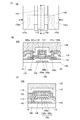
本発明の一態様は、チャネルが形成される層が、バンドギャップの異なる薄膜層を交互に重ねた構造を有する。別言すると、本発明の一態様は、チャネルが形成される層が、バンドギャップの異なる薄膜層を交互に重ねた多層構造を有する。該多層構造は、超格子構造のような構造でもよい。当該構造とすることで、高性能なトランジスタを実現できる。より詳細には、以下の通りである。 One aspect of the present invention has a structure in which the layers on which channels are formed are alternately laminated with thin film layers having different band gaps. In other words, one aspect of the present invention has a multilayer structure in which the layers on which channels are formed are alternately laminated with thin film layers having different band gaps. The multilayer structure may be a structure such as a superlattice structure. With this structure, a high-performance transistor can be realized. More details are as follows.
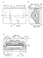
本発明の一態様は、ゲート電極と、第1の導電体と、第2の導電体と、ゲート絶縁体と、金属酸化物を有し、ゲート絶縁体は、ゲート電極と金属酸化物との間に位置し、ゲート電極は、ゲート絶縁体を介して、金属酸化物と重なる領域を有し、第1の導電体および第2の導電体は、金属酸化物の上面および側面と接する領域を有し、金属酸化物は、膜厚方向に第1のバンドギャップを有する酸化物と、第1のバンドギャップを有する酸化物に接する第2のバンドギャップを有する酸化物と、が交互に重なる積層構造を有し、金属酸化物は、第1のバンドギャップを有する酸化物を、2層以上を有し、第1のバンドギャップは、第2のバンドギャップより小さく、第1のバンドギャップを有する酸化物は、In酸化物、Zn酸化物またはIn−Zn酸化物であり、第2のバンドギャップを有する酸化物は、In−M−Zn酸化物(Mはアルミニウム、ガリウム、シリコン、ホウ素、イットリウム、銅、バナジウム、ベリリウム、チタン、鉄、ニッケル、ゲルマニウム、ジルコニウム、モリブデン、ランタン、セリウム、ネオジム、ハフニウム、タンタル、タングステン、またはマグネシウム)であり、第2のバンドギャップを有する酸化物は、In、M、及びZnの原子数の総和に対して、Inの含有量が40%以上50%以下の領域と、Mの含有量が5%以上30%以下の領域と、を有するトランジスタである。 One aspect of the present invention includes a gate electrode, a first conductor, a second conductor, a gate insulator, and a metal oxide, and the gate insulator comprises a gate electrode and a metal oxide. Located in between, the gate electrode has a region that overlaps the metal oxide via the gate insulator, and the first conductor and the second conductor have regions that are in contact with the upper surface and the side surface of the metal oxide. The metal oxide is a laminate in which an oxide having a first band gap in the film thickness direction and an oxide having a second band gap in contact with an oxide having a first band gap are alternately overlapped. Having a structure, the metal oxide has two or more layers of oxide having a first band gap, the first band gap is smaller than the second band gap, and has a first band gap. The oxide is an In oxide, a Zn oxide or an In-Zn oxide, and the oxide having a second band gap is an In-M-Zn oxide (M is aluminum, gallium, silicon, boron, yttrium). , Copper, vanadium, berylium, titanium, iron, nickel, germanium, zirconium, molybdenum, lantern, cerium, neodymium, hafnium, tantalum, tungsten, or magnesium), and oxides with a second band gap are In, A transistor having an In content of 40% or more and 50% or less and a M content of 5% or more and 30% or less with respect to the total number of atoms of M and Zn.
または、本発明の一態様は、ゲート電極と、第1の導電体と、第2の導電体と、ゲート絶縁体と、金属酸化物を有し、ゲート絶縁体は、ゲート電極と金属酸化物との間に位置し、ゲート電極は、ゲート絶縁体を介して、金属酸化物と重なる領域を有し、第1の導電体および第2の導電体は、金属酸化物の上面および側面と接する領域を有し、金属酸化物は、膜厚方向に第1のバンドギャップを有する酸化物と、第1のバンドギャップを有する酸化物に接する第2のバンドギャップを有する酸化物と、が交互に重なる積層構造を有し、金属酸化物は、第1のバンドギャップを有する酸化物を、2層以上を有し、第1のバンドギャップは、第2のバンドギャップより小さく、第2のバンドギャップと第1のバンドギャップの差は、0.1eV以上2.5eV以下、または0.3eV以上1.3eV以下であり、第1のバンドギャップを有する酸化物は、In酸化物、Zn酸化物またはIn−Zn酸化物であり、第2のバンドギャップを有する酸化物は、In−M−Zn酸化物(Mはアルミニウム、ガリウム、シリコン、ホウ素、イットリウム、銅、バナジウム、ベリリウム、チタン、鉄、ニッケル、ゲルマニウム、ジルコニウム、モリブデン、ランタン、セリウム、ネオジム、ハフニウム、タンタル、タングステン、またはマグネシウム)であり、第2のバンドギャップを有する酸化物は、In、M、及びZnの原子数の総和に対して、Inの含有量が40%以上50%以下の領域と、Mの含有量が5%以上30%以下の領域と、を有するトランジスタである。 Alternatively, one aspect of the present invention has a gate electrode, a first conductor, a second conductor, a gate insulator, and a metal oxide, and the gate insulator is a gate electrode and a metal oxide. Located between and, the gate electrode has a region that overlaps the metal oxide via the gate insulator, and the first conductor and the second conductor are in contact with the upper surface and the side surface of the metal oxide. The metal oxide having a region alternates between an oxide having a first band gap in the film thickness direction and an oxide having a second band gap in contact with the oxide having the first band gap. It has an overlapping laminated structure, the metal oxide has two or more layers of oxide having a first band gap, the first band gap is smaller than the second band gap, and the second band gap. The difference between and the first band gap is 0.1 eV or more and 2.5 eV or less, or 0.3 eV or more and 1.3 eV or less, and the oxide having the first band gap is In oxide, Zn oxide or The In-Zn oxide, which has a second band gap, is an In-M-Zn oxide (M is aluminum, gallium, silicon, boron, yttrium, copper, vanadium, beryllium, titanium, iron, nickel). , Germanium, zirconium, molybdenum, lanthanum, cerium, neodymium, hafnium, tantalum, tungsten, or magnesium), and oxides with a second band gap are relative to the total number of atoms of In, M, and Zn. , A transistor having an In content of 40% or more and 50% or less, and an M content of 5% or more and 30% or less.
または、本発明の一態様は、ゲート電極と、第1の導電体と、第2の導電体と、ゲート絶縁体と、金属酸化物を有し、ゲート絶縁体は、ゲート電極と金属酸化物との間に位置し、ゲート電極は、ゲート絶縁体を介して、金属酸化物と重なる領域を有し、第1の導電体および第2の導電体は、金属酸化物の上面および側面と接する領域を有し、金属酸化物は、膜厚方向に第1のバンドギャップを有する酸化物と、第1のバンドギャップを有する酸化物に接する第2のバンドギャップを有する酸化物と、が交互に重なる積層構造を有し、金属酸化物は、第1のバンドギャップを有する酸化物を、2層以上を有し、第1のバンドギャップは、第2のバンドギャップより小さく、第2のバンドギャップを有する酸化物の伝導帯下端と第1のバンドギャップを有する酸化物の伝導帯下端の差は、0.1eV以上1.3eV以下、または0.3eV以上1.3eV以下であり、第1のバンドギャップを有する酸化物は、In酸化物、Zn酸化物またはIn−Zn酸化物であり、第2のバンドギャップを有する酸化物は、In−M−Zn酸化物(Mはアルミニウム、ガリウム、シリコン、ホウ素、イットリウム、銅、バナジウム、ベリリウム、チタン、鉄、ニッケル、ゲルマニウム、ジルコニウム、モリブデン、ランタン、セリウム、ネオジム、ハフニウム、タンタル、タングステン、またはマグネシウム)であり、第2のバンドギャップを有する酸化物は、In、M、及びZnの原子数の総和に対して、Inの含有量が40%以上50%以下の領域と、Mの含有量が5%以上30%以下の領域と、を有するトランジスタである。 Alternatively, one aspect of the present invention has a gate electrode, a first conductor, a second conductor, a gate insulator, and a metal oxide, and the gate insulator is a gate electrode and a metal oxide. Located between and, the gate electrode has a region that overlaps the metal oxide via the gate insulator, and the first conductor and the second conductor are in contact with the upper surface and the side surface of the metal oxide. The metal oxide having a region alternates between an oxide having a first band gap in the film thickness direction and an oxide having a second band gap in contact with the oxide having the first band gap. It has an overlapping laminated structure, the metal oxide has two or more layers of oxide having a first band gap, the first band gap is smaller than the second band gap, and the second band gap. The difference between the lower end of the conduction band of the oxide having the above and the lower end of the conduction band of the oxide having the first band gap is 0.1 eV or more and 1.3 eV or less, or 0.3 eV or more and 1.3 eV or less, and the first The oxide having a band gap is an In oxide, Zn oxide or In-Zn oxide, and the oxide having a second band gap is an In-M-Zn oxide (M is aluminum, gallium, silicon). , Boron, ittrium, copper, vanadium, beryllium, titanium, iron, nickel, germanium, zirconium, molybdenum, lanthanum, cerium, neodymium, hafnium, tantalum, tungsten, or magnesium) Is a transistor having an In content of 40% or more and 50% or less and a M content of 5% or more and 30% or less with respect to the total number of atoms of In, M, and Zn. Is.
または、本発明の一態様は、ゲート電極と、第1の導電体と、第2の導電体と、ゲート絶縁体と、金属酸化物を有し、ゲート絶縁体は、ゲート電極と金属酸化物との間に位置し、ゲート電極は、ゲート絶縁体を介して、金属酸化物と重なる領域を有し、第1の導電体および第2の導電体は、金属酸化物の上面および側面と接する領域を有し、金属酸化物は、膜厚方向に第1のバンドギャップを有する酸化物と、第1のバンドギャップを有する酸化物に接する第2のバンドギャップを有する酸化物と、が交互に重なる積層構造を有し、金属酸化物は、第1のバンドギャップを有する酸化物を、2層以上を有し、第1のバンドギャップは、前記第2のバンドギャップより小さく、ゲート電圧が0Vを保持した状態において、第2のバンドギャップを有する酸化物の伝導帯下端とフェルミレベルとの差は、第1のバンドギャップを有する酸化物の伝導帯下端とフェルミレベルとの差より大きく、第1のバンドギャップを有する酸化物は、In酸化物、Zn酸化物またはIn−Zn酸化物であり、第2のバンドギャップを有する酸化物は、In−M−Zn酸化物(Mはアルミニウム、ガリウム、シリコン、ホウ素、イットリウム、銅、バナジウム、ベリリウム、チタン、鉄、ニッケル、ゲルマニウム、ジルコニウム、モリブデン、ランタン、セリウム、ネオジム、ハフニウム、タンタル、タングステン、またはマグネシウム)であり、第2のバンドギャップを有する酸化物は、In、M、及びZnの原子数の総和に対して、Inの含有量が40%以上50%以下の領域と、Mの含有量が5%以上30%以下の領域と、を有するトランジスタである。 Alternatively, one aspect of the present invention has a gate electrode, a first conductor, a second conductor, a gate insulator, and a metal oxide, and the gate insulator is a gate electrode and a metal oxide. Located between and, the gate electrode has a region that overlaps the metal oxide via the gate insulator, and the first conductor and the second conductor are in contact with the upper surface and the side surface of the metal oxide. The metal oxide having a region alternates between an oxide having a first band gap in the film thickness direction and an oxide having a second band gap in contact with the oxide having the first band gap. It has an overlapping laminated structure, the metal oxide has two or more layers of oxide having a first band gap, the first band gap is smaller than the second band gap, and the gate voltage is 0 V. The difference between the lower end of the conduction band of the oxide having the second band gap and the Fermi level is larger than the difference between the lower end of the conduction band of the oxide having the first band gap and the Fermi level. The oxide having a band gap of 1 is an In oxide, Zn oxide or In—Zn oxide, and the oxide having a second band gap is an In—M—Zn oxide (M is aluminum, gallium). , Silicon, boron, yttrium, copper, vanadium, beryllium, titanium, iron, nickel, germanium, zirconium, molybdenum, lanthanum, cerium, neodymium, hafnium, tantalum, tungsten, or magnesium) and has a second band gap. The oxide contains a region in which the In content is 40% or more and 50% or less and a region in which the M content is 5% or more and 30% or less with respect to the total number of atoms of In, M, and Zn. It is a transistor to have.
また、上記態様において、金属酸化物は、第1のバンドギャップを有する酸化物を、3層以上10層以下を有してもよい。 Further, in the above aspect, the metal oxide may have an oxide having a first bandgap of 3 layers or more and 10 layers or less.
または、本発明の一態様は、ゲート電極と、第1の導電体と、第2の導電体と、ゲート絶縁体と、第1の金属酸化物と、第2の金属酸化物と、第3の金属酸化物を有し、ゲート絶縁体は、ゲート電極と第1の金属酸化物との間に位置し、ゲート電極は、ゲート絶縁体および第1の金属酸化物を介して、第2の金属酸化物と重なる領域を有し、第1の導電体および第2の導電体は、第2の金属酸化物の上面および側面と接する領域を有し、第2の金属酸化物は、第3の金属酸化物の上面と接する領域を有し、第2の金属酸化物は、膜厚方向に第1のバンドギャップを有する酸化物と、第1のバンドギャップを有する酸化物に接する第2のバンドギャップを有する酸化物と、が交互に重なる積層構造を有し、第2の酸化物は、第1のバンドギャップを有する酸化物を、2層以上を有し、第1のバンドギャップは、第2のバンドギャップより小さく、第2のバンドギャップと第1のバンドギャップの差は、0.1eV以上2.5eV以下、または0.3eV以上1.3eV以下であり、第1のバンドギャップを有する酸化物は、In酸化物、Zn酸化物またはIn−Zn酸化物であり、第2のバンドギャップを有する酸化物は、In−M−Zn酸化物(Mはアルミニウム、ガリウム、シリコン、ホウ素、イットリウム、銅、バナジウム、ベリリウム、チタン、鉄、ニッケル、ゲルマニウム、ジルコニウム、モリブデン、ランタン、セリウム、ネオジム、ハフニウム、タンタル、タングステン、またはマグネシウム)であり、第2のバンドギャップを有する酸化物は、In、M、及びZnの原子数の総和に対して、Inの含有量が40%以上50%以下の領域と、Mの含有量が5%以上30%以下の領域と、を有するトランジスタである。 Alternatively, one aspect of the present invention includes a gate electrode, a first conductor, a second conductor, a gate insulator, a first metal oxide, a second metal oxide, and a third. The gate insulator is located between the gate electrode and the first metal oxide, and the gate electrode has a second metal oxide via the gate insulator and the first metal oxide. The first conductor and the second conductor have a region in contact with the upper surface and the side surface of the second metal oxide, and the second metal oxide has a region in contact with the upper surface and the side surface of the second metal oxide. The second metal oxide has a region in contact with the upper surface of the metal oxide of the above, and the second metal oxide is in contact with an oxide having a first band gap in the film thickness direction and an oxide having a first band gap. It has a laminated structure in which oxides having band gaps are alternately overlapped, the second oxide has two or more layers of oxides having a first band gap, and the first band gap is Smaller than the second band gap, the difference between the second band gap and the first band gap is 0.1 eV or more and 2.5 eV or less, or 0.3 eV or more and 1.3 eV or less, and the first band gap is set. The oxide having an oxide is an In oxide, a Zn oxide or an In-Zn oxide, and the oxide having a second band gap is an In-M-Zn oxide (M is aluminum, gallium, silicon, boron, Ittrium, copper, vanadium, beryllium, titanium, iron, nickel, germanium, zirconium, molybdenum, lanthanum, cerium, neodymium, hafnium, tantalum, tungsten, or magnesium), and the oxide having the second band gap is In. A transistor having an In content of 40% or more and 50% or less and a M content of 5% or more and 30% or less with respect to the total number of atoms of M, M, and Zn.
また、上記態様において、第2の金属酸化物は、チャネル形成領域を有し、チャネル形成領域のチャネル幅方向において、第1の金属酸化物は、第2の金属酸化物を覆う様に配されていてもよい。 Further, in the above aspect, the second metal oxide has a channel forming region, and the first metal oxide is arranged so as to cover the second metal oxide in the channel width direction of the channel forming region. You may be.
また、上記態様において、第2の金属酸化物は、第1のバンドギャップを有する酸化物を、3層以上10層以下を有してもよい。 Further, in the above aspect, the second metal oxide may have an oxide having a first bandgap of 3 layers or more and 10 layers or less.
また、上記態様において、第1の金属酸化物のバンドギャップおよび第3の金属酸化物のバンドギャップは、第2の金属酸化物のバンドギャップより大きくてもよい。 Further, in the above embodiment, the band gap of the first metal oxide and the band gap of the third metal oxide may be larger than the band gap of the second metal oxide.
また、上記態様において、第1のバンドギャップを有する酸化物の膜厚は、0.5nm以上10nm以下の領域、または0.5nm以上2.0nm以下の領域を有してもよい。 Further, in the above aspect, the film thickness of the oxide having the first band gap may have a region of 0.5 nm or more and 10 nm or less, or a region of 0.5 nm or more and 2.0 nm or less.
また、上記態様において、第2のバンドギャップを有する酸化物の膜厚は、0.1nm以上10nm以下の領域、または0.1nm以上3.0nm以下の領域を有してもよい。 Further, in the above aspect, the film thickness of the oxide having the second band gap may have a region of 0.1 nm or more and 10 nm or less, or a region of 0.1 nm or more and 3.0 nm or less.
また、上記態様において、第1の導電体の端部と第2の導電体の端部との互いに向かい合う距離は、10nm以上300nm以下の領域を有してもよい。 Further, in the above aspect, the distance between the end portion of the first conductor and the end portion of the second conductor facing each other may have a region of 10 nm or more and 300 nm or less.
また、上記態様において、ゲート電極の幅は、10nm以上300nm以下の領域を有してもよい。 Further, in the above aspect, the width of the gate electrode may have a region of 10 nm or more and 300 nm or less.
また、上記態様において、第1のバンドギャップを有する酸化物のキャリア密度は、6×1018cm−3以上5×1020cm−3以下であってもよい。 Further, in the above embodiment, the carrier density of the oxide having the first bandgap may be 6 × 10 18 cm -3 or more and 5 × 10 20 cm -3 or less.
また、上記態様において、第1のバンドギャップを有する酸化物は、縮退してもよい。 Further, in the above aspect, the oxide having the first bandgap may be degenerated.
また、上記態様において、第1のバンドギャップを有する酸化物は、インジウム及び亜鉛の一方または双方を有してもよい。 Further, in the above embodiment, the oxide having the first bandgap may have one or both of indium and zinc.
また、上記態様において、第2のバンドギャップを有する酸化物は、In、M、及びZnの原子数の総和に対して、Inの原子数比が4の場合、Mの原子数比が1.5以上2.5以下であり、且つZnの原子数比が2以上4以下である領域を有し、代表的には、In、M、及びZnの原子数比は、In:M:Zn=4:2:3近傍であってもよい。 Further, in the above embodiment, when the atomic number ratio of In is 4 with respect to the total atomic number of In, M, and Zn, the oxide having the second band gap has an atomic number ratio of M of 1. It has a region of 5 or more and 2.5 or less and the atomic number ratio of Zn is 2 or more and 4 or less, and typically, the atomic number ratio of In, M, and Zn is In: M: Zn =. It may be in the vicinity of 4: 2: 3.
また、上記態様において、第2のバンドギャップを有する酸化物は、In、M、及びZnの原子数の総和に対して、Inの原子数比が5の場合、Mの原子数比が0.5以上1.5以下であり、且つ前記Znの原子数比が5以上7以下である領域を有し、代表的には、In、M、及びZnの原子数比は、In:M:Zn=5:1:6近傍であってもよい。 Further, in the above embodiment, when the atomic number ratio of In is 5 with respect to the total atomic number of In, M, and Zn, the oxide having the second band gap has an atomic number ratio of M of 0. It has a region in which the atomic number ratio of Zn is 5 or more and 1.5 or less and the atomic number ratio of Zn is 5 or more and 7 or less, and typically, the atomic number ratio of In, M, and Zn is In: M: Zn. = It may be in the vicinity of 5: 1: 6.
本発明の一態様により、良好な電気特性を有する半導体装置を提供できる。または、本発明の一態様により、微細化または高集積化が可能な半導体装置を提供できる。または、本発明の一態様により、生産性の高い半導体装置を提供できる。 According to one aspect of the present invention, a semiconductor device having good electrical characteristics can be provided. Alternatively, one aspect of the present invention can provide a semiconductor device capable of miniaturization or high integration. Alternatively, one aspect of the present invention can provide a highly productive semiconductor device.
または、本発明の一態様により、長期間においてデータの保持が可能な半導体装置を提供できる。または、本発明の一態様により、情報の書き込み速度が速い半導体装置を提供できる。または、本発明の一態様により、設計自由度が高い半導体装置を提供できる。または、本発明の一態様により、消費電力を抑えることができる半導体装置を提供できる。または、本発明の一態様により、新規な半導体装置を提供できる。 Alternatively, one aspect of the present invention can provide a semiconductor device capable of retaining data for a long period of time. Alternatively, according to one aspect of the present invention, it is possible to provide a semiconductor device having a high information writing speed. Alternatively, one aspect of the present invention can provide a semiconductor device having a high degree of freedom in design. Alternatively, according to one aspect of the present invention, it is possible to provide a semiconductor device capable of suppressing power consumption. Alternatively, one aspect of the present invention can provide a novel semiconductor device.
なお、これらの効果の記載は、他の効果の存在を妨げるものではない。なお、本発明の一態様は、これらの効果の全てを有する必要はない。なお、これら以外の効果は、明細書、図面、請求項などの記載から、自ずと明らかとなるものであり、明細書、図面、請求項などの記載から、これら以外の効果を抽出することが可能である。 The description of these effects does not preclude the existence of other effects. It should be noted that one aspect of the present invention does not have to have all of these effects. It should be noted that the effects other than these are naturally clarified from the description of the description, drawings, claims, etc., and it is possible to extract the effects other than these from the description of the description, drawings, claims, etc. Is.
以下、実施の形態について図面を参照しながら説明する。但し、実施の形態は多くの異なる態様で実施することが可能であり、趣旨およびその範囲から逸脱することなくその形態および詳細を様々に変更し得ることは当業者であれば容易に理解される。従って、本発明は、以下の実施の形態の記載内容に限定して解釈されるものではない。 Hereinafter, embodiments will be described with reference to the drawings. However, it is easily understood by those skilled in the art that the embodiments can be implemented in many different embodiments and that the embodiments and details can be variously modified without departing from the spirit and scope thereof. .. Therefore, the present invention is not construed as being limited to the description of the following embodiments.
また、図面において、大きさ、層の厚さ、又は領域は、明瞭化のために誇張されている場合がある。よって、必ずしもそのスケールに限定されない。なお図面は、理想的な例を模式的に示したものであり、図面に示す形状又は値などに限定されない。また、図面において、同一部分又は同様な機能を有する部分には同一の符号を異なる図面間で共通して用い、その繰り返しの説明は省略する。また、同様の機能を指す場合には、ハッチパターンを同じくし、特に符号を付さない場合がある。 Also, in the drawings, the size, layer thickness, or area may be exaggerated for clarity. Therefore, it is not necessarily limited to that scale. The drawings schematically show ideal examples, and are not limited to the shapes or values shown in the drawings. Further, in the drawings, the same reference numerals are commonly used between different drawings for the same parts or parts having similar functions, and the repeated description thereof will be omitted. Further, when referring to the same function, the hatch pattern may be the same and no particular sign may be added.
また、本明細書などにおいて、第1、第2等として付される序数詞は便宜上用いるものであり、工程順又は積層順を示すものではない。そのため、例えば、「第1の」を「第2の」又は「第3の」などと適宜置き換えて説明することができる。また、本明細書等に記載されている序数詞と、本発明の一態様を特定するために用いられる序数詞は一致しない場合がある。 Further, in the present specification and the like, the ordinal numbers attached as the first, second and the like are used for convenience and do not indicate the process order or the stacking order. Therefore, for example, the "first" can be appropriately replaced with the "second" or "third" for explanation. In addition, the ordinal numbers described in the present specification and the like may not match the ordinal numbers used to specify one aspect of the present invention.
また、本明細書において、「上に」、「下に」などの配置を示す語句は、構成同士の位置関係を、図面を参照して説明するために、便宜上用いている。また、構成同士の位置関係は、各構成を描写する方向に応じて適宜変化するものである。従って、明細書で説明した語句に限定されず、状況に応じて適切に言い換えることができる。 Further, in the present specification, terms indicating the arrangement such as "above" and "below" are used for convenience in order to explain the positional relationship between the configurations with reference to the drawings. Further, the positional relationship between the configurations changes as appropriate according to the direction in which each configuration is depicted. Therefore, it is not limited to the words and phrases explained in the specification, and can be appropriately paraphrased according to the situation.
また、本明細書等において、半導体装置とは、半導体特性を利用することで機能しうる装置全般を指す。トランジスタなどの半導体素子をはじめ、半導体回路、演算装置、記憶装置は、半導体装置の一態様である。撮像装置、表示装置、液晶表示装置、発光装置、電気光学装置、発電装置(薄膜太陽電池、有機薄膜太陽電池等を含む)、および電子機器は、半導体装置を有する場合がある。 Further, in the present specification and the like, the semiconductor device refers to all devices that can function by utilizing the semiconductor characteristics. A semiconductor device such as a transistor, a semiconductor circuit, an arithmetic unit, and a storage device are one aspect of the semiconductor device. An image pickup device, a display device, a liquid crystal display device, a light emitting device, an electro-optical device, a power generation device (including a thin-film solar cell, an organic thin-film solar cell, etc.), and an electronic device may have a semiconductor device.
また、本明細書等において、トランジスタとは、ゲートと、ドレインと、ソースとを含む少なくとも三つの端子を有する素子である。そして、ドレイン(ドレイン端子、ドレイン領域またはドレイン電極)とソース(ソース端子、ソース領域またはソース電極)の間にチャネル形成領域を有しており、チャネル形成領域を介して、ソースとドレインとの間に電流を流すことができるものである。なお、本明細書等において、チャネル形成領域とは、電流が主として流れる領域をいう。 Further, in the present specification and the like, a transistor is an element having at least three terminals including a gate, a drain, and a source. Then, a channel forming region is provided between the drain (drain terminal, drain region or drain electrode) and the source (source terminal, source region or source electrode), and between the source and drain via the channel forming region. It is possible to pass an electric current through. In the present specification and the like, the channel forming region means a region in which a current mainly flows.
また、ソースやドレインの機能は、異なる極性のトランジスタを採用する場合や、回路動作において電流の方向が変化する場合などには入れ替わることがある。このため、本明細書等においては、ソースやドレインの用語は、入れ替えて用いることができるものとする。 Further, the functions of the source and the drain may be interchanged when transistors having different polarities are adopted or when the direction of the current changes in the circuit operation. Therefore, in the present specification and the like, the terms source and drain can be used interchangeably.
なお、本明細書等において、酸化窒化シリコン膜とは、その組成として、窒素よりも酸素の含有量が多いものであって、好ましくは酸素が55原子%以上65原子%以下、窒素が1原子%以上20原子%以下、シリコンが25原子%以上35原子%以下、水素が0.1原子%以上10原子%以下の濃度範囲で含まれるものをいう。また、窒化酸化シリコン膜とは、その組成として、酸素よりも窒素の含有量が多いものであって、好ましくは窒素が55原子%以上65原子%以下、酸素が1原子%以上20原子%以下、シリコンが25原子%以上35原子%以下、水素が0.1原子%以上10原子%以下の濃度範囲で含まれるものをいう。 In the present specification and the like, the silicon oxide film has a composition having a higher oxygen content than nitrogen, preferably 55 atomic% or more and 65 atomic% or less of oxygen, and 1 atom of nitrogen. % Or more and 20 atomic% or less, silicon is 25 atomic% or more and 35 atomic% or less, and hydrogen is 0.1 atomic% or more and 10 atomic% or less. The silicon nitride film has a composition having a higher nitrogen content than oxygen, preferably 55 atomic% or more and 65 atomic% or less of nitrogen, and 1 atomic% or more and 20 atomic% or less of oxygen. , Silicon is contained in a concentration range of 25 atomic% or more and 35 atomic% or less, and hydrogen is contained in a concentration range of 0.1 atomic% or more and 10 atomic% or less.
また、本明細書等において、「膜」という用語と、「層」という用語とは、互いに入れ替えることが可能である。例えば、「導電層」という用語を、「導電膜」という用語に変更することが可能な場合がある。または、例えば、「絶縁膜」という用語を、「絶縁層」という用語に変更することが可能な場合がある。 Further, in the present specification and the like, the term "membrane" and the term "layer" can be interchanged with each other. For example, it may be possible to change the term "conductive layer" to the term "conductive layer". Alternatively, for example, it may be possible to change the term "insulating film" to the term "insulating layer".
また、本明細書等において、「平行」とは、二つの直線が−10°以上10°以下の角度で配置されている状態をいう。したがって、−5°以上5°以下の場合も含まれる。また、「略平行」とは、二つの直線が−30°以上30°以下の角度で配置されている状態をいう。また、「垂直」とは、二つの直線が80°以上100°以下の角度で配置されている状態をいう。したがって、85°以上95°以下の場合も含まれる。また、「略垂直」とは、二つの直線が60°以上120°以下の角度で配置されている状態をいう。 Further, in the present specification and the like, "parallel" means a state in which two straight lines are arranged at an angle of −10 ° or more and 10 ° or less. Therefore, the case of −5 ° or more and 5 ° or less is also included. Further, "substantially parallel" means a state in which two straight lines are arranged at an angle of −30 ° or more and 30 ° or less. Further, "vertical" means a state in which two straight lines are arranged at an angle of 80 ° or more and 100 ° or less. Therefore, the case of 85 ° or more and 95 ° or less is also included. Further, "substantially vertical" means a state in which two straight lines are arranged at an angle of 60 ° or more and 120 ° or less.
また、本明細書において、結晶が三方晶または菱面体晶である場合、六方晶系として表す。 Further, in the present specification, when the crystal is a trigonal crystal or a rhombohedral crystal, it is represented as a hexagonal system.
例えば、本明細書等において、XとYとが接続されている、と明示的に記載されている場合は、XとYとが電気的に接続されている場合と、XとYとが機能的に接続されている場合と、XとYとが直接接続されている場合とが、本明細書等に開示されているものとする。したがって、所定の接続関係、例えば、図または文章に示された接続関係に限定されず、図または文章に示された接続関係以外のものも、図または文章に記載されているものとする。 For example, in the present specification and the like, when it is explicitly stated that X and Y are connected, the case where X and Y are electrically connected and the case where X and Y function. It is assumed that the case where X and Y are directly connected and the case where X and Y are directly connected are disclosed in the present specification and the like. Therefore, the connection relationship is not limited to the predetermined connection relationship, for example, the connection relationship shown in the figure or text, and other than the connection relationship shown in the figure or sentence, it is assumed that the connection relationship is also described in the figure or sentence.
ここで、X、Yは、対象物(例えば、装置、素子、回路、配線、電極、端子、導電膜、層、など)であるとする。 Here, X and Y are assumed to be objects (for example, devices, elements, circuits, wirings, electrodes, terminals, conductive films, layers, etc.).
XとYとが直接的に接続されている場合の一例としては、XとYとの電気的な接続を可能とする素子(例えば、スイッチ、トランジスタ、容量素子、インダクタ、抵抗素子、ダイオード、表示素子、発光素子、負荷など)が、XとYとの間に接続されていない場合であり、XとYとの電気的な接続を可能とする素子(例えば、スイッチ、トランジスタ、容量素子、インダクタ、抵抗素子、ダイオード、表示素子、発光素子、負荷など)を介さずに、XとYとが、接続されている場合である。 As an example of the case where X and Y are directly connected, an element (for example, a switch, a transistor, a capacitive element, an inductor, a resistance element, a diode, a display) that enables an electrical connection between X and Y is used. Elements (eg, switches, transistors, capacitive elements, inductors) that allow an electrical connection between X and Y when the element, light emitting element, load, etc. are not connected between X and Y. , A resistor element, a diode, a display element, a light emitting element, a load, etc.), and X and Y are connected to each other.
XとYとが電気的に接続されている場合の一例としては、XとYとの電気的な接続を可能とする素子(例えば、スイッチ、トランジスタ、容量素子、インダクタ、抵抗素子、ダイオード、表示素子、発光素子、負荷など)が、XとYとの間に1個以上接続されることが可能である。なお、スイッチは、オンオフが制御される機能を有している。つまり、スイッチは、導通状態(オン状態)、または、非導通状態(オフ状態)になり、電流を流すか流さないかを制御する機能を有している。または、スイッチは、電流を流す経路を選択して切り替える機能を有している。なお、XとYとが電気的に接続されている場合は、XとYとが直接的に接続されている場合を含むものとする。 As an example of the case where X and Y are electrically connected, an element (for example, a switch, a transistor, a capacitive element, an inductor, a resistance element, a diode, a display) that enables an electrical connection between X and Y is used. One or more elements, light emitting elements, loads, etc.) can be connected between X and Y. The switch has a function of controlling on / off. That is, the switch is in a conducting state (on state) or a non-conducting state (off state), and has a function of controlling whether or not a current flows. Alternatively, the switch has a function of selecting and switching the path through which the current flows. The case where X and Y are electrically connected includes the case where X and Y are directly connected.
XとYとが機能的に接続されている場合の一例としては、XとYとの機能的な接続を可能とする回路(例えば、論理回路(インバータ、NAND回路、NOR回路など)、信号変換回路(DA変換回路、AD変換回路、ガンマ補正回路など)、電位レベル変換回路(電源回路(昇圧回路、降圧回路など)、信号の電位レベルを変えるレベルシフタ回路など)、電圧源、電流源、切り替え回路、増幅回路(信号振幅または電流量などを大きく出来る回路、オペアンプ、差動増幅回路、ソースフォロワ回路、バッファ回路など)、信号生成回路、記憶回路、制御回路など)が、XとYとの間に1個以上接続されることが可能である。なお、一例として、XとYとの間に別の回路を挟んでいても、Xから出力された信号がYへ伝達される場合は、XとYとは機能的に接続されているものとする。なお、XとYとが機能的に接続されている場合は、XとYとが直接的に接続されている場合と、XとYとが電気的に接続されている場合とを含むものとする。 As an example of the case where X and Y are functionally connected, a circuit that enables functional connection between X and Y (for example, a logic circuit (inverter, NAND circuit, NOR circuit, etc.), signal conversion, etc.) Circuits (DA conversion circuit, AD conversion circuit, gamma correction circuit, etc.), potential level conversion circuit (power supply circuit (boost circuit, step-down circuit, etc.), level shifter circuit that changes the signal potential level, etc.), voltage source, current source, switching Circuits, amplification circuits (circuits that can increase signal amplitude or current amount, operational amplifiers, differential amplification circuits, source follower circuits, buffer circuits, etc.), signal generation circuits, storage circuits, control circuits, etc.) are X and Y. One or more can be connected between them. As an example, even if another circuit is sandwiched between X and Y, if the signal output from X is transmitted to Y, it is assumed that X and Y are functionally connected. To do. When X and Y are functionally connected, it includes a case where X and Y are directly connected and a case where X and Y are electrically connected.
なお、XとYとが電気的に接続されている、と明示的に記載されている場合は、XとYとが電気的に接続されている場合(つまり、XとYとの間に別の素子又は別の回路を挟んで接続されている場合)と、XとYとが機能的に接続されている場合(つまり、XとYとの間に別の回路を挟んで機能的に接続されている場合)と、XとYとが直接接続されている場合(つまり、XとYとの間に別の素子又は別の回路を挟まずに接続されている場合)とが、本明細書等に開示されているものとする。つまり、電気的に接続されている、と明示的に記載されている場合は、単に、接続されている、とのみ明示的に記載されている場合と同様な内容が、本明細書等に開示されているものとする。 When it is explicitly stated that X and Y are electrically connected, it is different when X and Y are electrically connected (that is, between X and Y). When X and Y are functionally connected (that is, when they are connected by sandwiching another circuit between X and Y) and when they are functionally connected by sandwiching another circuit between X and Y. When X and Y are directly connected (that is, when another element or another circuit is not sandwiched between X and Y). It shall be disclosed in documents, etc. That is, when it is explicitly stated that it is electrically connected, the same contents as when it is explicitly stated that it is simply connected are disclosed in the present specification and the like. It is assumed that it has been done.
なお、例えば、トランジスタのソース(又は第1の端子など)が、Z1を介して(又は介さず)、Xと電気的に接続され、トランジスタのドレイン(又は第2の端子など)が、Z2を介して(又は介さず)、Yと電気的に接続されている場合や、トランジスタのソース(又は第1の端子など)が、Z1の一部と直接的に接続され、Z1の別の一部がXと直接的に接続され、トランジスタのドレイン(又は第2の端子など)が、Z2の一部と直接的に接続され、Z2の別の一部がYと直接的に接続されている場合では、以下のように表現することが出来る。 Note that, for example, the source (or first terminal, etc.) of the transistor is electrically connected to X via (or not) Z1, and the drain (or second terminal, etc.) of the transistor connects Z2. When (or not) electrically connected to Y, or the source of the transistor (or the first terminal, etc.) is directly connected to one part of Z1 and another part of Z1. Is directly connected to X, the drain of the transistor (or the second terminal, etc.) is directly connected to one part of Z2, and another part of Z2 is directly connected to Y. Then, it can be expressed as follows.
例えば、「XとYとトランジスタのソース(又は第1の端子など)とドレイン(又は第2の端子など)とは、互いに電気的に接続されており、X、トランジスタのソース(又は第1の端子など)、トランジスタのドレイン(又は第2の端子など)、Yの順序で電気的に接続されている。」と表現することができる。または、「トランジスタのソース(又は第1の端子など)は、Xと電気的に接続され、トランジスタのドレイン(又は第2の端子など)はYと電気的に接続され、X、トランジスタのソース(又は第1の端子など)、トランジスタのドレイン(又は第2の端子など)、Yは、この順序で電気的に接続されている」と表現することができる。または、「Xは、トランジスタのソース(又は第1の端子など)とドレイン(又は第2の端子など)とを介して、Yと電気的に接続され、X、トランジスタのソース(又は第1の端子など)、トランジスタのドレイン(又は第2の端子など)、Yは、この接続順序で設けられている」と表現することができる。これらの例と同様な表現方法を用いて、回路構成における接続の順序について規定することにより、トランジスタのソース(又は第1の端子など)と、ドレイン(又は第2の端子など)とを、区別して、技術的範囲を決定することができる。 For example, "X and Y, the source (or the first terminal, etc.) and the drain (or the second terminal, etc.) of the transistor are electrically connected to each other, and the X, the source of the transistor (or the first terminal, etc.) (Terminals, etc.), transistor drains (or second terminals, etc.), and Y are electrically connected in this order. " Alternatively, "the source of the transistor (or the first terminal, etc.) is electrically connected to X, the drain of the transistor (or the second terminal, etc.) is electrically connected to Y, and the X, the source of the transistor (such as the second terminal). Or the first terminal, etc.), the drain of the transistor (or the second terminal, etc.), and Y are electrically connected in this order. " Alternatively, "X is electrically connected to Y via the source (or first terminal, etc.) and drain (or second terminal, etc.) of the transistor, and X, the source (or first terminal, etc.) of the transistor. (Terminals, etc.), transistor drains (or second terminals, etc.), and Y are provided in this connection order. " By defining the order of connections in the circuit configuration using the same representation method as these examples, the source (or first terminal, etc.) and drain (or second terminal, etc.) of the transistor can be separated. Separately, the technical scope can be determined.
または、別の表現方法として、例えば、「トランジスタのソース(又は第1の端子など)は、少なくとも第1の接続経路を介して、Xと電気的に接続され、前記第1の接続経路は、第2の接続経路を有しておらず、前記第2の接続経路は、トランジスタを介した、トランジスタのソース(又は第1の端子など)とトランジスタのドレイン(又は第2の端子など)との間の経路であり、前記第1の接続経路は、Z1を介した経路であり、トランジスタのドレイン(又は第2の端子など)は、少なくとも第3の接続経路を介して、Yと電気的に接続され、前記第3の接続経路は、前記第2の接続経路を有しておらず、前記第3の接続経路は、Z2を介した経路である。」と表現することができる。または、「トランジスタのソース(又は第1の端子など)は、少なくとも第1の接続経路によって、Z1を介して、Xと電気的に接続され、前記第1の接続経路は、第2の接続経路を有しておらず、前記第2の接続経路は、トランジスタを介した接続経路を有し、トランジスタのドレイン(又は第2の端子など)は、少なくとも第3の接続経路によって、Z2を介して、Yと電気的に接続され、前記第3の接続経路は、前記第2の接続経路を有していない。」と表現することができる。または、「トランジスタのソース(又は第1の端子など)は、少なくとも第1の電気的パスによって、Z1を介して、Xと電気的に接続され、前記第1の電気的パスは、第2の電気的パスを有しておらず、前記第2の電気的パスは、トランジスタのソース(又は第1の端子など)からトランジスタのドレイン(又は第2の端子など)への電気的パスであり、トランジスタのドレイン(又は第2の端子など)は、少なくとも第3の電気的パスによって、Z2を介して、Yと電気的に接続され、前記第3の電気的パスは、第4の電気的パスを有しておらず、前記第4の電気的パスは、トランジスタのドレイン(又は第2の端子など)からトランジスタのソース(又は第1の端子など)への電気的パスである。」と表現することができる。これらの例と同様な表現方法を用いて、回路構成における接続経路について規定することにより、トランジスタのソース(又は第1の端子など)と、ドレイン(又は第2の端子など)とを、区別して、技術的範囲を決定することができる。 Alternatively, as another expression, for example, "the source of the transistor (or the first terminal, etc.) is electrically connected to X via at least the first connection path, and the first connection path is. It does not have a second connection path, and the second connection path is between the source of the transistor (or the first terminal, etc.) and the drain of the transistor (or the second terminal, etc.) via the transistor. The first connection path is a path via Z1, and the drain (or second terminal, etc.) of the transistor is electrically connected to Y via at least a third connection path. It is connected, and the third connection path does not have the second connection path, and the third connection path is a path via Z2. " Alternatively, "the source of the transistor (or the first terminal, etc.) is electrically connected to X via Z1 by at least the first connection path, and the first connection path is the second connection path. The second connection path has a connection path via a transistor, and the drain (or the second terminal, etc.) of the transistor has a connection path via Z2 by at least a third connection path. , Y is electrically connected, and the third connection path does not have the second connection path. " Alternatively, "the source of the transistor (or the first terminal, etc.) is electrically connected to X via Z1 by at least the first electrical path, the first electrical path being the second. It does not have an electrical path, and the second electrical path is an electrical path from the source of the transistor (or the first terminal, etc.) to the drain of the transistor (or the second terminal, etc.). The drain (or second terminal, etc.) of the transistor is electrically connected to Y via Z2 by at least a third electrical path, the third electrical path being a fourth electrical path. The fourth electrical path is an electrical path from the drain of the transistor (or the second terminal, etc.) to the source of the transistor (or the first terminal, etc.). " can do. By defining the connection path in the circuit configuration using the same representation method as these examples, the source (or first terminal, etc.) of the transistor and the drain (or second terminal, etc.) can be distinguished. , The technical scope can be determined.
なお、これらの表現方法は、一例であり、これらの表現方法に限定されない。ここで、X、Y、Z1、Z2は、対象物(例えば、装置、素子、回路、配線、電極、端子、導電膜、層、など)であるとする。 Note that these expression methods are examples, and are not limited to these expression methods. Here, it is assumed that X, Y, Z1 and Z2 are objects (for example, devices, elements, circuits, wirings, electrodes, terminals, conductive films, layers, etc.).
なお、回路図上は独立している構成要素同士が電気的に接続しているように図示されている場合であっても、1つの構成要素が、複数の構成要素の機能を併せ持っている場合もある。例えば配線の一部が電極としても機能する場合は、一の導電膜が、配線の機能、および電極の機能の両方の構成要素の機能を併せ持っている。したがって、本明細書における電気的に接続とは、このような、一の導電膜が、複数の構成要素の機能を併せ持っている場合も、その範疇に含める。 Even if the circuit diagram shows that independent components are electrically connected to each other, one component has the functions of a plurality of components. There is also. For example, when a part of the wiring also functions as an electrode, one conductive film has the functions of both the wiring function and the electrode function. Therefore, the term "electrically connected" as used herein includes the case where one conductive film has the functions of a plurality of components in combination.
なお、本明細書において、バリア膜とは、水素などの不純物および酸素の透過を抑制する機能を有する膜のことであり、該バリア膜に導電性を有する場合は、導電性バリア膜と呼ぶことがある。 In the present specification, the barrier film is a film having a function of suppressing the permeation of impurities such as hydrogen and oxygen, and when the barrier film has conductivity, it is referred to as a conductive barrier film. There is.
本明細書等において、金属酸化物(metal oxide)とは、広い表現での金属の酸化物である。金属酸化物は、酸化物絶縁体、酸化物導電体(透明酸化物導電体を含む)、酸化物半導体(Oxide Semiconductorまたは単にOSともいう)などに分類される。例えば、トランジスタの活性層に金属酸化物を用いた場合、当該金属酸化物を酸化物半導体と呼称する場合がある。つまり、金属酸化物が増幅作用、整流作用、及びスイッチング作用の少なくとも1つを有する場合、当該金属酸化物を、金属酸化物半導体(metal oxide semiconductor)、略してOSと呼ぶことができる。また、OS FETと記載する場合においては、金属酸化物または酸化物半導体を有するトランジスタと換言することができる。 In the present specification and the like, a metal oxide is a metal oxide in a broad expression. Metal oxides are classified into oxide insulators, oxide conductors (including transparent oxide conductors), oxide semiconductors (also referred to as Oxide Semiconductor or simply OS) and the like. For example, when a metal oxide is used in the active layer of a transistor, the metal oxide may be referred to as an oxide semiconductor. That is, when the metal oxide has at least one of an amplification action, a rectifying action, and a switching action, the metal oxide can be referred to as a metal oxide semiconductor, or OS for short. Further, when the term "OS FET" is used, it can be rephrased as a transistor having a metal oxide or an oxide semiconductor.
また、本明細書等において、CAAC(c−axis aligned crystal)、及びCAC(cloud−aligned composite)と記載する場合がある。なお、CAACは結晶構造の一例を表し、CACは機能、または材料の構成の一例を表す。 Further, in the present specification and the like, it may be described as CAAC (c-axis aligned composite) and CAC (cloud-aligned composite). In addition, CAAC represents an example of a crystal structure, and CAC represents an example of a function or a composition of a material.
また、本明細書等において、CAC−OSまたはCAC−metal oxideは、材料の一部では導電体の機能と、材料の一部では誘電体(または絶縁体)の機能とを有し、材料の全体では半導体としての機能を有する。なお、CAC−OSまたはCAC−metal oxideを、トランジスタの半導体層に用いる場合、導電体の領域は、キャリアとなる電子(またはホール)を流す機能を有し、誘電体の領域は、キャリアとなる電子を流さない機能を有する。導電体としての機能と、誘電体としての機能とを、それぞれ相補的に作用させることで、スイッチングさせる機能(On/Offさせる機能)をCAC−OSまたはCAC−metal oxideに付与することができる。CAC−OSまたはCAC−metal oxideにおいて、それぞれの機能を分離させることで、双方の機能を最大限に高めることができる。 Further, in the present specification and the like, CAC-OS or CAC-metal oxide has a function of a conductor in a part of a material and a function of a dielectric (or an insulator) in a part of the material. As a whole, it has a function as a semiconductor. When CAC-OS or CAC-metal oxide is used for the semiconductor layer of the transistor, the conductor region has a function of allowing electrons (or holes) to be carriers to flow, and the dielectric region is a carrier. It has a function of not allowing electrons to flow. By making the function as a conductor and the function as a dielectric act in a complementary manner, a switching function (on / off function) can be imparted to the CAC-OS or the CAC-metric oxide. In CAC-OS or CAC-metal oxide, by separating each function, both functions can be maximized.
また、本明細書等において、CAC−OSまたはCAC−metal oxideは、導電体領域、及び誘電体領域を有する。導電体領域は、上述の導電体の機能を有し、誘電体領域は、上述の誘電体の機能を有する。また、材料中において、導電体領域と、誘電体領域とは、ナノ粒子レベルで分離している場合がある。また、導電体領域と、誘電体領域とは、それぞれ材料中に偏在する場合がある。また、導電体領域は、周辺がぼけてクラウド状に連結して観察される場合がある。 Further, in the present specification and the like, CAC-OS or CAC-metal oxide has a conductor region and a dielectric region. The conductor region has the function of the above-mentioned conductor, and the dielectric region has the function of the above-mentioned dielectric. Further, in the material, the conductor region and the dielectric region may be separated at the nanoparticle level. Further, the conductor region and the dielectric region may be unevenly distributed in the material, respectively. In addition, the conductor region may be observed by being connected in a cloud shape with a blurred periphery.
すなわち、CAC−OSまたはCAC−metal oxideは、マトリックス複合材(matrix composite)、または金属マトリックス複合材(metal matrix composite)と呼称することもできる。 That is, the CAC-OS or CAC-metal oxide can also be referred to as a matrix composite or a metal matrix composite.
また、CAC−OSまたはCAC−metal oxideにおいて、導電体領域と、誘電体領域とは、それぞれ0.5nm以上10nm以下、好ましくは0.5nm以上3nm以下のサイズで材料中に分散している場合がある。 Further, in CAC-OS or CAC-metal oxide, when the conductor region and the dielectric region are dispersed in the material in a size of 0.5 nm or more and 10 nm or less, preferably 0.5 nm or more and 3 nm or less, respectively. There is.
(実施の形態1)
<トランジスタの構成1>
図1(A)は、本発明の一態様であるトランジスタの上面図である。また、図1(B)は、図1(A)にA3−A4の一点鎖線で示す部位の断面図である。つまりトランジスタのチャネル形成領域におけるチャネル幅方向の断面図をしめす。図1(C)は、図1(A)にA1−A2の一点鎖線で示す部位の断面図である。つまりトランジスタのチャネル長方向の断面図をしめす。図1(A)の上面図では、図の明瞭化のために一部の要素を省いて図示している。
(Embodiment 1)
<
FIG. 1A is a top view of a transistor according to an aspect of the present invention. Further, FIG. 1 (B) is a cross-sectional view of a portion shown by a alternate long and short dash line of A3-A4 in FIG. 1 (A). That is, a cross-sectional view in the channel width direction in the channel formation region of the transistor is shown. FIG. 1C is a cross-sectional view of a portion shown by a alternate long and short dash line in A1-A2 in FIG. 1A. That is, a cross-sectional view of the transistor in the channel length direction is shown. In the top view of FIG. 1A, some elements are omitted for the sake of clarity.
図1(B)および(C)において、トランジスタは、基板400上の絶縁体401bに配置される。なお、絶縁体401bは、絶縁体401aを介して基板400に設けられる。トランジスタは、絶縁体301と、絶縁体301が開口部を有していて、開口部内に導電体310が配置され、導電体310および絶縁体301上の絶縁体302と、絶縁体302上の絶縁体303と、絶縁体303上の絶縁体402と、絶縁体402上の酸化物406aと、酸化物406a上の酸化物406bと、酸化物406bの上面および側面と接する領域を有する導電体416a1および導電体416a2と、導電体416a1の側面、導電体416a2の側面および酸化物406bの上面と接する領域を有する酸化物406cと、酸化物406c上の絶縁体412と、酸化物406cと絶縁体412を介して互いに重なる領域を有する導電体404と、を有する。
In FIGS. 1B and 1C, the transistor is arranged on the
また、絶縁体408a、絶縁体408bおよび絶縁体410が、トランジスタ上に設けられる。
Further, an
なお、酸化物406a、酸化物406bおよび酸化物406cはそれぞれ、金属酸化物を用いることができる。
As the
トランジスタにおいて、導電体404は第1のゲート電極としての機能を有する。また、導電体404は、酸素の透過を抑制する機能を有する導電体と積層構造とすることができる。例えば酸素の透過を抑制する機能を有する導電体を下層に成膜することで導電体404の酸化による電気抵抗値の増加を防ぐことができる。絶縁体412は第1のゲート絶縁体としての機能を有する。
In the transistor, the
また、導電体416a1および導電体416a2は、ソース電極またはドレイン電極としての機能を有する。また、導電体416a1および導電体416a2は、酸素の透過を抑制する機能を有する導電体と積層構造とすることができる。例えば酸素の透過を抑制する機能を有する導電体を上層に成膜することで導電体416a1および導電体416a2の酸化による電気抵抗値の増加を防ぐことができる。なお、導電体の電気抵抗値の測定は、2端子法などを用いて測定することができる。 Further, the conductor 416a1 and the conductor 416a2 have a function as a source electrode or a drain electrode. Further, the conductor 416a1 and the conductor 416a2 can have a laminated structure with the conductor having a function of suppressing the permeation of oxygen. For example, by forming a conductor having a function of suppressing the permeation of oxygen on the upper layer, it is possible to prevent an increase in the electric resistance value due to oxidation of the conductors 416a1 and 416a2. The electric resistance value of the conductor can be measured by using a two-terminal method or the like.
また、導電体416a1の上面に接してバリア膜417a1が配置され、導電体416a2の上面に接してバリア膜417a2が設けられることが好ましい。バリア膜417a1およびバリア膜417a2は、水素や水などの不純物および酸素の透過を抑制する機能を有する。バリア膜417a1は、導電体416a1上にあって、導電体416a1への酸素の拡散を防止する。バリア膜417a2は、導電体416a2上にあって、導電体416a2への酸素の拡散を防止する。 Further, it is preferable that the barrier film 417a1 is arranged in contact with the upper surface of the conductor 416a1 and the barrier film 417a2 is provided in contact with the upper surface of the conductor 416a2. The barrier film 417a1 and the barrier film 417a2 have a function of suppressing the permeation of impurities such as hydrogen and water and oxygen. The barrier film 417a1 is on the conductor 416a1 and prevents oxygen from diffusing into the conductor 416a1. The barrier film 417a2 is on the conductor 416a2 and prevents oxygen from diffusing into the conductor 416a2.
また、酸化物406bの構造について、図2を用いて説明する。図1(B)中の一点鎖線で囲まれた部分100bを拡大した図を図2(A)に示す。また、図1(C)中の一点鎖線で囲まれた部分100aを拡大した断面図を図2(B)に示す。尚、図2(A)はトランジスタのチャネル幅方向の断面図、図2(B)は、トランジスタのチャネル長方向の断面図である。尚、図2では一部の構成を省略して示す。
Further, the structure of the
図2に示すように酸化物406bは、第1のバンドギャップを有する酸化物406bnと、第2のバンドギャップを有する酸化物406bwと、を交互に積層する構造を有している。第1のバンドギャップは、第2のバンドギャップよりも小さく、第1のバンドギャップと第2のバンドギャップの差は、0.1eV以上2.5eV以下、または0.3eV以上1.3eV以下である。また、第1のバンドギャップを有する酸化物406bnが有するキャリア密度は、第2のバンドギャップを有する酸化物406bwが有するキャリア密度よりも大きい。また、第1のバンドギャップを有する酸化物406bnと、第2のバンドギャップを有する酸化物406bwとの伝導帯下端のエネルギーの差は、0.1eV以上1.3eV以下、または0.3eV以上1.3eV以下である。また、第2のバンドギャップを有する酸化物406bwにおける伝導帯下端と、フェルミ準位とのエネルギーの差は、第1のバンドギャップを有する酸化物406bnにおける伝導帯下端と、フェルミ準位とのエネルギーの差より大きい。
As shown in FIG. 2, the
具体的には酸化物406aの上面に接するように、第1のバンドギャップを有する酸化物406bn_1が配され、酸化物406bn_1の上面に接するように第2のバンドギャップを有する酸化物406bw_1が配される。同様に、第1のバンドギャップを有する酸化物406bn_2、第2のバンドギャップを有する酸化物406bw_2が順に積層され、酸化物406bの最上部は第1のバンドギャップを有する酸化物406bn_nが配される。つまり酸化物406bは、2×n−1層(nは自然数)の積層構造を有する。また、酸化物406bの最上部は第2のバンドギャップを有する酸化物406bw_nが配される構成としても良い。この場合の酸化物406bは、2×n層の積層構造を有する(図3参照。)。nは2以上、好ましくは3以上10以下とする。
Specifically, the oxide 406bn_1 having a first bandgap is arranged so as to be in contact with the upper surface of the
第1のバンドギャップを有する酸化物406bnの膜厚は、0.1nm以上5.0nm以下の領域を有する、好ましくは0.5nm以上2.0nm以下の領域を有する。また、第2のバンドギャップを有する酸化物406bwの膜厚は、0.1nm以上5.0nm以下の領域を有する、好ましくは0.1nm以上3.0nm以下の領域を有する。 The film thickness of the oxide 406 bn having the first bandgap has a region of 0.1 nm or more and 5.0 nm or less, preferably a region of 0.5 nm or more and 2.0 nm or less. The film thickness of the oxide 406bw having the second bandgap has a region of 0.1 nm or more and 5.0 nm or less, preferably a region of 0.1 nm or more and 3.0 nm or less.
また、図2(A)に示すように、酸化物406cは、酸化物406bの全体を覆うように配される。さらに、第1のゲート電極としての機能を有する導電体404は、第1のゲート絶縁体としての機能を有する絶縁体412を介して酸化物406bの全体を覆うように配される。
Further, as shown in FIG. 2A, the
導電体416a1の端部と導電体416a2の端部との互いに向かい合う距離、即ちトランジスタのチャネル長は、10nm以上300nm以下の領域を有するものとする、代表的には20nm以上180nm以下の領域を有するものとする。また、第1のゲート電極としての機能を有する導電体404の幅は、10nm以上300nm以下の領域を有するものとする。代表的には20nm以上180nm以下の領域を有する。
The distance between the end of the conductor 416a1 and the end of the conductor 416a2, that is, the channel length of the transistor is assumed to have a region of 10 nm or more and 300 nm or less, typically having a region of 20 nm or more and 180 nm or less. It shall be. Further, the width of the
酸化物406aおよび酸化物406cとしては、インジウムガリウム亜鉛酸化物、または元素M(元素Mは、Al、Ga、Si、B、Y、Ti、Fe、Ni、Ge、Zr、Mo、La、Ce、Nd、Hf、Ta、W、Mg、V、Be、またはCuのいずれか一つ、または複数)を含む酸化物であり、例えば、酸化ガリウム、酸化ホウ素などを用いることができる。
Examples of the
第1のバンドギャップを有する酸化物406bnとしては、In酸化物またはIn−Zn酸化物を用いて形成することができる。 The oxide 406 bn having the first band gap can be formed by using an In oxide or an In—Zn oxide.
また、第1のバンドギャップを有する酸化物406bnは、特にIn−Zn酸化物であると好ましい。当該In−Zn酸化物としては、原子数比がIn:Zn=2:3の酸化物ターゲットを用いて形成することができる。なお、第1のバンドギャップを有する酸化物406bnの原子数比としては、In:Zn=2:3近傍であると好ましい。また、第1のバンドギャップを有する酸化物406bnは、第2のバンドギャップを有する酸化物406bwが有する元素M(例えばGa)を含まない領域を有すると好ましい。 Further, the oxide 406bn having the first bandgap is particularly preferably an In-Zn oxide. The In—Zn oxide can be formed by using an oxide target having an atomic number ratio of In: Zn = 2: 3. The atomic number ratio of the oxide 406 bn having the first band gap is preferably in the vicinity of In: Zn = 2: 3. Further, the oxide 406bn having the first bandgap preferably has a region not containing the element M (for example, Ga) contained in the oxide 406bw having the second bandgap.
第1のバンドギャップを有する酸化物406bn中にGaが含まれると、当該Gaと酸素との結合力が高いため第1のバンドギャップを有する酸化物406bn中の酸素欠損の生成を抑制することができる。よって、第1のバンドギャップを有する酸化物406bnを用いたトランジスタのプロセスの幅を広くすることができる。一方で、第1のバンドギャップを有する酸化物406bn中にGaが含まれると、第1のバンドギャップを有する酸化物406bnを用いたトランジスタのオン電流及び電界効果移動度が低下する場合がある。したがって、トランジスタのオン電流及び電界効果移動度を向上させたい場合においては、第1のバンドギャップを有する酸化物406bnがGaを含まない構成とすることが好適である。 When Ga is contained in the oxide 406 bn having the first band gap, the binding force between the Ga and oxygen is high, so that the formation of oxygen deficiency in the oxide 406 bn having the first band gap can be suppressed. it can. Therefore, the process width of the transistor using the oxide 406 bn having the first band gap can be widened. On the other hand, if Ga is contained in the oxide 406 bn having the first band gap, the on-current and field effect mobility of the transistor using the oxide 406 bn having the first band gap may decrease. Therefore, when it is desired to improve the on-current and field-effect mobility of the transistor, it is preferable that the oxide 406 bn having the first band gap does not contain Ga.
また、第1のバンドギャップを有する酸化物406bnは、インジウム及び亜鉛の他に、Sn、W、及びHfの中から選ばれた一つまたは複数が含まれていてもよい。代表的には、In−Sn酸化物(ITOともいう)、In−Sn−Zn酸化物、In−Hf酸化物、In−Hf−Zn酸化物、In−W酸化物、In−W−Zn酸化物などが挙げられる。 Further, the oxide 406bn having the first bandgap may contain one or more selected from Sn, W, and Hf in addition to indium and zinc. Typically, In-Sn oxide (also referred to as ITO), In-Sn-Zn oxide, In-Hf oxide, In-Hf-Zn oxide, In-W oxide, In-W-Zn oxidation. Things can be mentioned.
Sn、W、及びHfは、In及びZnよりも酸素との結合力が高い。したがって、第1のバンドギャップを有する酸化物406bnが、Sn、W、及びHfの中から選ばれた一つまたは複数を含む構成とすることで、酸素欠損の生成を抑制することができる。また、Sn、W、及びHfは、In及びZnよりも価数が多い。具体的にはInが3価、Znが2価であるのに対し、Sn及びHfは4価、Wは4価または6価である。第1のバンドギャップを有する酸化物406bn中にIn及びZnよりも価数の多い元素を用いることで、当該元素がドナー源となり、第1のバンドギャップを有する酸化物406bnのキャリア密度が高くなる場合がある。このように、第1のバンドギャップを有する酸化物406bnがIn及びZnよりも価数が多い元素を有することで、酸素欠損の生成を抑制し、且つトランジスタのオン電流及び電界効果移動を向上させることができる。 Sn, W, and Hf have a higher binding force with oxygen than In and Zn. Therefore, the formation of oxygen deficiency can be suppressed by configuring the oxide 406bn having the first bandgap to contain one or more selected from Sn, W, and Hf. Further, Sn, W, and Hf have higher valences than In and Zn. Specifically, In is trivalent and Zn is divalent, whereas Sn and Hf are tetravalent and W is tetravalent or hexavalent. By using an element having a higher valence than In and Zn in the oxide 406bn having the first bandgap, the element serves as a donor source and the carrier density of the oxide 406bn having the first bandgap becomes high. In some cases. As described above, since the oxide 406bn having the first bandgap has an element having a higher valence than In and Zn, the generation of oxygen deficiency is suppressed and the on-current and field effect transfer of the transistor are improved. be able to.
また、第1のバンドギャップを有する酸化物406bnは、In酸化物、In−Zn酸化物、In−Sn酸化物、In−Sn−Zn酸化物、In−Hf酸化物、In−Hf−Zn酸化物、In−W酸化物、またはIn−W−Zn酸化物中に、Siを有する構成としてもよい。第1のバンドギャップを有する酸化物406bnが、Siを有する構成とすることで、第1のバンドギャップを有する酸化物406bnに形成され得る、酸素欠損の生成をさらに抑制することができる。ただし、第1のバンドギャップを有する酸化物406bn中のSiの含有量が多くなる、例えば第1のバンドギャップを有する酸化物406bn中のSiの含有量が10原子%以上となると、第1のバンドギャップを有する酸化物406bn中の欠陥準位密度が高くなる場合がある。したがって、第1のバンドギャップを有する酸化物406bnがSiを有する構成の場合、Siの含有量は10原子%未満が好ましく、5原子%未満がさらに好ましい。なお、第1のバンドギャップを有する酸化物406bnがSiを有する構成としては、代表的には、In−Si酸化物、In−Zn−Si酸化物、In−Sn−Si酸化物(ITSOともいう)などが挙げられる。 Further, the oxide 406bn having the first band gap is an In oxide, an In—Zn oxide, an In—Sn oxide, an In—Sn—Zn oxide, an In—Hf oxide, and an In—Hf—Zn oxide. It may be configured to have Si in the substance, In-W oxide, or In-W-Zn oxide. By configuring the oxide 406 bn having the first band gap to have Si, it is possible to further suppress the formation of oxygen deficiency that can be formed in the oxide 406 bn having the first band gap. However, when the content of Si in the oxide 406bn having the first bandgap is high, for example, when the content of Si in the oxide 406bn having the first bandgap is 10 atomic% or more, the first The defect level density in the oxide 406 bn having a band gap may be high. Therefore, when the oxide 406 bn having the first bandgap has Si, the Si content is preferably less than 10 atomic%, more preferably less than 5 atomic%. As a configuration in which the oxide 406 bn having the first band gap has Si, typically, In-Si oxide, In-Zn-Si oxide, and In-Sn-Si oxide (also referred to as ITSO). ) And so on.
第2のバンドギャップを有する酸化物406bwとしては、In−M−Zn酸化物(元素Mは、Al、Ga、Si、B、Y、Ti、Fe、Ni、Ge、Zr、Mo、La、Ce、Nd、Hf、Ta、W、Mg、V、Be、またはCuのいずれか一つ、または複数)を用いて形成することができる。 The oxide 406bw having a second bandgap is an In-M-Zn oxide (element M is Al, Ga, Si, B, Y, Ti, Fe, Ni, Ge, Zr, Mo, La, Ce. , Nd, Hf, Ta, W, Mg, V, Be, or Cu).
また、第2のバンドギャップを有する酸化物406bwは、In、M、及びZnの原子数の総和に対して、Inの含有量が40%以上50%以下の領域と、Mの含有量が5%以上30%以下の領域と、を有する。第2のバンドギャップを有する酸化物406bwを上記の領域を有する構成とすることで、結晶性を高め、且つキャリア密度を高めることができる。 Further, the oxide 406bw having the second bandgap has an In content of 40% or more and 50% or less and an M content of 5 with respect to the total number of atoms of In, M, and Zn. It has a region of% or more and 30% or less. By configuring the oxide 406bw having the second bandgap to have the above-mentioned region, the crystallinity and the carrier density can be increased.
具体的には、第2のバンドギャップを有する酸化物406bwのIn、M、及びZnの原子数の比を、In:M:Zn=4:2:3近傍、またはIn:M:Zn=5:1:6近傍とすると好ましい。ここで、4:2:3近傍とは、In、M、及びZnの原子数の総和に対して、Inが4の場合、Mが1.5以上2.5以下であり、且つZnが2以上4以下である。また、5:1:6近傍とは、In、M、及びZnの原子数の総和に対して、Inが5の場合、Mが0.5以上1.5以下であり、且つZnが5以上7以下である。 Specifically, the ratio of the atomic numbers of In, M, and Zn of the oxide 406bw having the second bandgap is set to the vicinity of In: M: Zn = 4: 2: 3 or In: M: Zn = 5. It is preferably in the vicinity of 1: 6. Here, the vicinity of 4: 2: 3 means that when In is 4, M is 1.5 or more and 2.5 or less and Zn is 2 with respect to the total number of atoms of In, M, and Zn. More than 4 or less. Further, the vicinity of 5: 1: 6 means that when In is 5, M is 0.5 or more and 1.5 or less and Zn is 5 or more with respect to the total number of atoms of In, M, and Zn. It is 7 or less.
なお、第1のバンドギャップを有する酸化物406bnの結晶構造は、特に限定されない。第1のバンドギャップを有する酸化物406bnは、単結晶構造または非単結晶構造のいずれか一方または双方でもよい。 The crystal structure of the oxide 406 bn having the first band gap is not particularly limited. The oxide 406 bn having the first bandgap may be either a single crystal structure or a non-single crystal structure, or both.
非単結晶構造は、例えば、後述するCAAC−OS(C−Axis Aligned Crystalline Oxide Semiconductor)、多結晶構造、微結晶構造、及び非晶質構造を含む。また、結晶構造としては、ビックスバイト型の結晶構造、層状の結晶構造などが挙げられる。また、ビックスバイト型の結晶構造と、層状の結晶構造との双方を含む混晶構造としてもよい。 Non-single crystal structures include, for example, CAAC-OS (C-Axis Aligned Crystalline Semiconductor), polycrystalline structure, microcrystal structure, and amorphous structure, which will be described later. Moreover, as a crystal structure, a big bite type crystal structure, a layered crystal structure and the like can be mentioned. Further, it may be a mixed crystal structure including both a big bite type crystal structure and a layered crystal structure.
また、第2のバンドギャップを有する酸化物406bwの結晶構造は、特に限定されない。第2のバンドギャップを有する酸化物406bwは第1のバンドギャップを有する酸化物406bnと同様に、単結晶構造または非単結晶構造のいずれか一方または双方でもよい。なお、第2のバンドギャップを有する酸化物406bwは、層状の結晶構造、特にc軸配向性を有する結晶構造を有すると好適である。別言すると、第2のバンドギャップを有する酸化物406bwは、CAAC−OSであると好適である。 Further, the crystal structure of the oxide 406 bw having the second band gap is not particularly limited. The oxide 406bw having a second bandgap may be either a single crystal structure or a non-single crystal structure, or both, like the oxide 406bn having a first bandgap. The oxide 406bw having a second bandgap preferably has a layered crystal structure, particularly a crystal structure having c-axis orientation. In other words, the oxide 406bw having the second bandgap is preferably CAAC-OS.
例えば、第1のバンドギャップを有する酸化物406bnを、非晶質構造または微結晶構造とし、第2のバンドギャップを有する酸化物406bwを、c軸配向性を有する結晶構造とすると好適である。別言すると、第1のバンドギャップを有する酸化物406bnは第2のバンドギャップを有する酸化物406bwよりも結晶性が低い領域を有する。なお、酸化物406bの結晶性としては、例えば、X線回折(XRD:X−Ray Diffraction)を用いて分析する、あるいは透過型電子顕微鏡(TEM:Transmission Electron Microscope)を用いて分析することで解析できる。
For example, it is preferable that the oxide 406 bn having the first band gap has an amorphous structure or a microcrystal structure, and the oxide 406 bw having the second band gap has a crystal structure having c-axis orientation. In other words, the oxide 406bn having the first bandgap has a region having lower crystallinity than the oxide 406bw having the second bandgap. The crystallinity of the
例えば、酸化物406bをXRD分析により測定した場合に、第1のバンドギャップを有する酸化物406bnが非晶質構造または微結晶構造であり、第1のバンドギャップを有する酸化物406bnは、2θ=31°近傍にピークが観察されず、第2のバンドギャップを有する酸化物406bwは、2θ=31°近傍にピークが観察されてもよい。
For example, when the
酸化物406bの上層の酸化物の結晶性を高めることで、酸化物406aおよび酸化物406bに混入しうる不純物を抑制することができる。特に、第2のバンドギャップを有する酸化物406bwの結晶性を高めることで、導電体416a1、導電体416a2を加工する際のダメージを抑制することができる。酸化物406bの表面は、導電体416a1、導電体416a2の加工の際のエッチャントまたはエッチングガスに曝される。しかしながら、第2のバンドギャップを有する酸化物406bwが、結晶性が高い領域を有し、第1のバンドギャップを有する酸化物406bnの結晶性が低い場合、第1のバンドギャップを有する酸化物406bnと比較して第2のバンドギャップを有する酸化物406bwはエッチング耐性に優れる。したがって、第2のバンドギャップを有する酸化物406bwは、エッチングストッパとして機能する。
By increasing the crystallinity of the oxide in the upper layer of the
次に、第1のバンドギャップを有する酸化物406bn及び第2のバンドギャップを有する酸化物406bwに用いることが可能な材料の構成について説明する。はじめに、第2のバンドギャップを有する酸化物406bwについて説明する。 Next, the composition of the material that can be used for the oxide 406 bn having the first band gap and the oxide 406 bw having the second band gap will be described. First, an oxide 406 bw having a second band gap will be described.
<金属酸化物の構成>
本発明におけるCAC(Cloud−Aligned Composite)構成を有する金属酸化物の概念図を図15に示す。なお、本明細書において、本発明の一態様である金属酸化物が、半導体の機能を有する場合、CAC(Cloud−Aligned Composite)−OS(Oxide Semiconductor)と定義する。
<Composition of metal oxide>
FIG. 15 shows a conceptual diagram of a metal oxide having a CAC (Cloud-Linked Composite) configuration in the present invention. In the present specification, when the metal oxide according to one aspect of the present invention has a semiconductor function, it is defined as CAC (Cloud-Aligned Composite) -OS (Oxide Semiconductor).
第2のバンドギャップを有する酸化物406bwはCAC構成を有する金属酸化物を用いて形成することができる。CAC−OSとは、例えば、図15に示すように、金属酸化物を構成する元素が偏在することで、各元素を含む酸化物を主成分とする領域001、および領域002を形成し、各領域が、混合し、モザイク状に形成される。つまり、金属酸化物を構成する元素が、0.5nm以上10nm以下、好ましくは、1nm以上2nm以下、またはその近傍のサイズで偏在した材料の一構成である。なお、以下では、金属酸化物において、一つあるいはそれ以上の金属元素が偏在し、該金属元素を有する領域が、0.5nm以上10nm以下、好ましくは、1nm以上2nm以下、またはその近傍のサイズで混合した状態をモザイク状、またはパッチ状ともいう。
Oxide 406bw having a second bandgap can be formed using a metal oxide having a CAC configuration. With CAC-OS, for example, as shown in FIG. 15, the elements constituting the metal oxide are unevenly distributed to form a
例えば、CAC構成を有するIn−M−Zn酸化物とは、インジウム酸化物(以下、InOX1(X1は0よりも大きい実数)とする。)、またはインジウム亜鉛酸化物(以下、InX2ZnY2OZ2(X2、Y2、およびZ2は0よりも大きい実数)とする。)と、元素Mを含む酸化物などと、に材料が分離することでモザイク状となり、モザイク状のInOX1、またはInX2ZnY2OZ2が、膜中に分布した構成(以下、クラウド状ともいう。)である。 For example, the In-M-Zn oxide having a CAC configuration is an indium oxide (hereinafter, InO X1 (X1 is a real number larger than 0)) or an indium zinc oxide (hereinafter, In X2 Zn Y2). O Z2 (X2, Y2, and Z2 are real numbers larger than 0) and oxides containing the element M and the like are separated into a mosaic-like material, and the mosaic-like InO X1 or In X2 Zn Y2 O Z2 is distributed in the film (hereinafter, also referred to as cloud-like).
別言すると、第2のバンドギャップを有する酸化物406bwは、In酸化物、In−M酸化物、M酸化物、MーZn酸化物、In−Zn酸化物、及びIn−M−Zn酸化物の中から選ばれた、少なくとも2以上の複数の酸化物または複数の材料を有する。 In other words, the oxide 406bw having the second band gap is In oxide, In-M oxide, M oxide, M-Zn oxide, In-Zn oxide, and In-M-Zn oxide. It has at least two or more oxides or a plurality of materials selected from the above.
代表的には、第2のバンドギャップを有する酸化物406bwは、In酸化物、In−Zn酸化物、In−Al−Zn酸化物、In−Ga−Zn酸化物、In−Y−Zn酸化物、In−Cu−Zn酸化物、In−V−Zn酸化物、In−Be−Zn酸化物、In−B−Zn酸化物、In−Si−Zn酸化物、In−Ti−Zn酸化物、In−Fe−Zn酸化物、In−Ni−Zn酸化物、In−Ge−Zn酸化物、In−Zr−Zn酸化物、In−Mo−Zn酸化物、In−La−Zn酸化物、In−Ce−Zn酸化物、In−Nd−Zn酸化物、In−Hf−Zn酸化物、In−Ta−Zn酸化物、In−W−Zn酸化物、及びIn−Mg−Zn酸化物の中から選ばれた、少なくとも2以上を有する。すなわち、本実施の形態で説明する金属酸化物を、複数の材料または複数の成分を有する複合金属酸化物ということもできる。 Typically, the oxide 406bw having the second band gap is In oxide, In-Zn oxide, In-Al-Zn oxide, In-Ga-Zn oxide, In-Y-Zn oxide. , In-Cu-Zn Oxide, In-V-Zn Oxide, In-Be-Zn Oxide, In-B-Zn Oxide, In-Si-Zn Oxide, In-Ti-Zn Oxide, In -Fe-Zn Oxide, In-Ni-Zn Oxide, In-Ge-Zn Oxide, In-Zr-Zn Oxide, In-Mo-Zn Oxide, In-La-Zn Oxide, In-Ce -Zn oxide, In-Nd-Zn oxide, In-Hf-Zn oxide, In-Ta-Zn oxide, In-W-Zn oxide, and In-Mg-Zn oxide. Also, it has at least two or more. That is, the metal oxide described in this embodiment can also be referred to as a composite metal oxide having a plurality of materials or a plurality of components.
ここで、図15に示す概念が、CAC構成を有するIn−M−Zn酸化物であると仮定する。その場合、領域001が元素Mを含む酸化物を主成分とする領域、また、領域002がInX2ZnY2OZ2またはInOX1を主成分とする領域であるといえる。このとき、元素Mを含む酸化物が主成分である領域と、InX2ZnY2OZ2またはInOX1が主成分である領域とは、周辺部が不明瞭である(ボケている)ため、それぞれ明確な境界が観察できない場合がある。
Here, it is assumed that the concept shown in FIG. 15 is an In—M—Zn oxide having a CAC configuration. In that case, it can be said that the
つまり、CAC構成を有するIn−M−Zn酸化物は、元素Mを含む酸化物が主成分である領域と、InX2ZnY2OZ2またはInOX1が主成分である領域とが、混合している金属酸化物である。なお、本明細書において、例えば、領域002の元素Mに対するInの原子数比が、領域001の元素Mに対するInの原子数比よりも大きいことを、領域002は、領域001と比較して、Inの濃度が高いとする。
That is, in the In—M—Zn oxide having a CAC configuration, a region in which the oxide containing the element M is the main component and a region in which In X2 Zn Y2 O Z2 or In O X1 is the main component are mixed. It is a metal oxide. In the present specification, for example, the atomic number ratio of In to the element M in the
また、CAC構成において、結晶構造は副次的な要素である。従って、CAC構成を有するIn−M−Zn酸化物において、領域001、および領域002における結晶構造は、特に限定されない。領域001、および領域002は、それぞれ、異なる結晶構造を有していてもよい。または、領域001、および領域002は、それぞれ、同じ結晶構造を有していてもよい。
Also, in the CAC configuration, the crystal structure is a secondary element. Therefore, in the In—M—Zn oxide having a CAC configuration, the crystal structures in the
例えば、CAC構成を有するIn−M−Zn酸化物において、非単結晶構造を有する酸化物半導体であることが好ましい。非単結晶構造として、例えば、CAAC−OS、多結晶酸化物半導体、nc−OS(nanocrystalline oxide semiconductor)、擬似非晶質酸化物半導体(a−like OS:amorphous−like oxide semiconductor)および非晶質酸化物半導体などがある。 For example, in the In—M—Zn oxide having a CAC configuration, an oxide semiconductor having a non-single crystal structure is preferable. As non-single crystal structures, for example, CAAC-OS, polycrystalline oxide semiconductors, nc-OS (nanocrystalline oxide semiconductor), pseudo-amorphous oxide semiconductors (a-like OS: amorphous-like oxide semiconductor) and amorphous There are oxide semiconductors and the like.
具体的には、In−Ga−Zn酸化物におけるCAC−OS(なお、CAC−OSの中でもIn−Ga−Zn酸化物を、特にCAC−IGZOと呼称してもよい。)について説明する。In−Ga−Zn酸化物におけるCAC−OSは、InOX1またはInX2ZnY2OZ2と、インジウムガリウム亜鉛酸化物(以下、InaGabZncOd(a、b、c、およびdは0よりも大きい実数)とする。)などと、に材料が分離することでモザイク状となり、モザイク状のInOX1、またはInX2ZnY2OZ2がクラウド状である金属酸化物である。 Specifically, CAC-OS in In-Ga-Zn oxide (In-Ga-Zn oxide may be particularly referred to as CAC-IGZO among CAC-OS) will be described. CAC-OS in In-Ga-Zn oxide includes InO X1 or In X2 Zn Y2 O Z2 and indium gallium zinc oxide (hereinafter, In a Ga b Zn c Od (a, b, c, and d). It is a metal oxide in which the material is separated into a mosaic-like shape, such as (a real number larger than 0)), and the mosaic-like InO X1 or In X2 Zn Y2 O Z2 is a cloud-like metal oxide.
つまり、In−Ga−Zn酸化物におけるCAC−OSは、InaGabZncOdが主成分である領域と、InX2ZnY2OZ2またはInOX1が主成分である領域とが、混合している構成を有する複合金属酸化物である。また、InaGabZncOdが主成分である領域と、InX2ZnY2OZ2またはInOX1が主成分である領域とは、周辺部が不明瞭である(ボケている)ため、明確な境界が観察できない場合がある。 That is, in the CAC-OS in the In-Ga-Zn oxide , the region in which In a Ga b Zn c Od is the main component and the region in which In X2 Zn Y2 O Z2 or In O X1 is the main component are mixed. It is a composite metal oxide having a structure of zinc. Further , the peripheral portion of the region containing In a Ga b Zn c Od as the main component and the region containing In X2 Zn Y2 O Z2 or In O X1 as the main component are unclear (blurred). Clear boundaries may not be observable.
例えば、図15に示す概念図において、領域001がInaGabZncOdを主成分とする領域に相当し、領域002がInX2ZnY2OZ2またはInOX1を主成分とする領域に相当する。なお、InaGabZncOdを主成分とする領域と、InX2ZnY2OZ2またはInOX1を主成分とする領域とを、それぞれナノ粒子と呼称してもよい。当該ナノ粒子は、粒子の径が0.5nm以上10nm以下、代表的には1nm以上2nm以下である。また、上記ナノ粒子は、周辺部が不明瞭である(ボケている)ため、明確な境界が観察できない場合がある。
For example, in the conceptual diagram shown in FIG. 15,
なお、領域001、および領域002のサイズは、エネルギー分散型X線分光法(EDX:Energy Dispersive X−ray spectroscopy)を用いて取得したEDXマッピングで評価することができる。例えば、領域001は、断面写真のEDXマッピングにおいて、領域001の径が、0.5nm以上10nm以下、または1nm以上2nm以下で観察される場合がある。また、領域の中心部から周辺部にかけて、主成分である元素の密度は、徐々に小さくなる。例えば、EDXマッピングでカウントできる元素の個数(以下、存在量ともいう)が、領域の中心部から周辺部に向けて傾斜すると、断面写真のEDXマッピングにおいて、領域の周辺部が不明瞭な(ボケた)状態で観察される。例えば、InaGabZncOdが主成分である領域において、Ga原子は、中心部から周辺部にかけて徐々に減少し、代わりに、In原子およびZn原子が増加することで、InX2ZnY2OZ2が主成分である領域へと段階的に変化する。従って、EDXマッピングにおいて、InaGabZncOdが主成分である領域の周辺部は不明瞭な(ボケた)状態で観察される。
The sizes of
なお、CAC構成を有するIn−Ga−Zn酸化物における結晶構造は、特に限定されない。領域001および領域002は、それぞれ、異なる結晶構造を有していてもよい。または、領域001および領域002は、それぞれ、同じ結晶構造を有していてもよい。
The crystal structure of the In-Ga-Zn oxide having a CAC structure is not particularly limited.
ここで、In−Ga−Zn−O系の金属酸化物をIGZOと示す場合があるが、IGZOは通称であり、In、Ga、Zn、およびOによる1つの化合物をいう場合がある。In−Ga−Zn−O系の金属酸化物の一例としては、結晶性の化合物が挙げられる。結晶性の化合物は、単結晶構造、多結晶構造、またはCAAC(c−axis aligned crystalline)構造を有する。なお、CAAC構造とは、複数のIn−Ga−Zn酸化物のナノ結晶がc軸配向を有し、かつa−b面においては配向せずに連結した層状の結晶構造である。 Here, the In-Ga-Zn-O-based metal oxide may be referred to as IGZO, but IGZO is a common name and may refer to one compound of In, Ga, Zn, and O. An example of an In-Ga-Zn-O-based metal oxide is a crystalline compound. Crystalline compounds have a single crystal structure, a polycrystalline structure, or a CAAC (c-axis aligned crystallinity) structure. The CAAC structure is a layered crystal structure in which nanocrystals of a plurality of In-Ga-Zn oxides have a c-axis orientation and are connected without being oriented on the ab plane.
例えば、CAC構成を有するIn−Ga−Zn酸化物は、非単結晶構造を有する酸化物半導体であることが好ましい。特に、CAC構成を有するIn−Ga−Zn酸化物は、CAAC−IGZOを有することが好ましい。また、CAAC−IGZOとなる範囲には、領域001を有することが好ましい。CAAC−IGZOを有することで、金属酸化物としての物理的性質が安定するため、熱に強く、信頼性が高いIn−Ga−Zn酸化物を提供することができる。
For example, the In-Ga-Zn oxide having a CAC configuration is preferably an oxide semiconductor having a non-single crystal structure. In particular, the In-Ga-Zn oxide having a CAC configuration preferably has CAAC-IGZO. Further, it is preferable to have
なお、In−Ga−Zn酸化物におけるCAC−OSの結晶性は、電子線回折で評価することができる。例えば、電子線回折パターン像において、リング状に輝度の高い領域、およびリング状に輝度の高い領域内に、複数のスポットが観察される場合がある。 The crystallinity of CAC-OS in In-Ga-Zn oxide can be evaluated by electron diffraction. For example, in an electron diffraction pattern image, a plurality of spots may be observed in a ring-shaped high-luminance region and a ring-shaped high-brightness region.
ここで、InX2ZnY2OZ2またはInOX1が主成分である領域は、InaGabZncOdなどが主成分である領域と比較して、導電性が高い領域である。つまり、InX2ZnY2OZ2またはInOX1が主成分である領域を、キャリアが流れることにより、酸化物半導体としての導電性が発現する。従って、InX2ZnY2OZ2またはInOX1が主成分である領域が、酸化物半導体中にクラウド状に分布することで、高い電界効果移動度(μ)が実現できる。なお、InX2ZnY2OZ2またはInOX1が主成分である領域は、導電体の性質に近い半導体の領域ともいえる。 Here, the region in which In X2 Zn Y2 O Z2 or InO X1 is the main component is a region having higher conductivity than the region in which In a Ga b Zn c Od or the like is the main component. That is, the conductivity as an oxide semiconductor is exhibited by the carrier flowing in the region where In X2 Zn Y2 O Z2 or In O X1 is the main component. Therefore, a high field effect mobility (μ) can be realized by distributing the region containing In X2 Zn Y2 O Z2 or In O X1 as the main component in the oxide semiconductor in a cloud shape. The region in which In X2 Zn Y2 O Z2 or In O X1 is the main component can be said to be a semiconductor region close to the properties of a conductor.
一方、InaGabZncOdなどが主成分である領域は、InX2ZnY2OZ2またはInOX1が主成分である領域と比較して、導電性が低い領域である。つまり、InaGabZncOdなどが主成分である領域が、金属酸化物中に分布することで、リーク電流を抑制し、良好なスイッチング動作特性を有することができる。なお、InaGabZncOdなどが主成分である領域は、絶縁体の性質に近い半導体の領域ともいえる。 On the other hand, the region in which In a Ga b Zn c Od or the like is the main component is a region having lower conductivity than the region in which In X2 Zn Y2 O Z2 or In O X1 is the main component. That is, the region containing In a Ga b Zn c Od or the like as a main component is distributed in the metal oxide, so that the leakage current can be suppressed and good switching operation characteristics can be obtained. It should be noted that the region in which In a Ga b Zn c Od or the like is the main component can be said to be a semiconductor region close to the properties of an insulator.
従って、In−Ga−Zn酸化物におけるCAC−OSを半導体素子に用いた場合、InaGabZncOdなどに起因する性質と、InX2ZnY2OZ2またはInOX1に起因する性質とが、相補的に作用することにより、高いオン電流(Ion)、高い電界効果移動度(μ)、および低いオフ電流(Ioff)を実現することができる。 Therefore, when CAC-OS in In-Ga-Zn oxide is used for a semiconductor element, the property caused by In a Ga b Zn c Od and the like and the property caused by In X2 Zn Y2 O Z2 or In O X1 However, by acting complementarily, high on-current (I on ), high field-effect mobility (μ), and low off-current (I off ) can be realized.
また、In−Ga−Zn酸化物におけるCAC−OSを用いた半導体素子は、信頼性が高い。従って、In−Ga−Zn酸化物におけるCAC−OSは、さまざまな半導体装置に最適である。 Further, the semiconductor device using CAC-OS in In-Ga-Zn oxide has high reliability. Therefore, CAC-OS in In-Ga-Zn oxide is most suitable for various semiconductor devices.
次に、第1のバンドギャップを有する酸化物406bnについて説明する。第1のバンドギャップを有する酸化物406bnは、InOX1、亜鉛酸化物(以下、ZnOZ1(Z1は0よりも大きい実数)とする。)、及びInX2ZnY2OZ2の一以上を有する。 Next, the oxide 406 bn having the first band gap will be described. The oxide 406 bn having the first bandgap has one or more of InO X1 , zinc oxide (hereinafter, ZnO Z1 (Z1 is a real number larger than 0)), and In X2 Zn Y2 O Z2 .
第1のバンドギャップを有する酸化物406bnは、第2のバンドギャップを有する酸化物406bwと比較してバンドギャップが小さい。例えば、第1のバンドギャップを有する酸化物406bnがIn−Zn酸化物で形成され、第2のバンドギャップを有する酸化物406bwがIn−Ga−Zn酸化物(In:Ga:Zn=4:2:4.1のターゲット)で形成された場合、In−Zn酸化物のバンドギャップは2.4eVまたはその近傍となり、In−Ga−Zn酸化物のバンドギャップは2.8eVまたはその近傍となる。 The oxide 406bn having the first bandgap has a smaller bandgap than the oxide 406bw having the second bandgap. For example, the oxide 406 bn having the first band gap is formed of In-Zn oxide, and the oxide 406 bw having the second band gap is In-Ga-Zn oxide (In: Ga: Zn = 4: 2). : When formed with the target of 4.1), the band gap of In-Zn oxide is 2.4 eV or its vicinity, and the band gap of In-Ga-Zn oxide is 2.8 eV or its vicinity.
トランジスタは、第1のゲート電極としての機能を有する導電体404に印加する電位によって、酸化物406bの抵抗を制御することができる。即ち、導電体404に印加する電位によって、ソース電極またはドレイン電極としての機能を有する導電体416a1と導電体416a2との間の導通(トランジスタがオン状態)・非導通(トランジスタがオフ状態)を制御することができる。
The transistor can control the resistance of the
また、ソース電極またはドレイン電極としての機能を有する導電体416a1と導電体416a2とは、酸化物406bn_nの上面および側面の一部と接している。酸化物406bn_n以外の各層は、該各層の側面の一部と導電体416a1及び導電体416a2とが接している。従って、ソース電極またはドレイン電極としての機能を有する導電体416a1と導電体416a2と酸化物406bの各層とは、電気的に接続されている(図2(A)及び図2(B)参照)。
Further, the conductor 416a1 and the conductor 416a2 having a function as a source electrode or a drain electrode are in contact with a part of the upper surface and the side surface of the oxide 406bn_n. In each layer other than the oxide 406bn_n, a part of the side surface of each layer is in contact with the conductor 416a1 and the conductor 416a2. Therefore, each layer of the conductor 416a1, the conductor 416a2, and the
または、ソース電極またはドレイン電極としての機能を有する導電体416a1と導電体416a2とは、酸化物406bw_nの上面および側面の一部と接している。酸化物406bw_n以外の各層は、該各層の側面の一部と導電体416a1及び導電体416a2とが接している。従って、ソース電極またはドレイン電極としての機能を有する導電体416a1と導電体416a2と酸化物406bの各層とは、電気的に接続されている(図3(A)及び図3(B)参照)。
Alternatively, the conductor 416a1 and the conductor 416a2 having a function as a source electrode or a drain electrode are in contact with a part of the upper surface and the side surface of the oxide 406bw_n. In each layer other than the oxide 406bw_n, a part of the side surface of each layer is in contact with the conductor 416a1 and the conductor 416a2. Therefore, each layer of the conductor 416a1, the conductor 416a2, and the
チャネル形成領域を有する酸化物406bが第1のバンドギャップを有する酸化物406bnと、第2のバンドギャップを有する酸化物406bwとが、交互に積層されている構造の、トランジスタのオン状態について説明する。
The on-state of the transistor in which the
第1のバンドギャップを有する酸化物406bnと、第2のバンドギャップを有する酸化物406bwとが、交互に積層された構造における伝導帯下端のエネルギー(以下、Ecと表記する)、価電子帯上端のエネルギー(以下、Evと表記する)及びフェルミ準位のエネルギー(以下、Efと表記する)近傍のバンド図を図4および図5に示す。図4は、図2に示す酸化物406bにおいて、酸化物406cのバンドギャップが第1のバンドギャップより大きく、第2のバンドギャップより小さい一例を示す。図5は、図3に示す酸化物406bにおいて、酸化物406cのバンドギャップが第1のバンドギャップおよび第2のバンドギャップより大きい一例を示す。
The energy at the lower end of the conduction band (hereinafter referred to as Ec) and the upper end of the valence band in a structure in which an oxide 406 bn having a first band gap and an oxide 406 bw having a second band gap are alternately laminated. The bandgap in the vicinity of the energy of (hereinafter referred to as Ev) and the energy of the Fermi level (hereinafter referred to as Ef) is shown in FIGS. 4 and 5. FIG. 4 shows an example of the
ここで本発明の一態様のトランジスタに用いる酸化物のEc及びEvの測定について説明する。図16に本発明の一態様のトランジスタに用いる酸化物のエネルギーバンドの一例を示す。図16に示すように、真空準位のエネルギーEvacとEvとの差であるイオン化ポテンシャルIpおよびバンドギャップEgからEcを求めることができる。バンドギャップEgは、分光エリプソメータ(HORIBA JOBIN YVON社 UT−300)を用いて測定できる。また、イオン化ポテンシャルIpは、紫外線光電子分光分析(UPS:Ultraviolet Photoelectron Spectroscopy)装置(PHI社 VersaProbe)を用いて測定できる。 Here, the measurement of Ec and Ev of the oxide used in the transistor of one aspect of the present invention will be described. FIG. 16 shows an example of an oxide energy band used in the transistor of one aspect of the present invention. As shown in FIG. 16, Ec can be obtained from the ionization potential Ip and the bandgap Eg, which are the differences between the energies Evac and Ev at the vacuum level. The bandgap Eg can be measured using a spectroscopic ellipsometer (UT-300, HORIBA JOBIN YVON). In addition, the ionization potential Ip can be measured using an ultraviolet photoelectron spectroscopy (UPS) apparatus (PHI VersaProbe).
図4(A)に示すように、第1のバンドギャップを有する酸化物406bnは、第2のバンドギャップを有する酸化物406bwよりバンドギャップが相対的に小さいので、第1のバンドギャップを有する酸化物406bnの伝導帯下端は、第2のバンドギャップを有する酸化物406bwの伝導帯下端よりも相対的に低い位置に存在する。また、第2のバンドギャップを有する酸化物406bwにおけるEcとEfの差(ΔEw)は、第1のバンドギャップを有する酸化物406bnのEcとEfの差(ΔEn)より大きい。また、酸化物406cのバンドギャップは第1のバンドギャップより大きく、第2のバンドギャップより小さいので、酸化物406cの伝導帯下端は、第1のバンドギャップを有する酸化物406bnの伝導帯下端と第2のバンドギャップを有する酸化物406bwの伝導帯下端との間に存在する。また、図5(A)に示すように、酸化物406cのバンドギャップが第1のバンドギャップおよび第2のバンドギャップより大きいので、酸化物406cの伝導帯下端は、第2のバンドギャップを有する酸化物406bwの伝導帯下端より相対的に高い位置に存在する。
As shown in FIG. 4A, the oxide 406bn having the first bandgap has a bandgap relatively smaller than the oxide 406bw having the second bandgap, so that the oxide having the first bandgap is oxidized. The lower end of the conduction band of the object 406 bn exists at a position relatively lower than the lower end of the conduction band of the oxide 406 bw having the second band gap. Further, the difference between Ec and Ef (ΔEw) in the oxide 406bw having the second bandgap is larger than the difference (ΔEn) between Ec and Ef in the oxide 406bn having the first bandgap. Further, since the bandgap of the
実際の積層構造では、第1のバンドギャップを有する酸化物406bnと第2のバンドギャップを有する酸化物406bwとの接合部は、酸化物の凝集形態や組成に揺らぎが生じていること、または、第2のバンドギャップを有する酸化物406bwの一部が、第1のバンドギャップを有する酸化物406bn中に含まれることがあるので、伝導帯下端及び価電子帯上端はそれぞれ不連続ではなく図4(B)及び図5(B)のように連続的に変化している。 In the actual laminated structure, the junction between the oxide 406 bn having the first band gap and the oxide 406 bw having the second band gap has fluctuations in the agglomeration form and composition of the oxide, or Since a part of the oxide 406bw having the second bandgap may be contained in the oxide 406bn having the first bandgap, the lower end of the conduction band and the upper end of the valence band are not discontinuous, respectively, and FIG. It changes continuously as shown in (B) and FIG. 5 (B).
このような積層構造をチャネル形成領域にもつトランジスタは、第1のバンドギャップを有する酸化物406bnと第2のバンドギャップを有する酸化物406bwとが電気的に相互作用を及ぼすため、トランジスタをオン状態にする電位が第1のゲート電極の機能を有する導電体404に印加されると伝導帯下端が低い第1のバンドギャップを有する酸化物406bnがキャリア(電子)の主な伝導経路となり電子が流れると同時に、第2のバンドギャップを有する酸化物406bwにも電子が流れる。これは、第2のバンドギャップを有する酸化物406bwの伝導帯下端が、第1のバンドギャップを有する酸化物406bnの伝導帯下端よりも大きく下方に下がるためである。よって、トランジスタのオン状態において高い電流駆動力、つまり大きなオン電流および高い電界効果移動度を得ることができる。
In a transistor having such a laminated structure in the channel forming region, the oxide 406 bn having the first band gap and the oxide 406 bw having the second band gap electrically interact with each other, so that the transistor is turned on. When the potential to be generated is applied to the
第1のバンドギャップを有する酸化物406bnとしては、例えば、In−Zn酸化物を含む移動度の高い金属酸化物を用いることが好ましい。キャリア密度は、6×1018cm−3以上5×1020cm−3以下とする。また、酸化物406bnは縮退していてもよい。すなわち、第1のバンドギャップを有する酸化物406bnの伝導帯内部にフェルミ準位が位置していてもよく、このような酸化物を縮退半導体と呼ぶ。 As the oxide 406 bn having the first band gap, for example, it is preferable to use a metal oxide having high mobility including an In-Zn oxide. The carrier density shall be 6 × 10 18 cm -3 or more and 5 × 10 20 cm -3 or less. Further, the oxide 406 bn may be degenerate. That is, the Fermi level may be located inside the conduction band of the oxide 406 bn having the first band gap, and such an oxide is called a degenerate semiconductor.
第2のバンドギャップを有する酸化物406bwとしては、例えば、In−Ga−Zn酸化物を含む金属酸化物を用いることが好ましい。 As the oxide 406bw having a second bandgap, for example, it is preferable to use a metal oxide containing an In-Ga-Zn oxide.
第1のゲート電極の機能を有する導電体404にしきい値電圧未満の電圧を印加することで、第2のバンドギャップを有する酸化物406bwは、誘電体(絶縁性を有する酸化物)として振る舞うので、酸化物406bw中のキャリアの伝導経路は遮断される。また、第1のバンドギャップを有する酸化物406bnは、上下に第2のバンドギャップを有する酸化物406bwが接している。第2のバンドギャップを有する酸化物406bwは、自らに加えて第1のバンドギャップを有する酸化物406bnへ電気的に相互作用を及ぼし、第1のバンドギャップを有する酸化物406bn中の伝導経路すらも遮断する。これは、第2のバンドギャップを有する酸化物406bwの伝導帯下端が、第1のバンドギャップを有する酸化物406bnの伝導帯下端よりも大きく上方に上がるためである。これで酸化物406b全体が非導通状態となり、トランジスタはオフ状態となる。
By applying a voltage lower than the threshold voltage to the
図1(C)に示すように、酸化物406bの上面および側面は、導電体416a1および導電体416a2と接する領域を有する。また、図2(A)に示すように、酸化物406cは、酸化物406bの全体を覆うように配される。さらに、第1のゲート電極の機能を有する導電体404は、第1のゲート絶縁体の機能を有する絶縁体412を介して酸化物406bの全体を覆うように配される。従って、第1のゲート電極としての機能を有する導電体404の電界によって、酸化物406b全体を電気的に取り囲むことができる。第1のゲート電極の電界によって、チャネル形成領域を電気的に取り囲むトランジスタの構造を、surrounded channel(s−channel)構造とよぶ。そのため、酸化物406bの第1のバンドギャップを有する酸化物406bn全体にチャネルを形成することができるので、上述の構造により、ソース−ドレイン間に大電流を流すことができ、導通時の電流(オン電流)を大きくすることができる。また、酸化物406bの第2のバンドギャップを有する酸化物406bw全体が、導電体404の電界によって取り囲まれていることから、上述の構造により非導通時の電流(オフ電流)を小さくすることができる。
As shown in FIG. 1 (C), the upper surface and the side surface of the
また、トランジスタは、第1のゲート電極としての機能を有する導電体404と、ソース電極またはドレイン電極としての機能を有する導電体416a1および導電体416a2と、は重なる領域を有することで、導電体404と、導電体416a1と、で形成される寄生容量および、導電体404と、導電体416a2と、で形成される寄生容量を有する。
Further, the
トランジスタの構成は、導電体404と、導電体416a1と、の間には、絶縁体412、酸化物406cに加えて、バリア膜417a1を有していることで、該寄生容量を小さくすることができる。同様に、導電体404と、導電体416a2と、の間には、絶縁体412、酸化物406cに加えて、バリア膜417a2を有していることで、該寄生容量を小さくすることができる。よって、トランジスタは、周波数特性に優れたトランジスタとなる。
The transistor configuration is such that the parasitic capacitance can be reduced by having a barrier film 417a1 in addition to the
また、トランジスタを上記の構成とすることで、トランジスタの動作時、例えば、導電体404と、導電体416a1または導電体416a2との間に電位差が生じた時に、導電体404と、導電体416a1または導電体416a2と、の間のリーク電流を低減または防止することができる。
Further, by adopting the above-mentioned configuration of the transistor, when the transistor operates, for example, when a potential difference occurs between the
また、導電体310は、第2のゲート電極としての機能を有する。また、導電体310は、酸素の透過を抑制する機能を有する導電体を含む多層膜とすることもできる。酸素の透過を抑制する機能を有する導電体を含む多層膜とすることで導電体310の酸化による導電率の低下を防ぐことができる。
Further, the
絶縁体302、絶縁体303および絶縁体402は第2のゲート絶縁膜としての機能を有する。導電体310へ印加する電位によって、トランジスタのしきい値電圧を制御することができる。
The
<基板>
基板400としては、例えば、絶縁体基板、半導体基板または導電体基板を用いればよい。絶縁体基板としては、例えば、ガラス基板、石英基板、サファイア基板、安定化ジルコニア基板(イットリア安定化ジルコニア基板など)、樹脂基板などがある。また、半導体基板としては、例えば、シリコン、ゲルマニウムなどの単体半導体基板、または炭化シリコン、シリコンゲルマニウム、ヒ化ガリウム、リン化インジウム、酸化亜鉛、酸化ガリウムからなる化合物半導体基板などがある。さらには、前述の半導体基板内部に絶縁体領域を有する半導体基板、例えばSOI(Silicon On Insulator)基板などがある。導電体基板としては、黒鉛基板、金属基板、合金基板、導電性樹脂基板などがある。または、金属の窒化物を有する基板、金属の酸化物を有する基板などがある。さらには、絶縁体基板に導電体または半導体が設けられた基板、半導体基板に導電体または絶縁体が設けられた基板、導電体基板に半導体または絶縁体が設けられた基板などがある。または、これらの基板に素子が設けられたものを用いてもよい。基板に設けられる素子としては、容量素子、抵抗素子、スイッチ素子、発光素子、記憶素子などがある。
<Board>
As the
また、基板400として、可とう性基板を用いてもよい。なお、可とう性基板上にトランジスタを設ける方法としては、非可とう性の基板上にトランジスタを作製した後、トランジスタを剥離し、可とう性基板である基板400に転置する方法もある。その場合には、非可とう性基板とトランジスタとの間に剥離層を設けるとよい。なお、基板400として、繊維を編みこんだシート、フィルムまたは箔などを用いてもよい。また、基板400が伸縮性を有してもよい。また、基板400は、折り曲げや引っ張りをやめた際に、元の形状に戻る性質を有してもよい。または、元の形状に戻らない性質を有してもよい。基板400は、例えば、5μm以上700μm以下、好ましくは10μm以上500μm以下、さらに好ましくは15μm以上300μm以下の厚さとなる領域を有する。基板400を薄くすると、トランジスタを有する半導体装置を軽量化することができる。また、基板400を薄くすることで、ガラスなどを用いた場合にも伸縮性を有する場合や、折り曲げや引っ張りをやめた際に、元の形状に戻る性質を有する場合がある。そのため、落下などによって基板400上の半導体装置に加わる衝撃などを緩和することができる。即ち、丈夫な半導体装置を提供することができる。
Further, a flexible substrate may be used as the
可とう性基板である基板400としては、例えば、金属、合金、樹脂もしくはガラス、またはそれらの繊維などを用いることができる。可とう性基板である基板400は、線膨張率が低いほど環境による変形が抑制されて好ましい。可とう性基板である基板400としては、例えば、線膨張率が1×10⁻³/K以下、5×10−5/K以下、または1×10−5/K以下である材質を用いればよい。樹脂としては、例えば、ポリエステル、ポリオレフィン、ポリアミド(ナイロン、アラミドなど)、ポリイミド、ポリカーボネート、アクリルなどがある。特に、アラミドは、線膨張率が低いため、可とう性基板である基板400として好適である。
As the
<絶縁体>
なお、トランジスタを、水素などの不純物および酸素の透過を抑制する機能を有する絶縁体で囲うことによって、トランジスタの電気特性を安定にすることができる。例えば絶縁体401a、絶縁体401b、絶縁体408aおよび絶縁体408bとして、水素などの不純物および酸素の透過を抑制する機能を有する絶縁体を用いればよい。
<Insulator>
By surrounding the transistor with an insulator having a function of suppressing the permeation of impurities such as hydrogen and oxygen, the electrical characteristics of the transistor can be stabilized. For example, as the
水素などの不純物および酸素の透過を抑制する機能を有する絶縁体としては、例えば、ホウ素、炭素、窒素、酸素、フッ素、マグネシウム、アルミニウム、シリコン、リン、塩素、アルゴン、ガリウム、ゲルマニウム、イットリウム、ジルコニウム、ランタン、ネオジム、ハフニウムまたはタンタルを含む絶縁体を、単層で、または積層で用いればよい。 Examples of the insulator having a function of suppressing the permeation of impurities such as hydrogen and oxygen include boron, carbon, nitrogen, oxygen, fluorine, magnesium, aluminum, silicon, phosphorus, chlorine, argon, gallium, germanium, tantalum, and zirconium. Insulations containing, lanthanum, neodymium, hafnium or tantalum may be used in single layers or in layers.
また、例えば、絶縁体401a、絶縁体401b、絶縁体408aおよび絶縁体408bとしては、酸化アルミニウム、酸化マグネシウム、酸化ガリウム、酸化ゲルマニウム、酸化イットリウム、酸化ジルコニウム、酸化ランタン、酸化ネオジム、酸化ハフニウムまたは酸化タンタルなどの金属酸化物、窒化酸化シリコンまたは窒化シリコンなどを用いればよい。なお、絶縁体401a、絶縁体401b、絶縁体408aおよび絶縁体408bは、酸化アルミニウムを有することが好ましい。
Further, for example, the
また、例えば、絶縁体408aは酸素を有するプラズマを用いて成膜すると下地層となる絶縁体412へ酸素を添加することができる。添加された酸素は絶縁体412で過剰酸素となり、加熱処理などを行うことで、該過剰酸素は絶縁体412を通り、酸化物406a、酸化物406bおよび酸化物406cへ添加されることによって、酸化物406a中、酸化物406b中および酸化物406c中の酸素欠陥を修復することができる。
Further, for example, when the
絶縁体401a、絶縁体401b、絶縁体408aおよび絶縁体408bが酸化アルミニウムを有することで、酸化物406a、酸化物406bおよび酸化物406cに水素などの不純物が混入することを抑制することができる。また、例えば、絶縁体401a、絶縁体401b、絶縁体408aおよび絶縁体408bが酸化アルミニウムを有することで、上述の酸化物406a、酸化物406bおよび酸化物406cへ添加された過剰酸素の外方拡散を低減することができる。
Since the
絶縁体301、絶縁体302、絶縁体303、絶縁体402および絶縁体412としては、例えば、ホウ素、炭素、窒素、酸素、フッ素、マグネシウム、アルミニウム、シリコン、リン、塩素、アルゴン、ガリウム、ゲルマニウム、イットリウム、ジルコニウム、ランタン、ネオジム、ハフニウムまたはタンタルを含む絶縁体を、単層で、または積層で用いればよい。例えば、絶縁体301、絶縁体302、絶縁体303、絶縁体402および絶縁体412としては、酸化シリコンまたは酸化窒化シリコンを有することが好ましい。
Examples of the
特に絶縁体302、絶縁体303、絶縁体402および絶縁体412は、比誘電率の高い絶縁体を有することが好ましい。例えば、絶縁体302、絶縁体303、絶縁体402および絶縁体412は、酸化ガリウム、酸化ハフニウム、アルミニウムおよびハフニウムを有する酸化物、アルミニウムおよびハフニウムを有する酸化窒化物、シリコンおよびハフニウムを有する酸化物、またはシリコンおよびハフニウムを有する酸化窒化物などを有することが好ましい。または、絶縁体302、絶縁体303、絶縁体402および絶縁体412は、酸化シリコンまたは酸化窒化シリコンと、比誘電率の高い絶縁体と、の積層構造を有することが好ましい。酸化シリコンおよび酸化窒化シリコンは、熱的に安定であるため、比誘電率の高い絶縁体と組み合わせることで、熱的に安定かつ比誘電率の高い積層構造とすることができる。例えば、酸化アルミニウム、酸化ガリウムまたは酸化ハフニウムを酸化物406c側に有することで、酸化シリコンまたは酸化窒化シリコンに含まれるシリコンが、酸化物406bに混入することを抑制することができる。また、例えば、酸化シリコンまたは酸化窒化シリコンを酸化物406c側に有することで、酸化アルミニウム、酸化ガリウムまたは酸化ハフニウムと、酸化シリコンまたは酸化窒化シリコンと、の界面にトラップセンターが形成される場合がある。該トラップセンターは、電子を捕獲することでトランジスタのしきい値電圧をプラス方向に変動させることができる場合がある。
In particular, the
絶縁体410は、比誘電率の低い絶縁体を有することが好ましい。例えば、絶縁体410は、酸化シリコン、酸化窒化シリコン、窒化酸化シリコン、窒化シリコン、フッ素を添加した酸化シリコン、炭素を添加した酸化シリコン、炭素および窒素を添加した酸化シリコン、空孔を有する酸化シリコンまたは樹脂などを有することが好ましい。または、絶縁体410は、酸化シリコン、酸化窒化シリコン、窒化酸化シリコン、窒化シリコン、フッ素を添加した酸化シリコン、炭素を添加した酸化シリコン、炭素および窒素を添加した酸化シリコンまたは空孔を有する酸化シリコンと、樹脂と、の積層構造を有することが好ましい。酸化シリコンおよび酸化窒化シリコンは、熱的に安定であるため、樹脂と組み合わせることで、熱的に安定かつ比誘電率の低い積層構造とすることができる。樹脂としては、例えば、ポリエステル、ポリオレフィン、ポリアミド(ナイロン、アラミドなど)、ポリイミド、ポリカーボネートまたはアクリルなどがある。
The
バリア膜417a1およびバリア膜417a2としては、水素などの不純物および酸素の透過を抑制する機能を有する絶縁体を用いればよい。バリア膜417a1およびバリア膜417a2によって、絶縁体410中の過剰酸素が、導電体416a1および導電体416a2への拡散することを防止することができる。
As the barrier film 417a1 and the barrier film 417a2, an insulator having a function of suppressing the permeation of impurities such as hydrogen and oxygen may be used. The barrier film 417a1 and the barrier film 417a2 can prevent excess oxygen in the
バリア膜417a1およびバリア膜417a2としては、例えば、酸化アルミニウム、酸化マグネシウム、酸化ガリウム、酸化ゲルマニウム、酸化イットリウム、酸化ジルコニウム、酸化ランタン、酸化ネオジム、酸化ハフニウムまたは酸化タンタルなどの金属酸化物、窒化酸化シリコンまたは窒化シリコンなどを用いればよい。なお、バリア膜417a1およびバリア膜417a2は、酸化アルミニウムを有することが好ましい。 Examples of the barrier film 417a1 and the barrier film 417a2 include metal oxides such as aluminum oxide, magnesium oxide, gallium oxide, germanium oxide, yttrium oxide, zirconium oxide, lanthanum oxide, neodymium oxide, hafnium oxide or tantalum oxide, and silicon nitride. Alternatively, silicon nitride or the like may be used. The barrier film 417a1 and the barrier film 417a2 preferably have aluminum oxide.
<導電体>
導電体404、導電体310、導電体416a1、導電体416a2としては、アルミニウム、クロム、銅、銀、金、白金、タンタル、ニッケル、チタン、モリブデン、タングステン、ハフニウム、バナジウム、ニオブ、マンガン、マグネシウム、ジルコニウム、ベリリウム、インジウムなどから選ばれた金属元素を1種以上含む材料を用いることができる。また、リン等の不純物元素を含有させた多結晶シリコンに代表される、電気伝導度が高い半導体、ニッケルシリサイドなどのシリサイドを用いてもよい。
<Conductor>
The
また、前述した金属元素および酸素を含む導電性材料を用いてもよい。また、前述した金属元素および窒素を含む導電性材料を用いてもよい。例えば、窒化チタン、窒化タンタルなどの窒素を含む導電性材料を用いてもよい。また、インジウム錫酸化物(ITO:Indium Tin Oxide)、酸化タングステンを含むインジウム酸化物、酸化タングステンを含むインジウム亜鉛酸化物、酸化チタンを含むインジウム酸化物、酸化チタンを含むインジウム錫酸化物、インジウム亜鉛酸化物、シリコンを添加したインジウム錫酸化物を用いてもよい。また、窒素を含むインジウムガリウム亜鉛酸化物を用いてもよい。 Further, the above-mentioned conductive material containing a metal element and oxygen may be used. Further, the above-mentioned conductive material containing a metal element and nitrogen may be used. For example, a conductive material containing nitrogen such as titanium nitride and tantalum nitride may be used. In addition, indium tin oxide (ITO: Indium Tin Oxide), indium oxide containing tungsten oxide, indium zinc oxide containing tungsten oxide, indium oxide containing titanium oxide, indium tin oxide containing titanium oxide, indium zinc. Indium tin oxide to which an oxide or silicon is added may be used. Further, indium gallium zinc oxide containing nitrogen may be used.
また、上記の材料で形成される導電層を複数積層して用いてもよい。例えば、前述した金属元素を含む材料と、酸素を含む導電性材料と、を組み合わせた積層構造としてもよい。また、前述した金属元素を含む材料と、窒素を含む導電性材料と、を組み合わせた積層構造としてもよい。また、前述した金属元素を含む材料と、酸素を含む導電性材料と、窒素を含む導電性材料と、を組み合わせた積層構造としてもよい。 Further, a plurality of conductive layers formed of the above materials may be laminated and used. For example, a laminated structure may be formed in which the above-mentioned material containing a metal element and a conductive material containing oxygen are combined. Further, a laminated structure may be formed in which the above-mentioned material containing a metal element and a conductive material containing nitrogen are combined. Further, a laminated structure may be formed in which the above-mentioned material containing a metal element, a conductive material containing oxygen, and a conductive material containing nitrogen are combined.
なお、トランジスタのチャネル形成領域に酸化物を用いる場合は、ゲート電極として前述した金属元素を含む材料と、酸素を含む導電性材料と、を組み合わせた積層構造を用いることが好ましい。この場合は、酸素を含む導電性材料をチャネル形成領域側に設けるとよい。酸素を含む導電性材料をチャネル形成領域側に設けることで、当該導電性材料から離脱した酸素がチャネル形成領域に供給されやすくなる。 When an oxide is used in the channel forming region of the transistor, it is preferable to use a laminated structure in which the above-mentioned material containing a metal element and a conductive material containing oxygen are combined as a gate electrode. In this case, a conductive material containing oxygen may be provided on the channel forming region side. By providing the conductive material containing oxygen on the channel forming region side, oxygen separated from the conductive material can be easily supplied to the channel forming region.
<トランジスタの構成2>
図1に示すトランジスタと異なる構成のトランジスタを図6に示す。図6(A)は、本発明の一態様であるトランジスタの上面図である。また、図6(B)は、図6(A)にA3−A4の一点鎖線で示す部位の断面図である。つまりトランジスタのチャネル形成領域におけるチャネル幅方向の断面図を示す。図6(C)は、図6(A)にA1−A2の一点鎖線で示す部位の断面図である。つまりトランジスタのチャネル長方向の断面図を示す。図6(A)の上面図では、図の明瞭化のために一部の要素を省いて図示している。
<Transistor configuration 2>
FIG. 6 shows a transistor having a configuration different from that shown in FIG. FIG. 6A is a top view of a transistor according to an aspect of the present invention. Further, FIG. 6B is a cross-sectional view of the portion shown by the alternate long and short dash line of A3-A4 in FIG. 6A. That is, a cross-sectional view in the channel width direction in the channel formation region of the transistor is shown. FIG. 6C is a cross-sectional view of the portion shown by the alternate long and short dash line of A1-A2 in FIG. 6A. That is, a cross-sectional view of the transistor in the channel length direction is shown. In the top view of FIG. 6A, some elements are omitted for the sake of clarity.
トランジスタの構成2は、トランジスタの構成1と比較して、酸化物406a及び酸化物406cを有さない点が異なる。図6(B)および(C)において、トランジスタは、基板400上の絶縁体401bに配置される。なお、絶縁体401bは、絶縁体401aを介して基板400に設けられる。トランジスタは、絶縁体301と、絶縁体301が開口部を有していて、開口部内に導電体310が配置され、導電体310および絶縁体301上の絶縁体302と、絶縁体302上の絶縁体303と、絶縁体303上の絶縁体402と、絶縁体402上の酸化物406bと、酸化物406bの上面および側面と接する領域を有する導電体416a1および導電体416a2と、導電体416a1の側面、導電体416a2の側面および酸化物406bの上面と接する領域を有する絶縁体412と、酸化物406bと絶縁体412を介して互いに重なる領域を有する導電体404と、を有する。
The transistor configuration 2 is different from the
また、絶縁体408a、絶縁体408bおよび絶縁体410が、トランジスタ上に設けられる。
Further, an
なお、酸化物406bは、金属酸化物を用いることができる。
As the
トランジスタにおいて、導電体404は第1のゲート電極としての機能を有する。また、導電体404は、酸素の透過を抑制する機能を有する導電体と積層構造とすることができる。例えば酸素の透過を抑制する機能を有する導電体を下層に成膜することで導電体404の酸化による電気抵抗値の増加を防ぐことができる。絶縁体412は第1のゲート絶縁体としての機能を有する。
In the transistor, the
また、導電体416a1および導電体416a2は、ソース電極またはドレイン電極としての機能を有する。また、導電体416a1および導電体416a2は、酸素の透過を抑制する機能を有する導電体と積層構造とすることができる。例えば酸素の透過を抑制する機能を有する導電体を上層に成膜することで導電体416a1および導電体416a2の酸化による電気抵抗値の増加を防ぐことができる。なお、導電体の電気抵抗値の測定は、2端子法などを用いて測定することができる。 Further, the conductor 416a1 and the conductor 416a2 have a function as a source electrode or a drain electrode. Further, the conductor 416a1 and the conductor 416a2 can have a laminated structure with the conductor having a function of suppressing the permeation of oxygen. For example, by forming a conductor having a function of suppressing the permeation of oxygen on the upper layer, it is possible to prevent an increase in the electric resistance value due to oxidation of the conductors 416a1 and 416a2. The electric resistance value of the conductor can be measured by using a two-terminal method or the like.
また、導電体416a1の上面に接してバリア膜417a1が配置され、導電体416a2の上面に接してバリア膜417a2が設けられることが好ましい。バリア膜417a1およびバリア膜417a2は、水素や水などの不純物および酸素の透過を抑制する機能を有する。バリア膜417a1は、導電体416a1上にあって、導電体416a1への酸素の拡散を防止する。バリア膜417a2は、導電体416a2上にあって、導電体416a2への酸素の拡散を防止する。 Further, it is preferable that the barrier film 417a1 is arranged in contact with the upper surface of the conductor 416a1 and the barrier film 417a2 is provided in contact with the upper surface of the conductor 416a2. The barrier film 417a1 and the barrier film 417a2 have a function of suppressing the permeation of impurities such as hydrogen and water and oxygen. The barrier film 417a1 is on the conductor 416a1 and prevents oxygen from diffusing into the conductor 416a1. The barrier film 417a2 is on the conductor 416a2 and prevents oxygen from diffusing into the conductor 416a2.
また、酸化物406bの構造について、図7を用いて説明する。図6(B)中の一点鎖線で囲まれた部分100bを拡大した図を図7(A)に示す。また、図6(C)中の一点鎖線で囲まれた部分100aを拡大した断面図を図7(B)に示す。尚、図7(A)はトランジスタのチャネル幅方向の断面図、図7(B)は、トランジスタのチャネル長方向の断面図である。尚、図7では一部の構成を省略して示す。
Further, the structure of the
図7に示すように酸化物406bは、第1のバンドギャップを有する酸化物406bnと、第2のバンドギャップを有する酸化物406bwと、を交互に積層する構造を有している。第1のバンドギャップは、第2のバンドギャップよりも小さく、第1のバンドギャップと第2のバンドギャップの差は、0.1eV以上2.5eV以下、または0.3eV以上1.3eV以下とする。また、第1のバンドギャップを有する酸化物406bnが有するキャリア密度は、第2のバンドギャップを有する酸化物406bwが有するキャリア密度よりも大きい。
As shown in FIG. 7, the
具体的には絶縁体402の上面に接するように、第2のバンドギャップを有する酸化物406bw_1が配され、酸化物406bw_1の上面に接するように第1のバンドギャップを有する酸化物406bn_1が配される。同様に、第2のバンドギャップを有する酸化物406bw_2、第1のバンドギャップを有する酸化物406bn_2が順に積層され、酸化物406bの最上部は第2のバンドギャップを有する酸化物406bw_nが配される。つまり酸化物406bは、2×n−1層(nは自然数)の積層構造を有する。また、酸化物406bの最上部は第1のバンドギャップを有する酸化物406bn_nが配される構成としても良い。この場合の酸化物406bは、2×n層の積層構造を有する。nは2以上、好ましくは3以上10以下とする。
Specifically, the oxide 406bw_1 having a second bandgap is arranged so as to be in contact with the upper surface of the
第1のバンドギャップを有する酸化物406bnの膜厚は、0.1nm以上5.0nm以下の領域を有する、好ましくは0.5nm以上2.0nm以下の領域を有する。また、第2のバンドギャップを有する酸化物406bwの膜厚は、0.1nm以上5.0nm以下の領域を有する、好ましくは0.1nm以上3.0nm以下の領域を有する。 The film thickness of the oxide 406 bn having the first bandgap has a region of 0.1 nm or more and 5.0 nm or less, preferably a region of 0.5 nm or more and 2.0 nm or less. The film thickness of the oxide 406bw having the second bandgap has a region of 0.1 nm or more and 5.0 nm or less, preferably a region of 0.1 nm or more and 3.0 nm or less.
また、図7(A)に示すように、第1のゲート電極としての機能を有する導電体404は、第1のゲート絶縁体としての機能を有する絶縁体412を介して酸化物406bの全体を覆うように配される。
Further, as shown in FIG. 7A, the
導電体416a1の端部と導電体416a2の端部との互いに向かい合う距離、即ちトランジスタのチャネル長は、10nm以上300nm以下の領域を有するものとする、代表的には20nm以上180nm以下の領域を有するものとする。また、第1のゲート電極としての機能を有する導電体404の幅は、10nm以上300nm以下の領域を有するものとする。代表的には20nm以上180nm以下の領域を有する。
The distance between the end of the conductor 416a1 and the end of the conductor 416a2, that is, the channel length of the transistor is assumed to have a region of 10 nm or more and 300 nm or less, typically having a region of 20 nm or more and 180 nm or less. It shall be. Further, the width of the
第1のバンドギャップを有する酸化物406bnとしては、トランジスタの構成1と同様に、In酸化物またはIn−Zn酸化物を用いて形成することができる。
The oxide 406 bn having the first band gap can be formed by using an In oxide or an In—Zn oxide as in the case of the
第2のバンドギャップを有する酸化物406bwとしては、トランジスタの構成1と同様に、In−M−Zn酸化物(元素Mは、Al、Ga、Si、B、Y、Ti、Fe、Ni、Ge、Zr、Mo、La、Ce、Nd、Hf、Ta、W、Mg、V、Be、またはCuのいずれか一つ、または複数)を用いて形成することができる。
The oxide 406bw having the second bandgap is an In—M—Zn oxide (elements M are Al, Ga, Si, B, Y, Ti, Fe, Ni, and Ge, as in the
トランジスタは、第1のゲート電極としての機能を有する導電体404に印加する電位によって、酸化物406bの抵抗を制御することができる。即ち、導電体404に印加する電位によって、ソース電極またはドレイン電極としての機能を有する導電体416a1と導電体416a2との間の導通(トランジスタがオン状態)・非導通(トランジスタがオフ状態)を制御することができる。
The transistor can control the resistance of the
また、酸化物406bの最上部に第2のバンドギャップを有する酸化物406bw_nが配される。このため、ソース電極またはドレイン電極としての機能を有する導電体416a1と導電体416a2は、酸化物406bw_nの上面および側面の一部と接している。酸化物406bw_n以外の各層は、該各層の側面の一部と導電体416a1及び導電体416a2とが接している。従って、ソース電極またはドレイン電極としての機能を有する導電体416a1と導電体416a2と酸化物406bの各層とは、電気的に接続されている。
Further, an oxide 406bw_n having a second bandgap is arranged at the uppermost portion of the
なお、図7に図示しないが、酸化物406bの最上部に第1のバンドギャップを有する酸化物406bn_nが配され、ソース電極またはドレイン電極としての機能を有する導電体416a1と導電体416a2は、酸化物406bn_nの上面および側面の一部と接していてもよい。酸化物406bn_n以外の各層は、該各層の側面の一部と導電体416a1及び導電体416a2とが接している。
Although not shown in FIG. 7, the conductor 416a1 and the conductor 416a2, in which the oxide 406bn_n having the first band gap is arranged at the uppermost portion of the
チャネル形成領域を有する酸化物406bが第1のバンドギャップを有する酸化物406bnと、第2のバンドギャップを有する酸化物406bwとが、交互に積層されている構造の、トランジスタのオン状態について説明する。
The on-state of the transistor in which the
第1のバンドギャップを有する酸化物406bnと、第2のバンドギャップを有する酸化物406bwとが、交互に積層された構造におけるEc、Ev及びEf近傍のバンド図を図8および図9に示す。図8は、酸化物406bの最上部に第2のバンドギャップを有する酸化物406bw_nが配される場合のバンド図である。また、図9は、酸化物406bの最上部に第1のバンドギャップを有する酸化物406bn_nが配される場合のバンド図である。
8 and 9 show a band diagram in the vicinity of Ec, Ev, and Ef in a structure in which an oxide 406 bn having a first band gap and an oxide 406 bw having a second band gap are alternately laminated. FIG. 8 is a band diagram in the case where the oxide 406bw_n having the second band gap is arranged at the uppermost portion of the
実際の積層構造では、第1のバンドギャップを有する酸化物406bnと第2のバンドギャップを有する酸化物406bwとの接合部は、酸化物の凝集形態や組成に揺らぎが生じていること、または、第2のバンドギャップを有する酸化物406bwの一部が、第1のバンドギャップを有する酸化物406bn中に含まれることがあるので、伝導帯下端及び価電子帯上端はそれぞれ不連続ではなく図8(B)および図9(B)のように連続的に変化している。 In the actual laminated structure, the junction between the oxide 406 bn having the first band gap and the oxide 406 bw having the second band gap has fluctuations in the agglomeration form and composition of the oxide, or Since a part of the oxide 406bw having the second bandgap may be contained in the oxide 406bn having the first bandgap, the lower end of the conduction band and the upper end of the valence band are not discontinuous, respectively, and FIG. It changes continuously as shown in (B) and 9 (B).
このような積層構造をチャネル形成領域にもつトランジスタは、第1のバンドギャップを有する酸化物406bnと第2のバンドギャップを有する酸化物406bwとが電気的に相互作用を及ぼすため、トランジスタをオン状態にする電位が第1のゲート電極の機能を有する導電体404に印加されると伝導帯下端の低い第1のバンドギャップを有する酸化物406bnがキャリア(電子)の主な伝導経路となり電子が流れると同時に、第2のバンドギャップを有する酸化物406bwにも電子が流れる。これは、第2のバンドギャップを有する酸化物406bwの伝導帯下端が、第1のバンドギャップを有する酸化物406bnの伝導帯下端よりも大きく下方に下がるためである。よって、トランジスタのオン状態において高い電流駆動力、つまり大きなオン電流および高い電界効果移動度を得ることができる。
In a transistor having such a laminated structure in the channel forming region, the oxide 406 bn having the first band gap and the oxide 406 bw having the second band gap electrically interact with each other, so that the transistor is turned on. When the potential to be generated is applied to the
第1のバンドギャップを有する酸化物406bnとしては、例えば、In−Zn酸化物を含む移動度の高い金属酸化物を用いることが好ましい。キャリア密度は、6×1018cm−3以上5×1020cm−3以下とする。また、酸化物406bnは縮退していてもよい。 As the oxide 406 bn having the first band gap, for example, it is preferable to use a metal oxide having high mobility including an In-Zn oxide. The carrier density shall be 6 × 10 18 cm -3 or more and 5 × 10 20 cm -3 or less. Further, the oxide 406 bn may be degenerate.
第2のバンドギャップを有する酸化物406bwとしては、例えば、In−Ga−Zn酸化物を含む金属酸化物を用いることが好ましい。 As the oxide 406bw having a second bandgap, for example, it is preferable to use a metal oxide containing an In-Ga-Zn oxide.
第1のゲート電極の機能を有する導電体404にしきい値電圧未満の電圧を印加することで、第2のバンドギャップを有する酸化物406bwは、誘電体(絶縁性を有する酸化物)として振る舞うので、酸化物406bw中のキャリアの伝導経路は遮断される。また、第1のバンドギャップを有する酸化物406bnは、上下に第2のバンドギャップを有する酸化物406bwが接している。第2のバンドギャップを有する酸化物406bwは、自らに加えて第1のバンドギャップを有する酸化物406bnへ電気的に相互作用を及ぼし、第1のバンドギャップを有する酸化物406bn中の伝導経路すらも遮断する。これは、第2のバンドギャップを有する酸化物406bwの伝導帯下端が、第1のバンドギャップを有する酸化物406bnの伝導帯下端よりも大きく上方に上がるためである。これで酸化物406b全体が非導通状態となり、トランジスタはオフ状態となる。
By applying a voltage lower than the threshold voltage to the
図6(C)に示すように、酸化物406bの上面および側面は、導電体416a1および導電体416a2と接する領域を有する。また、図7(A)に示すように、第1のゲート電極の機能を有する導電体404は、第1のゲート絶縁体の機能を有する絶縁体412を介して酸化物406bの全体を覆うように配される。従って、第1のゲート電極としての機能を有する導電体404の電界によって、酸化物406b全体を電気的に取り囲むことができる。第1のゲート電極の電界によって、チャネル形成領域を電気的に取り囲むトランジスタの構造を、surrounded channel(s−channel)構造とよぶ。そのため、酸化物406bの第1のバンドギャップを有する酸化物406bn全体にチャネルを形成することができるので、上述の構造により、ソース−ドレイン間に大電流を流すことができ、導通時の電流(オン電流)を大きくすることができる。また、酸化物406bの第2のバンドギャップを有する酸化物406bw全体が、導電体404の電界によって取り囲まれていることから、上述の構造により非導通時の電流(オフ電流)を小さくすることができる。
As shown in FIG. 6C, the upper surface and the side surface of the
その他の構成、機能については、トランジスタの構成1を参酌する。
For other configurations and functions, the
<トランジスタの構成3>
図1に示すトランジスタと異なる構成のトランジスタを図10に示す。図10(A)はトランジスタの上面図である。また、図10(B)は、図10(A)にA3−A4の一点鎖線で示す部位の断面図である。つまりトランジスタのチャネル形成領域におけるチャネル幅方向の断面図を示す。図10(C)は、図10(A)にA1−A2の一点鎖線で示す部位の断面図である。つまりトランジスタのチャネル長方向の断面図を示す。図10(A)の上面図では、図の明瞭化のために一部の要素を省いて図示している。
<Transistor configuration 3>
A transistor having a configuration different from that shown in FIG. 1 is shown in FIG. FIG. 10A is a top view of the transistor. Further, FIG. 10B is a cross-sectional view of the portion shown by the alternate long and short dash line of A3-A4 in FIG. 10A. That is, a cross-sectional view in the channel width direction in the channel formation region of the transistor is shown. FIG. 10 (C) is a cross-sectional view of the portion shown by the alternate long and short dash line of A1-A2 in FIG. 10 (A). That is, a cross-sectional view of the transistor in the channel length direction is shown. In the top view of FIG. 10A, some elements are omitted for the sake of clarity.
トランジスタの構成3は、トランジスタの構成1及び構成2と比較して、少なくともゲート電極の構造が異なる。図10(B)および(C)において、トランジスタは、基板400上の絶縁体401bに配置される。なお、絶縁体401bは、絶縁体401aを介して基板400に設けられる。トランジスタは、絶縁体301と、絶縁体301が開口部を有していて、開口部内に導電体310が配置され、導電体310および絶縁体301上の絶縁体302と、絶縁体302上の絶縁体303と、絶縁体303上の絶縁体402と、絶縁体402上の酸化物406aと、酸化物406a上の酸化物406bと、酸化物406bの上面および側面と接する領域を有する導電体416a1および導電体416a2と、導電体416a1の側面、導電体416a2の側面および酸化物406bの上面と接する領域を有する酸化物406cと、酸化物406c上の絶縁体412と、酸化物406cと絶縁体412を介して互いに重なる領域を有する導電体404と、を有する。絶縁体410は開口部を有していて、該開口部の側面と酸化物406cおよび絶縁体412を介して導電体404と重なる領域を有する。
The structure of the transistor is different from that of the
また、導電体416a1上にバリア膜417a1が設けられ、導電体416a2上にバリア膜417a2が設けられる。また、絶縁体410上、導電体404上、酸化物406c上および絶縁体412上に絶縁体408aおよび絶縁体408bが順に設けられる。
Further, the barrier film 417a1 is provided on the conductor 416a1, and the barrier film 417a2 is provided on the conductor 416a2. Further, the
トランジスタにおいて、導電体404は第1のゲート電極としての機能を有する。また、導電体404は、酸素の透過を抑制する機能を有する導電体と積層構造とすることができる。例えば酸素の透過を抑制する機能を有する導電体を下層に成膜することで導電体404の酸化による電気抵抗値の増加を防ぐことができる。絶縁体412は第1のゲート絶縁体としての機能を有する。
In the transistor, the
また、導電体416a1および導電体416a2は、ソース電極またはドレイン電極としての機能を有する。また、導電体416a1および導電体416a2は、酸素の透過を抑制する機能を有する導電体と積層構造とすることができる。例えば酸素の透過を抑制する機能を有する導電体を上層に成膜することで導電体416a1および導電体416a2の酸化による電気抵抗値の増加を防ぐことができる。なお、導電体の電気抵抗値の測定は、2端子法などを用いて測定することができる。 Further, the conductor 416a1 and the conductor 416a2 have a function as a source electrode or a drain electrode. Further, the conductor 416a1 and the conductor 416a2 can have a laminated structure with the conductor having a function of suppressing the permeation of oxygen. For example, by forming a conductor having a function of suppressing the permeation of oxygen on the upper layer, it is possible to prevent an increase in the electric resistance value due to oxidation of the conductors 416a1 and 416a2. The electric resistance value of the conductor can be measured by using a two-terminal method or the like.
また、バリア膜417a1およびバリア膜417a2は、水素や水などの不純物および酸素の透過を抑制する機能を有する。バリア膜417a1は、導電体416a1上にあって、導電体416a1への酸素の拡散を防止する。バリア膜417a2は、導電体416a2上にあって、導電体416a2への酸素の拡散を防止する。 Further, the barrier film 417a1 and the barrier film 417a2 have a function of suppressing the permeation of impurities such as hydrogen and water and oxygen. The barrier film 417a1 is on the conductor 416a1 and prevents oxygen from diffusing into the conductor 416a1. The barrier film 417a2 is on the conductor 416a2 and prevents oxygen from diffusing into the conductor 416a2.
本トランジスタは、ゲート電極として機能する領域が、絶縁体410などによって形成される開口部を埋めるように自己整合(self align)的に形成されるので、TGSA s−channel FET(Trench Gate Self Align s−channel FET)と呼ぶこともできる。
In this transistor, a region that functions as a gate electrode is formed in a self-aligned manner so as to fill an opening formed by an
図10(C)において、ゲート電極としての機能を有する導電体404の底面が、絶縁体412および酸化物406cを介して、酸化物406bの上面と平行に面する領域の長さをゲート線幅と定義する。該ゲート線幅は、絶縁体410の酸化物406bに達する開口部よりも小さくすることができる。即ち、ゲート線幅を最小加工寸法よりも小さくすることができる。具体的には、ゲート線幅は、10nm以上300nm以下の領域を有することができる。代表的には20nm以上180nm以下の領域を有することができる。
In FIG. 10C, the gate line width is the length of the region where the bottom surface of the
その他の構成、効果については、トランジスタの構成1を参酌する。
For other configurations and effects, the
<トランジスタの構成4>
図17(A)は、本発明の一態様の半導体装置であるトランジスタ100の上面図であり、図17(B)は、図17(A)に示す一点鎖線X1−X2間における切断面の断面図に相当し、図17(C)は、図17(A)に示す一点鎖線Y1−Y2間における切断面の断面図に相当する。なお、図17(A)において、煩雑になることを避けるため、トランジスタ100の構成要素の一部(ゲート絶縁体として機能する絶縁体等)を省略して図示している。また、一点鎖線X1−X2方向をチャネル長方向、一点鎖線Y1−Y2方向をチャネル幅方向と呼称する場合がある。なお、トランジスタの上面図においては、以降の図面においても図17(A)と同様に、構成要素の一部を省略して図示する場合がある。
<Transistor configuration 4>
FIG. 17 (A) is a top view of the
図17(A)(B)(C)に示すトランジスタ100は、所謂トップゲート構造のトランジスタである。
The
トランジスタ100は、基板102上の導電体106と、基板102及び導電体106上の絶縁体104と、絶縁体104上の酸化物108と、酸化物108上の絶縁体110と、絶縁体110上の導電体112と、絶縁体104、酸化物108、及び導電体112上の絶縁体116と、を有する。
The
また、酸化物108は、導電体112が重畳せずに、且つ絶縁体116が接する領域において、領域108nを有する。領域108nは、先に説明した酸化物108が、n型化した領域である。なお、領域108nは、絶縁体116と接し、絶縁体116は、窒素または水素を有する。そのため、絶縁体116中の窒素または水素が領域108nに添加されることで、キャリア密度が高くなりn型となる。
Further, the
また、図17(A)(B)(C)に示すように、トランジスタ100は、絶縁体116、絶縁体118に設けられた開口部141aを介して、領域108nに電気的に接続される導電体120aと、絶縁体116、絶縁体118に設けられた開口部141bを介して、領域108nに電気的に接続される導電体120bと、を有していてもよい。
Further, as shown in FIGS. 17A, 17B, and 17C, the
導電体112は、第1のゲート電極(トップゲート電極ともいう)としての機能を有し、導電体106は、第2のゲート電極(ボトムゲート電極ともいう)としての機能を有する。また、絶縁体110は、第1のゲート絶縁体としての機能を有し、絶縁体104は、第2のゲート絶縁体としての機能を有する。また、導電体120aは、ソース電極としての機能を有し、導電体120bは、ドレイン電極としての機能を有する。
The
導電体106は、絶縁体104および絶縁体110に設けられた開口部143を介して、導電体112に電気的に接続されている。従って、導電体106と導電体112には、同じ電位が与えられる。なお、開口部143を設けずに、導電体106と、導電体112と、に異なる電位を与えてもよい。
The
酸化物108のチャネル幅方向全体は、絶縁体110を間に挟んで導電体112に覆われている。また、酸化物108のチャネル幅方向の側面の一方は、絶縁体110を間に挟んで導電体112と対向している。このような構成を有することで、トランジスタ100に含まれる酸化物108を、第1のゲート電極として機能する導電体112及び第2のゲート電極として機能する導電体106の電界によって電気的に取り囲むことができる。
The entire channel width direction of the
トランジスタ100は、導電体106または導電体112によってチャネルを誘起させるための電界を効果的に酸化物108に印加することができるため、トランジスタ100の電流駆動能力が向上し、高いオン電流特性を得ることが可能となる。また、オン電流を高くすることが可能であるため、トランジスタ100を微細化することが可能となる。
Since the
絶縁体110は、過剰酸素領域を有する。絶縁体110が過剰酸素領域を有することで、酸化物108中に過剰酸素を供給することができる。よって、酸化物108中に形成されうる酸素欠損を過剰酸素により補填することができるため、信頼性の高い半導体装置を提供することができる。
なお、酸化物108中に過剰酸素を供給させるためには、酸化物108の下方に形成される絶縁体104に過剰酸素を供給してもよい。この場合、絶縁体104中に含まれる過剰酸素は、領域108nにも供給されうる。領域108n中に過剰酸素が供給されると、領域108n中の抵抗が高くなり、好ましくない。一方で、酸化物108の上方に形成される絶縁体110に過剰酸素を有する構成とすることで、導電体112と重畳する領域にのみ選択的に過剰酸素を供給させることが可能となる。
In order to supply excess oxygen into the
次に、トランジスタ100の構成要素について説明を行う。
Next, the components of the
基板102の詳細は実施の形態1の基板400の記載を参照すればよい。
For details of the
絶縁体104としては、実施の形態1の絶縁体402に記載の材料を用いることができる。本実施の形態では、絶縁体104として、窒化シリコン膜と、酸化窒化シリコン膜との積層構造を用いる。このように、絶縁体104を積層構造として、下層側に窒化シリコン膜を用い、上層側に酸化窒化シリコン膜を用いることで、酸化物108中に効率よく酸素を導入することができる。
As the
絶縁体104の厚さは、50nm以上、または100nm以上3000nm以下、または200nm以上1000nm以下とすることができる。絶縁体104を厚くすることで、絶縁体104の酸素放出量を増加させることができると共に、絶縁体104と酸化物108との界面における界面準位、並びに酸化物108に含まれる酸素欠損を低減することが可能である。
The thickness of the
導電体112としては、実施の形態1の導電体404と同じ材料を用いることができる。導電体106としては、実施の形態1の導電体310と同じ材料を用いることができる。
As the
導電体120a、120bとしては、クロム(Cr)、銅(Cu)、アルミニウム(Al)、金(Au)、銀(Ag)、亜鉛(Zn)、モリブデン(Mo)、タンタル(Ta)、チタン(Ti)、タングステン(W)、マンガン(Mn)、ニッケル(Ni)、鉄(Fe)、コバルト(Co)から選ばれた金属元素、または上述した金属元素を成分とする合金か、上述した金属元素を組み合わせた合金等を用いてそれぞれ形成することができる。
Examples of the
また、導電体112、導電体106、導電体120a、導電体120bには、インジウムと錫とを有する酸化物(In−Sn酸化物)、インジウムとタングステンとを有する酸化物(In−W酸化物)、インジウムとタングステンと亜鉛とを有する酸化物(In−W−Zn酸化物)、インジウムとチタンとを有する酸化物(In−Ti酸化物)、インジウムとチタンと錫とを有する酸化物(In−Ti−Sn酸化物)、インジウムと亜鉛とを有する酸化物(In−Zn酸化物)、インジウムと錫とシリコンとを有する酸化物(In−Sn−Si酸化物)、インジウムとガリウムと亜鉛とを有する酸化物(In−Ga−Zn酸化物)等の酸化物導電体または金属酸化物を適用することもできる。
Further, the
ここで、酸化物導電体について説明を行う。本明細書等において、酸化物導電体をOC(Oxide Conductor)と呼称してもよい。例えば、金属酸化物に酸素欠損を形成し、該酸素欠損に水素を添加すると、伝導帯下端近傍にドナー準位が形成される。この結果、金属酸化物は、導電性が高くなり導電体化する。導電体化された金属酸化物を、酸化物導電体ということができる。一般に、金属酸化物は、エネルギーギャップが大きいため、可視光に対して透光性を有する。一方、酸化物導電体は、伝導帯下端近傍にドナー準位を有する金属酸化物である。したがって、酸化物導電体は、ドナー準位による吸収の影響は小さく、可視光に対して金属酸化物と同程度の透光性を有する。 Here, the oxide conductor will be described. In the present specification and the like, the oxide conductor may be referred to as OC (Oxide Conductor). For example, when an oxygen deficiency is formed in a metal oxide and hydrogen is added to the oxygen deficiency, a donor level is formed near the lower end of the conduction band. As a result, the metal oxide becomes highly conductive and becomes a conductor. A metal oxide that has been made into a conductor can be called an oxide conductor. In general, metal oxides have a large energy gap and therefore have translucency with respect to visible light. On the other hand, the oxide conductor is a metal oxide having a donor level near the lower end of the conduction band. Therefore, the oxide conductor is less affected by absorption by the donor level and has the same level of translucency as the metal oxide with respect to visible light.
特に、導電体112に上述の酸化物導電体を用いると、絶縁体110中に過剰酸素を添加することができるので好適である。
In particular, it is preferable to use the above-mentioned oxide conductor for the
絶縁体110としては、実施の形態1に示す絶縁体412と同じ材料を用いることができる。なお、絶縁体110を、2層の積層構造または3層以上の積層構造としてもよい。
As the
また、絶縁体110は、欠陥が少ないことが好ましく、代表的には、電子スピン共鳴法(ESR:ElectronSpinResonance)で観察されるシグナルが少ない方が好ましい。例えば、上述のシグナルとしては、g値が2.001に観察されるE’センターが挙げられる。なお、E’センターは、シリコンのダングリングボンドに起因する。絶縁体110としては、E’センター起因のスピン密度が、3×10¹⁷spins/cm3以下、好ましくは5×1016spins/cm3以下である酸化シリコン膜、または酸化窒化シリコン膜を用いればよい。
Further, the
酸化物108としては、実施の形態1に示す酸化物406bを用いることができる。図17は、酸化物108が、下から順に、酸化物108a、酸化物108b、酸化物108cの3層の積層からなる例を示している。酸化物108aおよび酸化物108cを実施の形態1に示す第1のバンドギャップを有する酸化物とし、酸化物108bを実施の形態1に示す第2のバンドギャップを有する酸化物としてもよい。または、酸化物108aおよび酸化物108cを実施の形態1に示す第2のバンドギャップを有する酸化物とし、酸化物108bを実施の形態1に示す第1のバンドギャップを有する酸化物としてもよい。
As the
絶縁体116は、窒素または水素を有する。絶縁体116としては、例えば、窒化物絶縁体が挙げられる。該窒化物絶縁体としては、窒化シリコン、窒化酸化シリコン、酸化窒化シリコン等を用いて形成することができる。絶縁体116に含まれる水素濃度は、1×10²²atoms/cm3以上であると好ましい。また、絶縁体116は、酸化物108の領域108nと接する。したがって、絶縁体116と接する領域108n中の不純物(窒素または水素)濃度が高くなり、領域108nのキャリア密度を高めることができる。
絶縁体118としては、酸化物絶縁体を用いることができる。また、絶縁体118としては、酸化物絶縁体と、窒化物絶縁体との積層膜を用いることができる。絶縁体118として、例えば酸化シリコン、酸化窒化シリコン、窒化酸化シリコン、酸化アルミニウム、酸化ハフニウム、酸化ガリウムまたはGa−Zn酸化物などを用いればよい。
As the
また、絶縁体118としては、外部からの水素、水等のバリア膜として機能する膜であることが好ましい。
Further, the
絶縁体118の厚さは、30nm以上500nm以下、または100nm以上400nm以下とすることができる。
The thickness of the
<トランジスタの構成5>
図18(A)は、トランジスタ500の上面図であり、図18(B)は、図18(A)に示す一点鎖線X1−X2間における切断面の断面図に相当し、図18(C)は、図18(A)に示す一点鎖線Y1−Y2間における切断面の断面図に相当する。
<Transistor configuration 5>
18 (A) is a top view of the
図18に示すトランジスタ500は、基板502上の導電体504と、基板502及び導電体504上の絶縁体506と、絶縁体506上の絶縁体507と、絶縁体507上の酸化物508と、酸化物508上の導電体512aと、酸化物508上の導電体512bと、酸化物508、及び導電体512a、導電体512b上の絶縁体514と、絶縁体514上の絶縁体516と、絶縁体516上の絶縁体518と、絶縁体518上の導電体520a、520bと、を有する。
The
なお、トランジスタ500において、絶縁体506、絶縁体507は、トランジスタ500の第1のゲート絶縁体としての機能を有し、絶縁体514、絶縁体516、絶縁体518は、トランジスタ500の第2のゲート絶縁体としての機能を有する。また、トランジスタ500において、導電体504は、第1のゲート電極としての機能を有し、導電体520aは、第2のゲート電極としての機能を有し、導電体520bは、表示装置に用いる画素電極としての機能を有する。また、導電体512aは、ソース電極としての機能を有し、導電体512bは、ドレイン電極としての機能を有する。
In the
また、図18(C)に示すように導電体520aは、絶縁体506、絶縁体507、絶縁体514、絶縁体516、絶縁体518に設けられる開口部542b、開口部542cにおいて、導電体504に接続される。よって、導電体520aと導電体504とは、同じ電位が与えられる。
Further, as shown in FIG. 18C, the
また、導電体520bは、絶縁体514、絶縁体516、絶縁体518に設けられる開口部542aを介して、導電体512bと接続される。
Further, the
酸化物508としては、実施の形態1に示す酸化物406bを用いることができる。図18は、酸化物508が、下から順に、酸化物508a、酸化物508b、酸化物508cの3層の積層からなる例を示している。酸化物508aおよび酸化物508cを実施の形態1に示す第1のバンドギャップを有する酸化物とし、酸化物508bを実施の形態1に示す第2のバンドギャップを有する酸化物としてもよい。または、酸化物508aおよび酸化物508cを実施の形態1に示す第2のバンドギャップを有する酸化物とし、酸化物508bを実施の形態1に示す第1のバンドギャップを有する酸化物としてもよい。
As the
酸化物508は、導電体512aおよび導電体512bが接する領域において、領域508nを有する。領域508nは、酸化物508が、n型化した領域である。酸化物508は、領域508nを有することで、導電体512a、導電体512bとの間のコンタクト抵抗を低減させることが可能になる。領域508nは、導電体512a、導電体512bが、酸化物508の酸素を引き抜くことで形成される。酸素の引き抜きは、高い温度で加熱するほど起こりやすい。トランジスタの作製工程には、いくつかの加熱工程があることから、領域508nには酸素欠損が形成される。また、加熱により該酸素欠損のサイトに水素が入りこみ、領域508nに含まれるキャリア濃度が増加する。その結果、領域508nが低抵抗化する。
The
酸化物508のチャネル幅方向全体は、絶縁体516、絶縁体514を間に挟んで導電体520aに覆われている。また、酸化物508のチャネル幅方向の側面は、絶縁体516、絶縁体514を間に挟んで導電体520aと対向している。このような構成を有することで、トランジスタ500に含まれる酸化物508を、導電体504及び導電体520aの電界によって電気的に取り囲むことができる。
The entire channel width direction of the
トランジスタ500は、導電体504または導電体520aによってチャネルを誘起させるための電界を効果的に酸化物508に印加することができるため、トランジスタ500の電流駆動能力が向上し、高いオン電流特性を得ることが可能となる。また、オン電流を高くすることが可能であるため、トランジスタ500を微細化することが可能となる。
Since the
以上、本実施の形態に示す構成、方法などは、他の実施の形態に示す構成、方法などと適宜組み合わせて用いることができる。 As described above, the configurations and methods shown in the present embodiment can be appropriately combined with the configurations and methods shown in other embodiments.
(実施の形態2)
<トランジスタの作製方法>
以下では、本発明に係る図1に示すトランジスタの作製方法を図1および図11乃至図14を用いて説明する。図1および図11乃至図14において、各図の(A)は上面図であり、各図の(B)は、(A)に示す一点鎖線A3−A4に対応する断面図である。各図の(C)は、(A)に示す一点鎖線A1−A2に対応する断面図である。
(Embodiment 2)
<Transistor manufacturing method>
Hereinafter, the method for manufacturing the transistor shown in FIG. 1 according to the present invention will be described with reference to FIGS. 1 and 11 to 14. In FIGS. 1 and 11 to 14, (A) of each figure is a top view, and (B) of each figure is a cross-sectional view corresponding to the alternate long and short dash line A3-A4 shown in (A). (C) of each figure is a cross-sectional view corresponding to the alternate long and short dash line A1-A2 shown in (A).
まず、基板400を準備する。
First, the
次に、絶縁体401aを成膜する。絶縁体401aの成膜は、スパッタリング法、化学気相成長(CVD:Chemical Vapor Deposition)法、分子線エピタキシー(MBE:Molecular Beam Epitaxy)法、パルスレーザ堆積(PLD:Pulsed Laser Deposition)法または原子層堆積(ALD:Atomic Layer Deposition)法などを用いて行うことができる。
Next, the
なお、CVD法は、プラズマを利用するプラズマCVD(PECVD:Plasma Enhanced CVD)法、熱を利用する熱CVD(TCVD:Thermal CVD)法、光を利用する光CVD(Photo CVD)法などに分類できる。さらに用いる原料ガスによって金属CVD(MCVD:Metal CVD)法、有機金属CVD(MOCVD:Metal Organic CVD)法に分けることができる。 The CVD method can be classified into a plasma CVD (PECVD: Plasma Enhanced CVD) method using plasma, a thermal CVD (TCVD: Thermal CVD) method using heat, an optical CVD (Photo CVD) method using light, and the like. .. Further, it can be divided into a metal CVD (Metal CVD) method and an organometallic CVD (MOCVD: Metalorganic CVD) method depending on the raw material gas used.
プラズマCVD法は、比較的低温で高品質の膜が得られる。また、熱CVD法は、プラズマを用いないため、被処理物へのプラズマダメージが生じない成膜方法である。例えば、半導体装置に含まれる配線、電極、素子(トランジスタ、容量素子など)などは、プラズマから電荷を受け取ることでチャージアップする場合がある。このとき、蓄積した電荷によって、半導体装置に含まれる配線、電極、素子などが破壊される場合がある。一方、プラズマを用いない熱CVD法の場合、こういったプラズマダメージが生じないため、半導体装置の歩留まりを高くすることができる。また、熱CVD法では、成膜中のプラズマダメージが生じないため、欠陥の少ない膜が得られる。 The plasma CVD method can obtain a high quality film at a relatively low temperature. Further, since the thermal CVD method does not use plasma, it is a film forming method that does not cause plasma damage to the object to be processed. For example, wiring, electrodes, elements (transistors, capacitive elements, etc.) and the like included in a semiconductor device may be charged up by receiving electric charges from plasma. At this time, the accumulated electric charge may destroy the wiring, electrodes, elements, and the like included in the semiconductor device. On the other hand, in the case of the thermal CVD method that does not use plasma, such plasma damage does not occur, so that the yield of the semiconductor device can be increased. Further, in the thermal CVD method, plasma damage during film formation does not occur, so that a film having few defects can be obtained.
また、ALD法も、被処理物へのプラズマダメージが生じない成膜方法である。よって、欠陥の少ない膜が得られる。 The ALD method is also a film forming method that does not cause plasma damage to the object to be processed. Therefore, a film with few defects can be obtained.
CVD法およびALD法は、ターゲットなどから放出される粒子が堆積する成膜方法とは異なり、被処理物の表面における反応により膜が形成される成膜方法である。したがって、被処理物の形状の影響を受けにくく、良好な段差被覆性を有する成膜方法である。特に、ALD法は、優れた段差被覆性と、優れた厚さの均一性を有するため、アスペクト比の高い開口部の表面を被覆する場合などに好適である。ただし、ALD法は、比較的成膜速度が遅いため、成膜速度の速いCVD法などの他の成膜方法と組み合わせて用いることが好ましい場合もある。 The CVD method and the ALD method are different from the film forming method in which particles emitted from a target or the like are deposited, and are film forming methods in which a film is formed by a reaction on the surface of an object to be treated. Therefore, it is a film forming method that is not easily affected by the shape of the object to be treated and has good step coverage. In particular, the ALD method has excellent step covering property and excellent thickness uniformity, and is therefore suitable for covering the surface of an opening having a high aspect ratio. However, since the ALD method has a relatively slow film forming rate, it may be preferable to use it in combination with another film forming method such as a CVD method having a high film forming rate.
CVD法およびALD法は、原料ガスの流量比によって、得られる膜の組成を制御することができる。例えば、CVD法およびALD法では、原料ガスの流量比によって、任意の組成の膜を成膜することができる。また、例えば、CVD法およびALD法では、成膜しながら原料ガスの流量比を変化させることによって、組成が連続的に変化した膜を成膜することができる。原料ガスの流量比を変化させながら成膜する場合、複数の成膜室を用いて成膜する場合と比べて、搬送や圧力調整に掛かる時間の分、成膜に掛かる時間を短くすることができる。したがって、半導体装置の生産性を高めることができる場合がある。 In the CVD method and the ALD method, the composition of the obtained film can be controlled by the flow rate ratio of the raw material gas. For example, in the CVD method and the ALD method, a film having an arbitrary composition can be formed depending on the flow rate ratio of the raw material gas. Further, for example, in the CVD method and the ALD method, a film having a continuously changed composition can be formed by changing the flow rate ratio of the raw material gas while forming the film. When forming a film while changing the flow rate ratio of the raw material gas, it is possible to shorten the time required for film formation by the amount of time required for transportation and pressure adjustment as compared with the case of forming a film using a plurality of film forming chambers. it can. Therefore, it may be possible to increase the productivity of the semiconductor device.
次に絶縁体401a上に絶縁体401bを成膜する。絶縁体401bの成膜は、スパッタリング法、CVD法、MBE法、PLD法またはALD法などを用いて行うことができる。次に絶縁体401b上に絶縁体301を成膜する。絶縁体301の成膜は、スパッタリング法、CVD法、MBE法、PLD法またはALD法などを用いて行うことができる。
Next, the
次に、絶縁体301に絶縁体401bに達する溝を形成する。溝とは、たとえば穴や開口部なども含まれる。溝の形成はウエットエッチングを用いてもよいが、ドライエッチングを用いるほうが微細加工には好ましい。また、絶縁体401bは、絶縁体301をエッチングして溝を形成する際のエッチングストッパ膜として機能する絶縁体を選択することが好ましい。例えば、溝を形成する絶縁体301に酸化シリコン膜を用いた場合は、絶縁体401bは窒化シリコン膜、酸化アルミニウム膜、酸化ハフニウム膜を用いるとよい。
Next, a groove reaching the
本実施の形態では、絶縁体401aとして、ALD法によって酸化アルミニウムを成膜し、絶縁体401bとして、スパッタリング法を用いて酸化アルミニウムを成膜する。
In the present embodiment, the
溝の形成後に、導電体310となる導電体を成膜する。導電体310となる導電体は、酸素の透過を抑制する機能を有する導電体を含むことが望ましい。たとえば、窒化タンタル、窒化タングステン、窒化チタンなどを用いることができる。またはタンタル、タングステン、チタン、モリブデン、アルミニウム、銅、モリブデンタングステン合金との積層膜とすることができる。導電体310となる導電体の成膜は、スパッタリング法、CVD法、MBE法、PLD法またはALD法などを用いて行うことができる。
After forming the groove, a conductor to be the
本実施の形態では、導電体310となる導電体として、スパッタリング法によって窒化タンタルを成膜し、該窒化タンタル上にCVD法によって窒化チタンを成膜し、該窒化チタン上にCVD法によってタングステンを成膜する。
In the present embodiment, as the conductor to be the
次に、化学的機械研磨(Chemical Mechanical Polishing:CMP)を行うことで、絶縁体301上の導電体310となる導電体を除去する。その結果、溝部のみに、導電体310となる導電体が残存することで上面が平坦な導電体310を形成することができる。
Next, chemical mechanical polishing (CMP) is performed to remove the conductor that becomes the
次に、絶縁体301上および導電体310に絶縁体302を成膜する。絶縁体302の成膜は、スパッタリング法、CVD法、MBE法、PLD法またはALD法などを用いて行うことができる。
Next, the
次に、絶縁体302上に絶縁体303を成膜する。絶縁体303の成膜は、スパッタリング法、CVD法、MBE法、PLD法またはALD法などを用いて行うことができる。
Next, the
次に、絶縁体303上に絶縁体402を成膜する。絶縁体402の成膜は、スパッタリング法、CVD法、MBE法、PLD法またはALD法などを用いて行うことができる。
Next, the
次に、第1の加熱処理を行うと好ましい。第1の加熱処理は、250℃以上650℃以下、好ましくは450℃以上600℃以下、さらに好ましくは520℃以上570℃以下で行えばよい。第1の加熱処理は、不活性ガス雰囲気、または酸化性ガスを10ppm以上、1%以上もしくは10%以上含む雰囲気で行う。第1の加熱処理は減圧状態で行ってもよい。または、第1の加熱処理は、不活性ガス雰囲気で加熱処理した後に、脱離した酸素を補うために酸化性ガスを10ppm以上、1%以上または10%以上含む雰囲気で加熱処理を行ってもよい。第1の加熱処理によって、絶縁体402に含まれる水素や水などの不純物を除去することなどができる。または、第1の加熱処理において、減圧状態で酸素を含むプラズマ処理を行ってもよい。酸素を含むプラズマ処理は、例えばマイクロ波を用いた高密度プラズマを発生させる電源を有する装置を用いることが好ましい。または、基板側にRF(Radio Frequency)を印加する電源を有してもよい。高密度プラズマを用いることより高密度の酸素ラジカルを生成することができ、基板側にRFを印加することで高密度プラズマによって生成された酸素ラジカルを効率よく絶縁体402内に導くことができる。または、この装置を用いて不活性ガスを含むプラズマ処理を行った後に脱離した酸素を補うために酸素を含むプラズマ処理を行ってもよい。尚、第1の加熱処理は行わなくても良い場合がある。
Next, it is preferable to perform the first heat treatment. The first heat treatment may be carried out at 250 ° C. or higher and 650 ° C. or lower, preferably 450 ° C. or higher and 600 ° C. or lower, and more preferably 520 ° C. or higher and 570 ° C. or lower. The first heat treatment is carried out in an atmosphere of an inert gas or an atmosphere containing 10 ppm or more and 1% or more or 10% or more of an oxidizing gas. The first heat treatment may be performed in a reduced pressure state. Alternatively, in the first heat treatment, after the heat treatment is performed in an inert gas atmosphere, the heat treatment may be performed in an atmosphere containing 10 ppm or more, 1% or more, or 10% or more of oxidizing gas to supplement the desorbed oxygen. Good. By the first heat treatment, impurities such as hydrogen and water contained in the
次に、絶縁体402上に酸化物406a1を成膜する。酸化物406a1の成膜は、スパッタリング法、CVD法、MBE法、PLD法またはALD法などを用いて行うことができる。
Next, the oxide 406a1 is formed on the
次に、酸化物406a1に酸素を添加する処理を行っても構わない。酸素を添加する処理としては、例えば、イオン注入法、プラズマ処理法などがある。なお、酸化物406a1に添加された酸素は、過剰酸素となる。 Next, a treatment of adding oxygen to the oxide 406a1 may be performed. Examples of the treatment for adding oxygen include an ion implantation method and a plasma treatment method. The oxygen added to the oxide 406a1 becomes excess oxygen.
次に酸化物406a1上に酸化物406b1を成膜する(図11(A)乃至(C)参照。)。酸化物406b1の成膜は、スパッタリング法を用いることが好ましい。本実施の形態では、第1のバンドギャップを有する酸化物406b1nの膜厚および第2のバンドギャップを有する酸化物406b1wの膜厚を1nmとし、第1のバンドギャップを有する酸化物406b1nを10層成膜する。つまり、酸化物406a1上に第1のバンドギャップを有する酸化物406b1n_1を成膜し、酸化物406b1n_1上に第2のバンドギャップを有する酸化物406b1w_1を成膜する。同様に、第1のバンドギャップを有する酸化物406b1n_2、第2のバンドギャップを有する酸化物406b1w_2を順に積層し、酸化物406b1の最上部として、第1のバンドギャップを有する酸化物406b1n_10を成膜する。従って酸化物406b1は、19層の積層膜となり、合計の膜厚は、19nmとなる。 Next, the oxide 406b1 is formed on the oxide 406a1 (see FIGS. 11A to 11C). It is preferable to use a sputtering method for forming the oxide 406b1. In the present embodiment, the film thickness of the oxide 406b1n having the first bandgap and the film thickness of the oxide 406b1w having the second bandgap are 1 nm, and 10 layers of the oxide 406b1n having the first bandgap are set. Form a film. That is, the oxide 406b1n_1 having the first bandgap is formed on the oxide 406a1, and the oxide 406b1w_1 having the second bandgap is formed on the oxide 406b1n_1. Similarly, the oxide 406b1n_2 having the first bandgap and the oxide 406b1w_2 having the second bandgap are laminated in this order, and the oxide 406b1n_10 having the first bandgap is formed as the uppermost portion of the oxide 406b1. To do. Therefore, the oxide 406b1 becomes a laminated film of 19 layers, and the total film thickness is 19 nm.
基板400の温度としては、室温(25℃)以上150℃以下、好ましくは室温以上130℃以下とすればよい。基板400の温度を100℃以上130℃以下とすることにより、酸化物中の水を除去することができる。このように不純物である水を除去することで、電界効果移動度の向上を図りながら、信頼性の向上を図ることができる。
The temperature of the
また、基板400の温度を室温以上150℃以下として成膜を行うことにより、酸化物中の浅い欠陥準位(sDOSともいう)の低減を図ることができる。
Further, by forming the film with the temperature of the
成膜ガスとしては、アルゴンガス、酸素ガス及び窒素ガスのいずれか一または複数を導入すればよい。なお、アルゴンガスに代えてヘリウム、キセノン、クリプトン等の不活性ガスを用いてもよい。 As the film-forming gas, any one or more of argon gas, oxygen gas and nitrogen gas may be introduced. An inert gas such as helium, xenon, or krypton may be used instead of the argon gas.
酸素ガスを用いて酸化物を成膜する場合、酸素流量比が小さいほど、酸化物のキャリア移動度を高めることができる。酸素流量比は、金属酸化物の用途に応じた好ましい特性を得るために、0%以上30%以下の範囲で適宜設定することができる。このとき、例えば、成膜ガスをアルゴンガスと酸素ガスの混合ガスにすることができる。さらに、成膜ガスに酸素ガスを含ませることにより、成膜される酸化物の酸素欠損量を低減することができる。このように、酸素欠損量を低減することで、酸化物の信頼性向上を図ることができる。 When an oxide is formed using oxygen gas, the smaller the oxygen flow rate ratio, the higher the carrier mobility of the oxide. The oxygen flow rate ratio can be appropriately set in the range of 0% or more and 30% or less in order to obtain preferable characteristics according to the use of the metal oxide. At this time, for example, the film-forming gas can be a mixed gas of argon gas and oxygen gas. Further, by including oxygen gas in the film-forming gas, the amount of oxygen deficiency of the oxide formed can be reduced. By reducing the amount of oxygen deficiency in this way, the reliability of the oxide can be improved.
窒素流量比は、酸化物の用途に応じた好ましい特性を得るために、10%以上100%以下の範囲で適宜設定することができる。このとき、例えば、成膜ガスを窒素ガスとアルゴンガスの混合ガスにすることができる。また、成膜ガスを、窒素ガスと酸素ガスの混合ガスとしてもよいし、窒素ガスと酸素ガスとアルゴンガスの混合ガスとしてもよい。 The nitrogen flow rate ratio can be appropriately set in the range of 10% or more and 100% or less in order to obtain preferable characteristics according to the use of the oxide. At this time, for example, the film-forming gas can be a mixed gas of nitrogen gas and argon gas. Further, the film-forming gas may be a mixed gas of nitrogen gas and oxygen gas, or may be a mixed gas of nitrogen gas, oxygen gas and argon gas.
また、スパッタリングガスの高純度化も必要である。例えば、スパッタリングガスとして用いる酸素ガス、窒素ガス、及びアルゴンガスは、露点が−40℃以下、好ましくは−80℃以下、より好ましくは−100℃以下、より好ましくは−120℃以下にまで高純度化したガスを用いることで金属酸化物に水分等が取り込まれることを可能な限り防ぐことができる。 It is also necessary to purify the sputtering gas. For example, the oxygen gas, nitrogen gas, and argon gas used as the sputtering gas have a dew point of -40 ° C or lower, preferably -80 ° C or lower, more preferably -100 ° C or lower, and more preferably -120 ° C or lower. By using the converted gas, it is possible to prevent water and the like from being taken into the metal oxide as much as possible.
また、スパッタリング法で酸化物を成膜する場合、スパッタリング装置におけるチャンバーは、クライオポンプのような吸着式の真空排気ポンプを用いて高真空(5×10⁻⁷Paから1×10⁻⁴Pa程度まで)排気することが好ましい。または、ターボ分子ポンプとコールドトラップを組み合わせて排気系からチャンバー内に気体が逆流しないようにしておくことが好ましい。 When the oxide is formed by the sputtering method, the chamber in the sputtering apparatus is a high vacuum (from 5 × 10 -7 Pa to 1 × 10 -4 Pa) using an adsorption type vacuum exhaust pump such as a cryopump. It is preferable to exhaust (up to). Alternatively, it is preferable to combine a turbo molecular pump and a cold trap to prevent gas from flowing back from the exhaust system into the chamber.
また、スパッタリング装置の電源には、DC電源、AC電源、またはRF電源を用いればよい。 Further, as the power source of the sputtering apparatus, a DC power source, an AC power source, or an RF power source may be used.
次に、第2の加熱処理を行ってもよい。加熱処理は、第1の加熱処理条件を用いることができる。第2の加熱処理によって、酸化物406b1の結晶性を高めることや、水素や水などの不純物を除去することなどができる。好ましくは、窒素雰囲気にて400℃の温度で1時間の処理を行なった後に、連続して酸素雰囲気にて400℃の温度で1時間の処理を行う。 Next, a second heat treatment may be performed. For the heat treatment, the first heat treatment condition can be used. By the second heat treatment, the crystallinity of the oxide 406b1 can be increased, impurities such as hydrogen and water can be removed, and the like. Preferably, after the treatment in a nitrogen atmosphere at a temperature of 400 ° C. for 1 hour, the treatment is continuously performed in an oxygen atmosphere at a temperature of 400 ° C. for 1 hour.
次に、酸化物406b1上にリソグラフィー法によって、レジストマスクを形成し、酸化物406b1および酸化物406a1をエッチングする。酸化物406b1および酸化物406a1のエッチングは、ドライエッチング法を用いることができる。酸化物406b1は、第1のバンドギャップを有する酸化物と第2のバンドギャップを有する酸化物とが、交互に積層された構造を有する。第1のバンドギャップを有する酸化物のエッチング条件と第2のバンドギャップを有する酸化物のエッチング条件と、を構造に合わせて、適宜エッチング条件を切り替えることが容易なドライエッチング装置を用いることが好ましい。また、第1のバンドギャップを有する酸化物と第2のバンドギャップを有する酸化物とを同一条件でエッチング出来る場合がある。酸化物406b1のエッチングに続けて、酸化物406a1のエッチングを行ない、酸化物406bおよび酸化物406aを形成する(図12(A)乃至(C)参照。)。
Next, a resist mask is formed on the oxide 406b1 by a lithography method, and the oxide 406b1 and the oxide 406a1 are etched. A dry etching method can be used for etching the oxides 406b1 and the oxides 406a1. The oxide 406b1 has a structure in which an oxide having a first bandgap and an oxide having a second bandgap are alternately laminated. It is preferable to use a dry etching apparatus that can easily switch the etching conditions of the oxide having the first bandgap and the etching conditions of the oxide having the second bandgap according to the structure. .. Further, there are cases where the oxide having the first bandgap and the oxide having the second bandgap can be etched under the same conditions. Following the etching of the oxide 406b1, the etching of the oxide 406a1 is performed to form the
なお、リソグラフィー法では、まず、フォトマスクを介してレジストを露光する。次に、露光された領域を、現像液を用いて除去または残存させてレジストマスクを形成する。次に、当該レジストマスクを介してエッチング処理することで導電体、半導体または絶縁体などを所望の形状に加工することができる。例えば、KrFエキシマレーザ光、ArFエキシマレーザ光、EUV(Extreme Ultraviolet)光などを用いて、レジストを露光することでレジストマスクを形成すればよい。また、基板と投影レンズとの間に液体(例えば水)を満たして露光する、液浸技術を用いてもよい。また、前述した光に代えて、電子ビームやイオンビームを用いてもよい。なお、電子ビームやイオンビームを用いる場合には、フォトマスクは不要となる。なお、レジストマスクの除去には、アッシングなどのドライエッチング処理を行う、ウエットエッチング処理を行う、ドライエッチング処理後にウエットエッチング処理を行う、またはウエットエッチング処理後にドライエッチング処理を行うことができる。 In the lithography method, first, the resist is exposed through a photomask. Next, the exposed region is removed or left with a developing solution to form a resist mask. Next, a conductor, a semiconductor, an insulator, or the like can be processed into a desired shape by etching through the resist mask. For example, a resist mask may be formed by exposing the resist using KrF excimer laser light, ArF excimer laser light, EUV (Extreme Ultraviolet) light, or the like. Further, an immersion technique may be used in which a liquid (for example, water) is filled between the substrate and the projection lens for exposure. Further, instead of the above-mentioned light, an electron beam or an ion beam may be used. When an electron beam or an ion beam is used, a photomask is not required. To remove the resist mask, a dry etching process such as ashing, a wet etching process, a wet etching process after the dry etching process, or a dry etching process after the wet etching process can be performed.
ドライエッチング装置としては、平行平板型電極を有する容量結合型プラズマ(CCP:Capacitively Coupled Plasma)エッチング装置を用いることができる。平行平板型電極を有する容量結合型プラズマエッチング装置は、平行平板型電極の一方の電極に高周波電源を印加する構成でもよい。または平行平板型電極の一方の電極に複数の異なった高周波電源を印加する構成でもよい。または平行平板型電極それぞれに同じ周波数の高周波電源を印加する構成でもよい。または平行平板型電極それぞれに周波数の異なる高周波電源を印加する構成でもよい。または高密度プラズマ源を有するドライエッチング装置を用いることができる。高密度プラズマ源を有するドライエッチング装置は、例えば、誘導結合型プラズマ(ICP:Inductively Coupled Plasma)エッチング装置などを用いることができる。 As the dry etching apparatus, a capacitively coupled plasma (CCP) etching apparatus having parallel plate type electrodes can be used. The capacitively coupled plasma etching apparatus having the parallel plate type electrodes may be configured to apply a high frequency power source to one of the parallel plate type electrodes. Alternatively, a plurality of different high-frequency power supplies may be applied to one of the parallel plate type electrodes. Alternatively, a high frequency power supply having the same frequency may be applied to each of the parallel plate type electrodes. Alternatively, a high frequency power supply having a different frequency may be applied to each of the parallel plate type electrodes. Alternatively, a dry etching apparatus having a high-density plasma source can be used. As the dry etching apparatus having a high-density plasma source, for example, an inductively coupled plasma (ICP) etching apparatus can be used.
次に、酸化物406b上に導電体416a1および導電体416a2となる導電体を成膜する。導電体416a1および導電体416a2となる導電体の成膜は、スパッタリング法、CVD法、MBE法、PLD法またはALD法などを用いて行うことができる。導電体416a1および導電体416a2となる導電体として、導電性を有する酸化物、例えば、インジウム錫酸化物、酸化タングステンを含むインジウム酸化物、酸化タングステンを含むインジウム亜鉛酸化物、酸化チタンを含むインジウム酸化物、酸化チタンを含むインジウム錫酸化物、インジウム亜鉛酸化物、シリコンを添加したインジウム錫酸化物、または窒素を含むインジウムガリウム亜鉛酸化物を成膜し、該酸化物上に、アルミニウム、クロム、銅、銀、金、白金、タンタル、ニッケル、チタン、モリブデン、タングステン、ハフニウム、バナジウム、ニオブ、マンガン、マグネシウム、ジルコニウム、ベリリウム、インジウムなどから選ばれた金属元素を1種以上含む材料、または、リン等の不純物元素を含有させた多結晶シリコンに代表される、電気伝導度が高い半導体、ニッケルシリサイドなどのシリサイドを成膜してもよい。
Next, a conductor to be the conductor 416a1 and the conductor 416a2 is formed on the
上記酸化物は、酸化物406aおよび酸化物406b中の水素を吸収および外方から拡散してくる水素を捕獲する機能を有する場合があり、トランジスタの電気特性および信頼性が向上することがある。または、上記酸化物の代わりにチタンを用いても同様の機能を有する場合がある。
The oxide may have a function of absorbing hydrogen in the
次に、導電体416a1および導電体416a2となる導電体上にバリア膜417a1およびバリア膜417a2となるバリア膜を成膜する。バリア膜417a1およびバリア膜417a2となるバリア膜の成膜は、スパッタリング法、CVD法、MBE法、PLD法またはALD法などを用いて行うことができる。本実施の形態では、バリア膜417a1およびバリア膜417a2となるバリア膜として、酸化アルミニウムを成膜する。 Next, the barrier film 417a1 and the barrier film 417a2 are formed on the conductors to be the conductors 416a1 and 416a2. The film formation of the barrier film to be the barrier film 417a1 and the barrier film 417a2 can be performed by using a sputtering method, a CVD method, an MBE method, a PLD method, an ALD method, or the like. In the present embodiment, aluminum oxide is formed as a barrier film to be the barrier film 417a1 and the barrier film 417a2.
次に、リソグラフィー法によって、導電体416a1および導電体416a2、バリア膜417a1およびバリア膜417a2を形成する。(図13(A)乃至(C)参照。)。 Next, the conductor 416a1 and the conductor 416a2, the barrier film 417a1 and the barrier film 417a2 are formed by a lithography method. (See FIGS. 13 (A) to 13 (C).).
次に、フッ化水素酸を純水で希釈した水溶液(希釈フッ酸液)を用いて洗浄処理を行ってもよい。希釈フッ酸液とは、純水にフッ化水素酸を約70ppmの濃度で混合させた溶液のことである。次に、第3の加熱処理を行う。加熱処理の条件は、上述の第1の加熱処理の条件を用いることができる。好ましくは、窒素雰囲気にて400℃の温度で1時間の処理を行なった後に、連続して酸素雰囲気にて400℃の温度で1時間の処理を行う。 Next, the cleaning treatment may be performed using an aqueous solution (diluted hydrofluoric acid solution) obtained by diluting hydrofluoric acid with pure water. The diluted hydrofluoric acid solution is a solution obtained by mixing pure water with hydrofluoric acid at a concentration of about 70 ppm. Next, a third heat treatment is performed. As the heat treatment conditions, the above-mentioned first heat treatment conditions can be used. Preferably, after the treatment in a nitrogen atmosphere at a temperature of 400 ° C. for 1 hour, the treatment is continuously performed in an oxygen atmosphere at a temperature of 400 ° C. for 1 hour.
ドライエッチングを行うことによって、エッチングガスに起因した不純物が酸化物406aおよび酸化物406bなどの表面または内部に付着または拡散することがある。不純物としては、例えば、フッ素または塩素などがある。
By performing dry etching, impurities caused by the etching gas may adhere to or diffuse on the surface or inside of
上述の処理を行うことで、これらの不純物濃度を低減することができる。さらに、酸化物406a膜中および酸化物406b膜中の水分濃度および水素濃度を低減することができる。
By performing the above-mentioned treatment, the concentration of these impurities can be reduced. Further, the water concentration and the hydrogen concentration in the
次に、酸化物406cとなる酸化物を成膜する。酸化物406cとなる酸化物の成膜は、スパッタリング法、CVD法、MBE法、PLD法またはALD法などを用いて行うことができる。特にスパッタリング法を用いて成膜することが好ましい。また、スパッタリング条件としては、酸素とアルゴンの混合ガスを用いて、好ましくは酸素分圧の高い条件、より好ましくは酸素100%を用いた条件を用いて、室温または100℃以上200℃以下の温度で成膜する。
Next, an oxide to be the
酸化物406cとなる酸化物を上記のような条件にて成膜することによって酸化物406a、酸化物406bおよび絶縁体402に過剰酸素を注入することができて好ましい。
It is preferable that excess oxygen can be injected into the
次に、酸化物406cとなる酸化物上に絶縁体412となる絶縁体を成膜する。絶縁体412となる絶縁体の成膜は、スパッタリング法、CVD法、MBE法、PLD法またはALD法などを用いて行うことができる。
Next, an insulator to be an
ここで、第4の加熱処理を行うことができる。加熱処理は、第1の加熱処理条件を用いることができる。好ましくは、窒素雰囲気にて400℃の温度で1時間の処理を行なった後に、連続して酸素雰囲気にて400℃の温度で1時間の処理を行う。該加熱処理によって、絶縁体412となる絶縁体中の水分濃度および水素濃度を低減させることができる。
Here, the fourth heat treatment can be performed. For the heat treatment, the first heat treatment condition can be used. Preferably, after the treatment in a nitrogen atmosphere at a temperature of 400 ° C. for 1 hour, the treatment is continuously performed in an oxygen atmosphere at a temperature of 400 ° C. for 1 hour. By the heat treatment, the water concentration and the hydrogen concentration in the insulator to be the
次に、導電体404となる導電体を成膜する。導電体404となる導電体の成膜は、スパッタリング法、CVD法、MBE法、PLD法またはALD法などを用いて行うことができる。
Next, a conductor to be the
導電体404となる導電体は、多層膜であってもよい。例えば、酸化物を上述の酸化物406cとなる酸化物と同様の条件を用いて成膜することで絶縁体412となる絶縁体へ酸素を添加することができる。絶縁体412となる絶縁体に添加された酸素は過剰酸素となる。
The conductor to be the
次に、上記酸化物上に、導電体をスパッタリング法によって成膜することによって、上記酸化物の電気抵抗値を低下させることができる。 Next, the electric resistance value of the oxide can be reduced by forming a conductor on the oxide by a sputtering method.
導電体404となる導電体をリソグラフィー法によって加工し、導電体404を形成する。次に、酸化物406cとなる酸化物および絶縁体412となる絶縁体をリソグラフィー法によって、加工し、酸化物406cおよび絶縁体412を形成する(図14(A)乃至(C)参照。)。尚、本実施の形態では、導電体404を形成した後に酸化物406cおよび絶縁体412を形成する一例を示しているが、酸化物406cおよび絶縁体412を形成した後に、導電体404を形成しても構わない。
The conductor to be the
次に、絶縁体408aを成膜し、絶縁体408a上に絶縁体408bを成膜する。絶縁体408aおよび絶縁体408bの成膜は、スパッタリング法、CVD法、MBE法、PLD法またはALD法などを用いて行うことができる。絶縁体408bとしては、ALD法を用いた酸化アルミニウムを成膜することで、絶縁体408aの上面および側面に、ピンホールが少なく、かつ膜厚が均一に成膜できるので、導電体404の酸化を防止することができる。
Next, the
次に、絶縁体408b上に絶縁体410を成膜する。絶縁体410の成膜は、スパッタリング法、CVD法、MBE法、PLD法またはALD法などを用いて行うことができる。または、スピンコート法、ディップ法、液滴吐出法(インクジェット法など)、印刷法(スクリーン印刷、オフセット印刷など)、ドクターナイフ法、ロールコーター法またはカーテンコーター法などを用いて行うことができる。
Next, the
絶縁体410の成膜は、好ましくはCVD法を用いる。より好ましくはプラズマCVD法を用いて成膜する。プラズマCVD法による成膜では、絶縁体を成膜するステップ1と酸素を有する雰囲気でのプラズマ処理を行うステップ2と、を繰り返し行ってもよい。ステップ1とステップ2と、を複数回繰り返すことで過剰酸素を含む絶縁体410を形成することができる。
The CVD method is preferably used for forming the
絶縁体410は、上面が平坦性を有するように形成してもよい。例えば、絶縁体410は、成膜直後に上面が平坦性を有していてもよい。または、例えば、絶縁体410は、成膜後に基板裏面などの基準面と平行になるよう絶縁体などを上面から除去していくことで平坦性を有してもよい。このような処理を、平坦化処理と呼ぶ。平坦化処理としては、CMP処理、ドライエッチング処理などがある。ただし、絶縁体410の上面が平坦性を有さなくても構わない。
The
次に、第5の加熱処理を行ってもよい。加熱処理は、第1の加熱処理条件を用いることができる。好ましくは、窒素雰囲気にて400℃の温度で1時間の処理を行なった後に、連続して酸素雰囲気にて400℃の温度で1時間の処理を行う。該加熱処理を行うことによって、絶縁体410中の水分濃度および水素濃度を低減させることができる。以上により、図1に示すトランジスタを作製することができる(図1(A)乃至(C)参照。)。
Next, a fifth heat treatment may be performed. For the heat treatment, the first heat treatment condition can be used. Preferably, after the treatment in a nitrogen atmosphere at a temperature of 400 ° C. for 1 hour, the treatment is continuously performed in an oxygen atmosphere at a temperature of 400 ° C. for 1 hour. By performing the heat treatment, the water concentration and the hydrogen concentration in the
以上、本実施の形態に示す構成、方法などは、他の実施の形態に示す構成、方法などと適宜組み合わせて用いることができる。 As described above, the configurations and methods shown in the present embodiment can be appropriately combined with the configurations and methods shown in other embodiments.
(実施の形態3)
本実施の形態では、半導体装置の一形態を、図19および図20を用いて説明する。
(Embodiment 3)
In this embodiment, one embodiment of the semiconductor device will be described with reference to FIGS. 19 and 20.
[記憶装置]
本発明の一態様である半導体装置を使用した、記憶装置の一例を図19および図20に示す。
[Storage device]
19 and 20 show an example of a storage device using the semiconductor device which is one aspect of the present invention.
図19および図20に示す記憶装置は、トランジスタ900、トランジスタ800、トランジスタ700、および容量素子600を有している。
The storage device shown in FIGS. 19 and 20 includes a
ここで、トランジスタ700は先の実施の形態において図1等に記載したものと同様のトランジスタである。ここで図19および図20に示す、絶縁体712は絶縁体401aに、絶縁体714は絶縁体401bに、絶縁体716は絶縁体301に、絶縁体720は絶縁体302に、絶縁体722は絶縁体303に、絶縁体724は絶縁体402に、絶縁体772は絶縁体408aに、絶縁体774は絶縁体408bに、絶縁体780は絶縁体410に対応する。
Here, the
トランジスタ700は、酸化物半導体を有する半導体層にチャネルが形成されるトランジスタである。トランジスタ700は、オフ電流が小さいため、これを記憶装置に用いることにより長期にわたり記憶内容を保持することが可能である。つまり、リフレッシュ動作を必要としない、あるいは、リフレッシュ動作の頻度が極めて少ないため、記憶装置の消費電力を十分に低減することができる。
The
さらにトランジスタ700のバックゲートに負の電位を印加することで、トランジスタ700のオフ電流をより小さくすることができる。この場合、トランジスタ700のバックゲート電圧を維持できる構成とすることにより、電源の供給なしで長期間の記憶保持が可能となる。
Further, by applying a negative potential to the back gate of the
トランジスタ900は、トランジスタ700と同じ層に形成されており、並行して作製することができるトランジスタである。トランジスタ900は、絶縁体716と、絶縁体716が開口部を有していて、開口部内に導電体310a、導電体310b、導電体310cが配置され、導電体310a、導電体310b、導電体310cおよび絶縁体716上の、絶縁体720、絶縁体722および絶縁体724と、絶縁体724上の酸化物406dと、酸化物406d上の絶縁体412aと、絶縁体412a上の導電体404aと、を有する。ここで、導電体310a、導電体310bおよび導電体310cは導電体310と同じ層で、酸化物406dは酸化物406cと同じ層で、絶縁体412aは絶縁体412と同じ層で、導電体404aは導電体404と同じ層で形成される。
The
導電体310aおよび導電体310cは、絶縁体720、絶縁体722、絶縁体724に形成された開口を介して酸化物406dと接している。よって、導電体310aまたは導電体310cは、ソース電極又はドレイン電極のいずれかとして機能できる。また、導電体404aまたは導電体310bの一方は、トップゲート電極として機能でき、他方はバックゲート電極として機能できる。
The
トランジスタ900の活性層として機能する酸化物406dは、酸化物406cなどと同様に、酸素欠損が低減され、水素または水などの不純物が低減されている。これにより、トランジスタ900のしきい値電圧を0Vより大きくし、オフ電流を低減し、Icutを非常に小さくすることができる。ここで、Icutとは、バックゲート電圧及びトップゲート電圧が0Vのときのドレイン電流のことを指す。
The
トランジスタ700のバックゲート電圧を、トランジスタ900によって制御する。例えば、トランジスタ900のトップゲート及びバックゲートをソースとダイオード接続し、トランジスタ900のソースとトランジスタ700のバックゲートを接続する構成とする。この構成でトランジスタ700のバックゲートの負電位を保持するとき、トランジスタ900のトップゲート−ソース間の電圧および、バックゲート−ソース間の電圧は、0Vになる。トランジスタ900のIcutは非常に小さいので、この構成とすることにより、トランジスタ700およびトランジスタ900に電源供給をしなくてもトランジスタ700のバックゲートの負電位を長時間維持することができる。これにより、トランジスタ700及びトランジスタ900を有する記憶装置は、長期にわたり記憶内容を保持することが可能である。
The back gate voltage of the
図19、および図20において、配線3001はトランジスタ800のソースと電気的に接続され、配線3002はトランジスタ800のドレインと電気的に接続されている。また、配線3003はトランジスタ700のソースおよびドレインの一方と電気的に接続され、配線3004はトランジスタ700のトップゲートと電気的に接続され、配線3006はトランジスタ700のバックゲートと電気的に接続されている。そして、トランジスタ800のゲート、およびトランジスタ700のソースおよびドレインの他方は、容量素子600の電極の一方と電気的に接続され、配線3005は容量素子600の電極の他方と電気的に接続されている。配線3007はトランジスタ900のソースと電気的に接続され、配線3008はトランジスタ900のトップゲートと電気的に接続され、配線3009はトランジスタ900のバックゲートと電気的に接続され、配線3010はトランジスタ900のドレインと電気的に接続されている。ここで、配線3006、配線3007、配線3008、及び配線3009が電気的に接続されている。
In FIGS. 19 and 20, the wiring 3001 is electrically connected to the source of the
<記憶装置の構成1>
図19、および図20に示す記憶装置は、トランジスタ800のゲートの電位が保持可能という特性を有することで、以下に示すように、情報の書き込み、保持、読み出しが可能である。
<
The storage device shown in FIGS. 19 and 20 has a characteristic that the potential of the gate of the
情報の書き込みおよび保持について説明する。まず、配線3004の電位を、トランジスタ700が導通状態となる電位にして、トランジスタ700を導通状態とする。これにより、配線3003の電位が、トランジスタ800のゲート、および容量素子600の電極の一方と電気的に接続するノードFGに与えられる。即ち、トランジスタ800のゲートには、所定の電荷が与えられる(書き込み)。ここでは、異なる二つの電位レベルを与える電荷(以下Lowレベル電荷、Highレベル電荷という。)のどちらかが与えられるものとする。その後、配線3004の電位を、トランジスタ700が非導通状態となる電位にして、トランジスタ700を非導通状態とすることにより、ノードFGに電荷が保持される(保持)。
Writing and retaining information will be described. First, the potential of the
トランジスタ700のオフ電流が小さい場合、ノードFGの電荷は長期間にわたって保持される。
When the off-current of the
次に情報の読み出しについて説明する。配線3001に所定の電位(定電位)を与えた状態で、配線3005に適切な電位(読み出し電位)を与えると、配線3002は、ノードFGに保持された電荷量に応じた電位をとる。これは、トランジスタ800をnチャネル型とすると、トランジスタ800のゲートにHighレベル電荷が与えられている場合の見かけ上のしきい値電圧Vth_Hは、トランジスタ800のゲートにLowレベル電荷が与えられている場合の見かけ上のしきい値電圧Vth_Lより低くなるためである。ここで、見かけ上のしきい値電圧とは、トランジスタ800を「導通状態」とするために必要な配線3005の電位をいうものとする。したがって、配線3005の電位をVth_HとVth_Lの間の電位V0とすることにより、ノードFGに与えられた電荷を判別できる。例えば、書き込みにおいて、ノードFGにHighレベル電荷が与えられていた場合には、配線3005の電位がV0(>Vth_H)となれば、トランジスタ800は「導通状態」となる。一方、ノードFGにLowレベル電荷が与えられていた場合には、配線3005の電位がV0(<Vth_L)となっても、トランジスタ800は「非導通状態」のままである。このため、配線3002の電位を判別することで、ノードFGに保持されている情報を読み出すことができる。
Next, reading information will be described. When a predetermined potential (constant potential) is applied to the wiring 3001 and an appropriate potential (reading potential) is applied to the
また、図19、および図20に示す記憶装置をマトリクス状に配置することで、メモリセルアレイを構成することができる。 Further, the memory cell array can be configured by arranging the storage devices shown in FIGS. 19 and 20 in a matrix.
メモリセルをアレイ状に配置する場合、読み出し時には、所望のメモリセルの情報を読み出さなくてはならない。例えば、メモリセルアレイがNOR型の構成の場合、情報を読み出さないメモリセルのトランジスタ800を非導通状態にすることで、所望のメモリセルの情報のみを読み出すことができる。この場合、ノードFGに与えられた電荷によらずトランジスタ800が「非導通状態」となるような電位、つまり、Vth_Hより低い電位を、情報を読み出さないメモリセルと接続される配線3005に与えればよい。または、例えば、メモリセルアレイがNAND型の構成の場合、情報を読み出さないメモリセルのトランジスタ800を導通状態にすることで、所望のメモリセルの情報のみを読み出すことができる。この場合、ノードFGに与えられた電荷によらずトランジスタ800が「導通状態」となるような電位、つまり、Vth_Lより高い電位を、情報を読み出さないメモリセルと接続されている配線3005に与えればよい。
When the memory cells are arranged in an array, the information of the desired memory cells must be read at the time of reading. For example, when the memory cell array has a NOR type configuration, only the information of the desired memory cell can be read by setting the
<記憶装置の構成2>
図19、および図20に示す記憶装置は、トランジスタ800を有さない構成としてもよい。トランジスタ800を有さない場合も、先に述べた記憶装置と同様の動作により情報の書き込みおよび保持動作が可能である。
<Configuration 2 of storage device>
The storage device shown in FIGS. 19 and 20 may have a configuration that does not include the
例えば、トランジスタ800を有さない場合における、情報の読み出しについて説明する。トランジスタ700が導通状態になると、浮遊状態である配線3003と容量素子600とが導通し、配線3003と容量素子600の間で電荷が再分配される。その結果、配線3003の電位が変化する。配線3003の電位の変化量は、容量素子600の電極の一方の電位(または容量素子600に蓄積された電荷)によって、異なる値をとる。
For example, reading information when the
例えば、容量素子600の電極の一方の電位をV、容量素子600の容量をC、配線3003が有する容量成分をCB、電荷が再分配される前の配線3003の電位をVB0とすると、電荷が再分配された後の配線3003の電位は、(CB×VB0+CV)/(CB+C)となる。したがって、メモリセルの状態として、容量素子600の電極の一方の電位がV1とV0(V1>V0)の2つの状態をとるとすると、電位V1を保持している場合の配線3003の電位(=(CB×VB0+CV1)/(CB+C))は、電位V0を保持している場合の配線3003の電位(=(CB×VB0+CV0)/(CB+C))よりも高くなることがわかる。
For example, if the potential of one of the electrodes of the
そして、配線3003の電位を所定の電位と比較することで、情報を読み出すことができる。 Then, the information can be read out by comparing the potential of the wiring 3003 with a predetermined potential.
本構成とする場合、例えば、メモリセルを駆動させるための駆動回路にシリコンが適用されたトランジスタを用い、トランジスタ700として、酸化物半導体が適用されたトランジスタを駆動回路上に積層して配置する構成とすればよい。
In the case of this configuration, for example, a transistor to which silicon is applied is used for a drive circuit for driving a memory cell, and a transistor to which an oxide semiconductor is applied is laminated and arranged on the drive circuit as the
以上に示した記憶装置は、酸化物半導体を用いたオフ電流の小さいトランジスタを適用することで、長期にわたって記憶内容を保持することが可能となる。つまり、リフレッシュ動作が不要となるか、またはリフレッシュ動作の頻度を極めて低くすることが可能となるため、消費電力の低い記憶装置を実現することができる。また、電力の供給がない場合(ただし、電位は固定されていることが好ましい)であっても、長期にわたって記憶内容を保持することが可能である。 The storage device shown above can retain the stored contents for a long period of time by applying a transistor using an oxide semiconductor and having a small off-current. That is, since the refresh operation becomes unnecessary or the frequency of the refresh operation can be extremely reduced, a storage device having low power consumption can be realized. Further, even when there is no power supply (however, the potential is preferably fixed), it is possible to retain the stored contents for a long period of time.
また、該記憶装置は、情報の書き込みに高い電圧が不要であるため、素子の劣化が起こりにくい。例えば、従来の不揮発性メモリのように、フローティングゲートへの電子の注入や、フローティングゲートからの電子の引き抜きを行わないため、絶縁体の劣化といった問題が生じない。即ち、本発明の一態様に係る記憶装置は、従来の不揮発性メモリとは異なり書き換え可能回数に制限はなく、信頼性が飛躍的に向上した記憶装置である。さらに、トランジスタの導通状態、非導通状態によって、情報の書き込みが行われるため、高速な動作が可能となる。 Further, since the storage device does not require a high voltage for writing information, deterioration of the element is unlikely to occur. For example, unlike a conventional non-volatile memory, electrons are not injected into the floating gate or extracted from the floating gate, so that problems such as deterioration of the insulator do not occur. That is, unlike the conventional non-volatile memory, the storage device according to one aspect of the present invention is a storage device in which the number of rewritable times is not limited and the reliability is dramatically improved. Further, since information is written depending on the conductive state and non-conducting state of the transistor, high-speed operation is possible.
さらに、トランジスタ700は、先の実施の形態に記載の通り、多層構造の酸化物を活性層として用いており、大きいオン電流を得ることができる。これにより、さらに情報の書き込み速度を向上させ、高速な動作が可能となる。
Further, as described in the previous embodiment, the
<記憶装置の構造1>
本発明の一態様の記憶装置の一例を、図19に示す。記憶装置は、トランジスタ900、トランジスタ800、トランジスタ700、容量素子600を有する。トランジスタ700はトランジスタ800の上方に設けられ、容量素子600はトランジスタ800、およびトランジスタ700の上方に設けられている。
<Structure of
An example of the storage device of one aspect of the present invention is shown in FIG. The storage device includes a
トランジスタ800は、基板811上に設けられ、導電体816、絶縁体814、基板811の一部からなる半導体領域812、およびソース領域またはドレイン領域として機能する低抵抗領域818a、および低抵抗領域818bを有する。
The
トランジスタ800は、pチャネル型、あるいはnチャネル型のいずれでもよい。
The
半導体領域812のチャネルが形成される領域、その近傍の領域、ソース領域、またはドレイン領域となる低抵抗領域818a、および低抵抗領域818bなどにおいて、シリコン系半導体などの半導体を含むことが好ましく、単結晶シリコンを含むことが好ましい。または、Ge(ゲルマニウム)、SiGe(シリコンゲルマニウム)、GaAs(ガリウムヒ素)、GaAlAs(ガリウムアルミニウムヒ素)などを有する材料で形成してもよい。結晶格子に応力を与え、格子間隔を変化させることで有効質量を制御したシリコンを用いた構成としてもよい。またはGaAsとGaAlAs等を用いることで、トランジスタ800をHEMT(High Electron Mobility Transistor)としてもよい。
It is preferable to include a semiconductor such as a silicon-based semiconductor in a region in which a channel of the
低抵抗領域818a、および低抵抗領域818bは、半導体領域812に適用される半導体材料に加え、ヒ素、リンなどのn型の導電性を付与する元素、またはホウ素などのp型の導電性を付与する元素を含む。
In the
ゲート電極として機能する導電体816は、ヒ素、リンなどのn型の導電性を付与する元素、もしくはホウ素などのp型の導電性を付与する元素を含むシリコンなどの半導体材料、金属材料、合金材料、または金属酸化物材料などの導電性材料を用いることができる。
The
なお、導電体の材料により、仕事関数を定めることで、しきい値電圧を調整することができる。具体的には、導電体に窒化チタンや窒化タンタルなどの材料を用いることが好ましい。さらに導電性と埋め込み性を両立するために導電体にタングステンやアルミニウムなどの金属材料を積層として用いることが好ましく、特にタングステンを用いることが耐熱性の点で好ましい。 The threshold voltage can be adjusted by determining the work function depending on the material of the conductor. Specifically, it is preferable to use a material such as titanium nitride or tantalum nitride for the conductor. Further, in order to achieve both conductivity and embedding property, it is preferable to use a metal material such as tungsten or aluminum as a laminate for the conductor, and it is particularly preferable to use tungsten in terms of heat resistance.
なお、図19および図20に示すトランジスタ800は一例であり、その構造に限定されず、回路構成や駆動方法に応じて適切なトランジスタを用いればよい。
The
トランジスタ800を覆って、絶縁体820、絶縁体822、絶縁体824、および絶縁体826が順に積層して設けられている。
An
絶縁体820、絶縁体822、絶縁体824、および絶縁体826として、例えば、酸化シリコン、酸化窒化シリコン、窒化酸化シリコン、窒化シリコン、酸化アルミニウム、酸化窒化アルミニウム、窒化酸化アルミニウム、窒化アルミニウムなどを用いればよい。
As the
絶縁体822は、その下方に設けられるトランジスタ800などによって生じる段差を平坦化する平坦化膜として機能を有していてもよい。例えば、絶縁体822の上面は、平坦性を高めるためにCMP法等を用いた平坦化処理により平坦化されていてもよい。
The
また、絶縁体824には、基板811、またはトランジスタ800などから、トランジスタ700及びトランジスタ900が設けられる領域に、水素や不純物が拡散しないようなバリア性を有する膜を用いることが好ましい。ここで、バリア性とは、水素、および水に代表される不純物の拡散を抑制する機能とする。例えば、350℃または400℃の雰囲気下において、バリア性を有する膜中の一時間当たりの水素の拡散距離が50nm以下であればよい。好ましくは、350℃または400℃の雰囲気下において、バリア性を有する膜中における一時間当たりの水素の拡散距離が30nm以下、さらに好ましくは20nm以下であるとよい。
Further, for the
水素に対するバリア性を有する膜の一例として、例えば、CVD法で形成した窒化シリコンを用いることができる。ここで、トランジスタ700等の酸化物半導体を有する半導体素子に、水素が拡散することで、該半導体素子の特性が低下する場合がある。従って、トランジスタ700及びトランジスタ900と、トランジスタ800との間に、水素の拡散を抑制する膜を用いることが好ましい。水素の拡散を抑制する膜とは、具体的には、水素の脱離量が少ない膜とする。
As an example of a film having a barrier property against hydrogen, for example, silicon nitride formed by the CVD method can be used. Here, hydrogen may diffuse into a semiconductor element having an oxide semiconductor such as a
水素の脱離量は、例えば、TDSなどを用いて分析することができる。例えば、絶縁体824の水素の脱離量は、TDS分析において、50℃から500℃の範囲において、水素分子に換算した脱離量が、絶縁体824の面積当たりに換算して、2×10¹⁵molecules/cm2以下、好ましくは1×1015molecules/cm2以下、より好ましくは5×1014molecules/cm2以下であればよい。
The amount of hydrogen desorbed can be analyzed using, for example, TDS. For example, the amount of hydrogen desorbed from the
なお、絶縁体826は、絶縁体824よりも誘電率が低いことが好ましい。例えば、絶縁体826の比誘電率は4未満が好ましく、3未満がより好ましい。また例えば、絶縁体824の比誘電率は、絶縁体826の比誘電率の0.7倍以下が好ましく、0.6倍以下がより好ましい。誘電率が低い材料を層間膜とすることで、配線間に生じる寄生容量を低減することができる。
The
また、絶縁体820、絶縁体822、絶縁体824、および絶縁体826には容量素子600、またはトランジスタ700と電気的に接続する導電体828、および導電体830等が埋め込まれている。なお、導電体828、および導電体830はプラグ、または配線として機能を有する。また、後述するが、プラグまたは配線として機能を有する導電体は、複数の構造をまとめて同一の符号を付与する場合がある。また、本明細書等において、配線と、配線と電気的に接続するプラグとが一体物であってもよい。すなわち、導電体の一部が配線として機能する場合、および導電体の一部がプラグとして機能する場合もある。
Further, in the
各プラグ、および配線(導電体828、および導電体830等)の材料としては、金属材料、合金材料、金属窒化物材料、または金属酸化物材料などの導電性材料を、単層または積層して用いることができる。耐熱性と導電性を両立するタングステンやモリブデンなどの高融点材料を用いることが好ましく、タングステンを用いることが好ましい。または、アルミニウムや銅などの低抵抗導電性材料で形成することが好ましい。低抵抗導電性材料を用いることで配線抵抗を低くすることができる。
As the material of each plug and wiring (
絶縁体826、および導電体830上に、配線層を設けてもよい。例えば、図19において、絶縁体850、絶縁体852、及び絶縁体854が順に積層して設けられている。また、絶縁体850、絶縁体852、及び絶縁体854には、導電体856が形成されている。導電体856は、プラグ、または配線として機能を有する。なお導電体856は、導電体828、および導電体830と同様の材料を用いて設けることができる。
A wiring layer may be provided on the
なお、例えば、絶縁体850は、絶縁体824と同様に、水素に対するバリア性を有する絶縁体を用いることが好ましい。また、導電体856は、水素に対するバリア性を有する導電体を含むことが好ましい。特に、水素に対するバリア性を有する絶縁体850が有する開口部に、水素に対するバリア性を有する導電体が形成される。当該構成により、トランジスタ800と、トランジスタ700及びトランジスタ900とは、バリア層により分離することができ、トランジスタ800からトランジスタ700及びトランジスタ900への水素の拡散を抑制することができる。
For example, as the
なお、水素に対するバリア性を有する導電体としては、例えば、窒化タンタル等を用いるとよい。また、窒化タンタルと導電性が高いタングステンを積層することで、配線としての導電性を保持したまま、トランジスタ800からの水素の拡散を抑制することができる。この場合、水素に対するバリア性を有する窒化タンタル層が、水素に対するバリア性を有する絶縁体850と接する構造であることが好ましい。
As the conductor having a barrier property against hydrogen, for example, tantalum nitride or the like may be used. Further, by laminating tantalum nitride and tungsten having high conductivity, it is possible to suppress the diffusion of hydrogen from the
絶縁体854上には、絶縁体858、絶縁体710、絶縁体712、絶縁体714、および絶縁体716が、順に積層して設けられている。絶縁体858、絶縁体710、絶縁体712、絶縁体714、および絶縁体716のいずれかは、酸素や水素に対してバリア性のある物質を用いることが好ましい。
On the
例えば、絶縁体858、絶縁体712、および絶縁体714には、例えば、基板811、またはトランジスタ800を設ける領域などから、トランジスタ700及びトランジスタ900を設ける領域に、水素や不純物が拡散しないようなバリア性を有する膜を用いることが好ましい。従って、絶縁体824と同様の材料を用いることができる。
For example, the
また、水素に対するバリア性を有する膜の一例として、CVD法で形成した窒化シリコンを用いることができる。ここで、トランジスタ700等の酸化物半導体を有する半導体素子に、水素が拡散することで、該半導体素子の特性が低下する場合がある。従って、トランジスタ700及びトランジスタ900と、トランジスタ800との間に、水素の拡散を抑制する膜を用いることが好ましい。水素の拡散を抑制する膜とは、具体的には、水素の脱離量が少ない膜とする。
Further, as an example of a film having a barrier property against hydrogen, silicon nitride formed by the CVD method can be used. Here, hydrogen may diffuse into a semiconductor element having an oxide semiconductor such as a
また、水素に対するバリア性を有する膜として、例えば、絶縁体712、および絶縁体714には、酸化アルミニウム、酸化ハフニウム、酸化タンタルなどの金属酸化物を用いることが好ましい。
Further, as the film having a barrier property against hydrogen, for example, it is preferable to use metal oxides such as aluminum oxide, hafnium oxide, and tantalum oxide for the
特に、酸化アルミニウムは、酸素、およびトランジスタの電気特性の変動要因となる水素、水分などの不純物、の両方に対して膜を透過させない遮断効果が高い。したがって、酸化アルミニウムは、トランジスタの作製工程中および作製後において、水素、水分などの不純物のトランジスタ700及びトランジスタ900への混入を防止することができる。また、トランジスタ700を構成する酸化物からの酸素の放出を抑制することができる。そのため、トランジスタ700及びトランジスタ900に対する保護膜として用いることに適している。
In particular, aluminum oxide has a high blocking effect that does not allow the membrane to permeate both oxygen and impurities such as hydrogen and water that cause fluctuations in the electrical characteristics of the transistor. Therefore, aluminum oxide can prevent impurities such as hydrogen and moisture from being mixed into the
また、例えば、絶縁体710、および絶縁体716には、絶縁体820と同様の材料を用いることができる。また、当該絶縁体に、比較的誘電率が低い材料を用いることで、配線間に生じる寄生容量を低減することができる。例えば、絶縁体716として、酸化シリコン膜や酸化窒化シリコン膜などを用いることができる。
Further, for example, the same material as the
また、絶縁体858、絶縁体710、絶縁体712、絶縁体714、および絶縁体716には、導電体718、及びトランジスタ700及びトランジスタ900を構成する導電体(導電体310、導電体310a、導電体310b、および導電体310c)等が埋め込まれている。なお、導電体718は、容量素子600、またはトランジスタ800と電気的に接続するプラグ、または配線としての機能を有する。導電体718は、導電体828、および導電体830と同様の材料を用いて設けることができる。
Further, the
特に、絶縁体858、絶縁体712、および絶縁体714と接する領域の導電体718は、酸素、水素、および水に対するバリア性を有する導電体であることが好ましい。当該構成により、トランジスタ800と、トランジスタ700及びトランジスタ900とは、酸素、水素、および水に対するバリア性を有する層で、より完全に分離することができ、トランジスタ800からトランジスタ700及びトランジスタ900への水素の拡散を抑制することができる。
In particular, the
絶縁体716の上方には、トランジスタ700及びトランジスタ900が設けられている。トランジスタ700及びトランジスタ900の上方には、絶縁体782および絶縁体784が設けられている。絶縁体782および絶縁体784は、絶縁体714および絶縁体712と同様の材料を用いることができる。これにより、絶縁体782および絶縁体784は、トランジスタ700及びトランジスタ900に対する保護膜として機能する。さらに、図19に示すように、絶縁体716、絶縁体720、絶縁体722、絶縁体724、絶縁体772、絶縁体774、絶縁体780に開口を形成して絶縁体714と絶縁体782が接する構成とすることが好ましい。このような構成とすることにより、絶縁体714と絶縁体782でトランジスタ700、トランジスタ900を封止することができ、水素または水などの不純物の浸入を防ぐことができる。
A
絶縁体784の上には、絶縁体610が設けられている。絶縁体610は、絶縁体820と同様の材料を用いることができる。また、当該絶縁体に、比較的誘電率が低い材料を用いることで、配線間に生じる寄生容量を低減することができる。例えば、絶縁体610として、酸化シリコン膜や酸化窒化シリコン膜などを用いることができる。
An
また、絶縁体720、絶縁体722、絶縁体724、絶縁体772、絶縁体774、絶縁体780、絶縁体782、絶縁体784、および絶縁体610には、導電体785等が埋め込まれている。
Further, a
導電体785は、容量素子600、トランジスタ700、またはトランジスタ800と電気的に接続するプラグ、または配線として機能を有する。導電体785は、導電体828、および導電体830と同様の材料を用いて設けることができる。
The
例えば、導電体785を積層構造として設ける場合、酸化しにくい(耐酸化性が高い)導電体を含むことが好ましい。特に、過剰酸素領域を有する絶縁体724と接する領域に、耐酸化性が高い導電体を設けることが好ましい。当該構成により、絶縁体724から過剰な酸素を、導電体785が吸収することを抑制することができる。また、導電体785は、水素に対するバリア性を有する導電体を含むことが好ましい。特に、過剰酸素領域を有する絶縁体724と接する領域に、水素などの不純物に対するバリア性を有する導電体を設けることで、導電体785中の不純物、および導電体785の一部の拡散や、外部からの不純物の拡散経路となることを抑制することができる。
For example, when the
また、絶縁体610、および導電体785上に、導電体787、および容量素子600などを設ける。なお、容量素子600は、導電体612と、絶縁体630、絶縁体632、絶縁体634、および導電体616とを有する。導電体612、および導電体616は、容量素子600の電極として機能を有し、絶縁体630、絶縁体632、および絶縁体634は容量素子600の誘電体として機能を有する。
Further, the
導電体787は、容量素子600、トランジスタ700、またはトランジスタ800と電気的に接続するプラグ、または配線として機能を有する。また、導電体612は、容量素子600の電極の一方として機能を有する。なお、導電体787、および導電体612は、同時に形成することができる。
The
導電体787、および導電体612には、モリブデン、チタン、タンタル、タングステン、アルミニウム、銅、クロム、ネオジム、スカンジウムから選ばれた元素を含む金属膜、または上述した元素を成分とする金属窒化物膜(窒化タンタル膜、窒化チタン膜、窒化モリブデン膜、窒化タングステン膜)等を用いることができる。又は、インジウム錫酸化物、酸化タングステンを含むインジウム酸化物、酸化タングステンを含むインジウム亜鉛酸化物、酸化チタンを含むインジウム酸化物、酸化チタンを含むインジウム錫酸化物、インジウム亜鉛酸化物、酸化ケイ素を添加したインジウム錫酸化物などの導電性材料を適用することもできる。
The
絶縁体630、絶縁体632および絶縁体634は、例えば、酸化シリコン、酸化窒化シリコン、窒化酸化シリコン、窒化シリコン、酸化アルミニウム、酸化窒化アルミニウム、窒化酸化アルミニウム、窒化アルミニウム、酸化ハフニウム、酸化窒化ハフニウム、窒化酸化ハフニウム、窒化ハフニウムなどを用いればよく、積層または単層で設けることができる。
例えば、絶縁体632に、酸化アルミニウムなどの高誘電率(high−k)材料を用いた場合、容量素子600は、単位面積当たりの容量を大きくすることができる。また、絶縁体630、および絶縁体634には、酸化窒化シリコンなどの絶縁耐力が大きい材料を用いるとよい。絶縁耐力が大きい絶縁体により、高誘電体を挟むことで、容量素子600の静電破壊を抑制し、かつ容量の大きな容量素子とすることができる。
For example, when a high dielectric constant (high-k) material such as aluminum oxide is used for the
また、導電体616は、絶縁体630、絶縁体632および絶縁体634を介して、導電体612の側面、および上面を覆うように設ける。当該構成により、導電体612の側面は、絶縁体を介して、導電体616に包まれる。当該構成とすることで、導電体612の側面でも容量が形成されるため、容量素子の投影面積当たりの容量を増加させることができる。従って、記憶装置の小面積化、高集積化、および微細化が可能となる。
Further, the
なお、導電体616は、金属材料、合金材料、または金属酸化物材料などの導電性材料を用いることができる。耐熱性と導電性を両立するタングステンやモリブデンなどの高融点材料を用いることが好ましく、特にタングステンを用いることが好ましい。また、導電体などの他の構造と同時に形成する場合は、低抵抗金属材料であるCu(銅)やAl(アルミニウム)等を用いればよい。
As the
導電体616、および絶縁体634上には、絶縁体650が設けられている。絶縁体650は、絶縁体820と同様の材料を用いて設けることができる。また、絶縁体650は、その下方の凹凸形状を被覆する平坦化膜として機能してもよい。
An
以上が構成例についての説明である。本構成を用いることで、酸化物半導体を有するトランジスタを用いた記憶装置において、電気特性の変動を抑制すると共に、信頼性を向上させることができる。または、オン電流が大きい酸化物半導体を有するトランジスタを提供することができる。または、オフ電流が小さい酸化物半導体を有するトランジスタを提供することができる。または、消費電力が低減された記憶装置を提供することができる。 The above is the description of the configuration example. By using this configuration, in a storage device using a transistor having an oxide semiconductor, fluctuations in electrical characteristics can be suppressed and reliability can be improved. Alternatively, it is possible to provide a transistor having an oxide semiconductor having a large on-current. Alternatively, it is possible to provide a transistor having an oxide semiconductor having a small off-current. Alternatively, it is possible to provide a storage device with reduced power consumption.
<変形例1>
記憶装置の変形例の一例を、図20に示す。図20は、図19と、トランジスタ800の構成が異なる。
<Modification example 1>
An example of a modification of the storage device is shown in FIG. FIG. 20 is different from FIG. 19 in the configuration of the
図20に示すトランジスタ800はチャネルが形成される半導体領域812(基板811の一部)が凸形状を有する。また、半導体領域812の側面および上面を、絶縁体814を介して、導電体816が覆うように設けられている。なお、導電体816は仕事関数を調整する材料を用いてもよい。このようなトランジスタ800は半導体基板の凸部を利用していることからFIN型トランジスタとも呼ばれる。なお、凸部の上部に接して、凸部を形成するためのマスクとして機能する絶縁体を有していてもよい。また、ここでは半導体基板の一部を加工して凸部を形成する場合を示したが、SOI基板を加工して凸形状を有する半導体膜を形成してもよい。
In the
当該構成のトランジスタ800と、トランジスタ700を組み合わせて用いることで、小面積化、高集積化、微細化が可能となる。
By using the
本構成を用いることで、酸化物半導体を有するトランジスタを用いた記憶装置において、電気特性の変動を抑制すると共に、信頼性を向上させることができる。または、オン電流が大きい酸化物半導体を有するトランジスタを提供することができる。または、オフ電流が小さい酸化物半導体を有するトランジスタを提供することができる。または、消費電力が低減された記憶装置を提供することができる。 By using this configuration, in a storage device using a transistor having an oxide semiconductor, fluctuations in electrical characteristics can be suppressed and reliability can be improved. Alternatively, it is possible to provide a transistor having an oxide semiconductor having a large on-current. Alternatively, it is possible to provide a transistor having an oxide semiconductor having a small off-current. Alternatively, it is possible to provide a storage device with reduced power consumption.
本実施の形態は、少なくともその一部を本明細書中に記載する他の実施の形態と適宜組み合わせて実施することができる。 This embodiment can be implemented in combination with at least a part thereof as appropriate with other embodiments described in the present specification.
001 領域
002 領域
100 トランジスタ
100a 部分
100b 部分
102 基板
104 絶縁体
106 導電体
108 酸化物
108a 酸化物
108b 酸化物
108c 酸化物
108n 領域
110 絶縁体
112 導電体
116 絶縁体
118 絶縁体
120a 導電体
120b 導電体
141a 開口部
141b 開口部
143 開口部
301 絶縁体
302 絶縁体
303 絶縁体
310 導電体
310a 導電体
310b 導電体
310c 導電体
400 基板
401a 絶縁体
401b 絶縁体
402 絶縁体
404 導電体
404a 導電体
406 酸化物
406a 酸化物
406a1 酸化物
406b 酸化物
406b1 酸化物
406b1n 酸化物
406b1n_1 酸化物
406b1n_2 酸化物
406b1n_10 酸化物
406b1w 酸化物
406b1w_1 酸化物
406b1w_2 酸化物
406bn 酸化物
406bn_n 酸化物
406bn_1 酸化物
406bn_2 酸化物
406bw 酸化物
406bw_n 酸化物
406bw_1 酸化物
406bw_2 酸化物
406c 酸化物
406d 酸化物
408a 絶縁体
408b 絶縁体
410 絶縁体
412 絶縁体
412a 絶縁体
416a 導電体
416a1 導電体
416a2 導電体
417a1 バリア膜
417a2 バリア膜
500 トランジスタ
502 基板
504 導電体
506 絶縁体
507 絶縁体
508 酸化物
508a 酸化物
508b 酸化物
508c 酸化物
508n 領域
512a 導電体
512b 導電体
514 絶縁体
516 絶縁体
518 絶縁体
520a 導電体
520b 導電体
542a 開口部
542b 開口部
542c 開口部
600 容量素子
610 絶縁体
612 導電体
616 導電体
630 絶縁体
632 絶縁体
634 絶縁体
650 絶縁体
700 トランジスタ
710 絶縁体
712 絶縁体
714 絶縁体
716 絶縁体
718 導電体
720 絶縁体
722 絶縁体
724 絶縁体
772 絶縁体
774 絶縁体
780 絶縁体
782 絶縁体
784 絶縁体
785 導電体
787 導電体
800 トランジスタ
811 基板
812 半導体領域
814 絶縁体
816 導電体
818a 低抵抗領域
818b 低抵抗領域
820 絶縁体
822 絶縁体
824 絶縁体
826 絶縁体
828 導電体
830 導電体
850 絶縁体
852 絶縁体
854 絶縁体
856 導電体
858 絶縁体
900 トランジスタ
3001 配線
3002 配線
3003 配線
3004 配線
3005 配線
3006 配線
3007 配線
3008 配線
3009 配線
3010 配線
001 Region 002 Region 100 Transistor 100a Part 100b Part 102 Substrate 104 Insulator 106 Conductor 108 Oxide 108a Oxide 108b Oxide 108c Oxide 108n Region 110 Insulator 112 Insulator 116 Insulator 118 Insulator 120a Insulator 120b Conductor 141a Opening 141b Opening 143 Opening 301 Insulator 302 Insulator 303 Insulator 310 Conductor 310a Conductor 310b Conductor 310c Conductor 400 Substrate 401a Insulator 401b Insulator 402 Insulator 404 Insulator 404a Conductor 406 Oxide 406a Oxide 406a1 Oxide 406b Oxide 406b1 Oxide 406b1n Oxide 406b1n_1 Oxide 406b1n_2 Oxide 406b1n_10 Oxide 406b1w Oxide 406b1w_1 Oxide 406b1w_2 Oxide 406bn Oxide 406bn_n Oxide 406bn_1 Oxide 406bn_ Object 406bw_1 Oxide 406bw_2 Oxide 406c Oxide 406d Oxide 408a Insulator 408b Insulator 410 Insulator 412 Insulator 412a Insulator 416a Conductor 416a1 Conductor 416a2 Conductor 417a1 Barrier film 417a2 Barrier film 500 Transistor 502 506 Insulator 507 Insulator 508 Insulator 508 Oxide 508b Oxide 508c Oxide 508n Region 512a Conductor 512b Conductor 514 Insulator 516 Insulator 518 Insulator 520a Conductor 520b Conductor 542a Opening 542b Opening 542c Opening 600 Capacitive element 610 Insulator 612 Insulator 616 Insulator 630 Insulator 632 Insulator 634 Insulator 650 Insulator 700 Transistor 710 Insulator 712 Insulator 714 Insulator 716 Insulator 718 Insulator 720 Insulator 722 Insulator 724 Insulator 772 Insulator 774 Insulator 780 Insulator 782 Insulator 784 Insulator 785 Insulator 787 Insulator 800 Transistor 81 Substrate 812 Semiconductor Region 814 Insulator 816 Conductor 818a Low Resistance Region 818b Low Resistance Region 820 Insulator 822 Insulator 824 Insulator Body 826 Insulator 828 Insulator 830 Conductor 850 Insulator 852 Absolute Margin 854 Insulation 856 Conductor 858 Insulation 900 Transistor 3001 Wiring 3002 Wiring 3003 Wiring 3004 Wiring 3005 Wiring 3006 Wiring 3007 Wiring 3008 Wiring 3009 Wiring 3010 Wiring
Claims (18)
前記ゲート絶縁体は、前記ゲート電極と前記金属酸化物との間に位置し、
前記ゲート電極は、前記ゲート絶縁体を介して、前記金属酸化物と重なる領域を有し、
前記ソース電極および前記ドレイン電極はそれぞれ、前記金属酸化物と電気的に接続され、
前記金属酸化物は、第1のバンドギャップを有する第1の酸化物と、第2のバンドギャップを有する第2の酸化物と、が膜厚方向に交互に接して重なる積層構造を有し、
前記第1の酸化物は、前記第2の酸化物よりも結晶性が低く、
前記積層構造は、前記第1の酸化物を、2層以上有し、
前記第1のバンドギャップは、前記第2のバンドギャップより小さく、
前記第1の酸化物は、In酸化物、Zn酸化物またはIn−Zn酸化物であり、
前記第2の酸化物は、第1の領域と第2の領域とがモザイク状に混在し、
前記第1の領域は、In、元素M、Zn、及びOを含み、
前記第2の領域は、In、元素M、Zn、及びOを含み、
前記元素Mは、アルミニウム、ガリウム、シリコン、ホウ素、イットリウム、銅、バナジウム、ベリリウム、チタン、鉄、ニッケル、ゲルマニウム、ジルコニウム、モリブデン、ランタン、セリウム、ネオジム、ハフニウム、タンタル、タングステン、またはマグネシウムであり、
前記第1の領域は、前記第2の領域よりも、元素Mに対するInの原子数比が高いトランジスタ。 It has a gate electrode, a source electrode, a drain electrode, a gate insulator, and a metal oxide.
The gate insulator is located between the gate electrode and the metal oxide, and is located between the gate electrode and the metal oxide.
The gate electrode has a region that overlaps with the metal oxide via the gate insulator.
The source electrode and the drain electrode are each electrically connected to the metal oxide and are connected to each other.
The metal oxide has a laminated structure in which a first oxide having a first bandgap and a second oxide having a second bandgap are alternately in contact with each other in the film thickness direction and overlap each other.
The first oxide has lower crystallinity than the second oxide and has a lower crystallinity.
The laminated structure has two or more layers of the first oxide.
The first bandgap is smaller than the second bandgap,
The first oxide is an In oxide, a Zn oxide or an In—Zn oxide, and the first oxide is an In oxide, a Zn oxide or an In—Zn oxide.
In the second oxide, the first region and the second region are mixed in a mosaic pattern.
The first region comprises In, elements M, Zn, and O.
The second region contains In, elements M, Zn, and O.
The element M is aluminum, gallium, silicon, boron, ittrium, copper, vanadium, beryllium, titanium, iron, nickel, germanium, zirconium, molybdenum, lanthanum, cerium, neodymium, hafnium, tantalum, tungsten, or magnesium.
The first region is a transistor having a higher ratio of In atoms to element M than the second region.
前記ゲート絶縁体は、前記ゲート電極と前記金属酸化物との間に位置し、
前記ゲート電極は、前記ゲート絶縁体を介して、前記金属酸化物と重なる領域を有し、
前記ソース電極および前記ドレイン電極はそれぞれ、前記金属酸化物と電気的に接続され、
前記金属酸化物は、第1のバンドギャップを有する第1の酸化物と、第2のバンドギャップを有する第2の酸化物と、が膜厚方向に交互に接して重なる積層構造を有し、
前記第1の酸化物は、前記第2の酸化物よりも結晶性が低く、
前記積層構造は、前記第1の酸化物を、2層以上有し、
前記第1のバンドギャップは、前記第2のバンドギャップより小さく、
前記第2のバンドギャップと前記第1のバンドギャップの差は、0.3eV以上1.3eV以下であり、
前記第1の酸化物は、In酸化物、Zn酸化物またはIn−Zn酸化物であり、
前記第2の酸化物は、第1の領域と第2の領域とがモザイク状に混在し、
前記第1の領域は、In、元素M、Zn、及びOを含み、
前記第2の領域は、In、元素M、Zn、及びOを含み、
前記元素Mは、アルミニウム、ガリウム、シリコン、ホウ素、イットリウム、銅、バナジウム、ベリリウム、チタン、鉄、ニッケル、ゲルマニウム、ジルコニウム、モリブデン、ランタン、セリウム、ネオジム、ハフニウム、タンタル、タングステン、またはマグネシウムであり、
前記第1の領域は、前記第2の領域よりも、元素Mに対するInの原子数比が高いトランジスタ。 It has a gate electrode, a source electrode, a drain electrode, a gate insulator, and a metal oxide.
The gate insulator is located between the gate electrode and the metal oxide, and is located between the gate electrode and the metal oxide.
The gate electrode has a region that overlaps with the metal oxide via the gate insulator.
The source electrode and the drain electrode are each electrically connected to the metal oxide, and the source electrode and the drain electrode are electrically connected to each other.
The metal oxide has a laminated structure in which a first oxide having a first bandgap and a second oxide having a second bandgap are alternately in contact with each other in the film thickness direction and overlap each other.
The first oxide has lower crystallinity than the second oxide and has a lower crystallinity.
The laminated structure has two or more layers of the first oxide.
The first bandgap is smaller than the second bandgap,
The difference between the second bandgap and the first bandgap is 0.3 eV or more and 1.3 eV or less.
The first oxide is an In oxide, a Zn oxide or an In—Zn oxide, and the first oxide is an In oxide, a Zn oxide or an In—Zn oxide.
In the second oxide, the first region and the second region are mixed in a mosaic pattern.
The first region comprises In, elements M, Zn, and O.
The second region contains In, elements M, Zn, and O.
The element M is aluminum, gallium, silicon, boron, ittrium, copper, vanadium, beryllium, titanium, iron, nickel, germanium, zirconium, molybdenum, lanthanum, cerium, neodymium, hafnium, tantalum, tungsten, or magnesium.
The first region is a transistor having a higher ratio of In atoms to element M than the second region.
前記ゲート絶縁体は、前記ゲート電極と前記金属酸化物との間に位置し、
前記ゲート電極は、前記ゲート絶縁体を介して、前記金属酸化物と重なる領域を有し、
前記ソース電極および前記ドレイン電極はそれぞれ、前記金属酸化物と電気的に接続され、
前記金属酸化物は、第1のバンドギャップを有する第1の酸化物と、第2のバンドギャップを有する第2の酸化物と、が膜厚方向に交互に接して重なる積層構造を有し、
前記第1の酸化物は、前記第2の酸化物よりも結晶性が低く、
前記積層構造は、前記第1の酸化物を、2層以上有し、
前記第1のバンドギャップは、前記第2のバンドギャップより小さく、
前記第2の酸化物の伝導帯下端と前記第1の酸化物の伝導帯下端の差は、0.3eV以上1.3eV以下であり、
前記第1の酸化物は、In酸化物、Zn酸化物またはIn−Zn酸化物であり、
前記第2の酸化物は、第1の領域と第2の領域とがモザイク状に混在し、
前記第1の領域は、In、元素M、Zn、及びOを含み、
前記第2の領域は、In、元素M、Zn、及びOを含み、
前記元素Mは、アルミニウム、ガリウム、シリコン、ホウ素、イットリウム、銅、バナジウム、ベリリウム、チタン、鉄、ニッケル、ゲルマニウム、ジルコニウム、モリブデン、ランタン、セリウム、ネオジム、ハフニウム、タンタル、タングステン、またはマグネシウムであり、
前記第1の領域は、前記第2の領域よりも、元素Mに対するInの原子数比が高いトランジスタ。 It has a gate electrode, a source electrode, a drain electrode, a gate insulator, and a metal oxide.
The gate insulator is located between the gate electrode and the metal oxide, and is located between the gate electrode and the metal oxide.
The gate electrode has a region that overlaps with the metal oxide via the gate insulator.
The source electrode and the drain electrode are each electrically connected to the metal oxide and are connected to each other.
The metal oxide has a laminated structure in which a first oxide having a first bandgap and a second oxide having a second bandgap are alternately in contact with each other in the film thickness direction and overlap each other.
The first oxide has lower crystallinity than the second oxide and has a lower crystallinity.
The laminated structure has two or more layers of the first oxide.
The first bandgap is smaller than the second bandgap,
The difference between the lower end of the conduction band of the second oxide and the lower end of the conduction band of the first oxide is 0.3 eV or more and 1.3 eV or less.
The first oxide is an In oxide, a Zn oxide or an In—Zn oxide, and the first oxide is an In oxide, a Zn oxide or an In—Zn oxide.
In the second oxide, the first region and the second region are mixed in a mosaic pattern.
The first region comprises In, elements M, Zn, and O.
The second region contains In, elements M, Zn, and O.
The element M is aluminum, gallium, silicon, boron, ittrium, copper, vanadium, beryllium, titanium, iron, nickel, germanium, zirconium, molybdenum, lanthanum, cerium, neodymium, hafnium, tantalum, tungsten, or magnesium.
The first region is a transistor having a higher ratio of In atoms to element M than the second region.
前記ゲート絶縁体は、前記ゲート電極と前記金属酸化物との間に位置し、
前記ゲート電極は、前記ゲート絶縁体を介して、前記金属酸化物と重なる領域を有し、
前記ソース電極および前記ドレイン電極はそれぞれ、前記金属酸化物と電気的に接続され、
前記金属酸化物は、第1のバンドギャップを有する第1の酸化物と、第2のバンドギャップを有する第2の酸化物と、が膜厚方向に交互に接して重なる積層構造を有し、
前記第1の酸化物は、前記第2の酸化物よりも結晶性が低く、
前記積層構造は、前記第1の酸化物を、2層以上有し、
前記第1のバンドギャップは、前記第2のバンドギャップより小さく、
ゲート電圧が0Vを保持した状態において、前記第2の酸化物の伝導帯下端とフェルミレベルとの差は、前記第1の酸化物の伝導帯下端とフェルミレベルとの差より大きく、
前記第1の酸化物は、In酸化物、Zn酸化物またはIn−Zn酸化物であり、
前記第2の酸化物は、第1の領域と第2の領域とがモザイク状に混在し、
前記第1の領域は、In、元素M、Zn、及びOを含み、
前記第2の領域は、In、元素M、Zn、及びOを含み、
前記元素Mは、アルミニウム、ガリウム、シリコン、ホウ素、イットリウム、銅、バナジウム、ベリリウム、チタン、鉄、ニッケル、ゲルマニウム、ジルコニウム、モリブデン、ランタン、セリウム、ネオジム、ハフニウム、タンタル、タングステン、またはマグネシウムであり、
前記第1の領域は、前記第2の領域よりも、元素Mに対するInの原子数比が高いトランジスタ。 It has a gate electrode, a source electrode, a drain electrode, a gate insulator, and a metal oxide.
The gate insulator is located between the gate electrode and the metal oxide, and is located between the gate electrode and the metal oxide.
The gate electrode has a region that overlaps with the metal oxide via the gate insulator.
The source electrode and the drain electrode are each electrically connected to the metal oxide, and the source electrode and the drain electrode are electrically connected to each other.
The metal oxide has a laminated structure in which a first oxide having a first bandgap and a second oxide having a second bandgap are alternately in contact with each other in the film thickness direction and overlap each other.
The first oxide has lower crystallinity than the second oxide and has a lower crystallinity.
The laminated structure has two or more layers of the first oxide.
The first bandgap is smaller than the second bandgap,
When the gate voltage is held at 0 V, the difference between the lower end of the conduction band of the second oxide and the Fermi level is larger than the difference between the lower end of the conduction band of the first oxide and the Fermi level.
The first oxide is an In oxide, a Zn oxide or an In—Zn oxide, and the first oxide is an In oxide, a Zn oxide or an In—Zn oxide.
In the second oxide, the first region and the second region are mixed in a mosaic pattern.
The first region comprises In, elements M, Zn, and O.
The second region contains In, elements M, Zn, and O.
The element M is aluminum, gallium, silicon, boron, ittrium, copper, vanadium, beryllium, titanium, iron, nickel, germanium, zirconium, molybdenum, lanthanum, cerium, neodymium, hafnium, tantalum, tungsten, or magnesium.
The first region is a transistor having a higher ratio of In atoms to element M than the second region.
前記ゲート絶縁体は、前記ゲート電極と前記第1の金属酸化物との間に位置し、
前記ゲート電極は、前記ゲート絶縁体および前記第1の金属酸化物を介して、前記第2の金属酸化物と重なる領域を有し、
前記ソース電極および前記ドレイン電極はそれぞれ、前記第2の金属酸化物と電気的に接続され、
前記第2の金属酸化物は、第1のバンドギャップを有する第1の酸化物と、第2のバンドギャップを有する第2の酸化物と、が膜厚方向に交互に接して重なる積層構造を有し、
前記第1の酸化物は、前記第2の酸化物よりも結晶性が低く、
前記積層構造は、前記第1の酸化物を、2層以上有し、
前記第1のバンドギャップは、前記第2のバンドギャップより小さく、
前記第2のバンドギャップと前記第1のバンドギャップの差は、0.3eV以上1.3eV以下であり、
前記第1の酸化物は、In酸化物、Zn酸化物またはIn−Zn酸化物であり、
前記第2の酸化物は、第1の領域と第2の領域とがモザイク状に混在し、
前記第1の領域は、In、元素M、Zn、及びOを含み、
前記第2の領域は、In、元素M、Zn、及びOを含み、
前記元素Mは、アルミニウム、ガリウム、シリコン、ホウ素、イットリウム、銅、バナジウム、ベリリウム、チタン、鉄、ニッケル、ゲルマニウム、ジルコニウム、モリブデン、ランタン、セリウム、ネオジム、ハフニウム、タンタル、タングステン、またはマグネシウムであり、
前記第1の領域は、前記第2の領域よりも、元素Mに対するInの原子数比が高いトランジスタ。 It has a gate electrode, a source electrode, a drain electrode, a gate insulator, a first metal oxide, a second metal oxide, and a third metal oxide.
The gate insulator is located between the gate electrode and the first metal oxide, and is located between the gate electrode and the first metal oxide.
The gate electrode has a region that overlaps with the second metal oxide via the gate insulator and the first metal oxide.
The source electrode and the drain electrode are each electrically connected to the second metal oxide.
The second metal oxide has a laminated structure in which a first oxide having a first bandgap and a second oxide having a second bandgap are alternately in contact with each other in the film thickness direction and overlap each other. Have and
The first oxide has lower crystallinity than the second oxide and has a lower crystallinity.
The laminated structure has two or more layers of the first oxide.
The first bandgap is smaller than the second bandgap,
The difference between the second bandgap and the first bandgap is 0.3 eV or more and 1.3 eV or less.
The first oxide is an In oxide, a Zn oxide or an In—Zn oxide, and the first oxide is an In oxide, a Zn oxide or an In—Zn oxide.
In the second oxide, the first region and the second region are mixed in a mosaic pattern.
The first region comprises In, elements M, Zn, and O.
The second region contains In, elements M, Zn, and O.
The element M is aluminum, gallium, silicon, boron, ittrium, copper, vanadium, beryllium, titanium, iron, nickel, germanium, zirconium, molybdenum, lanthanum, cerium, neodymium, hafnium, tantalum, tungsten, or magnesium.
The first region is a transistor having a higher ratio of In atoms to element M than the second region.
前記チャネル形成領域のチャネル幅方向において、前記第1の金属酸化物は、前記第2の金属酸化物の上面および側面に接する請求項5に記載のトランジスタ。 The second metal oxide has a channel forming region and has a channel forming region.
The transistor according to claim 5, wherein the first metal oxide is in contact with the upper surface and the side surface of the second metal oxide in the channel width direction of the channel forming region.
前記In、前記M、及び前記Znの原子数比において、前記Inの原子数比を4とした場合、前記Mの原子数比が1.5以上2.5以下であり、且つ前記Znの原子数比が2以上4以下である領域を有する請求項1乃至請求項16のいずれか一に記載のトランジスタ。 The second oxide is
In the atomic number ratio of In, M, and Zn, when the atomic number ratio of In is 4, the atomic number ratio of M is 1.5 or more and 2.5 or less, and the atomic number of Zn is The transistor according to any one of claims 1 to 16, which has a region having a number ratio of 2 or more and 4 or less.
前記In、前記M、及び前記Znの原子数比において、前記Inの原子数比を5とした場合、前記Mの原子数比が0.5以上1.5以下であり、且つ前記Znの原子数比が5以上7以下である領域を有する請求項1乃至請求項16のいずれか一に記載のトランジスタ。 The second oxide is
In the atomic number ratio of In, M, and Zn, when the atomic number ratio of In is 5, the atomic number ratio of M is 0.5 or more and 1.5 or less, and the atomic number of Zn is The transistor according to any one of claims 1 to 16, which has a region having a number ratio of 5 or more and 7 or less.
Applications Claiming Priority (4)
| Application Number | Priority Date | Filing Date | Title |
|---|---|---|---|
| JP2016127103 | 2016-06-27 | ||
| JP2016127103 | 2016-06-27 | ||
| JP2016140978 | 2016-07-18 | ||
| JP2016140978 | 2016-07-18 |
Publications (3)
| Publication Number | Publication Date |
|---|---|
| JP2018019072A JP2018019072A (en) | 2018-02-01 |
| JP2018019072A5 JP2018019072A5 (en) | 2019-07-11 |
| JP6873840B2 true JP6873840B2 (en) | 2021-05-19 |
Family
ID=60677909
Family Applications (1)
| Application Number | Title | Priority Date | Filing Date |
|---|---|---|---|
| JP2017122406A Active JP6873840B2 (en) | 2016-06-27 | 2017-06-22 | Transistor |
Country Status (2)
| Country | Link |
|---|---|
| US (1) | US20170373194A1 (en) |
| JP (1) | JP6873840B2 (en) |
Families Citing this family (2)
| Publication number | Priority date | Publication date | Assignee | Title |
|---|---|---|---|---|
| CN111615743A (en) * | 2018-01-25 | 2020-09-01 | 株式会社半导体能源研究所 | Semiconductor device and method for manufacturing semiconductor device |
| JP7228564B2 (en) | 2018-03-12 | 2023-02-24 | 株式会社半導体エネルギー研究所 | metal oxide |
Family Cites Families (16)
| Publication number | Priority date | Publication date | Assignee | Title |
|---|---|---|---|---|
| JP5489445B2 (en) * | 2007-11-15 | 2014-05-14 | 富士フイルム株式会社 | Thin film field effect transistor and display device using the same |
| JP5346200B2 (en) * | 2008-11-14 | 2013-11-20 | スタンレー電気株式会社 | ZnO-based semiconductor layer and manufacturing method thereof, ZnO-based semiconductor light emitting device, and ZnO-based semiconductor device |
| JP2010165922A (en) * | 2009-01-16 | 2010-07-29 | Idemitsu Kosan Co Ltd | Field effect transistor, method for manufacturing field effect transistor and method for manufacturing semiconductor element |
| JP5497417B2 (en) * | 2009-12-10 | 2014-05-21 | 富士フイルム株式会社 | THIN FILM TRANSISTOR, MANUFACTURING METHOD THEREOF, AND APPARATUS HAVING THE THIN FILM TRANSISTOR |
| JP2011138934A (en) * | 2009-12-28 | 2011-07-14 | Sony Corp | Thin film transistor, display device, and electronic equipment |
| KR102637010B1 (en) * | 2010-12-03 | 2024-02-16 | 가부시키가이샤 한도오따이 에네루기 켄큐쇼 | Oxide semiconductor film and semiconductor device |
| US8952377B2 (en) * | 2011-07-08 | 2015-02-10 | Semiconductor Energy Laboratory Co., Ltd. | Semiconductor device and manufacturing method thereof |
| KR102171650B1 (en) * | 2012-08-10 | 2020-10-29 | 가부시키가이샤 한도오따이 에네루기 켄큐쇼 | Semiconductor device and manufacturing method thereof |
| KR102099261B1 (en) * | 2012-08-10 | 2020-04-09 | 가부시키가이샤 한도오따이 에네루기 켄큐쇼 | Semiconductor device and manufacturing method thereof |
| JP6283191B2 (en) * | 2012-10-17 | 2018-02-21 | 株式会社半導体エネルギー研究所 | Semiconductor device |
| JP6329762B2 (en) * | 2012-12-28 | 2018-05-23 | 株式会社半導体エネルギー研究所 | Semiconductor device |
| US9231111B2 (en) * | 2013-02-13 | 2016-01-05 | Semiconductor Energy Laboratory Co., Ltd. | Semiconductor device |
| US9373711B2 (en) * | 2013-02-27 | 2016-06-21 | Semiconductor Energy Laboratory Co., Ltd. | Semiconductor device |
| JP6199581B2 (en) * | 2013-03-08 | 2017-09-20 | 株式会社半導体エネルギー研究所 | Metal oxide film and semiconductor device |
| US9397153B2 (en) * | 2013-09-23 | 2016-07-19 | Semiconductor Energy Laboratory Co., Ltd. | Semiconductor device |
| CN111524967A (en) * | 2014-02-21 | 2020-08-11 | 株式会社半导体能源研究所 | Semiconductor film, transistor, semiconductor device, display device, and electronic apparatus |
-
2017
- 2017-06-19 US US15/626,556 patent/US20170373194A1/en not_active Abandoned
- 2017-06-22 JP JP2017122406A patent/JP6873840B2/en active Active
Also Published As
| Publication number | Publication date |
|---|---|
| JP2018019072A (en) | 2018-02-01 |
| US20170373194A1 (en) | 2017-12-28 |
Similar Documents
| Publication | Publication Date | Title |
|---|---|---|
| JP6798942B2 (en) | Transistors and semiconductor devices | |
| JP7052110B2 (en) | Display device | |
| CN105849875B (en) | Semiconductor device and method for manufacturing the same | |
| JP6499426B2 (en) | Semiconductor device | |
| US10964787B2 (en) | Semiconductor device and method for manufacturing semiconductor device | |
| JP7025488B2 (en) | Transistor | |
| KR20130047725A (en) | Semiconductor device and display device | |
| JP6999325B2 (en) | Semiconductor device | |
| JP7032071B2 (en) | Transistor | |
| US7755105B2 (en) | Capacitor-less memory | |
| JP6873840B2 (en) | Transistor | |
| US20140284595A1 (en) | Semiconductor device and manufacturing method of the same | |
| WO2018002757A1 (en) | Transistor | |
| WO2018002764A1 (en) | Method for fabricating metal oxide using sputtering device |
Legal Events
| Date | Code | Title | Description |
|---|---|---|---|
| A521 | Request for written amendment filed |
Free format text: JAPANESE INTERMEDIATE CODE: A523 Effective date: 20190517 |
|
| A621 | Written request for application examination |
Free format text: JAPANESE INTERMEDIATE CODE: A621 Effective date: 20190517 |
|
| A521 | Request for written amendment filed |
Free format text: JAPANESE INTERMEDIATE CODE: A523 Effective date: 20190603 |
|
| A977 | Report on retrieval |
Free format text: JAPANESE INTERMEDIATE CODE: A971007 Effective date: 20200326 |
|
| A131 | Notification of reasons for refusal |
Free format text: JAPANESE INTERMEDIATE CODE: A131 Effective date: 20200331 |
|
| A521 | Request for written amendment filed |
Free format text: JAPANESE INTERMEDIATE CODE: A523 Effective date: 20200514 |
|
| A131 | Notification of reasons for refusal |
Free format text: JAPANESE INTERMEDIATE CODE: A131 Effective date: 20201006 |
|
| A601 | Written request for extension of time |
Free format text: JAPANESE INTERMEDIATE CODE: A601 Effective date: 20201202 |
|
| A521 | Request for written amendment filed |
Free format text: JAPANESE INTERMEDIATE CODE: A523 Effective date: 20210201 |
|
| TRDD | Decision of grant or rejection written | ||
| A01 | Written decision to grant a patent or to grant a registration (utility model) |
Free format text: JAPANESE INTERMEDIATE CODE: A01 Effective date: 20210323 |
|
| A61 | First payment of annual fees (during grant procedure) |
Free format text: JAPANESE INTERMEDIATE CODE: A61 Effective date: 20210421 |
|
| R150 | Certificate of patent or registration of utility model |
Ref document number: 6873840 Country of ref document: JP Free format text: JAPANESE INTERMEDIATE CODE: R150 |