JP6866106B2 - Imprinting equipment, imprinting methods, and manufacturing methods for goods - Google Patents
Imprinting equipment, imprinting methods, and manufacturing methods for goods Download PDFInfo
- Publication number
- JP6866106B2 JP6866106B2 JP2016207765A JP2016207765A JP6866106B2 JP 6866106 B2 JP6866106 B2 JP 6866106B2 JP 2016207765 A JP2016207765 A JP 2016207765A JP 2016207765 A JP2016207765 A JP 2016207765A JP 6866106 B2 JP6866106 B2 JP 6866106B2
- Authority
- JP
- Japan
- Prior art keywords
- mold
- substrate
- side pattern
- distance
- pattern
- Prior art date
- Legal status (The legal status is an assumption and is not a legal conclusion. Google has not performed a legal analysis and makes no representation as to the accuracy of the status listed.)
- Active
Links
Images


Description
本発明は、インプリント装置、インプリント方法、および物品の製造方法に関する。 The present invention relates to an imprinting apparatus, an imprinting method, and a method of manufacturing an article.
基板上のインプリント材に型を接触させて微細パターンを形成するインプリント技術がある。インプリント技術の一つに、インプリント材として光硬化性樹脂を用いる光硬化法がある。この光硬化法を採用したインプリント装置では、まず、基板上にインプリント材が供給される。次に、基板上のインプリント材が型で成形される(押型)。そして、型で成形されたインプリント材を光の照射により硬化させた後、型と硬化したインプリント材とを引き離し(離型し)、パターンが基板上に形成される。 There is an imprint technique in which a mold is brought into contact with an imprint material on a substrate to form a fine pattern. One of the imprinting techniques is a photocuring method using a photocurable resin as an imprinting material. In the imprinting apparatus adopting this photocuring method, first, the imprinting material is supplied on the substrate. Next, the imprint material on the substrate is molded with a mold (stamping). Then, after the imprint material formed by the mold is cured by irradiation with light, the mold and the cured imprint material are separated (released), and a pattern is formed on the substrate.
高精度なパターンを形成するためには、押型する際、基板に予め形成された基板側パターンの形状と型に形成された型側パターンの形状とを精度良く重ね合わせる必要がある。特許文献1のパターン形成装置は、基板および型のうち少なくとも一方の温度を調整することで基板と型との寸法比を調整している。 In order to form a highly accurate pattern, it is necessary to accurately superimpose the shape of the substrate side pattern formed on the substrate and the shape of the mold side pattern formed on the mold at the time of stamping. The pattern forming apparatus of Patent Document 1 adjusts the dimensional ratio between the substrate and the mold by adjusting the temperature of at least one of the substrate and the mold.
基板側パターンと型側パターンとの重ね合わせの方式としてダイバイダイ方式がある。ダイバイダイ方式では、インプリント材が供給された基板と型とを近づけて、基板側パターンと型側パターンとの形状差を計測し、計測結果に基づいて基板側パターンまたは型側パターンを変形させる。基板側パターンまたは型側パターンの変形は、上記特許文献1の技術を用いて行われうる。 There is a die-by-die method as a method of superimposing the substrate side pattern and the mold side pattern. In the die-by-die method, the substrate to which the imprint material is supplied and the mold are brought close to each other, the shape difference between the substrate-side pattern and the mold-side pattern is measured, and the substrate-side pattern or the mold-side pattern is deformed based on the measurement result. The substrate-side pattern or the mold-side pattern can be modified by using the technique of Patent Document 1 described above.
しかしながら、形成するパターンの微細化に伴い、基板上に供給されるインプリント材の薄膜化が進むと、ダイバイダイ方式において、上記特許文献1の技術を用いて基板側パターンまたは型側パターンを変形させることが困難となりうる。 However, as the thinning of the imprint material supplied on the substrate progresses with the miniaturization of the pattern to be formed, the substrate side pattern or the mold side pattern is deformed by using the technique of Patent Document 1 in the die-by-die method. Can be difficult.
本発明は、例えば、基板と型との重ね合わせ精度の向上に有利なインプリント装置を提供することを目的とする。 An object of the present invention is, for example, to provide an imprinting apparatus which is advantageous for improving the superposition accuracy of a substrate and a mold.
上記課題を解決するために、本発明は、型に形成された型側パターンと、基板に形成された基板側パターン上に供給された未硬化のインプリント材と、を接触させて基板上にインプリント材のパターンを形成するインプリント装置であって、型側パターンと基板側パターンとの形状差に関する情報を得る計測部と、基板側パターンを加熱して変形させる加熱変形部と、型側パターンとインプリント材とが接触するように型と基板との距離を調整する駆動機構と、計測部と加熱変形部と駆動機構とを制御する制御部と、を有し、制御部は、駆動機構によって距離を、型側パターンがインプリント材と接触する接触距離よりも長い第1距離に調整した状態で、計測部で形状差に関する情報を取得し、駆動機構によって距離を第1距離に調整した状態で、計測部が得た情報に基づいて、形状差を少なくするように加熱変形部でパターンを変形させ、基板側パターンの変形が完了している状態、かつ、型側パターンと基板側パターンとの間の温度差が所定の値以下となるように型側パターンの温度が上昇した時点で、駆動機構により距離が第1距離から接触距離に調整される、ように制御し、さらに、制御部は、温度差を、予め設定された型側パターンと基板側パターンとの位置関係に基づいて得られた距離から求めることを特徴とすることを特徴とする。 In order to solve the above problems, in the present invention, the mold-side pattern formed on the mold and the uncured imprint material supplied on the substrate-side pattern formed on the substrate are brought into contact with each other on the substrate. a imprint apparatus for forming a pattern of the imprint material, a measuring portion for obtaining information about a figure Josashi the mold-side pattern and the substrate-side pattern, the thermal deformation part for deforming the substrate was heated side pattern, the mold It has a drive mechanism that adjusts the distance between the mold and the substrate so that the side pattern and the imprint material come into contact with each other, and a control unit that controls the measurement unit, the heating deformation unit, and the drive mechanism . the distance by the drive mechanism, with the mold-side pattern is adjusted to the long first distance than the contact distance in contact with the imprint material, to obtain information about shape Josashi the measurement unit, the first distance a distance by a drive mechanism while adjusting, based on the information measuring unit is obtained, to deform the pattern heat deformation portion so as to reduce the shape Josashi, state deformation of the substrate-side pattern has been completed and the mold-side pattern the temperature difference between the substrate-side pattern when the temperature rises in the mold-side pattern to be equal to or less than a predetermined value, the distance by the drive mechanism is adjusted to the contact distance from the first distance, control such as Further, the control unit is characterized in that the temperature difference is obtained from the distance obtained based on the positional relationship between the preset mold-side pattern and the substrate-side pattern .
本発明によれば、例えば、基板と型との重ね合わせ精度の向上に有利なインプリント装置を提供することができる。 According to the present invention, for example, it is possible to provide an imprinting apparatus which is advantageous for improving the superposition accuracy of a substrate and a mold.
以下、本発明を実施するための形態について図面などを参照して説明する。 Hereinafter, embodiments for carrying out the present invention will be described with reference to drawings and the like.
(第1実施形態)
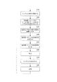
図1は、本発明の一実施形態に係る方法を用いるインプリント装置の構成を示す概略図である。ここでは、光硬化法を用いたインプリント装置として、紫外線の照射によって基板上の未硬化のインプリント材を硬化させる紫外線硬化型インプリント装置を使用した。ただし、インプリント材の硬化方法として、他の波長域の光の照射による方法や、他のエネルギー(例えば、熱)による方法を用いてもよい。また、以下の図においては、基板上のインプリント材に対して照射される紫外線の光軸に平行にZ軸を取り、Z軸に垂直な平面内に互いに直交するX軸およびY軸を取っている。本実施形態のインプリント装置は、インプリント処理を繰り返すことによって基板の複数のショット領域にパターンを形成するように構成されている。ここで、インプリント処理は、基板へのインプリント材の供給、型とインプリント材との接触および型のパターンへのインプリント材の充填、位置合わせ(アライメント)、硬化(露光)、型の剥離(離型)を含む、一連のサイクルのことを指すものとする。
(First Embodiment)
FIG. 1 is a schematic view showing the configuration of an imprinting apparatus using the method according to the embodiment of the present invention. Here, as an imprint device using the photocuring method, an ultraviolet curable imprint device that cures an uncured imprint material on a substrate by irradiation with ultraviolet rays was used. However, as a method for curing the imprint material, a method by irradiating light in another wavelength range or a method using other energy (for example, heat) may be used. Further, in the following figure, the Z-axis is taken parallel to the optical axis of the ultraviolet rays radiated to the imprint material on the substrate, and the X-axis and the Y-axis that are orthogonal to each other are taken in a plane perpendicular to the Z-axis. ing. The imprinting apparatus of this embodiment is configured to form a pattern in a plurality of shot regions of a substrate by repeating an imprinting process. Here, the imprinting process includes supplying the imprint material to the substrate, contacting the mold with the imprint material, filling the pattern of the mold with the imprint material, aligning (alignment), curing (exposure), and molding. It shall refer to a series of cycles including peeling (release).
インプリント装置100は、型保持機構110と、照射部120と、基板保持機構130と、ディスペンサ140と、アライメント計測部150と、距離計測部160と、制御部170と、を含む。
The
型保持機構110は、型(マスク、モールド)Mを保持するモールド保持部(型保持部)111と、モールドステージ(駆動機構)112と、モールド変形部(型変形部)113と、を含む。モールド保持部111による型Mの保持は、真空吸引力や静電気力等による。モールドステージ112は、モールド保持部111を機械的に保持する。モールドステージ112は、型Mの位置を6軸に関して制御したり、型Mを基板W、あるいは基板Wの上のインプリント材Rに押し付けたり、硬化したインプリント材Rから型Mを剥離(離型)したりする。ここで、6軸は、XYZ座標系におけるX軸、Y軸、Z軸およびそれらの各軸回りの回転である。モールドステージ112は、粗動駆動系および微動駆動系等といった複数の駆動系から構成されていても良い。モールド変形部113は、例えば、空気や油等の流体で作動するシリンダを用いて型Mを外周方向から加圧することによって型Mの形状を変形させることができる。その他、型Mの温度を制御することによって型Mの形状を変形させても良い。モールド変形部113は、基板Wの変形に応じて、基板Wと型Mとの重ね合わせ精度を向上させるように型Mの形状を補正する。
The
ここで、型Mは、例えば、外周部が矩形であり、基板Wに対向する面において、所定の凹凸パターンが3次元状に形成されており、紫外線を透過する材料(石英など)で構成される。基板Wは、凹凸パターンが転写される基板であって、例えば、単結晶シリコン基板やSOI(Silicon on Insulator)基板などを含む。 Here, in the mold M, for example, the outer peripheral portion is rectangular, a predetermined uneven pattern is formed in a three-dimensional shape on the surface facing the substrate W, and the mold M is made of a material (quartz or the like) that transmits ultraviolet rays. To. The substrate W is a substrate on which an uneven pattern is transferred, and includes, for example, a single crystal silicon substrate, an SOI (Silicon on Insulator) substrate, and the like.
照射部120は、光源121と、光学系122と、を含み、型Mを介してインプリント材Rに紫外光を照射して硬化させる。光源121は、例えば、紫外光(例えば、i線、g線)を発生する水銀ランプなどの光源と、該光源が発生した光を集光する楕円鏡とを含む。光学系122は、インプリント材Rを硬化させるための光を、基板W上のパターン形成領域(ショット領域)内のインプリント材に照射するためのレンズ、アパーチャ、ハーフミラーなどを含む。アパーチャは、画角制御や外周遮光制御に使用される。画角制御によって目標とするショット領域のみを照明することができ、外周遮光制御によって紫外光が基板Wのショット領域を超えて照射されることを制限することができる。光学系122は、型Mを均一に照明するためにオプティカルインテグレータを含んでもよい。アパーチャによって範囲が規定された光は、結像系(不図示)と型Mを介して基板W上のインプリント材Rに入射する。なお、熱硬化式のインプリント材Rを用いる場合、照射部120ではなくインプリント材Rを硬化させる為の熱源ユニットが必要となる。さらに、照射部120は、光源121とは別に、照射した光(加熱光)で基板Wを加熱して変形させるための基板加熱用光源(基板変形部)123を備えている。加熱光は、インプリント材Rが感光しない波長領域の光であり、かつアライメント計測部150が出射する計測光の波長と異なる波長領域の光である。加熱光としては、例えば、可視光を用いうる。
The
基板保持機構130は、基板保持部131と、基板ステージ(駆動機構)132と、を含む。基板保持部131は、基板Wの裏面を、例えば、機械的に保持する。基板ステージ132は、基板保持部131を機械的に保持する。基板ステージ132は、基板Wと型Mの位置合わせをするためのX軸方向及びY軸方向に駆動する駆動系である。また、X軸方向とY軸方向の駆動系は、粗動駆動系と微動駆動系等複数の駆動系から構成されていてもよい。さらに、Z軸方向の位置調整の為の駆動系や、基板Wのθ(Z軸周りの回転)方向の位置を調整する機能、基板Wの傾きを補正するためのチルト機能を有していても良い。
The
ディスペンサ140は、例えば、インプリント材Rを収容するタンクと、該タンクから供給路を通して供給されるインプリント材Rを基板Wに対して吐出するノズルと、該供給路に設けられたバルブと、供給量制御部とを有しうる。供給量制御部は、典型的には、1回のインプリント材Rの吐出動作において1つのショット領域にインプリント材Rが塗布されるように、バルブを制御することによって基板Wへのインプリント材Rの供給量を制御する。インプリント材Rの供給量は、必要となるインプリント材Rの厚さや転写するパターン密度等によって決定されうる。なお、供給量制御部は、制御部170で代用しても良い。
The
アライメント計測部150は、スコープ151と、スコープ161の光路を調整するハーフミラー152と、計測光を出射する光源(不図示)と、を含む。スコープ151は、型Mに形成されているモールド側マークと、基板Wに形成されている基板側マークとを型Mを介して検出する。本実施形態では、ダイバイダイ方式により、型Mと基板W(インプリント材R)とを近づけた状態で、モールド側マークおよび基板側マークを検出し、検出結果に基づいて型Mと基板Wとの位置合わせ(アライメント)を行う。
The
モールド側マークおよび基板側マークは、回折格子であり、アライメント計測部150は、各マークに計測光を照射して、各マークからの回折光を受光することで位置情報を検出する。各マークは、モールド側パターンおよび基板側パターンのそれぞれに複数設けられており、各マークの相対的な位置情報からモールド側パターンと基板側パターンとの相対位置や形状差を計測することができる。アライメント計測部150がnmオーダーで位置情報を検出するためには、モールド側マークと基板側マークとをできるだけ近づけることが望ましく、具体的には10μm以下の距離まで近づけることが望ましい。
The mold side mark and the substrate side mark are diffraction gratings, and the
距離計測部160は、型Mと基板W上のインプリント材Rとを接触させる接触位置において、型Mのモールド側パターン面の距離と傾きを計測する。距離計測部160は、例えば、基板ステージ132に設けられるとともに、モールド側パターン面に光(レーザ光)を照射するレーザ干渉計を含む。距離計測部160は、光が照射されたモールド側パターン面の箇所についての高さ(Z方向における位置)を検出するように構成されうる。そして、制御部170は、ベース定盤182に沿って基板ステージ132を移動させて、型Mのパターン面における複数の箇所の各々についての高さを距離計測部160に検出させる。これにより、距離計測部160は、型Mのモールド側パターン面における複数の箇所の各々について検出した高さにより、モールド側パターン面の傾きを計測する。同様に、型保持機構110にレーザ干渉計を配置して基板Wの基板側パターン面の、型保持機構110に対する距離と傾きを計測する。上記の計測結果から、モールドステージ112を駆動させて、型Mの傾きとZ位置を調整し、基板Wと型Mとの間の距離と平行度を制御している。基板保持機構130と型保持機構110は、インプリント装置100の組み立て及び調整時に絶対位置を保障している。距離計測部160による計測結果を用いて、インプリント装置100内に搬送される過程で発生する基板Wと型Mの受け渡し誤差を補正することもできる。
The
制御部170は、インプリント装置100の各構成要素(モールドステージ112等)の動作、及び調整処理等を制御する。制御部170は、インプリント装置の各構成要素に回線により接続された、磁気記憶媒体等の記憶手段を有するコンピュータ、又はシーケンサ等(不図示)で構成される。本実施形態に係る方法は、プログラムとしてコンピュータに実行されうる。その他に、インプリント装置100は、型Mを型保持機構110へ搬送するモールド搬送機構(不図示)、基板Wを基板保持機構130へ搬送する基板搬送機構(不図示)を有する。さらに、インプリント装置100は、型保持機構110を保持するブリッジ定盤180、ブリッジ定盤180を支える支柱181および、基板保持機構130を保持するベース定盤182を有する。
The
また、型保持機構110は、型Mの裏面(モールド側パターンが形成されている面と対向する面)に接する側にキャビティ(凹部)114を有しても良い。さらに、型保持機構110は、型保持機構110とキャビティ114とで囲まれる空間の圧力を制御する圧力調整部を有しうる。例えば、圧力を外部よりも高くしてモールド側パターンが−Z方向に撓んだ状態で型Mを基板Wに押し付けると、型Mは基板W上のインプリント材Rにモールド側パターンの中心部から接することになる。その結果、インプリント材Rと型Mとの間に空気が閉じ込められるのを抑制し、インプリント材の未充填欠陥を減らすことができる。
Further, the
図2は、インプリント材Rが供給された基板Wと型Mとの位置関係を示す図である。型Mには、上述したモールド側マークAM1と凹凸パターン(モールド側パターン)PMとが設けられている。基板Wには、上述した基板側マークAM2と基板側パターンPWとが設けられている。基板W上には、インプリント材Rが供給されている。型M(モールド側パターンPM)と基板W(基板側パターンPW)との距離を距離Dとする。本実施形態では、基板Wを変形させる際の距離Dを、インプリント材Rがモールド側パターンPMと接する接触距離d1より大きく、アライメント計測部150がモールド側マークAM1および基板側マークAM2を計測可能な距離d2以下とする。
FIG. 2 is a diagram showing a positional relationship between the substrate W to which the imprint material R is supplied and the mold M. The mold M, the mold-side mark AM1 described above and the concavo-convex pattern (mold-side pattern) P M is provided. The substrate W is provided with the substrate-side mark AM2 and the substrate-side pattern P W described above. The imprint material R is supplied on the substrate W. The distance between the mold M (the mold-side pattern P M) and the substrate W (the substrate-side pattern P W) and the distance D. In the present embodiment, the distance D when deforming the the substrate W, larger than the contact distance d 1 of imprint material R is in contact with the mold-side pattern P M,
距離Dが接触距離d1以下となる場合、すなわち、基板W上(=基板側パターン上)に供給されたインプリント材Rが型Mと接触する場合、型Mおよび基板Wに、型Mとインプリント材Rとの接触面に平行な方向の力(せん断力)が発生する可能性がある。例えば、型Mと基板Wとの間に挟まれたインプリント材Rの厚さがある値よりも薄くなると、インプリント材Rは、その成分中の分子の構造化によって高い粘弾性を示す。インプリント材Rの構造化は、含有成分の分子サイズや分子構造によって異なるが、一般的には、100nm以下の厚さで発生しうる。 When the distance D is less than or equal to the contact distance d 1 , that is, when the imprint material R supplied on the substrate W (= on the substrate side pattern ) comes into contact with the mold M, the mold M and the substrate W are combined with the mold M. A force (shearing force) in a direction parallel to the contact surface with the imprint material R may be generated. For example, when the thickness of the imprint material R sandwiched between the mold M and the substrate W becomes thinner than a certain value, the imprint material R exhibits high viscoelasticity due to the structuring of the molecules in the component. The structure of the imprint material R varies depending on the molecular size and molecular structure of the contained components, but generally can occur at a thickness of 100 nm or less.
インプリント材Rが構造化すると、例えば、基板加熱用光源123から出射した光で基板Wを熱変形させる際、インプリント材Rの高い粘弾性により、基板Wを所望の形状に変形させることが困難となりうる。そこで、本実施形態では、基板Wを熱変形させる際の距離Dを、接触距離d1より大きく、距離d2以下とする。これにより、インプリント材Rの構造化による影響を受けずに型Mと基板Wとの重ね合わせ精度を向上させることができる。
When the imprint material R is structured, for example, when the substrate W is thermally deformed by the light emitted from the substrate
図3は、第1実施形態に係るインプリント方法を示すフローチャートである。工程S10でディスペンサ140は、基板W上(=基板側パターンPW上)にインプリント材Rを供給する。工程S20で制御部170は、基板ステージ132を駆動して基板側パターンPWとモールド側パターンPMとのXY方向の位置を合わせる。工程S30で制御部170は、モールドステージ112を駆動して、基板Wと型Mとの距離Dが、d1<D≦d2となるように型Mを−Z方向に移動させる。接触距離d1は、インプリント材Rがモールド側パターンPMと接する距離であり、基板側パターンPWとモールド側パターンPMとの間がインプリント材Rで完全に充填される距離である。
FIG. 3 is a flowchart showing an imprint method according to the first embodiment. In step S10, the
工程S40で制御部170は、アライメント計測部150を制御して基板側パターンPWとモールド側パターンPMとの形状差、相対位置を計測する。工程S50で制御部170は、工程S40で得た計測結果から、基板側パターンPWの補正量を算出し、基板側パターンPWを当該補正量分変形させる温度分布を求める。制御部170は、基板加熱用光源123を制御して、基板W上に求めた温度分布を形成する。工程S40および工程S50において、基板Wと型Mとの距離Dは、工程S30で設定された距離が維持されている。本実施形態では、基板Wと型Mとの距離Dが、d1<D≦d2の条件を充たしているためインプリント材Rが構造化することなく基板側パターンPWを所望の形状に熱変形させることができる。
工程S50により基板側パターンPWとモールド側パターンPMとの形状を合わせた後、工程S60に進む。工程S60で制御部170は、モールドステージ112または基板ステージ132を制御して型Mを基板W上のインプリント材Rに押し付けて(距離Dを距離d2へ変化させる)、モールド側パターンPMにインプリント材を充填する(押型)。工程S70で制御部170は、照射部120を制御してインプリント材Rに紫外線を照射して硬化させる。インプリント材Rが硬化したら、工程S80で制御部170は、モールドステージ112または基板ステージ132を制御して型Mを基板W上のインプリント材Rから剥がす(離型)。続いて、つぎのショットのインプリント処理に移るため、工程S10に戻り、工程S20〜工程S80を繰り返す。以上の工程により、基板W上に硬化したインプリント材Rの凹凸パターンが形成される。
After combining the shape of the substrate-side pattern P W and the mold-side pattern P M by step S50, the process proceeds to step S60. In step S60, the
以上のように、基板側パターンPWおよびモールド側パターンPMの形状を計測でき、かつモールド側パターンPMにインプリント材Rが接触しない範囲で基板Wと型Mとを近づけることでインプリント材Rの構造化の影響を抑えることができる。したがって、インプリント材Rの厚みによらず基板側パターンPWを変形させてモールド側パターンPMの形状と合わせることができる。本実施形態によれば、基板と型との重ね合わせ精度の向上に有利なインプリント装置を提供することができる。 As described above, the substrate-side pattern P W and can measure the shape of the mold-side pattern P M, and imprinted by close the substrate W and the mold M to the extent that the imprint material R is not in contact with the mold-side pattern P M The influence of the structuring of the material R can be suppressed. Therefore, it is possible to match by deforming the substrate side pattern P W regardless of the thickness of the imprint material R to the shape of the mold-side pattern P M. According to this embodiment, it is possible to provide an imprinting apparatus which is advantageous for improving the superposition accuracy of the substrate and the mold.
基板Wと型Mとの温度差があると、押型する際に、例えば、型Mから基板Wへ熱が伝わり基板側パターンPWの形状が所望の形状から変形してしまう場合がある。そこで、本実施形態では、基板Wの温度と型Mの温度との差を考慮して上記工程S60を行う。図4は、基板Wと型Mとの温度差の時間変化を示すグラフである。上記工程S50により基板Wの加熱を開始してからの時間を横軸、基板Wまたは型Mの温度を縦軸としている。実線は基板Wの温度T0の変化曲線、点線は型Mと基板Wとの距離を所定の距離にした場合の型Mの温度T 2 の変化曲線、2点鎖線は、型Mと基板Wとが所定の距離よりも離れている場合の型Mの温度T 1 の変化曲線とする。 If there is a temperature difference between the substrate W and the mold M, heat may be transferred from the mold M to the substrate W when the mold is pressed, and the shape of the substrate side pattern PW may be deformed from a desired shape. Therefore, in the present embodiment, the above step S60 is performed in consideration of the difference between the temperature of the substrate W and the temperature of the mold M. FIG. 4 is a graph showing the time change of the temperature difference between the substrate W and the mold M. The time from the start of heating the substrate W in the above step S50 is on the horizontal axis, and the temperature of the substrate W or mold M is on the vertical axis. Change curve temperature T0 of the solid substrate W, the change curve of the temperature T 2 of the mold M when the dotted line is where the distance between the mold M and the substrate W to a predetermined distance, two-dot chain line, the mold M and the substrate W Let be the change curve of the temperature T 1 of the type M when is more than a predetermined distance.
所定の距離は、基板側パターンPWの形状補正が完了した時点で基板Wと型Mとの温度差が許容値となるように決定される。温度差の許容値は、基板Wの線膨張係数、所望の変形誤差等により決定される。例えば、基板側パターンPWおよびモールド側パターンPMのサイズを33mm×26mmとし、基板側パターンPW(基板W)の材質Siの線膨張係数を2.62×10⁻⁶[1/K]とする。基板側パターンPWの温度が0.01℃変化すると、33[mm]×2.62×10−6[1/K]×0.01[K]=0.86[nm]でおよそ1nm変形する。変形誤差を1nm以下に抑えたい場合は、温度差を0.01℃以下とすることが望ましい。 The predetermined distance is determined so that the temperature difference between the substrate W and the mold M becomes an allowable value when the shape correction of the substrate side pattern P W is completed. The permissible value of the temperature difference is determined by the linear expansion coefficient of the substrate W, the desired deformation error, and the like. For example, the size of the substrate-side pattern P W and the mold-side pattern P M and 33 mm × 26 mm, the substrate-side pattern P W (substrate W) Material Si linear expansion coefficient of the 2.62 × 10 -6 [1 / K ] of the And. When the temperature of the substrate side pattern P W changes by 0.01 ° C, it is deformed by about 1 nm at 33 [mm] × 2.62 × 10⁻⁶ [1 / K] × 0.01 [K] = 0.86 [nm]. To do. When it is desired to suppress the deformation error to 1 nm or less, it is desirable to set the temperature difference to 0.01 ° C. or less.
基板Wと型Mとの温度差は時間経過とともに小さくなってゆくが、図4の曲線T1と曲線T2とを比較すると、基板Wと型Mとの温度差が許容値になるまでの時間が曲線T2の方が早い。これは、基板Wと型Mとを近づけることで、基板Wと型Mとの間の空気を介した熱抵抗が減少するためである。本実施形態では、温度差が許容値となってから工程S60の押型を行う。曲線T 2 の場合では、基板側パターンPWの形状補正が完了した時点で温度差が許容値となっており、すみやかに工程S60を行うことができる。一方、曲線T 1 の場合では、温度差が許容値となるまでの待機時間が必要となる。つまり、基板Wと型Mとの距離Dを、d1<D≦d2を充たし、かつ、基板側パターンPWの形状補正が完了した時点で基板Wと型Mとの温度差が許容値となるように決定することでスループットを向上させることができる。 The temperature difference between the substrate W and the mold M becomes smaller with the passage of time, but when comparing the curves T1 and T2 in FIG. 4, it takes time for the temperature difference between the substrate W and the mold M to reach an allowable value. The curve T2 is faster. This is because the thermal resistance between the substrate W and the mold M via air is reduced by bringing the substrate W and the mold M closer to each other. In the present embodiment, the stamping in step S60 is performed after the temperature difference becomes an allowable value. In the case of the curve T 2 , the temperature difference becomes an allowable value when the shape correction of the substrate side pattern PW is completed, and the step S60 can be performed promptly. On the other hand, in the case of the curve T 1 , a waiting time is required until the temperature difference becomes an allowable value. That is, the distance D between the substrate W and the mold M is such that the temperature difference between the substrate W and the mold M becomes an allowable value when d1 <D ≦ d2 is satisfied and the shape correction of the substrate side pattern PW is completed. Throughput can be improved by deciding to.
図5は、型Mの温度および基板Wの温度を計測する温度センサの配置を示す図である。モールド側パターンPMの温度は、型Mのモールド側パターンPMが形成された面の反対側の面に配置された温度センサ200により計測される。温度センサ200は、型Mの露光領域と干渉しないように、モールド側パターンPMが形成された面の反対側の面の周囲に配置するのが望ましい。温度センサ200として用いるのは、例えば、熱電対、サーミスタ、白金測温抵抗体、等がありうる。
FIG. 5 is a diagram showing an arrangement of temperature sensors that measure the temperature of the mold M and the temperature of the substrate W. Temperature of the mold-side pattern P M is measured by the
基板保持部131は、例えば、チャックピン133をさらに備える。基板側パターンPWの温度は、温度センサ201をチャックピン133に配置して、基板Wを保持する際に基板Wの裏面に接触させることで計測される。または、隣り合うチャックピン133の間の溝に温度センサ202を配置し、溝の空間の熱伝導率を考慮して計測を行ってもよい。温度センサ201および202として用いるのは、上記と同様に、例えば、熱電対、サーミスタ、白金測温抵抗体、等がありうる。基板Wと型Mとの温度差は、温度センサ200〜202の出力に基づいて求めることができる。
The
基板Wと型Mとの温度差をより速やかに小さくするために、型Mの周囲に不図示の気体供給部を設けてもよい。気体供給部は、工程S50(基板Wの加熱)から工程S60(押型)までの間、基板Wと型Mとの間を、空気より熱伝導率[W/m・K]が高い気体(He等)で置換する。基板Wと型Mとの間を熱伝導率が高い気体で満たすことで、基板Wと型Mとの温度差をより迅速に許容値以下にすることができる。 In order to reduce the temperature difference between the substrate W and the mold M more quickly, a gas supply unit (not shown) may be provided around the mold M. The gas supply unit is a gas (He) having a higher thermal conductivity [W / m · K] than air between the substrate W and the mold M from the step S50 (heating of the substrate W) to the step S60 (stamping). Etc.). By filling the space between the substrate W and the mold M with a gas having a high thermal conductivity, the temperature difference between the substrate W and the mold M can be made less than the permissible value more quickly.
また、工程S50にて基板Wを加熱する際、型Mも同時に加熱されうる。しかし、型Mの材質である石英の熱膨張係数は基板Wの材質であるシリコン等と比べて十分小さいため、モールド側パターンPMの熱変形は基板側パターンPWの補正量に対してごくわずかである。さらに、モールド側パターンPMの熱変形分は、型変形部113により補正することもできる。本実施形態によって、押型時の基板側パターンPWの不要な温度変化を抑え、より精度の高いパターン形状補正を行うことができる。
Further, when the substrate W is heated in step S50, the mold M can also be heated at the same time. However, since the thermal expansion coefficient of quartz is a material of the type M is sufficiently smaller than the silicon, which is the material of the substrate W, the thermal deformation of the mold-side pattern P M is small with respect to the correction amount of the substrate-side pattern P W There are few. Furthermore, the thermal deformation amount of the mold-side pattern P M can be corrected by the
以上の実施形態はその限りではなく、それぞれを組み合わせても構わない。なお、上記実施形態では、ショット毎に基板側パターンPWの形状を計測しているが、例えば、全てのショットの基板側パターンPWの形状を計測しておいて、2回目のフローでは、工程S40を省略してもよい。また、基板側パターンPWの形状の計測は、工程S10のインプリント材Rの供給前に行ってもよい。すなわち、基板Wが基板保持機構130に搬送された後に行ってもよいし、インプリント装置100内にある別の計測エリアで事前に行われてもよい。また、インプリント装置100に基板Wを搬入する前に予め不図示の基板計測装置で行われていてもよい。また、型Mと基板Wとの温度差は、上記温度センサを用いずに、距離計測部160の計測結果から、型Mと基板Wとの間の距離に基づいて、型Mと基板Wとの間の空間の熱伝導率から求めることもできる。さらに、インプリント装置100の組み立て及び調整時に設定された、型M(モールド保持部111)と基板W(基板保持部131)との間の距離に基づいて、型Mと基板Wとの間の空間の熱伝導率から温度差を求めることもできる。型Mと基板Wとの温度差は、温度センサ、距離計測部および組み立て及び調整時に設定された型Mと基板Wとの間の距離のいずれか1つ以上を組み合わせて求めても良い。
The above embodiments are not limited to this, and each may be combined. In the above embodiment, the shape of the substrate side pattern P W is measured for each shot. For example, the shape of the substrate side pattern P W of all shots is measured, and in the second flow, the shape is measured. Step S40 may be omitted. Further, the shape of the substrate-side pattern P W may be measured before the imprint material R in step S10 is supplied. That is, it may be performed after the substrate W has been conveyed to the
(物品製造方法に係る実施形態)
物品としてのデバイス(半導体集積回路素子、液晶表示素子等)の製造方法は、上述した型を用いたインプリント装置を用いて基板(ウエハ、ガラスプレート、フィルム状基板)上にインプリント材のパターンを形成する工程を含む。さらに、該製造方法は、パターンを形成された基板をエッチングする工程を含みうる。なお、パターンドメディア(記録媒体)や光学素子などの他の物品を製造する場合には、該製造方法は、エッチングの代わりにパターンを形成された基板を加工する他の処理を含みうる。本実施形態の物品の製造方法は、従来の方法に比べて、物品の性能・品質・生産性・生産コストの少なくとも1つにおいて有利である。
(Embodiment relating to article manufacturing method)
A method for manufacturing a device as an article (semiconductor integrated circuit element, liquid crystal display element, etc.) is a pattern of an imprint material on a substrate (wafer, glass plate, film-like substrate) using an imprint device using the above-mentioned mold. Includes the step of forming. Further, the manufacturing method may include a step of etching the patterned substrate. When manufacturing other articles such as patterned media (recording media) and optical elements, the manufacturing method may include other processing of processing a patterned substrate instead of etching. The method for producing an article of the present embodiment is advantageous in at least one of the performance, quality, productivity, and production cost of the article as compared with the conventional method.
(その他の実施形態)
以上、本発明の実施の形態を説明してきたが、本発明はこれらの実施の形態に限定されず、その要旨の範囲内において様々な変更が可能である。
(Other embodiments)
Although the embodiments of the present invention have been described above, the present invention is not limited to these embodiments, and various modifications can be made within the scope of the gist thereof.
100 インプリント装置
150 アライメント計測部
123 基板加熱用光源(基板変形部)
M 型
W 基板
PM 型側パターン
PW 基板側パターン
R インプリント材
100
M type W substrate P M-type-side pattern P W substrate-side pattern R imprint material
Claims (12)
前記型側パターンと前記基板側パターンとの形状差に関する情報を得る計測部と、
前記基板側パターンを加熱して変形させる加熱変形部と、
前記型側パターンと前記インプリント材とが接触するように前記型と前記基板との距離を調整する駆動機構と、
前記計測部と前記加熱変形部と前記駆動機構とを制御する制御部と、を有し、
前記制御部は、前記駆動機構によって前記距離を、前記型側パターンが前記インプリント材と接触する接触距離よりも長い第1距離に調整した状態で、前記計測部で前記形状差に関する前記情報を取得し、
前記駆動機構によって前記距離を前記第1距離に調整した状態で、前記計測部が得た前記情報に基づいて、前記形状差を少なくするように前記加熱変形部でパターンを変形させ、
前記基板側パターンの変形が完了している状態、かつ、前記型側パターンと前記基板側パターンとの間の温度差が所定の値以下となるように前記型側パターンの温度が上昇した時点で、前記駆動機構により前記距離が前記第1距離から前記接触距離に調整される、ように制御し、
さらに、前記制御部は、前記温度差を、予め設定された前記型側パターンと前記基板側パターンとの位置関係に基づいて得られた前記距離から求めることを特徴とするインプリント装置。 An imprinting apparatus that forms an imprint material pattern on the substrate by bringing the mold-side pattern formed on the mold and the uncured imprint material supplied on the substrate-side pattern formed on the substrate into contact with each other. And
A measuring unit for obtaining information about the shape Josashi between the substrate-side pattern and the mold-side pattern,
A heat-deformed portion that heats and deforms the substrate-side pattern,
A drive mechanism that adjusts the distance between the mold and the substrate so that the mold-side pattern and the imprint material come into contact with each other.
It has a measuring unit, a heating deformation unit, and a control unit that controls the driving mechanism .
Wherein the control unit, the distance by the drive mechanism, in a state where the mold-side pattern is adjusted to the long first distance than the contact distance in contact with the imprint material, wherein for the previous SL form Josashi by the measuring unit to get the information,
Wherein while adjusting the distance to the first distance by the drive mechanism, on the basis of the information which the measuring unit is obtained, to deform the front Symbol pattern in the heat deformation portion to the reduced form Josashi,
State deformation before Symbol substrate-side pattern has been completed and, when the temperature difference between the mold-side pattern and the substrate-side patterns temperature of the mold-side pattern to be equal to or less than a predetermined value is increased in the distance by the drive mechanism is adjusted to the contact distance from the first distance, and controls so that,
Further, the control unit is an imprinting apparatus characterized in that the temperature difference is obtained from the distance obtained based on the positional relationship between the mold side pattern and the substrate side pattern set in advance.
前記型側パターンと前記基板側パターンとの形状差に関する情報を得る計測部と、A measuring unit that obtains information on the shape difference between the mold-side pattern and the substrate-side pattern,
前記基板側パターンを加熱して変形させる加熱変形部と、A heat-deformed portion that heats and deforms the substrate-side pattern,
前記型側パターンと前記インプリント材とが接触するように前記型と前記基板との距離を調整する駆動機構と、A drive mechanism that adjusts the distance between the mold and the substrate so that the mold-side pattern and the imprint material come into contact with each other.
前記計測部と前記加熱変形部と前記駆動機構とを制御する制御部と、を有し、It has a measuring unit, a heating deformation unit, and a control unit that controls the driving mechanism.
前記制御部は、前記駆動機構によって前記距離を、前記型側パターンが前記インプリント材と接触する接触距離よりも長い第1距離に調整した状態で、前記計測部で前記形状差に関する前記情報を取得し、The control unit adjusts the distance to a first distance longer than the contact distance at which the mold-side pattern contacts the imprint material by the drive mechanism, and the measuring unit obtains the information regarding the shape difference. Acquired,
前記駆動機構によって前記距離を前記第1距離に調整した状態で、前記計測部が得た前記情報に基づいて、前記形状差を少なくするように前記加熱変形部でパターンを変形させ、In a state where the distance is adjusted to the first distance by the drive mechanism, the pattern is deformed by the heating deformation unit so as to reduce the shape difference based on the information obtained by the measurement unit.
前記基板側パターンの変形が完了している状態、かつ、前記型側パターンと前記基板側パターンとの間の温度差が所定の値以下となるように前記型側パターンの温度が上昇した時点で、前記駆動機構により前記距離が前記第1距離から前記接触距離に調整される、ように制御し、When the deformation of the substrate-side pattern is completed and the temperature of the mold-side pattern rises so that the temperature difference between the mold-side pattern and the substrate-side pattern becomes equal to or less than a predetermined value. The drive mechanism controls the distance so that the distance is adjusted from the first distance to the contact distance.
当該インプリント装置は、前記距離を計測する距離計測部をさらに有し、The imprint device further includes a distance measuring unit for measuring the distance.
前記制御部は、前記温度差を、前記距離計測部による前記距離の計測結果に基づいて求めることを特徴とするインプリント装置。The control unit is an imprint device that obtains the temperature difference based on the measurement result of the distance by the distance measuring unit.
前記制御部は、前記形状差を少なくするように前記型変形部も制御する
ことを特徴とする請求項1または2に記載のインプリント装置。 Further comprising a mold deformation part for deforming the front SL type-side pattern,
The imprint device according to claim 1 or 2 , wherein the control unit also controls the mold deformation unit so as to reduce the shape difference.
前記型側パターンと前記基板側パターンとの形状差に関する情報を得る計測部と、
前記基板側パターンを加熱して変形させる加熱変形部と、
前記型側パターンを変形させる型変形部と、
前記型側パターンと前記インプリント材とが接触するように前記型と前記基板との距離を調整する駆動機構と、
前記計測部と前記加熱変形部と前記駆動機構とを制御する制御部と、を有し、
前記制御部は、前記駆動機構によって前記距離を、前記型側パターンが前記インプリント材と接触する接触距離よりも長い第1距離に調整した状態で、前記計測部は前記形状差に関する前記情報を取得し、
前記計測部が得た前記情報に基づいて、前記形状差を少なくするように、前記加熱変形部および前記型変形部の少なくとも一方はパターンを変形させ、
前記パターンの変形が完了している状態、かつ、前記型側パターンと前記基板側パターンとの間の温度差が所定の値以下となるように前記型側パターンの温度が上昇した時点で、前記駆動機構により前記距離が前記接触距離に調整される、ように制御し、
さらに、前記制御部は、前記温度差を、予め設定された前記型側パターンと前記基板側パターンとの位置関係に基づいて得られた前記距離から求めることを特徴とするインプリント装置。 An imprinting apparatus that forms an imprint material pattern on the substrate by bringing the mold-side pattern formed on the mold and the uncured imprint material supplied on the substrate-side pattern formed on the substrate into contact with each other. And
A measuring unit for obtaining information about the shape Josashi between the substrate-side pattern and the mold-side pattern,
A heat-deformed portion that heats and deforms the substrate-side pattern,
A mold deforming part that deforms the mold side pattern and
A drive mechanism that adjusts the distance between the mold and the substrate so that the mold-side pattern and the imprint material come into contact with each other.
It has a measuring unit, a heating deformation unit, and a control unit that controls the driving mechanism .
Wherein the control unit, the distance by the drive mechanism, in a state where the mold-side pattern is adjusted to the long first distance than the contact distance in contact with the imprint material, the measuring unit the related prior Symbol form Josashi to get the information,
The measurement unit based on the information obtained so as to reduce the pre-Symbol form Josashi, at least one of the heat deformation portion and the shape modification section deforms the pattern,
State deformation of the pattern is complete, and in that when the temperature difference between the mold-side pattern and the substrate-side patterns temperature of the mold-side pattern to be equal to or less than a predetermined value is increased , said distance by said driving mechanism is adjusted to the contact distance, controls as,
Further, the control unit is an imprinting apparatus characterized in that the temperature difference is obtained from the distance obtained based on the positional relationship between the mold side pattern and the substrate side pattern set in advance.
前記型側パターンと前記基板側パターンとの形状差に関する情報を得る計測部と、A measuring unit that obtains information on the shape difference between the mold-side pattern and the substrate-side pattern,
前記基板側パターンを加熱して変形させる加熱変形部と、A heat-deformed portion that heats and deforms the substrate-side pattern,
前記型側パターンを変形させる型変形部と、A mold deforming part that deforms the mold side pattern and
前記型側パターンと前記インプリント材とが接触するように前記型と前記基板との距離を調整する駆動機構と、A drive mechanism that adjusts the distance between the mold and the substrate so that the mold-side pattern and the imprint material come into contact with each other.
前記計測部と前記加熱変形部と前記駆動機構とを制御する制御部と、を有し、It has a measuring unit, a heating deformation unit, and a control unit that controls the driving mechanism.
前記制御部は、前記駆動機構によって前記距離を、前記型側パターンが前記インプリント材と接触する接触距離よりも長い第1距離に調整した状態で、前記計測部は前記形状差に関する前記情報を取得し、The control unit adjusts the distance by the drive mechanism to a first distance longer than the contact distance at which the mold-side pattern contacts the imprint material, and the measuring unit obtains the information regarding the shape difference. Acquired,
前記計測部が得た前記情報に基づいて、前記形状差を少なくするように、前記加熱変形部および前記型変形部の少なくとも一方はパターンを変形させ、Based on the information obtained by the measuring unit, at least one of the heat-deformed portion and the mold-deformed portion deforms the pattern so as to reduce the shape difference.
前記パターンの変形が完了している状態、かつ、前記型側パターンと前記基板側パターンとの間の温度差が所定の値以下となるように前記型側パターンの温度が上昇した時点で、前記駆動機構により前記距離が前記接触距離に調整される、ように制御し、When the deformation of the pattern is completed and the temperature of the mold-side pattern rises so that the temperature difference between the mold-side pattern and the substrate-side pattern becomes equal to or less than a predetermined value, the above-mentioned The drive mechanism controls the distance so that it is adjusted to the contact distance.
当該インプリント装置は、前記距離を計測する距離計測部をさらに有し、The imprint device further includes a distance measuring unit for measuring the distance.
前記制御部は、前記温度差を、前記距離計測部による前記距離の計測結果に基づいて求めることを特徴とするインプリント装置。The control unit is an imprint device that obtains the temperature difference based on the measurement result of the distance by the distance measuring unit.
前記型保持部は、前記型側パターンの温度を計測する第1センサを備え、
前記基板保持部は、前記基板側パターンの温度を計測する第2センサを備え、
前記温度差は、前記第1センサの出力および前記第2センサの出力に基づいて求められることを特徴とする請求項1ないし7のいずれか1項に記載のインプリント装置。 Further having a mold holding portion for holding the mold and a substrate holding portion for holding the substrate,
The mold holder includes a first sensor that measures the temperature of the mold side pattern.
The substrate holding portion includes a second sensor that measures the temperature of the substrate side pattern.
The imprint device according to any one of claims 1 to 7 , wherein the temperature difference is obtained based on the output of the first sensor and the output of the second sensor.
前記制御部は、前記駆動機構により前記第1距離に調整している状態おいて、前記パターンの変形が終わるまで前記気体が供給されるように、前記気体供給部を制御することを特徴とする請求項1ないし8のうちいずれか1項に記載のインプリント装置。 A gas supply unit that supplies a gas having a higher thermal conductivity than air is provided between the mold and the substrate.
Wherein the control unit, the state Oite are adjusted to the first distance by the drive mechanism, so that the gas to deformation of the pattern end of the Ru is supplied, and controls the gas supply unit The imprint device according to any one of claims 1 to 8.
前記制御部は、前記計測部で前記型側パターンおよび前記基板側パターンを当該第1光源からの第1の波長の光で計測して、前記形状差に関する情報を取得し、
前記加熱変形部は、前記基板側パターンを加熱する第2光源であって、前記第1の波長とは異なる第2の波長の光を出射する当該第2光源を備えることを特徴とする請求項1ないし8のうちいずれか1項に記載のインプリント装置。 The measuring unit includes a first light source that emits light having a first wavelength that illuminates the mold-side pattern and the substrate-side pattern.
Wherein the control unit, the said mold side pattern and the substrate-side patterns measuring unit measures with light of the first wavelength from the first light source, to obtain information about previous SL form Josashi,
The heating deformation portion is a second light source that heats the substrate side pattern, and includes the second light source that emits light having a second wavelength different from the first wavelength. The imprinting apparatus according to any one of 1 to 8.
前記型と前記基板との距離を、前記型側パターンが前記インプリント材と接触する接触距離よりも長い第1距離に調整し、
前記第1距離において、前記型側パターンと前記基板側パターンとの形状差に関する情報を得、
前記第1距離において、前記情報に基づいて、前記形状差を少なくするように前記基板側パターンを加熱により変形させ、
前記型側パターンと前記基板側パターンとの間の温度差であって、予め設定された前記型側パターンと前記基板側パターンとの位置関係に基づいて得られた前記距離から求められる当該温度差が所定の値以下となる時点で、前記距離を前記第1距離から前記接触距離に調整することを特徴とするインプリント方法。 An imprint method in which a mold-side pattern formed on a mold and an uncured imprint material supplied to the substrate-side pattern formed on a substrate are brought into contact with each other to form an imprint material pattern on the substrate. There,
The distance between the mold and the substrate is adjusted to a first distance longer than the contact distance at which the mold side pattern contacts the imprint material.
In the first distance, to obtain information about the shape Josashi of the mold-side pattern and the substrate-side pattern,
In the first distance, on the basis of the information, it is deformed by heating the substrate-side pattern so as to reduce the pre-Symbol form Josashi,
The temperature difference between the mold-side pattern and the substrate-side pattern, which is obtained from the distance obtained based on the preset positional relationship between the mold-side pattern and the substrate-side pattern. An imprint method comprising adjusting the distance from the first distance to the contact distance when is equal to or less than a predetermined value.
前記工程で前記パターンを形成された前記基板を加工する工程と、
を含むことを特徴とする物品製造方法。 A step of forming a pattern on a substrate by using the imprinting apparatus according to any one of claims 1 to 10 or the imprinting method according to claim 11.
A step of processing the substrate on which the pattern is formed in the step and a step of processing the substrate
A method for manufacturing an article, which comprises.
Priority Applications (1)
| Application Number | Priority Date | Filing Date | Title |
|---|---|---|---|
| JP2016207765A JP6866106B2 (en) | 2016-10-24 | 2016-10-24 | Imprinting equipment, imprinting methods, and manufacturing methods for goods |
Applications Claiming Priority (1)
| Application Number | Priority Date | Filing Date | Title |
|---|---|---|---|
| JP2016207765A JP6866106B2 (en) | 2016-10-24 | 2016-10-24 | Imprinting equipment, imprinting methods, and manufacturing methods for goods |
Publications (3)
| Publication Number | Publication Date |
|---|---|
| JP2018073862A JP2018073862A (en) | 2018-05-10 |
| JP2018073862A5 JP2018073862A5 (en) | 2019-11-28 |
| JP6866106B2 true JP6866106B2 (en) | 2021-04-28 |
Family
ID=62115719
Family Applications (1)
| Application Number | Title | Priority Date | Filing Date |
|---|---|---|---|
| JP2016207765A Active JP6866106B2 (en) | 2016-10-24 | 2016-10-24 | Imprinting equipment, imprinting methods, and manufacturing methods for goods |
Country Status (1)
| Country | Link |
|---|---|
| JP (1) | JP6866106B2 (en) |
Families Citing this family (1)
| Publication number | Priority date | Publication date | Assignee | Title |
|---|---|---|---|---|
| JP7278163B2 (en) * | 2019-07-11 | 2023-05-19 | キヤノン株式会社 | IMPRINT APPARATUS AND ARTICLE MANUFACTURING METHOD |
Family Cites Families (7)
| Publication number | Priority date | Publication date | Assignee | Title |
|---|---|---|---|---|
| JP2004259985A (en) * | 2003-02-26 | 2004-09-16 | Sony Corp | Resist pattern forming device, method for forming resist pattern and method for manufacturing semiconductor device using the forming method |
| JP4217551B2 (en) * | 2003-07-02 | 2009-02-04 | キヤノン株式会社 | Fine processing method and fine processing apparatus |
| JP5686779B2 (en) * | 2011-10-14 | 2015-03-18 | キヤノン株式会社 | Imprint apparatus and article manufacturing method using the same |
| JP2013125817A (en) * | 2011-12-14 | 2013-06-24 | Canon Inc | Imprint device, imprint method, and article manufacturing method using the device or the method |
| JP6180131B2 (en) * | 2012-03-19 | 2017-08-16 | キヤノン株式会社 | Imprint apparatus and article manufacturing method using the same |
| JP6329353B2 (en) * | 2013-10-01 | 2018-05-23 | キヤノン株式会社 | Imprint apparatus and article manufacturing method |
| JP2017188556A (en) * | 2016-04-05 | 2017-10-12 | キヤノン株式会社 | Imprint device, imprint method, method of manufacturing article, and mold |
-
2016
- 2016-10-24 JP JP2016207765A patent/JP6866106B2/en active Active
Also Published As
| Publication number | Publication date |
|---|---|
| JP2018073862A (en) | 2018-05-10 |
Similar Documents
| Publication | Publication Date | Title |
|---|---|---|
| US11249394B2 (en) | Imprint methods for forming a pattern of an imprint material on a substrate-side pattern region of a substrate by using a mold, and related device manufacturing methods | |
| JP6818859B2 (en) | Imprinting equipment, imprinting method and manufacturing method of goods | |
| TWI601619B (en) | Imprint apparatus and article manufacturing method | |
| JP6180131B2 (en) | Imprint apparatus and article manufacturing method using the same | |
| JP6362399B2 (en) | Imprint apparatus, imprint method, and article manufacturing method | |
| JP6333039B2 (en) | Imprint apparatus, device manufacturing method, and imprint method | |
| JP6418773B2 (en) | Imprint apparatus, imprint method, and article manufacturing method | |
| JP6029494B2 (en) | Imprint method, imprint apparatus, and article manufacturing method using the same | |
| TWI720301B (en) | Imprint apparatus and method of manufacturing article | |
| JP4963718B2 (en) | Imprint method, imprint apparatus, and article manufacturing method using the same | |
| JP6120677B2 (en) | Imprint apparatus, imprint method, and article manufacturing method | |
| US9927700B2 (en) | Imprint apparatus, and method of manufacturing article | |
| JP6552185B2 (en) | Imprint apparatus, correction mechanism calibration method, and article manufacturing method | |
| JP2013125817A (en) | Imprint device, imprint method, and article manufacturing method using the device or the method | |
| JP6590598B2 (en) | Imprint apparatus, imprint method, and article manufacturing method | |
| JP6866106B2 (en) | Imprinting equipment, imprinting methods, and manufacturing methods for goods | |
| JP7027037B2 (en) | Mold duplication method, imprinting device, and article manufacturing method | |
| JP5865528B2 (en) | Imprint apparatus, imprint method, and device manufacturing method | |
| JP7451141B2 (en) | Imprint device, imprint method, and article manufacturing method | |
| JP7179655B2 (en) | IMPRINT APPARATUS, IMPRINT METHOD, AND ARTICLE MANUFACTURING METHOD | |
| JP2017183364A (en) | Imprinting method, imprinting device, program, and manufacturing method for article | |
| JP6797627B2 (en) | Imprinting equipment, imprinting methods, and manufacturing methods for articles | |
| TW202226427A (en) | Substrate processing method, substrate holding apparatus, molding apparatus, and article manufacturing method |
Legal Events
| Date | Code | Title | Description |
|---|---|---|---|
| A521 | Written amendment |
Free format text: JAPANESE INTERMEDIATE CODE: A523 Effective date: 20191018 |
|
| A621 | Written request for application examination |
Free format text: JAPANESE INTERMEDIATE CODE: A621 Effective date: 20191018 |
|
| A977 | Report on retrieval |
Free format text: JAPANESE INTERMEDIATE CODE: A971007 Effective date: 20200928 |
|
| A131 | Notification of reasons for refusal |
Free format text: JAPANESE INTERMEDIATE CODE: A131 Effective date: 20201006 |
|
| A521 | Written amendment |
Free format text: JAPANESE INTERMEDIATE CODE: A523 Effective date: 20201204 |
|
| TRDD | Decision of grant or rejection written | ||
| A01 | Written decision to grant a patent or to grant a registration (utility model) |
Free format text: JAPANESE INTERMEDIATE CODE: A01 Effective date: 20210309 |
|
| A61 | First payment of annual fees (during grant procedure) |
Free format text: JAPANESE INTERMEDIATE CODE: A61 Effective date: 20210407 |
|
| R151 | Written notification of patent or utility model registration |
Ref document number: 6866106 Country of ref document: JP Free format text: JAPANESE INTERMEDIATE CODE: R151 |