JP6865202B2 - Communications system - Google Patents
Communications system Download PDFInfo
- Publication number
- JP6865202B2 JP6865202B2 JP2018196432A JP2018196432A JP6865202B2 JP 6865202 B2 JP6865202 B2 JP 6865202B2 JP 2018196432 A JP2018196432 A JP 2018196432A JP 2018196432 A JP2018196432 A JP 2018196432A JP 6865202 B2 JP6865202 B2 JP 6865202B2
- Authority
- JP
- Japan
- Prior art keywords
- master device
- block
- slave
- output
- power supply
- Prior art date
- Legal status (The legal status is an assumption and is not a legal conclusion. Google has not performed a legal analysis and makes no representation as to the accuracy of the status listed.)
- Active
Links
- 238000004891 communication Methods 0.000 title claims description 64
- 230000006870 function Effects 0.000 claims description 22
- 238000009434 installation Methods 0.000 claims description 12
- 230000004044 response Effects 0.000 claims description 5
- 239000004065 semiconductor Substances 0.000 description 25
- 238000000034 method Methods 0.000 description 19
- 230000008569 process Effects 0.000 description 16
- 230000005540 biological transmission Effects 0.000 description 8
- 230000008859 change Effects 0.000 description 7
- 238000010586 diagram Methods 0.000 description 6
- 239000000758 substrate Substances 0.000 description 2
- 230000004913 activation Effects 0.000 description 1
- 238000001514 detection method Methods 0.000 description 1
- JLYXXMFPNIAWKQ-UHFFFAOYSA-N γ Benzene hexachloride Chemical compound ClC1C(Cl)C(Cl)C(Cl)C(Cl)C1Cl JLYXXMFPNIAWKQ-UHFFFAOYSA-N 0.000 description 1
Images


Classifications
-
- B—PERFORMING OPERATIONS; TRANSPORTING
- B60—VEHICLES IN GENERAL
- B60R—VEHICLES, VEHICLE FITTINGS, OR VEHICLE PARTS, NOT OTHERWISE PROVIDED FOR
- B60R16/00—Electric or fluid circuits specially adapted for vehicles and not otherwise provided for; Arrangement of elements of electric or fluid circuits specially adapted for vehicles and not otherwise provided for
- B60R16/02—Electric or fluid circuits specially adapted for vehicles and not otherwise provided for; Arrangement of elements of electric or fluid circuits specially adapted for vehicles and not otherwise provided for electric constitutive elements
-
- H—ELECTRICITY
- H04—ELECTRIC COMMUNICATION TECHNIQUE
- H04W—WIRELESS COMMUNICATION NETWORKS
- H04W4/00—Services specially adapted for wireless communication networks; Facilities therefor
- H04W4/30—Services specially adapted for particular environments, situations or purposes
- H04W4/40—Services specially adapted for particular environments, situations or purposes for vehicles, e.g. vehicle-to-pedestrians [V2P]
- H04W4/48—Services specially adapted for particular environments, situations or purposes for vehicles, e.g. vehicle-to-pedestrians [V2P] for in-vehicle communication
-
- H—ELECTRICITY
- H04—ELECTRIC COMMUNICATION TECHNIQUE
- H04L—TRANSMISSION OF DIGITAL INFORMATION, e.g. TELEGRAPHIC COMMUNICATION
- H04L12/00—Data switching networks
- H04L12/28—Data switching networks characterised by path configuration, e.g. LAN [Local Area Networks] or WAN [Wide Area Networks]
- H04L12/40—Bus networks
- H04L12/40006—Architecture of a communication node
- H04L12/40019—Details regarding a bus master
-
- B—PERFORMING OPERATIONS; TRANSPORTING
- B60—VEHICLES IN GENERAL
- B60R—VEHICLES, VEHICLE FITTINGS, OR VEHICLE PARTS, NOT OTHERWISE PROVIDED FOR
- B60R16/00—Electric or fluid circuits specially adapted for vehicles and not otherwise provided for; Arrangement of elements of electric or fluid circuits specially adapted for vehicles and not otherwise provided for
- B60R16/02—Electric or fluid circuits specially adapted for vehicles and not otherwise provided for; Arrangement of elements of electric or fluid circuits specially adapted for vehicles and not otherwise provided for electric constitutive elements
- B60R16/023—Electric or fluid circuits specially adapted for vehicles and not otherwise provided for; Arrangement of elements of electric or fluid circuits specially adapted for vehicles and not otherwise provided for electric constitutive elements for transmission of signals between vehicle parts or subsystems
-
- H—ELECTRICITY
- H04—ELECTRIC COMMUNICATION TECHNIQUE
- H04L—TRANSMISSION OF DIGITAL INFORMATION, e.g. TELEGRAPHIC COMMUNICATION
- H04L12/00—Data switching networks
- H04L12/28—Data switching networks characterised by path configuration, e.g. LAN [Local Area Networks] or WAN [Wide Area Networks]
- H04L12/40—Bus networks
- H04L12/40006—Architecture of a communication node
- H04L12/40032—Details regarding a bus interface enhancer
-
- H—ELECTRICITY
- H04—ELECTRIC COMMUNICATION TECHNIQUE
- H04L—TRANSMISSION OF DIGITAL INFORMATION, e.g. TELEGRAPHIC COMMUNICATION
- H04L12/00—Data switching networks
- H04L12/28—Data switching networks characterised by path configuration, e.g. LAN [Local Area Networks] or WAN [Wide Area Networks]
- H04L12/40—Bus networks
- H04L12/40006—Architecture of a communication node
- H04L12/40045—Details regarding the feeding of energy to the node from the bus
-
- H—ELECTRICITY
- H04—ELECTRIC COMMUNICATION TECHNIQUE
- H04L—TRANSMISSION OF DIGITAL INFORMATION, e.g. TELEGRAPHIC COMMUNICATION
- H04L12/00—Data switching networks
- H04L12/28—Data switching networks characterised by path configuration, e.g. LAN [Local Area Networks] or WAN [Wide Area Networks]
- H04L12/40—Bus networks
- H04L2012/40267—Bus for use in transportation systems
- H04L2012/40273—Bus for use in transportation systems the transportation system being a vehicle
Landscapes
- Engineering & Computer Science (AREA)
- Computer Networks & Wireless Communication (AREA)
- Signal Processing (AREA)
- Mechanical Engineering (AREA)
- Selective Calling Equipment (AREA)
- Small-Scale Networks (AREA)
- Information Transfer Systems (AREA)
Description
本発明は、通信システムに関する。 The present invention relates to a communication system.
乗用車、貨物車等の車両には、ランプや、パワーウインドウなどの多種多様な負荷が搭載されている。そして、複数の負荷が接続されるスレーブ装置と、複数のスレーブ装置を制御するマスター装置と、の通信を用いて上記負荷を制御する技術が提案されている。 Vehicles such as passenger cars and freight cars are equipped with a wide variety of loads such as lamps and power windows. Then, a technique for controlling the load by using communication between a slave device to which a plurality of loads are connected and a master device for controlling the plurality of slave devices has been proposed.
上述したマスター装置や、スレーブ装置は、機能追加や設計変更が生じた場合、マスター装置、スレーブ装置全体を取り換える必要があり、コスト的に問題があった。 The above-mentioned master device and slave device have a problem in terms of cost because it is necessary to replace the entire master device and slave device when a function is added or a design change occurs.
また、特許文献1には、回路層に機能が異なるブロックを設け、回路層の上側にブロック同士を配線する配線層を設けた集積回路が提案されている。この集積回路も、回路層に機能追加が発生した場合、回路層全体を取り換える必要がある。
Further,
本発明は、以上の背景に鑑みてなされたものであり、安価に機能追加や設計変更を行うことができる通信システムを提供することを目的としている。 The present invention has been made in view of the above background, and an object of the present invention is to provide a communication system capable of adding functions and changing designs at low cost.
本発明の態様である通信システムは、複数のスレーブ装置と、前記複数のスレーブ装置と通信するマスター装置と、を備えた通信システムであって、各々機能が異なり、別々の基板上に形成された複数種類の回路ブロックを備え、前記スレーブ装置及び前記マスター装置が、前記複数種類の回路ブロックを組み合わせて構成されていることを特徴とする。 The communication system according to the aspect of the present invention is a communication system including a plurality of slave devices and a master device that communicates with the plurality of slave devices, each having a different function and formed on separate substrates. A plurality of types of circuit blocks are provided, and the slave device and the master device are configured by combining the plurality of types of circuit blocks.
また、前記回路ブロックとしては、前記スレーブ装置又は前記マスター装置の制御を司る制御ブロックと、前記制御ブロックの入力ポートに接続され、当該入力ポートに入力信号を入力するための入力ブロックと、前記制御ブロックの出力ポートに接続され、出力信号に応じてオンオフする出力スイッチを有する出力ブロックと、を含んでもよい。 The circuit block includes a control block that controls the slave device or the master device, an input block that is connected to an input port of the control block and for inputting an input signal to the input port, and the control. It may include an output block that is connected to the output port of the block and has an output switch that turns on and off in response to an output signal.
また、前記回路ブロックとしては、前記制御ブロックに電源を供給するための電源ブロックと、通信インタフェースを有する通信ブロックと、をさらに含んでもよい。 Further, the circuit block may further include a power supply block for supplying power to the control block and a communication block having a communication interface.
また、前記スレーブ装置及び前記マスター装置にIDを書き込むための書込装置をさらに備え、前記書込装置は、前記マスター装置のIDを送信した後、前記複数のスレーブ装置のIDを順次送信し、前記マスター装置は、前記複数のスレーブ装置毎に設けられ、対応する前記スレーブ装置に電源を供給するための複数の出力スイッチと、前記書込装置から当該マスター装置のIDを受信して自身のIDとして設定する第1設定部と、自身のID設定後、前記書込装置から前記複数のスレーブ装置のIDを受信する毎に前記出力スイッチを順にオンするスイッチ制御部と、を有し、前記複数のスレーブ装置は、電源供給後に受信した前記IDを自身のIDとして設定する第2設定部を有してもよい。 Further, a writing device for writing an ID to the slave device and the master device is further provided, and the writing device sequentially transmits the IDs of the plurality of slave devices after transmitting the ID of the master device. The master device is provided for each of the plurality of slave devices, receives a plurality of output switches for supplying power to the corresponding slave device, and receives the ID of the master device from the writing device and owns the ID. It has a first setting unit to be set as, and a switch control unit that turns on the output switch in order each time the IDs of the plurality of slave devices are received from the writing device after setting its own ID. The slave device may have a second setting unit that sets the ID received after power supply as its own ID.
また、前記マスター装置は、車両内に設置され、前記複数のスレーブ装置は、複数の負荷に接続され、前記複数の負荷は、常時駆動可能な負荷と、アクセサリ時に駆動可能な負荷と、イグニッション時に駆動可能な負荷と、に分類され、1つの前記スレーブ装置には、同一種類の前記負荷が接続されていてもよい。 Further, the master device is installed in the vehicle, the plurality of slave devices are connected to a plurality of loads, and the plurality of loads are a load that can be driven at all times, a load that can be driven at the time of accessories, and a load that can be driven at the time of ignition. It is classified into a driveable load, and the same type of load may be connected to one slave device.
また、前記マスター装置は、車両内に複数設置され、前記マスター装置のIDは、前記マスター装置の車両内での設置位置を示す設置情報を含んでもよい。 Further, a plurality of the master devices are installed in the vehicle, and the ID of the master device may include installation information indicating the installation position of the master device in the vehicle.
以上説明したように態様によれば、前記スレーブ装置及び前記マスター装置が、前記複数種類の回路ブロックを組み合わせて構成されているので、機能変更や設計変更が発生した場合、回路ブロック単位で交換したり、追加することができ、コストダウンを図ることができる。 As described above, according to the embodiment, the slave device and the master device are configured by combining the plurality of types of circuit blocks. Therefore, when a function change or a design change occurs, the slave device and the master device are replaced in units of circuit blocks. It can be added or added to reduce costs.
以下、本発明の一実施形態を、図1及び図2に基づいて説明する。図1は、本発明の通信システムとしての車載ネットワーク1を示すブロック図である。図2及び図3は、図1に示す車載ネットワークを構成するブロックを示す図である。図4は、図2及び図3に示すブロックを組み合わせて構成した図1に示す車載ネットワークの一例を示すブロック図である。
Hereinafter, an embodiment of the present invention will be described with reference to FIGS. 1 and 2. FIG. 1 is a block diagram showing an in-
図1に示す車載ネットワーク1は、車両4に搭載されている。車載ネットワーク1は、複数のマスター装置2と、複数のスレーブ装置3(図4のように、スレーブ装置301〜303と記載することもある)と、を備えている。複数のマスター装置2は、車両4の各エリアに配置されている。本実施形態では、マスター装置2は、車両4のフロントの右側(FR−RH)と、フロントの左側(FR−LH)、フロントの中央(FR−CENTER)、リアの右側(RR−RH)、リアの左側(RR−LH)の5か所にそれぞれ配置されている。
The vehicle-mounted
5つのマスター装置2は、通信ラインL1により互いに通信可能に接続されている。また、マスター装置2は、図示しないバッテリに接続された+B電源線L2により互いに接続され、+B電源線L2を介して電源供給される。
The five
また、5つのマスター装置2は各々、自エリア内に配置された複数のスレーブ装置3と通信ラインL1により通信可能に接続されている。マスター装置2及びスレーブ装置3は1対複数で接続されている。マスター装置2は、複数のスレーブ装置3と通信を行うことにより、複数のスレーブ装置3の動作を制御する。スレーブ装置3は、自エリア内に配置されたランプ、シートモータ、ドアモータなどの複数の負荷5(図3)が接続され、マスター装置2との通信に応じて、負荷5の駆動を制御する。
Further, each of the five
各エリアのスレーブ装置3は、常時駆動可能な負荷5に接続される+B用と、アクセサリ時に駆動可能な負荷5に接続されるACC用と、イグニッション時に駆動可能な負荷5に接続されるIG用と、に分けて設けられている。
The
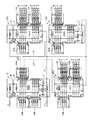
本実施形態では、上述したマスター装置2及びスレーブ装置3は各々、図2及び図3に示す電源ブロック6、通信ブロック7、制御ブロック8、9、入力ブロック10A、10B、出力ブロック11A、11Bを組み合わせて構成されている。各ブロック6〜11A、11B(回路ブロック)は、各々別々の基板上に設けられていて、これらを組み合わせて様々な形態の車載ネットワーク1を構成することができる。
In the present embodiment, the
図2に示す電源ブロック6は、電源Vp(例えば12V)を変換して後述する制御ブロック8、9への電源供給が可能な5V電源を生成するブロックである。電源ブロック6の基板には、電源端子T61と、グランド端子T62と、電源回路63と、5V電源端子T64と、が設けられている。
The
電源端子T61、グランド端子T62は、電源、グランドに接続される端子である。電源回路63は、電源端子T61に接続された電源Vpを変換して所定電圧(本実施形態では5V電源)を生成する回路である。5V電源端子T64は、電源回路63が生成した5V電源に接続される端子である。
The power supply terminal T61 and the ground terminal T62 are terminals connected to the power supply and the ground. The
図2に示す通信ブロック7は、後述する制御ブロック8、9間で通信を行うためのブロックである。通信ブロック7の基板には、複数の通信端子T71、T72と、通信IF回路73と、電源端子T74と、グランド端子T75と、が設けられている。本実施形態では、通信ブロック7には、2種類のLIN用の通信端子T71、CAN用の通信端子T72が設けられている。通信IF回路73は、上記通信端子T71、T72から各種通信(本実施形態ではCAN、LIN)に対応した信号の入出力を可能とするインタフェース回路である。電源端子T74、グランド端子T75は、グランド、電源に接続される端子である。これら端子T74、T75に接続された電源Vp、グランドは、通信IF回路73に供給される。
The
図3に示す制御ブロック8、9は、マスター装置2、スレーブ装置3の全体制御を司るブロックである。本実施形態では、制御ブロック8、9としては、マイコン84が実装されたマイコン制御ブロック8と、IC94が実装されたIC制御ブロック9と、の2種類がある。
The
マイコン制御ブロック8の基板は、電源端子T81と、グランド端子T82と、5V電源端子T83と、マイコン84と、複数の入力端子T85と、複数の出力端子T86と、複数の入力端子T87、通信端子T88、T89と、が設けられている。電源端子T81、グランド端子T82、5V電源端子T83は、電源、グランド、5V電源に接続される端子である。マイコン84は、入力ポートP11〜P18、出力ポートP21〜P28、ADポートP31〜P33や、図示しないPWM出力、タイマー、通信機能、RAM、CPU(Central Processing Unit)84A、フラッシュROM(Read Only Memory)84Bなどを内蔵している。
The board of the microcomputer control block 8 includes a power supply terminal T81, a ground terminal T82, a 5V power supply terminal T83, a
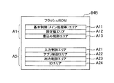
CPU84Aは、マスター装置2、スレーブ装置3全体の制御を司り、処理プログラムに従って各種の処理を行う。フラッシュROM84Bには、図5に示すように、後述する書込装置14による書き込み対象とならない書き込み対象外エリアA1と、後述する書込装置14による書き込み対象となる書き込み対象エリアA2と、が形成されている。
The
書き込み対象外エリアA1には、基本制御エリアA11と、設定値エリアA12と、書き込み制御エリアA13と、が形成されている。基本制御エリアA11には、通信等機能の設定や基本動作プログラムが記憶されている。設定値エリアA12には、各種設定値が記憶される。書き込み制御エリアA13には、後述する書き込み対象エリアA2に書き込みをするためのプログラムが記憶される。 A basic control area A11, a set value area A12, and a write control area A13 are formed in the write-out target area A1. In the basic control area A11, settings for functions such as communication and basic operation programs are stored. Various set values are stored in the set value area A12. In the write control area A13, a program for writing to the write target area A2, which will be described later, is stored.
書き込み対象エリアA2には、入力制御エリアA21と、アプリ制御エリアA22と、出力制御エリアA23と、IDエリアA24と、が形成されている。入力制御エリアA21には、入力ポートP11〜P18からの入力信号をもとに入力判定するプログラムが記憶される。アプリ制御エリアA22は、入力判定結果を入力判定データとして通信にて送信するプログラム、また通信によって受信した入力判定データをもとに負荷動作判定するプログラムが記憶される。出力制御エリアA23は、負荷動作判定結果をもとに出力信号を出力ポートP21〜P28から出力するプログラムが記憶される。IDエリアA24には、通信に必要なIDが記憶される。 An input control area A21, an application control area A22, an output control area A23, and an ID area A24 are formed in the write target area A2. In the input control area A21, a program for input determination based on the input signals from the input ports P11 to P18 is stored. The application control area A22 stores a program that transmits the input determination result as input determination data by communication, and a program that determines the load operation based on the input determination data received by communication. In the output control area A23, a program that outputs an output signal from the output ports P21 to P28 based on the load operation determination result is stored. An ID required for communication is stored in the ID area A24.
また、図3に示す複数の入力端子T85は、本実施形態では8つ設けられ、マイコン84の入力ポートP11〜P18に接続されている。複数の出力端子T86は、本実施形態では8つ設けられ、マイコン84の出力ポートP21〜P28に接続されている。複数の入力端子T87は、本実施形態では8つ設けられ、マイコン84のADポートP31〜P38に接続されている。通信端子T88、T89は、通信信号の入出力を行うための端子であり、本実施形態ではLIN用の通信端子T88と、CAN用の通信端子T89と、の2種類が設けられている。
In addition, eight of the plurality of input terminals T85 shown in FIG. 3 are provided in the present embodiment, and are connected to the input ports P11 to P18 of the
IC制御ブロック9は、スレーブ装置3の制御を司るブロックである。IC制御ブロック9の基板には、電源端子T91と、グランド端子T92と、5V電源端子T93と、IC94と、複数の入力端子T95と、複数の出力端子T96と、複数の入力端子T97と、通信端子T98と、が設けられている。
The
電源端子T91、グランド端子T92、5V電源端子T93は、電源、グランド、5V電源に接続される端子である。なお、後述するIC94に電源機能が内蔵されている場合は、5V電源端子T93は必要ない。IC94は、入力ポートP11〜P18、出力ポートP21〜P28、ADポートP31〜P38やCPU94Aを内蔵している。IC94は、周知のCPU94Aが内蔵され、通信機能及び電源機能の有無は使用するICによって異なる。従って、IC制御ブロック9単体で使用する場合や、IC制御ブロック9と通信ブロック7または電源ブロック6を組み合わせて使用する場合がある。IC94は、カスタムICまたは専用ICであり、IC内の制御仕様の書き込みはできない。
The power supply terminal T91, the ground terminal T92, and the 5V power supply terminal T93 are terminals connected to the power supply, ground, and 5V power supply. If the
また、複数の入力端子T95は、本実施形態では8つ設けられ、IC94の入力ポートP11〜P18に接続されている。複数の出力端子T96は、IC94の出力ポートP21〜P28に接続されている。入力端子T97は、IC94のADポートP31〜P38に接続されている。通信信号T98は、通信信号の入出力を行うための端子であり、本実施形態ではLIN用の通信端子T98が設けられている。 Further, eight plurality of input terminals T95 are provided in this embodiment and are connected to the input ports P11 to P18 of the IC94. The plurality of output terminals T96 are connected to the output ports P21 to P28 of the IC94. The input terminal T97 is connected to AD ports P31 to P38 of the IC94. The communication signal T98 is a terminal for inputting / outputting a communication signal, and in the present embodiment, a communication terminal T98 for LIN is provided.
図2に示す入力ブロック10A、10Bは、制御ブロック8、9の入力ポートP11〜P18に接続され、入力ポートP11〜P18に入力信号を入力するためのブロックである。入力ブロック10A、10Bの基板には、電源端子T101と、グランド端子T102と、複数のローカルスイッチSWと、複数の出力端子T103と、が形成されている。電源端子T101、グランド端子T102は、電源、グランドに接続される端子である。複数のローカルスイッチSWは、ユーザにより負荷5を動作させるためのスイッチである。本実施形態ではローカルスイッチSWは、制御ブロック8、9の入力端子T85、T95の数より少ない4つ設けられている。 The input blocks 10A and 10B shown in FIG. 2 are blocks connected to the input ports P11 to P18 of the control blocks 8 and 9 and for inputting an input signal to the input ports P11 to P18. A power supply terminal T101, a ground terminal T102, a plurality of local switch SWs, and a plurality of output terminals T103 are formed on the boards of the input blocks 10A and 10B. The power supply terminal T101 and the ground terminal T102 are terminals connected to the power supply and the ground. The plurality of local switch SWs are switches for operating the load 5 by the user. In this embodiment, four local switch SWs are provided, which is less than the number of input terminals T85 and T95 of the control blocks 8 and 9.
出力端子T103は、ローカルスイッチSWのオンオフ状態を出力するための端子であり、ローカルスイッチSWと同じ数、設けられている。本実施形態では、入力ブロック10A、10Bとしては、ローカルスイッチSWがオンしたとき出力端子T103からLo(グランド)が出力されるブロック10Aと、Hi(電源)が出力されるブロック10Bと、の2種類を例示している。なお、これに限らずHiが出力される出力端子T103とLoが出力される出力端子T103とが混在していてもよい。
The output terminals T103 are terminals for outputting the on / off state of the local switch SW, and are provided in the same number as the local switch SW. In the present embodiment, the input blocks 10A and 10B include a
出力ブロック11A、11Bは、制御ブロック8、9の出力ポートP21〜P28に接続され、出力信号に応じてオンオフする半導体リレーCH1〜CH4(出力スイッチ)が形成される。出力ブロック11A、11Bの基板には、電源端子T111と、グランド端子T112と、複数の半導体リレーCH1〜CH4と、複数の入力端子T113と、複数の出力端子T114、T115と、を有している。電源端子T111、グランド端子T112は、電源、グランドに接続される端子である。複数の半導体リレーCH1〜CH4は、例えば電流検出可能なIPDから構成されている。なお、複数の半導体リレーCH1〜CH4としては、これに限ったものではなく、メカリレー又は汎用MOSFETと、シャント抵抗で構成してもよいし、センスMOSFETから構成してもよい。
The output blocks 11A and 11B are connected to the output ports P21 to P28 of the control blocks 8 and 9, and semiconductor relays CH1 to CH4 (output switches) that are turned on and off according to the output signal are formed. The boards of the
複数の入力端子T113は、半導体リレーCH1〜CH4に対して1対1で設けられ、マイコン84やIC94からの出力信号が入力される。半導体リレーCH1〜CH4は、入力された出力信号に応じてオンオフする。複数の出力端子T114は、半導体リレーCH1〜CH4に対して1対1で設けられ、対応する半導体リレーCH1〜CH4がオンされたときに電源又はグランドが出力される。出力端子T115は、半導体リレーCH1〜CH4に対して1対1で設けられ、半導体リレーCH1〜CH4に流れる電流が検出電流として出力される端子である。
The plurality of input terminals T113 are provided on a one-to-one basis with respect to the semiconductor relays CH1 to CH4, and output signals from the
本実施形態では、出力ブロック11A、11Bとしては、半導体リレーCH1〜CH4がオンしたとき出力端子T115から電源が出力されるブロック11Aと、グランドが出力されるブロック11Bと、の2種類を例示している。
In the present embodiment, two types of
図4は、上述したブロックを組み合わせて構成した車載ネットワーク1の一例を示すブロック図である。同図に示すように、マスター装置2は、電源ブロック6と、通信ブロック7と、マイコン制御ブロック8と、2つの入力ブロック10A、10Bと、出力ブロック11Aと、から構成されている。
FIG. 4 is a block diagram showing an example of an in-
マスター装置2を構成する半導体リレーCH1〜CH3は、+B電源線L3、ACC電源線L4、IG電源線L5を介して+B用、ACC用、IG用のスレーブ装置301〜303に接続されている。半導体リレーCH4にはスレーブ装置3が接続されていない。半導体リレーCH1〜CH3は、マイコン84からの出力信号に応じてオンして、+B電源線L2からの電源を、+B電源線L3、ACC電源線L4、IG電源線L5を介して対応するスレーブ装置301〜303に供給する。
The semiconductor relays CH1 to CH3 constituting the
+B用のスレーブ装置301は、電源ブロック6と、IC制御ブロック9と、入力ブロック10Aと、出力ブロック11A、11Bと、から構成されている。スレーブ装置301に用いられるIC制御ブロック9には、通信機能が内蔵されており、通信ブロック7は必要ない。
The
ACC用のスレーブ装置302は、通信ブロック7と、IC制御ブロック9と、入力ブロック10Aと、出力ブロック11Aと、から構成されている。IC制御ブロック9には、電源機能が内蔵されており、電源ブロック6は必要ない。
The
IG用のスレーブ装置303は、IC制御ブロック9と、入力ブロック10Aと、出力ブロック11Aと、から構成されている。IC制御ブロック9には、電源機能、通信機能が内蔵されており、電源ブロック6、通信ブロック7は必要ない。
The
これらスレーブ装置301〜303を構成する半導体リレーCH1〜CH4は、負荷5に接続され、制御ブロック8、9からの出力信号に応じてオンして、負荷5に対して電源を供給する。
The semiconductor relays CH1 to CH4 constituting these
次に、上記マスター装置2及びスレーブ装置3間で授受される信号のビットアサイン(割り当て)を下記の表1を参照して説明する。

上記の表1に示すように、先頭のbit7〜bit0がマスター装置2、スレーブ装置3のIDを表す。IDは、車両4に配置されている全てのマスター装置2、スレーブ装置3に重複することなく割り振られる情報である。IDは、設置情報と、種別情報と、送受信情報と、スレーブ情報と、から構成されている。
As shown in Table 1 above, the
設置情報は、bit7〜bit4が割り当てられている。bit7〜bit6は、車両4の進行方向の設置位置を表し、スレーブ装置3の設置位置が車両4のフロント側であれば「01」、リア側であれば「10」、進行方向中央であれば「11」となる。bit5〜bi4は、車両4の左右方向の設置位置を表し、スレーブ装置3の設置位置が車両4の右側であれば「01」、左側であれば「10」、左右方向中央であれば「11」となる。
Bit7 to bit4 are assigned to the installation information. Bit7 to bit6 represent the installation position of the vehicle 4 in the traveling direction. If the installation position of the
種別情報は、bit3が割り当てられ、スレーブ装置3であれば「0」となり、マスター装置2であれば「1」となる。
As the type information,
送受信情報は、bit2が割り当てられ、スレーブ装置3がマスター装置2への送信する際は「1」となり、スレーブ装置3がマスター装置2から受信する際は「0」となる。
スレーブ情報は、bit1〜bit0が割り当てられている。スレーブ情報は、同一のマスター装置2に接続されている複数のスレーブ装置3に重複することなく割り振られる情報である(異なるマスター装置2に接続されているスレーブ装置3間では重複してもよい)。なお、本実施形態では、スレーブ情報は2ビットで表されているが、マスター装置2に接続されるスレーブ装置3の数に応じてビット数を増やしてもよい。
Bit1 to bit0 are assigned to the slave information. The slave information is information that is allocated to a plurality of
IDに続くbit7〜bit0のBYTE1は、ID設定後は入力判定データを表す。各bit7〜bit0はそれぞれ、複数の出力ポートP21〜P28に割り当てられている。そして、各bitn(nは0〜7の任意の整数)が「0」であればそのbitnに割り当てられた出力ポートP2(n+1)に接続された半導体リレーCH1〜CH4のオフを表す。各bitnが「1」であればそのbitnに割り当てられた出力ポートP2(n+1)に接続された半導体リレーCH1〜CH4のオンを表す。 BYTE1 of bit7 to bit0 following the ID represents input determination data after the ID is set. Each of bit7 to bit0 is assigned to a plurality of output ports P21 to P28, respectively. If each bitn (n is an arbitrary integer of 0 to 7) is "0", it means that the semiconductor relays CH1 to CH4 connected to the output port P2 (n + 1) assigned to the bitn are turned off. If each bitn is "1", it means that the semiconductor relays CH1 to CH4 connected to the output port P2 (n + 1) assigned to the bitn are turned on.
次に、上述した構成の車載ネットワーク1のID設定動作について図6及び図7のフローチャートを参照して説明する。なお、初期状態(ID未設定時)において、全てのマイコン制御ブロック8には、同じ初期ID(初期受信ID、初期送信ID)が設定されている。また、IC制御ブロック9は、図示しない外付けのスイッチの状態を確認してIDを認識するため、書込装置14でID設定する必要がない。
Next, the ID setting operation of the vehicle-mounted
書込装置14には、各エリアのマスター装置2のID、スレーブ装置3のIDが設定されている。また、書込装置14には、各スレーブ装置3がマイコン制御ブロック8で構成されているか、IC制御ブロック9で構成されているかが予め設定されている。
The
まず、ユーザは、通信ラインL1に書込装置14(図1)を接続する。書込装置14には、IDを設定したいエリアの順番が設定されている。例えば、図1に示す例では、FR−RH→RR−RH→RR−LH→FR−LH→FR−CENTERの順、またはFR−CENTER→FR−LH→RR−LH→RR−RH→FR−RHの順に通信ラインL1の対する接続順に設定されている。
First, the user connects the writing device 14 (FIG. 1) to the communication line L1. In the
書込装置14は、起動後、FR−RHエリアのID設定処理を実行する。ID設定処理において書込装置14は、ID付与要求信号を所定回数、送信する(ステップS101)。ID付与要求信号のビットアサインを下記の表2に示す。
表2に示すように、ID付与要求信号は、IDのbit7〜bit0が「0」となり、続くBYTE1にてID設定の必要な装置を設定する。本実施形態では、BYTE1のbit7がマスター装置2に割り当てられている。BYTE1のbit7には、マスター装置2のID設定を要求する場合は「1」が記憶され、ID設定を要求しない場合は「0」が記憶される。
As shown in Table 2, in the ID assignment request signal, the IDs bit7 to bit0 become "0", and the device that requires ID setting is set in the subsequent BYTE1. In this embodiment,
今、マスター装置2の出力ポートP21〜P24に接続されるスレーブ装置3をスレーブ装置301〜304とする。なお、図4に示す例ではスレーブ装置304については図示されていない。BYTE1のbit3〜bit0がマスター装置2の出力ポートP21〜P24に接続されているスレーブ装置301〜304に割り当てられている。BYTE1のbit3〜bit0には、スレーブ装置301〜304のID設定を要求する場合は「1」が記憶され、ID設定を要求しない場合は「0」が記憶される。また、BYTE1のbit6〜4は予備である。
Now, the
ステップS101において書込装置14は、まずマスター装置2のIDを設定するために、BYTE1のbit7のみが「1」となり、それ以外のbit6〜0を「0」としたID付与要求信号を送信する。
In step S101, the
その後、書込装置14は、所定時間T1経過するのを待って(ステップS102でY)、入力されたエリアのマスター装置2、スレーブ装置301〜304のIDを示す設定信号を送信する(ステップS103)。上記設定信号のビットアサインを下記の表3に示す。
設定信号は、IDのbit7〜bit0にマスター装置2の送信用ID、受信用IDの一方(実施形態では送信用ID)を設定し、その後のBYTE1〜BYTE4にマスター装置2の出力ポートP21〜P24に接続されるスレーブ装置301〜304のIDを設定している。即ち、マスター装置2に接続されるスレーブ装置3が4つあれば、最初のID、4つのBYTE1〜4が順次、設定信号として送信される。なお、図3に示す例では、マスター装置2に接続されるスレーブ装置301〜303は3つなので、表3とは異なり、スレーブ装置304に対応するBYTE4には初期値「0」が設定される。
As the setting signal, one of the transmission ID and the reception ID of the master device 2 (transmission ID in the embodiment) is set in the IDs bit7 to bit0, and the output ports P21 to P24 of the
表3に示す例では、IDのbit7〜bit4にフロント、右側を示す「0101」が設定される。また、IDのbit3にマスター装置2であることを示す「1」が記憶される。また、IDのbit2に送信用IDであることを示す「1」が記憶される。また、bit1〜bit0に「0」が記憶される。また、BYTE1〜4のbit7〜bit0にフロント、右側を示す「0101」が記憶される。また、BYTE1〜4のbit3にスレーブ装置3であることを示す「0」が記憶される。BYTE1〜4のbit3のbit2〜bit0にそれぞれ異なる値が記憶される。
In the example shown in Table 3, "0101" indicating the front side and the right side is set in bit7 to bit4 of the ID. Further, "1" indicating that it is the
また、ユーザは、IDを設定したいエリア順にマスター装置2を起動させる。最初は、FR−RHエリアのマスター装置2が起動される。起動後、マスター装置2のCPU84A(以下、単にマスター装置2ということもある)は、図6に示す処理を実行し、まずパワーオンリセット、初期処理を実行する(ステップS201、S202)。
In addition, the user activates the
その後、マスター装置2は、所定時間T2以内にマスター装置2に割り当てられたバイトのbit7が「1」、その他が「0」となるID設定要求信号を受信したか否かを判定する(ステップS203)。ID設定要求を受信していなければ(ステップS203でN)、マスター装置2は、通常処理を実行した後(ステップS204)、処理を終了する。
After that, the
一方、マスター装置2は、ID設定要求信号を受信すると(ステップS203でY)、次に設定信号を受信したか否かを判定する(ステップS205)。
On the other hand, when the
上記設定信号を受信すると(ステップS205でY)、マスター装置2は、設定信号のID部を自身のIDとして、フラッシュROM84B内に書き込む(ステップS206)。このとき、マスター装置2は、IDのbit2を反転させて、送信用ID、受信用IDの双方をフラッシュROM84Bに書き込む。これにより、マスター装置2のID認証が行われる。
Upon receiving the setting signal (Y in step S205), the
次に、マスター装置2は、BYTE1〜4をスレーブ装置301〜304のIDとして、フラッシュROM84B内に書き込む(ステップS207)。同様に、マスター装置2は、BYTEのbit2を反転させて、送信用ID、受信用IDの双方をフラッシュROM84Bに書き込む。
Next, the
図3に示す例では、マスター装置2は、書込装置14からID、BYTE1〜4から構成される設定信号を受信し、BYTE1〜3を出力ポートP21〜P23に接続されるスレーブ装置301〜303のIDとして、フラッシュROM84Bに書き込む。BYTE4は初期値なので書き込まない。
In the example shown in FIG. 3, the
その後、マスター装置2は、ID設定終了信号を送信する(ステップS208)。書込装置14は、設定信号の送信後(ステップS103)、所定時間T3内にID設定終了信号が受信できなければ(図7のステップS104でN)、処理を中止する(ステップS105)。一方、書込装置14は、設定信号の送信後(ステップS103)、所定時間T3内にID設定終了信号が受信できれば(ステップS104でY)、ID設定が必要なスレーブ装置3があるか否かを判定する(ステップS105)。
After that, the
書込装置14には、上述したようにスレーブ装置3がマイコン制御ブロック8から構成されているか、IC制御ブロック9から構成されているかが予めユーザによって入力されている。書込装置14は、IDを設定したいエリアのスレーブ装置3のうちマイコン制御ブロック8から構成されているスレーブ装置3があれば、ステップS105でID設定が必要なスレーブ装置3があると判定する。
As described above, the
図3に示すように全てのスレーブ装置301〜303がIC制御ブロック9から構成されている場合、書込装置14は、ID設定が必要なスレーブ装置3がないと判定し(ステップS105でN)、直ちにステップS113に進む。
When all the
一方、ID設定が必要なスレーブ装置3があると判定すると(ステップS105でY)、書込装置14は、マスター装置2の出力ポートP2n(nは任意の整数であり、初期状態では1に設定されている)に接続されたスレーブ装置30nのID設定が必要であるか否かを判定する(ステップS106)。書込装置14は、スレーブ装置30nがIC制御ブロック9で構成されたものであれば、IDの設定が必要ないと判定し(ステップS106でN)、ステップS111に進む。
On the other hand, when it is determined that there is a
書込装置14は、スレーブ装置30nがマイコン制御ブロック8で構成されたものであれば、IDの設定が必要であると判定し(ステップS106でY)、ID設定要求信号を所定回数送信する(ステップS107)。ID設定要求信号は、上記表2のビットアサインに従って、BYTE1のスレーブ装置30nに対応するbitnのみを「1」とした信号である。所定時間T4経過後(ステップS108でY)、書込装置14は、IDエリアにスレーブ装置30nに対応するIDを設定し、BYTE1〜BYTE4に「0」を設定した設定信号を送信する(ステップS109)。なお、スレーブ装置301に対する設定信号は下記の表4に示すようになる。
ID設定終了信号送信後(図6のステップS208)、マスター装置2は、ID設定要求信号を受信できなければ(図7のステップS209でN)、全ての半導体リレーCH1〜CH4をオフした後(ステップS210)、ステップS212に進む。
After transmitting the ID setting end signal (step S208 in FIG. 6), if the
マスター装置2は、ID設定要求信号を受信すると(ステップS209でY)、「1」となっているbitnに対応する半導体リレーCHnをオンした後(ステップS211)、ステップS212に進む。
When the
これにより、半導体リレーCHnに接続されたスレーブ装置30nに電源が供給され、スレーブ装置30nが起動する。起動後、スレーブ装置30nは、パワーオンリセット、初期化処理を実行した後(ステップS301、S302)、所定時間T5内にID設定要求信号を受信したか否かを判定する(ステップS303)。所定時間T5内にID設定要求を受信できなければ(ステップS303でN)、スレーブ装置30nは、通常処理を実行した後(ステップS304)、処理を終了する。 As a result, power is supplied to the slave device 30n connected to the semiconductor relay CHn, and the slave device 30n is activated. After activation, the slave device 30n determines whether or not the ID setting request signal has been received within the predetermined time T5 after executing the power-on reset and initialization processing (steps S301 and S302) (step S303). If the ID setting request cannot be received within the predetermined time T5 (N in step S303), the slave device 30n ends the process after executing the normal process (step S304).
一方、所定時間T5内にID設定要求を受信できれば(ステップS303でY)、スレーブ装置30nは、設定信号を受信できたか否かを判定する(ステップS305)。スレーブ装置30nは、設定信号が受信できれば(ステップS305でY)、設定信号のID部を自身のIDとしてフラッシュROM84Bに書き込む(ステップS306)。その後、スレーブ装置30nはID設定終了信号を送信した後(ステップS307)、処理を終了する。
On the other hand, if the ID setting request can be received within the predetermined time T5 (Y in step S303), the slave device 30n determines whether or not the setting signal can be received (step S305). If the slave device 30n can receive the set signal (Y in step S305), the slave device 30n writes the ID portion of the set signal as its own ID in the
書込装置14は、設定信号送信後(ステップS109)、所定時間T6内にスレーブ装置30nからID設定終了信号を受信できなければ(ステップS110でN)、処理を終了する(ステップS105)。一方、書込装置14は、所定時間T6内にスレーブ装置30nからID設定終了信号を受信すると(ステップS110でY)、ステップS111に進む。
If the
ステップS111において、書込装置14は、ID設定が必要な全てのスレーブ装置3へのID設定が終了したか否かを判定する。書込装置14は、終了していないと判定すると(ステップS111でN)、nをインクリメントした後(ステップS112)、直ちにステップS106に戻る。
In step S111, the
一方、書込装置14は、終了していると判定すると(ステップS111でY)、ID設定完了信号を送信した後(ステップS113)、処理を終了する。マスター装置2は、ID設定完了信号を受信すると(ステップS212でY)、直ちに処理を終了する。一方、マスター装置2は、ID設定完了信号を受信していなければ(ステップS212でN)、ステップS209に戻る。
On the other hand, when the
書込装置14は、FR−RHエリアに対応した上述したステップS101〜S113を実行した後、次のエリアに対応した上述したステップS101〜S113を順次、実行する。ユーザは、これに応じてエリアに対応するスレーブ装置3を起動させる。これにより、マスター装置2及びスレーブ装置3にIDを設定することができる。
The
上述した実施形態によれば、マスター装置2及び複数のスレーブ装置3が、複数種類のブロック6〜11A、11Bを組み合わせて構成されているので、機能変更や設計変更が発生した場合、ブロック6〜11A、11B単位で交換したり、追加することができ、コストダウンを図ることができる。
According to the above-described embodiment, the
上述した実施形態によれば、ブロックとしては、スレーブ装置3又はマスター装置2の制御を司る制御ブロック8、9と、制御ブロック8、9の入力ポートP11〜P18に接続され、当該入力ポートP11〜P18に入力信号を入力するための入力ブロック10A、10Bと、制御ブロック8、9の出力ポートP21〜P28に接続され、出力信号に応じてオンオフする半導体リレーCH1〜CH4を有する出力ブロック11A、11Bと、を含んでいる。
According to the above-described embodiment, the blocks are connected to the control blocks 8 and 9 that control the
これにより、機能変更や設計変更が発生した場合、制御ブロック8、9、入力ブロック10A、10B、出力ブロック11A、11B単位で交換したり、追加することで、コストダウンを図ることができる。また、入力信号を入力するための素子や、半導体リレーCH1〜CH4数を最小限に抑えることができる。
As a result, when a function change or a design change occurs, the cost can be reduced by exchanging or adding the control blocks 8 and 9, the input blocks 10A and 10B, and the
また、上述した実施形態によれば、ブロックとしては、制御ブロック8、9に電源を供給するための電源ブロック6と、通信インタフェースを有する通信ブロック7と、を含んでいる。これにより、電源機能や通信機能を有していない制御ブロック8、9も用いることができ、他製品で開発された設計資産を流用することができる。
Further, according to the above-described embodiment, the block includes a
また、上述した実施形態によれば、マスター装置2は、書込装置14から当該マスター装置2のIDを受信して自身のIDとして設定する。また、マスター装置2は、自身のID設定後、書込装置14から複数のスレーブ装置3のIDを受信する毎に半導体リレーCH1〜CH4を順にオンする。複数のスレーブ装置3は、電源供給後に受信したIDを自身のIDとして設定する。これにより、スレーブ装置3を接続する(組み付ける)毎にIDを付与する必要がないため、IDの設定時間の短縮を図ると共に、誤設定を低減できる。
Further, according to the above-described embodiment, the
また、上述した実施形態によれば、マスター装置2は、車両4内に設置され、複数のスレーブ装置3は、複数の負荷5に接続されている。複数の負荷5は、常時駆動可能な負荷5と、アクセサリ時に駆動可能な負荷5と、イグニッション時に駆動可能な負荷5と、に分類されている。そして、1つのスレーブ装置3には、同一種類の負荷5が接続されている。これにより、スレーブ装置3に電源供給して、負荷5を駆動可能にするための半導体リレーCH1〜CH4を利用して、IDの設定を行うことができる。
Further, according to the above-described embodiment, the
上述した実施形態によれば、マスター装置2は、車両4内に複数設置され、フラッシュROM24Bに記憶されたIDは、マスター装置2の車両4内での設置位置を示す設置情報を含む。これにより、車両4に設定されたスレーブ装置3に容易にそれぞれ別々のIDを付与することができる。
According to the above-described embodiment, a plurality of
なお、上述した実施形態によれば、入力ブロック10A、10Bは、ローカルスイッチSWから構成されていたが、これに限ったものではない。入力ブロック10A、10Bとしては、制御ブロック8、9に入力信号を入力できるものであればよく、例えば、センサなどから構成されていてもよい。 According to the above-described embodiment, the input blocks 10A and 10B are composed of the local switch SW, but the present invention is not limited to this. The input blocks 10A and 10B may be any as long as they can input input signals to the control blocks 8 and 9, and may be composed of, for example, a sensor.
また、上述した実施形態によれば、スレーブ装置3及びマスター装置2が、電源ブロック6、通信ブロック7、制御ブロック8、9、入力ブロック10A、10B、出力ブロック11A、11Bを組み合わせて構成されていたが、これに限ったものではない。制御ブロック8、9として、電源機能、通信機能を有するものを用いれば、制御ブロック8、9、入力ブロック10A、10B、出力ブロック11A、11Bのみを組み合わせて構成してもよい。
Further, according to the above-described embodiment, the
また、上述した実施形態によれば、書込装置14が、スレーブ装置301〜30nのIDを送信していたが、これに限ったものではない。マスター装置2がスレーブ装置301〜30nのIDを順次送信するようにしてもよい。
Further, according to the above-described embodiment, the
なお、本発明は上記実施形態に限定されるものではない。即ち、本発明の骨子を逸脱しない範囲で種々変形して実施することができる。 The present invention is not limited to the above embodiment. That is, it can be modified in various ways without departing from the gist of the present invention.
1 車載ネットワーク(通信システム)
2 マスター装置
3、301〜303 スレーブ装置
4 車両
5 負荷
6 電源ブロック(回路ブロック)
7 通信ブロック(回路ブロック)
8、9 制御ブロック(回路ブロック)
10A、10B 入力ブロック(回路ブロック)
11A、11B 出力ブロック(回路ブロック)
14 書込装置
84A CPU(第1設定部、スイッチ制御部、第2設定部)
CH1〜CH4 半導体リレー(出力スイッチ)
P11〜P18 入力ポート
P21〜P28 出力ポート
1 In-vehicle network (communication system)
2
7 Communication block (circuit block)
8, 9 control block (circuit block)
10A, 10B input block (circuit block)
11A, 11B output block (circuit block)
14
CH1 to CH4 semiconductor relay (output switch)
P11 to P18 input port P21 to P28 output port
Claims (5)
各々機能が異なり、別々の基板上に形成された複数種類の回路ブロックを備え、
前記スレーブ装置及び前記マスター装置が、前記複数種類の回路ブロックを組み合わせて構成され、
前記通信システムは、前記スレーブ装置及び前記マスター装置にIDを書き込むための書込装置をさらに備え、
前記書込装置は、前記マスター装置のIDを送信した後、当該マスター装置に通信可能に接続された複数のスレーブ装置のIDを順次送信し、
前記マスター装置は、当該マスター装置に通信可能に接続された通信可能に接続された複数のスレーブ装置に電源を供給するための複数の出力スイッチと、前記書込装置から当該マスター装置のIDを受信して自身のIDとして設定する第1設定部と、自身のID設定後、当該マスター装置に通信可能に接続された通信可能に接続された複数の複数のスレーブ装置のIDを前記書込装置から受信する毎に前記出力スイッチを順にオンするスイッチ制御部と、を有し、
前記スレーブ装置は、電源供給後に受信した前記IDを自身のIDとして設定する第2設定部を有することを特徴とする通信システム。 A communication system comprising one or more master devices, each of which is communicably connected to a plurality of slave devices.
Each has different functions and has multiple types of circuit blocks formed on different boards.
The slave device and the master device are configured by combining the plurality of types of circuit blocks.
The communication system further includes a writing device for writing an ID to the slave device and the master device.
After transmitting the ID of the master device, the writing device sequentially transmits the IDs of a plurality of slave devices communicably connected to the master device.
The master device receives a plurality of output switches for supplying power to a plurality of communicably connected slave devices connected to the master device, and an ID of the master device from the writing device. The IDs of the first setting unit, which is set as its own ID, and the IDs of a plurality of communicably connected slave devices, which are communicably connected to the master device after setting its own ID, are transmitted from the writing device. It has a switch control unit that turns on the output switch in order each time it is received.
The slave device is a communication system including a second setting unit that sets the ID received after power supply as its own ID.
前記マスター装置のIDは、前記マスター装置の車両内での設置位置を示す設置情報を含むことを特徴とする請求項1または2に記載の通信システム。 A plurality of the master devices are installed in the vehicle,
The communication system according to claim 1 or 2 , wherein the ID of the master device includes installation information indicating an installation position of the master device in a vehicle.
Priority Applications (4)
| Application Number | Priority Date | Filing Date | Title |
|---|---|---|---|
| JP2018196432A JP6865202B2 (en) | 2018-10-18 | 2018-10-18 | Communications system |
| US16/559,857 US11082253B2 (en) | 2018-10-18 | 2019-09-04 | Communication system |
| EP19202952.8A EP3640091B1 (en) | 2018-10-18 | 2019-10-14 | In-vehicle communication system |
| CN201910994452.9A CN111083673B (en) | 2018-10-18 | 2019-10-18 | Communication system |
Applications Claiming Priority (1)
| Application Number | Priority Date | Filing Date | Title |
|---|---|---|---|
| JP2018196432A JP6865202B2 (en) | 2018-10-18 | 2018-10-18 | Communications system |
Publications (2)
| Publication Number | Publication Date |
|---|---|
| JP2020065189A JP2020065189A (en) | 2020-04-23 |
| JP6865202B2 true JP6865202B2 (en) | 2021-04-28 |
Family
ID=68295949
Family Applications (1)
| Application Number | Title | Priority Date | Filing Date |
|---|---|---|---|
| JP2018196432A Active JP6865202B2 (en) | 2018-10-18 | 2018-10-18 | Communications system |
Country Status (4)
| Country | Link |
|---|---|
| US (1) | US11082253B2 (en) |
| EP (1) | EP3640091B1 (en) |
| JP (1) | JP6865202B2 (en) |
| CN (1) | CN111083673B (en) |
Families Citing this family (5)
| Publication number | Priority date | Publication date | Assignee | Title |
|---|---|---|---|---|
| DE102020215527A1 (en) * | 2020-12-09 | 2022-06-09 | Robert Bosch Gesellschaft mit beschränkter Haftung | Vehicle with a zone architecture |
| DE102020215525A1 (en) * | 2020-12-09 | 2022-06-09 | Robert Bosch Gesellschaft mit beschränkter Haftung | Vehicle with a zone architecture |
| DE102020215524A1 (en) * | 2020-12-09 | 2022-06-09 | Robert Bosch Gesellschaft mit beschränkter Haftung | Vehicle with a zone architecture |
| DE102020215529A1 (en) * | 2020-12-09 | 2022-06-09 | Robert Bosch Gesellschaft mit beschränkter Haftung | Vehicle with a zone architecture |
| GB2603798A (en) | 2021-02-15 | 2022-08-17 | Vitesco Tech Gmbh | Automotive network zoned architecture with failure mitigation feature |
Family Cites Families (14)
| Publication number | Priority date | Publication date | Assignee | Title |
|---|---|---|---|---|
| US5305316A (en) * | 1990-09-04 | 1994-04-19 | Nissan Motor Co., Ltd. | Multiplex communication system |
| DE10055163B4 (en) * | 2000-11-08 | 2013-01-03 | Bayerische Motoren Werke Aktiengesellschaft | Data bus, especially in motor vehicles |
| EP2207103A1 (en) | 2004-04-01 | 2010-07-14 | Panasonic Corporation | Integrated circuit for video/audio processing |
| JP4211683B2 (en) * | 2004-05-28 | 2009-01-21 | 株式会社デンソー | Communications system |
| JP2005335607A (en) | 2004-05-28 | 2005-12-08 | Calsonic Kansei Corp | In-vehicle instrument control system and master device of on-vehicle network |
| JP2007215102A (en) * | 2006-02-13 | 2007-08-23 | Denso Corp | Communication device |
| JP4973858B2 (en) * | 2007-06-12 | 2012-07-11 | オムロン株式会社 | IO unit |
| JP5363379B2 (en) * | 2009-05-20 | 2013-12-11 | ルネサスエレクトロニクス株式会社 | Communications system |
| JP2012038040A (en) | 2010-08-05 | 2012-02-23 | Auto Network Gijutsu Kenkyusho:Kk | Processing system, processing unit, and power supply control method |
| KR102210890B1 (en) * | 2013-06-05 | 2021-02-02 | 삼성에스디아이 주식회사 | Battery management system, and method of managing the same |
| US20160277208A1 (en) * | 2015-03-18 | 2016-09-22 | GM Global Technology Operations LLC | Vehicle communication system |
| JP6535201B2 (en) * | 2015-04-17 | 2019-06-26 | 矢崎総業株式会社 | Connecting member and vehicle network system |
| JP6383348B2 (en) * | 2015-12-22 | 2018-08-29 | 矢崎総業株式会社 | Control device and control system |
| JP6905499B2 (en) * | 2018-10-18 | 2021-07-21 | 矢崎総業株式会社 | Communications system |
-
2018
- 2018-10-18 JP JP2018196432A patent/JP6865202B2/en active Active
-
2019
- 2019-09-04 US US16/559,857 patent/US11082253B2/en active Active
- 2019-10-14 EP EP19202952.8A patent/EP3640091B1/en active Active
- 2019-10-18 CN CN201910994452.9A patent/CN111083673B/en active Active
Also Published As
| Publication number | Publication date |
|---|---|
| EP3640091B1 (en) | 2023-08-02 |
| JP2020065189A (en) | 2020-04-23 |
| CN111083673A (en) | 2020-04-28 |
| US20200127870A1 (en) | 2020-04-23 |
| US11082253B2 (en) | 2021-08-03 |
| EP3640091A1 (en) | 2020-04-22 |
| CN111083673B (en) | 2023-06-06 |
Similar Documents
| Publication | Publication Date | Title |
|---|---|---|
| JP6865202B2 (en) | Communications system | |
| US10780783B2 (en) | Onboard vehicle communication system | |
| US10887128B2 (en) | In-vehicle network system | |
| US9166910B2 (en) | Data relay apparatus | |
| CN110395197B (en) | Communication system | |
| WO2019035261A1 (en) | Control device, control method and computer program | |
| JP6905499B2 (en) | Communications system | |
| CN109789849A (en) | The determining equipment of positioning is carried out to mobile access mechanism on vehicle | |
| WO2013046700A1 (en) | Vehicle data setting system and output setting method thereof | |
| JP5905162B2 (en) | Sensor structure for electrical / electronic architecture and corresponding electrical / electronic architecture for vehicles | |
| CN108243244B (en) | Vehicle-mounted communication system and control method thereof | |
| EP3640811B1 (en) | Communication system | |
| CN103457813B (en) | Aftermarket module arrangement and method for communicating over a vehicle bus | |
| US20130241280A1 (en) | Touch Activated, Wireless Switches | |
| JP6587510B2 (en) | In-vehicle communication system | |
| JP5359449B2 (en) | Relay system and control device | |
| JP7046700B2 (en) | Communications system | |
| JP6568456B2 (en) | In-vehicle communication system | |
| CN111356994B (en) | Modular computer architecture for a cockpit and infotainment system of a vehicle | |
| WO2021111925A1 (en) | Vehicle-mounted system, vehicle-mounted information registration device, and information registration method | |
| WO2011007429A1 (en) | Communication device, navigation device and communication system |
Legal Events
| Date | Code | Title | Description |
|---|---|---|---|
| A621 | Written request for application examination |
Free format text: JAPANESE INTERMEDIATE CODE: A621 Effective date: 20191119 |
|
| A977 | Report on retrieval |
Free format text: JAPANESE INTERMEDIATE CODE: A971007 Effective date: 20200924 |
|
| A131 | Notification of reasons for refusal |
Free format text: JAPANESE INTERMEDIATE CODE: A131 Effective date: 20201110 |
|
| A521 | Request for written amendment filed |
Free format text: JAPANESE INTERMEDIATE CODE: A523 Effective date: 20201214 |
|
| TRDD | Decision of grant or rejection written | ||
| A01 | Written decision to grant a patent or to grant a registration (utility model) |
Free format text: JAPANESE INTERMEDIATE CODE: A01 Effective date: 20210330 |
|
| A61 | First payment of annual fees (during grant procedure) |
Free format text: JAPANESE INTERMEDIATE CODE: A61 Effective date: 20210405 |
|
| R150 | Certificate of patent or registration of utility model |
Ref document number: 6865202 Country of ref document: JP Free format text: JAPANESE INTERMEDIATE CODE: R150 |
|
| S531 | Written request for registration of change of domicile |
Free format text: JAPANESE INTERMEDIATE CODE: R313531 |
|
| R350 | Written notification of registration of transfer |
Free format text: JAPANESE INTERMEDIATE CODE: R350 |
|
| R250 | Receipt of annual fees |
Free format text: JAPANESE INTERMEDIATE CODE: R250 |