JP6854088B2 - Optical effects of aerodynamic ultrastructure - Google Patents
Optical effects of aerodynamic ultrastructure Download PDFInfo
- Publication number
- JP6854088B2 JP6854088B2 JP2016080285A JP2016080285A JP6854088B2 JP 6854088 B2 JP6854088 B2 JP 6854088B2 JP 2016080285 A JP2016080285 A JP 2016080285A JP 2016080285 A JP2016080285 A JP 2016080285A JP 6854088 B2 JP6854088 B2 JP 6854088B2
- Authority
- JP
- Japan
- Prior art keywords
- microstructure
- sub
- microstructures
- group
- exemplary
- Prior art date
- Legal status (The legal status is an assumption and is not a legal conclusion. Google has not performed a legal analysis and makes no representation as to the accuracy of the status listed.)
- Active
Links
- 230000003287 optical effect Effects 0.000 title claims description 26
- 238000000034 method Methods 0.000 claims description 37
- 238000004049 embossing Methods 0.000 claims description 13
- 238000000576 coating method Methods 0.000 claims description 6
- 230000008859 change Effects 0.000 claims description 5
- 239000011248 coating agent Substances 0.000 claims description 5
- 238000002310 reflectometry Methods 0.000 claims 1
- 230000015654 memory Effects 0.000 description 18
- 238000003860 storage Methods 0.000 description 18
- 230000000694 effects Effects 0.000 description 17
- 238000010586 diagram Methods 0.000 description 10
- 230000008569 process Effects 0.000 description 10
- 230000007704 transition Effects 0.000 description 9
- 230000000007 visual effect Effects 0.000 description 8
- 238000004519 manufacturing process Methods 0.000 description 6
- 230000015572 biosynthetic process Effects 0.000 description 5
- 239000002086 nanomaterial Substances 0.000 description 5
- 230000000737 periodic effect Effects 0.000 description 5
- CURLTUGMZLYLDI-UHFFFAOYSA-N Carbon dioxide Chemical compound O=C=O CURLTUGMZLYLDI-UHFFFAOYSA-N 0.000 description 4
- 238000003754 machining Methods 0.000 description 4
- 239000000463 material Substances 0.000 description 4
- 239000003381 stabilizer Substances 0.000 description 4
- 230000005540 biological transmission Effects 0.000 description 3
- 238000005266 casting Methods 0.000 description 3
- 238000000465 moulding Methods 0.000 description 3
- 230000001902 propagating effect Effects 0.000 description 3
- 230000003139 buffering effect Effects 0.000 description 2
- 229910002092 carbon dioxide Inorganic materials 0.000 description 2
- 239000001569 carbon dioxide Substances 0.000 description 2
- 239000012530 fluid Substances 0.000 description 2
- 239000000446 fuel Substances 0.000 description 2
- 230000006870 function Effects 0.000 description 2
- 238000003384 imaging method Methods 0.000 description 2
- 230000007774 longterm Effects 0.000 description 2
- 239000003973 paint Substances 0.000 description 2
- 229920000642 polymer Polymers 0.000 description 2
- 230000003334 potential effect Effects 0.000 description 2
- 238000012545 processing Methods 0.000 description 2
- 230000009467 reduction Effects 0.000 description 2
- 238000004904 shortening Methods 0.000 description 2
- 239000000243 solution Substances 0.000 description 2
- 241000272517 Anseriformes Species 0.000 description 1
- 241000699670 Mus sp. Species 0.000 description 1
- 238000010521 absorption reaction Methods 0.000 description 1
- 230000002411 adverse Effects 0.000 description 1
- 239000006117 anti-reflective coating Substances 0.000 description 1
- 230000002457 bidirectional effect Effects 0.000 description 1
- 230000001413 cellular effect Effects 0.000 description 1
- 239000003086 colorant Substances 0.000 description 1
- 238000009500 colour coating Methods 0.000 description 1
- 238000004891 communication Methods 0.000 description 1
- 230000000295 complement effect Effects 0.000 description 1
- 239000002131 composite material Substances 0.000 description 1
- 238000013461 design Methods 0.000 description 1
- 239000006185 dispersion Substances 0.000 description 1
- 238000009826 distribution Methods 0.000 description 1
- 230000007613 environmental effect Effects 0.000 description 1
- 238000005530 etching Methods 0.000 description 1
- 238000001125 extrusion Methods 0.000 description 1
- 239000007888 film coating Substances 0.000 description 1
- 238000009501 film coating Methods 0.000 description 1
- 238000005286 illumination Methods 0.000 description 1
- 238000002347 injection Methods 0.000 description 1
- 239000007924 injection Substances 0.000 description 1
- 238000007689 inspection Methods 0.000 description 1
- 230000001788 irregular Effects 0.000 description 1
- 230000031700 light absorption Effects 0.000 description 1
- 239000004973 liquid crystal related substance Substances 0.000 description 1
- 238000012986 modification Methods 0.000 description 1
- 230000004048 modification Effects 0.000 description 1
- 230000002028 premature Effects 0.000 description 1
- 238000000926 separation method Methods 0.000 description 1
- 230000003595 spectral effect Effects 0.000 description 1
- 238000005507 spraying Methods 0.000 description 1
- 238000013517 stratification Methods 0.000 description 1
- 238000005728 strengthening Methods 0.000 description 1
- 230000007847 structural defect Effects 0.000 description 1
- 239000000758 substrate Substances 0.000 description 1
- 230000001360 synchronised effect Effects 0.000 description 1
- 238000003856 thermoforming Methods 0.000 description 1
- 238000012546 transfer Methods 0.000 description 1
- 230000001052 transient effect Effects 0.000 description 1
- 238000002834 transmittance Methods 0.000 description 1
- 238000012795 verification Methods 0.000 description 1
- 238000011179 visual inspection Methods 0.000 description 1
Images


Classifications
-
- B—PERFORMING OPERATIONS; TRANSPORTING
- B64—AIRCRAFT; AVIATION; COSMONAUTICS
- B64C—AEROPLANES; HELICOPTERS
- B64C21/00—Influencing air flow over aircraft surfaces by affecting boundary layer flow
- B64C21/10—Influencing air flow over aircraft surfaces by affecting boundary layer flow using other surface properties, e.g. roughness
-
- G—PHYSICS
- G06—COMPUTING; CALCULATING OR COUNTING
- G06F—ELECTRIC DIGITAL DATA PROCESSING
- G06F30/00—Computer-aided design [CAD]
- G06F30/10—Geometric CAD
- G06F30/15—Vehicle, aircraft or watercraft design
-
- B—PERFORMING OPERATIONS; TRANSPORTING
- B42—BOOKBINDING; ALBUMS; FILES; SPECIAL PRINTED MATTER
- B42D—BOOKS; BOOK COVERS; LOOSE LEAVES; PRINTED MATTER CHARACTERISED BY IDENTIFICATION OR SECURITY FEATURES; PRINTED MATTER OF SPECIAL FORMAT OR STYLE NOT OTHERWISE PROVIDED FOR; DEVICES FOR USE THEREWITH AND NOT OTHERWISE PROVIDED FOR; MOVABLE-STRIP WRITING OR READING APPARATUS
- B42D25/00—Information-bearing cards or sheet-like structures characterised by identification or security features; Manufacture thereof
- B42D25/30—Identification or security features, e.g. for preventing forgery
- B42D25/324—Reliefs
-
- B—PERFORMING OPERATIONS; TRANSPORTING
- B32—LAYERED PRODUCTS
- B32B—LAYERED PRODUCTS, i.e. PRODUCTS BUILT-UP OF STRATA OF FLAT OR NON-FLAT, e.g. CELLULAR OR HONEYCOMB, FORM
- B32B27/00—Layered products comprising a layer of synthetic resin
- B32B27/06—Layered products comprising a layer of synthetic resin as the main or only constituent of a layer, which is next to another layer of the same or of a different material
- B32B27/08—Layered products comprising a layer of synthetic resin as the main or only constituent of a layer, which is next to another layer of the same or of a different material of synthetic resin
-
- B—PERFORMING OPERATIONS; TRANSPORTING
- B32—LAYERED PRODUCTS
- B32B—LAYERED PRODUCTS, i.e. PRODUCTS BUILT-UP OF STRATA OF FLAT OR NON-FLAT, e.g. CELLULAR OR HONEYCOMB, FORM
- B32B3/00—Layered products comprising a layer with external or internal discontinuities or unevennesses, or a layer of non-planar shape; Layered products comprising a layer having particular features of form
- B32B3/26—Layered products comprising a layer with external or internal discontinuities or unevennesses, or a layer of non-planar shape; Layered products comprising a layer having particular features of form characterised by a particular shape of the outline of the cross-section of a continuous layer; characterised by a layer with cavities or internal voids ; characterised by an apertured layer
- B32B3/30—Layered products comprising a layer with external or internal discontinuities or unevennesses, or a layer of non-planar shape; Layered products comprising a layer having particular features of form characterised by a particular shape of the outline of the cross-section of a continuous layer; characterised by a layer with cavities or internal voids ; characterised by an apertured layer characterised by a layer formed with recesses or projections, e.g. hollows, grooves, protuberances, ribs
-
- B—PERFORMING OPERATIONS; TRANSPORTING
- B44—DECORATIVE ARTS
- B44B—MACHINES, APPARATUS OR TOOLS FOR ARTISTIC WORK, e.g. FOR SCULPTURING, GUILLOCHING, CARVING, BRANDING, INLAYING
- B44B5/00—Machines or apparatus for embossing decorations or marks, e.g. embossing coins
- B44B5/0047—Machines or apparatus for embossing decorations or marks, e.g. embossing coins by rolling
-
- B—PERFORMING OPERATIONS; TRANSPORTING
- B44—DECORATIVE ARTS
- B44B—MACHINES, APPARATUS OR TOOLS FOR ARTISTIC WORK, e.g. FOR SCULPTURING, GUILLOCHING, CARVING, BRANDING, INLAYING
- B44B5/00—Machines or apparatus for embossing decorations or marks, e.g. embossing coins
- B44B5/0095—Machines or apparatus for embossing decorations or marks, e.g. embossing coins using computer control means
-
- B—PERFORMING OPERATIONS; TRANSPORTING
- B44—DECORATIVE ARTS
- B44F—SPECIAL DESIGNS OR PICTURES
- B44F1/00—Designs or pictures characterised by special or unusual light effects
- B44F1/02—Designs or pictures characterised by special or unusual light effects produced by reflected light, e.g. matt surfaces, lustrous surfaces
-
- B—PERFORMING OPERATIONS; TRANSPORTING
- B64—AIRCRAFT; AVIATION; COSMONAUTICS
- B64C—AEROPLANES; HELICOPTERS
- B64C23/00—Influencing air flow over aircraft surfaces, not otherwise provided for
-
- B—PERFORMING OPERATIONS; TRANSPORTING
- B64—AIRCRAFT; AVIATION; COSMONAUTICS
- B64D—EQUIPMENT FOR FITTING IN OR TO AIRCRAFT; FLIGHT SUITS; PARACHUTES; ARRANGEMENT OR MOUNTING OF POWER PLANTS OR PROPULSION TRANSMISSIONS IN AIRCRAFT
- B64D45/00—Aircraft indicators or protectors not otherwise provided for
-
- G—PHYSICS
- G06—COMPUTING; CALCULATING OR COUNTING
- G06V—IMAGE OR VIDEO RECOGNITION OR UNDERSTANDING
- G06V20/00—Scenes; Scene-specific elements
- G06V20/60—Type of objects
- G06V20/69—Microscopic objects, e.g. biological cells or cellular parts
-
- G—PHYSICS
- G09—EDUCATION; CRYPTOGRAPHY; DISPLAY; ADVERTISING; SEALS
- G09F—DISPLAYING; ADVERTISING; SIGNS; LABELS OR NAME-PLATES; SEALS
- G09F19/00—Advertising or display means not otherwise provided for
- G09F19/12—Advertising or display means not otherwise provided for using special optical effects
- G09F19/14—Advertising or display means not otherwise provided for using special optical effects displaying different signs depending upon the view-point of the observer
-
- G—PHYSICS
- G09—EDUCATION; CRYPTOGRAPHY; DISPLAY; ADVERTISING; SEALS
- G09F—DISPLAYING; ADVERTISING; SIGNS; LABELS OR NAME-PLATES; SEALS
- G09F21/00—Mobile visual advertising
- G09F21/06—Mobile visual advertising by aeroplanes, airships, balloons, or kites
- G09F21/08—Mobile visual advertising by aeroplanes, airships, balloons, or kites the advertising matter being arranged on the aircraft
-
- B—PERFORMING OPERATIONS; TRANSPORTING
- B32—LAYERED PRODUCTS
- B32B—LAYERED PRODUCTS, i.e. PRODUCTS BUILT-UP OF STRATA OF FLAT OR NON-FLAT, e.g. CELLULAR OR HONEYCOMB, FORM
- B32B2250/00—Layers arrangement
- B32B2250/02—2 layers
-
- B—PERFORMING OPERATIONS; TRANSPORTING
- B32—LAYERED PRODUCTS
- B32B—LAYERED PRODUCTS, i.e. PRODUCTS BUILT-UP OF STRATA OF FLAT OR NON-FLAT, e.g. CELLULAR OR HONEYCOMB, FORM
- B32B2250/00—Layers arrangement
- B32B2250/03—3 layers
-
- B—PERFORMING OPERATIONS; TRANSPORTING
- B32—LAYERED PRODUCTS
- B32B—LAYERED PRODUCTS, i.e. PRODUCTS BUILT-UP OF STRATA OF FLAT OR NON-FLAT, e.g. CELLULAR OR HONEYCOMB, FORM
- B32B2250/00—Layers arrangement
- B32B2250/24—All layers being polymeric
-
- B—PERFORMING OPERATIONS; TRANSPORTING
- B32—LAYERED PRODUCTS
- B32B—LAYERED PRODUCTS, i.e. PRODUCTS BUILT-UP OF STRATA OF FLAT OR NON-FLAT, e.g. CELLULAR OR HONEYCOMB, FORM
- B32B2255/00—Coating on the layer surface
- B32B2255/10—Coating on the layer surface on synthetic resin layer or on natural or synthetic rubber layer
-
- B—PERFORMING OPERATIONS; TRANSPORTING
- B32—LAYERED PRODUCTS
- B32B—LAYERED PRODUCTS, i.e. PRODUCTS BUILT-UP OF STRATA OF FLAT OR NON-FLAT, e.g. CELLULAR OR HONEYCOMB, FORM
- B32B2307/00—Properties of the layers or laminate
- B32B2307/40—Properties of the layers or laminate having particular optical properties
- B32B2307/402—Coloured
-
- B—PERFORMING OPERATIONS; TRANSPORTING
- B32—LAYERED PRODUCTS
- B32B—LAYERED PRODUCTS, i.e. PRODUCTS BUILT-UP OF STRATA OF FLAT OR NON-FLAT, e.g. CELLULAR OR HONEYCOMB, FORM
- B32B2307/00—Properties of the layers or laminate
- B32B2307/40—Properties of the layers or laminate having particular optical properties
- B32B2307/412—Transparent
-
- B—PERFORMING OPERATIONS; TRANSPORTING
- B32—LAYERED PRODUCTS
- B32B—LAYERED PRODUCTS, i.e. PRODUCTS BUILT-UP OF STRATA OF FLAT OR NON-FLAT, e.g. CELLULAR OR HONEYCOMB, FORM
- B32B2307/00—Properties of the layers or laminate
- B32B2307/40—Properties of the layers or laminate having particular optical properties
- B32B2307/414—Translucent
-
- B—PERFORMING OPERATIONS; TRANSPORTING
- B32—LAYERED PRODUCTS
- B32B—LAYERED PRODUCTS, i.e. PRODUCTS BUILT-UP OF STRATA OF FLAT OR NON-FLAT, e.g. CELLULAR OR HONEYCOMB, FORM
- B32B2307/00—Properties of the layers or laminate
- B32B2307/40—Properties of the layers or laminate having particular optical properties
- B32B2307/416—Reflective
-
- B—PERFORMING OPERATIONS; TRANSPORTING
- B32—LAYERED PRODUCTS
- B32B—LAYERED PRODUCTS, i.e. PRODUCTS BUILT-UP OF STRATA OF FLAT OR NON-FLAT, e.g. CELLULAR OR HONEYCOMB, FORM
- B32B2307/00—Properties of the layers or laminate
- B32B2307/50—Properties of the layers or laminate having particular mechanical properties
- B32B2307/538—Roughness
-
- B—PERFORMING OPERATIONS; TRANSPORTING
- B32—LAYERED PRODUCTS
- B32B—LAYERED PRODUCTS, i.e. PRODUCTS BUILT-UP OF STRATA OF FLAT OR NON-FLAT, e.g. CELLULAR OR HONEYCOMB, FORM
- B32B2605/00—Vehicles
- B32B2605/18—Aircraft
-
- B—PERFORMING OPERATIONS; TRANSPORTING
- B41—PRINTING; LINING MACHINES; TYPEWRITERS; STAMPS
- B41M—PRINTING, DUPLICATING, MARKING, OR COPYING PROCESSES; COLOUR PRINTING
- B41M3/00—Printing processes to produce particular kinds of printed work, e.g. patterns
-
- B—PERFORMING OPERATIONS; TRANSPORTING
- B64—AIRCRAFT; AVIATION; COSMONAUTICS
- B64C—AEROPLANES; HELICOPTERS
- B64C2230/00—Boundary layer controls
- B64C2230/26—Boundary layer controls by using rib lets or hydrophobic surfaces
-
- F—MECHANICAL ENGINEERING; LIGHTING; HEATING; WEAPONS; BLASTING
- F15—FLUID-PRESSURE ACTUATORS; HYDRAULICS OR PNEUMATICS IN GENERAL
- F15D—FLUID DYNAMICS, i.e. METHODS OR MEANS FOR INFLUENCING THE FLOW OF GASES OR LIQUIDS
- F15D1/00—Influencing flow of fluids
- F15D1/002—Influencing flow of fluids by influencing the boundary layer
- F15D1/0025—Influencing flow of fluids by influencing the boundary layer using passive means, i.e. without external energy supply
- F15D1/003—Influencing flow of fluids by influencing the boundary layer using passive means, i.e. without external energy supply comprising surface features, e.g. indentations or protrusions
- F15D1/0035—Influencing flow of fluids by influencing the boundary layer using passive means, i.e. without external energy supply comprising surface features, e.g. indentations or protrusions in the form of riblets
-
- G—PHYSICS
- G06—COMPUTING; CALCULATING OR COUNTING
- G06F—ELECTRIC DIGITAL DATA PROCESSING
- G06F2113/00—Details relating to the application field
- G06F2113/28—Fuselage, exterior or interior
-
- Y—GENERAL TAGGING OF NEW TECHNOLOGICAL DEVELOPMENTS; GENERAL TAGGING OF CROSS-SECTIONAL TECHNOLOGIES SPANNING OVER SEVERAL SECTIONS OF THE IPC; TECHNICAL SUBJECTS COVERED BY FORMER USPC CROSS-REFERENCE ART COLLECTIONS [XRACs] AND DIGESTS
- Y02—TECHNOLOGIES OR APPLICATIONS FOR MITIGATION OR ADAPTATION AGAINST CLIMATE CHANGE
- Y02T—CLIMATE CHANGE MITIGATION TECHNOLOGIES RELATED TO TRANSPORTATION
- Y02T50/00—Aeronautics or air transport
- Y02T50/10—Drag reduction
Landscapes
- Engineering & Computer Science (AREA)
- Physics & Mathematics (AREA)
- General Physics & Mathematics (AREA)
- Theoretical Computer Science (AREA)
- Aviation & Aerospace Engineering (AREA)
- Business, Economics & Management (AREA)
- Accounting & Taxation (AREA)
- Marketing (AREA)
- General Engineering & Computer Science (AREA)
- Geometry (AREA)
- Computer Hardware Design (AREA)
- Biomedical Technology (AREA)
- Mathematical Optimization (AREA)
- Pure & Applied Mathematics (AREA)
- Computational Mathematics (AREA)
- Evolutionary Computation (AREA)
- Automation & Control Theory (AREA)
- Health & Medical Sciences (AREA)
- Life Sciences & Earth Sciences (AREA)
- Mathematical Analysis (AREA)
- General Health & Medical Sciences (AREA)
- Molecular Biology (AREA)
- Multimedia (AREA)
- Optical Elements Other Than Lenses (AREA)
- Surface Treatment Of Optical Elements (AREA)
- Fluid Mechanics (AREA)
- Mechanical Engineering (AREA)
- Manufacturing & Machinery (AREA)
- Vehicle Interior And Exterior Ornaments, Soundproofing, And Insulation (AREA)
- Transportation (AREA)
Description
本発明は概して微細構造に関し、より具体的には空気力学的微細構造の光学的効果に関する。 The present invention relates generally to microstructures, and more specifically to the optical effects of aerodynamic microstructures.
微細構造は典型的に、航空機の飛行特性及び/又は飛行力学を変えるため、航空機上で使用される。特に、リブレットなどの微細構造は、航空機翼、尾翼部又は胴体の表面上で、航空機の抗力又は抗力係数を低減するために使用され、これによって、全体的な燃料節約及び/又は二酸化炭素排出低減などをもたらすことができる。しかしながら、リブレット及び他の微細構造はまた、高い反射率、指向性反射を含む特定の光学的/美的/視覚的な効果、及び/又はその幾何形状により航空機の美観にその他の潜在的な効果をもたらす又は妨げることがありうる。高い反射率及び関連する指向性反射は、しばしばグリント(glint)と称されるが、航空機の視認性及び/又は美観に影響を及ぼすことがありうる。リブレットは、典型的な航空機表面(例えば、翼表面、胴体表面など)と比較して、その幾何学的配置、形状及び/又は外観によって、不規則な方向にグリントを引き起こしうる。 Ultrastructures are typically used on aircraft to alter the flight characteristics and / or flight dynamics of the aircraft. In particular, microstructures such as riblets are used to reduce the drag or drag coefficient of the aircraft on the surface of the aircraft wing, tail or airframe, thereby saving overall fuel and / or reducing carbon dioxide emissions. And so on. However, riblets and other microstructures also have certain optical / aesthetic / visual effects, including high reflectance, directional reflections, and / or other potential effects on the aesthetics of the aircraft due to their geometry. It can bring or hinder. High reflectance and associated directional reflections, often referred to as glints, can affect the visibility and / or aesthetics of the aircraft. Riblets can cause glint in irregular directions due to their geometric arrangement, shape and / or appearance compared to typical aircraft surfaces (eg, wing surfaces, fuselage surfaces, etc.).
ある状況においては、航空機の反射率及び/又は全体的な外観は、航空機の種々の部分の反射率及び/又は反射角を調整することによって制御されうる。航空機の外観に効果を与えるための既知の解決策には、平坦な黒色塗装又は多層フィルムコーティングなどの低反射率光学コーティングが含まれている。航空機の反射率及び/又は外観を変えるための他の既知の解決策には転写シールが含まれるが、これらをリブレットなどの空気力学的表面に貼付すると、リブレットの空気力学的特性に悪影響を及ぼし、その結果、リブレットの効果を低下させる。 In some situations, the reflectance and / or overall appearance of the aircraft can be controlled by adjusting the reflectance and / or angle of reflection of various parts of the aircraft. Known solutions for affecting the appearance of aircraft include low reflectance optical coatings such as flat black paint or multilayer film coatings. Other known solutions for altering aircraft reflectance and / or appearance include transfer seals, but applying these to aerodynamic surfaces such as riblets adversely affects the aerodynamic properties of riblets. As a result, the effect of riblets is reduced.
例示的な装置は、ビークルの外部表面を画定する空気力学的微細構造、及び画像の表現を伝えるため微細構造の上に重ね合わせられたサブ微細構造のパターンを含む。 An exemplary device includes an aerodynamic microstructure that defines the outer surface of the vehicle, and a pattern of sub-microstructures that are overlaid on top of the microstructure to convey the representation of the image.
例示的な方法は、微細構造の外部表面の上にサブ微細構造の第1グループを設けることを含む。例示的な方法はまた、外部表面上又は外部表面近傍にサブ微細構造の第2グループを設けることを含み、光学的な効果を作り出すため、サブ微細構造の第2グループは、サブ微細構造の第1グループとは異なるように配向され、離間され、形作られ或いは整列される。 An exemplary method comprises providing a first group of sub-microstructures on the outer surface of the microstructure. An exemplary method also comprises providing a second group of sub-ultrastructures on or near the outer surface to create an optical effect, so that the second group of sub-ultrastructures is a second group of sub-ultrastructures. Oriented, separated, shaped or aligned differently than one group.
別の例示的な方法は、航空力学的微細構造の表面に適用される画像を受け取り、受け取った画像に基づいて、表面上に受け取った画像の表現を作り出すように表面上にサブ微細構造のパターンを設けることを含む。 Another exemplary method is to take an image applied to the surface of an aerodynamic microstructure and, based on the received image, create a representation of the received image on the surface with a pattern of sub-microstructures on the surface. Includes the provision of.
別の例示的な装置は、航空機の外部表面を画定する航空力学的微細構造を含む。例示的な航空力学的微細構造は、航空力学的微細構造の上に重ね合わせられた第1のサブ微細構造グループを含む。例示的な航空力学的微細構造はまた、航空力学的微細構造の上に重ね合わせられ、第1のサブ微細構造グループとは異なる第2のサブ微細構造グループを含み、第1及び第2のサブ微細構造グループの組み合わせが画像の表現を伝える。 Another exemplary device includes an aerodynamic microstructure that defines the outer surface of the aircraft. An exemplary aerodynamic ultrastructure includes a first sub-ultrastructure group overlaid on top of the aerodynamic ultrastructure. The exemplary aerodynamic microstructure also includes a second sub-ultrastructure group that is superposed on top of the aerodynamic microstructure and is different from the first sub-ultrastructure group, the first and second sub-structures. The combination of microstructure groups conveys the representation of the image.
本発明の一実施形態は、ビークルの外部表面を画定する空気力学的微細構造、及び画像の表現を伝えるため微細構造の上に重ね合わせられたサブ微細構造のパターンを含む。サブ微細構造のパターンは、サブ微細構造の第1及び第2グループを含むことがあり、サブ微細構造の第2グループはサブ微細構造の第1グループとは異なる。サブ微細構造の第2グループは、サブ微細構造の第1グループと比較して、異なる形状、間隔、又は配向を有しうる。サブ微細構造のパターンは、サブ微細構造及び外部表面の比較的平坦な部分を含みうる。サブ微細構造のパターンにおけるサブ微細構造間の間隔は、性能を高めるため、光の波長にほぼ等しくなりうる。サブ微細構造のパターンにおけるサブ微細構造の表面は、反射性コーティングで被覆されうる。特定の条件下で性能を確実なものにするため、サブ微細構造のパターンにおけるサブ微細構造間の間隔は、約0.4ミクロン未満になりうる。また、装置は外部表面の近傍にカラー層を含みうる。 One embodiment of the invention includes an aerodynamic microstructure defining the outer surface of the vehicle and a pattern of sub-microstructures overlaid on top of the microstructure to convey the representation of the image. The pattern of the sub-ultrastructure may include first and second groups of the sub-ultrastructure, the second group of the sub-ultrastructure is different from the first group of the sub-ultrastructure. The second group of sub-ultrastructures may have different shapes, spacings, or orientations as compared to the first group of sub-ultrastructures. The pattern of the sub-ultrastructure may include the sub-ultrastructure and a relatively flat portion of the outer surface. The spacing between the sub-ultrastructures in the sub-ultrastructure pattern can be approximately equal to the wavelength of light to enhance performance. The surface of the sub-ultrastructure in the sub-ultrastructure pattern can be coated with a reflective coating. To ensure performance under certain conditions, the spacing between substructures in the pattern of substructures can be less than about 0.4 microns. The device may also include a color layer in the vicinity of the outer surface.
本発明の別の実施形態は、微細構造の外部表面上にサブ微細構造の第1グループを設けること、及び外部表面上又は外部表面近傍にサブ微細構造の第2グループを設けることを含む方法に関連し、光学的な効果を作り出すため、サブ微細構造の第2グループは、サブ微細構造の第1グループとは異なるように配向され、離間され、形作られ或いは整列されている。外部表面は、複数の微細構造に広がりうる。サブ微細構造の第1及び第2グループを設けることは、外部表面の上にサブ微細構造をエンボス加工することを含みうる。方法はまた、サブ微細構造の第1グループを設けるためツールを整列すること、及びサブ微細構造の第2グループを設けるためツールを再整列又は移動することを含みうる。第1又は第2のサブ微細構造グループのサブ微細構造間の間隔は、約0.4〜0.7ミクロンとなりうる。 Another embodiment of the present invention comprises providing a first group of sub-microstructures on the outer surface of the microstructure and providing a second group of sub-microstructures on or near the outer surface. Related and to create an optical effect, the second group of sub-ultrastructures is oriented, separated, shaped or aligned differently than the first group of sub-ultrastructures. The outer surface can spread over multiple microstructures. Providing the first and second groups of sub-microstructures may include embossing the sub-microstructures on the outer surface. The method may also include aligning the tools to provide a first group of sub-microstructures and rearranging or moving the tools to provide a second group of sub-microstructures. The spacing between the sub-microstructures of the first or second sub-microstructure group can be about 0.4-0.7 microns.
本発明の別の実施形態は、航空力学的微細構造の表面に適用される画像を受け取り、受け取った画像に基づいて、表面上に受け取った画像の表現を作り出すように表面上にサブ微細構造のパターンを設けることを含む。サブ微細構造を設けることは、表面上の種々の場所に寸法の異なるサブ微細構造を設けるようにツールを配向することを含みうる。サブ微細構造のパターンにおけるサブ微細構造は、放物線形状、三角形状、溝型形状、正弦波形状、円錐形状、円筒形状、又は複数の段形状のうちの一又は複数を有しうる。サブ微細構造のパターンにおけるサブ微細構造間の間隔は、約0.4〜0.7ミクロンとなりうる。 Another embodiment of the invention receives an image applied to the surface of an aerodynamic microstructure and, based on the received image, sub-microstructures on the surface to create a representation of the received image on the surface. Includes providing a pattern. Providing the sub-microstructure may include orienting the tool to provide sub-microstructures of different dimensions at various locations on the surface. The sub-ultrastructure in the pattern of the sub-ultrastructure can have one or more of a parabolic shape, a triangular shape, a grooved shape, a sinusoidal shape, a conical shape, a cylindrical shape, or a plurality of stepped shapes. The spacing between sub-ultrastructures in the pattern of sub-ultrastructures can be about 0.4-0.7 microns.
本発明の別の実施形態は、航空力学的構造の上に重ね合わせられた第1のサブ微細構造グループと、航空力学的構造の上に重ね合わせられ、第1のサブ微細構造グループとは異なる第2のサブ微細構造グループと、画像の表現を伝えるための第1及び第2の微細構造グループの組み合わせとを含む、航空機の外部表面を画定する航空力学的微細構造を含む装置に関する。第2のサブ微細構造グループは、サブ微細構造の第1グループと比較して、異なる形状、間隔、又は配向を有しうる。装置はまた、画像の表現を少なくとも部分的に伝えるため、航空力学的微細構造の平坦な部分を含みうる。 Another embodiment of the present invention differs from the first sub-ultrastructure group superimposed on the aerodynamic structure and the first sub-ultrastructure group superimposed on the aerodynamic structure. It relates to a device comprising an aerodynamic microstructure defining the outer surface of an aircraft, including a second sub-microstructure group and a combination of first and second microstructure groups for conveying the representation of an image. The second sub-ultrastructure group may have a different shape, spacing, or orientation as compared to the first group of sub-ultrastructures. The device may also include a flat portion of the aerodynamic ultrastructure to convey at least a partial representation of the image.
図面及び添付の記載の全体を通して、可能な箇所にはすべて、同じ部分又は類似の部分を指すために同じ参照番号が使用される。本開示において使用される、任意の部分が、任意の方式で、別の部分の(例えば、上に配置される、上に位置する、上に設置される、上に形成される、など)の表現は、言及される部分がもう一方の部分と接触している、又は、言及される部分が、もう一方との間に一又は複数の中間部分を伴ってもう一方の部分の上部にある、のいずれをも意味する。任意の部分が別の部分と接触しているとの表現は、当該2つの部分の間に中間部分がないことを意味する。 Throughout the drawings and accompanying descriptions, the same reference numbers are used to refer to the same or similar parts wherever possible. As used in the present disclosure, any part, in any manner, of another part (eg, placed on, located on, placed on, formed on, etc.) The expression is that the mentioned part is in contact with the other part, or the mentioned part is above the other part with one or more intermediate parts between it and the other. Means any of. The expression that any part is in contact with another means that there is no intermediate part between the two parts.
航空力学的微細構造の光学的効果が本明細書に開示されている。例えば、リブレットなどの微細構造は典型的に、飛行特性を改変及び/又は改善して、航空機の全体的な抗力を低減するため、航空機の空気力学的表面上で使用される。これによって、例えば、全体的な燃料節約及び/又は二酸化炭素排出低減などをもたらすことができる。但し、これらのリブレット及び他の空気力学的微細構造はまた、特定の角度及び/又は視角での反射率の変化を含む、関連の及び/又は意図しない光学的/視覚的効果を引き起こすことがあり、その結果、望ましくないグリント及び/又は航空機の美観にその他の潜在的な影響(例えば、光沢、色彩効果、色の歪みなど)をもたらす。 The optical effects of aerodynamic ultrastructure are disclosed herein. For example, microstructures such as riblets are typically used on the aerodynamic surface of an aircraft to modify and / or improve flight characteristics and reduce the overall drag of the aircraft. This can result in, for example, overall fuel savings and / or reduced carbon dioxide emissions. However, these riblets and other aerodynamic microstructures can also cause related and / or unintended optical / visual effects, including changes in reflectance at certain angles and / or viewing angles. As a result, it brings about unwanted glint and / or other potential effects on the aesthetics of the aircraft (eg, gloss, color effects, color distortion, etc.).
航空機及び/又はリブレットなどの航空機に関連する外部微細構造は、仕上げられ、滑らかになった及び/又は研磨された表面を有する。これらの表面は反射率が高く、グリントを引き起こしうる及び/又は航空機の全体的な外観に影響を及ぼしうるフレネル反射をもたらすことがある。しかしながら、本開示の教示に従い、リブレットの種々の反射性の表面及び/又は隣接する反射性の表面は、表面の種々の部分がパターンに応じて異なるように反射する光学的効果によって、画像の表現及び/又はロゴマークを伝えるパターンを画定するように使用されうる。 Aircraft and / or aircraft-related external microstructures such as riblets have a finished, smoothed and / or polished surface. These surfaces are highly reflective and can result in Fresnel reflections that can cause glint and / or affect the overall appearance of the aircraft. However, according to the teachings of the present disclosure, the various reflective surfaces of the riblets and / or adjacent reflective surfaces are represented by an optical effect in which different parts of the surface reflect differently depending on the pattern. And / or can be used to define a pattern that conveys the logo mark.
本明細書に開示の実施例は、サブ微細構造(例えば、ナノ構造)及び/又はサブ微細構造パターンを利用するが、これらは、例えば、微細構造によって引き起こされうる反射(例えば、フレネル反射など)及び/又は反射率の変化を制御するため、微細構造(例えば、外部の空気力学的微細構造)の上又は下に重ね合わせられたナノスケール(例えば、寸法がおよそ10−9メートル単位)となることもあれば、ならないこともある。特に、サブ微細構造のパターン(例えば、散在する比較的平坦な部分を含む又は含まないサブ微細構造、及び/又は種々のサブ微細構造部分)が、この制御のために使用されうる。幾つかの実施例では、実施例が実装される微細構造はビークル(例えば、航空機、地上ビークル、潜水艦など)に適用されるリブレットである。これらのリブレットは、ビークルの抗力係数低減に利用される。幾つかの実施例では、比較的平坦な部分に沿ったサブ微細構造は、例示的な微細構造が設けられるビークル(例えば、航空機)の表面又は外観の光学特性及び/又は美観をカスタマイズするために使用される。 The examples disclosed herein utilize sub-microstructures (eg, nanostructures) and / or sub-microstructure patterns, which are, for example, reflections that can be caused by microstructures (eg, Fresnel reflections, etc.). And / or nanoscales (eg, dimensions approximately 10-9 meters) overlaid on or under the microstructure (eg, external aerodynamic microstructure) to control changes in reflectance. Sometimes it doesn't. In particular, patterns of sub-microstructures (eg, sub-microstructures with or without interspersed relatively flat parts, and / or various sub-ultrastructure parts) can be used for this control. In some embodiments, the microstructure in which the embodiments are implemented is a riblet applied to a vehicle (eg, aircraft, ground vehicle, submarine, etc.). These riblets are used to reduce the drag coefficient of the vehicle. In some embodiments, the sub-microstructure along a relatively flat portion is used to customize the optical properties and / or aesthetics of the surface or appearance of a vehicle (eg, an aircraft) provided with an exemplary microstructure. used.
本明細書に開示の実施例は、様々な場所又は位置から反射及び/又はグリントを低減又は増大させて、所望の光学的効果を実現するため、ビークルの表面の特定の領域での反射を含む外観の制御を可能にする。また、本明細書に開示の実施例により、ビークルのカスタマイズされた光学的効果を実装することができる。特に、幾つかの実施例で、例えば、ビークルの可視外部表面の一部に対する特定の位置及び/又は視角での反射率又は透過率を制限すること或いは高めることによって、ロゴマーク及び/又はカラー層などの特定の美的外観は所定の角度から見ることが可能になる。カラー層が使用される実施例では、カラー層は、種々の装飾的効果及び/又は反射効果のため、微細構造に機械的に連結されてもよく、微細構造に一体化されてもよく、及び/又はサブ微細構造と共に使用されてもよい。幾つかの実施例では、カラー層及び/又は微細構造は、光屈折効果及び/又は、微細構造及び/又は微細構造内に埋め込まれた層(例えば、カラー層)からの回折効果など、種々の光学的、美的及び/又は装飾的効果のため、カラー層と微細構造との間の界面特性(例えば、テクスチャ加工された表面)を有しうる。 The embodiments disclosed herein include reflections at specific regions of the surface of the vehicle in order to reduce or increase reflections and / or glint from various locations or locations to achieve the desired optical effect. Allows control of appearance. Also, the examples disclosed herein can implement customized optical effects of the vehicle. In particular, in some embodiments, the logo mark and / or color layer, for example, by limiting or increasing the reflectance or transmittance at a particular location and / or viewing angle with respect to a portion of the vehicle's visible outer surface. Certain aesthetic appearances, such as, can be viewed from a given angle. In embodiments where color layers are used, the color layers may be mechanically coupled to or integrated into the microstructure for various decorative and / or reflective effects, and / Or may be used with sub-microstructures. In some embodiments, the color layer and / or microstructure has a variety of effects, such as a light refraction effect and / or a diffraction effect from a layer (eg, a color layer) embedded within the microstructure and / or microstructure. It may have interfacial properties (eg, textured surfaces) between the color layer and the microstructure for optical, aesthetic and / or decorative effects.
幾つかの実施例では、微細構造の外観を修正するため、サブ微細構造及び/又はサブ微細構造のグループが、機械加工又は他の任意の適切な処理によって、微細構造の上に設けられる。特に、サブ微細構造は、例えば、ロール形成又はエンボス加工処理によって、微細構造の上に形成されうる。本明細書に開示の幾つかの実施例では、サブ微細構造は、微細構造が押し出されるにつれて(例えば、インライン二次処理)、微細構造の上に形成される。サブ微細構造を設けること及び/又は作成することは、直接的な表面修正によって、或いはロール形成又はエンボス加工のためのツールの作成によって間接的に、或いは押出成形、鋳造、吹き付け、エッチングなどによって行われうる。 In some embodiments, a group of sub-microstructures and / or sub-microstructures is provided on top of the microstructure by machining or any other suitable treatment to modify the appearance of the microstructure. In particular, the sub-ultrastructure can be formed on top of the microstructure, for example by roll forming or embossing. In some embodiments disclosed herein, the sub-microstructure is formed on top of the microstructure as it is extruded (eg, in-line secondary treatment). Sub-microstructures are provided and / or created by direct surface modification, indirectly by the creation of tools for roll formation or embossing, or by extrusion, casting, spraying, etching, etc. It can be done.
本明細書で使用されているように、「微細構造」という用語は、幾何学的特徴、寸法、及び/又は、およそ10〜200ミクロン、典型的には75〜125ミクロンのサイズを有する、幾何学的特徴の間の間隔(例えば、周期的な間隔、高さ及び/又は幅など)を示すことがある。本明細書で使用されているように、「サブ微細構造」という用語は、幾何学的特徴(例えば、周期的又は非周期的な間隔、高さ及び/又は幅など)が微細構造よりも大幅に小さくなる、幾何学的特徴、寸法及び/又は間隔を示すことがある。これらの実施例では、サブ微細構造はおよそ0.1〜10ミクロンのサイズを有しうる。「ナノ構造」と称されることもある幾つかのサブ微細構造は、約0.4〜0.7ミクロンで、ほぼ可視光の波長以下のサイズ及び/又は間隔の範囲に及ぶ。したがって、「サブ微細構造」という用語はまた、約0.4ミクロン未満の寸法を示すことがある。そのため、本明細書で使用されている「微細構造」及び「サブ微細構造」という用語に関しては、「ほぼ光の波長」という表現は、約0.1〜10ミクロンの範囲に及ぶ寸法を意味する。 As used herein, the term "microstructure" has geometric features, dimensions, and / or a size of approximately 10 to 200 microns, typically 75 to 125 microns. It may indicate the spacing between geometric features (eg, periodic spacing, height and / or width, etc.). As used herein, the term "sub-microstructure" has significantly more geometric features (eg, periodic or aperiodic spacing, height and / or width, etc.) than microstructure. May show smaller geometric features, dimensions and / or spacing. In these examples, the sub-microstructure can have a size of approximately 0.1-10 microns. Some sub-ultrastructures, sometimes referred to as "nanostructures," are about 0.4-0.7 microns and range in size and / or spacing well below the wavelength of visible light. Therefore, the term "sub-ultrastructure" may also refer to dimensions less than about 0.4 microns. Therefore, with respect to the terms "ultrastructure" and "sub-ultrastructure" used herein, the expression "almost wavelength of light" means dimensions ranging from about 0.1 to 10 microns. ..
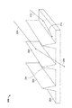
図1は、本明細書に開示の実施例が実装されうる例示的な航空機100を示す。図解例の航空機100は、背側フェアリング104に隣接した垂直尾翼102、水平安定板106を含む尾部101、機首部分(例えば、コクピット部分)110及び胴体114に取り付けられた翼112を含む。本明細書に記載の実施例は、尾部101、機首部分110、安定板106、翼112及び/又は胴体114のいずれかの表面及び/又は外観、或いはその他の外装又は機外構造体(例えば、翼ストラット、エンジンストラット、先尾翼安定板など)及び/又は表面に適用されうる。
FIG. 1 shows an
図2は、本明細書に開示の実施例が実装されうる、図1の例示的な航空機100の外部表面の例示的な微細構造200である。図解例の微細構造200は、互いに離間されているリッジ202、及びリッジ202を互いに離間するベース表面(例えば、谷、航空機表面など)204を含む。この実施例では、リッジ202の輪郭は概して三角形で、その結果、概して三角形の断面を有するリッジを画定する。微細構造200の輪郭は、微細構造200(例えば、微細構造200の画定された容積)を画定するように押出成形される。この実施例では、例示的な微細構造200が押出成形されるが、例示的な微細構造200はエンボス加工、鋳造、加圧成形、熱成形、機械加工などによって成形されうる。他の実施例では、ベース表面204は、グリントを制御するため、リッジ202よりも小さいリッジ(例えば、リッジ202の高さの3分の1未満)を有しうる。
FIG. 2 is an
この実施例では、微細構造200は航空機100のリブレットで、航空機100の抗力全体を低減することによって、航空機100の空気力学特性を変えるために使用されるもので、例えば、航空機100の任意の外部表面に配置されうる。図解例の微細構造200は、航空機100の外部表面に近い大気中で、乱流境界層を制御すること、及び/又は乱流境界層に関連する交差流を防止することによって、空気力学的抗力を低減するために使用される。特に、例示的な微細構造200はリッジ202を有し、航空機100の外部表面に取り付けられ、所望の気流の方向に整列されている。この整列により、リッジ202は、外部表面付近で横方向の気流の動きを分断する小さなフェンス又はガイドとして動作することが可能になり、一列に並んだ乱流を強化し、外部表面の外板摩擦を低減し、これによって航空機100の全体的な抗力を低減する。幾つかの実施例では、微細構造200は、航空機100の製造中又は製造後に、外部表面に装着、又は取り付けられることはなく、外部表面に一体化されている。例えば、微細構造200は、外部表面に連結(例えば、機械的に接着)されるのではなく、外部表面上にあらかじめ形成(例えば、外板表面に機械加工又は鋳造、複合材硬化部品に組み込み、ロボットにより配置)される。
In this embodiment, the
微細構造200の全体的な幾何形状は、一般的に、指向性(例えば、前方散乱又は後方散乱)のある反射、及び/又はグリントとして知られる光学的現象を引き起こしうる。これは航空機100の全体的な外観に影響を及ぼしうる。グリントは、光が表面付近である角度(例えば、面法線から離れた入射角)で表面に当たるときに、最も一般的に発生し、これによって、微細構造200の表面及び/又は小表面から、微細構造200及び航空機100に対してある視角及び/又は位置に向かって、前方に(例えば、前方散乱)光線を反射させる。入射光は、直接照明によって、或いは別の表面からの反射によって、表面に当たる。幾つかの実施例では、この反射率は微細構造200に対して特定の視角及び/又は位置でグリントを引き起こし、これにより、航空機100の全体的な外観に影響を及ぼしうる。図2に示すように、入射光線206はリッジ表面にほぼ平行にリッジ202の1つに当たり、その結果、反射208はベース表面204に向かって前方に進み、反射光線208はベース表面で吸収、透過、又は反射される。同様に、光線210は、例えば、ベース表面204からリッジ202の1つの表面に向かう反射212を引き起こしうる。反射208、212は、表面をかすめ(法線から離れた角度で表面に当たり)、航空機100の好ましくない及び/又は意図しない外観を引き起こす入射光から生ずる反射であるため、グレージング角光反射と称されることもある。
The overall geometry of the
図3は、本開示の教示に従い、重ね合わせられたサブ微細構造(例えば、ナノリッジ、サブ微細構造パターンなど)を有する微細構造(例えば、リブレット、押出リブレット)300の断面図である。図解例の微細構造300は、先端305を有する遠位部分304、中間部分306及びベース部分308を含む、種々の部分を有する。この例では、遠位部分304は移行部分310によって中間部分306から分離されており、ここで、サブ微細構造は1つのサイズから別のサイズに移行しうる(例えば、徐々に移行する)。移行部分310はサブ微細構造312を有し、中間部分306はサブ微細構造314を有する。同様に、図解例のベース部分308はサブ微細構造316を有する。幾つかの実施例では、先端305は小さすぎるため、先端305の上に重ね合わせられたサブ微細構造を有することはできない。但し、幾つかの実施例では、ナノスケールのサブ微細構造が先端305の近傍及び/又は先端305の上に重ね合わせられうる。
FIG. 3 is a cross-sectional view of a microstructure (eg, riblet, extruded riblet) 300 having superstructured sub-microstructures (eg, nanoridges, sub-microstructure patterns, etc.) according to the teachings of the present disclosure. The illustrated
図解例のサブ微細構造312、314、316は、それぞれ特徴的な外観を有する。例えば、サブ微細構造314は、ベース表面(例えば、谷)318、間隔(例えば、周期的、非周期的)320、ピーク高322及び傾斜角度(例えば、微細構造300の表面又は小平面に対する角度)324を含む、特徴的な外観を有する。この例では、光線330は中間部分306に向かうように示されている。この例では、光線330の波長は間隔320と同等で、光線330がサブ微細構造314に向かって進むにつれて、光線330の一部は、ベース表面318の1つに伝達され、光線330の別の部分はサブ微細構造314から反射される。光線330の波長が間隔320とほぼ同様の大きさであるため、光線330のかなりの部分はサブ微細構造314によって吸収され、その結果、サブ微細構造314から反射される光線330の部分は大幅に低減及び/又は除去され、これによって、光線330によって生成される反射及び/又はグリントは低減される。反対に、サブ微細構造314間の間隔は、サブ微細構造314で反射される光線330の割合を増やすため、特定の部分で増大されてもよい。加えて、サブ微細構造314は、ベース表面318に向かってリッジ幅が比較的滑らかに増大する(例えば、サブ微細構造314は各先端と比較してベースでより幅が広い)リッジと、可視光の波長程度の間隔を有するため、微細構造300の表面に屈折率の勾配を作り出す。代替的に、ベース表面318に向かって微細構造314の形状を変化させる幅全体は、微細構造314からの光成分の反射を促進する(例えば、フレネル反射)。
The sub-microstructures 312, 314, and 316 of the illustrated example each have a characteristic appearance. For example, the sub-microstructure 314 has a base surface (eg, valley) 318, spacing (eg, periodic, aperiodic) 320,
移行部分310の遠位部分304の例示的なサブ微細構造312は、サブ微細構造314及び/又はサブ微細構造316と比較して、比較的小さなピーク高と離間間隔(例えば、周期的な間隔)を有する。したがって、上述のサブ微細構造314と同様の方法で、図解例のサブ微細構造312は、入射光線から生ずる反射又はグリントを低減及び/又は最小化する。この実施例では、微細構造300にある程度の空気力学的な滑らかさを保持するため、サブ微細構造312は、サブ微細構造314と比較して、より小さくより密に詰まっている。特に、移行領域310及び/又は先端305付近のより大きな微細構造は、抗力及び/又は乱流の増大を引き起こしうる。この実施例では、微細構造300の耐久性の問題、損傷及び/又は早期の構造的不具合を回避するため、サブ微細構造312は先端305まで延在していない。更に、幾つかの実施例では、微細構造の遠位端付近に位置するサブ微細構造、又は遠位端近傍の移行領域は、製造を大幅に容易にするため、及び/又は製造上の制約に基づいて、比較的小さくなっている(例えば、高さ及び/又は繰り返しの間隔など)。
The
この例では、サブ微細構造316は、サブ微細構造314と同等のピーク高及びピーク間隔を有する。代替的に、サブ微細構造316のピーク高及び/又は間隔は、サブ微細構造314及び/又はサブ微細構造312に比べて変化しうる。幾つかの実施例では、サブ微細構造316は場所によってはサブ微細構造314と異なることがあるが、移行傾斜部分を有する。ここで、サブ微細構造314に隣接するサブ微細構造316は、サブ微細構造314と同様の寸法特性を有するが、サブ微細構造314とは更に異なる。同様に、サブ微細構造314は、サブ微細構造312に移行傾斜部分を有しうるが、その逆もありうる。 In this example, the sub-microstructure 316 has the same peak height and peak spacing as the sub-microstructure 314. Alternatively, the peak height and / or spacing of the sub-microstructure 316 can vary compared to the sub-microstructure 314 and / or the sub-microstructure 312. In some embodiments, the sub-microstructure 316 has a transition slope, although it may differ from the sub-microstructure 314 in some places. Here, the sub-microstructure 316 adjacent to the sub-microstructure 314 has the same dimensional characteristics as the sub-microstructure 314, but is further different from the sub-microstructure 314. Similarly, the sub-microstructure 314 may have a transition slope in the sub-microstructure 312, and vice versa.
サブ微細構造312、314、316は、場所によっては微細構造300の表面に対して一般的に垂直に突出するように示されているが、サブ微細構造312、314、316はいずれも、延在する微細構造300(傾斜されることもある)の各表面に対して角度付け及び/又は成形されてもよい。幾つかの実施例では、このようにサブ微細構造312、314、316を角度付けすることによって、サブ微細構造312、314、316を容易に製造できる可能性(例えば、機械加工、鋳造又は成形など)が高まる。更に、微細構造300の表面に対してサブ微細構造312、314、316を角度付けすることによって、微細構造300に入射する光線に対して様々な視覚効果及び又は反射角が可能になりうる。幾つかの実施例では、このような角度付け及び/又は成形はまた、微細構造300に対する特定の角度(例えば、視角)においてのみ反射が見られるようにすることができる。
The sub-microstructures 312, 314, and 316 are shown to project generally perpendicular to the surface of the
例示的なサブ微細構造312、314、316はまた、図3では、実質的に規則的なパターン(例えば、個々のサブ微細構造間の間隔は相対的に同様である)及び/又は個々のサブ微細構造の中で比較的一様な高さを有するように示されているが、サブ微細構造312、314、316の特徴は微細構造300の場所によって変化しうる。特に、サブ微細構造312、314、316のいずれかは、サブ微細構造312、314、316内での又は相互の変動に基づいて、パターンを画定しうる。例えば、サブ微細構造314の間隔(例えば、周期的な間隔)320は、パターンを画定するため、ベース部分308から先端305まで変化しうる(例えば、間隔320の延長又は短縮及び/又はピーク高322の延長又は短縮)。追加的に又は代替的に、重ね合わせられたサブ微細構造の全体形状、幾何形状及び/又は構造は、パターン(例えば、重ね合わせられたパターン)を画定するため、微細構造300の様々な部分にわたって変化しうる(例えば、微細構造のある部分ではリッジ形状のサブ微細構造で、微細構造の別の部分では円錐形状のサブ微細構造)。幾つかの実施例では、サブ微細構造に隣接する又はサブ微細構造付近の比較的平坦な部分に沿って、微細構造の上に重ね合わせられたサブ微細構造の変化は、視角効果及び/又は美的効果を可能にするパターンを画定するために使用されうる。その結果、画像及び/又はロゴマークは、サブ微細構造が種々の微細構造及び/又は微細構造の部分の間で変化するサブ微細構造のパターン(例えば、重ね合わせられたサブ微細構造のパターン)によって、伝えられうる。例えば、各グループが異なる高さ、間隔及び/又は配向を有する種々のサブ微細構造は、具体的に画定された美観又は画像を見せる/伝えるために使用されうる。代替的に、比較的平坦な表面に沿ったサブ微細構造のパターンは、画像及び/又はロゴマークを伝えるために使用されうる。追加的に又は代替的に、サブ微細構造312、314、316はいずれも、ランダムに分布するピーク高及び/又は個々のサブ微細構造間の間隔を有する。
The
図解例の微細構造300はリッジ形状であるが、微細構造300は、図5A〜図5Fに関連して以下で説明される任意の形状及び/又はそれらの形状の任意の組み合わせを含む、任意の適切な形状又は幾何形状であってもよい。同様に、サブ微細構造312、314、316は、図3では実質的に三角形のリッジ形状の輪郭又は断面を有するように示されているが、以下に示す図5A〜図5Fに関連した任意の形状及び/又はそれらの形状の任意の組み合わせを含む、任意の適切な形状であってもよい。
Although the
幾つかの実施例では、コーティングは、微細構造300及び/又はサブ微細構造312、314、316のいずれかに適用されうる。例えば、微細構造300及び/又はサブ微細構造312、314、316は、所定の方向及び/又は視角での光の反射を制御し、これによって微細構造300の外観を画定するため、全体的に、及び/又は1つの側面や小平面に部分的に、反射防止コーティング、反射コーティング及び/又はカラーコーティング(例えば、塗料、インク又染料注入)が被覆されうる。幾つかの実施例では、コーティングは、微細構造300(例えば、ベース部分308、中間部分306及び/又は遠位部分304)の一部、及び/又はサブ微細構造312、314、316(例えば、サブ微細構造314の上向きの表面など)の一部に適用される。
In some embodiments, the coating can be applied to any of the
図4は、表面404の上に、重ね合わせられたサブ微細構造(例えば、ナノ構造)402を有する、例示的な微細構造400を示している。この実施例では、微細構造400及び重ね合わせられたサブ微細構造402は共にポリマーで、これによって、入射光線に対して空気−ポリマー界面406を画定する。図3に関連して上述されたサブ微細構造312、314、316とは対照的に、図解例のサブ微細構造402は、モスアイ幾何形状と称されることもある丸い円錐様の突起を有する。一般的に表面404に対して垂直に延在する例示的な微細構造402は、入射光の波長(例えば、光の波長未満)及び/又は微細構造の上に重ね合わせられたサブ微細構造の間隔と高さとの間で画定されるアスペクト比と同様な、或いは同程度の、関連する特徴的な寸法を有する(例えば、間隔によって分離されており、対応するピッチ間隔を有する)。
FIG. 4 shows an
この実施例では、矢印408は、サブ微細構造402に向けて方向付けられた入射光の一般的な方向を表わす。サブ微細構造402に向けて方向付けられたことにより、例示的な入射光線は、矢印410によって表わされる小さな反射部分と、矢印412によって表わされる大きな透過及び/又は吸収部分とに分割される。後者は材料の特性に応じて材料に結合される。図解例の矢印408、410、412はそれぞれ、表面404に対して示される矢印416、418、420によっても表わされる。この実施例では、矢印418は反射され、矢印420は透過及び屈折される。しかしながら、図解例のサブ微細構造402は、空気から微細構造400の材料まで屈折率の段階的変化を作り出すことによって、フレネル反射の強度を大幅に低減し、これによって表面404の外観に影響を及ぼしうる。特に、種々の場所でサブ微細構造(例えば、サブ微細構造402の高さ、間隔、配向及び/又は形状)を変化させること(例えば、種々のサブ微細構造の特徴を有するサブ微細構造グループを画定すること)により、例えば、画像を伝えることが可能になる。
In this embodiment,
図5A〜図5Gは、微細構造並びに微細構造上に重ね合わせられるサブ微細構造(例えば、ナノ構造)に対して使用されうる幾何構造(例えば、形状)の例を示している。図5A〜図5Gの例示的な形状はまた、これらの形状の任意の組み合わせとして、及び/又は微細構造とサブ微細構造の双方に適した他の任意の形状として利用されうる。特に、図5A〜図5Gに示した形状は、互いの上に(例えば、微細構造の上に重ね合わせられるサブ微細構造として)重ね合わせられうる。例えば、図5Eの例示的な突起540は、例示的な突起562又は図5Gのギャップ564の上にサブ微細構造として重ね合わせられてもよく、またその逆であってもよい。幾つかの実施例では、画像及び/又はロゴマークを伝えるため、図5A〜図5Gの形状など、種々の形状が組み合わされて使用される。
5A-5G show examples of geometric structures (eg, shapes) that can be used for microstructures and sub-microstructures (eg, nanostructures) that are superimposed on the microstructure. The exemplary shapes of FIGS. 5A-5G may also be utilized as any combination of these shapes and / or any other shape suitable for both microstructures and sub-microstructures. In particular, the shapes shown in FIGS. 5A-5G can be superposed on top of each other (eg, as sub-microstructures superposed on microstructures). For example, the
図5Aは、本明細書に記載の例示的な微細構造及び/又はサブ微細構造を実装するために使用されうる、例示的な突起(例えば、隆起、ベース表面からの突起など)形状500を示している。例示的な突起形状500はまた、対応する隆起の輪郭(例えば、断面形状)504を有する。この輪郭は複数の方向に沿って変化し、正弦波形、放物線形、三角形、又は他の任意の適切な幾何形状になりうる。放物線形の輪郭を有する例示的な微細構造では、サブ微細構造は、三角形の微細構造に対向する際に微細構造の先端により近くなる放物線形の微細構造の上に重ね合わせられてもよい。幾つかの実施例では、三角形の微細構造の先端付近に配置されるサブ微細構造は、構造的な弱さを引き起こすこと、及び/又は製造上の制約(例えば、先端付近のサブ微細構造に損傷を与えることなく、三角形の微細構造からツールを引き抜くことはできない)によって不可能となることがありうる。
FIG. 5A shows an exemplary projection (eg, ridge, projection from the base surface, etc.)
図5Bは例示的な幾何形状を表現したもので、個々の形状として示されており、微細構造又はサブ微細構造に適用されうる。例示的な幾何形状は、三角形510、円筒形512、長方形514、及び正弦波及び/又は放物線の形状516を含む。三角形510は、例えば、円錐、ピラミッド形、又は三角形リッジであってもよい。一般的に、図5Bの例示的な幾何形状は、対応する深さを有する形状輪郭(例えば、延伸又は押出される画定された深さを有する二次元形状)又は円錐などの三次元形状であってもよい。例えば、放物線形状516は、断面として押出/延伸されてもよく、或いは三次元放物線形状を有するように軸の周りに回転されてもよい。
FIG. 5B represents an exemplary geometry, is shown as an individual shape, and can be applied to microstructures or sub-microstructures. Exemplary geometries include
図5Cは、高さが変化する例示的な幾何形状520を表わしており、微細構造又はサブ微細構造に適用されうる。図解例の幾何形状520は、ピーク522及びサブピーク524を含み、比較的規則的なパターン(例えば、交互パターン)で配置されてもよく、或いは規則的なパターンで配置されなくてもよい(例えば、ランダム分布)。代替的に、所定の数のサブピーク524は、ピーク522の間の範囲に配置されうる(例えば、一又は複数の方向で、ピーク522の間に3つのサブピーク524など)。これらの実施例のいずれにおいても、ピーク522及びサブピーク524の互いに対する配置は、画像を伝えるための種々の光学的効果及び/又はグリント低減を可能にしうる。幾つかの実施例では、サブピーク524は微細構造又はサブ微細構造になりうる。
FIG. 5C represents an
図5Dは、二次元又は三次元の例示的な傾斜幾何形状530を表わしており、これによって改善された及び/又は所望の光学的効果が可能になること、及び/又は、例えば単純化されたツールのリリースによって製造が大幅に容易になることがありうる。図解例の傾斜幾何形状530は、微細構造又はサブ微細構造として実装されうる。例えば、傾斜幾何形状を有するサブ微細構造は、傾斜幾何形状を有する微細構造の上に重ね合わせられうる。
FIG. 5D represents a two-dimensional or three-dimensional exemplary tilted
図5Eは、表面から延在する(例えば、突出する)パターンを有する三次元突起540を表わしている。この実施例では、突起540は円錐様形状を有する。図解例の突起540は、長方形の小平面及び/又は円形断面を有する円錐を有しうる。図5Eの図解例は円錐様形状を示すが、本明細書に開示の実施例で説明されている形状を含む、任意の適切な形状が使用されうる。幾つかの実施例では、三次元突起を画定するため、三次元放物線関数(例えば、回転放物線関数)が使用されうる。
FIG. 5E represents a three-
図5Fは、表面上の三次元段形状550を表わしている。例示的な段形状550は、本明細書に記載の形状を含む任意の適切な形状であってもよい。例えば、段形状は、楕円様又は円形の段形状(例えば、凹んだ段形状)、孔、リッジ及び/又は溝などであってもよい。幾つかの実施例では、独自の光学特性を有する微細構造又はサブ微細構造を画定するため、三次元段形状550と図5Eの円錐様幾何形状540などの円錐様突起の組み合わせが使用されうる。
FIG. 5F shows a three-dimensional stepped
図5Gは、突起(例えば、三角形リッジ)562が、図2の微細構造200と同様なギャップ(例えば、平面ギャップ)564によって分離されているパターン560を表わしている。この実施例では、突起562は実質的に同様な或いは等しい間隔で互いに離間されている。しかしながら、他の実施例では、製造可能性(例えば、ツールの分離)を改善するため、及び/又はある種の所望の光学的効果のため、突起562の間の間隔は変化しうる。幾つかの実施例では、ギャップ564は湾曲しており、複数のセグメントを有すること、及び/又は輪郭形成されていることがある。
FIG. 5G represents a
図6は、別の例示的な微細構造600の図で、この実施例ではリブレットである。例示的な微細構造600は、一般的に三角形の先端604とリッジ602の表面(例えば、小平面)606を有する微細構造リッジ(例えば、リブレットリッジ)602を含む。例示的な微細構造600は、リブレットリッジ602と別の隣接するリブレットリッジとの間の微細構造600のベース(例えば、両者間のスパン)を越えて延在するサブ微細構造リッジ610を含む。この実施例では、サブ微細構造リッジ610は、微細構造600のベース上に設けられたサブ微細構造で、互いに隣接し、リッジ610のピークを画定するリッジ表面(例えば、小平面)612、614を含む。幾つかの実施例では、リッジ表面612、614は、互いに対する垂直線から異なる傾斜角にある(例えば、リッジ表面612、614は、図6に示した表示では垂直線に対して異なる角度となっている)。図解例の微細構造600及びサブ微細構造リッジ610は、カラー層620に隣接している。
FIG. 6 is a diagram of another
この実施例では、リブレットリッジ602及びサブ微細構造リッジ610は、互いに対して一般的に垂直な方向に延在する。他の実施例では、例示的なサブ微細構造リッジ610は、リブレットリッジ602に対して実質的に平行となるか、特定の角度を有してもよい。幾つかの実施例では、リッジ602と隣接リッジとの間に広がる表面は、比較的平坦で、リブレットエッジ602と隣接リブレットエッジとの間で湾曲した及び/又は角度付けされうる輪郭を有し、これにより、サブ微細構造リッジ610はこの輪郭に従いうる。幾つかの実施例では、サブ微細構造リッジ610は、画像又はロゴマークを伝えるため、グリント低減効果(例えば、例示的な微細構造600に対する特定の視角範囲でのグリント低減)を含む種々の光学的効果を求めて、リブレットリッジ602に対して異なる角度で配向されており、及び/又は着色された(例えば、事前に着色された)又は色が注入された材料から製造されうる。
In this embodiment, the
図解例の微細構造600は、カラー層620に機械的に連結及び/又は取り付けられている。幾つかの実施例では、カラー層620は微細構造600と一体化されている。幾つかの実施例では、カラー層620は着色された(例えば、被覆された)微細構造の一部であってもよく、及び/又は二次処理(例えば、層化処理など)中に微細構造600に付加されうる。
The illustrated
図6の図解例では、微細構造600は半透光性、完全透光性であるか、透明である。特に、例示的な微細構造リッジ602及びサブ微細構造リッジ610は、少なくとも光の一部を通過させることができるが、一方で、光が通過する際の媒質の屈折率、及び界面での入射角に基づいて、光の別の部分を反射させる。この実施例では、入射光線630は、微細構造リッジ602の表面606に向けて配向されている。図解例の入射光線630は結果として、リッジ602に吸収される、及び/又はリッジ602を通過する伝播成分632を有する。入射光線はまた、サブ微細構造リッジ610に向かって配向される反射成分634も有する。幾つかの実施例では、入射光線630は、表面606の上に重ね合わせられたサブ微細構造(例えば、サブ微細構造312、314、316、402)を介して、微細構造リッジ602に少なくとも部分的に吸収される。異なる場所で吸収される光線の程度を変えることにより、観測者に伝えられる画像の表現が可能になりうる。
In the illustrated example of FIG. 6, the
図解例の反射成分634は、サブ微細構造リッジ610への入射光線である。入射光線634はサブ微細構造の小平面614に当たり、これによって、微細構造表面606に戻るように配向された別の反射光線635を生み出し、反射光線は微細構造表面で散乱され、微細構造表面を透過し、及び/又は吸収され、これによって、例示的な微細構造600の外観に影響を与える。加えて、結果として生ずる透過成分636は微細構造ベース層に結びつき、カラー層620に向かって配向される。次に、反射成分638は表面612、614に向かって配向され、別の部分640は微細構造600のベース内で吸収又は散乱されうる。このような吸収及び/又は散乱は、別の部分640を複数の方向に再配向することによって、例示的な微細構造600の外観に更に影響を及ぼしうる。幾つかの実施例では、反射部分を他のサブ微細構造(例えば、表面606の上のサブ微細構造)に向かって配向することはまた、外観に更に影響を及ぼしうる(例えば、反射光成分をサブ微細構造に向かって経路設定すること)。
The
上述のように、幾つかの実施例では、表面606の上のサブ微細構造は、例えば、サブ微細構造リッジ610の種々の場所において、サブ微細構造リッジ610へ向かって反射される光量を変えるように制御されうる。幾つかの実施例では、リッジ610及び/又は表面612、614は、その上に重ね合わせられたサブ微細構造を有する。幾つかの実施例では、リッジ610及び/又は表面612、614は、微細構造600の外観に影響を及ぼし、観測者に画像及び/又はロゴマークを伝えるため、種々のサブ微細構造の複数のグループを有する。
As mentioned above, in some embodiments, the sub-microstructure on the
追加的に又は代替的に、表面612、614のいずれかは、美観を更に制御し、及び/又は画像を伝える更なる能力を提供するため、反射性(例えば、鏡面仕上げの)表面であってもよく、及び/又は反射光の強度及び方向を制御するため反射性の部分を有してもよい。この実施例では、リッジ610はサブ微細構造であるが、これらは微細構造(例えば、本明細書で説明したようにサブ微細構造よりも大きい寸法)であってもよく、さらに微細構造600と比較して小さくてもよい。一次微細構造の間に(例えば、中間のベース表面に)配置された比較的小さな二次微細構造、並びに一次微細構造のサイズ及び/又は間隔のおよそ3分の1は、微細構造600の全体像に影響を及ぼすように、グリントを制御及び/又は低減することが、決定された。したがって、サブ微細構造リッジ610は、幾つかの実施例では、その上にサブ微細構造を有していても、有していなくても、むしろ微細構造となりうる。このような微細構造は、グリントを効果的に制御するため、又は微細構造600の全体的な外観を変えるため、微細構造リッジ602の高さ又は幅のおよそ3分の1の(又はさらに小さい)高さとなるような寸法(例えば、高さ、ベース表面を下回る又は上回る高さ)を有しうる。
Additional or alternative, any of the
図7は、表面705、707を含むリッジ702及びリッジ704を有する、別の例示的な微細構造700の図である。図解例の微細構造700は、図6の例示的な微細構造600と同様であるが、比較的平坦なインターフェースの代わりに、カラー層706と微細構造700の残りの部分との間のテクスチャ加工されたインターフェースを画定するサブ微細構造708を備えたテクスチャ加工されたカラー層706を有する。幾つかの実施例では、カラー層706は、リブレット先端702に延在する及び/又は部分的に延在する部分(例えば、拡張部分、突起など)709を有する。この実施例では、透過光線710はリッジ702の表面から反射され、次にサブ微細構造表面705を通ってベース層に透過し、例えば、サブ微細構造708によって吸収及び/又は散乱されうる。特に、サブ微細構造708は、可視光の波長と同程度の間隔で離間されうる。この実施例では、リッジ702に延在するカラー層706の部分709は、散乱及び/又は吸収される光の量に影響を及ぼすこと、或いはカラー層706が観測者にどのように映るかに影響を及ぼすことがありうる。追加的に又は代替的に、同様な方法で、カラー層706は、例えば、リッジ704に延在しうる(例えば、リッジ704の輪郭に少なくとも部分的に一致する)。幾つかの実施例では、カラー層706は、カラー層706がリブレット先端702及び/又はリッジ704に延在する界面に、テクスチャ加工された界面を有する。テクスチャ加工された界面はまた、光がカラー層によって反射される方法に影響を及ぼし、これによって、観測者に対する微細構造の外観に影響を及ぼす。
FIG. 7 is a diagram of another
幾つかの実施例では、サブ微細構造708及び/又はサブ微細構造708に関連した粗面が、微細構造ベースカラー層706への連結を強化し、及び/又はカラー層706からの光の反射の程度を強めるために使用される。特に、サブ微細構造708は、カラー層706と微細構造700との間の接触面積を増やすことによって、微細構造700への光学的及び機械的な連結を強化する。幾つかの実施例では、表面705、707は反射性(例えば、鏡面仕上げ)になりうる。追加的に又は代替的に、表面705だけが反射性で、一方、表面707は少なくとも半透光性(例えば、透光性、透明など)であってもよく、その逆であってもよい。表面の一部だけを反射性にすることによって、種々の視角からの反射率及び/又は光吸収を制御することができ、画像又はロゴマークを伝えるために使用されうる。幾つかの実施例では、サブ微細構造708はサブ微細構造でないことがあり、代わりに、微細構造の寸法程度のより大きなテクスチャ加工された外観となることがある。追加的に又は代替的に、サブ微細構造708は、光をスペクトル分散させること(例えば、虹のような効果を生み出すため、複数の色に分けること)を含む、所望の光学的及び/又は美的効果を生み出すため、光を特定の色及び角度に回折しうる。
In some embodiments, the rough surfaces associated with the sub-microstructure 708 and / or the sub-microstructure 708 enhance the connection to the microstructure
図8Aは、本開示の教示に従いサブ微細構造のグループによって形成される例示的なロゴマーク(例えばロゴ、文字、記号など)800を示す。この実施例では、ロゴマーク800及び対応する文字デザイン801は、種々のサブ微細構造グループ及び/又はビークル表面の比較的平坦な領域の組み合わせによって画定されたパターンによって形成される。幾つかの実施例では、微細構造の表面全体にわたって、或いは微細構造の表面下の他の可視界面に、種々のサブ微細構造(例えば、ナノ構造)を重ね合わせることによって、画像は微細構造の上に投影されうる。幾つかの実施例では、単一のサブ微細構造グループ(例えば、サブ微細構造の特定のサイズ及び/又は形状)は、画像及び/又はロゴマークの表現を伝えるために、比較的平坦な領域と組わせて使用される。
FIG. 8A shows an exemplary logo mark (eg, logo, letter, symbol, etc.) 800 formed by a group of sub-microstructures according to the teachings of the present disclosure. In this embodiment, the
図8Bは、図8Aの例示的なロゴマーク800の詳細図である。図8Bの表示では、ロゴマーク800は、比較的平坦な部分802、第1のサブ微細構造部分804及び第2のサブ微細構造部分806を含む。この実施例では、第1のサブ微細構造部分804及び第2のサブ微細構造部分806は、観測者に対して視角的に認識しうる画像を作り出す。この画像は、第1のサブ微細構造部分804と第2のサブ微細構造部分806との間の異なる反射特性によって認識される。特に、異なる反射特性は、サブ微細構造部分804と806との間の整列(例えば、リッジ整列)及び/又は間隔の違いによって生ずる。この実施例ではロゴが示されているが、本明細書に開示の実施例は、比較的複雑な画像(例えば、グラフィック、写真など)、回折効果、及び/又はホログラフィー効果を作り出すために使用されうる。幾つかの実施例では、比較的平坦な部分802は、対照的な外観又は色を提供すること、及び/又は観測者に届いた画像の知覚の深さを強めることによって、作り出される視角効果を強化するために使用される。代替的に、幾つかの実施例では、画像は主として、種々のサブ微細構造グループ間の間隔、高さ、形状及び/又は配向の違いによって伝えられる。
FIG. 8B is a detailed view of the
図8Cは、図8Bの図の一部の詳細図である。この実施例では、サブ微細構造部分804は、サブ微細構造部分804全体にわたって延在するリッジ(例えば、サブ微細構造リッジ)805によって、画定及び/又は部分的に画定される。図8Cの表示でわかるように、微細構造リッジ808は、サブ微細構造部分804、806及び比較的平坦な部分802全体にわたって延在し、その結果、例示的な実施例の微細構造リッジ808は、リッジ808がサブ微細構造部分804、806及び/又は比較的平坦な部分802を通って延在するため、中断されない。この実施例では、微細構造リッジ808は、サブ微細構造部分804、806でパターン形成された表面、リッジ805及び比較的平坦な領域(例えば、パターンのない領域)802の上方に突出する。
FIG. 8C is a partial detailed view of the figure of FIG. 8B. In this embodiment, the
図8Dは、図8Aから図8Cの例示的なロゴマークの詳細な等角図である。図8Dの表示でわかるように、ベース部分(例えば、ベース表面)810は、微細構造リッジ808の間に配置されている。この実施例では、サブ微細構造部分804、806及び比較的平坦な部分802は、ベース部分810の上に重ね合わせられており、リッジ808の上には重ね合わせられていない。したがって、この実施例では、サブ微細構造部分804、806のサブ微細構造は、リッジ808の上には延在しない。追加的に又は代替的に、サブ微細構造は、例えば、光学的効果(例えば、画像又はロゴマークの伝達、回折効果)を実現するため、及び/又はグリントを低減するため、リッジ808の上に重ね合わせられることもある。幾つかの実施例では、ベース部分に重ね合わせられたサブ微細構造並びに微細構造(例えば、微細構造リッジ)の組み合わせは、画像又はロゴマークの表現を伝えるために使用される。
8D is a detailed isometric view of the exemplary logo marks of FIGS. 8A-8C. As can be seen in the display of FIG. 8D, the base portion (eg, base surface) 810 is located between the
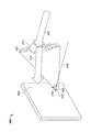
図9は、本明細書に開示の実施例の実装に使用されうる、ロール形成を利用する例示的な形成システムを示している。例示的なロール形成システム900は、溝904を形成するサブ微細構造を備えたローラー902を含む。図9の図解例では、ロール形成システム900は、微細構造(例えば、リブレット)910のリッジ909の上にサブ微細構造(例えば、モスアイサブ微細構造、サブ微細構造リッジなど)908を形成(例えば、エンボス加工)するために使用される。この実施例では、ロール形成システム900は、図8の例示的なロゴマーク800に関連して上に示したように、微細構造910の上に複数のサブ微細構造グループを形成するために使用されうる。
FIG. 9 shows an exemplary formation system utilizing roll formation that can be used to implement the embodiments disclosed herein. An exemplary
ロール形成システム900の動作中、微細構造910は一般的に矢印912によって示された方向に移動し、一方、ローラー902は一般的に矢印914によって示された方向に回転する。この実施例では、リッジ909の上にサブ微細構造908を形成するモスアイ形成構造体は、溝904(例えば、サブ微細構造908を形成するために使用されるツーリング形状及び/又は幾何形状)内にあり、また、リッジ909を受け止める補完的な段形状を有する。溝904の中のモスアイ形成構造体は、例えば、微細構造リッジ909の先端付近により小さなサブ微細構造を形成し、一方で、微細構造リッジ909の別の場所により大きなサブ微細構造を形成するためサイズを変えることができる(図3参照)。幾つかの実施例では、ローラー902を介して微細構造910に適用される力は、微細構造910の上にサブ微細構造908が形成される程度を変えるため、調整される。追加的に又は代替的に、機械加工システム900に対して微細構造910が動くときのライン速度、及び/又はローラー902の回転速度は、微細構造910の上にサブ微細構造908を形成する処理、及び/又は微細構造910の上にサブ微細構造908が形成される程度を制御するために、調整される。幾つかの実施例では、ローラー表面902は、微細構造リッジ909間の微細構造ベース領域918にサブ微細構造(例えば、リッジ)を形成(例えば、エンボス加工)するための構造体916を有しうる。
During the operation of the
図10は、本明細書に開示の実施例の実装に使用されうる、例示的な形成システム1000を示す。例示的な形成システム1000は、整列固定具1004が取り付けられるエンボス加工リグ1002を含む。各固定具1004は、微細構造1010の上にサブ微細構造を形成(例えば、エンボス加工)するため、形成ローラー(例えば、テーパー処理されたエンボス加工ローラー)1006、1008を有する。
FIG. 10 shows an exemplary forming
動作中、図解例の形成システム(例えば、二次処理システム)1000は、微細構造1010が一般的に矢印1012によって示された方向に押し出されるにつれて、微細構造1010の上にサブ微細構造を形成する。この実施例では、微細構造1010は押し出されるリブレット(例えば、リブレット基板)である。エンボス加工リグ1002の動作中、エンボス加工リグ1002は、一般的に両方向矢印1016によって示される上方又は下方に移動しうる。微細構造1010の上にサブ微細構造及び/又はサブ微細構造グループを形成及び/又は付加するため、図解例のローラー1006、1008は、一般的に矢印1020、1022によってそれぞれ示される方向に回転する。
During operation, the illustrated example formation system (eg, secondary processing system) 1000 forms a sub-microstructure on top of the
図11は、図10の例示的な形成システム1000の詳細図である。上述のように、例示的なローラー1006、1008は、微細構造1010の上にサブ微細構造を形成する。ローラー1006、1008が回転し、微細構造1010がローラー1006、1008に対して移動する間に、表面特徴1106は、微細構造1010の上にサブ微細構造1108をエンボス加工するために使用される。特に、表面特徴1106は、微細構造1010の上にサブ微細構造1108をエンボス加工するため、モスアイサブ微細構造及び/又はモスアイ形成構造体又は他の任意の適切なサブ微細構造形成構造体(例えば、リッジ)を含みうる。幾つかの実施例では、ローラー1006、1008を(例えば、上方又は下方、側方に)移動すること、或いは微細構造1010が形成システム1000に対して移動するにつれて微細構造1010に対する圧力を変えることによって、サブ微細構造1108の高さは、微細構造1010の押し出された深さに沿って変化しうる。この実施例では、微細構造1010の各リッジは、寸法1110で示されているように、およそ50〜100ミクロンだけ離されており、各リッジ高は、寸法1112で示されているように、およそ30〜60ミクロンで、また各リッジは、寸法1114で示されているように、ベースでおよそ5〜30ミクロンの幅になっている。この実施例では、微細構造1010の各リッジのピーク間の間隔はおよそ75〜100ミクロンである。前述の寸法及び/又はパラメータは例に過ぎず、用途、ビークルが通過する流体の流体特性及び/又は所定の環境動作条件、などによって変化しうる。
FIG. 11 is a detailed view of the exemplary forming
図12は、1つの微細構造及び/又は複数の微細構造を有する表面の上に、光学的/美的効果、及び/又は画像配置(例えば、画像の表現の配置)を作り出すために使用されうる、サブ微細構造画像システム1200の概略的な表現である。例示的なサブ微細構造画像システム1200は、例示的な画像入力インターフェース1202、例示的なツールコントローラ1204、例示的な画像プロセッサ1206及び例示的なコンパレータ1208を含む。この実施例では、微細構造画像システム1200は、例えば、サブ微細構造及び/又はサブ微細構造の複数のグループのパターンを画定することによって、微細構造上に画像を配置及び/又は画定するために使用される。
FIG. 12 can be used to create an optical / aesthetic effect and / or an image arrangement (eg, an arrangement of an image representation) on a surface having one microstructure and / or a plurality of microstructures. It is a schematic representation of the sub-fine
図解例の画像入力インターフェース1202は、画像及び/又は画像ファイル(例えば、JPEGファイル)を受け取るように使用される。この実施例では、画像プロセッサ1206は、画像入力インターフェース1202から画像及び/又は画像ファイルを受け取り、光学的な効果を作り出す(例えば、微細構造の画像の表現を伝える)ため、サブ微細構造及び/又はサブ微細構造のグループが位置決めされ、形成され、及び/又は形作られる場所をマッピング及び/又は画定する。幾つかの実施例では、画像入力インターフェース1202は、サブ微細構造グループ相互の位置決め及び/又は相対的位置決めを画定しうる。これによって、観測者に認識される深さを作り出す。この実施例では、画像プロセッサ1206は、ツールコントローラ1204に対してマッピング及び/又は画定されたサブ微細構造グループの配置を提供する。これによって、ツールコントローラ1204は、微細構造及び又は複数の微細構造を備えた表面の上に(例えば、サブ微細構造をエンボス加工する、ツールを配向するなど)サブ微細構造を設ける(例えば、重ね合わせる)ように使用され、光学的効果及び/又は観測者によって目視されうる画像を作り出す。
The illustrated
幾つかの実施例では、コンパレータ1208は、例えば、カメラを用いた目視検査によって、ツールコントローラ1204によってもたらされるサブ微細構造を検証する。特に、コンパレータ1208は、例えば、微細構造の検出済み画像に対して、画像入力インターフェース1202に提供された画像を使用することができ、微細構造の上にサブ微細構造を配置することによって、微細構造によって提供される画像の表現を検証する。
In some embodiments, the
図13及び図14には、図12のサブ微細構造画像システム1200の例示的な実装方法が示されているが、図12に示されている一又は複数の要素、処理、及び/又はデバイスは、組み合わされ、分割され、再配置され、省略され、除去され、及び/又は別の方式で実装されてもよい。さらに、図12の例示的な画像入力インターフェース1202、例示的なツールコントローラ1204、例示的な画像プロセッサ1206、例示的なコンパレータ1208、及び/又は、より一般的には、例示的なサブ微細構造画像システム1200は、ハードウェア、ソフトウェア、ファームウェア、及び/又はハードウェア、ソフトウェア、及び/又はファームウェアの任意の組み合わせによって実装されうる。したがって、例えば、図12の例示的な画像入力インターフェース1202、例示的なツールコントローラ1204、例示的な画像プロセッサ1206、例示的なコンパレータ1208のいずれか、及び/又は、より一般的には、例示的なサブ微細構造画像システム1200は、一又は複数のアナログもしくはデジタル回路、ロジック回路、プログラマブルプロセッサ、特定用途向け集積回路(ASIC)、プログラマブルロジックデバイス(PLD)及び/又はフィールドプログラマブルロジックデバイス(FPLD)によって実装されることができる。本特許の装置又はシステムの請求項を、純粋にソフトウェア及び/又はファームウェア実装を包含するものとして読む場合、例示的な画像入力インターフェース1202、例示的なツールコントローラ1204、例示的な画像プロセッサ1206、及び/又は例示的なコンパレータ1208のうちのいずれかは、本明細書において、当該ソフトウェア及び/又はファームウェアを保存するための、メモリ、デジタル多用途ディスク(DVD)、コンパクトディスク(CD)、ブルーレイディスクなどの、有形のコンピュータ可読記憶装置もしくは記憶ディスクを含むよう明示的に定義される。さらに、図12の例示的な微細構造画像システム1200は、図13及び図14に示されるものに加えて、又はこれらの代わりに、一又は複数の要素、処理、及び/もしくはデバイスを含みうる、及び/又は、図示される要素、処理、及びデバイスのいずれかもしくはすべてのものを1つより多く含みうる。
13 and 14 show an exemplary implementation of the
図13及び図14では、図12のサブ微細構造画像システム1200を実装するための例示的方法を表すフロー図が示される。これらの実施例では、方法は、図15との関連で以下に説明される例示的なプロセッサプラットフォーム1500に示すプロセッサ1512などの、プロセッサによる実行のためのプログラムを備える、機械可読命令を使用して実装されうる。プログラムは、CD−ROM、フロッピーディスク、ハードドライブ、デジタル多用途ディスク(DVD)、ブルーレイディスク、又はプロセッサ1512に関連付けられるメモリなどの有形のコンピュータ可読記憶媒体上に記憶されたソフトウェア内に埋め込まれてもよいが、代替的に、プログラムの全体及び/又は部分がプロセッサ1512以外のデバイスによって実行されてもよく、及び/又は、ファームウェアもしくは専用のハードウェアに埋め込まれてもよい。さらに、例示的なプログラムは図13に示すフロー図に関連して記載されているが、例示的なサブ微細構造画像システム1200を実装する他の多くの方法が代替として使用されうる。例えば、ブロックの実行順は変更されることがあり、及び/又は記載されているブロックの幾つかは変更、除外、又は組み合わされることがありうる。
13 and 14 show flow diagrams illustrating an exemplary method for mounting the
上述のように、図13及び図14の例示的な方法は、ハードディスクドライブ、フラッシュメモリ、読取専用メモリ(ROM)、コンパクトディスク(CD)、デジタル多用途ディスク(DVD)、キャッシュ、ランダムアクセスメモリ(RAM)及び/又は、任意の期間にわたって(例えば、長期的に、永続的に、短期的に、一時バッファ用として、及び/又は情報のキャッシング用として)情報が記憶される、任意の他の記憶デバイスもしくは記憶ディスクなど、有形のコンピュータ可読記憶媒体に記憶される符号化された命令(例えば、コンピュータ可読命令及び/又は機械可読命令)を使用して、実装されうる。本明細書で使用されているように、有形のコンピュータ可読記憶媒体という語は、任意のタイプのコンピュータ可読記憶デバイス及び/又は記憶ディスクを含み、伝播信号を除外し、伝送媒体を除外するように明確に定義される。本明細書で使用されているように、「有形のコンピュータ可読記憶媒体」と「有形の機械可読記憶媒体」は、交換可能に使用される。追加的に又は代替的に、図13及び図14の例示的な方法は、ハードディスクドライブ、フラッシュメモリ、読取専用メモリ、コンパクトディスク、デジタル多用途ディスク、キャッシュ、ランダムアクセスメモリ及び/又は、任意の期間にわたって(例えば、長期的に、永続的に、短期的に、一時バッファ用として、及び/又は情報のキャッシング用として)情報が記憶される、任意の他の記憶デバイスもしくは記憶ディスクなど、非一過性コンピュータ可読媒体及び/又は機械可読媒体に記憶される符号化された命令(例えば、コンピュータ可読命令及び/又は機械可読命令)を使用して、実装されうる。本明細書で使用されているように、非一過性コンピュータ可読媒体という語は、任意のタイプのコンピュータ可読記憶デバイス及び/又は記憶ディスクを含み、伝播信号を除外し、伝送媒体を除外するように明確に定義される。本明細書で使用されているように、「少なくとも」という語句は、特許請求項のプリアンブルに記載される移行用語として使用されるが、「含む」という用語がオープンエンド形式であるのと同様にオープンエンド形式である。 As described above, the exemplary methods of FIGS. 13 and 14 include hard disk drives, flash memory, read-only memory (ROM), compact disks (CD), digital versatile disks (DVD), caches, random access memory ( RAM) and / or any other memory in which information is stored over an arbitrary period of time (eg, for long-term, permanent, short-term, temporary buffering, and / or for caching information). It can be implemented using encoded instructions (eg, computer-readable and / or machine-readable) stored in a tangible computer-readable storage medium, such as a device or storage disk. As used herein, the term tangible computer-readable storage medium includes any type of computer-readable storage device and / or storage disk, to exclude propagating signals and to exclude transmission media. Well defined. As used herein, "tangible computer-readable storage media" and "tangible machine-readable storage media" are used interchangeably. Additional or alternative, the exemplary methods of FIGS. 13 and 14 include hard disk drives, flash memory, read-only memory, compact discs, digital versatile disks, caches, random access memory and / or any period of time. Non-transitory, such as any other storage device or storage disk, where information is stored over (eg, long-term, permanent, short-term, for temporary buffering, and / or for caching information). It can be implemented using coded instructions (eg, computer-readable and / or machine-readable) stored on computer-readable and / or machine-readable media. As used herein, the term non-transient computer-readable medium includes any type of computer-readable storage device and / or storage disk to exclude propagating signals and exclude transmission media. Is clearly defined in. As used herein, the phrase "at least" is used as a transitional term as described in the claims preamble, just as the term "contains" is in open-ended form. It is an open-ended format.
図13は、本明細書に開示の実施例の実装に使用されうる、例示的な方法を表わすフロー図である。例示的な方法は、微細構造(例えば、微細構造300、400、600、700、1010)が形成され(例えば、押出成形及び/又は機械加工され)、画像の表現を伝えるパターン(例えば、微細構造の上に重ね合わせられるサブ微細構造のパターン)を画定するため、微細構造の一又は複数の表面の上に重ね合わせられるサブ微細構造及び/又は複数のサブ微細構造グループを受け取るように準備されるブロック1300から始まる。当該画像は人によって認識され、及び/又は図12の画像入力インターフェース1202などの画像入力インターフェースによって受け取られうる(ブロック1300)。
FIG. 13 is a flow diagram illustrating an exemplary method that can be used to implement the embodiments disclosed herein. An exemplary method is a pattern (eg, microstructure) in which microstructures (eg,
ツールは、図12の画像プロセッサ1206などの画像プロセッサからのデータに基づいて微細構造の表面に整列される(ブロック1302)。例えば、シリンダ902などのロール形成シリンダは、図12のツールコントローラ1204などのツールコントローラによって、微細構造(例えば、微細構造906)に整列される。図解例のツールは、視角的手段及び/又は機械的な付勢(例えば、押し出されるにつれて微細構造に負荷をかけるばねなど)によって整列されうる。幾つかの実施例では、微細構造は、ツールに対して正しく整列されるように移動及び/又は位置決めされる。他の実施例では、エンボス加工リグ1002などのエンボス加工リグの機械加工ローラー(例えば、ローラー1006、1008)は、微細構造が押し出されるにつれて(例えば、サブ微細構造を形成するためのインライン二次処理)、視角的手段及び/又は機械的手段によって、微細構造に整列される。
The tools are aligned on the surface of the microstructure based on data from an image processor such as the
次に、ツールは微細構造の上にサブ微細構造の第1グループを設ける(ブロック1304)。この実施例では、サブ微細構造の第1グループはエンボス加工によって微細構造の上に形成される。幾つかの実施例では、微細構造がエンボス加工される及び/又は微細構造の異なる位置にエンボス加工される程度を調整するため、エンボス加工ツールに印加される力は変化する。幾つかの実施例では、微細構造のライン速度及び/又はエンボス加工ローラー(例えば、ローラー902)の回転速度は、例えば、微細構造の異なる位置で微細構造にサブ微細構造が設けられる程度を制御するために変化する。 The tool then provides a first group of sub-microstructures on top of the microstructure (block 1304). In this embodiment, the first group of sub-microstructures is formed on top of the microstructure by embossing. In some embodiments, the force applied to the embossing tool varies in order to adjust the degree to which the microstructure is embossed and / or embossed at different positions in the microstructure. In some embodiments, the line speed of the microstructure and / or the rotational speed of the embossed roller (eg, roller 902) controls, for example, the extent to which the microstructure is provided with sub-microstructures at different positions in the microstructure. Change for.
次に、ツールは別の位置に移動される、及び/又は図12に関連して上述されているツールコントローラ1204などのツールコントローラによって整列(例えば、微細構造の別の部分に整列)される(ブロック1306)。一旦、ツールが再整列及び/又は移動されると、ツールは、微細構造の上にサブ微細構造の第2グループを設けるために使用される(ブロック1308)。代替的に、微細構造の上にサブ微細構造の第2グループを設けるために付加的なツールが使用されうる。幾つかの実施例では、光学的効果を作り出すため、サブ微細構造の第2グループは、サブ微細構造の第1グループとは異なるように整列及び/又は形成されうる。
The tool is then moved to another position and / or aligned (eg, aligned with another part of the microstructure) by a tool controller such as the
次に、付加的なサブ微細構造グループが追加されるかどうかが決定される(ブロック1310)。この決定は、例えば、画像を伝えるため、サブ微細構造を設ける必要性が微細構造にどの程度あるかを判断することによって行われる。特に、コンパレータ1208などのコンパレータは、付加的なサブ微細構造及び又はサブ微細構造グループが追加される必要があるかどうかを判断するため、微細構造の上に表示されるサブ微細構造と、伝えられる画像とを比較するために使用されうる。付加的なサブ微細構造が追加されることになっている場合(ブロック1300)には、処理は反復され、制御はブロック1300に戻る。付加的なサブ微細構造が追加されることになっていない場合(ブロック1310)には、処理は終了する(ブロック1312)。
It is then determined whether additional sub-ultrastructure groups will be added (block 1310). This determination is made, for example, by determining how much the microstructure needs to be provided with a sub-microstructure to convey the image. In particular, a comparator such as
図14は、本明細書に開示の実施例の実装に使用されうる、別の例示的な方法を表わす別のフロー図である。この処理は、画像(例えば、ロゴを表わす画像)が比較的平坦な部分に沿って微細構造を有する表面によって表示されるブロック1400で始まる。最初に、表面に適用される画像は、図12に関連して上述されている画像入力インターフェース1202などの画像インターフェースによって受け取られる(ブロック1404)。次に、サブ微細構造のグループ(例えば、サブ微細構造のパターン)は、画像プロセッサ1206などの画像プロセッサ、及び/又は図12のツールコントローラ1204などのツールコントローラからの命令に基づいて、表面上に及び/又は表面近傍に設けられる。
FIG. 14 is another flow diagram illustrating another exemplary method that may be used to implement the embodiments disclosed herein. This process begins with
サブ微細構造及び/又はサブ微細構造グループは検証される(ブロック1408)。幾つかの実施例では、カメラベースのシステムなどの検査システムは、サブ微細構造及び/又はサブ微細構造グループが微細構造の上に正しく形成されていることを(例えば、目視検証によって)検証する。追加的に又は代替的に、表面の上にサブ微細構造が設けられる(例えば、エンボス加工される)程度が決定及び/又は検証される(例えば、カバーされる微細構造の面積、サブ微細構造の高さ及び/又は高さなど)。 The sub-ultrastructure and / or sub-ultrastructure group is verified (block 1408). In some embodiments, inspection systems, such as camera-based systems, verify (eg, by visual verification) that the sub-ultrastructure and / or sub-ultrastructure groups are correctly formed on the microstructure. Additional or alternative, the extent to which the sub-microstructure is provided (eg, embossed) on the surface is determined and / or verified (eg, the area of the microstructure covered, the sub-microstructure Height and / or height, etc.).
次に、付加的な画像又は画像の一部が表面に設けられるべきかどうかが決定される(ブロック1410)。この決定は、例えば、画像を伝えるため、サブ微細構造を設ける必要性が微細構造にどの程度あるかを判断することによって行われる。特に、コンパレータ1208などのコンパレータは、付加的な画像が表面に追加される必要があるかどうかを判断するために、表示されているサブ微細構造と画像とを比較するため使用されうる。付加的な画像又は画像の一部が表面に追加されるべきである場合(ブロック1410)には、処理は反復され、制御はブロック1400に戻る。付加的な画像が追加されることになっていない場合(ブロック1410)には、処理は終了する(ブロック1412)。
It is then determined whether an additional image or part of the image should be provided on the surface (block 1410). This determination is made, for example, by determining how much the microstructure needs to be provided with a sub-microstructure to convey the image. In particular, a comparator such as
図15は、図12のサブ微細構造画像システム1200を実装するため、図13及び図14の方法を実装するための命令を実行することができる、例示的なプロセッサプラットフォーム1500のブロック図である。プロセッサプラットフォーム1500は、例えば、サーバ、パーソナルコンピュータ、モバイルデバイス(例えば、携帯電話、スマートフォン、iPad(商標)などのタブレット)、パーソナルデジタルアシスタント(PDA)、インターネット家電、デジタルビデオレコーダ、セットトップボックス、又は他の任意のコンピューティングデバイスであってもよい。
FIG. 15 is a block diagram of an
図解例のプロセッサプラットフォーム1500は、プロセッサ1512を含む。図解例のプロセッサ1512は、ハードウェアである。例えば、プロセッサ1512は、任意の望ましい系列会社もしくは製造者からの一又は複数の集積回路、論理回路、マイクロプロセッサ、又はコントローラによって実装されることができる。
The illustrated
図解例のプロセッサ1512は、ローカルメモリ1513(例えば、キャッシュ)を含む。この実施例では、プロセッサ1512はまた、画像入力インターフェース1202、ツールコントローラ1204、画像プロセッサ1206及びコンパレータ1208を含む。図解例のプロセッサ1512は、揮発性メモリ1514及び不揮発性メモリ1516を含むメインメモリと、バス1518を介して通信可能である。揮発性メモリ1514は、同期型ダイナミックランダムアクセスメモリ(SDRAM)、ダイナミックランダムアクセスメモリ(DRAM)、RAMBUSダイナミックランダムアクセスメモリ(RDRAM)、及び/又は任意の他のタイプのランダムアクセスメモリデバイスによって実装されうる。不揮発性メモリ1516は、フラッシュメモリ及び/又は任意の望ましいタイプのメモリデバイスによって実装されうる。メインメモリ1514、1516へのアクセスは、メモリコントローラによって制御される。
The illustrated
図解例のプロセッサプラットフォーム1500は、インターフェース回路1520も含む。インターフェース回路1520は、イーサネットインターフェース、ユニバーサルシリアルバス(USB)、及び/又はPCIエクスプレスインターフェースといった任意のタイプのインターフェース規格で実装されうる。
The illustrated
図解例では、一又は複数の入力デバイス1522がインターフェース回路1520に接続される。入力デバイス1522は、ユーザがデータ及びコマンドをプロセッサ1512に入力することを可能にする。入力デバイスは、例えば、音声センサ、マイクロフォン、カメラ(静止画又はビデオ)、キーボード、ボタン、マウス、タッチスクリーン、トラックパッド、トラックボール、アイソポイント(isopoint)、及び/又は音声認識システムによって実装されることができる。
In the illustrated example, one or
一又は複数の出力デバイス1524も、図解例のインターフェース回路1520に接続される。出力デバイス1524は、例えば、ディスプレイデバイス(例えば、発光ダイオード(LED)、有機発光ダイオード(OLED)、液晶ディスプレイ、タッチスクリーン、触覚出力デバイス、プリンタ及び/又はスピーカ)によって、実装されうる。したがって、図解例のインターフェース回路1520は、典型的にはグラフィックドライバカード、グラフィックドライバチップ又はグラフィックドライバプロセッサを含む。
One or
図解例のインターフェース回路1520は、外部の機械(例えば、任意の種類のコンピューティングデバイス)との、ネットワーク1526(例えば、イーサネット接続、デジタル加入者線(DSL)、電話線、同軸ケーブル、セルラフォンシステムなど)を介したデータ交換を容易にするための、送信機、受信機、トランシーバ、モデム、及び/又はネットワークインターフェースカードなどの通信デバイスも含む。
The illustrated
図解例のプロセッサプラットフォーム1500は、ソフトウェア及び/又はデータを記憶するための一又は複数の大容量記憶デバイス1528も含む。そのような大容量記憶デバイス1528は、フロッピーディスク、ハードドライブディスク、コンパクトディスク、ブルーレイディスク、RAIDシステム、及びデジタル多用途ディスク(DVD)ドライブを含む。
The illustrated
図13及び図14の方法を実装するための符号化された命令1532は、大容量記憶デバイス1528、揮発性メモリ1514、不揮発性メモリ1516、及び/又はCD若しくはDVDなどの取り外し可能な有形のコンピュータ可読記憶媒体に、記憶されうる。
Encoded
本明細書では特定の例示的な方法、装置、及び製品が開示されるが、本特許出願の範囲はこれらに限定されるものではない。反対に、本特許出願は、本特許出願の特許請求の範囲内に公正に当てはまるすべての方法、装置、及び製品を包含する。航空機が記載されているが、例示的な方法及び装置は、他のビークル、船舶、空気力学的構造などに適用されうる。 Although specific exemplary methods, devices, and products are disclosed herein, the scope of this patent application is not limited thereto. On the contrary, the patent application includes all methods, devices, and products that are fairly applicable within the claims of the patent application. Aircraft are described, but exemplary methods and devices can be applied to other vehicles, ships, aerodynamic structures, and the like.
Claims (12)
前記微細構造によって引き起こされる反射、及び/又は反射率の変化を制御して、グラフィックの表現を伝えるために前記微細構造の上に重ね合わせられたサブ微細構造のパターンと
を備え、サブ微細構造の前記パターンは、第1の反射特性を有するサブ微細構造の第1グループと、前記第1の反射特性とは異なる第2の反射特性を有するサブ微細構造の第2グループとを備え、
サブ微細構造の前記第2グループは、サブ微細構造の前記第1グループと比較して、異なる形状、又は配向を有する装置。 With the aerodynamic microstructure that defines the outer surface of the vehicle
Reflections caused by the previous SL microstructure, and / or by controlling the change in reflectivity, a pattern of sub-microstructure superimposed on said microstructure to convey graphical representation, sub-microstructure The pattern includes a first group of sub-microstructures having a first reflection characteristic and a second group of sub-microstructures having a second reflection characteristic different from the first reflection characteristics.
The second group of the sub-microstructure is an apparatus having a different shape or orientation as compared with the first group of the sub-microstructure.
前記外部表面上又は前記外部表面近傍に前記第1の反射特性とは異なる第2の反射特性を有するサブ微細構造の第2グループを設けること
を含む方法であって、前記微細構造によって引き起こされる反射、及び/又は反射率の変化を制御して、光学的な効果を作り出すために、サブ微細構造の前記第2グループは、サブ微細構造の前記第1グループと比較して、異なる形状、又は配向を有する、方法。 Providing a first group of sub-microstructures with a first reflective property on the outer surface of the microstructure.
Wherein there is provided a method comprising providing a second group of sub-microscopic structures having different second reflection characteristic from said first reflection characteristic on or in the external surface near the outer surface, caused by the previous SL microstructure In order to control reflections and / or changes in reflectance to create an optical effect, the second group of sub-ultrastructures may have a different shape or shape as compared to the first group of sub-ultrastructures. A method with orientation.
Applications Claiming Priority (2)
| Application Number | Priority Date | Filing Date | Title |
|---|---|---|---|
| US14/705,547 | 2015-05-06 | ||
| US14/705,547 US9751618B2 (en) | 2015-05-06 | 2015-05-06 | Optical effects for aerodynamic microstructures |
Publications (3)
| Publication Number | Publication Date |
|---|---|
| JP2017019484A JP2017019484A (en) | 2017-01-26 |
| JP2017019484A5 JP2017019484A5 (en) | 2019-05-30 |
| JP6854088B2 true JP6854088B2 (en) | 2021-04-07 |
Family
ID=55854646
Family Applications (1)
| Application Number | Title | Priority Date | Filing Date |
|---|---|---|---|
| JP2016080285A Active JP6854088B2 (en) | 2015-05-06 | 2016-04-13 | Optical effects of aerodynamic ultrastructure |
Country Status (7)
| Country | Link |
|---|---|
| US (1) | US9751618B2 (en) |
| EP (1) | EP3103717B1 (en) |
| JP (1) | JP6854088B2 (en) |
| KR (1) | KR102481656B1 (en) |
| CN (1) | CN106126768B (en) |
| AU (1) | AU2016201149B2 (en) |
| BR (1) | BR102016007446B1 (en) |
Families Citing this family (16)
| Publication number | Priority date | Publication date | Assignee | Title |
|---|---|---|---|---|
| US9868135B2 (en) | 2015-05-06 | 2018-01-16 | The Boeing Company | Aerodynamic microstructures having sub-microstructures |
| US9714083B2 (en) | 2015-05-06 | 2017-07-25 | The Boeing Company | Color applications for aerodynamic microstructures |
| KR101813341B1 (en) * | 2015-12-28 | 2017-12-28 | 삼성전기주식회사 | Manufacturing Method of Magnetic sheet and Roller Therefore |
| US10105877B2 (en) | 2016-07-08 | 2018-10-23 | The Boeing Company | Multilayer riblet applique and methods of producing the same |
| ES2900244T3 (en) * | 2017-05-05 | 2022-03-16 | 3M Innovative Properties Co | profiled films |
| JP6904208B2 (en) * | 2017-10-10 | 2021-07-14 | トヨタ自動車株式会社 | Axis misalignment judgment device |
| US11960107B2 (en) | 2018-01-17 | 2024-04-16 | Nanotech Security Corp. | Nano-structures patterned on micro-structures |
| US12065236B2 (en) * | 2020-01-23 | 2024-08-20 | Enterprise Science Fund, Llc | Systems and methods for active control of surface drag using intermittent or variable actuation |
| US11905983B2 (en) | 2020-01-23 | 2024-02-20 | Deep Science, Llc | Systems and methods for active control of surface drag using electrodes |
| CN112124561B (en) * | 2020-09-27 | 2022-02-25 | 中国商用飞机有限责任公司 | Aerodynamic drag reduction structure for wingtip winglet of aircraft and aircraft |
| US11618511B2 (en) | 2021-01-12 | 2023-04-04 | Honda Motor Co., Ltd. | Surface pattern for a vehicle |
| US11466709B2 (en) | 2021-02-17 | 2022-10-11 | Deep Science, Llc | In-plane transverse momentum injection to disrupt large-scale eddies in a turbulent boundary layer |
| US20240191986A1 (en) | 2021-04-20 | 2024-06-13 | Nikon Corporation | Systems and methods for measuring height properties of surfaces |
| US20220410246A1 (en) * | 2021-06-25 | 2022-12-29 | Ultracell Llc | Fuselage heat exchanger for cooling power source for unmanned aerial vehicles (uavs) |
| US11987021B2 (en) | 2021-09-01 | 2024-05-21 | The Boeing Company | Multilayer riblet appliques |
| JPWO2023127152A1 (en) | 2021-12-28 | 2023-07-06 |
Family Cites Families (98)
| Publication number | Priority date | Publication date | Assignee | Title |
|---|---|---|---|---|
| US4706910A (en) | 1984-12-27 | 1987-11-17 | The United States Of America As Represented By The Administrator Of The National Aeronautics And Space Administration | Combined riblet and lebu drag reduction system |
| US5133516A (en) * | 1985-05-31 | 1992-07-28 | Minnesota Mining And Manufacturing Co. | Drag reduction article |
| US4986496A (en) * | 1985-05-31 | 1991-01-22 | Minnesota Mining And Manufacturing | Drag reduction article |
| DE3522943A1 (en) | 1985-06-27 | 1987-01-08 | Messerschmitt Boelkow Blohm | DEVICE FOR REDUCING TURBULENT FRICTION RESISTANCE IN AIR, SPACE AND WATER VEHICLES |
| US4650138A (en) | 1985-09-30 | 1987-03-17 | Internorth, Inc. | Cascaded micro-groove aerodynamic drag reducer |
| US4932612A (en) | 1986-02-25 | 1990-06-12 | Blackwelder Ron F | Method and apparatus for reducing turbulent skin friction |
| GB8706554D0 (en) | 1987-03-19 | 1987-04-23 | Rolls Royce Plc | Boundary layer devices |
| US4930729A (en) | 1986-05-22 | 1990-06-05 | Rolls-Royce Plc | Control of fluid flow |
| US5133519A (en) | 1989-04-21 | 1992-07-28 | Board Of Trustees Operating Michigan State University | Drag reduction method and surface |
| US5054412A (en) | 1989-10-31 | 1991-10-08 | The United States Of America As Represented By The Administrator Of The National Aeronautics And Space Administration | Hydrodynamic skin-friction reduction |
| US5445095A (en) | 1990-08-14 | 1995-08-29 | The United States Of America As Represented By The Administrator Of The National Aeronautics And Space Administration | Polymer/riblet combination for hydrodynamic skin friction reduction |
| DE9316009U1 (en) | 1993-10-20 | 1994-01-13 | Moser, Josef, 85435 Erding | Surface of a fluid-flowed body |
| US5505543A (en) | 1994-01-21 | 1996-04-09 | The Boeing Company | Emissivity measurement apparatus and method |
| US5637873A (en) | 1995-06-07 | 1997-06-10 | The Boeing Company | Directional reflectometer for measuring optical bidirectional reflectance |
| US5520717A (en) | 1995-06-07 | 1996-05-28 | The Boeing Company | Isolating nanophase amorphous magnetic metals |
| US6982794B1 (en) | 1995-06-07 | 2006-01-03 | The Boeing Company | Directional reflectometer |
| US5766306A (en) | 1996-06-04 | 1998-06-16 | The Boeing Company | Continuous process for making nanoscale amorphous magnetic metals |
| US5766764A (en) | 1996-06-04 | 1998-06-16 | The Boeing Company | Nanoscale amorphous magnetic metals |
| DE19650439C1 (en) | 1996-12-05 | 1998-03-12 | Deutsch Zentr Luft & Raumfahrt | Ribbed surface for wall subjected to turbulent airflow |
| US6191248B1 (en) | 1996-12-19 | 2001-02-20 | The Boeing Company | Coating |
| US5874167A (en) | 1996-12-19 | 1999-02-23 | The Boeing Company | High efficiency metal pigments |
| CA2272602A1 (en) | 1996-12-20 | 1998-07-02 | Diane C. Rawlings | Appliques providing corrosion protection |
| US6376063B1 (en) | 1998-06-15 | 2002-04-23 | The Boeing Company | Making particulates of controlled dimensions by electroplating |
| US6475616B1 (en) | 1999-11-30 | 2002-11-05 | 3M Innovative Properties Company | Paint replacement appliques |
| US6345791B1 (en) * | 2000-04-13 | 2002-02-12 | Lockheed Martin Corporation | Streamwise variable height riblets for reducing skin friction drag of surfaces |
| GB0108740D0 (en) | 2001-04-06 | 2001-05-30 | Bae Systems Plc | Turbulent flow drag reduction |
| EP1404508A1 (en) | 2001-06-21 | 2004-04-07 | Bernd Späth | Body with improved surface properties |
| PL204021B1 (en) * | 2001-11-02 | 2009-12-31 | Cnt Spo & Lstrok Ka Z Ogranicz | Superhydrophobous coating |
| US7703179B2 (en) | 2001-11-09 | 2010-04-27 | 3M Innovative Properties Company | Microreplicated surface |
| DE10217111A1 (en) | 2002-04-17 | 2003-11-06 | Roehm Gmbh | Solid with microstructured surface |
| US7044073B2 (en) | 2002-04-26 | 2006-05-16 | Board Of Regents Of The University Of Texas System | Methods for reducing the viscous drag on a surface and drag reducing device |
| GB0213551D0 (en) | 2002-06-13 | 2002-07-24 | Univ Nottingham | Controlling boundary layer fluid flow |
| US6958207B1 (en) * | 2002-12-07 | 2005-10-25 | Niyaz Khusnatdinov | Method for producing large area antireflective microtextured surfaces |
| KR20040061658A (en) | 2002-12-31 | 2004-07-07 | 삼성전자주식회사 | Hybrid achromatic optical lens and manufacturing method thereof |
| US7070850B2 (en) | 2002-12-31 | 2006-07-04 | 3M Innovative Properties Company | Drag reduction article and method of use |
| US7224529B2 (en) | 2003-09-09 | 2007-05-29 | 3M Innovative Properties Company | Microreplicated article |
| US7867621B2 (en) | 2003-09-30 | 2011-01-11 | The Boeing Company | Wide area lightning diverter overlay |
| CA2538808C (en) | 2003-09-30 | 2011-04-19 | The Boeing Company | Applique |
| DE10346124B4 (en) | 2003-10-01 | 2005-12-01 | Fraunhofer-Gesellschaft zur Förderung der angewandten Forschung e.V. | Tool and method for producing a microstructured surface and use of a tool and the object produced therewith |
| US7252869B2 (en) * | 2003-10-30 | 2007-08-07 | Niyaz Khusnatdinov | Microtextured antireflective surfaces with reduced diffraction intensity |
| US7510149B2 (en) | 2004-08-02 | 2009-03-31 | Lockheed Martin Corporation | System and method to control flowfield vortices with micro-jet arrays |
| US20070060026A1 (en) | 2005-09-09 | 2007-03-15 | Chien-Min Sung | Methods of bonding superabrasive particles in an organic matrix |
| ATE500001T1 (en) | 2005-03-09 | 2011-03-15 | 3M Innovative Properties Co | MICRREPLICATED ARTICLE AND METHOD OF PRODUCTION THEREOF |
| KR20070111544A (en) | 2005-03-09 | 2007-11-21 | 쓰리엠 이노베이티브 프로퍼티즈 컴파니 | Apparatus and method for making microreplicated article |
| US20080233356A1 (en) | 2005-09-12 | 2008-09-25 | Perlen Converting Ag | Method for the Application of a Structured Coating Upon a Smooth Surface |
| US7544407B1 (en) | 2005-09-17 | 2009-06-09 | The Boeing Company | Pressure sensitive adhesive suitable for aircraft exterior applications |
| US7757591B2 (en) * | 2005-10-19 | 2010-07-20 | 3M Innovative Properties Company | Aligned multi-diamond cutting tool assembly for creating microreplication tools |
| US7445409B2 (en) * | 2005-10-19 | 2008-11-04 | 3M Innovative Properties Company | Cutting tool assembly including diamond cutting tips at half-pitch spacing for land feature creation |
| US7755670B2 (en) | 2005-10-24 | 2010-07-13 | Nikon Corporation | Tone-conversion device for image, program, electronic camera, and tone-conversion method |
| US8292226B2 (en) | 2005-11-15 | 2012-10-23 | The Boeing Company | Weight-optimizing internally pressurized composite-body aircraft fuselages having near-elliptical cross sections |
| US8113469B2 (en) * | 2006-02-21 | 2012-02-14 | University Of Alabama | Passive micro-roughness array for drag modification |
| EP1855127A1 (en) * | 2006-05-12 | 2007-11-14 | Rolic AG | Optically effective surface relief microstructures and method of making them |
| US10611468B2 (en) | 2006-09-08 | 2020-04-07 | Steven Sullivan | Method and apparatus for mitigating trailing vortex wakes of lifting or thrust generating bodies |
| US7525785B2 (en) | 2006-12-14 | 2009-04-28 | The Boeing Company | Lightning strike protection method and apparatus |
| US7864501B2 (en) | 2006-12-14 | 2011-01-04 | The Boeing Company | Electrical connects for charge distribution applique |
| US7678997B2 (en) | 2006-12-19 | 2010-03-16 | The Boeing Company | Large area circuitry using appliqués |
| WO2008121418A1 (en) * | 2007-03-30 | 2008-10-09 | The University Of Alabama | A passive drag modification system |
| US7940462B2 (en) * | 2007-08-28 | 2011-05-10 | Nissan Motor Co., Ltd. | Antireflective structure and antireflective molded body |
| US20130062004A1 (en) | 2007-12-12 | 2013-03-14 | The Boeing Company | Aerodynamic surfaces having drag-reducing riblets and method of fabricating the same |
| US20140023837A1 (en) | 2007-12-13 | 2014-01-23 | The Boeing Company | Aircraft structures bonded with adhesive including magnetostrictive material |
| US8343298B2 (en) | 2007-12-13 | 2013-01-01 | The Boeing Company | Aircraft structures bonded with adhesive including magnetostrictive material |
| US8286909B2 (en) | 2008-02-08 | 2012-10-16 | Stratocomm Corporation | Boundary layer propulsion airship with related system and method |
| FI20080248L (en) * | 2008-03-28 | 2009-09-29 | Savcor Face Group Oy | Chemical gas coating and method for forming gas coating |
| CA2731833A1 (en) | 2008-08-05 | 2010-02-11 | Alcoa Inc. | Metal sheets and plates having friction-reducing textured surfaces and methods of manufacturing same |
| DE102008042237B4 (en) | 2008-09-19 | 2010-07-15 | Airbus Deutschland Gmbh | Metallic coating |
| US20110274875A1 (en) | 2008-11-21 | 2011-11-10 | The University Of Alabama | Passive drag modification system |
| US8668166B2 (en) | 2009-01-29 | 2014-03-11 | The Boeing Company | Shape memory riblets |
| US8684310B2 (en) | 2009-01-29 | 2014-04-01 | The Boeing Company | Rigid tipped riblets |
| US9352533B2 (en) | 2009-01-29 | 2016-05-31 | The Boeing Company | Elastomeric riblets |
| US8678316B2 (en) | 2009-01-29 | 2014-03-25 | The Boeing Company | Amorphous metal riblets |
| US8220754B2 (en) | 2009-06-03 | 2012-07-17 | Lockheed Martin Corporation | Plasma enhanced riblet |
| US20110006165A1 (en) | 2009-07-10 | 2011-01-13 | Peter Ireland | Application of conformal sub boundary layer vortex generators to a foil or aero/ hydrodynamic surface |
| US8413928B2 (en) * | 2009-09-25 | 2013-04-09 | The Boeing Company | Structurally designed aerodynamic riblets |
| US8733702B1 (en) * | 2009-12-02 | 2014-05-27 | The Boeing Company | Reduced solar absorptivity applique |
| US20130028744A1 (en) | 2010-01-14 | 2013-01-31 | Pontus Nordin | Aerodynamic surface with improved properties |
| US20110186685A1 (en) | 2010-02-02 | 2011-08-04 | The Boeing Company | Thin-Film Composite Having Drag-Reducing Riblets and Method of Making the Same |
| DE102010031227A1 (en) | 2010-07-12 | 2012-01-12 | Fraunhofer-Gesellschaft zur Förderung der angewandten Forschung e.V. | Device for testing microstructuring quality |
| GB201012737D0 (en) | 2010-07-29 | 2010-09-15 | Airbus Operations Ltd | Improvements to aircraft refuel system piping |
| EP2799150B1 (en) | 2013-05-02 | 2016-04-27 | Hexagon Technology Center GmbH | Graphical application system |
| US8460779B2 (en) * | 2011-03-30 | 2013-06-11 | General Electric Company | Microstructures for reducing noise of a fluid dynamic structure |
| DE102011106763A1 (en) | 2011-07-05 | 2013-01-10 | Eads Deutschland Gmbh | A method of manufacturing a surface of a reduced airflow resistance component and a reduced airflow resistance component |
| DE102011114832A1 (en) | 2011-10-05 | 2013-04-11 | Eads Deutschland Gmbh | RIBBON FILM AND METHOD FOR THE PRODUCTION THEREOF |
| WO2013134657A1 (en) | 2012-03-08 | 2013-09-12 | The University Of Alabama | A passive drag modification system |
| US8875511B2 (en) | 2012-03-30 | 2014-11-04 | Larry C. Simpson | Geothermal wind system |
| FI20126040L (en) | 2012-10-05 | 2014-04-06 | Iscent Oy | Process for the production of micro- or nanostructures in polymer film material |
| US10011916B2 (en) | 2012-10-19 | 2018-07-03 | Ut-Battelle, Llc | Superhydrophobic anodized metals and method of making same |
| US20140116597A1 (en) | 2012-11-01 | 2014-05-01 | The Boeing Company | Methods and apparatus for heating a material |
| US20140238646A1 (en) | 2013-02-25 | 2014-08-28 | Alcatel-Lucent Ireland Ltd. | Sloped hierarchically-structured surface designs for enhanced condensation heat transfer |
| DE102013102164A1 (en) | 2013-03-05 | 2014-09-11 | Airbus Operations Gmbh | A method of coating a surface of an aircraft and an aircraft coated therewith |
| US20140272237A1 (en) | 2013-03-15 | 2014-09-18 | Prc-Desoto International, Inc. | Strippable film assembly and coating for drag reduction |
| US20140363637A1 (en) | 2013-06-06 | 2014-12-11 | The Boeing Company | Heating Layer for Film Removal |
| DE102013013817A1 (en) | 2013-08-22 | 2015-02-26 | Airbus Defence and Space GmbH | Structural component with a riblet surface |
| US9994301B2 (en) | 2013-11-18 | 2018-06-12 | Rohr, Inc. | Virtual aerodynamic surface systems |
| US20160243586A1 (en) | 2014-08-01 | 2016-08-25 | The Boeing Company | Drag reduction riblets integrated in a paint layer |
| US10059435B2 (en) | 2014-12-04 | 2018-08-28 | Parker-Hannifin Corporation | Low drag skin heat exchanger |
| FR3029813B1 (en) | 2014-12-16 | 2019-07-19 | Airbus Operations (S.A.S.) | METHOD FOR MANUFACTURING MICROSTRUCTURE COATING |
| US9868135B2 (en) | 2015-05-06 | 2018-01-16 | The Boeing Company | Aerodynamic microstructures having sub-microstructures |
| US9714083B2 (en) | 2015-05-06 | 2017-07-25 | The Boeing Company | Color applications for aerodynamic microstructures |
-
2015
- 2015-05-06 US US14/705,547 patent/US9751618B2/en active Active
-
2016
- 2016-02-24 AU AU2016201149A patent/AU2016201149B2/en active Active
- 2016-03-04 KR KR1020160026139A patent/KR102481656B1/en active IP Right Grant
- 2016-04-04 BR BR102016007446-0A patent/BR102016007446B1/en active IP Right Grant
- 2016-04-13 JP JP2016080285A patent/JP6854088B2/en active Active
- 2016-04-26 EP EP16167099.7A patent/EP3103717B1/en active Active
- 2016-05-06 CN CN201610297321.1A patent/CN106126768B/en active Active
Also Published As
| Publication number | Publication date |
|---|---|
| JP2017019484A (en) | 2017-01-26 |
| AU2016201149A1 (en) | 2016-11-24 |
| CN106126768B (en) | 2021-11-02 |
| KR20160131869A (en) | 2016-11-16 |
| EP3103717A1 (en) | 2016-12-14 |
| BR102016007446B1 (en) | 2022-06-14 |
| KR102481656B1 (en) | 2022-12-26 |
| US9751618B2 (en) | 2017-09-05 |
| CN106126768A (en) | 2016-11-16 |
| BR102016007446A2 (en) | 2017-01-24 |
| US20160325823A1 (en) | 2016-11-10 |
| AU2016201149B2 (en) | 2020-03-12 |
| EP3103717B1 (en) | 2020-06-03 |
Similar Documents
| Publication | Publication Date | Title |
|---|---|---|
| JP6854088B2 (en) | Optical effects of aerodynamic ultrastructure | |
| JP6854089B2 (en) | Aerodynamic ultrastructure with sub-ultrastructure | |
| EP3103647B1 (en) | Color applications for aerodynamic microstructures | |
| JP2017019484A5 (en) | ||
| US9524416B1 (en) | Fingerprint sensing device comprising three-dimensional pattern | |
| US20140009836A1 (en) | Wood-like films and other decorative films utilizing fresnel mirrors | |
| US10335996B2 (en) | Using depth in three-dimensional object printing to form colors that change with viewing and illumination angles | |
| WO2018077712A1 (en) | Method for 3d printing a 3d item with a decorative surface texture | |
| JPWO2016006651A1 (en) | Optical member and manufacturing method thereof | |
| Ji et al. | Lenticular‐Lens‐Based Colored Antiglare Dashboard Surfaces | |
| BR102016007305A2 (en) | APPARATUS, AND, METHOD | |
| Pagliano | Geometries of Anamorphic Transcriptions | |
| TWI767555B (en) | Cover plate structure and manufacturing method thereof | |
| CN208937734U (en) | Retroreflecting film with the anti-pseudocurve of continous way |
Legal Events
| Date | Code | Title | Description |
|---|---|---|---|
| A521 | Request for written amendment filed |
Free format text: JAPANESE INTERMEDIATE CODE: A523 Effective date: 20190415 |
|
| A621 | Written request for application examination |
Free format text: JAPANESE INTERMEDIATE CODE: A621 Effective date: 20190415 |
|
| A131 | Notification of reasons for refusal |
Free format text: JAPANESE INTERMEDIATE CODE: A131 Effective date: 20200630 |
|
| A521 | Request for written amendment filed |
Free format text: JAPANESE INTERMEDIATE CODE: A523 Effective date: 20200929 |
|
| TRDD | Decision of grant or rejection written | ||
| A01 | Written decision to grant a patent or to grant a registration (utility model) |
Free format text: JAPANESE INTERMEDIATE CODE: A01 Effective date: 20210309 |
|
| A61 | First payment of annual fees (during grant procedure) |
Free format text: JAPANESE INTERMEDIATE CODE: A61 Effective date: 20210315 |
|
| R150 | Certificate of patent or registration of utility model |
Ref document number: 6854088 Country of ref document: JP Free format text: JAPANESE INTERMEDIATE CODE: R150 |
|
| R250 | Receipt of annual fees |
Free format text: JAPANESE INTERMEDIATE CODE: R250 |