JP6830214B2 - Power converter - Google Patents
Power converter Download PDFInfo
- Publication number
- JP6830214B2 JP6830214B2 JP2019225629A JP2019225629A JP6830214B2 JP 6830214 B2 JP6830214 B2 JP 6830214B2 JP 2019225629 A JP2019225629 A JP 2019225629A JP 2019225629 A JP2019225629 A JP 2019225629A JP 6830214 B2 JP6830214 B2 JP 6830214B2
- Authority
- JP
- Japan
- Prior art keywords
- capacitor
- substrate
- switch element
- phase
- bus bar
- Prior art date
- Legal status (The legal status is an assumption and is not a legal conclusion. Google has not performed a legal analysis and makes no representation as to the accuracy of the status listed.)
- Active
Links
- 239000003990 capacitor Substances 0.000 claims description 578
- 239000000758 substrate Substances 0.000 claims description 253
- 239000003985 ceramic capacitor Substances 0.000 claims description 79
- 238000006243 chemical reaction Methods 0.000 claims description 47
- 229910052751 metal Inorganic materials 0.000 claims description 18
- 239000002184 metal Substances 0.000 claims description 18
- 230000005540 biological transmission Effects 0.000 claims description 17
- 238000005476 soldering Methods 0.000 claims description 11
- 239000000463 material Substances 0.000 claims description 10
- 230000002093 peripheral effect Effects 0.000 claims description 6
- 230000003071 parasitic effect Effects 0.000 description 33
- 230000004048 modification Effects 0.000 description 32
- 238000012986 modification Methods 0.000 description 32
- 238000010438 heat treatment Methods 0.000 description 27
- 238000009499 grossing Methods 0.000 description 22
- 238000010586 diagram Methods 0.000 description 9
- 230000005856 abnormality Effects 0.000 description 8
- 230000001629 suppression Effects 0.000 description 8
- 238000010521 absorption reaction Methods 0.000 description 7
- 229910000679 solder Inorganic materials 0.000 description 7
- 230000002159 abnormal effect Effects 0.000 description 5
- 230000006870 function Effects 0.000 description 4
- 230000036544 posture Effects 0.000 description 4
- 239000004020 conductor Substances 0.000 description 3
- 230000000694 effects Effects 0.000 description 3
- 238000009434 installation Methods 0.000 description 3
- 230000001172 regenerating effect Effects 0.000 description 3
- 238000003466 welding Methods 0.000 description 3
- XEEYBQQBJWHFJM-UHFFFAOYSA-N Iron Chemical compound [Fe] XEEYBQQBJWHFJM-UHFFFAOYSA-N 0.000 description 2
- 229910052782 aluminium Inorganic materials 0.000 description 2
- XAGFODPZIPBFFR-UHFFFAOYSA-N aluminium Chemical compound [Al] XAGFODPZIPBFFR-UHFFFAOYSA-N 0.000 description 2
- 239000002131 composite material Substances 0.000 description 2
- 229920001940 conductive polymer Polymers 0.000 description 2
- 238000009413 insulation Methods 0.000 description 2
- 238000000465 moulding Methods 0.000 description 2
- 238000010397 one-hybrid screening Methods 0.000 description 2
- 230000008929 regeneration Effects 0.000 description 2
- 238000011069 regeneration method Methods 0.000 description 2
- 239000004065 semiconductor Substances 0.000 description 2
- 230000001360 synchronised effect Effects 0.000 description 2
- 238000010396 two-hybrid screening Methods 0.000 description 2
- 229910001369 Brass Inorganic materials 0.000 description 1
- RYGMFSIKBFXOCR-UHFFFAOYSA-N Copper Chemical compound [Cu] RYGMFSIKBFXOCR-UHFFFAOYSA-N 0.000 description 1
- HBBGRARXTFLTSG-UHFFFAOYSA-N Lithium ion Chemical compound [Li+] HBBGRARXTFLTSG-UHFFFAOYSA-N 0.000 description 1
- 230000003044 adaptive effect Effects 0.000 description 1
- 229910045601 alloy Inorganic materials 0.000 description 1
- 239000000956 alloy Substances 0.000 description 1
- 239000010951 brass Substances 0.000 description 1
- 229910052802 copper Inorganic materials 0.000 description 1
- 239000010949 copper Substances 0.000 description 1
- 238000005520 cutting process Methods 0.000 description 1
- 239000003792 electrolyte Substances 0.000 description 1
- 239000008151 electrolyte solution Substances 0.000 description 1
- 230000005669 field effect Effects 0.000 description 1
- 230000014509 gene expression Effects 0.000 description 1
- 229910052742 iron Inorganic materials 0.000 description 1
- 229910001416 lithium ion Inorganic materials 0.000 description 1
- 238000004519 manufacturing process Methods 0.000 description 1
- 239000011347 resin Substances 0.000 description 1
- 229920005989 resin Polymers 0.000 description 1
- 238000010399 three-hybrid screening Methods 0.000 description 1
- XLYOFNOQVPJJNP-UHFFFAOYSA-N water Substances O XLYOFNOQVPJJNP-UHFFFAOYSA-N 0.000 description 1
- 238000004804 winding Methods 0.000 description 1
Images


Description
この開示は、電力変換装置に関する。 This disclosure relates to a power converter.
例えば、特許文献1に開示される電力変換装置は、交流をスイッチ素子で直流に変換するコンバータ部と、コンバータ部で変換した直流を平滑する平滑コンデンサ部と、平滑した直流をスイッチ素子で交流に変換するインバータ部とを有している。平滑コンデンサ部は、コンバータ側平滑コンデンサと、インバータ側平滑コンデンサと、コンバータ側コンデンサとインバータ側コンデンサに挟まれた中央側平滑コンデンサから構成されている。中央側平滑コンデンサは電解コンデンサであり、コンバータ側平滑コンデンサとインバータ側平滑コンデンサは、フィルムコンデンサ或いはセラミックコンデンサである。つまり、平滑コンデンサ部は、二種類のコンデンサを有している。
For example, the power conversion device disclosed in
特許文献1の二種のコンデンサは、リプル対策のためにフィルムコンデンサで対応し、回生エネルギ吸収や電圧変動抑制を電解コンデンサで対応していた。また、サージについては、スナバで対応していた。
The two types of capacitors in
しかし、電力変換装置に大電流を流すとき、例えば5〜20kHzの周波数でスイッチ素子をスイッチング動作させる際に、大電流のスイッチングに起因する高次高調波ノイズが、電磁ノイズとして外部に放射されるが、この高周波ノイズを吸収するためには、別途、大型のフィルタ回路を電源ラインの、例えばコネクタ付近に取り付ける必要がある。そのため、平滑のためのコンデンサとフィルタの両方により、電力変換装置が大型化するという課題があった。 However, when a large current is passed through the power converter, for example, when the switch element is switched at a frequency of 5 to 20 kHz, high-order harmonic noise caused by the switching of the large current is radiated to the outside as electromagnetic noise. However, in order to absorb this high frequency noise, it is necessary to separately install a large filter circuit on the power supply line, for example, near the connector. Therefore, there is a problem that the power conversion device becomes large due to both the capacitor and the filter for smoothing.
本開示の目的は、小型化が可能な電力変換装置を提供することである。 An object of the present disclosure is to provide a power conversion device capable of miniaturization.
この開示に係る電力変換装置は、基板と、基板上に設けられた複数のスイッチ素子と、スイッチ素子の直流電圧側の正極と負極の間にそれぞれ並列に電気的に接続される第一キャパシタ、第二キャパシタ及び第三キャパシタとを備え、第一キャパシタは、第二キャパシタ及び第三キャパシタに比べて、配線経路上、スイッチ素子に近い位置に接続され、第三キャパシタは、第二キャパシタに比べて配線経路上、スイッチ素子から遠い位置に接続され、第一キャパシタは、第二キャパシタ及び第三キャパシタに比べて電磁妨害につながる高周波ノイズからサージまでの周波数帯域におけるインピーダンスが小さく、第二キャパシタは、第一キャパシタ及び第三キャパシタに比べてリプルの周波数帯域におけるインピーダンスが小さく、第三キャパシタは、第一キャパシタ及び第二キャパシタに比べてリプルの周波数帯域よりも低い周波数帯域におけるインピーダンスが小さい。 The power conversion device according to this disclosure includes a substrate, a plurality of switch elements provided on the substrate, and a first capacitor electrically connected in parallel between a positive electrode and a negative electrode on the DC voltage side of the switch element. It includes a second capacitor and a third capacitor, the first capacitor is connected to a position closer to the switch element on the wiring path than the second capacitor and the third capacitor, and the third capacitor is compared with the second capacitor. The first capacitor is connected to a position far from the switch element on the wiring path, and the first capacitor has a smaller impedance in the frequency band from high frequency noise to surge that leads to electromagnetic interference than the second and third capacitors. , The impedance in the ripple frequency band is smaller than that of the first capacitor and the third capacitor, and the third capacitor has a smaller impedance in the frequency band lower than the ripple frequency band as compared with the first capacitor and the second capacitor.
本開示の一態様に係る電力変換装置は、小型化することが可能である。 The power conversion device according to one aspect of the present disclosure can be miniaturized.
本開示の一態様に係る電力変換装置は、基板と、基板上に設けられた複数のスイッチ素子と、スイッチ素子の直流電圧側の正極と負極の間にそれぞれ並列に電気的に接続される第一キャパシタ、第二キャパシタ及び第三キャパシタとを備え、第一キャパシタは、第二キャパシタ及び第三キャパシタに比べて、配線経路上、スイッチ素子に近い位置に接続され、第三キャパシタは、第二キャパシタに比べて配線経路上、スイッチ素子から遠い位置に接続され、第一キャパシタは、第二キャパシタ及び第三キャパシタに比べて電磁妨害からサージまでの周波数帯域におけるインピーダンスが小さく、第二キャパシタは、第一キャパシタ及び第三キャパシタに比べてリプルの周波数帯域におけるインピーダンスが小さく、第三キャパシタは、第一キャパシタ及び第二キャパシタに比べてリプルの周波数帯域よりも低い周波数帯域におけるインピーダンスが小さい。 The power conversion device according to one aspect of the present disclosure is electrically connected in parallel between a substrate, a plurality of switch elements provided on the substrate, and a positive electrode and a negative electrode on the DC voltage side of the switch element, respectively. It includes one capacitor, a second capacitor and a third capacitor, the first capacitor is connected at a position closer to the switch element on the wiring path than the second capacitor and the third capacitor, and the third capacitor is the second capacitor. It is connected to a position farther from the switch element on the wiring path than the capacitor, the first capacitor has a smaller impedance in the frequency band from electromagnetic interference to surge than the second capacitor and the third capacitor, and the second capacitor has a smaller impedance. The impedance in the ripple frequency band is smaller than that of the first capacitor and the third capacitor, and the third capacitor has a smaller impedance in the frequency band lower than the ripple frequency band as compared with the first capacitor and the second capacitor.
この構成によれば、第一キャパシタは、他のキャパシタに比べ、電磁妨害(Electromagnetic Interference、以下、EMIという)につながる高周波ノイズからサージまでの周波数帯域におけるインピーダンスが小さく、かつ、配線経路上、スイッチ素子に対して近い位置に配置されており、配線経路に起因する寄生インダクタンスも小さい。これにより、スイッチ素子に最も近い第一キャパシタは、例えば数100MHzの高周波ノイズから数MHzオーダーのサージまでの高周波数帯域において、高周波ノイズとサージを抑制することができる。また、スイッチ素子に最も遠い第三キャパシタは、リプルの周波数帯域よりも低い、脈動電流や異常時の電流における周波数帯域(例えば数百Hzまで)において、他のキャパシタに比べ、最もインピーダンスが小さいので、この周波数帯域における自己発熱を抑制しつつ、サージやリプルよりも大幅に低周波な脈動電流を吸収して平滑化したり、異常時の電流を吸収することができる。なお、第三キャパシタは、他のキャパシタに比べ、配線経路上、スイッチ素子に対して遠い位置に配置されており、配線経路に起因する寄生インダクタンスは大きくなる。これにより、第三キャパシタへの、リプルの周波数帯域におけるリプル電流が抑制されるので、リプル電流に起因した第三キャパシタの自己発熱を抑制することもできる。また、配線経路上、他のキャパシタの中間に配置された第二キャパシタは、リプルの周波数帯域(例えば5〜20kHz)におけるインピーダンスが他のキャパシタより小さいので、リプルによる自己発熱を抑制することができる。なお、第二キャパシタの、配線経路における寄生インダクタンスは、第一キャパシタ及び第三キャパシタの中間の大きさとなるが、この寄生インダクタンスと第二キャパシタがリプル電流を透過させるフィルタの役割を果たすため、第二キャパシタと第三キャパシタにおける自己発熱の最適化が可能となる。 According to this configuration, the first capacitor has a smaller impedance in the frequency band from high frequency noise to surge that leads to electromagnetic interference (hereinafter referred to as EMI) than other capacitors, and is a switch on the wiring path. It is located close to the element, and the parasitic inductance caused by the wiring path is small. As a result, the first capacitor closest to the switch element can suppress high frequency noise and surge in a high frequency band ranging from high frequency noise of several hundred MHz to surge of several MHz order, for example. In addition, the third capacitor farthest from the switch element has the smallest impedance compared to other capacitors in the frequency band (for example, up to several hundred Hz) in the pulsating current and abnormal current, which is lower than the ripple frequency band. While suppressing self-heating in this frequency band, it is possible to absorb and smooth a pulsating current that is significantly lower than surge or ripple, or to absorb an abnormal current. The third capacitor is arranged at a position farther from the switch element on the wiring path than the other capacitors, and the parasitic inductance caused by the wiring path becomes large. As a result, the ripple current in the ripple frequency band to the third capacitor is suppressed, so that the self-heating of the third capacitor due to the ripple current can also be suppressed. Further, since the impedance of the second capacitor arranged in the middle of the other capacitors on the wiring path is smaller than that of the other capacitors in the ripple frequency band (for example, 5 to 20 kHz), self-heating due to the ripple can be suppressed. .. The parasitic inductance of the second capacitor in the wiring path is an intermediate size between the first capacitor and the third capacitor, but since this parasitic inductance and the second capacitor act as a filter for transmitting the ripple current, the first capacitor It is possible to optimize self-heating in the second capacitor and the third capacitor.
このように、各役割に適した第一キャパシタ、第二キャパシタ及び第三キャパシタを設けることで、各役割を二種類のコンデンサ(キャパシタ)で担う従来の場合よりも、各キャパシタを適切なサイズ、個数に設定することができる。したがって、第一キャパシタが高周波ノイズとサージを抑制するため、別途、大型のEMI対策用のフィルタ回路を設ける必要が無く、その分、小型化を図ることができる。さらに、第一キャパシタ、第二キャパシタ及び第三キャパシタの合計の体積が最小となる、各キャパシタのサイズ、個数の組み合わせを決定することで、電力変換装置全体の小型化を図ることができる。 In this way, by providing the first capacitor, the second capacitor, and the third capacitor suitable for each role, each capacitor can be made to have an appropriate size, as compared with the conventional case where each role is played by two types of capacitors (capacitors). It can be set to the number. Therefore, since the first capacitor suppresses high-frequency noise and surge, it is not necessary to separately provide a large filter circuit for EMI countermeasures, and the size can be reduced accordingly. Further, by determining the combination of the size and the number of each capacitor that minimizes the total volume of the first capacitor, the second capacitor, and the third capacitor, it is possible to reduce the size of the entire power conversion device.
ここで、第三キャパシタは、他のキャパシタと比べて、それぞれの使用周波数帯域におけるインピーダンスが大きいため、自己発熱も相対的に大きくなる。そのため、配線経路上最も遠い位置に配置されている。これにより、第三キャパシタは、熱源であるスイッチ素子から離れて配置されるために、自己発熱に加えてスイッチ素子からの熱も受けてしまうという可能性を低減している。また、第三キャパシタは、他のキャパシタと比べて容量が大きいためにサイズも大きいが、スイッチ素子から離れた位置であれば、空間的な自由度も高くなり、適切な位置に第三キャパシタを配置しやすくなる。 Here, since the third capacitor has a larger impedance in each used frequency band than the other capacitors, the self-heating is also relatively large. Therefore, it is arranged at the farthest position on the wiring path. As a result, since the third capacitor is arranged away from the switch element which is a heat source, the possibility of receiving heat from the switch element in addition to self-heating is reduced. In addition, the third capacitor has a larger capacity than other capacitors, so its size is also large, but if it is located far from the switch element, the degree of freedom in space is high, and the third capacitor is placed at an appropriate position. It will be easier to place.
また、第二キャパシタと第三キャパシタとの間の配線経路は、リプルの周波数帯域のリプル電流の透過を抑制するように構成される。 Further, the wiring path between the second capacitor and the third capacitor is configured to suppress the transmission of the ripple current in the ripple frequency band.
この構成によれば、第二キャパシタから第三キャパシタに至る配線経路の寄生インダクタンスを利用して、第三キャパシタへのリプル電流を抑制するフィルタを構成することができる。その結果、第三キャパシタは、リプル電流に起因する自己発熱が抑制されるため、耐熱目的で大型化していた第三キャパシタを小型化することができる。 According to this configuration, it is possible to configure a filter that suppresses the ripple current to the third capacitor by utilizing the parasitic inductance of the wiring path from the second capacitor to the third capacitor. As a result, the third capacitor suppresses self-heating due to the ripple current, so that the third capacitor, which has been enlarged for the purpose of heat resistance, can be downsized.
また、第二キャパシタと第三キャパシタとの間の配線経路は、バスバーで構成される。 Further, the wiring path between the second capacitor and the third capacitor is composed of a bus bar.
この構成によれば、バスバーの形状、サイズ及び材質の少なくとも1つにより、配線経路の寄生インダクタンスを調整でき、第二キャパシタ、第三キャパシタ、およびバスバーの寄生インダクタンスとで構成されるフィルタの周波数特性を、リプルの周波数帯域に合わせることが容易となる。 According to this configuration, the parasitic inductance of the wiring path can be adjusted by at least one of the shape, size and material of the bus bar, and the frequency characteristic of the filter composed of the parasitic inductance of the second capacitor, the third capacitor, and the bus bar. Is easy to match with the frequency band of the ripple.
また、バスバーは、形状、サイズ及び材質の少なくともいずれかを調整することで、リプル電流の透過を抑制するように構成されている。 Further, the bus bar is configured to suppress the transmission of the ripple current by adjusting at least one of the shape, size and material.
これによれば、バスバーの形状、サイズ及び材質の少なくともいずれかを調整することで、リプル電流の透過を抑制するようにバスバーが構成されているので、リプル電流の透過をより確実に抑制することができる。 According to this, since the bus bar is configured to suppress the transmission of the ripple current by adjusting at least one of the shape, size and material of the bus bar, the transmission of the ripple current can be suppressed more reliably. Can be done.
また、配線経路には、インダクタが電気的に接続されている。 Further, an inductor is electrically connected to the wiring path.
これによれば、配線経路にインダクタが電気的に接続されているので、当該インダクタのインダクタンス値を調整することで、配線経路のインダクタンス値とインダクタのインダクタンス値との合成インダクタのインダクタンス値を調整することができる。合成インダクタのインダクタンス値を調整することにより、リプル電流の透過を抑制することが可能となる。 According to this, since the inductor is electrically connected to the wiring path, the inductance value of the combined inductor of the inductance value of the wiring path and the inductance value of the inductor is adjusted by adjusting the inductance value of the inductor. be able to. By adjusting the inductance value of the composite inductor, it is possible to suppress the transmission of ripple current.
また、第一キャパシタはセラミックコンデンサであり、第二キャパシタはハイブリッドコンデンサであり、第三キャパシタは電解コンデンサである。 The first capacitor is a ceramic capacitor, the second capacitor is a hybrid capacitor, and the third capacitor is an electrolytic capacitor.
この構成によれば、セラミックコンデンサが第一キャパシタであるので、上記した周波数帯域の中で、高周波帯域となる高周波ノイズおよびサージを効果的に抑制することができる。また、ハイブリッドコンデンサが第二キャパシタであるので、モータのスイッチング制御によって発生するリプルを効果的に抑制することができる。さらに、ハイブリッドコンデンサはフィルムコンデンサに比べて、単位体積当たりの容量が大きいので、リプルを抑制するために必要な容量を得るための体積がフィルムコンデンサより小さくなり、小型化を図ることができる。また、相対的に自己発熱の多い電解コンデンサを第三キャパシタとして用いた場合であっても、配線経路上、熱源であるスイッチ素子から最も遠い位置に配置されているので、電解コンデンサに対する、スイッチ素子からの熱の影響を受けにくくできる。さらに、配線経路における寄生インダクタンスが大きいことから、リプル電流に起因する自己発熱が抑制され、かつ、上記した周波数帯域の中で、周波数の低い脈動電流の抑制や異常時の電流吸収を効果的に実現することができる。 According to this configuration, since the ceramic capacitor is the first capacitor, it is possible to effectively suppress high frequency noise and surge in the high frequency band in the above frequency band. Further, since the hybrid capacitor is the second capacitor, the ripple generated by the switching control of the motor can be effectively suppressed. Further, since the hybrid capacitor has a larger capacity per unit volume than the film capacitor, the volume for obtaining the capacity required for suppressing ripple is smaller than that of the film capacitor, and the size can be reduced. Further, even when an electrolytic capacitor having a relatively large amount of self-heating is used as the third capacitor, since it is located at the position farthest from the switch element which is a heat source on the wiring path, the switch element with respect to the electrolytic capacitor It can be less affected by the heat from. Furthermore, since the parasitic inductance in the wiring path is large, self-heating due to the ripple current is suppressed, and in the above-mentioned frequency band, suppression of low-frequency pulsating current and current absorption at the time of abnormality are effective. It can be realized.
また、複数の前記スイッチ素子は、三相インバータ回路をなし、複数の前記スイッチ素子は、U相のハイサイドスイッチ素子、U相のローサイドスイッチ素子、V相のハイサイドスイッチ素子、V相のローサイドスイッチ素子、W相のハイサイドスイッチ素子及びW相のローサイドスイッチ素子を含み、U相のローサイドスイッチ素子は、基板内に収まる仮想的な正六角形の第一辺に対して配置され、U相のハイサイドスイッチ素子は、正六角形の第一辺に隣り合う第二辺に対して配置され、V相のローサイドスイッチ素子は、正六角形の第二辺に隣り合う第三辺に対して配置され、V相のハイサイドスイッチ素子は、正六角形の第三辺に隣り合う第四辺に対して配置され、W相のローサイドスイッチ素子は、正六角形の第四辺に隣り合う第五辺に対して配置され、W相のハイサイドスイッチ素子は、正六角形の第五辺に隣り合う第六辺に対して配置されている。 Further, the plurality of the switch elements form a three-phase inverter circuit, and the plurality of the switch elements are a U-phase high-side switch element, a U-phase low-side switch element, a V-phase high-side switch element, and a V-phase low-side. The U-phase low-side switch element, which includes a switch element, a W-phase high-side switch element, and a W-phase low-side switch element, is arranged with respect to the first side of a virtual regular hexagon that fits within the substrate, and is a U-phase. The high-side switch element is arranged on the second side adjacent to the first side of the regular hexagon, and the V-phase low-side switch element is arranged on the third side adjacent to the second side of the regular hexagon. The V-phase high-side switch element is arranged with respect to the fourth side adjacent to the third side of the regular hexagon, and the W-phase low-side switch element is arranged with respect to the fifth side adjacent to the fourth side of the regular hexagon. The W-phase high-side switch element is arranged with respect to the sixth side adjacent to the fifth side of the regular hexagon.
この構成によれば、基板内に収まる仮想的な正六角形の各辺に対して各相のハイサイドスイッチ素子とローサイドスイッチ素子とが配置されているので、各スイッチ素子を均等に配置することができる。したがって、電力変換装置をより小型にすることが可能である。 According to this configuration, the high-side switch element and the low-side switch element of each phase are arranged on each side of the virtual regular hexagon that fits in the substrate, so that each switch element can be arranged evenly. it can. Therefore, the power conversion device can be made smaller.
また、第三キャパシタは基板の中央部に配置されており、第一キャパシタ及び第二キャパシタは、第三キャパシタよりも基板の外周部に配置されている。 Further, the third capacitor is arranged in the central portion of the substrate, and the first capacitor and the second capacitor are arranged in the outer peripheral portion of the substrate rather than the third capacitor.
この構成によれば、第一キャパシタ及び第二キャパシタが基板の外周部に配置されており、第三キャパシタが基板の中央部に配置されているので、面積を確保しやすい基板の中央部に対して他のキャパシタよりも大型な第三キャパシタを配置することができる。これにより、基板表面の領域を有効活用することができる。 According to this configuration, since the first capacitor and the second capacitor are arranged on the outer peripheral portion of the substrate and the third capacitor is arranged on the central portion of the substrate, the area is easily secured with respect to the central portion of the substrate. A third capacitor, which is larger than other capacitors, can be arranged. As a result, the area on the surface of the substrate can be effectively utilized.
また、基板とは別の第一基板、第二基板及び第三基板を有し、複数のスイッチ素子は、三相インバータ回路をなし、複数のスイッチ素子は、U相のハイサイドスイッチ素子、U相のローサイドスイッチ素子、V相のハイサイドスイッチ素子、V相のローサイドスイッチ素子、W相のハイサイドスイッチ素子及びW相のローサイドスイッチ素子を含み、第一基板には、U相のハイサイドスイッチ素子と、U相のローサイドスイッチ素子と、当該U相のハイサイドスイッチ素子及びU相のローサイドスイッチ素子に電気的に接続される第一キャパシタ及び第二キャパシタとが設けられており、第二基板には、V相のハイサイドスイッチ素子と、V相のローサイドスイッチ素子と、当該V相のハイサイドスイッチ素子及びV相のローサイドスイッチ素子に電気的に接続される第一キャパシタ及び第二キャパシタとが設けられており、第三基板には、W相のハイサイドスイッチ素子と、W相のローサイドスイッチ素子と、当該W相のハイサイドスイッチ素子及びW相のローサイドスイッチ素子に電気的に接続される第一キャパシタ及び第二キャパシタとが設けられており、基板には、第三キャパシタが設けられるとともに、当該第三キャパシタを囲むように、第一基板、第二基板及び第三基板が立設されている。 Further, it has a first substrate, a second substrate and a third substrate separate from the substrate, the plurality of switch elements form a three-phase capacitor circuit, and the plurality of switch elements are U-phase high-side switch elements, U. A phase low-side switch element, a V-phase high-side switch element, a V-phase low-side switch element, a W-phase high-side switch element, and a W-phase low-side switch element are included. An element, a U-phase low-side switch element, and a first capacitor and a second capacitor electrically connected to the U-phase high-side switch element and the U-phase low-side switch element are provided, and a second substrate is provided. The V-phase high-side switch element, the V-phase low-side switch element, and the first capacitor and the second capacitor electrically connected to the V-phase high-side switch element and the V-phase low-side switch element. Is provided, and the third substrate is electrically connected to a W-phase high-side switch element, a W-phase low-side switch element, the W-phase high-side switch element, and a W-phase low-side switch element. A first capacitor and a second capacitor are provided, and a third capacitor is provided on the substrate, and a first substrate, a second substrate, and a third substrate are erected so as to surround the third capacitor. Has been done.
この構成によれば、第一基板、U相のハイサイドスイッチ素子、U相のローサイドスイッチ素子、第一キャパシタ及び第二キャパシタがモジュール化されている。同様に、第二基板、V相のハイサイドスイッチ素子、V相のローサイドスイッチ素子、第一キャパシタ及び第二キャパシタがモジュール化されている。また、第三基板、W相のハイサイドスイッチ素子、W相のローサイドスイッチ素子、第一キャパシタ及び第二キャパシタがモジュール化されている。これら各モジュールは、第三キャパシタを囲むように基板に対して立設されているので、基板の平面視において小型にすることができる。 According to this configuration, the first substrate, the U-phase high-side switch element, the U-phase low-side switch element, the first capacitor, and the second capacitor are modularized. Similarly, the second substrate, the V-phase high-side switch element, the V-phase low-side switch element, the first capacitor, and the second capacitor are modularized. Further, the third substrate, the W-phase high-side switch element, the W-phase low-side switch element, the first capacitor and the second capacitor are modularized. Since each of these modules is erected with respect to the substrate so as to surround the third capacitor, the size can be reduced in the plan view of the substrate.
また、第一基板、第二基板及び第三基板の大きさは略同一である。 Further, the sizes of the first substrate, the second substrate and the third substrate are substantially the same.
この構成によれば、第一基板、第二基板及び第三基板の大きさが略同一であるので、各モジュールを概ね均等の大きさにすることができ、結果的に電力変換装置をより小型にすることができる。 According to this configuration, since the sizes of the first substrate, the second substrate, and the third substrate are substantially the same, each module can be made substantially the same size, and as a result, the power conversion device can be made smaller. Can be.
また、スイッチ素子と第一キャパシタとは、第一基板上に設けられ、第二キャパシタと第三キャパシタとは、第一基板に対向する第二基板上に設けられている。 Further, the switch element and the first capacitor are provided on the first substrate, and the second capacitor and the third capacitor are provided on the second substrate facing the first substrate.
この構成によれば、スイッチ素子と第一キャパシタとが設けられた第一基板と、第二キャパシタと第三キャパシタとが設けられた第二基板とが対向して配置されているので、第一基板と第二基板とが平面視で重なることとなる。したがって、電力変換装置をより小型にすることができる。 According to this configuration, the first substrate provided with the switch element and the first capacitor and the second substrate provided with the second capacitor and the third capacitor are arranged so as to face each other. The substrate and the second substrate overlap in a plan view. Therefore, the power conversion device can be made smaller.
また、複数のスイッチ素子は、基板内に収まる仮想円に沿って配置されている。 Further, the plurality of switch elements are arranged along a virtual circle that fits in the substrate.
これによれば、基板内に収まる仮想円に沿って複数のスイッチ素子が配置されているので、各スイッチ素子を均等に配置することができる。したがって、電力変換装置をより小型にすることが可能である。 According to this, since a plurality of switch elements are arranged along a virtual circle that fits in the substrate, each switch element can be evenly arranged. Therefore, the power conversion device can be made smaller.
また、複数のスイッチ素子は、モータを駆動する三相インバータ回路をなし、基板は、モータの回転軸と直交する面と平行に、かつ、当該モータの端面側に配置されている。 Further, the plurality of switch elements form a three-phase inverter circuit for driving the motor, and the substrate is arranged parallel to the plane orthogonal to the rotation axis of the motor and on the end face side of the motor.
これによれば、モータの端面側に対して、当該モータの回転軸に直交する面に平行に基板が配置されているので、基板とモータとが軸方向視で重なり合うこととなる。したがって、基板とモータとをコンパクトに配置することができ、電力変換装置をより小型にすることができる。 According to this, since the substrate is arranged parallel to the end surface side of the motor in a plane orthogonal to the rotation axis of the motor, the substrate and the motor overlap in the axial direction. Therefore, the substrate and the motor can be arranged compactly, and the power conversion device can be made smaller.
また、バスバーは、基板に対して電気的に接続される第一接続部と、第一接続部の一端部から立設した第一立設部とを有する第一バスバーと、基板に対して電気的に接続される第二接続部と、第二接続部の一端部から立設した第二立設部とを有する第二バスバーと、第一立設部と第二立設部とが絶縁された状態で所定の間隔をあけて対向するように、第一バスバー及び第二バスバーを保持する絶縁部とを備え、第一バスバー及び第二バスバーの一方が直流電源の正極に電気的に接続され、第一バスバー及び第二バスバーの他方が直流電源の負極に電気的に接続されている。 Further, the bus bar is electrically connected to the first bus bar having a first connecting portion electrically connected to the substrate and a first standing portion erected from one end of the first connecting portion, and an electric bus bar to the substrate. A second bus bar having a second connecting portion to be specifically connected and a second standing portion erected from one end of the second connecting portion, and the first standing portion and the second standing portion are insulated from each other. It is provided with an insulating portion for holding the first bus bar and the second bus bar so as to face each other at a predetermined distance in the state, and one of the first bus bar and the second bus bar is electrically connected to the positive electrode of the DC power supply. , The other of the first bus bar and the second bus bar is electrically connected to the negative electrode of the DC power supply.
これによれば、第一バスバー及び第二バスバーの一方が直流電源の正極に電気的に接続され、第一バスバー及び第二バスバーの他方が直流電源の負極に電気的に接続されている。このため、第一バスバーの第一立設部に流れる電流を起因とした磁界と、第二バスバーの第二立設部に流れる電流を起因とした磁界とが、逆方向となる。第一立設部と、第二立設部とは、絶縁部を介して所定の間隔をあけて対向しているために、第一立設部で発生した磁界と、第二立設部で発生した磁界とが打ち消し合い、結果としてインダクタンスを低減することができる。したがって、基板間の立体配置による高密度実装に加え、インダンクタンスを低減可能な電気接続部材を提供することが可能である。 According to this, one of the first bus bar and the second bus bar is electrically connected to the positive electrode of the DC power supply, and the other of the first bus bar and the second bus bar is electrically connected to the negative electrode of the DC power supply. Therefore, the magnetic field caused by the current flowing through the first standing portion of the first bus bar and the magnetic field caused by the current flowing through the second standing portion of the second bus bar are in opposite directions. Since the first erection part and the second erection part face each other with a predetermined interval via the insulating part, the magnetic field generated in the first erection part and the second erection part The generated magnetic fields cancel each other out, and as a result, the inductance can be reduced. Therefore, in addition to high-density mounting by three-dimensional arrangement between substrates, it is possible to provide an electrical connection member capable of reducing inductance.
また、第一接続部と第二接続部との一方は、基板上に設けられた正極側の導電パターンにはんだ付けによって接続され、第一接続部と第二接続部との他方は、基板上に設けられた負極側の導電パターンにはんだ付けによって接続されている。 Further, one of the first connection portion and the second connection portion is connected to the conductive pattern on the positive electrode side provided on the substrate by soldering, and the other of the first connection portion and the second connection portion is on the substrate. It is connected to the conductive pattern on the negative electrode side provided in the above by soldering.
これによれば、第一接続部と第二接続部とのいずれもが、基板上の導電パターンに対してはんだ付けによって接続されているので、第一接続部と第二接続部とを、基板上の導電パターンに簡単に接続することが可能である。第一接続部及び第二接続部ともにスルーホールを介さずとも導電パターンにはんだ付けされるので、接続面積を大きくすることができ、接続強度も高めることが可能である。 According to this, since both the first connection portion and the second connection portion are connected to the conductive pattern on the substrate by soldering, the first connection portion and the second connection portion are connected to the substrate. It is possible to easily connect to the above conductive pattern. Since both the first connection portion and the second connection portion are soldered to the conductive pattern without passing through the through holes, the connection area can be increased and the connection strength can also be increased.
また、基板は、金属基板である。 The substrate is a metal substrate.
これによれば、基板が金属基板であるので、電気接続部材が発した熱を、金属基板を介して効率的に放熱することができる。 According to this, since the substrate is a metal substrate, the heat generated by the electrical connection member can be efficiently dissipated through the metal substrate.
また、絶縁部における第一接続部と第二接続部との間である中間部と、基板との一方には、少なくとも一つの凸部が形成されており、中間部と、基板との他方には、少なくとも一つの凸部が個別に嵌合する少なくとも一つの凹部が形成されている。 Further, at least one convex portion is formed on one of the intermediate portion between the first connection portion and the second connection portion and the substrate in the insulating portion, and the intermediate portion and the other of the substrate have at least one convex portion. Is formed with at least one recess into which at least one convex is individually fitted.
これによれば、中間部と基板との一方に設けられた凸部が、中間部と基板との他方に設けられた凹部に対して嵌合しているので、導電パターンに接続する作業前であっても、電気接続部材と基板とを安定して保持することができる。したがって、接続作業時には、電気接続部材が基板に対して位置ズレしにくくなり、接続作業を容易に行うことが可能である。 According to this, since the convex portion provided on one of the intermediate portion and the substrate is fitted to the concave portion provided on the other side of the intermediate portion and the substrate, before the work of connecting to the conductive pattern Even if there is, the electrical connection member and the substrate can be stably held. Therefore, during the connection work, the electrical connection member is less likely to be displaced with respect to the substrate, and the connection work can be easily performed.
また、第一キャパシタと第二キャパシタの少なくとも一方は、絶縁部に保持されるとともに第一立設部と第二立設部との間に配置された状態で、第一立設部と第二立設部とに対して電気的に接続されている。 Further, at least one of the first capacitor and the second capacitor is held by the insulating portion and is arranged between the first standing portion and the second standing portion, and the first standing portion and the second capacitor are arranged. It is electrically connected to the upright part.
これによれば、第一立設部と第二立設部との間に配置された、第二キャパシタ及び第三キャパシタの少なくとも一方が第一立設部と第二立設部とに対して電気的に接続されているので、第一バスバー及び第二バスバーを流れる電流のリップルノイズを低減することができる。 According to this, at least one of the second capacitor and the third capacitor arranged between the first standing part and the second standing part is relative to the first standing part and the second standing part. Since it is electrically connected, the ripple noise of the current flowing through the first bus bar and the second bus bar can be reduced.
また、第二キャパシタ及び第三キャパシタの少なくとも一方は複数備えられており、第二キャパシタ及び第三キャパシタのうち、複数備えられた方は、それぞれ電気的に直列、並列及び直並列の少なくとも一つの形態で接続されている。 Further, at least one of the second capacitor and the third capacitor is provided, and among the second capacitor and the third capacitor, the one provided with a plurality of the second capacitor and the third capacitor is at least one electrically in series, parallel, and series-parallel, respectively. It is connected in the form.
これによれば、複数備えられたキャパシタ(第二キャパシタ及び第三キャパシタの少なくとも一方)が電気的に直列、並列及び直並列の少なくとも一つの形態で接続されているので、複数備えられたキャパシタの設置個数、組み合わせ、接続形態を調整することができ、所望の容量値、耐圧値に調整することが可能である。 According to this, since the plurality of capacitors (at least one of the second capacitor and the third capacitor) are electrically connected in at least one form of series, parallel, and series-parallel, the plurality of capacitors are provided. The number of installations, the combination, and the connection form can be adjusted, and the desired capacitance value and withstand voltage value can be adjusted.
(実施の形態1)
以下、実施の形態1について、図面を参照しながら具体的に説明する。なお、以下で説明する実施の形態1は、いずれも包括的または具体的な例を示すものである。以下の実施の形態で示される数値、形状、材料、構成要素、構成要素の配置位置及び接続形態、ステップ、ステップの順序などは、一例であり、本発明を限定する主旨ではない。また、以下の実施の形態における構成要素のうち、本開示の一形態に係る実現形態を示す独立請求項に記載されていない構成要素については、任意の構成要素として説明される。本開示の実現形態は、現行の独立請求項に限定されるものではなく、他の独立請求項によっても表現され得る。
(Embodiment 1)
Hereinafter, the first embodiment will be specifically described with reference to the drawings. In addition, each of the first embodiment described below shows a comprehensive or concrete example. The numerical values, shapes, materials, components, arrangement positions and connection forms of the components, steps, the order of steps, and the like shown in the following embodiments are examples, and are not intended to limit the present invention. In addition, among the components in the following embodiments, the components not described in the independent claims indicating the embodiment according to the present disclosure will be described as arbitrary components. The embodiment of the present disclosure is not limited to the current independent claims, but may be expressed by other independent claims.
また、各図は、模式図であり、必ずしも厳密に図示されたものではない。また、各図において、同じ構成部材については同じ符号を付している。 Further, each figure is a schematic view and is not necessarily exactly illustrated. Further, in each figure, the same components are designated by the same reference numerals.
さらに、平行及び直交などの、相対的な方向または姿勢を示す表現は、厳密には、その方向または姿勢ではない場合も含む。例えば、2つの方向が直交している、とは、当該2つの方向が完全に直交していることを意味するだけでなく、実質的に直交していること、すなわち、例えば数%程度の差異を含むことも意味する。 Further, expressions indicating relative directions or postures such as parallel and orthogonal include cases where they are not strictly the directions or postures. For example, the fact that two directions are orthogonal not only means that the two directions are completely orthogonal, but also that they are substantially orthogonal, that is, a difference of, for example, about several percent. It also means to include.
[1.車両駆動装置]
まず、実施の形態1に係る電力変換装置であるインバータを備えた車両駆動装置について説明する。
[1. Vehicle drive]
First, a vehicle drive device including an inverter, which is a power conversion device according to the first embodiment, will be described.
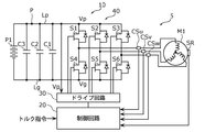
図1は、実施の形態1に係る車両駆動装置を備える電気車両を例示する図である。電気車両1は、駆動輪2と、動力伝達機構3と、永久磁石モータM1と、インバータ10と、電池P1とを備えている。これらの構成のうち、車両駆動装置5は、永久磁石モータM1、インバータ10および電池P1によって構成されている。以下、永久磁石モータM1をモータM1と呼ぶ場合がある。
FIG. 1 is a diagram illustrating an electric vehicle including the vehicle drive device according to the first embodiment. The
モータM1は、電気車両1の駆動輪2を駆動する三相交流式のモータであり、例えば、埋込磁石同期モータまたは表面磁石同期モータなどのモータが用いられる。
The motor M1 is a three-phase AC motor that drives the
動力伝達機構3は、例えば、ディファレンシャルギアおよびドライブシャフトによって構成され、モータM1と駆動輪2との間にて動力を伝達する。モータM1の回転力は、動力伝達機構3を経由して駆動輪2に伝達される。これと同様に、駆動輪2の回転力は、動力伝達機構3を経由してモータM1に伝達される。なお、電気車両1は、動力伝達機構3を備えていなくてもよく、モータM1と駆動輪2とが直結された構造であってもよい。
The
電池P1は、例えば、リチウムイオン電池などの直流電源である。電池P1は、モータM1を駆動させるための電力を供給し、および、この電力を蓄積する。 The battery P1 is a DC power source such as a lithium ion battery. The battery P1 supplies and stores electric power for driving the motor M1.
インバータ10は、電池P1から供給された直流電力を例えば三相の交流電力に変換して、その交流電力をモータM1に供給する電力変換装置の一例である。このように車両駆動装置5は、電池P1の電力を用いて三相交流式のモータM1を駆動するように構成されている。
The
図2は、実施の形態1に係る車両駆動装置の回路図である。なお、図2に示す電圧Vpは電源電圧であり、電圧Vgは接地電圧である。 FIG. 2 is a circuit diagram of the vehicle drive device according to the first embodiment. The voltage Vp shown in FIG. 2 is the power supply voltage, and the voltage Vg is the ground voltage.
図2に示すように、車両駆動装置5は、モータM1と、インバータ10と、電池P1とを備えている。
As shown in FIG. 2, the
[2.インバータ]
インバータ10は、三相インバータ回路40とドライブ回路30と制御回路20とを備えている。三相インバータ回路40は、電池P1から供給された直流電力をスイッチング動作により三相の交流電力に変換して、その交流電力をモータM1に供給し、モータM1を駆動する回路である。三相インバータ回路40の入力側はドライブ回路30に接続され、出力側はモータM1に接続されている。
[2. Inverter]
The
具体的には、三相インバータ回路40は、図2の上側に位置する上側アーム群に設けられたスイッチ素子S1、S2、S3(ハイサイドスイッチ素子)と、図2の下側に位置する下側アーム群に設けられたスイッチ素子S4、S5、S6(ローサイドスイッチ素子)とを備えている。例えば、スイッチ素子S1〜S6は、電界効果トランジスタ(FET)または絶縁ゲートバイポーラトランジスタ(IGBT)などによって構成される。また、スイッチ素子S1〜S6は、ワイドバンドギャップ半導体を用いて構成されてもよい。
Specifically, the three-
各スイッチ素子S1、S2、S3は、モータM1の3つの端子から引き出された3つの出力線と、電池P1の正極に接続された電源線Lpとの間のそれぞれの間に接続されている。各スイッチ素子S4、S5、S6は、上記3つの出力線と電池P1の負極に接続された接地線Lgとの間のそれぞれの間に接続されている。また、各スイッチ素子S1〜S6には、還流ダイオードが並列接続されている。還流ダイオードは、スイッチ素子S1〜S6に寄生する寄生ダイオードであってもよい。スイッチ素子S1、S4は、モータM1のU相に電気的に接続されており、スイッチ素子S1がU相のハイサイドスイッチ素子であり、スイッチ素子S4がU相のローサイドスイッチ素子である。スイッチ素子S2、S5は、モータM1のV相に電気的に接続されており、スイッチ素子S2がV相のハイサイドスイッチ素子であり、スイッチ素子S5がV相のローサイドスイッチ素子である。スイッチ素子S3、S6は、モータM1のW相に電気的に接続されており、スイッチ素子S3がW相のハイサイドスイッチ素子であり、スイッチ素子S6がW相のローサイドスイッチ素子である。 The switch elements S1, S2, and S3 are connected between the three output lines drawn from the three terminals of the motor M1 and the power supply line Lp connected to the positive electrode of the battery P1. The switch elements S4, S5, and S6 are connected between the above three output lines and the ground wire Lg connected to the negative electrode of the battery P1. Further, a freewheeling diode is connected in parallel to each of the switch elements S1 to S6. The freewheeling diode may be a parasitic diode parasitic on the switch elements S1 to S6. The switch elements S1 and S4 are electrically connected to the U phase of the motor M1, the switch element S1 is a U phase high side switch element, and the switch element S4 is a U phase low side switch element. The switch elements S2 and S5 are electrically connected to the V phase of the motor M1, the switch element S2 is a V phase high side switch element, and the switch element S5 is a V phase low side switch element. The switch elements S3 and S6 are electrically connected to the W phase of the motor M1, the switch element S3 is a W phase high side switch element, and the switch element S6 is a W phase low side switch element.
各スイッチ素子S1〜S6は、ドライブ回路30に接続され、ドライブ回路30から出力された信号によって駆動する。モータM1は、各スイッチ素子S1〜S6の駆動に基づいて、力行、回生または惰行などの状態で駆動される。
The switch elements S1 to S6 are connected to the
また、インバータ10には、三相インバータ回路40に印加される電圧を平滑化する複数のコンデンサが設けられている。ここで、複数のコンデンサは、セラミックコンデンサC1と、ハイブリッドコンデンサC2と、電解コンデンサC3とを含んでいる。
Further, the
セラミックコンデンサC1は、第一キャパシタの一例であり、一方の端子が電源線Lpに接続され、他方の端子が接地線Lgに接続されている。ハイブリッドコンデンサC2は、第二キャパシタの一例であり、一方の端子が電源線Lpに接続され、他方の端子が接地線Lgに接続されている。ハイブリッドコンデンサC2は、電解質に導電性高分子と電解液とを融合させたコンデンサである。ハイブリッドコンデンサC2は、例えば導電性高分子ハイブリッドアルミ電解コンデンサと称される場合もある。電解コンデンサC3は、第三キャパシタの一例であり、一方の端子が電源線Lpに接続され、他方の端子が接地線Lgに接続されている。 The ceramic capacitor C1 is an example of the first capacitor, one terminal is connected to the power supply line Lp, and the other terminal is connected to the ground wire Lg. The hybrid capacitor C2 is an example of a second capacitor, one terminal of which is connected to the power supply line Lp and the other terminal of which is connected to the ground wire Lg. The hybrid capacitor C2 is a capacitor in which a conductive polymer and an electrolytic solution are fused with an electrolyte. The hybrid capacitor C2 may be referred to as, for example, a conductive polymer hybrid aluminum electrolytic capacitor. The electrolytic capacitor C3 is an example of a third capacitor, one terminal of which is connected to the power supply line Lp and the other terminal of which is connected to the ground wire Lg.
図2に示すように、配線経路上において、セラミックコンデンサC1は、ハイブリッドコンデンサC2と、電解コンデンサC3とに比べて各スイッチ素子S1〜S6に近い位置に接続されている。また、電解コンデンサC3は、配線経路上において、ハイブリッドコンデンサC2に比べて各スイッチ素子S1〜S6から遠い位置に接続されている。つまり、各スイッチ素子S1〜S6から、セラミックコンデンサC1、ハイブリッドコンデンサC2、電解コンデンサC3という順でこれらが並んで配置されている。したがって、配線経路における寄生インダクタンスの大きさは、セラミックコンデンサC1、ハイブリッドコンデンサC2、電解コンデンサC3の順に大きくなる。 As shown in FIG. 2, the ceramic capacitor C1 is connected to the hybrid capacitor C2 at a position closer to the switch elements S1 to S6 than the electrolytic capacitor C3 on the wiring path. Further, the electrolytic capacitor C3 is connected to a position farther from each switch element S1 to S6 on the wiring path than the hybrid capacitor C2. That is, from each switch element S1 to S6, the ceramic capacitor C1, the hybrid capacitor C2, and the electrolytic capacitor C3 are arranged side by side in this order. Therefore, the magnitude of the parasitic inductance in the wiring path increases in the order of the ceramic capacitor C1, the hybrid capacitor C2, and the electrolytic capacitor C3.
ここで、本実施の形態の三種のコンデンサについて、その役割を図3を用いて説明する。図3は、実施の形態1に係る各キャパシタの単位体積当たりの容量と適応周波数の概略相関図である。図3において、横軸は単位体積当たりの容量を、縦軸は適応周波数(対数)を、それぞれ示す。 Here, the roles of the three types of capacitors of the present embodiment will be described with reference to FIG. FIG. 3 is a schematic correlation diagram of the capacitance per unit volume and the applicable frequency of each capacitor according to the first embodiment. In FIG. 3, the horizontal axis represents the capacity per unit volume, and the vertical axis represents the adaptive frequency (logarithm).
自動車の駆動用インバータのような電力変換装置における平滑コンデンサの役割は、(1)EMI対策、(2)スイッチ素子を構成する半導体の耐圧破壊保護のためのサージ抑制、(3)直流系統の安定化のためのリプル電流抑制、(4)脈動電流や異常時の電流吸収などがある。(1)のEMI対策について、インバータ10に大電流を流すとき、例えば5〜20kHzの周波数でスイッチ素子S1〜S6をスイッチング動作させる際に、大電流のスイッチングに起因する高次高調波ノイズが、電磁ノイズ(高周波ノイズ)として外部に放射されるが、その周波数は例えば最大数100MHzとなる。したがって、平滑コンデンサとして、数100MHzオーダーの高周波特性が必要となる。この場合、容量はあまり必要としない。(2)のサージ抑制は、例えば5〜20kHzの周波数でスイッチ素子S1〜S6をスイッチング動作させる際に、回路上の寄生インダクタンスと電流に基づいて発生する、例えば数MHzオーダーのサージを抑制するために、サージの周波数帯域でインピーダンスの低い平滑コンデンサが必要となる。この場合、(1)のEMI対策よりは容量が必要ではあるが、それほどの大容量は必要としない。
The roles of smoothing capacitors in power converters such as automobile drive inverters are (1) EMI countermeasures, (2) surge suppression to protect the withstand voltage of semiconductors that make up switch elements, and (3) stability of the DC system. There are ripple current suppression for conversion, (4) pulsating current and current absorption at the time of abnormality. Regarding the EMI countermeasure of (1), when a large current is passed through the
一方で、(4)の、特に異常時の電流吸収は、例えば回生ブレーキで電池を充電しているような状況で、電池のリレーが何らかのトラブルで開放されたような場合、回生電流の行き場が無くなり、全て平滑コンデンサに充電されることになる。そのため、平滑コンデンサの電圧が急上昇する。このとき、インバータの制御回路の指示で回生を停止させたとしても、モータ巻線に蓄えられた電流は残存するため、これを吸収するために十分な容量の平滑コンデンサが必要となる。しかし、この動作は例えば数十〜数百ミリ秒と遅いため、周波数帯域は例えば数百Hzまでとなり、高周波特性に優れたコンデンサなどは必要としない。 On the other hand, the current absorption in (4), especially at the time of abnormality, is the place where the regenerative current goes when the relay of the battery is opened due to some trouble in the situation where the battery is being charged by the regenerative brake, for example. It will disappear and all will be charged to the smoothing capacitor. Therefore, the voltage of the smoothing capacitor rises sharply. At this time, even if the regeneration is stopped by the instruction of the control circuit of the inverter, the current stored in the motor winding remains, so a smoothing capacitor having a sufficient capacity is required to absorb the current. However, since this operation is slow, for example, several tens to several hundred milliseconds, the frequency band is, for example, several hundred Hz, and a capacitor having excellent high frequency characteristics is not required.
また、(3)のリプル抑制は、(1)のEMI対策および(2)のサージ抑制と、(4)の脈動電流や異常時の電流吸収に対して、中間的な容量と周波数特性(例えば5〜20kHz)の平滑コンデンサが必要となる。 In addition, the ripple suppression in (3) has intermediate capacitance and frequency characteristics (for example) with respect to the EMI countermeasures in (1), the surge suppression in (2), and the pulsating current and current absorption in the event of an abnormality in (4). A smoothing capacitor of 5 to 20 kHz) is required.
これらのことから、図3を参照すると、(1)のEMI対策および(2)のサージ抑制にはセラミックコンデンサC1が適用できることがわかる。また、(3)のリプル抑制には、フィルムコンデンサ、またはハイブリッドコンデンサC2が適用できるが、単位体積当たりの容量が大きいハイブリッドコンデンサC2を適用することで小型化が図れる。(4)の脈動電流や異常時の電流吸収に対しては、電解コンデンサC3が適用できることがわかる。 From these facts, it can be seen that the ceramic capacitor C1 can be applied to the EMI countermeasure of (1) and the surge suppression of (2) with reference to FIG. Further, a film capacitor or a hybrid capacitor C2 can be applied to suppress the ripple in (3), but miniaturization can be achieved by applying a hybrid capacitor C2 having a large capacity per unit volume. It can be seen that the electrolytic capacitor C3 can be applied to the pulsating current of (4) and the current absorption at the time of abnormality.
次に、セラミックコンデンサC1、ハイブリッドコンデンサC2、電解コンデンサC3の周波数特性について、さらに詳細に説明する。図4は、実施の形態1に係る各キャパシタ(セラミックコンデンサC1、ハイブリッドコンデンサC2、電解コンデンサC3)のインピーダンスの周波数特性図である。図4において、横軸は周波数(対数)、縦軸はインピーダンスである。図4より、セラミックコンデンサC1は、EMIにつながる高周波ノイズやサージの周波数帯域(例えば数MHzオーダーから数100MHz)において、ハイブリッドコンデンサC2、電解コンデンサC3よりもインピーダンスが低い。ハイブリッドコンデンサC2は、リプルの周波数帯域(例えば5〜20kHz)において、セラミックコンデンサC1、電解コンデンサC3よりもインピーダンスが低い。電解コンデンサC3は、リプルよりも低い周波数帯域、すなわち、脈動電流や異常時においてモータM1から発生する電流の周波数帯域(例えば数百Hz)において、セラミックコンデンサC1、ハイブリッドコンデンサC2よりもインピーダンスが低い。したがって、上記した周波数帯域で最もインピーダンスの小さいコンデンサを使用することにより、各周波数帯域において自己発熱を抑制した平滑機能を実現することができる。 Next, the frequency characteristics of the ceramic capacitor C1, the hybrid capacitor C2, and the electrolytic capacitor C3 will be described in more detail. FIG. 4 is a frequency characteristic diagram of the impedance of each capacitor (ceramic capacitor C1, hybrid capacitor C2, electrolytic capacitor C3) according to the first embodiment. In FIG. 4, the horizontal axis is frequency (logarithm) and the vertical axis is impedance. From FIG. 4, the ceramic capacitor C1 has a lower impedance than the hybrid capacitor C2 and the electrolytic capacitor C3 in the frequency band of high frequency noise and surge connected to EMI (for example, from several MHz order to several hundred MHz). The hybrid capacitor C2 has a lower impedance than the ceramic capacitor C1 and the electrolytic capacitor C3 in the ripple frequency band (for example, 5 to 20 kHz). The electrolytic capacitor C3 has a lower impedance than the ceramic capacitor C1 and the hybrid capacitor C2 in a frequency band lower than the ripple, that is, a frequency band of a pulsating current or a current generated from the motor M1 at the time of abnormality (for example, several hundred Hz). Therefore, by using the capacitor having the lowest impedance in the frequency band described above, it is possible to realize a smoothing function in which self-heating is suppressed in each frequency band.
また、各コンデンサの使用周波数帯域におけるインピーダンス(図4の楕円で囲んだ領域)は、セラミックコンデンサC1、ハイブリッドコンデンサC2及び電解コンデンサC3の順で大きい。したがって、電解コンデンサC3は他のコンデンサに比べ、最も自己発熱が大きくなる。 Further, the impedance in the frequency band used of each capacitor (the region surrounded by the ellipse in FIG. 4) is larger in the order of the ceramic capacitor C1, the hybrid capacitor C2, and the electrolytic capacitor C3. Therefore, the electrolytic capacitor C3 has the largest self-heating as compared with other capacitors.
これらの特性に基づいて、各コンデンサは次のように適用できる。 Based on these characteristics, each capacitor can be applied as follows.
セラミックコンデンサC1(第一キャパシタ)は、ハイブリッドコンデンサC2及び電解コンデンサC3に比べ、サージの周波数帯域におけるインピーダンスが小さく、かつ、配線経路上、スイッチ素子に対して近い位置に配置されており、配線経路に起因する寄生インダクタンスも小さい。これにより、スイッチ素子S1〜S6に最も近いセラミックコンデンサC1は、高周波数帯域の平滑に適用でき、例えば数100MHzの高周波ノイズと数MHzオーダーのサージを抑制することができる。 The ceramic capacitor C1 (first capacitor) has a smaller impedance in the surge frequency band than the hybrid capacitor C2 and the electrolytic capacitor C3, and is arranged at a position closer to the switch element on the wiring path. The parasitic inductance caused by is also small. As a result, the ceramic capacitor C1 closest to the switch elements S1 to S6 can be applied to smoothing the high frequency band, and for example, high frequency noise of several hundred MHz and surge of several MHz order can be suppressed.
スイッチ素子S1〜S6に最も遠い電解コンデンサC3(第三キャパシタ)は、リプルの周波数帯域よりも低い、脈動電流や異常時の電流における周波数帯域(例えば数百Hzまで)において、セラミックコンデンサC1及びハイブリッドコンデンサC2に比べ、最もインピーダンスが小さいので、この周波数帯域における自己発熱を抑制しつつ、高周波ノイズ、サージ、あるいはリプルよりも大幅に低周波な脈動電流を平滑化したり、異常時の電流を吸収することができる。なお、電解コンデンサC3は、セラミックコンデンサC1及びハイブリッドコンデンサC2に比べ、配線経路上、スイッチ素子S1〜S6に対して遠い位置に配置されており、配線経路に起因する寄生インダクタンスは大きくなる。これにより、リプルの周波数帯域におけるリプル電流が抑制されるので、リプル電流に起因した第三キャパシタの自己発熱を抑制することもできる。さらに、電解コンデンサC3は、セラミックコンデンサC1及びハイブリッドコンデンサC2と比べて、それぞれの使用周波数帯域におけるインピーダンスが大きいため、自己発熱も相対的に大きくなる。そのため、配線経路上最も遠い位置に配置されている。これにより、電解コンデンサC3は、熱源であるスイッチ素子S1〜S6から離れて配置されるために、自己発熱に加えてスイッチ素子S1〜S6からの熱も受けてしまうという可能性を低減している。 The electrolytic capacitor C3 (third capacitor) farthest from the switch elements S1 to S6 is a hybrid with the ceramic capacitor C1 in the frequency band (for example, up to several hundred Hz) in the pulsating current or the abnormal current, which is lower than the frequency band of the ripple. Since it has the smallest impedance compared to the capacitor C2, it smoothes pulsating currents that are significantly lower than high-frequency noise, surges, or ripples, and absorbs abnormal currents while suppressing self-heating in this frequency band. be able to. The electrolytic capacitor C3 is arranged at a position farther from the switch elements S1 to S6 on the wiring path than the ceramic capacitor C1 and the hybrid capacitor C2, and the parasitic inductance caused by the wiring path is large. As a result, the ripple current in the ripple frequency band is suppressed, so that the self-heating of the third capacitor due to the ripple current can also be suppressed. Further, since the electrolytic capacitor C3 has a larger impedance in each used frequency band than the ceramic capacitor C1 and the hybrid capacitor C2, the self-heating is also relatively large. Therefore, it is arranged at the farthest position on the wiring path. As a result, since the electrolytic capacitor C3 is arranged away from the switch elements S1 to S6 which are heat sources, the possibility of receiving heat from the switch elements S1 to S6 in addition to self-heating is reduced. ..
また、配線経路上、セラミックコンデンサC1及び電解コンデンサC3の中間に配置されたハイブリッドコンデンサC2(第二キャパシタ)は、リプルの周波数帯域(例えば5〜20kHz)におけるインピーダンスが、セラミックコンデンサC1及び電解コンデンサC3より小さいので、リプルによる自己発熱を抑制することができる。なお、ハイブリッドコンデンサC2の、配線経路における寄生インダクタンスは、セラミックコンデンサC1及び電解コンデンサC3の中間の大きさとなるが、この寄生インダクタンスとハイブリッドコンデンサC2がリプル電流を透過させるフィルタの役割を果たすため、ハイブリッドコンデンサC2と電解コンデンサC3における自己発熱の最適化が可能となる。 Further, the hybrid capacitor C2 (second capacitor) arranged between the ceramic capacitor C1 and the electrolytic capacitor C3 on the wiring path has an impedance in the ripple frequency band (for example, 5 to 20 kHz) of the ceramic capacitor C1 and the electrolytic capacitor C3. Since it is smaller, self-heating due to ripple can be suppressed. The parasitic inductance of the hybrid capacitor C2 in the wiring path is an intermediate size between the ceramic capacitor C1 and the electrolytic capacitor C3. Since the parasitic inductance and the hybrid capacitor C2 act as a filter for transmitting the ripple current, the hybrid capacitor C2 is hybrid. It is possible to optimize the self-heating of the capacitor C2 and the electrolytic capacitor C3.
上記した各コンデンサの役割と、容量、サイズに応じて、各コンデンサの合計の体積が最小となる組み合わせの実例を以下に示す。なお、セラミックコンデンサC1は容量が小さいことから、そのサイズもハイブリッドコンデンサC2及び電解コンデンサC3に比べて極めて小さいため、合計体積を求める際に無視する。したがって、ここでは、ハイブリッドコンデンサC2と電解コンデンサC3の合計体積を最小にする実例を述べる。 An example of the combination in which the total volume of each capacitor is minimized according to the role of each capacitor and the capacity and size described above is shown below. Since the ceramic capacitor C1 has a small capacitance, its size is also extremely small as compared with the hybrid capacitor C2 and the electrolytic capacitor C3, so that it is ignored when calculating the total volume. Therefore, here, an example of minimizing the total volume of the hybrid capacitor C2 and the electrolytic capacitor C3 will be described.
まず、サイズについて、ハイブリッドコンデンサC2と電解コンデンサC3との体積比は、1:5であるとする。つまり、1個の電解コンデンサC3は、1個のハイブリッドコンデンサC2の5倍の体積を有する。次に、ハイブリッドコンデンサC2と電解コンデンサC3を合計した必要容量値は一定であるとする。 First, regarding the size, it is assumed that the volume ratio of the hybrid capacitor C2 and the electrolytic capacitor C3 is 1: 5. That is, one electrolytic capacitor C3 has five times the volume of one hybrid capacitor C2. Next, it is assumed that the total required capacitance value of the hybrid capacitor C2 and the electrolytic capacitor C3 is constant.
この条件で、ハイブリッドコンデンサC2と電解コンデンサC3との個数を可変して、体積が最小となる組み合わせ個数を求めた。その結果、ハイブリッドコンデンサC2と電解コンデンサC3との個数比は、1:3であるときに体積が最小となった。この比率で構成した具体例は、後述する図5で説明する。また、従来のように二種類のコンデンサ(電解コンデンサとセラミックコンデンサ)で構成した場合と対比すると、セラミックコンデンサを無視して電解コンデンサC3だけで必要容量値を得るための体積を求めた結果、上記したハイブリッドコンデンサC2と電解コンデンサC3との個数比を1:3としたときの体積に比べると、約2倍であった。したがって、平滑コンデンサを従来の半分の体積にすることができる。 Under this condition, the number of the hybrid capacitor C2 and the electrolytic capacitor C3 was varied, and the number of combinations having the minimum volume was obtained. As a result, the volume of the hybrid capacitor C2 and the electrolytic capacitor C3 became the minimum when the number ratio was 1: 3. A specific example configured with this ratio will be described later with reference to FIG. In addition, as a result of finding the volume for obtaining the required capacitance value only with the electrolytic capacitor C3, ignoring the ceramic capacitor, as a result of comparing with the case of being composed of two types of capacitors (electrolytic capacitor and ceramic capacitor) as in the conventional case, the above It was about twice the volume when the number ratio of the hybrid capacitor C2 and the electrolytic capacitor C3 was 1: 3. Therefore, the smoothing capacitor can be reduced to half the volume of the conventional one.
このように、特にハイブリッドコンデンサC2と電解コンデンサC3との組み合わせを選定することで、平滑コンデンサ全体の体積を最小化でき、電力変換装置を小型化することが可能となる。なお、各スイッチ素子S1〜S6及び各コンデンサのレイアウトの具体例については後述する。 In this way, by particularly selecting the combination of the hybrid capacitor C2 and the electrolytic capacitor C3, the volume of the entire smoothing capacitor can be minimized, and the power conversion device can be miniaturized. Specific examples of the layout of each switch element S1 to S6 and each capacitor will be described later.
また、上記結果は一例であり、各コンデンサのサイズ、容量は多種類があるため、使用する各コンデンサに応じて、適宜、最適な組み合わせ個数を求めればよい。 Further, the above result is an example, and since there are various sizes and capacities of each capacitor, the optimum number of combinations may be appropriately obtained according to each capacitor to be used.
ここで、図2に戻り、ドライブ回路30は、三相PWM制御を実行するため、三相インバータ回路40のスイッチ素子S1〜S6を駆動する回路である。ドライブ回路30の入力側は制御回路20に接続され、出力側は三相インバータ回路40に接続されている。なお、ドライブ回路30は、三相短絡制御を実行するために、三相インバータ回路40のスイッチ素子S1〜S6を駆動してもよい。
Here, returning to FIG. 2, the
制御回路20は、各種の演算等を行うマイクロプロセッサと、マイクロプロセッサを動作させるためのプログラムまたは情報などを記憶するメモリとによって構成される。
The
制御回路20は、モータM1に流れる電流を検知する電流センサCSu、CSv、CSw及びモータM1の磁極位置を検出して回転位置を検知する回転位置センサRSなどの各種センサによって検知された情報を取得する。なお、電流センサCSu、CSv、CSwは、モータM1のU相、V相、W相における電流値を検知するセンサである。また、制御回路20は、電源線Lpにおける電圧Vpに関する情報を取得する。また、制御回路20は、当該制御回路20の外部、例えば電気車両1のECU(Engine Control Unit)から出力されたトルク指令などの制御指令情報を取得する。
The
制御回路20は、取得した上記情報を演算により変換し、モータM1を制御するための制御信号を求める。例えば、制御回路20は、車両駆動装置5の運行時におけるモータM1のトルクが、トルク指令情報に示された目標トルク(例えば電気車両1のアクセルペダルの操作量に応じたトルク)となるように制御信号を求める。制御回路20は、求めた制御信号に基づいて、モータM1を駆動するために必要な駆動信号を演算し、この駆動信号をドライブ回路30に出力する。制御回路20は、車両駆動装置5が通常運行している際は、三相PWM制御を行うための駆動信号を出力する。
The
このように、制御回路20は、三相PWM制御を実行するための駆動信号をドライブ回路30に出力する。ドライブ回路30では、制御回路20から出力された駆動信号を三相インバータ回路40に出力する。三相インバータ回路40は、ドライブ回路30から出力された信号に基づいて、モータM1を駆動する。
In this way, the
[3.各スイッチ素子及び各コンデンサのレイアウト]
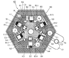
次に、各スイッチ素子S1〜S6及び各コンデンサのレイアウトについて説明する。図5は、実施の形態1に係る各スイッチ素子及び各コンデンサのレイアウトを示す平面図である。
[3. Layout of each switch element and each capacitor]
Next, the layout of each switch element S1 to S6 and each capacitor will be described. FIG. 5 is a plan view showing the layout of each switch element and each capacitor according to the first embodiment.
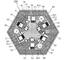
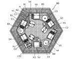
図5に示すように、三相インバータ回路40は、例えば正六角形状の基板80を有しており、この基板80に対して、各スイッチ素子S1〜S6及び各コンデンサ(セラミックコンデンサC1及びハイブリッドコンデンサC2)が設けられている。
As shown in FIG. 5, the three-
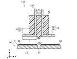
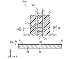
具体的には、基板80の一方の主面には、第一導電パターン81と、第二導電パターン82と、U相導電パターン83と、V相導電パターン84と、W相導電パターン85とが設けられている。第一導電パターン81は、正極側の導電パターンであり、外形が正六角形状となっている。第一導電パターン81には、電源線Lpに接続される第一バスバー71が、基板80の他方の主面側から電気的に接続されている。第一導電パターン81の内方には、開口部811が設けられている。開口部811は、基板80の中央に位置する中央開口部812と、中央開口部812から張り出された3つの張出部813、814、815とを有している。
Specifically, on one main surface of the
中央開口部812内には、第二導電パターン82が配置されている。第二導電パターン82は、負極側の導電パターンであり、第一導電パターン81とは接触しない形状に形成されている。第二導電パターン82には、接地線Lgに接続される第二バスバー72が、基板80の他方の主面側から電気的に接続されている。第一バスバー71及び第二バスバー72には、基板80の外方となる位置で電解コンデンサC3が電気的に接続されている。
A second
ここで、第一バスバー71及び第二バスバー72について説明する。本実施の形態では、ハイブリッドコンデンサC2(第二キャパシタ)と電解コンデンサC3(第三キャパシタ)との間の配線経路は、上記したリプルの周波数帯域のリプル電流の透過を抑制するようにフィルタを構成している。具体的には、この配線経路として、第一バスバー71及び第二バスバー72が用いられる。そして、ハイブリッドコンデンサC2と電解コンデンサC3の各々の容量値と、リプルの周波数帯域とから、第一バスバー71及び第二バスバー72の寄生インダクタンスがフィルタとして機能する値になるように、第一バスバー71及び第二バスバー72の形状、サイズ、材質の少なくともいずれかを決定している。形状としては、図5の構成では平板状としているが、それに限定されず、それぞれのバスバーの長手方向断面形状がコの字状、あるいは、Uの字状にすることにより、寄生インダクタンスの値を大きくする方向に調整してもよい。また、バスバーの形状として長さを調整することも可能である。一般的にはバスバーは最短距離で対象物同士を接続することが求められるが、そのバスバーの長さを最短距離よりも長大化することで、寄生インダクタンスの値を大きくすることも可能である。また、サイズについては、それぞれのバスバーの長さ、幅、厚みにより、所望の寄生インダクタンスが得られるようにしている。また、材質については、抵抗値の違う導電材料から適切な材料を選択すればよい。バスバーとなりうる導電材料としては、例えばアルミニウム、銅、鉄、真鍮、これらの合金などが挙げられる。このように、それぞれのバスバーの形状、サイズ、材質の少なくともいずれかを調整することにより、容易に寄生インダクタンスを調整できる。
Here, the
このようにして、第一バスバー71及び第二バスバー72の形状、サイズを決定することで、ハイブリッドコンデンサC2から電解コンデンサC3に至る配線経路の寄生インダクタンスを利用して、電解コンデンサC3へのリプル電流を抑制するフィルタを構成している。その結果、電解コンデンサC3は、リプル電流に起因する自己発熱が抑制されるため、耐熱目的で大型化していた電解コンデンサC3を小型化することができる。
By determining the shapes and sizes of the
なお、本実施の形態では、ハイブリッドコンデンサC2から電解コンデンサC3に至る配線経路をバスバーで構成したが、それに限定されるものではなく、第一導電パターン81及び第二導電パターン82のパターン形状や長さにより、寄生インダクタンスを調整してもよい。ただし、第一導電パターン81及び第二導電パターン82は平面上に形成されるため、所望の寄生インダクタンスを得るには、パターンが長くなってしまう。電力変換装置の小型化のためには、立体的な配線も可能なバスバーを配線経路に適用する方が望ましい。
In the present embodiment, the wiring path from the hybrid capacitor C2 to the electrolytic capacitor C3 is configured by a bus bar, but the wiring path is not limited to that, and the pattern shape and length of the first
3つの張出部813、814、815のそれぞれは、基板80の主面内に配置された仮想的な正六角形Hに沿うように延設されている。仮想的な正六角形Hは、基板80と同心であることがよい。仮想的な正六角形Hの各辺を、第一辺h1、第二辺h2、第三辺h3、第四辺h4、第五辺h5、第六辺h6とする。図5においては、第一辺h1を基準とすると、第二辺h2、第三辺h3、第四辺h4、第五辺h5及び第六辺h6がこの順で反時計回りに配列されている。
Each of the three overhanging
張出部813内にはU相導電パターン83が配置されている。U相導電パターン83は、モータM1のU相に対して電気的に接続されている。U相導電パターン83は、第一導電パターン81と第二導電パターン82とに接触しないように、第一辺h1及び第二辺h2に沿った形状に形成されている。U相導電パターン83には、U相のハイサイドスイッチ素子であるスイッチ素子S1と、U相のローサイドスイッチ素子であるスイッチ素子S4とが電気的に接続されている。具体的には、スイッチ素子S1は、ドレイン端子とソース端子との並び方向が第一辺h1に交差するように配置されている。スイッチ素子S1は、ドレイン端子が第一導電パターン81に電気的に接続され、ソース端子がU相導電パターン83に電気的に接続されている。スイッチ素子S1のゲート端子は、U相導電パターン83から離間しており、U相導電パターン83とは非導通となっている。例えば、U相導電パターン83に切り欠きを設けて、ゲート端子をゲート用導電パターンと接続することで、当該U相導電パターン83とゲート端子とを非導通にしてもよいし(例えば図8参照)、ゲート端子をU相導電パターン83から浮かせて非導通にしてもよい。これは他のスイッチ素子S2〜S6において同様である。本実施の形態では、導電パターンに切り欠きを設けて、ゲート端子をゲート用導電パターンと接続することで、導電パターンとゲート端子とを非導通にしているが、図5では図面の煩雑さを避けるために、導電パターンの切り欠き部分、および、ゲート用導電パターンを省略している。なお、以後、説明する図6、図11、および、図12においても、図5と同様に導電パターンの切り欠き部分を省略している。また、図6と図8〜図12においても、図5と同様にゲート用導電パターンを省略している。
A U-phase
スイッチ素子S4は、ドレイン端子とソース端子との並び方向が第二辺h2に交差するように配置されている。スイッチ素子S4は、ドレイン端子がU相導電パターン83に電気的に接続され、ソース端子が第二導電パターン82に電気的に接続されている。なお、スイッチ素子S4のゲート端子は、第二導電パターン82から離間しており、第二導電パターン82とは非導通となっている。
The switch element S4 is arranged so that the arrangement direction of the drain terminal and the source terminal intersects the second side h2. In the switch element S4, the drain terminal is electrically connected to the U-phase
張出部814内にはV相導電パターン84が配置されている。V相導電パターン84は、モータM1のV相に対して電気的に接続されている。V相導電パターン84は、第一導電パターン81と第二導電パターン82とに接触しないように、第三辺h3及び第四辺h4に沿った形状に形成されている。V相導電パターン84には、V相のハイサイドスイッチ素子であるスイッチ素子S2と、V相のローサイドスイッチ素子であるスイッチ素子S5とが電気的に接続されている。具体的には、スイッチ素子S2は、ドレイン端子とソース端子との並び方向が第三辺h3に交差するように配置されている。スイッチ素子S2は、ドレイン端子が第一導電パターン81に電気的に接続され、ソース端子がV相導電パターン84に電気的に接続されている。スイッチ素子S2のゲート端子は、V相導電パターン84から離間しており、V相導電パターン84とは非導通となっている。スイッチ素子S5は、ドレイン端子とソース端子との並び方向が第四辺h4に交差するように配置されている。スイッチ素子S5は、ドレイン端子がV相導電パターン83に電気的に接続され、ソース端子が第二導電パターン82に電気的に接続されている。なお、スイッチ素子S5のゲート端子は、第二導電パターン82から離間しており、第二導電パターン82とは非導通となっている。
A V-phase
張出部815内にはW相導電パターン85が配置されている。W相導電パターン85は、モータM1のW相に対して電気的に接続されている。W相導電パターン85は、第一導電パターン81と第二導電パターン82とに接触しないように、第五辺h5及び第六辺h6に沿った形状に形成されている。W相導電パターン85には、W相のハイサイドスイッチ素子であるスイッチ素子S3と、W相のローサイドスイッチ素子であるスイッチ素子S6とが電気的に接続されている。具体的には、スイッチ素子S3は、ドレイン端子とソース端子との並び方向が第五辺h5に交差するように配置されている。スイッチ素子S3は、ドレイン端子が第一導電パターン81に電気的に接続され、ソース端子がW相導電パターン85に電気的に接続されている。スイッチ素子S3のゲート端子は、W相導電パターン85から離間しており、W相導電パターン84とは非導通となっている。スイッチ素子S6は、ドレイン端子とソース端子との並び方向が第六辺h6に交差するように配置されている。スイッチ素子S6は、ドレイン端子がW相導電パターン85に電気的に接続され、ソース端子が第二導電パターン82に電気的に接続されている。なお、スイッチ素子S6のゲート端子は、第二導電パターン82から離間しており、第二導電パターン82とは非導通となっている。
A W-phase
また、U相のスイッチ素子S1、S4と、V相のスイッチ素子S2、S5と、W相のスイッチ素子S3、S6とは、基板80の周方向に概ね均等となるように配置されている。
Further, the U-phase switch elements S1 and S4, the V-phase switch elements S2 and S5, and the W-phase switch elements S3 and S6 are arranged so as to be substantially uniform in the circumferential direction of the
また、基板80には、三対のセラミックコンデンサC1が設けられている。各対のセラミックコンデンサC1は、ハイサイドスイッチ素子である各スイッチ素子S1、S2、S3を周方向で挟むように配置されている。各対のセラミックコンデンサC1は、第一導電パターン81と第二導電パターン82に対して電気的に接続されている。
Further, the
基板80には3つのハイブリッドコンデンサC2が設けられている。各ハイブリッドコンデンサC2は、ハイサイドスイッチ素子である各スイッチ素子S1、S2、S3に対向する位置に配置されている。各ハイブリッドコンデンサC2は、第一導電パターン81と第二導電パターン82に対して電気的に接続されている。
The
ここで、一対のセラミックコンデンサC1のうち、少なくとも一つのセラミックコンデンサC1は、対応するハイブリッドコンデンサC2よりも、配線経路上において一組のスイッチ素子(ローサイドスイッチ素子及びハイサイドスイッチ素子)に近い位置に配置されている。 Here, at least one ceramic capacitor C1 of the pair of ceramic capacitors C1 is located closer to a set of switch elements (low-side switch element and high-side switch element) on the wiring path than the corresponding hybrid capacitor C2. Have been placed.
ここで、U相導電パターン83の周辺を例示して説明する。以下で説明する関係性は、V相、W相において同様である。
Here, the periphery of the U-phase
例えば、スイッチ素子S4を挟む一対のセラミックコンデンサC1のうち、スイッチ素子S1側のセラミックコンデンサC1は、スイッチ素子S1に対向するハイブリッドコンデンサC2よりも配線経路上において一組のスイッチ素子S1、S4に近い位置に配置されている。具体的には、スイッチ素子S1側のセラミックコンデンサC1の配線経路上の距離は、スイッチ素子S1との最短距離L1及びスイッチ素子S4との最短距離L2の合計値で表される。一方、ハイブリッドコンデンサC2の配線経路上の距離は、スイッチ素子S1との最短距離L11とスイッチ素子S4の最短距離L12との合計値で表される。この合計値が小さい方が、一組のスイッチ素子S1、S4に対して近い位置に配置されている。 For example, of the pair of ceramic capacitors C1 sandwiching the switch element S4, the ceramic capacitor C1 on the switch element S1 side is closer to the set of switch elements S1 and S4 on the wiring path than the hybrid capacitor C2 facing the switch element S1. It is placed in a position. Specifically, the distance on the wiring path of the ceramic capacitor C1 on the switch element S1 side is represented by the total value of the shortest distance L1 with the switch element S1 and the shortest distance L2 with the switch element S4. On the other hand, the distance on the wiring path of the hybrid capacitor C2 is represented by the total value of the shortest distance L11 with the switch element S1 and the shortest distance L12 with the switch element S4. The smaller of these total values is arranged at a position closer to the set of switch elements S1 and S4.
これに対し、電解コンデンサC3は、第一バスバー71及び第二バスバー72を介して第一導電パターン81及び第二導電パターン82に電気的に接続されている。このため、電解コンデンサC3は、配線経路上においてセラミックコンデンサC1及びハイブリッドコンデンサC2よりも、一組のスイッチ素子に対して最も遠い位置に配置されている。これにより、電解コンデンサC3がスイッチ素子S1〜S6からの熱の影響を受けにくくなる。
On the other hand, the electrolytic capacitor C3 is electrically connected to the first
また、図5の構成では、上記したハイブリッドコンデンサC2と電解コンデンサC3の個数を1:3とした例である。その前提条件は、上記した通り、ハイブリッドコンデンサC2と電解コンデンサC3との体積比が1:5とした。図5では電解コンデンサC3の直径がハイブリッドコンデンサC2の直径に近いが、電解コンデンサC3の高さがハイブリッドコンデンサC2の高さより大きいものを用いたため、体積比は1:5である。このように構成しているため、必要となるハイブリッドコンデンサC2と電解コンデンサC3との合計体積を最小化できるので、電力変換装置の小型化が可能となる。 Further, in the configuration of FIG. 5, the number of the hybrid capacitor C2 and the electrolytic capacitor C3 described above is 1: 3. As described above, the precondition is that the volume ratio of the hybrid capacitor C2 and the electrolytic capacitor C3 is 1: 5. In FIG. 5, the diameter of the electrolytic capacitor C3 is close to the diameter of the hybrid capacitor C2, but the volume ratio is 1: 5 because the height of the electrolytic capacitor C3 is larger than the height of the hybrid capacitor C2. Since it is configured in this way, the total volume of the required hybrid capacitor C2 and electrolytic capacitor C3 can be minimized, so that the power conversion device can be miniaturized.
なお、スイッチ素子S4を挟む一対のセラミックコンデンサC1のうち、スイッチ素子S1側ではない、つまり、スイッチ素子S4とスイッチ素子S2とで挟まれるセラミックコンデンサC1は、スイッチ素子S1との最短距離と、スイッチ素子S4との最短距離の合計値が、ハイブリッドコンデンサC2における最短距離L11と最短距離L12との合計値よりも大きくなる。したがって、セラミックコンデンサC1のすべてが、ハイブリッドコンデンサC2に比べて、一組のスイッチ素子S1、S4に対して近い位置に配置される必要はなく、一対のセラミックコンデンサC1のうち、少なくとも一つのセラミックコンデンサC1が一組のスイッチ素子S1、S4に対してハイブリッドコンデンサC2よりも近い位置に配置されていればよい。 Of the pair of ceramic capacitors C1 sandwiching the switch element S4, the ceramic capacitor C1 that is not on the switch element S1 side, that is, sandwiched between the switch element S4 and the switch element S2, has the shortest distance from the switch element S1 and the switch. The total value of the shortest distance to the element S4 is larger than the total value of the shortest distance L11 and the shortest distance L12 in the hybrid capacitor C2. Therefore, it is not necessary that all of the ceramic capacitors C1 are arranged closer to the pair of switch elements S1 and S4 than the hybrid capacitors C2, and at least one of the pair of ceramic capacitors C1 is a ceramic capacitor. It suffices that C1 is arranged at a position closer to the pair of switch elements S1 and S4 than the hybrid capacitor C2.
[4.効果など]
以上のように、本実施の形態に係る電力変換装置(インバータ10)は、基板80と、基板80上に設けられた複数のスイッチ素子S1〜S6と、スイッチ素子S1〜S6の直流電圧側の正極と負極の間にそれぞれ並列に電気的に接続される第一キャパシタ(セラミックコンデンサC1)、第二キャパシタ(ハイブリッドコンデンサC2)及び第三キャパシタ(電解コンデンサC3)とを備え、第一キャパシタは、第二キャパシタ及び第三キャパシタに比べて、配線経路上、スイッチ素子S1〜S6に近い位置に接続され、第三キャパシタは、第二キャパシタに比べて配線経路上、スイッチ素子S1〜S6から遠い位置に接続され、第一キャパシタは、第二キャパシタ及び第三キャパシタに比べて電磁妨害につながる高周波ノイズからサージまでの周波数帯域におけるインピーダンスが小さく、第二キャパシタは、第一キャパシタ及び第三キャパシタに比べてリプルの周波数帯域におけるインピーダンスが小さく、第三キャパシタは、第一キャパシタ及び第二キャパシタに比べてリプルの周波数帯域よりも低い周波数帯域におけるインピーダンスが小さい。
[4. Effect etc.]
As described above, the power conversion device (inverter 10) according to the present embodiment includes the
これによれば、第一キャパシタは、他のキャパシタに比べ、電磁妨害(EMI)につながる高周波ノイズからサージまでの周波数帯域におけるインピーダンスが小さく、かつ、配線経路上、スイッチ素子に対して近い位置に配置されており、配線経路に起因する寄生インダクタンスも小さい。これにより、スイッチ素子に最も近い第一キャパシタは、例えば数100MHzの高周波ノイズから数MHzオーダーのサージまでの高周波数帯域において、高周波ノイズとサージを抑制することができる。また、スイッチ素子に最も遠い第三キャパシタは、リプルの周波数帯域よりも低い、脈動電流や異常時の電流吸収における周波数帯域(例えば数百Hzまで)において、他のキャパシタに比べ、最もインピーダンスが小さいので、この周波数帯域における自己発熱を抑制しつつ、サージやリプルよりも大幅に低周波な脈動電流を吸収して平滑化したり、異常時の電流を吸収することができる。なお、第三キャパシタは、他のキャパシタに比べ、配線経路上、スイッチ素子に対して遠い位置に配置されており、配線経路に起因する寄生インダクタンスは大きくなる。これにより、リプルの周波数帯域におけるリプル電流が抑制されるので、リプル電流に起因した第三キャパシタの自己発熱を抑制することもできる。また、配線経路上、他のキャパシタの中間に配置された第二キャパシタは、リプルの周波数帯域(例えば5〜20kHz)におけるインピーダンスが他のキャパシタより小さいので、リプルによる自己発熱を抑制することができる。なお、第二キャパシタの、配線経路における寄生インダクタンスは、第一キャパシタ及び第三キャパシタの中間の大きさとなるが、この寄生インダクタンスと第二キャパシタがリプル電流を透過させるフィルタの役割を果たすため、第二キャパシタと第三キャパシタにおける自己発熱の最適化が可能となる。 According to this, the first capacitor has a smaller impedance in the frequency band from high frequency noise leading to electromagnetic interference (EMI) to surge than other capacitors, and is located closer to the switch element on the wiring path. It is arranged and the parasitic inductance caused by the wiring path is small. As a result, the first capacitor closest to the switch element can suppress high frequency noise and surge in a high frequency band ranging from high frequency noise of several hundred MHz to surge of several MHz order, for example. In addition, the third capacitor farthest from the switch element has the smallest impedance compared to other capacitors in the frequency band (for example, up to several hundred Hz) for pulsating current and current absorption at the time of abnormality, which is lower than the frequency band of ripple. Therefore, while suppressing self-heating in this frequency band, it is possible to absorb and smooth a pulsating current having a frequency significantly lower than that of a surge or ripple, or to absorb an abnormal current. The third capacitor is arranged at a position farther from the switch element on the wiring path than the other capacitors, and the parasitic inductance caused by the wiring path becomes large. As a result, the ripple current in the ripple frequency band is suppressed, so that the self-heating of the third capacitor due to the ripple current can also be suppressed. Further, since the impedance of the second capacitor arranged in the middle of the other capacitors on the wiring path is smaller than that of the other capacitors in the ripple frequency band (for example, 5 to 20 kHz), self-heating due to the ripple can be suppressed. .. The parasitic inductance of the second capacitor in the wiring path is an intermediate size between the first capacitor and the third capacitor, but since this parasitic inductance and the second capacitor act as a filter for transmitting the ripple current, the first capacitor It is possible to optimize self-heating in the second capacitor and the third capacitor.
このように、各役割に適した第一キャパシタ、第二キャパシタ及び第三キャパシタを設けることで、各役割を二種類のコンデンサで担う従来の場合よりも、各キャパシタを適切なサイズ、個数に設定することができる。したがって、第一キャパシタが高周波ノイズとサージを抑制するため、別途、大型のEMI対策用のフィルタ回路を設ける必要が無く、その分、小型化を図ることができる。さらに、第一キャパシタ、第二キャパシタ及び第三キャパシタの合計の体積が最小となる、各キャパシタのサイズ、個数の組み合わせを決定することで、インバータ10自体の小型化を図ることができる。
In this way, by providing the first capacitor, the second capacitor, and the third capacitor suitable for each role, each capacitor is set to an appropriate size and number as compared with the conventional case where each role is played by two types of capacitors. can do. Therefore, since the first capacitor suppresses high-frequency noise and surge, it is not necessary to separately provide a large filter circuit for EMI countermeasures, and the size can be reduced accordingly. Further, the size of the
ここで、第三キャパシタは、他のキャパシタと比べて、それぞれの使用周波数帯域におけるインピーダンスが大きいため、自己発熱も相対的に大きくなる。そのため、配線経路上最も遠い位置に配置されている。これにより、第三キャパシタは、熱源であるスイッチ素子S1〜S6から離れて配置されるために、自己発熱に加えてスイッチ素子からの熱も受けてしまうという可能性を低減している。また、第三キャパシタは、他のキャパシタと比べて容量が大きいためにサイズも大きいが、スイッチ素子S1〜S6から離れた位置であれば、空間的な自由度も高くなり、適切な位置に第三キャパシタを配置しやすくなる。 Here, since the third capacitor has a larger impedance in each used frequency band than the other capacitors, the self-heating is also relatively large. Therefore, it is arranged at the farthest position on the wiring path. As a result, since the third capacitor is arranged away from the switch elements S1 to S6 which are heat sources, the possibility of receiving heat from the switch element in addition to self-heating is reduced. Further, the third capacitor has a large capacity as compared with other capacitors, and therefore has a large size. However, if the third capacitor is located away from the switch elements S1 to S6, the degree of freedom in space is increased, and the third capacitor is placed at an appropriate position. It becomes easy to arrange three capacitors.
また、第二キャパシタと第三キャパシタとの間の配線経路は、リプルの周波数帯域のリプル電流の透過を抑制するように構成される。 Further, the wiring path between the second capacitor and the third capacitor is configured to suppress the transmission of the ripple current in the ripple frequency band.
この構成によれば、第二キャパシタから第三キャパシタに至る配線経路の寄生インダクタンスを利用して、第三キャパシタへのリプル電流を抑制するフィルタを構成することができる。その結果、第三キャパシタは、リプル電流に起因する自己発熱が抑制されるため、耐熱目的で大型化していた第三キャパシタを小型化することができる。 According to this configuration, it is possible to configure a filter that suppresses the ripple current to the third capacitor by utilizing the parasitic inductance of the wiring path from the second capacitor to the third capacitor. As a result, the third capacitor suppresses self-heating due to the ripple current, so that the third capacitor, which has been enlarged for the purpose of heat resistance, can be downsized.
また、第二キャパシタと第三キャパシタとの間の配線経路は、バスバーで構成される。 Further, the wiring path between the second capacitor and the third capacitor is composed of a bus bar.
この構成によれば、バスバーの形状、サイズにより、配線経路の寄生インダクタンスを調整でき、第二キャパシタ、第三キャパシタ、およびバスバーの寄生インダクタンスとで構成されるフィルタの周波数特性を、リプルの周波数帯域に合わせることが容易となる。 According to this configuration, the parasitic inductance of the wiring path can be adjusted according to the shape and size of the bus bar, and the frequency characteristics of the filter composed of the second capacitor, the third capacitor, and the parasitic inductance of the bus bar can be adjusted in the ripple frequency band. It becomes easy to match with.
また、第一キャパシタはセラミックコンデンサC1であり、第二キャパシタはハイブリッドコンデンサC2であり、第三キャパシタは電解コンデンサC3である。 The first capacitor is a ceramic capacitor C1, the second capacitor is a hybrid capacitor C2, and the third capacitor is an electrolytic capacitor C3.
これによれば、セラミックコンデンサが第一キャパシタであるので、上記した周波数帯域の中で、高周波帯域となる高周波ノイズおよびサージを効果的に抑制することができる。また、ハイブリッドコンデンサが第二キャパシタであるので、モータのスイッチング制御によって発生するリプルを効果的に抑制することができる。さらに、ハイブリッドコンデンサはフィルムコンデンサに比べて、単位体積当たりの容量が大きいので、リプルを抑制するために必要な容量を得るための体積がフィルムコンデンサより小さくなり、小型化を図ることができる。また、相対的に自己発熱の多い電解コンデンサを第三キャパシタとして用いた場合であっても、配線経路上、熱源であるスイッチ素子から最も遠い位置に配置されているので、電解コンデンサに対する、スイッチ素子からの熱の影響を受けにくくできる。さらに、配線経路における寄生インダクタンスが大きいことから、リプル電流に起因する自己発熱が抑制され、かつ、上記した周波数帯域の中で、周波数の低い脈動電流の抑制や異常時の電流吸収を効果的に実現することができる。 According to this, since the ceramic capacitor is the first capacitor, it is possible to effectively suppress high frequency noise and surge in the high frequency band in the above frequency band. Further, since the hybrid capacitor is the second capacitor, the ripple generated by the switching control of the motor can be effectively suppressed. Further, since the hybrid capacitor has a larger capacity per unit volume than the film capacitor, the volume for obtaining the capacity required for suppressing ripple is smaller than that of the film capacitor, and the size can be reduced. Further, even when an electrolytic capacitor having a relatively large amount of self-heating is used as the third capacitor, since it is located at the position farthest from the switch element which is a heat source on the wiring path, the switch element with respect to the electrolytic capacitor It can be less affected by the heat from. Furthermore, since the parasitic inductance in the wiring path is large, self-heating due to the ripple current is suppressed, and in the above-mentioned frequency band, suppression of low-frequency pulsating current and current absorption at the time of abnormality are effective. It can be realized.
また、複数のスイッチ素子S1〜S6は、三相インバータ回路40をなし、複数のスイッチ素子S1〜S6は、U相のハイサイドスイッチ素子、U相のローサイドスイッチ素子、V相のハイサイドスイッチ素子、V相のローサイドスイッチ素子、W相のハイサイドスイッチ素子及びW相のローサイドスイッチ素子を含み、U相のハイサイドスイッチ素子(スイッチ素子S1)は、基板80内に収まる仮想的な正六角形Hの第一辺h1に対して配置され、U相のローサイドスイッチ素子(スイッチ素子S4)は、正六角形Hの第一辺h1に隣り合う第二辺h2に対して配置され、V相のハイサイドスイッチ素子(スイッチ素子S2)は、正六角形Hの第二辺h2に隣り合う第三辺h3に対して配置され、V相のローサイドスイッチ素子(スイッチ素子S5)は、正六角形Hの第三辺h3に隣り合う第四辺h4に対して配置され、W相のハイサイドスイッチ素子(スイッチ素子S3)は、正六角形Hの第四辺h4に隣り合う第五辺h5に対して配置され、W相のローサイドスイッチ素子(スイッチ素子S6)は、正六角形Hの第五辺h5に隣り合う第六辺h6に対して配置されている。
Further, the plurality of switch elements S1 to S6 form a three-
これによれば、基板内に収まる仮想的な正六角形Hの各辺h1〜h6に対して各相のハイサイドスイッチ素子(スイッチ素子S1〜S3)とローサイドスイッチ素子(スイッチ素子S4〜S6)とが配置されているので、各スイッチ素子S1〜S6を均等に配置することができる。したがって、インバータ10をより小型にすることが可能である。
According to this, the high-side switch elements (switch elements S1 to S3) and the low-side switch elements (switch elements S4 to S6) of each phase are used for each side h1 to h6 of the virtual regular hexagon H that fits in the substrate. Are arranged, so that the switch elements S1 to S6 can be evenly arranged. Therefore, the
また、U相、V相、W相のいずれにおいても、セラミックコンデンサC1が一対ずつ設けられているので、各相に対するセラミックコンデンサC1によるサージの抑制効果をより抑制することが可能である。この場合、一対のセラミックコンデンサC1のそれぞれが、対応するハイブリッドコンデンサC2よりも、配線経路上において一組のスイッチ素子(ローサイドスイッチ素子及びハイサイドスイッチ素子)に近い位置に配置されていることが望ましい。 Further, since a pair of ceramic capacitors C1 are provided in each of the U phase, the V phase, and the W phase, it is possible to further suppress the surge suppressing effect of the ceramic capacitor C1 on each phase. In this case, it is desirable that each of the pair of ceramic capacitors C1 is arranged at a position closer to the set of switch elements (low-side switch element and high-side switch element) on the wiring path than the corresponding hybrid capacitor C2. ..
[5.変形例]
次に、上記実施の形態1の変形例について説明する。なお、以降の説明において、上記実施の形態1と同等の部分においては同一の符号を付してその説明を省略する場合がある。
[5. Modification example]
Next, a modified example of the first embodiment will be described. In the following description, the same reference numerals may be given to the parts equivalent to those in the first embodiment, and the description thereof may be omitted.
(変形例1)
図6は、変形例1に係る各スイッチ素子及び各コンデンサのレイアウトを示す平面図である。
(Modification example 1)
FIG. 6 is a plan view showing the layout of each switch element and each capacitor according to the first modification.
実施の形態1では、各対のセラミックコンデンサC1が、ハイサイドスイッチ素子である各スイッチ素子S1、S2、S3を周方向で挟むように配置されている場合を例示した。この変形例1では、セラミックコンデンサC1がスイッチ素子S1、S4の組、スイッチ素子S2、S5の組、および、スイッチ素子S3、S6の組に対して、それぞれ一つずつ設けられている場合を例示する。各セラミックコンデンサC1は、各相において、ハイサイドスイッチ素子である各スイッチ素子S1、S2、S3と、ローサイドスイッチ素子である各スイッチ素子S4、S5、S6の間に配置されている。また、実施の形態1から排除したセラミックコンデンサC1の位置には、新たにハイブリッドコンデンサC2が設けられている。つまり、各相においては、一対のハイブリッドコンデンサC2が設けられている。この場合においても、セラミックコンデンサC1は、一対のハイブリッドコンデンサC2よりも配線経路上において、例えば一組のスイッチ素子S1、S4に近い位置に配置されている。
In the first embodiment, a case where each pair of ceramic capacitors C1 are arranged so as to sandwich the high-side switch elements S1, S2, and S3 in the circumferential direction is illustrated. In this
また、変形例1では、電解コンデンサC3が基板80の中央部分に設けられている。この電解コンデンサC3は、第二導電パターン82と、第一導電パターン81に電気的に接続されたバスバー(図示省略)とに対して電気的に接続されている。具体的には、例えば、図6において、電解コンデンサC3は、第二導電パターン82に対し直立するように配置される。そして、電解コンデンサC3の負極と第二導電パターン82とは、電気的に接続される。一方、直立配置された電解コンデンサC3の先端側となる正極は、例えばクランク形状を有するバスバーにより第一導電パターン81と電気的に接続される。このバスバーも、図5での説明と同様に、リプルの周波数帯域のリプル電流の透過を抑制するように構成されている。この場合においても、電解コンデンサC3は、配線経路上においてセラミックコンデンサC1及びハイブリッドコンデンサC2よりも、一組のスイッチ素子に対して最も遠い位置に配置されている。なお、変形例1は、ハイブリッドコンデンサC2と電解コンデンサC3の個数比が6:1のときに、合計体積が最小になる組み合わせの例である。
Further, in the first modification, the electrolytic capacitor C3 is provided in the central portion of the
以上のように、変形例1では、電解コンデンサC3は基板80の中央部に配置されており、セラミックコンデンサC1及びハイブリッドコンデンサC2は、電解コンデンサC3よりも基板80の外周部に配置されている。
As described above, in the
これによれば、電解コンデンサC3が基板の中央部に配置されているので、面積を確保しやすい基板80の中央部に対して他のコンデンサよりも大型な電解コンデンサC3を配置することができる。これにより、基板80表面の領域を有効活用することができる。
According to this, since the electrolytic capacitor C3 is arranged in the central portion of the substrate, the electrolytic capacitor C3 larger than the other capacitors can be arranged with respect to the central portion of the
(変形例2)
上記実施の形態1では、スイッチ素子S1〜S6、セラミックコンデンサC1及びハイブリッドコンデンサC2が基板80に対して直接的に設けられている場合を例示した。この変形例2では、スイッチ素子S1〜S6、セラミックコンデンサC1及びハイブリッドコンデンサC2が基板80に直接設けられていない場合について説明する。
(Modification 2)
In the first embodiment, the case where the switch elements S1 to S6, the ceramic capacitor C1 and the hybrid capacitor C2 are directly provided on the
図7は、変形例2に係る三相インバータ回路の概略構成を示す斜視図である。図7に示すように、実施例2に係る三相インバータ回路40Bは、基板80bに対して、U相、V相、W相のモジュール91、92、93が立設するように設けられている。U相、V相、W相のモジュール91、92、93は、それぞれバスバー74、75、76を介してモータM1の各相に電気的に接続されている。各モジュール91、92、93は、基本的に同様の構成であるため、ここでは、U相のモジュール91を例示して具体的に説明する。
FIG. 7 is a perspective view showing a schematic configuration of the three-phase inverter circuit according to the second modification. As shown in FIG. 7, the three-
図8は、変形例2に係るU相のモジュールを示す平面図である。図8に示すように、U相のモジュール91は、基板80bとは別の矩形状の基板911(第一基板)を有している。なお、V相のモジュール92に備わる基板921は第二基板であり、W相のモジュール93に備わる基板931は第三基板である。各基板911、921、931の大きさは略同一である。
FIG. 8 is a plan view showing a U-phase module according to the second modification. As shown in FIG. 8, the
基板911には、3つの導電パターン912、913、914が設けられている。導電パターン912、914は並列に配置されており、導電パターン913は、導電パターン912、914の一側方に配置されている。U相のハイサイドスイッチ素子であるスイッチ素子S101は、ドレイン端子が導電パターン912に電気的に接続され、ソース端子が導電パターン913に電気的に接続されている。導電パターン912は基板80b上の導電パターンを介して電源線Lpと電気的に接続される。導電パターン913には、スイッチ素子S101のゲート端子g101を非導通とするための切欠9131が形成されている。ゲート端子g101は切欠9131内に配置されているため、導電パターン913には接触せずに非導通となっている。
The
U相のローサイドスイッチ素子であるスイッチ素子S104は、ドレイン端子が導電パターン913に電気的に接続され、ソース端子が導電パターン914に電気的に接続されている。導電パターン914は基板80b上の導電パターンを介して接地線Lgと電気的に接続される。導電パターン914には、スイッチ素子S104のゲート端子g104を非導通とするための切欠9141が形成されている。ゲート端子g104は切欠9141内に配置されているため、導電パターン914には接触せずに非導通となっている。
In the switch element S104, which is a U-phase low-side switch element, the drain terminal is electrically connected to the
セラミックコンデンサC1及びハイブリッドコンデンサC2は、導電パターン912、914に電気的に接続されている。セラミックコンデンサC1は、ハイブリッドコンデンサよりも導電パターン913に近い位置に配置されている。
The ceramic capacitor C1 and the hybrid capacitor C2 are electrically connected to the
図7に示すように、基板80bは、円形の基板であり、その中央部に電解コンデンサC3が配置されている。各モジュール91、92、93は、電解コンデンサC3を囲むように基板80bに配置されている。電解コンデンサC3は、基板80b上の導電パターンを介して各モジュール91、92、93に対して電気的に並列に接続されている。このため、電解コンデンサC3は、各相のセラミックコンデンサC1及びハイブリッドコンデンサC2よりもスイッチ素子S101、S104よりも長い配線パターンとなるため、遠い位置に配置されている。したがって、図7では、バスバーを使わずに、ハイブリッドコンデンサC2から電解コンデンサC3までの配線経路における寄生インダクタンスを稼ぐ構成となる。
As shown in FIG. 7, the
以上のように、変形例2に係る電力変換装置は、基板80bとは別の第一基板(基板911)、第二基板(基板921)及び第三基板(基板931)を有し、複数のスイッチ素子は、三相インバータ回路をなし、複数のスイッチ素子は、U相のハイサイドスイッチ素子S101、U相のローサイドスイッチ素子S104、V相のハイサイドスイッチ素子、V相のローサイドスイッチ素子、W相のハイサイドスイッチ素子及びW相のローサイドスイッチ素子を含み、第一基板には、U相のハイサイドスイッチ素子と、U相のローサイドスイッチ素子と、当該U相のハイサイドスイッチ素子及び前記U相のローサイドスイッチ素子に電気的に接続される第一キャパシタ(セラミックコンデンサC1)及び第二キャパシタ(ハイブリッドコンデンサC2)とが設けられており、第二基板には、V相のハイサイドスイッチ素子と、V相のローサイドスイッチ素子と、当該V相のハイサイドスイッチ素子及び前記V相のローサイドスイッチ素子に電気的に接続される第一キャパシタ及び第二キャパシタとが設けられており、第三基板には、W相のハイサイドスイッチ素子と、W相のローサイドスイッチ素子と、当該W相のハイサイドスイッチ素子及びW相のローサイドスイッチ素子に電気的に接続される第一キャパシタ及び第二キャパシタとが設けられており、基板80bには、第三キャパシタ(電解コンデンサC3)が設けられるとともに、当該第三キャパシタを囲むように、第一基板、第二基板及び第三基板が立設されている。
As described above, the power conversion device according to the second modification has a first substrate (board 911), a second substrate (board 921), and a third substrate (board 931) different from the
これによれば、第一基板(基板911)、U相のハイサイドスイッチ素子(スイッチ素子S101)、U相のローサイドスイッチ素子(スイッチ素子S104)、第一キャパシタ(セラミックコンデンサC1)及び第二キャパシタ(ハイブリッドコンデンサC2)がモジュール化されている。同様に、第二基板、V相のハイサイドスイッチ素子、V相のローサイドスイッチ素子、第一キャパシタ及び第二キャパシタがモジュール化されている。また、第三基板、W相のハイサイドスイッチ素子、W相のローサイドスイッチ素子、第一キャパシタ及び第二キャパシタがモジュール化されている。これら各モジュール91、92、93は、電解コンデンサC3を囲むように基板80bに対して立設されているので、基板80bの平面視において小型にすることができる。
According to this, the first substrate (board 911), the U-phase high-side switch element (switch element S101), the U-phase low-side switch element (switch element S104), the first capacitor (ceramic capacitor C1), and the second capacitor. (Hybrid capacitor C2) is modularized. Similarly, the second substrate, the V-phase high-side switch element, the V-phase low-side switch element, the first capacitor, and the second capacitor are modularized. Further, the third substrate, the W-phase high-side switch element, the W-phase low-side switch element, the first capacitor and the second capacitor are modularized. Since each of these
また、第一基板(基板911)、第二基板(基板921)及び第三基板(基板931)の大きさは略同一である。 Further, the sizes of the first substrate (board 911), the second substrate (board 921), and the third substrate (board 931) are substantially the same.
これによれば、各モジュール91、92、93の基板911、921、931の大きさが略同一であるので、各モジュール91、92、93を概ね均等の大きさにすることができ、結果的にインバータ10をより小型にすることができる。
According to this, since the sizes of the
(変形例3)
上記実施の形態1では、各相のスイッチ素子S1〜S6が基板80に対して概ね均等に配置されている場合を例示した。この変形例3では、各相のスイッチ素子が基板80cに対して偏って配置されている場合について例示する。
(Modification 3)
In the first embodiment, the case where the switch elements S1 to S6 of each phase are arranged substantially evenly with respect to the
図9は、変形例3に係る各スイッチ素子及び各コンデンサのレイアウトを示す平面図である。 FIG. 9 is a plan view showing the layout of each switch element and each capacitor according to the modified example 3.
図9に示すように、変形例3では、矩形状の基板80cに対して、各相のスイッチ素子Sが不均一に配置されている。具体的には、図9において基板80cの右側の端部領域にはU相のスイッチ素子が複数、配列されており、左側の端部領域にはW相のスイッチ素子が複数、配列されており、中央から右に寄った領域にはV相のスイッチ素子が複数、配列されている。各相においては、複数のセラミックコンデンサC1と複数のハイブリッドコンデンサC2とが設けられている。なお、図9においては、複数のセラミックコンデンサC1を省略している。
As shown in FIG. 9, in the modified example 3, the switch elements S of each phase are non-uniformly arranged with respect to the
図10は、変形例3に係る一対のスイッチ素子近傍の構成を示す平面図である。図10は、図9における二点鎖線領域Rの拡大図である。図10に示すように、U相のハイサイドスイッチ素子であるスイッチ素子S1は、ドレイン端子が第一導電パターン81bに電気的に接続され、ソース端子がU相導電パターン83bに電気的に接続されている。U相のローサイドスイッチ素子であるスイッチ素子S4は、ドレイン端子がU相導電パターン83bに電気的に接続され、ソース端子が第二導電パターン82bに電気的に接続されている。セラミックコンデンサC1及び2つのハイブリッドコンデンサC2は、第一導電パターン81b及び第二導電パターン82bに電気的に並列に接続されている。セラミックコンデンサC1は、2つのハイブリッドコンデンサC2よりもスイッチ素子S1、S4に近い位置に配置されている。
FIG. 10 is a plan view showing a configuration in the vicinity of the pair of switch elements according to the third modification. FIG. 10 is an enlarged view of the alternate long and short dash line region R in FIG. As shown in FIG. 10, in the switch element S1 which is a U-phase high-side switch element, the drain terminal is electrically connected to the first
図9に示すように電解コンデンサC3は、配線経路上において、セラミックコンデンサC1及びハイブリッドコンデンサC2よりもスイッチ素子S1、S4から遠い位置に配置されている。なお、図9において、電解コンデンサC3の大きさ(直径)は、実際の大きさではなく、実装される位置を示している。 As shown in FIG. 9, the electrolytic capacitor C3 is arranged at a position farther from the switch elements S1 and S4 than the ceramic capacitor C1 and the hybrid capacitor C2 on the wiring path. In FIG. 9, the size (diameter) of the electrolytic capacitor C3 is not the actual size but the mounting position.
(変形例4)
上記実施の形態1では、各相に一対のスイッチ素子が設けられている場合を例示した。この変形例4では、各相に四対のスイッチ素子が設けられている場合について説明する。
(Modification example 4)
In the first embodiment, a case where a pair of switch elements is provided in each phase is illustrated. In this
図11は、変形例4に係る各スイッチ素子及び各コンデンサのレイアウトを示す平面図である。図11に示すように、変形例4では、各相に対して四対のスイッチ素子が設けられている。具体的には、U相においては、U相のハイサイドスイッチ素子であるスイッチ素子S1と、U相のローサイドスイッチ素子であるスイッチ素子S4とが4対設けられており、これらが電気的に並列に接続されている。また、U相のハイブリッドコンデンサC2は、4つ設けられており、それぞれ各スイッチ素子S1に対向する位置に配置されている。 FIG. 11 is a plan view showing the layout of each switch element and each capacitor according to the modified example 4. As shown in FIG. 11, in the modified example 4, four pairs of switch elements are provided for each phase. Specifically, in the U phase, four pairs of a switch element S1 which is a U-phase high-side switch element and a switch element S4 which is a U-phase low-side switch element are provided, and these are electrically connected in parallel. It is connected to the. Further, four U-phase hybrid capacitors C2 are provided, and each is arranged at a position facing each switch element S1.
V相においては、V相のハイサイドスイッチ素子であるスイッチ素子S2と、V相のローサイドスイッチ素子であるスイッチ素子S5とが4対設けられており、これらが電気的に並列に接続されている。また、V相のハイブリッドコンデンサC2は、4つ設けられており、それぞれ各スイッチ素子S2に対向する位置に配置されている。 In the V phase, four pairs of a switch element S2, which is a V-phase high-side switch element, and a switch element S5, which is a V-phase low-side switch element, are provided, and these are electrically connected in parallel. .. Further, four V-phase hybrid capacitors C2 are provided, and each is arranged at a position facing each switch element S2.
W相においては、W相のハイサイドスイッチ素子であるスイッチ素子S3と、W相のローサイドスイッチ素子であるスイッチ素子S6とが4対設けられており、これらが電気的に並列に接続されている。また、W相のハイブリッドコンデンサC2は、4つ設けられており、それぞれ各スイッチ素子S3に対向する位置に配置されている。 In the W phase, four pairs of a switch element S3 which is a W phase high side switch element and a switch element S6 which is a W phase low side switch element are provided, and these are electrically connected in parallel. .. Further, four W-phase hybrid capacitors C2 are provided, and each is arranged at a position facing each switch element S3.
この場合においても、電解コンデンサ(図示省略)は、第一導電パターン81に電気的に接続された第一バスバー(図示省略)と、第二導電パターン82に電気的に接続された第二バスバー72とに電気的に接続されている。このため、電解コンデンサは、配線経路上においてセラミックコンデンサC1及びハイブリッドコンデンサC2よりも、各スイッチ素子に対して最も遠い位置に配置されている。
Also in this case, the electrolytic capacitors (not shown) are the first bus bar (not shown) electrically connected to the first
(変形例5)
変形例4では、第一導電パターン81が基板80の外周の全周に沿って設けられている場合を例示した。この変形例5では、第一導電パターンが各相のハイサイドスイッチ素子の近傍にのみ設けられた場合について説明する。
(Modification 5)
In the fourth modification, the case where the first
図12は、変形例5に係る各スイッチ素子及び各コンデンサのレイアウトを示す平面図である。図12に示すように、変形例5では、第一導電パターン81dは三分割されており、各第一導電パターン81dは、各相のハイサイドスイッチ素子であるスイッチ素子S1、S2、S3の近傍に配置されている。各第一導電パターン81dは、基板80の背面側からバスバー75によって電気的に接続されている。このバスバー75と、第二導電パターン82に電気的に接続されたバスバー(図示省略)とに対して電解コンデンサが電気的に接続されている。このため、電解コンデンサは、配線経路上においてセラミックコンデンサC1及びハイブリッドコンデンサC2よりも、各スイッチ素子に対して最も遠い位置に配置されている。
FIG. 12 is a plan view showing the layout of each switch element and each capacitor according to the modified example 5. As shown in FIG. 12, in the modified example 5, the first
(変形例6)
上記実施の形態1では、スイッチ素子S1〜S6、セラミックコンデンサC1及びハイブリッドコンデンサC2が基板80に対して直接的に設けられている場合を例示した。この変形例6では、対向して配置された第一基板と第二基板とに対して各回路部品が実装されている場合について説明する。
(Modification 6)
In the first embodiment, the case where the switch elements S1 to S6, the ceramic capacitor C1 and the hybrid capacitor C2 are directly provided on the
図13は、変形例6に係る各スイッチ素子及び各コンデンサのレイアウトを示す側面図である。図13に示すように、第一基板81eには、少なくとも一つのスイッチ素子Sと、少なくとも一つのセラミックコンデンサC1とが設けられている。一方、第二基板82eには、少なくとも一つのハイブリッドコンデンサC2と、少なくとも一つの電解コンデンサC3と、制御IC99とが設けられている。第一基板81eと第二基板82eとは、電気的に接続されている。各スイッチ素子Sを基準にすると、配線経路上、最も近い位置にセラミックコンデンサC1が配置され、次に近い位置にハイブリッドコンデンサC2が配置され、最も遠い位置に電解コンデンサC3が配置されている。
FIG. 13 is a side view showing the layout of each switch element and each capacitor according to the modified example 6. As shown in FIG. 13, the
このように、変形例6では、スイッチ素子SとセラミックコンデンサC1(第一キャパシタ)とは、第一基板81e上に設けられ、ハイブリッドコンデンサC2(第二キャパシタ)と電解コンデンサC3(第三キャパシタ)とは、第一基板81eに対向する第二基板82e上に設けられている。
As described above, in the
これによれば、スイッチ素子SとセラミックコンデンサC1とが設けられた第一基板81eと、ハイブリッドコンデンサC2と電解コンデンサC3とが設けられた第二基板82eとが対向して配置されているので、第一基板81eと第二基板82eとが平面視で重なることとなる。したがって、コンバータをより小型にすることができる。
According to this, the
(変形例7)
上記実施の形態1では、正六角形状の基板80を例示して説明した。この変形例7では、円形状の基板80fを例示して説明する。
(Modification 7)
In the first embodiment, the regular
図14は、変形例7に係る基板80fを示す平面図である。図14に示すように基板80fは平面視円形状であり、一方の主面に第一導電パターン81fと、第二導電パターン82と、U相導電パターン83と、V相導電パターン84と、W相導電パターン85とが設けられている。第一導電パターン81fは、正極側の導電パターンであり、外形が円形状となっている。図14において、二点鎖線は、基板80内に収まる仮想円Cfである。仮想円Cfと、基板80の外形と、第一導電パターン81fの外形とは、同心円となっている。この仮想円Cfに沿って、複数のスイッチ素子S1〜S6が配置されている。具体的には、複数のスイッチ素子S1〜S6は、それぞれ仮想円Cfに重なる位置であって、周方向に等間隔に配置されている。
FIG. 14 is a plan view showing the
このように、基板80内に収まる仮想円Cfに沿って複数のスイッチ素子S1〜S6が配置されているので、各スイッチ素子S1〜S6を基板80の中心から均等に配置することができる。したがって、電力変換装置をより小型にすることが可能である。
Since the plurality of switch elements S1 to S6 are arranged along the virtual circle Cf that fits in the
なお、ここでは、仮想円Cfと、基板80の外形とが同心円である場合を例示したが、仮想円Cfは、基板80内に収まる仮想的な円であれば如何様でもよい。このため、基板80の外形も円形以外の形状であってもよい。
Although the case where the virtual circle Cf and the outer shape of the
(実施の形態2)
実施の形態2では、立体的な配線が可能なバスバーが適用された三相インバータ回路について説明する。図15は、実施の形態2に係る三相インバータ回路40Gの概略構成を示す平面図である。具体的には図15は図5に対応する図である。
(Embodiment 2)
In the second embodiment, a three-phase inverter circuit to which a bus bar capable of three-dimensional wiring is applied will be described. FIG. 15 is a plan view showing a schematic configuration of the three-
図15に示すように実施の形態2に係る三相インバータ回路40Gは、電気接続部材としてのバスバー130を備えている。バスバー130は、第一導電パターン81と第二導電パターン82とを電気的に接続している。
As shown in FIG. 15, the three-
以下に、図16〜図18を用いて、実施の形態2に係るバスバー130について説明する。なお、取付基板110、バスバー130及び基板80の並び方向をZ軸方向と定義する。Z軸方向は上下方向と称す場合もある。X軸方向、Y軸方向は互いに直交し、かつそれぞれZ軸方向にも直交する方向である。
The
[構成]
図16は、実施の形態2に係る電気接続構造100gを示す斜視図である。図16では、図15に示すXVI−XVI切断線で基板80を切断し、当該部分を拡大して斜視図で示している。図16に示すように、電気接続構造100gは、取付基板110と、基板80と、基板80に取り付けられたバスバー130とを備えている。なお、図16では、取付基板110と基板80とが組み立てられる前の状態を示している。
[Constitution]
FIG. 16 is a perspective view showing 100 g of the electrical connection structure according to the second embodiment. In FIG. 16, the
取付基板110は、例えばプリント基板または金属基板であり、XY平面に平行な板状部材である。取付基板110は、基板80に対して対向した状態でバスバー130に電気的に接続される。具体的には、取付基板110における基板80側(Z軸方向プラス側)の主面には、バスバー130に接続されるコネクタ11が実装されている。図示は省略するが、取付基板110には、電解コンデンサC3がコネクタ11に導通自在に配置されている。これにより、電解コンデンサC3は、ハイブリッドコンデンサC2に比べて配線経路上、スイッチ素子S1〜S6から遠い位置に接続されることとなる。
The mounting
基板80は、プリント基板または金属基板であるが、本実施の形態では金属基板である場合を例示する。基板80は、XY平面に平行な板状部材である。基板80は、平板な金属層21と、金属層21における取付基板110側の主面の全面に積層された絶縁層22と、絶縁層22における取付基板110側の主面に形成された第一導電パターン81及び第二導電パターン82とを備えている。これらにより、取付基板110と基板80とは、バスバー130と、バスバー130に接続されるコネクタ11を介して、立体的に配置される。その結果、取付基板110と基板80とは、高密度に実装することができる。
The
金属層21の第二基板120側とは反対側(Z軸方向マイナス側)の主面には、図示しない放熱部が熱伝導可能な状態で取り付けられている。放熱部には、例えば放熱フィン、水冷器、空冷器、油冷器などが挙げられる。
A heat radiating portion (not shown) is attached to the main surface of the
第一導電パターン81及び第二導電パターン82は、X軸方向に所定の間隔をあけて配置されている。第一導電パターン81及び第二導電パターン82のそれぞれは直流電源に電気的に接続されている。第一導電パターン81及び第二導電パターン82のうち、X軸方向マイナス側に配置された第一導電パターン81は、負極側の導電パターンであり、X軸方向プラス側に配置された第二導電パターン82は、正極側の導電パターンである。第一導電パターン81及び第二導電パターン82には、バスバー130がハンダ部25、26を介して電気的に接続されている。
The first
また、基板80の取付基板110側の主面には、第一導電パターン81及び第二導電パターン82の間の領域に対して、一対の凹部27、28が形成されている。一対の凹部27、28は、Y軸方向に沿って配列されている。一対の凹部27、28は、貫通孔であってもよいし、底を有する穴であってもよい。
Further, a pair of
次に、バスバー130の詳細について説明する。図17は、実施の形態2に係るバスバー130の断面図である。図18は、実施の形態2に係るバスバー130の側面図である。図18では、基板80のみを断面図で示している。
Next, the details of the
図16〜図18に示すように、バスバー130は、第一バスバー31と、第二バスバー32と、絶縁部33とを備えている。なお、本実施の形態では、第一バスバー31と第二バスバー32とは共通の部品である場合を例示する。このため、以下の説明においては、第一バスバー31について詳細に説明する。
As shown in FIGS. 16 to 18, the
第一バスバー31は、図17に示すように断面視L字状に形成された金属製の板金である。具体的には、第一バスバー31は、L字状の短辺部である第一接続部311と、L字状の長辺部である第一立設部312とを一体的に備えている。
As shown in FIG. 17, the
第一接続部311は、XY平面に平行な平板状の部位であり、第二基板120の第一導電パターン81に対してハンダ部25を介して電気的に接続されている。第一立設部312は、YZ平面に平行な平板状の部位であり、第一接続部311の一端部(X軸方向プラス側の端部)からZ軸方向プラス側に向けて立設している。図18に示すように、第一立設部312の上端部は、上方に向かうに連れて先細る形状となっている。具体的には、第一立設部312の上端面313は平坦であり、当該上端面313を挟んだ一対の部位がそれぞれ傾斜部314となっている。傾斜部314は、図18では凹状に湾曲している場合を例示しているが、凸状に湾曲していても、直線状に傾斜していてもよい。
The first connecting
第二バスバー32は、第一バスバー31と共通の部品、つまり第一バスバー31と同形状の部品である。第二バスバー32は、設置時の姿勢(向き)が第一バスバー31と異なる。第二バスバー32の各部と、第一バスバー31の各部との対応関係は、第一接続部311と第二接続部321とが対応し、第一立設部312と第二立設部322とが対応し、上端面313が上端面323に対応し、傾斜部314が傾斜部324に対応している。
The
絶縁部33は、第一バスバー31及び第二バスバー32を絶縁し、かつ第一バスバー31及び第二バスバー32を保持する部材である。具体的には、絶縁部33は、例えば略直方体状の絶縁性の樹脂であり、第一バスバー31及び第二バスバー32の一部を覆っている。例えば、絶縁部33は、第一バスバー31及び第二バスバー32とともにインサート成形されることで、形成されている。
The insulating
絶縁部33で保持された状態では、第一バスバー31と第二バスバー32とは、XZ平面に平行な平面を基準として背向する姿勢で、X軸方向に所定の間隔をあけて配置されている。具体的には、第一バスバー31は、第一接続部311がX軸方向マイナス側を向き、第一立設部312がX軸方向プラス側を向いている。これとは逆に、第二バスバー32は、第二接続部321がX軸方向プラス側を向き、第二立設部322がX軸方向マイナス側を向いている。これにより、第一立設部312と第二立設部322とは、所定の間隔をあけて対向している。第一立設部312と第二立設部322との間には絶縁部33が充填されており、絶縁されている。絶縁部33における第一立設部312と第二立設部322との間に充填された部位を中間部331とする。
In the state of being held by the insulating
第一立設部312の上部及び第二立設部322の上部は、絶縁部33の上面から突出している。この第一立設部312の上部及び第二立設部322の上部に対して、コネクタ11が嵌め込まれることで電気的に接続される。
The upper portion of the first standing
第一接続部311の先端部は、絶縁部33におけるX軸方向マイナス側の側面から突出している。第一接続部311における絶縁部33から突出した部位は、その周縁部が全周にわたってハンダ部25で第一導電パターン81に対してはんだ付けされている。第一接続部311の下面は、絶縁部33の下面と面一であり、絶縁部33から露出している。第一接続部311の下面は、ハンダ部25によるはんだ付けによって、第一導電パターン81に電気的に接続されている。
The tip of the first connecting
第二接続部321の先端部は、絶縁部33におけるX軸方向プラス側の側面から突出している。第二接続部321における絶縁部33から突出した部位は、その周縁部が全周にわたってハンダ部26で第二導電パターン82に対してはんだ付けされている。第二接続部321の下面は、絶縁部33の下面と面一であり、絶縁部33から露出している。第二接続部321の下面は、ハンダ部26によるはんだ付けによって、第二導電パターン82に電気的に接続されている。
The tip of the second connecting
図17及び図18に示すように、絶縁部33の中間部331の下面には、下方に突出した一対の凸部332、333が形成されている。一対の凸部332、333は、一対の凹部27、28に対して嵌合する形状を有しているのであれば、その形状は如何様でもよい。例えば、一対の凹部27、28が円柱状の凹部である場合には、一対の凸部332、333も円柱状の凸部である。一対の凸部332、333が一対の凹部27、28に嵌合するために、はんだ付け前であってもバスバー130を基板80上で安定させることができる。特に、本実施の形態では、複数の凸部(凸部332、333)が複数の凹部(凹部27、28)に嵌合しているので、基板80上でのバスバー130の回転を規制することができ、よりバスバー130を安定させることができる。なお、凹部及び凸部の設置個数は一組以上であればよい。
As shown in FIGS. 17 and 18, a pair of downwardly projecting
次に、第一バスバー31及び第二バスバー32に対する電気的な作用について説明する。第一バスバー31及び第二バスバー32のそれぞれは、絶縁部33によって保持された状態であると、第一立設部312と第二立設部322とが中間部331によって絶縁された状態で、所定の間隔をあけて対向している。第一バスバー31は、第一接続部311が負極側の第一導電パターン81に対して電気的に接続され、第二バスバー32は、第二接続部321が正極側の第二導電パターン82に電気的に接続されているので、第一バスバー31と第二バスバー32とに流れる電流の向きは逆向きとなる。このため、第一バスバー31の第一立設部312に流れる電流を起因とした磁界と、第二バスバー32の第二立設部322に流れる電流を起因とした磁界とが打ち消し合う。これにより、バスバー130全体としてのインダクタンスが低減することになる。
Next, the electrical action on the
なお、第一バスバー31の第一立設部312と、第二バスバー32の第二立設部322との間隔Hは、磁界を打ち消し合うことができる間隔であればよい。具体的には、第一接続部311または第二接続部321の長さLよりも小さければよく、より具体的には1mm以下であればよい。
The distance H between the first standing
[効果など]
以上のように、本実施の形態に係るバスバー130は、基板80に対して電気的に接続される第一接続部311と、第一接続部311の一端部から立設した第一立設部312とを有する第一バスバー31と、基板80に対して電気的に接続される第二接続部321と、第二接続部321の一端部から立設した第二立設部322とを有する第二バスバー32と、第一立設部312と第二立設部322とが絶縁された状態で所定の間隔をあけて対向するように、第一バスバー31及び第二バスバー32を保持する絶縁部33とを備え、第一バスバー31及び第二バスバー32の一方が直流電源の正極に電気的に接続され、第一バスバー31及び第二バスバー32の他方が直流電源の負極に電気的に接続されている。
[Effects, etc.]
As described above, the
これによれば、第一バスバー31及び第二バスバー32の一方が直流電源の正極に電気的に接続され、第一バスバー31及び第二バスバー32の他方が直流電源の負極に電気的に接続されている。このため、第一バスバー31の第一立設部312に流れる電流を起因とした磁界と、第二バスバー32の第二立設部322に流れる電流を起因とした磁界とが、逆方向となる。第一立設部312と、第二立設部322とは、絶縁部33を介して所定の間隔をあけて対向しているために、第一立設部312で発生した磁界と、第二立設部322で発生した磁界とが打ち消し合い、結果としてインダクタンスを低減することができる。したがって、取付基板110と基板80との立体配置による高密度実装に加え、インダンクタンスを低減することができる。
According to this, one of the
また、第一接続部311と第二接続部321との一方は、基板80上に設けられた負極側の第一導電パターン81にはんだ付けによって接続され、第一接続部311と第二接続部321との他方は、基板80上に設けられた正極側の第二導電パターン82にはんだ付けによって接続されている。
Further, one of the
これによれば、第一接続部311と第二接続部321とのいずれもが、基板80上の第一導電パターン81及び第二導電パターン82に対してはんだ付けによって接続されているので、第一接続部311と第二接続部321とを、基板80上の第一導電パターン81及び第二導電パターン82に簡単に接続することが可能である。第一接続部311及び第二接続部321ともにスルーホールを介さずとも第一導電パターン81及び第二導電パターン82にはんだ付けされるので、接続面積を大きくすることができ、接続強度も高めることが可能である。
According to this, both the first connecting
また、基板80は、金属基板である。
The
これによれば、基板80が金属基板であるので、バスバー130が発した熱を、金属基板を介して効率的に放熱することができる。これにより、バスバー130からの熱を起因としてスイッチング素子S1〜S6が暴走してしまうことを抑制でき、より確実にスイッチング素子S1〜S6の高電圧化を抑えることができる。
According to this, since the
また、絶縁部33における第一接続部311と第二接続部321との間である中間部331と、基板80との一方には、少なくとも一つの凸部332、333が形成されており、中間部331と、基板80との他方には、少なくとも一つの凸部332、333が個別に嵌合する少なくとも一つの凹部27、28が形成されている。
Further, at least one
これによれば、中間部331と基板80との一方に設けられた凸部332、333が、中間部331と基板80との他方に設けられた凹部27、28に対して嵌合しているので、第一導電パターン81及び第二導電パターン82に接続する作業前であっても、バスバー130と基板80とを安定して保持することができる。したがって、接続作業時には、バスバー130が基板80に対して位置ズレしにくくなり、接続作業を容易に行うことが可能である。
According to this, the
(実施の形態3)
次に、実施の形態3に係るバスバー130hについて説明する。実施の形態3に係るバスバー130hは、第一バスバー31と第二バスバー32との間に電解コンデンサC3が設置されている点で、上記実施の形態に係るバスバー130とは異なる。つまり、実施の形態3では、取付基板110から電解コンデンサC3が除かれている。なお、以下の説明において、上記実施の形態と同一の部分については、同一の符号を付してその説明を省略する場合がある。
(Embodiment 3)
Next, the
図19は、実施の形態3に係る電気接続構造100hを示す斜視図である。図20は、実施の形態3に係るバスバー130hの断面図である。図21は、実施の形態3に係るバスバー130hの側面図である。図21では、基板80のみを断面図で示している。
FIG. 19 is a perspective view showing the
図19〜図21に示すように、第一バスバー31の第一立設部312と、第二バスバー32の第二立設部322との間には、電解コンデンサC3が配置されている。
As shown in FIGS. 19 to 21, an electrolytic capacitor C3 is arranged between the first standing
本実施の形態では、電解コンデンサC3は複数設けられているが、一つであってもよい。具体的には、電解コンデンサC3は、6つ設けられており、絶縁部33の中間部331によって第一立設部312と第二立設部322との間で保持されている。複数の電解コンデンサC3は、並列に第一立設部312と、第二立設部322とに対して電気的に接続されている。これにより、複数の電解コンデンサC3が電流を平滑化するために、リップルノイズを低減することができる。
In the present embodiment, a plurality of electrolytic capacitors C3 are provided, but one may be provided. Specifically, six electrolytic capacitors C3 are provided, and are held between the first standing
以上のように、本実施の形態に係るバスバー130hは、絶縁部33に保持されるとともに第一立設部312と第二立設部322との間に配置された状態で、第一立設部312と第二立設部322とに対して電気的に接続された電解コンデンサC3を有する。
As described above, the
これによれば、第一立設部312と第二立設部322との間に配置された電解コンデンサC3が第一立設部312と第二立設部322とに対して電気的に接続されているので、第一バスバー31及び第二バスバー32を流れる電流のリップルノイズを低減することができる。
According to this, the electrolytic capacitor C3 arranged between the first standing
また、電解コンデンサC3が第一バスバー31及び第二バスバー32の間に配置されているために、当該電解コンデンサC3に対する配線経路を短くすることができる。したがって、インダクタンスをより低減することが可能である。
Further, since the electrolytic capacitor C3 is arranged between the
また、電解コンデンサC3は複数備えられており、複数の電解コンデンサC3は電気的に直列、並列及び直並列の少なくとも一つの形態で接続されている。 Further, a plurality of electrolytic capacitors C3 are provided, and the plurality of electrolytic capacitors C3 are electrically connected in at least one form of series, parallel and series-parallel.
これによれば、複数の電解コンデンサC3が電気的に直列、並列及び直並列の少なくとも一つの形態で接続されているので、複数の電解コンデンサC3の設置個数、組み合わせ、接続形態を調整することができ、所望の容量値、耐圧値に調整することが可能である。 According to this, since the plurality of electrolytic capacitors C3 are electrically connected in at least one form of series, parallel and series-parallel, it is possible to adjust the number, combination and connection form of the plurality of electrolytic capacitors C3. It can be adjusted to a desired capacitance value and withstand voltage value.
なお、第一立設部312と第二立設部322との間に、電解コンデンサC3に替えて、ハイブリッドコンデンサC2を配置して、当該ハイブリッドコンデンサC2を第一立設部312と第二立設部322とに対して電気的に接続してもよい。この場合には、ハイブリッドコンデンサC2に対する配線経路を短くすることができる。また、ハイブリッドコンデンサC2においても、第一立設部312と第二立設部322との間に複数配置することも可能である。この場合、複数のハイブリッドコンデンサC2は電気的に直列、並列及び直並列の少なくとも一つの形態で接続される。これにより、複数のハイブリッドコンデンサC2の設置個数、組み合わせ、接続形態を調整することができ、所望の容量値、耐圧値に調整することが可能である。
A hybrid capacitor C2 is arranged between the
ここで、第一立設部312と第二立設部322との間にハイブリッドコンデンサC2のみを配置する場合には、取付基板110に、電解コンデンサC3をコネクタ11に導通自在に配置すればよい。これにより、電解コンデンサC3は、ハイブリッドコンデンサC2に比べて配線経路上、スイッチ素子S1〜S6から遠い位置に接続されることとなる。
Here, when only the hybrid capacitor C2 is arranged between the first
また、第一立設部312と第二立設部322との間にハイブリッドコンデンサC2及び電解コンデンサC3の両者を配置する場合には、電解コンデンサC3を基板80から遠い位置に配置し、ハイブリッドコンデンサC2を基板80に近い位置に配置すればよい。これにより、電解コンデンサC3は、ハイブリッドコンデンサC2に比べて配線経路上、スイッチ素子S1〜S6から遠い位置に接続されることとなる。
Further, when both the hybrid capacitor C2 and the electrolytic capacitor C3 are arranged between the first standing
(その他)
以上、本開示に係る電力変換装置について、上記各実施の形態及び各変形例に基づいて説明したが、本開示は、上記各実施の形態及び各変形例に限定されるものではない。
(Other)
The power conversion device according to the present disclosure has been described above based on each of the above-described embodiments and modifications, but the present disclosure is not limited to the above-described embodiments and modifications.
例えば、上記実施の形態1では、電力変換装置としてインバータ10を例示したが、電力変換装置は電力を変換する機能を有した装置であれば如何様でもよい。インバータ10以外の電力変換装置としては、例えばコンバータが挙げられる。
For example, in the first embodiment, the
また、上記実施の形態では、基板80が平面視正六角形状、または、円形状である場合を例示したが、基板の平面視形状は如何様でもよい。その他の基板の平面視形状としては、正六角形以外の多角形状、円形状以外の楕円形状などが挙げられる。基板の形状が如何様であっても、基板内に仮想的な正六角形、または、円形を作成できれば、当該正六角形の各辺、または、当該円形に沿って各スイッチ素子を配置することが可能である。
Further, in the above embodiment, the case where the
また、上記実施の形態では、第一キャパシタとしてセラミックコンデンサC1を例示し、第二キャパシタとしてハイブリッドコンデンサC2を例示し、第三キャパシタとして電解コンデンサC3を例示した。しかしながら、第一キャパシタが第二キャパシタ及び第三キャパシタに比べてインピーダンスが大きく、第三キャパシタが第二キャパシタに比べてインピーダンスが小さいという条件が満たされるのであれば、各キャパシタの種類は如何様でもよい。例えば、セラミックコンデンサ、ハイブリッドコンデンサ、電解コンデンサにフィルムコンデンサを加えて、これら4種のコンデンサの中から上述した条件が満たされる組み合わせにしてもよい。 Further, in the above embodiment, the ceramic capacitor C1 is exemplified as the first capacitor, the hybrid capacitor C2 is exemplified as the second capacitor, and the electrolytic capacitor C3 is exemplified as the third capacitor. However, as long as the condition that the first capacitor has a higher impedance than the second capacitor and the third capacitor and the third capacitor has a lower impedance than the second capacitor is satisfied, any type of each capacitor can be used. Good. For example, a film capacitor may be added to a ceramic capacitor, a hybrid capacitor, and an electrolytic capacitor to form a combination of these four types of capacitors that satisfies the above-mentioned conditions.
また、ハイブリッドコンデンサC2と電解コンデンサC3との間の配線経路に対してインダクタを電気的に接続してもよい。具体的には、図2に示す点Pの位置にインダクタを直列に接続すればよい。配線経路にインダクタが電気的に直列に接続されていれば、当該インダクタのインダクタンス値を調整することで、配線経路のインダクタンス値とインダクタのインダクタンス値との合成インダクタのインダクタンス値を調整することができる。合成インダクタのインダクタンス値を調整することにより、リプル電流の透過をより抑制することが可能となる。なお、インダクタは、配線経路に対して並列に接続されていてもよい。 Further, the inductor may be electrically connected to the wiring path between the hybrid capacitor C2 and the electrolytic capacitor C3. Specifically, the inductor may be connected in series at the position P shown in FIG. If the inductor is electrically connected in series with the wiring path, the inductance value of the combined inductor of the inductance value of the wiring path and the inductance value of the inductor can be adjusted by adjusting the inductance value of the inductor. .. By adjusting the inductance value of the composite inductor, it is possible to further suppress the transmission of ripple current. The inductor may be connected in parallel with the wiring path.
また、上記実施の形態1では、例えば図5に示すように、スイッチ素子S1〜S6の端子の方向が、基板80の中心に向かう方向、もしくは中心から遠ざかる方向となるように、スイッチ素子S1〜S6が配置されているが、このような配置構成に限定されるものではない。例えば、図22は、実施の形態1に係る各スイッチ素子及び各コンデンサの他のレイアウトを示す平面図である。図22に示すように、スイッチ素子S1〜S6は、スイッチ素子S1〜S6の端子の方向が、基板80の、平面視正六角形状の各辺と同じ方向(平行)になるように、配置されている。このような構成とすることで、例えば、スイッチ素子S1、スイッチ素子S4、および、セラミックコンデンサC1との距離、さらに、スイッチ素子S1、スイッチ素子S4、および、ハイブリッドコンデンサC2との距離を、いずれも図5の場合より短くすることができるので、さらに、サージやリプルの抑制が可能となる。加えて、上記距離が短くなるため、基板80を小型化することができる。なお、上記と同様な構成とすることにより、図14の円形の基板80fについても、サージやリプルの抑制、および、小型化が可能となる。
Further, in the first embodiment, for example, as shown in FIG. 5, the directions of the terminals of the switch elements S1 to S6 are in the direction toward the center of the
また、上記実施の形態2では、第一バスバー31が断面視L字状である場合、つまり、第一接続部311と第一立設部312とがなす角度が略90度である場合を例示しているが、第一接続部311に対して第一立設部312が立設しているのであれば、第一接続部と第一立設部とがなす角度は90度以外であってもよい。また、第一立設部は、断面視直線状で立設していなくても曲線状に立設していてもよい。これは、第二バスバーにおいても同様である。
Further, in the second embodiment, the case where the
また、上記実施の形態2では、第一バスバー31と第二バスバー32とが同一形状である場合を例示したが、第一バスバーと第二バスバーとは互いに異なる形状であってもよい。
Further, in the second embodiment, the case where the
また、上記実施の形態2では、第一接続部311及び第二接続部321が第一導電パターン81及び第二導電パターン82に対してはんだ付けされている場合を例示した。しかしながら、第一接続部及び第二接続部と導電パターンとの接続形態は如何様でもよい。その他の接続形態としては、例えば、カシメやネジ止めなどの機械的な締結による接続形態、抵抗溶接またはレーザー溶接などの溶接による接続形態などが挙げられる。
Further, in the second embodiment, the case where the first connecting
また、上記実施の形態2では、基板80が金属基板である場合を例示したが、金属以外の材料から形成された基板であってもよい。
Further, in the second embodiment, the case where the
また、上記実施の形態2では、絶縁部33に凸部332、333が形成され、基板80に凹部27、28が形成されている場合を例示したが、絶縁部に凹部が形成され、第二基板に当該凹部に嵌合する凸部が形成されていてもよい。
Further, in the second embodiment, the case where the
また、上記実施の形態2では、絶縁部33が第一バスバー31及び第二バスバー32とともにインサート成形されることで形成されている場合を例示したが、絶縁部33は、第一バスバー31の第一立設部312と、第二バスバー32の第二立設部322との間に充填されて、これらを絶縁しているのであれば、その製造方法は如何様であってもよい。例えば、絶縁部は、第一立設部と第二立設部との間に介在したシート状の絶縁体であってもよい。
Further, in the second embodiment, the case where the insulating
また、上記実施の形態では、取付基板110に実装されたコネクタ11がバスバー130に接続される場合を例示したが、ケーブルに接続されたコネクタをバスバーに接続してもよい。バスバーに対しては、コネクタ以外の接続端子(ネジなど)が接続されてもよい。
Further, in the above embodiment, the case where the
また、上記実施の形態2では、例えば図15に示すように、スイッチ素子S1〜S6の端子の方向が、基板80の中心に向かう方向、もしくは中心から遠ざかる方向となるように、スイッチ素子S1〜S6が配置されているが、このような配置構成に限定されるものではない。例えば、図23は、実施の形態2に係る三相インバータ回路の他の概略構成を示す平面図である。図23に示すように、スイッチ素子S1〜S6は、スイッチ素子S1〜S6の端子の方向が、基板80の、平面視正六角形状の各辺と同じ方向(平行)になるように、配置されている。そして、バスバー130を第一導電パターン81と第二導電パターン82とに電気的に接続する。このような構成とすることで、例えば、スイッチ素子S1、スイッチ素子S4、および、セラミックコンデンサC1との距離、さらに、スイッチ素子S1、スイッチ素子S4、および、ハイブリッドコンデンサC2との距離を、いずれも図15の場合より短くすることができるので、さらに、サージやリプルの抑制が可能となる。加えて、上記距離が短くなるため、基板80を小型化することができる。
Further, in the second embodiment, for example, as shown in FIG. 15, the directions of the terminals of the switch elements S1 to S6 are in the direction toward the center of the
また、基板80は、モータM1の回転軸と直交する面と平行に、かつ、当該モータM1の端面側に配置されていてもよい。具体的には、基板80は、モータM1における回転軸とは反対側の端面側で、当該回転軸と直交する面と平行に配置されていてもよい。また、基板80は、モータM1における回転軸がある端面側で、当該回転軸と直交する面と平行に配置されていてもよい。この場合、基板80には、回転軸が貫通する貫通孔を設けていることが望まれる。
Further, the
いずれの場合においても、基板80とモータM1とが軸方向視で重なり合うこととなる。したがって、基板80とモータM1とをコンパクトに配置することができ、電力変換装置をより小型にすることができる。
In either case, the
その他、実施の形態に対して当業者が思いつく各種変形を施して得られる形態や、本開示の趣旨を逸脱しない範囲で実施の形態及び各変形例における構成要素及び機能を任意に組み合わせることで実現される形態も本開示に含まれる。 In addition, it is realized by arbitrarily combining the embodiments obtained by applying various modifications to the embodiments that can be conceived by those skilled in the art, and the embodiments and the components and functions in each modification without departing from the spirit of the present disclosure. The form to be used is also included in the present disclosure.
以上説明したように、この開示は、車両駆動装置に備わる電力変換装置として有用である。 As described above, this disclosure is useful as a power conversion device provided in a vehicle drive device.
1 電気車両
2 駆動輪
3 動力伝達機構
5 車両駆動装置
10 インバータ(電力変換装置)
11 コネクタ
20 制御回路
21 金属層
22 絶縁層
25、26 ハンダ部
27、28 凹部
30 ドライブ回路
31、71 第一バスバー
32、72 第二バスバー
33 絶縁部
40、40B 三相インバータ回路
74、75、76、130、130h バスバー
80、80b、80c 基板
81、81b、81d 第一導電パターン
81e 第一基板
82、82b 第二導電パターン
82e 第二基板
83、83b U相導電パターン
84 V相導電パターン
85 W相導電パターン
91、92、93 モジュール
99 制御IC
100g、100h 電気接続構造
110 取付基板
311 第一接続部
312 第一立設部
313、323 上端面
314、324 傾斜部
321 第二接続部
322 第二立設部
331 中間部
332、333 凸部
811 開口部
812 中央開口部
813、814、815 張出部
911 基板(第一基板)
912、913、914 導電パターン
921 基板(第二基板)
931 基板(第三基板)
9131 切欠
9141 切欠
C1 セラミックコンデンサ(第一キャパシタ)
C2 ハイブリッドコンデンサ(第二キャパシタ)
C3 電解コンデンサ(第三キャパシタ)
Cf 仮想円
CSu、CSv、CSw 電流センサ
g101 ゲート端子
g104 ゲート端子
H 間隔
h1 第一辺
h2 第二辺
h3 第三辺
h4 第四辺
h5 第五辺
h6 第六辺
L 長さ
Lg 接地線
Lp 電源線
M1 永久磁石モータ(モータ)
P1 電池
RS 回転位置センサ
S、S1、S2、S3、S4、S5、S6、S101、S104 スイッチ素子
1
11
100g, 100h
912, 913, 914
931 board (third board)
9131
C2 hybrid capacitor (second capacitor)
C3 electrolytic capacitor (third capacitor)
Cf virtual circle CSu, CSv, CSw Current sensor g101 Gate terminal g104 Gate terminal H Interval h1 First side h2 Second side h3 Third side h4 Fourth side h5 Fifth side h6 Sixth side L Length Lg Ground wire Lp Power supply Wire M1 Permanent magnet motor (motor)
P1 Battery RS Rotation Position Sensor S, S1, S2, S3, S4, S5, S6, S101, S104 Switch Element
Claims (19)
前記基板上に設けられた複数のスイッチ素子と、
前記スイッチ素子の直流電圧側の正極と負極の間にそれぞれ並列に電気的に接続される第一キャパシタ、第二キャパシタ及び第三キャパシタとを備え、
前記第一キャパシタは、前記第二キャパシタ及び前記第三キャパシタに比べて、配線経路上、前記スイッチ素子に近い位置に接続され、
前記第三キャパシタは、前記第二キャパシタに比べて前記配線経路上、前記スイッチ素子から遠い位置に接続され、
前記第一キャパシタは、前記第二キャパシタ及び前記第三キャパシタに比べて電磁妨害につながる高周波ノイズからサージまでの周波数帯域におけるインピーダンスが小さく、
前記第二キャパシタは、前記第一キャパシタ及び前記第三キャパシタに比べてリプルの周波数帯域におけるインピーダンスが小さく、
前記第三キャパシタは、前記第一キャパシタ及び前記第二キャパシタに比べて前記リプルの周波数帯域よりも低い周波数帯域におけるインピーダンスが小さい
電力変換装置。 With the board
A plurality of switch elements provided on the substrate and
A first capacitor, a second capacitor, and a third capacitor, which are electrically connected in parallel between the positive electrode and the negative electrode on the DC voltage side of the switch element, are provided.
The first capacitor is connected to a position closer to the switch element on the wiring path than the second capacitor and the third capacitor.
The third capacitor is connected to a position farther from the switch element on the wiring path as compared with the second capacitor.
The first capacitor has a smaller impedance in the frequency band from high frequency noise to surge, which leads to electromagnetic interference, than the second capacitor and the third capacitor.
The second capacitor has a smaller impedance in the ripple frequency band than the first capacitor and the third capacitor.
The third capacitor is a power conversion device having a smaller impedance in a frequency band lower than the frequency band of the ripple as compared with the first capacitor and the second capacitor.
請求項1に記載の電力変換装置。 The power conversion device according to claim 1, wherein the wiring path between the second capacitor and the third capacitor is configured to suppress the transmission of the ripple current in the frequency band of the ripple.
請求項2に記載の電力変換装置。 The power conversion device according to claim 2, wherein the wiring path between the second capacitor and the third capacitor is composed of a bus bar.
請求項3に記載の電力変換装置。 The power conversion device according to claim 3, wherein the bus bar is configured to suppress transmission of the ripple current by adjusting at least one of a shape, a size, and a material.
請求項2に記載の電力変換装置。 The power conversion device according to claim 2, wherein an inductor is electrically connected to the wiring path.
前記第二キャパシタはハイブリッドコンデンサであり、
前記第三キャパシタは電解コンデンサである
請求項1に記載の電力変換装置。 The first capacitor is a ceramic capacitor
The second capacitor is a hybrid capacitor and
The power conversion device according to claim 1, wherein the third capacitor is an electrolytic capacitor.
複数の前記スイッチ素子は、U相のハイサイドスイッチ素子、U相のローサイドスイッチ素子、V相のハイサイドスイッチ素子、V相のローサイドスイッチ素子、W相のハイサイドスイッチ素子及びW相のローサイドスイッチ素子を含み、
前記U相のローサイドスイッチ素子は、前記基板内に収まる仮想的な正六角形の第一辺に対して配置され、
前記U相のハイサイドスイッチ素子は、前記正六角形の前記第一辺に隣り合う第二辺に対して配置され、
前記V相のローサイドスイッチ素子は、前記正六角形の前記第二辺に隣り合う第三辺に対して配置され、
前記V相のハイサイドスイッチ素子は、前記正六角形の前記第三辺に隣り合う第四辺に対して配置され、
前記W相のローサイドスイッチ素子は、前記正六角形の前記第四辺に隣り合う第五辺に対して配置され、
前記W相のハイサイドスイッチ素子は、前記正六角形の前記第五辺に隣り合う第六辺に対して配置されている
請求項1〜6のいずれか1項に記載の電力変換装置。 The plurality of switch elements form a three-phase inverter circuit.
The plurality of switch elements include a U-phase high-side switch element, a U-phase low-side switch element, a V-phase high-side switch element, a V-phase low-side switch element, a W-phase high-side switch element, and a W-phase low-side switch. Including the element
The U-phase low-side switch element is arranged with respect to the first side of a virtual regular hexagon that fits within the substrate.
The U-phase high-side switch element is arranged with respect to a second side adjacent to the first side of the regular hexagon.
The V-phase low-side switch element is arranged with respect to a third side adjacent to the second side of the regular hexagon.
The V-phase high-side switch element is arranged with respect to the fourth side adjacent to the third side of the regular hexagon.
The W-phase low-side switch element is arranged with respect to the fifth side adjacent to the fourth side of the regular hexagon.
The power conversion device according to any one of claims 1 to 6, wherein the W-phase high-side switch element is arranged with respect to a sixth side adjacent to the fifth side of the regular hexagon.
前記第一キャパシタ及び前記第二キャパシタは、前記第三キャパシタよりも前記基板の外周部に配置されている
請求項7に記載の電力変換装置。 The third capacitor is arranged in the center of the substrate.
The power conversion device according to claim 7, wherein the first capacitor and the second capacitor are arranged on the outer peripheral portion of the substrate more than the third capacitor.
複数の前記スイッチ素子は、三相インバータ回路をなし、
複数の前記スイッチ素子は、U相のハイサイドスイッチ素子、U相のローサイドスイッチ素子、V相のハイサイドスイッチ素子、V相のローサイドスイッチ素子、W相のハイサイドスイッチ素子及びW相のローサイドスイッチ素子を含み、
前記第一基板には、前記U相のハイサイドスイッチ素子と、前記U相のローサイドスイッチ素子と、当該U相のハイサイドスイッチ素子及び前記U相のローサイドスイッチ素子に電気的に接続される前記第一キャパシタ及び前記第二キャパシタとが設けられており、
前記第二基板には、前記V相のハイサイドスイッチ素子と、前記V相のローサイドスイッチ素子と、当該V相のハイサイドスイッチ素子及び前記V相のローサイドスイッチ素子に電気的に接続される前記第一キャパシタ及び前記第二キャパシタとが設けられており、
前記第三基板には、前記W相のハイサイドスイッチ素子と、前記W相のローサイドスイッチ素子と、当該W相のハイサイドスイッチ素子及び前記W相のローサイドスイッチ素子に電気的に接続される前記第一キャパシタ及び前記第二キャパシタとが設けられており、
前記基板には、前記第三キャパシタが設けられるとともに、当該第三キャパシタを囲むように、前記第一基板、前記第二基板及び前記第三基板が立設されている
請求項1〜6のいずれか1項に記載の電力変換装置。 It has a first substrate, a second substrate, and a third substrate that are different from the substrate.
The plurality of switch elements form a three-phase inverter circuit.
The plurality of switch elements include a U-phase high-side switch element, a U-phase low-side switch element, a V-phase high-side switch element, a V-phase low-side switch element, a W-phase high-side switch element, and a W-phase low-side switch. Including the element
The U-phase high-side switch element, the U-phase low-side switch element, the U-phase high-side switch element, and the U-phase low-side switch element are electrically connected to the first substrate. A first capacitor and the second capacitor are provided, and
The second substrate is electrically connected to the V-phase high-side switch element, the V-phase low-side switch element, the V-phase high-side switch element, and the V-phase low-side switch element. A first capacitor and the second capacitor are provided, and
The third substrate is electrically connected to the W-phase high-side switch element, the W-phase low-side switch element, the W-phase high-side switch element, and the W-phase low-side switch element. A first capacitor and the second capacitor are provided, and
Any of claims 1 to 6, wherein the third substrate is provided on the substrate, and the first substrate, the second substrate, and the third substrate are erected so as to surround the third capacitor. The power conversion device according to item 1.
請求項9に記載の電力変換装置。 The power conversion device according to claim 9, wherein the sizes of the first substrate, the second substrate, and the third substrate are substantially the same.
前記第二キャパシタと前記第三キャパシタとは、前記第一基板に対向する第二基板上に設けられている
請求項1〜6のいずれか1項に記載の電力変換装置。 The switch element and the first capacitor are provided on the first substrate.
The power conversion device according to any one of claims 1 to 6, wherein the second capacitor and the third capacitor are provided on a second substrate facing the first substrate.
請求項1〜6のいずれか1項に記載の電力変換装置。 The power conversion device according to any one of claims 1 to 6, wherein the plurality of switch elements are arranged along a virtual circle that fits in the substrate.
前記基板は、前記モータの回転軸と直交する面と平行に、かつ、当該モータの端面側に配置されている
請求項1〜12のいずれか1項に記載の電力変換装置。 The plurality of switch elements form a three-phase inverter circuit for driving a motor.
The power conversion device according to any one of claims 1 to 12, wherein the substrate is arranged parallel to a surface orthogonal to the rotation axis of the motor and on the end surface side of the motor.
前記基板に対して電気的に接続される第一接続部と、前記第一接続部の一端部から立設した第一立設部とを有する第一バスバーと、
前記基板に対して電気的に接続される第二接続部と、前記第二接続部の一端部から立設した第二立設部とを有する第二バスバーと、
前記第一立設部と前記第二立設部とが絶縁された状態で所定の間隔をあけて対向するように、前記第一バスバー及び前記第二バスバーを保持する絶縁部とを備え、
前記第一バスバー及び前記第二バスバーの一方が直流電源の正極に電気的に接続され、前記第一バスバー及び前記第二バスバーの他方が直流電源の負極に電気的に接続されている
請求項3または4に記載の電力変換装置。 The bus bar
A first bus bar having a first connecting portion electrically connected to the substrate and a first standing portion erected from one end of the first connecting portion.
A second bus bar having a second connecting portion electrically connected to the substrate and a second standing portion erected from one end of the second connecting portion.
The first bus bar and the insulating portion holding the second bus bar are provided so that the first standing portion and the second standing portion face each other at a predetermined interval in an insulated state.
3. One of the first bus bar and the second bus bar is electrically connected to the positive electrode of the DC power supply, and the other of the first bus bar and the second bus bar is electrically connected to the negative electrode of the DC power supply. Or the power conversion device according to 4.
前記第一接続部と前記第二接続部との他方は、前記基板上に設けられた負極側の導電パターンにはんだ付けによって接続されている
請求項14に記載の電力変換装置。 One of the first connection portion and the second connection portion is connected to a conductive pattern on the positive electrode side provided on the substrate by soldering.
The power conversion device according to claim 14, wherein the other of the first connection portion and the second connection portion is connected to a conductive pattern on the negative electrode side provided on the substrate by soldering.
請求項14または15に記載の電力変換装置。 The power conversion device according to claim 14 or 15, wherein the substrate is a metal substrate.
前記中間部と、前記基板との他方には、前記少なくとも一つの凸部が個別に嵌合する少なくとも一つの凹部が形成されている
請求項14〜16のいずれか1項に記載の電力変換装置。 At least one convex portion is formed on one of the intermediate portion between the first connecting portion and the second connecting portion and the substrate in the insulating portion.
The power conversion device according to any one of claims 14 to 16, wherein at least one concave portion into which the at least one convex portion is individually fitted is formed on the other side of the intermediate portion and the substrate. ..
請求項14〜17のいずれか一項に記載の電力変換装置。 The first erection is held in a state where at least one of the second capacitor and the third capacitor is held by the insulating portion and is arranged between the first erection portion and the second erection portion. The power conversion device according to any one of claims 14 to 17, which is electrically connected to the unit and the second erection unit.
前記第二キャパシタ及び前記第三キャパシタのうち、複数備えられた方は、それぞれ電気的に直列、並列及び直並列の少なくとも一つの形態で接続されている
請求項18に記載の電力変換装置。 A plurality of the second capacitor and at least one of the third capacitors are provided.
The power conversion device according to claim 18, wherein a plurality of the second capacitor and the third capacitor are electrically connected in at least one form of series, parallel, and series-parallel, respectively.
Priority Applications (1)
| Application Number | Priority Date | Filing Date | Title |
|---|---|---|---|
| CN202010405960.1A CN112260560B (en) | 2019-07-05 | 2020-05-14 | power conversion device |
Applications Claiming Priority (4)
| Application Number | Priority Date | Filing Date | Title |
|---|---|---|---|
| JP2019125924 | 2019-07-05 | ||
| JP2019125924 | 2019-07-05 | ||
| JP2019125916 | 2019-07-05 | ||
| JP2019125916 | 2019-07-05 |
Publications (2)
| Publication Number | Publication Date |
|---|---|
| JP2021013291A JP2021013291A (en) | 2021-02-04 |
| JP6830214B2 true JP6830214B2 (en) | 2021-02-17 |
Family
ID=74227619
Family Applications (1)
| Application Number | Title | Priority Date | Filing Date |
|---|---|---|---|
| JP2019225629A Active JP6830214B2 (en) | 2019-07-05 | 2019-12-13 | Power converter |
Country Status (1)
| Country | Link |
|---|---|
| JP (1) | JP6830214B2 (en) |
Family Cites Families (3)
| Publication number | Priority date | Publication date | Assignee | Title |
|---|---|---|---|---|
| JPH03277180A (en) * | 1990-03-23 | 1991-12-09 | Fuji Electric Co Ltd | Voltage type inverter |
| WO2009147985A1 (en) * | 2008-06-03 | 2009-12-10 | 株式会社村田製作所 | Capacitor circuit and power conversion circuit |
| JP2017143647A (en) * | 2016-02-10 | 2017-08-17 | 株式会社日立製作所 | Power converter device |
-
2019
- 2019-12-13 JP JP2019225629A patent/JP6830214B2/en active Active
Also Published As
| Publication number | Publication date |
|---|---|
| JP2021013291A (en) | 2021-02-04 |
Similar Documents
| Publication | Publication Date | Title |
|---|---|---|
| US9425707B2 (en) | Inverter device capable of appropriately fixing a power module having a switching element and a smoothing capacitor in a limited region | |
| US9654046B2 (en) | Reduced size power inverter suitable for a vehicle | |
| US8040088B2 (en) | Power inverter | |
| EP3220521B1 (en) | Control unit and electric power steering device using same | |
| US8212382B2 (en) | Power conversion apparatus and electric vehicle | |
| JP5624875B2 (en) | Power converter | |
| CN103985678A (en) | Electronic control unit and rotating electric machine | |
| JP6562998B2 (en) | Power converter | |
| JP2009005462A (en) | Power conversion device | |
| JP5815063B2 (en) | Power converter | |
| JP4538474B2 (en) | Inverter device | |
| WO2015049774A1 (en) | Electrical power conversion device | |
| JP2013027259A (en) | Case division structure of electric power conversion apparatus | |
| CN112260560B (en) | power conversion device | |
| JP6830214B2 (en) | Power converter | |
| WO2016186087A1 (en) | Capacitor module | |
| JP7294247B2 (en) | electric unit | |
| WO2020230541A1 (en) | Power conversion device | |
| WO2021199804A1 (en) | Power conversion device | |
| JP2021180541A (en) | Power conversion device |
Legal Events
| Date | Code | Title | Description |
|---|---|---|---|
| A621 | Written request for application examination |
Free format text: JAPANESE INTERMEDIATE CODE: A621 Effective date: 20191220 |
|
| TRDD | Decision of grant or rejection written | ||
| A01 | Written decision to grant a patent or to grant a registration (utility model) |
Free format text: JAPANESE INTERMEDIATE CODE: A01 Effective date: 20201222 |
|
| A61 | First payment of annual fees (during grant procedure) |
Free format text: JAPANESE INTERMEDIATE CODE: A61 Effective date: 20210107 |
|
| R151 | Written notification of patent or utility model registration |
Ref document number: 6830214 Country of ref document: JP Free format text: JAPANESE INTERMEDIATE CODE: R151 |
|
| S111 | Request for change of ownership or part of ownership |
Free format text: JAPANESE INTERMEDIATE CODE: R313113 |
|
| S531 | Written request for registration of change of domicile |
Free format text: JAPANESE INTERMEDIATE CODE: R313531 |
|
| SZ03 | Written request for cancellation of trust registration |
Free format text: JAPANESE INTERMEDIATE CODE: R313Z03 |