JP6826995B2 - Indium-tin-silver-based lead-free solder - Google Patents
Indium-tin-silver-based lead-free solder Download PDFInfo
- Publication number
- JP6826995B2 JP6826995B2 JP2017557925A JP2017557925A JP6826995B2 JP 6826995 B2 JP6826995 B2 JP 6826995B2 JP 2017557925 A JP2017557925 A JP 2017557925A JP 2017557925 A JP2017557925 A JP 2017557925A JP 6826995 B2 JP6826995 B2 JP 6826995B2
- Authority
- JP
- Japan
- Prior art keywords
- weight
- alloy
- silver
- tin
- solder
- Prior art date
- Legal status (The legal status is an assumption and is not a legal conclusion. Google has not performed a legal analysis and makes no representation as to the accuracy of the status listed.)
- Active
Links
- 229910000679 solder Inorganic materials 0.000 title description 91
- PICOUKGVAGTEEW-UHFFFAOYSA-N [In][Ag][Sn] Chemical compound [In][Ag][Sn] PICOUKGVAGTEEW-UHFFFAOYSA-N 0.000 title description 9
- 229910045601 alloy Inorganic materials 0.000 claims description 180
- 239000000956 alloy Substances 0.000 claims description 180
- BQCADISMDOOEFD-UHFFFAOYSA-N Silver Chemical compound [Ag] BQCADISMDOOEFD-UHFFFAOYSA-N 0.000 claims description 70
- 229910052709 silver Inorganic materials 0.000 claims description 70
- 239000004332 silver Substances 0.000 claims description 70
- 239000011521 glass Substances 0.000 claims description 62
- 229910052718 tin Inorganic materials 0.000 claims description 61
- ATJFFYVFTNAWJD-UHFFFAOYSA-N Tin Chemical compound [Sn] ATJFFYVFTNAWJD-UHFFFAOYSA-N 0.000 claims description 60
- APFVFJFRJDLVQX-UHFFFAOYSA-N indium atom Chemical compound [In] APFVFJFRJDLVQX-UHFFFAOYSA-N 0.000 claims description 45
- 229910052738 indium Inorganic materials 0.000 claims description 44
- 239000000203 mixture Substances 0.000 claims description 35
- 238000000034 method Methods 0.000 claims description 30
- 239000007790 solid phase Substances 0.000 claims description 10
- PXHVJJICTQNCMI-UHFFFAOYSA-N Nickel Chemical compound [Ni] PXHVJJICTQNCMI-UHFFFAOYSA-N 0.000 description 114
- XEEYBQQBJWHFJM-UHFFFAOYSA-N Iron Chemical compound [Fe] XEEYBQQBJWHFJM-UHFFFAOYSA-N 0.000 description 68
- 229910052759 nickel Inorganic materials 0.000 description 57
- 238000012360 testing method Methods 0.000 description 41
- 229910052742 iron Inorganic materials 0.000 description 34
- 239000010949 copper Substances 0.000 description 25
- RYGMFSIKBFXOCR-UHFFFAOYSA-N Copper Chemical compound [Cu] RYGMFSIKBFXOCR-UHFFFAOYSA-N 0.000 description 24
- 229910052802 copper Inorganic materials 0.000 description 24
- 238000005476 soldering Methods 0.000 description 17
- 229910001030 Iron–nickel alloy Inorganic materials 0.000 description 14
- 239000000463 material Substances 0.000 description 12
- WATWJIUSRGPENY-UHFFFAOYSA-N antimony atom Chemical compound [Sb] WATWJIUSRGPENY-UHFFFAOYSA-N 0.000 description 10
- HCHKCACWOHOZIP-UHFFFAOYSA-N Zinc Chemical compound [Zn] HCHKCACWOHOZIP-UHFFFAOYSA-N 0.000 description 9
- 229910052787 antimony Inorganic materials 0.000 description 9
- 230000007547 defect Effects 0.000 description 9
- 229910052725 zinc Inorganic materials 0.000 description 9
- 239000011701 zinc Substances 0.000 description 9
- 238000002844 melting Methods 0.000 description 6
- 230000008018 melting Effects 0.000 description 6
- 230000015572 biosynthetic process Effects 0.000 description 5
- 238000002156 mixing Methods 0.000 description 4
- 150000003839 salts Chemical class 0.000 description 4
- XLYOFNOQVPJJNP-UHFFFAOYSA-N water Substances O XLYOFNOQVPJJNP-UHFFFAOYSA-N 0.000 description 4
- LYCAIKOWRPUZTN-UHFFFAOYSA-N Ethylene glycol Chemical compound OCCO LYCAIKOWRPUZTN-UHFFFAOYSA-N 0.000 description 3
- 239000003570 air Substances 0.000 description 3
- 239000011248 coating agent Substances 0.000 description 3
- 238000000576 coating method Methods 0.000 description 3
- 238000010586 diagram Methods 0.000 description 3
- 230000007613 environmental effect Effects 0.000 description 3
- 239000000155 melt Substances 0.000 description 3
- 238000011056 performance test Methods 0.000 description 3
- 238000009864 tensile test Methods 0.000 description 3
- 238000010257 thawing Methods 0.000 description 3
- 229910000967 As alloy Inorganic materials 0.000 description 2
- LFQSCWFLJHTTHZ-UHFFFAOYSA-N Ethanol Chemical compound CCO LFQSCWFLJHTTHZ-UHFFFAOYSA-N 0.000 description 2
- 229910001374 Invar Inorganic materials 0.000 description 2
- KFZMGEQAYNKOFK-UHFFFAOYSA-N Isopropanol Chemical compound CC(C)O KFZMGEQAYNKOFK-UHFFFAOYSA-N 0.000 description 2
- XUIMIQQOPSSXEZ-UHFFFAOYSA-N Silicon Chemical compound [Si] XUIMIQQOPSSXEZ-UHFFFAOYSA-N 0.000 description 2
- 230000008901 benefit Effects 0.000 description 2
- 239000000919 ceramic Substances 0.000 description 2
- 238000001816 cooling Methods 0.000 description 2
- UGKDIUIOSMUOAW-UHFFFAOYSA-N iron nickel Chemical compound [Fe].[Ni] UGKDIUIOSMUOAW-UHFFFAOYSA-N 0.000 description 2
- 238000004519 manufacturing process Methods 0.000 description 2
- 229910052751 metal Inorganic materials 0.000 description 2
- 239000002184 metal Substances 0.000 description 2
- 239000003595 mist Substances 0.000 description 2
- 239000012071 phase Substances 0.000 description 2
- 238000012545 processing Methods 0.000 description 2
- 229910052710 silicon Inorganic materials 0.000 description 2
- 239000010703 silicon Substances 0.000 description 2
- 239000007921 spray Substances 0.000 description 2
- 238000003860 storage Methods 0.000 description 2
- 238000005303 weighing Methods 0.000 description 2
- 229910001021 Ferroalloy Inorganic materials 0.000 description 1
- DBMJMQXJHONAFJ-UHFFFAOYSA-M Sodium laurylsulphate Chemical compound [Na+].CCCCCCCCCCCCOS([O-])(=O)=O DBMJMQXJHONAFJ-UHFFFAOYSA-M 0.000 description 1
- QCEUXSAXTBNJGO-UHFFFAOYSA-N [Ag].[Sn] Chemical compound [Ag].[Sn] QCEUXSAXTBNJGO-UHFFFAOYSA-N 0.000 description 1
- 230000001133 acceleration Effects 0.000 description 1
- 239000012080 ambient air Substances 0.000 description 1
- 238000013459 approach Methods 0.000 description 1
- 239000013078 crystal Substances 0.000 description 1
- 239000012153 distilled water Substances 0.000 description 1
- 230000000694 effects Effects 0.000 description 1
- 239000012530 fluid Substances 0.000 description 1
- 238000010438 heat treatment Methods 0.000 description 1
- 230000006698 induction Effects 0.000 description 1
- 239000011261 inert gas Substances 0.000 description 1
- 230000007774 longterm Effects 0.000 description 1
- 230000007257 malfunction Effects 0.000 description 1
- 230000000704 physical effect Effects 0.000 description 1
- 230000001105 regulatory effect Effects 0.000 description 1
- 230000002000 scavenging effect Effects 0.000 description 1
- 230000035939 shock Effects 0.000 description 1
- 238000002791 soaking Methods 0.000 description 1
- 235000019333 sodium laurylsulphate Nutrition 0.000 description 1
- 239000007787 solid Substances 0.000 description 1
- 239000000758 substrate Substances 0.000 description 1
Images


Classifications
-
- B—PERFORMING OPERATIONS; TRANSPORTING
- B23—MACHINE TOOLS; METAL-WORKING NOT OTHERWISE PROVIDED FOR
- B23K—SOLDERING OR UNSOLDERING; WELDING; CLADDING OR PLATING BY SOLDERING OR WELDING; CUTTING BY APPLYING HEAT LOCALLY, e.g. FLAME CUTTING; WORKING BY LASER BEAM
- B23K35/00—Rods, electrodes, materials, or media, for use in soldering, welding, or cutting
- B23K35/22—Rods, electrodes, materials, or media, for use in soldering, welding, or cutting characterised by the composition or nature of the material
- B23K35/24—Selection of soldering or welding materials proper
- B23K35/28—Selection of soldering or welding materials proper with the principal constituent melting at less than 950 degrees C
-
- B—PERFORMING OPERATIONS; TRANSPORTING
- B23—MACHINE TOOLS; METAL-WORKING NOT OTHERWISE PROVIDED FOR
- B23K—SOLDERING OR UNSOLDERING; WELDING; CLADDING OR PLATING BY SOLDERING OR WELDING; CUTTING BY APPLYING HEAT LOCALLY, e.g. FLAME CUTTING; WORKING BY LASER BEAM
- B23K35/00—Rods, electrodes, materials, or media, for use in soldering, welding, or cutting
- B23K35/22—Rods, electrodes, materials, or media, for use in soldering, welding, or cutting characterised by the composition or nature of the material
- B23K35/24—Selection of soldering or welding materials proper
- B23K35/26—Selection of soldering or welding materials proper with the principal constituent melting at less than 400 degrees C
-
- B—PERFORMING OPERATIONS; TRANSPORTING
- B23—MACHINE TOOLS; METAL-WORKING NOT OTHERWISE PROVIDED FOR
- B23K—SOLDERING OR UNSOLDERING; WELDING; CLADDING OR PLATING BY SOLDERING OR WELDING; CUTTING BY APPLYING HEAT LOCALLY, e.g. FLAME CUTTING; WORKING BY LASER BEAM
- B23K1/00—Soldering, e.g. brazing, or unsoldering
- B23K1/0008—Soldering, e.g. brazing, or unsoldering specially adapted for particular articles or work
- B23K1/0016—Brazing of electronic components
-
- B—PERFORMING OPERATIONS; TRANSPORTING
- B23—MACHINE TOOLS; METAL-WORKING NOT OTHERWISE PROVIDED FOR
- B23K—SOLDERING OR UNSOLDERING; WELDING; CLADDING OR PLATING BY SOLDERING OR WELDING; CUTTING BY APPLYING HEAT LOCALLY, e.g. FLAME CUTTING; WORKING BY LASER BEAM
- B23K35/00—Rods, electrodes, materials, or media, for use in soldering, welding, or cutting
- B23K35/02—Rods, electrodes, materials, or media, for use in soldering, welding, or cutting characterised by mechanical features, e.g. shape
- B23K35/0222—Rods, electrodes, materials, or media, for use in soldering, welding, or cutting characterised by mechanical features, e.g. shape for use in soldering, brazing
-
- B—PERFORMING OPERATIONS; TRANSPORTING
- B23—MACHINE TOOLS; METAL-WORKING NOT OTHERWISE PROVIDED FOR
- B23K—SOLDERING OR UNSOLDERING; WELDING; CLADDING OR PLATING BY SOLDERING OR WELDING; CUTTING BY APPLYING HEAT LOCALLY, e.g. FLAME CUTTING; WORKING BY LASER BEAM
- B23K35/00—Rods, electrodes, materials, or media, for use in soldering, welding, or cutting
- B23K35/22—Rods, electrodes, materials, or media, for use in soldering, welding, or cutting characterised by the composition or nature of the material
- B23K35/24—Selection of soldering or welding materials proper
- B23K35/26—Selection of soldering or welding materials proper with the principal constituent melting at less than 400 degrees C
- B23K35/262—Sn as the principal constituent
-
- C—CHEMISTRY; METALLURGY
- C22—METALLURGY; FERROUS OR NON-FERROUS ALLOYS; TREATMENT OF ALLOYS OR NON-FERROUS METALS
- C22C—ALLOYS
- C22C13/00—Alloys based on tin
-
- C—CHEMISTRY; METALLURGY
- C22—METALLURGY; FERROUS OR NON-FERROUS ALLOYS; TREATMENT OF ALLOYS OR NON-FERROUS METALS
- C22C—ALLOYS
- C22C28/00—Alloys based on a metal not provided for in groups C22C5/00 - C22C27/00
-
- H—ELECTRICITY
- H05—ELECTRIC TECHNIQUES NOT OTHERWISE PROVIDED FOR
- H05K—PRINTED CIRCUITS; CASINGS OR CONSTRUCTIONAL DETAILS OF ELECTRIC APPARATUS; MANUFACTURE OF ASSEMBLAGES OF ELECTRICAL COMPONENTS
- H05K3/00—Apparatus or processes for manufacturing printed circuits
- H05K3/30—Assembling printed circuits with electric components, e.g. with resistor
- H05K3/32—Assembling printed circuits with electric components, e.g. with resistor electrically connecting electric components or wires to printed circuits
- H05K3/34—Assembling printed circuits with electric components, e.g. with resistor electrically connecting electric components or wires to printed circuits by soldering
- H05K3/3457—Solder materials or compositions; Methods of application thereof
- H05K3/3463—Solder compositions in relation to features of the printed circuit board or the mounting process
-
- H—ELECTRICITY
- H05—ELECTRIC TECHNIQUES NOT OTHERWISE PROVIDED FOR
- H05K—PRINTED CIRCUITS; CASINGS OR CONSTRUCTIONAL DETAILS OF ELECTRIC APPARATUS; MANUFACTURE OF ASSEMBLAGES OF ELECTRICAL COMPONENTS
- H05K3/00—Apparatus or processes for manufacturing printed circuits
- H05K3/30—Assembling printed circuits with electric components, e.g. with resistor
- H05K3/32—Assembling printed circuits with electric components, e.g. with resistor electrically connecting electric components or wires to printed circuits
- H05K3/34—Assembling printed circuits with electric components, e.g. with resistor electrically connecting electric components or wires to printed circuits by soldering
- H05K3/3457—Solder materials or compositions; Methods of application thereof
Description
関連出願の相互参照
[0001]本出願は、特許協力条約第8条に基づき2015年5月15日提出の米国仮特許出願第62/161966号および2015年5月29日提出の米国仮特許出願第62/168054号の優先権の利益を主張するものである。これらの各々の開示内容全体を、本明細書中で参考として援用する。
Cross-reference of related applications
[0001] This application is based on Article 8 of the Patent Cooperation Treaty, US Provisional Patent Application No. 62/161966 filed on May 15, 2015 and US Provisional Patent Application No. 62/168054 filed on May 29, 2015. Claims the interests of the priority of. The entire contents of each of these disclosures are incorporated herein by reference.
[0002]本発明は、はんだ、とりわけインジウム−スズ−銀ベースの無鉛はんだに関する。 [0002] The present invention relates to solders, especially indium-tin-silver based lead-free solders.
[0003]自動車などの車両のフロントガラスおよびリヤウィンドウは、ガラス内またはガラス上に置かれた電気機器をしばしば包含する。典型的には、電気機器はアンテナおよびデフロスターである。そのような電気機器への電気的接続を提供するために、小さな金属コーティング部分をガラスに施用して、電気機器に電気的に接続される金属化表面を作製する。その後、鉛に接続するための電気コネクターまたは鉛自体を、金属化表面上にはんだ付けする。電気コネクターは一般に、鉛(Pb)を含有するはんだでガラスの金属化表面にはんだ付けされる。環境に関する懸念および/またはさまざまな国における規制命令に起因して、ほとんどの産業では、現在、はんだ付けの用途に無鉛はんだを用いているか、無鉛はんだを用いる方針を立てている。いくつかの産業で採用されている一般的な無鉛はんだは、高いスズ(Sn)含量、例えば80%を超えるスズを含有する。本明細書中に記載する自動車用ガラスに用いられる無鉛はんだは、2001年7月3日にJohn Pereiraに交付された米国特許公報第6253988号(以下、“Pereira”)に開示されている。いくつかの無鉛はんだのなかで、Pereiraは、64.35%〜65.65%インジウム(In)、29.7%〜30.3%スズ(Sn)、4.05%〜4.95%銀(Ag)、0.25%〜0.75%銅(Cu)の重量百分率を有するはんだを開示している(以下、“65インジウムはんだ”とよぶ)。 [0003] The windshield and rear window of a vehicle, such as an automobile, often includes electrical equipment in or on the glass. Typically, the electrical equipment is an antenna and a defroster. To provide an electrical connection to such electrical equipment, a small metal coating portion is applied to the glass to create a metallized surface that is electrically connected to the electrical equipment. The electrical connector for connecting to lead or the lead itself is then soldered onto the metallized surface. Electrical connectors are generally soldered to the metallized surface of glass with lead (Pb) -containing solder. Due to environmental concerns and / or regulatory orders in various countries, most industries are currently using or are planning to use lead-free solder for soldering applications. Common lead-free solders used in some industries contain high tin (Sn) content, eg, more than 80% tin. The lead-free solder used in automotive glass described herein is disclosed in US Pat. No. 6,253,988 (“Pereira”) issued to John Pereira on July 3, 2001. Among some lead-free solders, Pereira is 64.35% to 65.65% indium (In), 29.7% to 30.3% tin (Sn), 4.05% to 4.95% silver. (Ag), a solder having a weight percentage of 0.25% to 0.75% copper (Cu) is disclosed (hereinafter, referred to as "65 indium solder").
[0004]自動車用ガラスに機器をはんだ付けする場合、他の施用では存在しない問題に直面する。自動車用ガラスは脆い傾向があり、他の施用での使用に適した一般的な高スズ無鉛はんだは、典型的には自動車用ガラスのひび割れを引き起こすことがある。セラミックおよびケイ素などの材料はいくつかの点で自動車用ガラスに似ているように見えるかもしれないが、セラミックまたはケイ素機器へのはんだ付けに適したいくつかのはんだは、自動車用ガラスへのはんだ付けには適していない。この場合のガラスと銅のように熱膨張率係数(CTE)に実質的な差異を有する2つの材料のはんだ付けでは、形成後のはんだ接合部の冷却中、またはこれに続く温度逸脱中のいずれかに、はんだに応力がかかる。はんだは、はんだ付け工程中に自動車用ガラスのひび割れを引き起こさない、十分に低い融点(液相線)を有する必要がある。これは、より高い融点および対応するより高い処理温度ではCTEの不整合が増大し、冷却中により大きな応力がかかるためである。しかしながら、はんだの融点は、車の通常の使用中、例えば、車が窓が閉まった状態で日向にあるとき、または他の極端な厳しい環境条件下にあるときに、溶融を起こさないように十分に高い必要がある。しかしながら、インジウムを含有するはんだは、通常は他のはんだよりはるかに低い融点を有する。例えば、65インジウムはんだは、鉛はんだの固相線温度160℃と比較して109℃の固相線温度、および鉛はんだの液相線温度224℃と比較して127℃の液相線温度を有する。いくつかの車両メーカーは、ガラス製品は、高温、例えば、ある車両メーカーでは110℃、他の車両メーカーでは120℃に、性能を低下させることなく、耐えることができるべきであると望んでいる。 [0004] When soldering equipment to automotive glass, one faces problems that do not exist in other applications. Automotive glass tends to be brittle, and common high-tin lead-free solders suitable for use in other applications can typically cause cracks in automotive glass. Materials such as ceramics and silicon may look similar to automotive glass in some respects, but some solders suitable for soldering to ceramic or silicon equipment are solders to automotive glass. Not suitable for soldering. In this case, when soldering two materials such as glass and copper that have a substantial difference in coefficient of thermal expansion (CTE), either during cooling of the solder joint after formation or during subsequent temperature deviation. The solder is stressed. Solder must have a sufficiently low melting point (liquidus line) that does not cause cracks in the automotive glass during the soldering process. This is because at higher melting points and correspondingly higher processing temperatures, CTE inconsistencies increase and greater stress is applied during cooling. However, the melting point of the solder is sufficient to prevent melting during normal use of the car, for example, when the car is in the sun with the windows closed, or under other extremely harsh environmental conditions. Need to be high. However, indium-containing solders usually have a much lower melting point than other solders. For example, 65 indium solder has a solidus temperature of 109 ° C as compared with the solidus temperature of 160 ° C of lead solder and a liquidus temperature of 127 ° C as compared with the liquidus temperature of lead solder of 224 ° C. Have. Some vehicle manufacturers want glassware to be able to withstand high temperatures, such as 110 ° C for some vehicle manufacturers and 120 ° C for others, without compromising performance.
[0005]したがって、現在入手可能な組成物より高い高温に耐えることができる一方、この施用領域に望ましい他のすべての特性を達成することができる、ガラス上で用いるのに適した無鉛はんだが必要とされている。 [0005] Therefore, there is a need for lead-free solder suitable for use on glass that can withstand higher temperatures than currently available compositions, while achieving all other desirable properties for this application area. It is said that.
[0006]背景の節で論じた対象は、背景の節での記載内容を受けて従来技術に過ぎないとみなすべきではない。同様に、背景の節に記載した問題点、または背景の節の対象と関連する問題点は、従来技術でこれまでに認められているとみなすべきではない。背景の節の対象は異なるアプローチを示しているに過ぎず、それ自体も発明であることができる。 [0006] The subject discussed in the background section should not be regarded as merely prior art in light of the content described in the background section. Similarly, the problems described in the background section or related to the subject of the background section should not be considered to have been previously recognized in the prior art. The objects in the background section only show different approaches and can themselves be inventions.
[0007]本発明の態様に従って、インジウム−スズ−銀ベースのはんだを提供する。第1の態様は、はんだとしての使用に適した合金であって、約40重量%のスズ、約0.5重量%の銅、約50重量%のインジウム、約4.5重量%の銀、約1.8重量%〜約2.1重量%のニッケル、および約2.9重量%〜約3.2重量%の鉄を包含する元素混合物を有する合金である。合金は、約1.8重量%のニッケルおよび約3.2重量%の鉄を含有することができる。あるいは、合金は、約2.1重量%のニッケルおよび約2.9重量%の鉄を含有することができる。 [0007] Provided are indium-tin-silver based solders according to aspects of the invention. The first aspect is an alloy suitable for use as a solder, wherein about 40% by weight tin, about 0.5% by weight copper, about 50% by weight indium, about 4.5% by weight silver. An alloy having an elemental mixture containing from about 1.8% to about 2.1% by weight nickel and from about 2.9% to about 3.2% by weight iron. The alloy can contain about 1.8% by weight nickel and about 3.2% by weight iron. Alternatively, the alloy can contain about 2.1% by weight nickel and about 2.9% by weight iron.
[0008]第2の態様は、はんだとしての使用に適した合金であって、約14重量%〜約15重量%のスズ、約1重量%のアンチモン、約1重量%の銅、約5重量%〜約6重量%の銀、約1重量%〜約3重量%のニッケル、約1重量の亜鉛、および約75重量%のインジウムを包含する元素混合物を有する合金である。合金は、約14重量%のスズ、5重量%の銀、および約3重量%のニッケルを含有することができる。あるいは、合金は、約15重量%のスズ、6重量%の銀、および約1重量%のニッケルを含有することができる。 [0008] A second aspect is an alloy suitable for use as a solder, from about 14% to about 15% by weight tin, about 1% by weight antimony, about 1% by weight copper, about 5% by weight. An alloy having an elemental mixture containing from% to about 6% by weight silver, from about 1% to about 3% by weight nickel, about 1% by weight tin, and about 75% by weight indium. The alloy can contain about 14% by weight tin, 5% by weight silver, and about 3% by weight nickel. Alternatively, the alloy can contain about 15% by weight tin, 6% by weight silver, and about 1% by weight nickel.
[0009]第3の態様は、はんだとしての使用に適した合金であって、約75重量%のスズ、約5重量%の銀、および約20重量%のインジウムを包含する元素混合物を有する合金である。 [0009] A third aspect is an alloy suitable for use as a solder, the alloy having an elemental mixture comprising about 75% by weight tin, about 5% by weight silver, and about 20% by weight indium. Is.
[0010]第4の態様は、はんだとしての使用に適した合金であって、約7重量%のスズ、約3重量%の銀、および約90重量%のインジウムを包含する元素混合物を有する合金である。 [0010] A fourth aspect is an alloy suitable for use as a solder, the alloy having an elemental mixture comprising about 7% by weight tin, about 3% by weight silver, and about 90% by weight indium. Is.
[0011]本発明の他の一態様に従って、ガラス部材上の電気接続部を提供する。第5の態様は、ガラス部材と、該ガラス部材上の銀を含有する電気接点表面と、該ガラス部材上の電気接点表面に、約40重量%のスズ、約0.5重量%の銅、約50重量%のインジウム;約4.5重量%の銀、約1.8重量%〜約2.1重量%のニッケル、および約2.9重量%〜約3.2重量%の鉄を包含する元素混合物を有し、はんだとしての使用に適した合金の層で、はんだ付けされている電気コネクターとを包含する、ガラス部材上の電気接続部である。合金は、約1.8重量%のニッケルおよび約3.2重量%の鉄を含有することができる。あるいは、合金は、約2.1重量%のニッケルおよび約2.9重量%の鉄を含有することができる。 [0011] According to another aspect of the present invention, an electrical connection portion on a glass member is provided. In a fifth aspect, about 40% by weight of tin and about 0.5% by weight of copper are formed on the glass member, the silver-containing electric contact surface on the glass member, and the electric contact surface on the glass member. Contains about 50% by weight indium; about 4.5% by weight silver, about 1.8% by weight to about 2.1% by weight nickel, and about 2.9% by weight to about 3.2% by weight iron. An electrical connection on a glass member that contains a mixture of elements and is a layer of alloy suitable for use as solder, including an electrical connector that is soldered. The alloy can contain about 1.8% by weight nickel and about 3.2% by weight iron. Alternatively, the alloy can contain about 2.1% by weight nickel and about 2.9% by weight iron.
[0012]第6の態様は、ガラス部材と、該ガラス部材上の銀を含有する電気接点表面と、該ガラス部材上の電気接点表面に、約14重量%〜約15重量%のスズ、約1重量%のアンチモン、約1重量%の銅、約5重量%〜約6重量%の銀、約1重量%〜約3重量%のニッケル、約1重量%の亜鉛、および約75重量%のインジウムを包含する元素混合物を有し、はんだとしての使用に適した合金の層で、はんだ付けされている電気コネクターとを包含する、ガラス部材上の電気接続部である。合金は、約14重量%のスズ、5重量%の銀、および約3重量%のニッケルを含有することができる。あるいは、合金は、約15重量%のスズ、6重量%の銀、および約1重量%のニッケルを含有することができる。 [0012] In a sixth aspect, about 14% by weight to about 15% by weight of tin is applied to the glass member, the silver-containing electrical contact surface on the glass member, and the electrical contact surface on the glass member. 1% by weight antimony, about 1% by weight copper, about 5% to about 6% by weight silver, about 1% to about 3% by weight nickel, about 1% by weight zinc, and about 75% by weight An electrical connection on a glass member that contains an elemental mixture containing indium and is a layer of alloy suitable for use as solder, including an electrical connector that is soldered. The alloy can contain about 14% by weight tin, 5% by weight silver, and about 3% by weight nickel. Alternatively, the alloy can contain about 15% by weight tin, 6% by weight silver, and about 1% by weight nickel.
[0013]第7の態様は、ガラス部材と、該ガラス部材上の銀を含有する電気接点表面と、該ガラス部材上の電気接点表面に、約75重量%のスズ、約5重量%の銀、および約20重量%のインジウムを包含する元素混合物を有し、はんだとしての使用に適した合金の層で、はんだ付けされている電気コネクターとを有する、ガラス部材上の電気接続部である。 [0013] In a seventh aspect, about 75% by weight of tin and about 5% by weight of silver are formed on the glass member, the surface of the electrical contact containing silver on the glass member, and the surface of the electrical contact on the glass member. , And an electrical connection on a glass member having an elemental mixture containing about 20% by weight of indium, a layer of alloy suitable for use as a solder, and an electrical connector that is soldered.
[0014]第8の態様は、ガラス部材と、該ガラス部材上の銀を含有する電気接点表面と、該ガラス部材上の電気接点表面に、約7重量%のスズ、約3重量%の銀、および約90重量%のインジウムを包含する元素混合物を有し、はんだとしての使用に適した合金の層で、はんだ付けされている電気コネクターとを包含する、ガラス部材上の電気接続部である。 [0014] In an eighth aspect, about 7% by weight of tin and about 3% by weight of silver are formed on the glass member, the surface of the electrical contact containing silver on the glass member, and the surface of the electrical contact on the glass member. , And an elemental mixture containing about 90% by weight of indium, a layer of alloy suitable for use as solder, an electrical connection on a glass member that includes an electrical connector that is soldered. ..
[0015]本発明のさらに他の一態様に従って、インジウム−スズ−銀ベースのはんだの形成方法を提供する。第9の態様は、スズ、銅、インジウム、銀、ニッケル、および鉄を一緒に混合して合金を形成することによる、はんだとしての使用に適した合金の形成方法である。該方法は、合金の重量の約40%を提供するようにスズを加える段階、合金の重量の約0.5%を提供するように銅を加える段階、合金の重量の約50%を提供するようにインジウムを加える段階、合金の重量の約4.5%を提供するように銀を加える段階、合金の重量の約1.8%〜約2.1%を提供するようにニッケルを加える段階、および合金の重量の約2.9%〜約3.2%の鉄を提供するように鉄を加える段階を包含する。ニッケルを加える段階および鉄を加える段階は、合金の重量の約5%を提供するようにニッケル−鉄合金を加えることにより遂行してもよく、該ニッケル−鉄合金は、約36重量%〜約42重量%のニッケルおよび約58重量%〜約64重量%の鉄を含む。得られる合金は、約1.8重量%のニッケルおよび約3.2重量%の鉄を含有することができる。あるいは、得られる合金は、約2.1重量%のニッケルおよび約2.9重量%の鉄を含有することができる。 [0015] Provided is a method for forming an indium-tin-silver-based solder according to still another aspect of the present invention. A ninth aspect is a method for forming an alloy suitable for use as a solder by mixing tin, copper, indium, silver, nickel, and iron together to form an alloy. The method provides a step of adding tin to provide about 40% of the weight of the alloy, a step of adding copper to provide about 0.5% of the weight of the alloy, about 50% of the weight of the alloy. The step of adding indium, the step of adding silver to provide about 4.5% of the weight of the alloy, the step of adding nickel to provide about 1.8% to about 2.1% of the weight of the alloy. , And the step of adding iron to provide about 2.9% to about 3.2% of the weight of the alloy. The nickel-iron addition step and the iron-adding step may be performed by adding a nickel-iron alloy to provide about 5% of the weight of the alloy, the nickel-iron alloy being from about 36% by weight to about. It contains 42% by weight nickel and about 58% to about 64% by weight iron. The resulting alloy can contain about 1.8% by weight nickel and about 3.2% by weight iron. Alternatively, the resulting alloy can contain about 2.1% by weight nickel and about 2.9% by weight iron.
[0016]第10の態様は、スズ、アンチモン、銅、インジウム、銀、ニッケル、および亜鉛を一緒に混合して合金を形成することによる、はんだとしての使用に適した合金の形成方法である。該方法は、合金の重量の約14%〜約15%を提供するようにスズを加える段階、合金の重量の約1%を提供するようにアンチモンを加える段階、合金の重量の約1%を提供するように銅を加える段階、合金の重量の約5%〜約6%を提供するように銀を加える段階、合金の重量の約1%〜約3%を提供するようにニッケルを加える段階、合金の重量の約1%を提供するように亜鉛を加える段階、および合金の重量の約75%を提供するようにインジウムを加える段階を包含する。得られる合金は、約14重量%のスズ、5重量%の銀、および約3重量%のニッケルを含有することができる。あるいは、該合金は、約15重量%のスズ、6重量%の銀、および約1重量%のニッケルを含有することができる。 [0016] A tenth aspect is a method for forming an alloy suitable for use as a solder by mixing tin, antimony, copper, indium, silver, nickel, and zinc together to form an alloy. The method involves adding tin to provide about 14% to about 15% of the weight of the alloy, adding antimony to provide about 1% of the weight of the alloy, about 1% of the weight of the alloy. The step of adding copper to provide, the step of adding silver to provide about 5% to about 6% of the weight of the alloy, the step of adding nickel to provide about 1% to about 3% of the weight of the alloy. Includes the step of adding zinc to provide about 1% of the weight of the alloy and the step of adding indium to provide about 75% of the weight of the alloy. The resulting alloy can contain about 14% by weight tin, 5% by weight silver, and about 3% by weight nickel. Alternatively, the alloy can contain about 15% by weight tin, 6% by weight silver, and about 1% by weight nickel.
[0017]第11の態様は、スズ、インジウム、および銀を一緒に混合して合金を形成することによる、はんだとしての使用に適した合金の形成方法である。該方法は、合金の重量の約75%を提供するようにスズを加える段階、合金の重量の約5%を提供するように銀を加える段階、および合金の重量の約20%を提供するようにインジウムを加える段階を包含する。 [0017] An eleventh aspect is a method for forming an alloy suitable for use as a solder by mixing tin, indium, and silver together to form an alloy. The method provides a step of adding tin to provide about 75% of the weight of the alloy, a step of adding silver to provide about 5% of the weight of the alloy, and about 20% of the weight of the alloy. Includes the step of adding indium to the alloy.
[0018]第12の態様は、スズ、インジウム、および銀を一緒に混合して合金を形成することによる、はんだとしての使用に適した合金の形成方法である。該方法は、合金の重量の約7%を提供するようにスズを加える段階、合金の重量の約3%を提供するように銀を加える段階、および合金の重量の約90%を提供するようにインジウムを加える段階を包含する。 A twelfth aspect is a method of forming an alloy suitable for use as a solder by mixing tin, indium, and silver together to form an alloy. The method provides a step of adding tin to provide about 7% of the weight of the alloy, a step of adding silver to provide about 3% of the weight of the alloy, and about 90% of the weight of the alloy. Includes the step of adding indium to the alloy.
[0019]ここで、本発明を、例として添付図面を参照して説明する。
[0027]本発明は、ガラス内またはガラス上に電気機器を電気的に接続するために電機部材をガラスにはんだ付けするのに適したはんだ組成物を提供する。図1を参照すると、ガラス部材(10)、例えば自動車のリヤウィンドウ10(例えば欧州ではバックライトともよばれる)を、非限定的な例示的例として採用している。リヤウィンドウ10は窓用デフロスター12を包含し、該デフロスターは、リヤウィンドウ10内に埋め込まれているかリヤウィンドウ10の内側表面上に付着している電気抵抗性の霜取りライン14からなる。霜取りライン14は、リヤウィンドウ10の内側表面上に設置されている一対の電気接点ストリップ(電気接点表面、バスバーともよばれる)16に電気的に接続している。電気接点ストリップ16は、リヤウィンドウ10の内側表面上に付着している伝導性コーティングからなる。典型的には、電気接点ストリップ16は、銀含有材料から形成される。
[0027] The present invention provides a solder composition suitable for soldering electrical components to glass for electrically connecting electrical equipment in or on the glass. With reference to FIG. 1, a glass member (10), such as the
[0028]リヤウィンドウ10は、同様に、または代替的に、ラジオ信号を受信するために用いられるアンテナ24、例えば、ラジオ受信機(図示していない)に接続されていて、リヤウィンドウ10内に埋め込まれているかリヤウィンドウ10の内側表面上に付着している導電性アンテナ素子26を有するアンテナを、包含することができる。アンテナ素子26は、リヤウィンドウ10の内側表面上に設置されている電気接点ストリップ16に電気的に接続している。電気接点ストリップ16は、リヤウィンドウ10の内側表面上に付着している伝導性コーティングからなる。典型的には、電気接点ストリップ16は、銀含有材料から形成される。
[0028] Similarly or alternatively, the
[0029]自動車用ガラスに機器をはんだ付けする場合、他の用途では存在しない問題に直面する。自動車用ガラス上での無鉛はんだの使用に関する相手先商標製品の製造会社(OEM)のいくつかの懸念に対処するために、CLEPA(欧州自動車部品工業会)などの自動車用ガラス供給者らは、温度サイクル、一定の気候湿度、湿度に伴う気候温度、および高温保管を含む、いくつかの試験を開発してきた。はんだの融点に関するOEMの懸念に対処するために、試験の1つは、コネクターにはんだ付けされたガラス試料を105℃で500時間保管し、この間に500グラムの重りを各コネクターからつり下げることを包含していたが、試験期間中にガラスから外れたコネクターはなかった。しかしながら、欧州自動車工業会(ACEA)などのOEMは、温度は115℃〜120℃という高温になる可能性があると提案している。 [0029] Soldering equipment to automotive glass faces problems that do not exist in other applications. To address some concerns of original equipment manufacturers (OEMs) regarding the use of lead-free solder on automotive glass, automotive glass suppliers such as CLEPA (European Auto Parts Industries Association) Several tests have been developed, including temperature cycles, constant climatic humidity, climatic temperatures associated with humidity, and high temperature storage. To address OEM concerns about the melting point of solder, one of the tests was to store the glass sample soldered to the connectors at 105 ° C for 500 hours, during which a 500 gram weight was suspended from each connector. Although included, no connector came off the glass during the test period. However, OEMs such as the European Automobile Manufacturers Association (ACEA) have suggested that temperatures can be as high as 115 ° C to 120 ° C.
[0030]本発明のはんだ組成物は、上記OEMの懸念に対処するために開発された。図2を参照すると、標準的はんだ付け技術、例えば、抵抗はんだ付け機器、またはフレーム、マイクロフレーム、焼き鏝、熱風、および誘導加熱などを用いて、電力コネクター18またはアンテナコネクター30をリヤウィンドウ10上の各電気接点ストリップ16にはんだ付けするために、本発明のはんだ組成物の層20が採用されている。はんだ付けは周囲空気雰囲気中で行うことができ、不活性ガス環境は必要ない。その後、電力ライン22を電力コネクター18に電気的に接続して窓用デフロスター12に電力を供給することができ、または、アンテナライン28をアンテナコネクター30に電気的に接続して、アンテナ24とラジオ受信機の間に接続を提供することができる(図1参照)。はんだ付けの性能試験および結果を以下に示す。
[0030] The solder compositions of the present invention have been developed to address the above OEM concerns. Referring to FIG. 2, the
[0031]はんだとしての使用に適したインジウム−スズ−銀ベースの合金の第1の態様を、以下で合金Iとよぶ。これは、約40重量%のスズ、約0.5重量%の銅、約50重量%のインジウム、約4.5重量%の銀、約1.8重量%〜約2.1重量%のニッケル、および約2.9重量%〜約3.2重量%の鉄を包含する元素混合物である。合金Iは、約1.8重量%のニッケルおよび約3.2重量%の鉄を含有することができる。あるいは、合金Iは、約2.1重量%のニッケルおよび約2.9重量%の鉄を含有することができる。 The first aspect of an indium-tin-silver-based alloy suitable for use as a solder is hereinafter referred to as alloy I. This is about 40% by weight tin, about 0.5% by weight copper, about 50% by weight indium, about 4.5% by weight silver, about 1.8% by weight to about 2.1% by weight nickel. , And an elemental mixture containing from about 2.9% by weight to about 3.2% by weight of iron. Alloy I can contain about 1.8% by weight nickel and about 3.2% by weight iron. Alternatively, Alloy I can contain about 2.1% by weight nickel and about 2.9% by weight iron.
[0032]本明細書中で用いる場合、“約X%”は、元素の百分率が、合金の25重量%未満を構成する元素の場合は±0.5重量%変動する可能性があり、または、合金の25重量%超を構成する元素の場合は±2重量%変動する可能性があることを、意味することができる。 [0032] As used herein, "about X%" can vary by ± 0.5% by weight if the percentage of the element is less than 25% by weight of the alloy. , In the case of elements constituting more than 25% by weight of the alloy, it can be meant that the fluctuation may be ± 2% by weight.
[0033]合金Iは、約40重量%のスズ、約0.5重量%の銅、約4.5重量%の銀、および約5重量%のニッケル−鉄合金[該ニッケル−鉄合金は、約36重量%〜約42重量%のニッケルおよび約58重量%〜約64重量%の鉄を含む]、約50重量%のインジウムの混合物として特徴付けることもできる。特定の一態様によると、ニッケル−鉄合金は約36重量%のニッケルおよび約64重量%の鉄を含む。この特定の鉄−ニッケル合金は、一般に商品名INVARで知られる。他の特定の一態様によると、ニッケル−鉄合金は約42重量%のニッケルおよび約58重量%の鉄を含む。この特定の鉄−ニッケル合金は、商品名ALLOY 42またはNILO 42で知られる。合金Iは、約109.18℃の固相線温度および約115.39℃の液相線温度を有する。 [0033] Alloy I is about 40% by weight tin, about 0.5% by weight copper, about 4.5% by weight silver, and about 5% by weight nickel-iron alloy [the nickel-iron alloy is It also contains from about 36% to about 42% by weight nickel and from about 58% to about 64% by weight iron], and can also be characterized as a mixture of about 50% by weight indium. According to one particular aspect, the nickel-iron alloy comprises about 36% by weight nickel and about 64% by weight iron. This particular iron-nickel alloy is commonly known by the trade name INVAR. According to another particular aspect, the nickel-ferroalloy contains about 42% by weight nickel and about 58% by weight iron. This particular iron-nickel alloy is known by the trade name ALLOY 42 or NILO 42. Alloy I has a solid phase temperature of about 109.18 ° C and a liquidus temperature of about 115.39 ° C.
[0034]固相線温度は、実質的に、合金が溶融し始める温度と定義される。固相線温度未満において、物質は、溶融相のない完全な固体である。液相線温度は、結晶(非溶融金属または合金)が溶融物と共存することができる最高温度である。液相線温度を超えると、材料は均質であり、溶融物のみからなる。はんだ処理温度は、はんだ付け技術によって決定される数度ほど、液相線温度より高い。 [0034] The solidus temperature is defined substantially as the temperature at which the alloy begins to melt. Below solidus temperature, the material is a complete solid without a molten phase. The liquidus temperature is the maximum temperature at which a crystal (non-molten metal or alloy) can coexist with the melt. Above the liquidus temperature, the material is homogeneous and consists only of the melt. The soldering temperature is several degrees higher than the liquidus temperature, as determined by the soldering technique.
[0035]はんだとしての使用に適したインジウム−スズ−銀ベースの合金の第2の態様を、以下で合金IIとよぶ。これは、約14重量%〜約15重量%のスズ、約1重量%のアンチモン、約1重量%の銅、約5重量%〜約6重量%の銀、約1重量%〜約3重量%のニッケル、約1重量の亜鉛、および約75重量%のインジウムを包含する元素混合物である。合金IIは、約14重量%のスズ、5重量%の銀、および約3重量%のニッケルを含有することができ、これを以下で合金IIAとよぶ。あるいは、合金IIは、約15重量%のスズ、6重量%の銀、および約1重量%のニッケルを含有することができ、これを以下で合金IIBとよぶ。合金IIAは、122.41℃の固相線温度および約135.66℃の液相線温度を有する。合金IIBは、約123.68℃の固相線温度および約138.38℃の液相線温度を有する。 A second aspect of an indium-tin-silver-based alloy suitable for use as a solder is hereinafter referred to as Alloy II. This is about 14% to about 15% by weight tin, about 1% by weight antimony, about 1% by weight copper, about 5% to about 6% by weight silver, about 1% to about 3% by weight. An elemental mixture containing about 1% by weight of zinc, and about 75% by weight of indium. Alloy II can contain about 14% by weight tin, 5% by weight silver, and about 3% by weight nickel, which is hereinafter referred to as Alloy IIA. Alternatively, Alloy II can contain about 15% by weight tin, 6% by weight silver, and about 1% by weight nickel, which is hereinafter referred to as Alloy IIB. Alloy IIA has a solid phase temperature of 122.41 ° C and a liquidus temperature of about 135.66 ° C. Alloy IIB has a solid phase temperature of about 123.68 ° C and a liquidus temperature of about 138.38 ° C.
[0036]はんだとしての使用に適したインジウム−スズ−銀ベースの合金の第3の態様を、以下で合金IIIとよぶ。これは、約75重量%のスズ、約5重量%の銀、および約20重量%のインジウムを包含する元素混合物である。合金IIIは、約177.26℃の固相線温度および約188.29℃の液相線温度を有する。 [0036] A third aspect of an indium-tin-silver-based alloy suitable for use as a solder is hereinafter referred to as alloy III. It is an elemental mixture containing about 75% by weight tin, about 5% by weight silver, and about 20% by weight indium. Alloy III has a solid phase temperature of about 177.26 ° C and a liquidus temperature of about 188.29 ° C.
[0037]はんだとしての使用に適したインジウム−スズ−銀ベースの合金の第4の態様を、以下で合金IVとよぶ。これは、約7重量%のスズ、約3重量%の銀、および約90重量%のインジウムを包含する元素混合物である。合金IVは、約134.58℃の固相線温度および約139.58℃の液相線温度を有する。 [0037] A fourth aspect of an indium-tin-silver-based alloy suitable for use as a solder is referred to below as Alloy IV. It is an elemental mixture containing about 7% by weight tin, about 3% by weight silver, and about 90% by weight indium. Alloy IV has a solid phase temperature of about 134.58 ° C. and a liquidus temperature of about 139.58 ° C.
[0038]本発明の他の態様は、図1および2に示すように、ガラス部材と、該ガラス部材上の銀を含有する電気接点表面と、該ガラス部材上の電気接点表面にはんだ層ではんだ付けされている電気コネクターとを包含する、ガラス部材上の電気接続部を対象とする。この電気接続部の4つの異なる態様において、はんだは合金I、II、IIIまたはIVのいずれか1つであることができる。 [0038] Another aspect of the present invention is, as shown in FIGS. 1 and 2, a glass member, a silver-containing electrical contact surface on the glass member, and a solder layer on the electrical contact surface on the glass member. It is intended for electrical connections on glass members, including electrical connectors that are soldered. In four different aspects of this electrical connection, the solder can be any one of alloys I, II, III or IV.
[0039]本発明のさらに他の態様は、はんだとしての使用に適した合金の形成方法を対象とする。合金Iの形成に関するこの方法の第1の態様によると、該方法は、合金の重量の約40%を提供するようにスズを加える段階、合金の重量の約0.5%を提供するように銅を加える段階、合金の重量の約50%を提供するようにインジウムを加える段階、合金の重量の約4.5%を提供するように銀を加える段階、合金の重量の約1.8%〜約2.1%を提供するようにニッケルを加える段階、および合金の重量の約2.9%〜約3.2%の鉄を提供するように鉄を加える段階を包含する。特定の一態様において、合金Iは1.8重量%のニッケルおよび3.2重量%の鉄を包含する。他の特定の一態様において、合金Iは2.1重量%のニッケルおよび2.9重量%の鉄を包含する。 [0039] Yet another aspect of the present invention is directed to a method of forming an alloy suitable for use as a solder. According to the first aspect of this method for the formation of alloy I, the method provides about 0.5% of the weight of the alloy, the step of adding tin to provide about 40% of the weight of the alloy. The step of adding copper, the step of adding indium to provide about 50% of the weight of the alloy, the step of adding silver to provide about 4.5% of the weight of the alloy, the step of adding about 1.8% of the weight of the alloy. Includes a step of adding nickel to provide ~ about 2.1% and a step of adding iron to provide about 2.9% to about 3.2% of the weight of the alloy. In one particular embodiment, Alloy I comprises 1.8% by weight nickel and 3.2% by weight iron. In another particular aspect, Alloy I comprises 2.1% by weight nickel and 2.9% by weight iron.
[0040]ニッケルを加える段階および鉄を加える段階は、合金の重量の約5%を提供するようにニッケル−鉄合金を加えることにより遂行してもよく、該ニッケル−鉄合金は、約36重量%〜約42重量%のニッケルおよび約58重量%〜約64重量%の鉄を含む。特定の一態様において、ニッケル−鉄合金は36%のニッケルおよび64%の鉄を包含し(INVAR)、他の特定の一態様において、ニッケル−鉄合金は42%のニッケルおよび58%の鉄を包含する(ALLOY 42)。これは、第1の量のニッケルおよび第2の量の鉄を別個に秤量して加えるのではなく、単一量の市販のニッケル−鉄合金を秤量して加えることによって、合金Iに元素を加えるプロセスを単純化するという利益を提供する。 [0040] The nickel-adding step and the iron-adding step may be performed by adding a nickel-iron alloy to provide about 5% of the weight of the alloy, the nickel-iron alloy being about 36 weight. Includes% to about 42% by weight nickel and about 58% to about 64% by weight iron. In one particular embodiment, the nickel-iron alloy contains 36% nickel and 64% iron (INVAR), and in another particular embodiment, the nickel-iron alloy contains 42% nickel and 58% iron. Include (ALLOY 42). This adds an element to Alloy I by weighing and adding a single amount of a commercially available nickel-iron alloy, rather than adding a first amount of nickel and a second amount of iron separately by weighing. It offers the benefit of simplifying the process of adding.
[0041]合金IIの形成に関するこの方法の第2の態様によると、該方法は、合金の重量の約14%〜約15%を提供するようにスズを加える段階、合金の重量の約1%を提供するようにアンチモンを加える段階、合金の重量の約1%を提供するように銅を加える段階、合金の重量の約5%〜約6%を提供するように銀を加える段階、合金の重量の約1%〜約3%を提供するようにニッケルを加える段階、合金の重量の約1%を提供するように亜鉛を加える段階、および合金の重量の約75%を提供するようにインジウムを加える段階を包含する。特定の一態様にしたがって、合金IIは、約14重量%のスズ、5重量%の銀、および約3重量%のニッケルを含有する。他の特定の一態様にしたがって、合金IIは、約15重量%のスズ、6重量%の銀、および約1重量%のニッケルを含有する。 [0041] According to a second aspect of this method relating to the formation of Alloy II, the method is the step of adding tin to provide about 14% to about 15% of the weight of the alloy, about 1% of the weight of the alloy. Add antimon to provide about 1% of the weight of the alloy, add copper to provide about 5% to about 6% of the weight of the alloy, add silver to provide about 5% to about 6% of the weight of the alloy, of the alloy The step of adding nickel to provide about 1% to about 3% of the weight, the step of adding zinc to provide about 1% of the weight of the alloy, and the indium to provide about 75% of the weight of the alloy. Includes the step of adding. According to one particular embodiment, Alloy II contains about 14% by weight tin, 5% by weight silver, and about 3% by weight nickel. According to another particular aspect, Alloy II contains about 15% by weight tin, 6% by weight silver, and about 1% by weight nickel.
[0042]合金IIIの形成に関するこの方法の第3の態様によると、該方法は、合金の重量の約75%を提供するようにスズを加える段階、合金の重量の約5%を提供するように銀を加える段階、および合金の重量の約20%を提供するようにインジウムを加える段階を包含する。 [0042] According to a third aspect of this method relating to the formation of alloy III, the method provides about 5% of the weight of the alloy, the step of adding tin to provide about 75% of the weight of the alloy. Includes the step of adding silver to the alloy and the step of adding indium to provide about 20% of the weight of the alloy.
[0043]合金IVの形成に関するこの方法の第4の態様によると、該方法は、合金の重量の約7%を提供するようにスズを加える段階、合金の重量の約3%を提供するように銀を加える段階、および合金の重量の約90%を提供するようにインジウムを加える段階を包含する。 [0043] According to a fourth aspect of this method relating to the formation of alloy IV, the method provides about 3% of the weight of the alloy, the step of adding tin to provide about 7% of the weight of the alloy. Includes the step of adding silver to the alloy and the step of adding indium to provide about 90% of the weight of the alloy.
はんだの性能試験および結果
I.温度サイクル試験
[0044]試験試料は、電力コネクターおよびアンテナコネクター18、30が合金IIおよび合金IVではんだ付けされているフロントガラスであった。相対する末端にある2つの相隔たるはんだパッド19の間に伸長する隆起した細長いブリッジ部分をそれぞれ有するブリッジ端子電力コネクター18aおよび18bの略図を、それぞれ図3Aおよび図3Bに示す。電力コネクター18aおよび18bを、以下で電力コネクター18とよぶ。各はんだパッド19の面積は約64mm2で、図4に示すように、はんだ組成物は約0.5mmの厚さを有していた。はんだインゴットを圧延してはんだリボンにし、該はんだリボンを銅基材上に連続的な縞模様にリフローし、はんだの縞模様を均一寸法に削ぎ、標準的工具類を用いて端子をスタンピングして形成し、はんだ表面に融剤を施用し、そして、約750ワット−秒〜約1050ワット−秒、例えば約900ワット−秒のエネルギー入力で抵抗はんだ付け機器を用いてリヤウィンドウ10上の電気接点ストリップ16の標的領域に電力コネクター18をはんだ付けした後、電力コネクター18をリヤウィンドウ10上の所定の位置に約8秒〜約12秒間の期間、例えば約10秒間にわたり保持しつつ冷却することにより、電力コネクター18をリヤウィンドウ10上にはんだ付けした。
Solder performance tests and results I. Temperature cycle test
[0044] The test sample was a windshield with power connectors and
[0045]図5に例示するこの試験では、気候制御(climate controlled)チャンバーの温度を、8時間の合計時間の間に、周囲温度(約20℃)から−40℃、−40℃で90分間保持し、続いて120分かけて105℃に上昇させた後、周囲温度に戻して循環させ、図5に示す各矢印で示したように、−40℃の段階の最後から開始し105℃の段階の最後に終了する14Vでの電流負荷を、電力ライン22を介して施用した。20サイクル後、図6に示すように、引張試験300(周囲温度における)において、各電力コネクター18を、はんだ層20およびリヤウィンドウ10に概して垂直な方向に、はんだパッド19の間のほぼ中間点において電力コネクター18にフック320で接続され、ハンドル330によって手動で操作されるデジタルフォースゲージ310で50ニュートンの力まで、3秒間引っ張った。この試験の間に不具合は生じなかった。
II.ヒートソーク試験
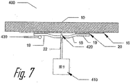
[0046]試験試料は、電力およびアンテナコネクター18、30が合金IIおよび合金IVではんだ付けされているフロントガラスであった。図7に例示するこの試験400では、気候制御チャンバーの温度を96時間にわたり105℃で保持し、1時間おきに15分間にわたり14Vでの電流負荷を電力ライン22を介して施用した。電力コネクター18を、はんだ層20およびリヤウィンドウ10に概して垂直な方向で、96時間全体の間に重力加速度として垂直に下方に方向付けられた10ニュートンの機械的負荷(はんだパッド19の間のほぼ中間点に置かれたフック420により重り410を電力コネクター18に接続することにより施用される)に付した。アンテナコネクター30を、同様に3ニュートンの機械的負荷に付した。96時間の試験の後、各電力コネクター18を、図6に示し上記したように、デジタルフォースゲージ(Mark−10 Long Island,ニューヨーク州,モデルBG50)で280〜360ニュートンの力まで3秒間引っ張った(周囲温度において)。この試験の間に、電力コネクター18の不具合は生じなかった。アンテナコネクター18を同様に30〜70ニュートンの力で試験した。合金IVではんだ付けした18個のアンテナコネクター18のうち10個に不具合が生じた。
III.高温保管試験
[0047]試験試料は、電力およびアンテナコネクター30、18が合金IIおよび合金IVではんだ付けされているフロントガラスであった。この試験では、気候制御チャンバーの温度(比較的乾いた湿度においてであるが、制御されていない)を120℃一定で24時間維持し、電力コネクター18に電気的または機械的負荷はかけなかった。24時間終了後、各電力コネクター18を、図6に示し上記したように、デジタルフォースゲージで210〜290ニュートンの力まで3秒間引っ張った(周囲温度において)。アンテナコネクター30は、各アンテナコネクター18を50〜75ニュートンの力で引っ張ることにより同様に試験した。この試験の間に電力またはアンテナコネクター18、30の不具合は生じなかった。
IV.電気負荷をかけての長期試験
[0048]試験試料は、電力およびアンテナコネクター18、30が合金IIではんだ付けされているフロントガラスであった。この試験では、気候制御チャンバーの温度(湿度は比較的乾いていたが制御されていない)を105℃一定で500時間維持し、500時間全体にわたり14Vでの電流負荷をかけた。500時間終了後、各電力コネクター18を、図6に示し上記したように、デジタルフォースゲージで50ニュートンの力まで3秒間引っ張った(周囲温度において)。この試験の間に不具合は生じなかった。
V.熱衝撃試験
[0049]試験試料は、電力およびアンテナコネクター18、30が合金IVではんだ付けされているフロントガラスであった。この試験において、1サイクルは、電気的または機械的負荷をかけることなく試料を気候制御チャンバーで1時間にわたり105℃に加熱した後、該試料を冷水(約23℃以下、冷蔵庫からのもの)に完全に浸すことからなっていた。各サイクルの後、試料を圧縮空気で乾燥した。5サイクル後およびその後10サイクル後、各電力コネクター18を、図6に示し上記したように、デジタルフォースゲージで17−〜290ニュートンの力まで3秒間引っ張った(周囲温度において)。アンテナコネクター18は、50〜80ニュートンの力まで同様に試験した。この試験の間に不具合は生じなかった。
VI.高湿度試験:一定の気候
[0050]試験試料は、電力およびアンテナコネクター18、30が合金IIではんだ付けされているフロントガラスであった。試料を環境チャンバー内で80℃の一定温度および>96%RHの湿度(蒸気が発生)に合計504時間にわたり暴露し、特定の温度および湿度に達した後10時間目に開始して15分間、その後、504時間の最後まで24時間ごとに15分間、14V(約22Aをもたらす)での電流負荷を電流コネクター18にかけた。504時間終了後、各電力コネクター18を、図6に示し上記したように、デジタルフォースゲージで50ニュートンの力まで3秒間引っ張った(周囲温度において)。この試験の間に不具合は生じなかった。
VII.スクリーンウォッシャー液への耐性
[0051]試験試料は、電力およびアンテナコネクター18、30が合金IIおよび合金IVではんだ付けされているフロントガラスであった。この試験では、電力およびアンテナコネクター18、30を、23℃において、69.5%蒸留水、20%エタノール、10%イソプロパノール、0.5%エチレングリコール、および0.09%ラウリル硫酸ナトリウムで作製された模擬的フロントガラス用ウォッシャー溶液に浸したスポンジで、24時間湿らせた。24時間終了後、各電力コネクター18を、図6に示し上記したように、フォースゲージで70〜310ニュートンの力まで2秒間引っ張った(周囲温度において)。各アンテナコネクター30は、60〜85ニュートンの力まで同様に試験した。この試験の間に不具合は生じなかった。
VII.塩水噴霧試験
[0052]試験試料は、電力およびアンテナコネクター18、30が合金IIではんだ付けされているフロントガラスであった。この試験では、試験試料を試験チャンバー内で塩水噴霧の霧に96時間暴露した。塩水濃度は5%で、pHは6.5〜7.2であった。塩水の霧の温度は+35℃±2℃に設定し、タワー温度は+48℃に設定し、空気圧は16〜18psiであった。96時間終了後、各電力コネクター18を、図6に示し上記したように、50ニュートンの力まで2秒間引っ張った(周囲温度において)。この試験の間に不具合は生じなかった。
[0045] In this test, illustrated in FIG. 5, the temperature of the climate controlled chamber was adjusted from ambient temperature (about 20 ° C.) to −40 ° C. and −40 ° C. for 90 minutes over a total time of 8 hours. Hold, then elevated to 105 ° C. over 120 minutes, then returned to ambient temperature and circulated, starting at the end of the -40 ° C. step and at 105 ° C., as indicated by each arrow in FIG. A current load at 14 V, which ends at the end of the phase, was applied via the
II. Heat soak test
[0046] The test sample was a windshield with power and
III. High temperature storage test
The test sample was a windshield with power and
IV. Long-term test with electrical load
[0048] The test sample was a windshield with power and
V. Thermal shock test
The test sample was a windshield with power and
VI. High humidity test: constant climate
[0050] The test sample was a windshield with power and
VII. Resistance to screen washer fluid
The test sample was a windshield with power and
VII. Salt spray test
[0052] The test sample was a windshield with power and
[0053]本発明のはんだ組成物は、無鉛合金であって、望ましい製造性を提供する一方、より高い使用温度のほか、強度および延性の両方に関する機械的特性、ならびに対象用途に必要な湿潤状態での物理的特性および安定性を達成するものである。望ましい製造性は、製造で生じやすい欠陥または不具合、および銀を含有する金属化電気接点表面のはんだ付けでしばしば起こる銀の滲出(掃去(scavenging))現象を軽減または排除することができるように、十分に低い処理温度を可能にすることを包含する。これは、インジウム−スズ−銀ベースの材料、あるいは、銅、ニッケルおよび鉄、またはアンチモン、銅および亜鉛と一緒に冶金学的に合金化するか、沈殿させるか、分散させることができる、インジウム−スズ−銀ベースの材料によって達成される。 [0053] The solder compositions of the present invention are lead-free alloys that provide desirable manufacturability, while at higher operating temperatures, mechanical properties in terms of both strength and ductility, and the wet state required for the intended application. Achieves physical properties and stability in. The desired manufacturability is such that defects or defects that are likely to occur in manufacturing and the phenomenon of silver scavenging that often occurs when soldering the surface of metallized electrical contacts containing silver can be reduced or eliminated. Includes allowing a sufficiently low processing temperature. It can be metallurgically alloyed, precipitated or dispersed with indium-tin-silver based materials or with copper, nickel and iron, or antimony, copper and zinc, indium-. Achieved by tin-silver based materials.
[0054]本出願で用いる場合、いくつかの態様において、実質的に上記材料からなるはんだ組成物は、特定の材料と、はんだ組成物およびはんだ組成物を包含する電気コネクターの基本的および新規特性に実質的に影響を及ぼさない材料に限定される。はんだ組成物の基本的および新規特性としては、本明細書中に記載する熱的(例えば、液相線および固相線温度)および機械的(例えば、上記性能試験)特性が挙げられる。 [0054] As used in this application, in some embodiments, a solder composition substantially consisting of the above materials is a particular material and the basic and novel properties of the solder composition and the electrical connector comprising the solder composition. Limited to materials that have a substantial effect on. Basic and novel properties of the solder composition include thermal (eg, liquidus and solidus temperature) and mechanical (eg, performance test) properties described herein.
[0055]環境に優しい無鉛材料の提供に加え、本発明のはんだは、自動車用ガラスに用いることができる無鉛はんだの提供、強度および延性の両方に必要な機械的特性の達成、ならびに、望ましい低い製造プロセス温度を保持しつつ、望ましい高い使用温度に耐えることなど、多くの利点を有する。 [0055] In addition to providing an environmentally friendly lead-free material, the solder of the present invention provides lead-free solder that can be used in automotive glass, achieves the mechanical properties required for both strength and ductility, and is desirable low. It has many advantages, such as withstanding the desired high operating temperatures while maintaining the manufacturing process temperature.
[0056]本発明をその好ましい態様に関して記載してきたが、これに限定されることを意図してはおらず、むしろ以下の特許請求の範囲に説明する範囲のみに限定されるものとする。さらに、第1、第2などの用語の使用は、重要度の任意の順位を意味するのではなく、第1、第2などの用語は、1つの要素を他の要素と区別するために用いられる。さらに、1つの(a)、1つの(an)などの使用は、量の限定を意味するのではなく、少なくとも1つの参照事項の存在を意味する。
本発明は以下の態様を含む。
[1]
約40重量%のスズ;
約0.5重量%の銅;
約50重量%のインジウム;
約4.5重量%の銀;
約1.8重量%〜約2.1重量%のニッケル;および
約2.9重量%〜約3.2重量%の鉄;
を含む、はんだとしての使用に適した合金。
[2]
合金が約1.8重量%のニッケルおよび約3.2重量%の鉄を含有する、[1]に記載の合金。
[3]
合金が約2.1重量%のニッケルおよび約2.9重量%の鉄を含有する、[1]に記載の合金。
[4]
合金が約109℃の固相線温度および約115℃の液相線温度を有する、[1]〜[3]のいずれかに記載の合金。
[5]
ガラス部材(10);
ガラス部材(10)上の銀を含有する電気接点表面(16);ならびに
ガラス部材(10)上の電気接点表面(16)に、約40重量%のスズ、約0.5重量%の銅、約50重量%のインジウム;約4.5重量%の銀、約1.8重量%〜約2.1重量%のニッケル、および約2.9重量%〜約3.2重量%の鉄を含む元素混合物を有し、はんだとしての使用に適した合金の層(20)で、はんだ付けされている電気コネクター(18、30);
を含む、ガラス部材(10)上の電気接続部。
[6]
合金が約1.8重量%のニッケルおよび約3.2重量%の鉄を含有する、[5]に記載の電気接続部。
[7]
合金が約2.1重量%のニッケルおよび約2.9重量%の鉄を含有する、[5]に記載の電気接続部。
[8]
合金の重量の約40%を提供するようにスズを加える段階;
合金の重量の約0.5%を提供するように銅を加える段階;
合金の重量の約50%を提供するようにインジウムを加える段階;
合金の重量の約4.5%を提供するように銀を加える段階;
合金の重量の約1.8%〜約2.1%を提供するようにニッケルを加える段階;および
合金の重量の約2.9%〜約3.2%の鉄を提供するように鉄を加える段階;
を含む、はんだとしての使用に適した合金の形成方法。
[9]
ニッケルを加える段階および鉄を加える段階が、合金の重量の約5%を提供するようにニッケル−鉄合金を加えることにより遂行され、該ニッケル−鉄合金が、約36重量%〜約42重量%のニッケルおよび約58重量%〜約64重量%の鉄を含む、[8]に記載の方法。
[10]
約14重量%〜約15重量%のスズ;
約1重量%のアンチモン;
約1重量%の銅;
約5重量%〜約6重量%の銀;
約1重量%〜約3重量%のニッケル;
約1重量の亜鉛;および
約75重量%のインジウム;
を含む、はんだとしての使用に適した合金。
[11]
合金が、約14重量%のスズ、5重量%の銀、および約3重量%のニッケルを含有する、[10]に記載の合金。
[12]
合金が、約15重量%のスズ、6重量%の銀、および約1重量%のニッケルを含有する、[10]に記載の合金。
[13]
合金が約122℃〜約124℃の範囲の固相線温度および約136℃〜約138℃の範囲の液相線温度を有する、[10]〜[12]のいずれかに記載の合金。
[14]
ガラス部材(10);
ガラス部材(10)上の銀を含有する電気接点表面(16);ならびに
ガラス部材(10)上の電気接点表面(16)に、約14重量%〜約15重量%のスズ、約1重量%のアンチモン、約1重量%の銅、約5重量%〜約6重量%の銀、約1重量%〜約3重量%のニッケル、約1重量%の亜鉛、および約75重量%のインジウムを含む元素混合物を有し、はんだとしての使用に適した合金の層(20)で、はんだ付けされている電気コネクター(18、30);
を含む、ガラス部材上の電気接続部。
[15]
合金が、約14重量%のスズ、5重量%の銀、および約3重量%のニッケルを含有する、[14]に記載の電気接続部。
[16]
合金が約15重量%のスズ、6重量%の銀、および約1重量%のニッケルを含有する、[14]に記載の電気接続部。
[17]
合金の重量の約14%〜約15%を提供するようにスズを加える段階;
合金の重量の約1%を提供するようにアンチモンを加える段階;
合金の重量の約1%を提供するように銅を加える段階;
合金の重量の約5%〜約6%を提供するように銀を加える段階;
合金の重量の約1%〜約3%を提供するようにニッケルを加える段階;
合金の重量の約1%を提供するように亜鉛を加える段階;および
合金の重量の約75%を提供するようにインジウムを加える段階;
を含む、はんだとしての使用に適した合金の形成方法。
[18]
得られる合金が、約14重量%のスズ、5重量%の銀、および約3重量%のニッケルを含有する、[17]に記載の方法。
[19]
得られる合金が、約15重量%のスズ、6重量%の銀、および約1重量%のニッケルを含有する、[17]に記載の方法。
[20]
約75重量%のスズ;
約5重量%の銀;および
約20重量%のインジウム;
を含む、はんだとしての使用に適した合金。
[21]
合金が約177℃の固相線温度を有し、約188℃の液相線温度を有する、[20]に記載の合金。
[22]
ガラス部材(10);
ガラス部材(10)上の銀を含有する電気接点表面(16);ならびに
ガラス部材(10)上の電気接点表面(16)に、約75重量%のスズ、約5重量%の銀、および約20重量%のインジウムを含む元素混合物を有し、はんだとしての使用に適した合金の層(20)で、はんだ付けされている電気コネクター(18、30);
を含む、ガラス部材上の電気接続部。
[23]
合金の重量の約75%を提供するようにスズを加える段階;
合金の重量の約5%を提供するように銀を加える段階;および
合金の重量の約20%を提供するようにインジウムを加える段階;
を含む、はんだとしての使用に適した合金の形成方法。
[24]
約7重量%のスズ;
約3重量%の銀;および
約90重量%のインジウム;
を含む、はんだとしての使用に適した合金。
[25]
合金が約135℃の固相線温度および約140℃の液相線温度を有する、[24]に記載の合金。
[26]
ガラス部材(10);
ガラス部材(10)上の銀を含有する電気接点表面(16);ならびに
ガラス部材(10)上の電気接点表面(16)に、約7重量%のスズ、約3重量%の銀、および約90重量%のインジウムを含む元素混合物を有し、はんだとしての使用に適した合金の層(20)で、はんだ付けされている電気コネクター(18、30);
を含む、ガラス部材上の電気接続部。
[27]
合金の重量の約7%を提供するようにスズを加える段階;
合金の重量の約3%を提供するように銀を加える段階;および
合金の重量の約90%を提供するようにインジウムを加える段階;
を含む、はんだとしての使用に適した合金の形成方法。
Although the present invention has been described with respect to its preferred embodiments, it is not intended to be limited thereto, but rather limited to the scope described in the claims below. Furthermore, the use of terms such as 1st and 2nd does not mean any order of importance, but terms such as 1st and 2nd are used to distinguish one element from the other. Be done. Moreover, the use of one (a), one (an), etc. does not mean a limited amount, but the presence of at least one reference.
The present invention includes the following aspects.
[1]
About 40% by weight tin;
About 0.5% by weight copper;
About 50% by weight indium;
About 4.5% by weight silver;
About 1.8% to about 2.1% by weight nickel; and
About 2.9% by weight to about 3.2% by weight of iron;
Alloys suitable for use as solder, including.
[2]
The alloy according to [1], wherein the alloy contains about 1.8% by weight of nickel and about 3.2% by weight of iron.
[3]
The alloy according to [1], wherein the alloy contains about 2.1% by weight nickel and about 2.9% by weight iron.
[4]
The alloy according to any one of [1] to [3], wherein the alloy has a solid phase temperature of about 109 ° C. and a liquidus temperature of about 115 ° C.
[5]
Glass member (10);
Silver-containing electrical contact surface (16) on glass member (10);
On the electrical contact surface (16) on the glass member (10), about 40% by weight tin, about 0.5% by weight copper, about 50% by weight indium; about 4.5% by weight silver, about 1. A layer of alloy having an elemental mixture containing 8% to about 2.1% by weight of nickel and about 2.9% to about 3.2% by weight of iron and suitable for use as a solder (20). And the soldered electrical connectors (18, 30);
An electrical connection on the glass member (10), including.
[6]
The electrical connection according to [5], wherein the alloy contains about 1.8% by weight nickel and about 3.2% by weight iron.
[7]
The electrical connection according to [5], wherein the alloy contains about 2.1% by weight nickel and about 2.9% by weight iron.
[8]
The stage of adding tin to provide about 40% of the weight of the alloy;
The stage of adding copper to provide about 0.5% of the weight of the alloy;
The step of adding indium to provide about 50% of the weight of the alloy;
The stage of adding silver to provide about 4.5% of the weight of the alloy;
The step of adding nickel to provide about 1.8% to about 2.1% of the weight of the alloy; and
The stage of adding iron to provide about 2.9% to about 3.2% of the weight of the alloy;
A method of forming an alloy suitable for use as a solder, including.
[9]
The nickel-iron addition step and the iron addition step are carried out by adding a nickel-iron alloy so as to provide about 5% of the weight of the alloy, the nickel-iron alloy being about 36% by weight to about 42% by weight. The method according to [8], which comprises nickel and about 58% to about 64% by weight of iron.
[10]
About 14% to about 15% tin;
Approximately 1% by weight antimony;
About 1% by weight copper;
About 5% to 6% by weight of silver;
About 1% to about 3% by weight nickel;
About 1 weight of zinc; and
Approximately 75% by weight indium;
Alloys suitable for use as solder, including.
[11]
The alloy according to [10], wherein the alloy contains about 14% by weight tin, 5% by weight silver, and about 3% by weight nickel.
[12]
The alloy according to [10], wherein the alloy contains about 15% by weight tin, 6% by weight silver, and about 1% by weight nickel.
[13]
The alloy according to any one of [10] to [12], wherein the alloy has a solid phase temperature in the range of about 122 ° C to about 124 ° C and a liquidus temperature in the range of about 136 ° C to about 138 ° C.
[14]
Glass member (10);
Silver-containing electrical contact surface (16) on glass member (10);
On the electrical contact surface (16) on the glass member (10), about 14% to about 15% by weight tin, about 1% by weight antimony, about 1% by weight copper, about 5% to about 6% by weight. Layer of alloy having an elemental mixture containing about 1% by weight to about 3% by weight of nickel, about 1% by weight of zinc, and about 75% by weight of indium, suitable for use as a solder (20). And the soldered electrical connectors (18, 30);
Electrical connections on glass members, including.
[15]
The electrical connection according to [14], wherein the alloy contains about 14% by weight tin, 5% by weight silver, and about 3% by weight nickel.
[16]
The electrical connection according to [14], wherein the alloy contains about 15% by weight tin, 6% by weight silver, and about 1% by weight nickel.
[17]
The stage of adding tin to provide about 14% to about 15% of the weight of the alloy;
The stage of adding antimony to provide about 1% of the weight of the alloy;
The stage of adding copper to provide about 1% of the weight of the alloy;
The stage of adding silver to provide about 5% to about 6% of the weight of the alloy;
The stage of adding nickel to provide about 1% to about 3% of the weight of the alloy;
The step of adding zinc to provide about 1% of the weight of the alloy; and
The stage of adding indium to provide about 75% of the weight of the alloy;
A method of forming an alloy suitable for use as a solder, including.
[18]
The method of [17], wherein the alloy obtained contains about 14% by weight tin, 5% by weight silver, and about 3% by weight nickel.
[19]
The method of [17], wherein the alloy obtained contains about 15% by weight tin, 6% by weight silver, and about 1% by weight nickel.
[20]
About 75% by weight tin;
About 5% by weight silver; and
About 20% by weight indium;
Alloys suitable for use as solder, including.
[21]
The alloy according to [20], wherein the alloy has a solid phase temperature of about 177 ° C. and a liquidus temperature of about 188 ° C.
[22]
Glass member (10);
Silver-containing electrical contact surface (16) on glass member (10);
The electrical contact surface (16) on the glass member (10) has an elemental mixture containing about 75% by weight tin, about 5% by weight silver, and about 20% by weight indium, and is suitable for use as a solder. Electrical connectors soldered with a layer of alloy (20) (18, 30);
Electrical connections on glass members, including.
[23]
The stage of adding tin to provide about 75% of the weight of the alloy;
The stage of adding silver to provide about 5% of the weight of the alloy; and
The stage of adding indium to provide about 20% of the weight of the alloy;
A method of forming an alloy suitable for use as a solder, including.
[24]
About 7% by weight tin;
About 3% by weight silver; and
About 90% by weight indium;
Alloys suitable for use as solder, including.
[25]
The alloy according to [24], wherein the alloy has a solid phase temperature of about 135 ° C. and a liquidus temperature of about 140 ° C.
[26]
Glass member (10);
Silver-containing electrical contact surface (16) on glass member (10);
The electrical contact surface (16) on the glass member (10) has an elemental mixture containing about 7% by weight tin, about 3% by weight silver, and about 90% by weight indium, and is suitable for use as a solder. Electrical connectors soldered with a layer of alloy (20) (18, 30);
Electrical connections on glass members, including.
[27]
The stage of adding tin to provide about 7% of the weight of the alloy;
The stage of adding silver to provide about 3% of the weight of the alloy; and
The step of adding indium to provide about 90% of the weight of the alloy;
A method of forming an alloy suitable for use as a solder, including.
10 ガラス部材
12 窓用デフロスター
14 霜取りライン
16 電気接点ストリップ
18 電力コネクター
18a ブリッジ端子電力コネクター
18b ブリッジ端子電力コネクター
19 はんだパッド
20 はんだ組成物の層
22 電力ライン
24 アンテナ
26 アンテナ素子
28 アンテナライン
30 アンテナコネクター
300 引張試験
310 デジタルフォースゲージ
320 フック
330 ハンドル
400 ヒートソーク試験
410 重り
420 フック
10
Claims (4)
2.5〜3.5重量%の銀;および
残部のインジウム;
からなる合金。 6.5-7.5% by weight tin;
2.5-3.5% by weight silver; and
The rest of indium;
Alloy consisting of.
ガラス部材(10)上の銀を含有する電気接点表面(16);ならびに
ガラス部材(10)上の電気接点表面(16)に、6.5〜7.5重量%のスズ、2.5〜3.5重量%の銀、および残部のインジウムからなる元素混合物を有する合金の層(20)で、はんだ付けされている電気コネクター(18、30);
を含む、ガラス部材上の電気接続部。 Glass member (10);
On the silver-containing electrical contact surface (16) on the glass member (10); and on the electrical contact surface (16) on the glass member (10), 6.5-7.5 wt% tin, 2.5- Electrical connectors (18, 30) soldered with a layer of alloy (20) with an elemental mixture of 3.5% by weight silver and the balance of indium;
Electrical connections on glass members, including.
合金の重量の2.5〜3.5%を提供するように銀を加える段階;および
合金の重量の残部を提供するようにインジウムを加える段階;
からなる合金の形成方法。 The step of adding tin to provide 6.5-7.5% of the weight of the alloy;
The step of adding silver to provide 2.5-3.5% of the weight of the alloy; and the step of adding indium to provide the balance of the weight of the alloy;
A method of forming an alloy consisting of.
Applications Claiming Priority (5)
| Application Number | Priority Date | Filing Date | Title |
|---|---|---|---|
| US201562161966P | 2015-05-15 | 2015-05-15 | |
| US62/161,966 | 2015-05-15 | ||
| US201562168054P | 2015-05-29 | 2015-05-29 | |
| US62/168,054 | 2015-05-29 | ||
| PCT/US2016/032076 WO2016186954A1 (en) | 2015-05-15 | 2016-05-12 | Indium-tin-silver based lead free solder |
Related Child Applications (1)
| Application Number | Title | Priority Date | Filing Date |
|---|---|---|---|
| JP2020083093A Division JP7082641B2 (en) | 2015-05-15 | 2020-05-11 | Indium-tin-silver-based lead-free solder |
Publications (3)
| Publication Number | Publication Date |
|---|---|
| JP2018520005A JP2018520005A (en) | 2018-07-26 |
| JP2018520005A5 JP2018520005A5 (en) | 2019-03-22 |
| JP6826995B2 true JP6826995B2 (en) | 2021-02-10 |
Family
ID=57320312
Family Applications (2)
| Application Number | Title | Priority Date | Filing Date |
|---|---|---|---|
| JP2017557925A Active JP6826995B2 (en) | 2015-05-15 | 2016-05-12 | Indium-tin-silver-based lead-free solder |
| JP2020083093A Active JP7082641B2 (en) | 2015-05-15 | 2020-05-11 | Indium-tin-silver-based lead-free solder |
Family Applications After (1)
| Application Number | Title | Priority Date | Filing Date |
|---|---|---|---|
| JP2020083093A Active JP7082641B2 (en) | 2015-05-15 | 2020-05-11 | Indium-tin-silver-based lead-free solder |
Country Status (7)
| Country | Link |
|---|---|
| US (1) | US9981347B2 (en) |
| EP (1) | EP3294489A4 (en) |
| JP (2) | JP6826995B2 (en) |
| KR (1) | KR102272298B1 (en) |
| CN (4) | CN115139008B (en) |
| TW (1) | TWI652354B (en) |
| WO (1) | WO2016186954A1 (en) |
Families Citing this family (10)
| Publication number | Priority date | Publication date | Assignee | Title |
|---|---|---|---|---|
| HUE054283T2 (en) * | 2015-05-05 | 2021-08-30 | Saint Gobain | Pane with electric connection element and connecting element attached thereto |
| GB201515010D0 (en) * | 2015-08-24 | 2015-10-07 | Pilkington Group Ltd | Electrical connector |
| JP7239835B2 (en) | 2017-11-07 | 2023-03-15 | セントラル硝子株式会社 | Vehicle window glass assembly |
| CN112638575A (en) * | 2018-09-07 | 2021-04-09 | 中央硝子株式会社 | Glazing assembly for vehicle windows |
| CN109648222A (en) * | 2019-01-21 | 2019-04-19 | 上海莜玮汽车零部件有限公司 | A kind of leadless welding alloy and its application |
| CN109702372A (en) * | 2019-03-06 | 2019-05-03 | 上海莜玮汽车零部件有限公司 | Leadless welding alloy and its application |
| CN109852843A (en) * | 2019-04-02 | 2019-06-07 | 史伟华 | A kind of indium Tin Silver Copper Alloy and its preparation method and application |
| US11383330B2 (en) | 2020-09-21 | 2022-07-12 | Aptiv Technologies Limited | Lead-free solder composition |
| CN113042842A (en) * | 2021-03-24 | 2021-06-29 | 河南东微电子材料有限公司 | Method for welding ruthenium target and back plate |
| CN115041863B (en) * | 2022-06-22 | 2023-04-25 | 浙江亚通新材料股份有限公司 | Composite solder for automobile glass and preparation method and application thereof |
Family Cites Families (24)
| Publication number | Priority date | Publication date | Assignee | Title |
|---|---|---|---|---|
| JPH0680881B2 (en) * | 1984-06-29 | 1994-10-12 | 富士通株式会社 | Solder melting type high density connector |
| US5256370B1 (en) * | 1992-05-04 | 1996-09-03 | Indium Corp America | Lead-free alloy containing tin silver and indium |
| US5328660A (en) * | 1993-06-16 | 1994-07-12 | International Business Machines Corporation | Lead-free, high temperature, tin based multi-component solder |
| AU6279296A (en) * | 1996-06-12 | 1998-01-07 | International Business Machines Corporation | Lead-free, high tin ternary solder alloy of tin, silver, and indium |
| JP2000141078A (en) * | 1998-09-08 | 2000-05-23 | Nippon Sheet Glass Co Ltd | Leadless solder |
| US6253988B1 (en) | 1999-03-29 | 2001-07-03 | Antaya Technologies Corporation | Low temperature solder |
| US6689488B2 (en) * | 2001-02-09 | 2004-02-10 | Taiho Kogyo Co., Ltd. | Lead-free solder and solder joint |
| US20050029666A1 (en) * | 2001-08-31 | 2005-02-10 | Yasutoshi Kurihara | Semiconductor device structural body and electronic device |
| US7111771B2 (en) | 2003-03-31 | 2006-09-26 | Intel Corporation | Solders with surfactant-refined grain sizes, solder bumps made thereof, and methods of making same |
| US20080175748A1 (en) * | 2005-08-12 | 2008-07-24 | John Pereira | Solder Composition |
| US20070037004A1 (en) * | 2005-08-12 | 2007-02-15 | Antaya Technologies Corporation | Multilayer solder article |
| JP2011240352A (en) * | 2010-05-17 | 2011-12-01 | Central Glass Co Ltd | Lead-free solder composition for vehicle |
| JP2011243769A (en) | 2010-05-19 | 2011-12-01 | Tokyo Electron Ltd | Substrate etching method, program and computer storage medium |
| JP5610202B2 (en) | 2010-06-23 | 2014-10-22 | ミネベア株式会社 | Surface lighting device |
| JP2012091216A (en) * | 2010-10-28 | 2012-05-17 | Asahi Glass Co Ltd | Lead-free solder alloy and glass article using the same |
| CN103313886B (en) * | 2011-01-14 | 2015-12-09 | 旭硝子株式会社 | Window glass for vehicle and manufacture method thereof |
| MX356849B (en) * | 2011-02-04 | 2018-06-15 | Antaya Tech Corp | Lead-free solder composition. |
| US9595768B2 (en) * | 2011-05-03 | 2017-03-14 | Pilkington Group Limited | Glazing with a soldered connector |
| JP5861559B2 (en) * | 2012-05-10 | 2016-02-16 | 住友金属鉱山株式会社 | Pb-free In solder alloy |
| MX370004B (en) * | 2012-08-24 | 2019-11-28 | Saint Gobain | Pane having an electrical connection element. |
| KR101821465B1 (en) * | 2012-11-21 | 2018-01-23 | 쌩-고벵 글래스 프랑스 | Disk comprising electric connecting element and connecting bridge |
| CN103341699A (en) * | 2013-07-04 | 2013-10-09 | 浙江亚通焊材有限公司 | Unleaded Sn-In-Ag brazing filler metal replacing tin-lead brazing filler metal |
| JP2016165751A (en) * | 2015-03-10 | 2016-09-15 | 住友金属鉱山株式会社 | Pb-FREE In-BASED SOLDER ALLOY |
| CN104690442A (en) * | 2015-03-17 | 2015-06-10 | 湖南新瑞化工有限公司 | Low-melting-point lead-free solder alloy and preparation method thereof |
-
2016
- 2016-05-12 CN CN202211008509.1A patent/CN115139008B/en active Active
- 2016-05-12 US US15/523,861 patent/US9981347B2/en active Active
- 2016-05-12 CN CN202310564625.XA patent/CN116393868A/en active Pending
- 2016-05-12 CN CN202110190195.0A patent/CN112958943B/en active Active
- 2016-05-12 WO PCT/US2016/032076 patent/WO2016186954A1/en active Application Filing
- 2016-05-12 CN CN201680028036.8A patent/CN107635717B/en active Active
- 2016-05-12 JP JP2017557925A patent/JP6826995B2/en active Active
- 2016-05-12 KR KR1020177022524A patent/KR102272298B1/en active IP Right Grant
- 2016-05-12 EP EP16796973.2A patent/EP3294489A4/en active Pending
-
2017
- 2017-05-10 TW TW106115452A patent/TWI652354B/en not_active IP Right Cessation
-
2020
- 2020-05-11 JP JP2020083093A patent/JP7082641B2/en active Active
Also Published As
| Publication number | Publication date |
|---|---|
| US9981347B2 (en) | 2018-05-29 |
| CN115139008A (en) | 2022-10-04 |
| JP2018520005A (en) | 2018-07-26 |
| US20170368642A1 (en) | 2017-12-28 |
| TWI652354B (en) | 2019-03-01 |
| CN107635717A (en) | 2018-01-26 |
| WO2016186954A1 (en) | 2016-11-24 |
| KR20180006874A (en) | 2018-01-19 |
| CN115139008B (en) | 2023-05-23 |
| EP3294489A1 (en) | 2018-03-21 |
| KR102272298B1 (en) | 2021-07-05 |
| JP2020124747A (en) | 2020-08-20 |
| CN112958943B (en) | 2022-09-06 |
| CN112958943A (en) | 2021-06-15 |
| EP3294489A4 (en) | 2019-04-10 |
| JP7082641B2 (en) | 2022-06-08 |
| CN116393868A (en) | 2023-07-07 |
| TW201807211A (en) | 2018-03-01 |
| CN107635717B (en) | 2021-02-05 |
Similar Documents
| Publication | Publication Date | Title |
|---|---|---|
| JP7082641B2 (en) | Indium-tin-silver-based lead-free solder | |
| JP6928062B2 (en) | Manufacturing method of lead-free solder composition | |
| JP2012091216A (en) | Lead-free solder alloy and glass article using the same | |
| CN108672979B (en) | Lead-free solder alloy, application thereof and glass assembly | |
| US20170266764A1 (en) | Lead free solder composition with high ductility | |
| US20200122278A1 (en) | Lead free solder composition with high ductility | |
| KR20170130757A (en) | Lead free solder composition with high ductility | |
| KR20170133868A (en) | Lead free solder composition with high ductility |
Legal Events
| Date | Code | Title | Description |
|---|---|---|---|
| A521 | Request for written amendment filed |
Free format text: JAPANESE INTERMEDIATE CODE: A523 Effective date: 20190205 |
|
| A621 | Written request for application examination |
Free format text: JAPANESE INTERMEDIATE CODE: A621 Effective date: 20190205 |
|
| A711 | Notification of change in applicant |
Free format text: JAPANESE INTERMEDIATE CODE: A711 Effective date: 20190215 |
|
| RD03 | Notification of appointment of power of attorney |
Free format text: JAPANESE INTERMEDIATE CODE: A7423 Effective date: 20190218 |
|
| RD04 | Notification of resignation of power of attorney |
Free format text: JAPANESE INTERMEDIATE CODE: A7424 Effective date: 20190219 |
|
| A977 | Report on retrieval |
Free format text: JAPANESE INTERMEDIATE CODE: A971007 Effective date: 20191118 |
|
| A131 | Notification of reasons for refusal |
Free format text: JAPANESE INTERMEDIATE CODE: A131 Effective date: 20200106 |
|
| A601 | Written request for extension of time |
Free format text: JAPANESE INTERMEDIATE CODE: A601 Effective date: 20200327 |
|
| A521 | Request for written amendment filed |
Free format text: JAPANESE INTERMEDIATE CODE: A523 Effective date: 20200511 |
|
| A131 | Notification of reasons for refusal |
Free format text: JAPANESE INTERMEDIATE CODE: A131 Effective date: 20201002 |
|
| A521 | Request for written amendment filed |
Free format text: JAPANESE INTERMEDIATE CODE: A523 Effective date: 20201116 |
|
| TRDD | Decision of grant or rejection written | ||
| A01 | Written decision to grant a patent or to grant a registration (utility model) |
Free format text: JAPANESE INTERMEDIATE CODE: A01 Effective date: 20210114 |
|
| A61 | First payment of annual fees (during grant procedure) |
Free format text: JAPANESE INTERMEDIATE CODE: A61 Effective date: 20210118 |
|
| R150 | Certificate of patent or registration of utility model |
Ref document number: 6826995 Country of ref document: JP Free format text: JAPANESE INTERMEDIATE CODE: R150 |
|
| R250 | Receipt of annual fees |
Free format text: JAPANESE INTERMEDIATE CODE: R250 |