JP6826041B2 - Position indicator and position detector - Google Patents
Position indicator and position detector Download PDFInfo
- Publication number
- JP6826041B2 JP6826041B2 JP2017546477A JP2017546477A JP6826041B2 JP 6826041 B2 JP6826041 B2 JP 6826041B2 JP 2017546477 A JP2017546477 A JP 2017546477A JP 2017546477 A JP2017546477 A JP 2017546477A JP 6826041 B2 JP6826041 B2 JP 6826041B2
- Authority
- JP
- Japan
- Prior art keywords
- signal
- light emission
- light emitting
- position detection
- sensor
- Prior art date
- Legal status (The legal status is an assumption and is not a legal conclusion. Google has not performed a legal analysis and makes no representation as to the accuracy of the status listed.)
- Active
Links
Images


Classifications
-
- G—PHYSICS
- G06—COMPUTING OR CALCULATING; COUNTING
- G06F—ELECTRIC DIGITAL DATA PROCESSING
- G06F3/00—Input arrangements for transferring data to be processed into a form capable of being handled by the computer; Output arrangements for transferring data from processing unit to output unit, e.g. interface arrangements
- G06F3/01—Input arrangements or combined input and output arrangements for interaction between user and computer
- G06F3/03—Arrangements for converting the position or the displacement of a member into a coded form
- G06F3/041—Digitisers, e.g. for touch screens or touch pads, characterised by the transducing means
- G06F3/0416—Control or interface arrangements specially adapted for digitisers
- G06F3/04162—Control or interface arrangements specially adapted for digitisers for exchanging data with external devices, e.g. smart pens, via the digitiser sensing hardware
-
- G—PHYSICS
- G01—MEASURING; TESTING
- G01D—MEASURING NOT SPECIALLY ADAPTED FOR A SPECIFIC VARIABLE; ARRANGEMENTS FOR MEASURING TWO OR MORE VARIABLES NOT COVERED IN A SINGLE OTHER SUBCLASS; TARIFF METERING APPARATUS; MEASURING OR TESTING NOT OTHERWISE PROVIDED FOR
- G01D5/00—Mechanical means for transferring the output of a sensing member; Means for converting the output of a sensing member to another variable where the form or nature of the sensing member does not constrain the means for converting; Transducers not specially adapted for a specific variable
- G01D5/12—Mechanical means for transferring the output of a sensing member; Means for converting the output of a sensing member to another variable where the form or nature of the sensing member does not constrain the means for converting; Transducers not specially adapted for a specific variable using electric or magnetic means
- G01D5/14—Mechanical means for transferring the output of a sensing member; Means for converting the output of a sensing member to another variable where the form or nature of the sensing member does not constrain the means for converting; Transducers not specially adapted for a specific variable using electric or magnetic means influencing the magnitude of a current or voltage
- G01D5/20—Mechanical means for transferring the output of a sensing member; Means for converting the output of a sensing member to another variable where the form or nature of the sensing member does not constrain the means for converting; Transducers not specially adapted for a specific variable using electric or magnetic means influencing the magnitude of a current or voltage by varying inductance, e.g. by a movable armature
- G01D5/204—Mechanical means for transferring the output of a sensing member; Means for converting the output of a sensing member to another variable where the form or nature of the sensing member does not constrain the means for converting; Transducers not specially adapted for a specific variable using electric or magnetic means influencing the magnitude of a current or voltage by varying inductance, e.g. by a movable armature by influencing the mutual induction between two or more coils
-
- G—PHYSICS
- G06—COMPUTING OR CALCULATING; COUNTING
- G06F—ELECTRIC DIGITAL DATA PROCESSING
- G06F3/00—Input arrangements for transferring data to be processed into a form capable of being handled by the computer; Output arrangements for transferring data from processing unit to output unit, e.g. interface arrangements
- G06F3/01—Input arrangements or combined input and output arrangements for interaction between user and computer
- G06F3/03—Arrangements for converting the position or the displacement of a member into a coded form
- G06F3/033—Pointing devices displaced or positioned by the user, e.g. mice, trackballs, pens or joysticks; Accessories therefor
- G06F3/0354—Pointing devices displaced or positioned by the user, e.g. mice, trackballs, pens or joysticks; Accessories therefor with detection of two-dimensional [2D] relative movements between the device, or an operating part thereof, and a plane or surface, e.g. 2D mice, trackballs, pens or pucks
- G06F3/03542—Light pens for emitting or receiving light
-
- G—PHYSICS
- G06—COMPUTING OR CALCULATING; COUNTING
- G06F—ELECTRIC DIGITAL DATA PROCESSING
- G06F3/00—Input arrangements for transferring data to be processed into a form capable of being handled by the computer; Output arrangements for transferring data from processing unit to output unit, e.g. interface arrangements
- G06F3/01—Input arrangements or combined input and output arrangements for interaction between user and computer
- G06F3/03—Arrangements for converting the position or the displacement of a member into a coded form
- G06F3/033—Pointing devices displaced or positioned by the user, e.g. mice, trackballs, pens or joysticks; Accessories therefor
- G06F3/0354—Pointing devices displaced or positioned by the user, e.g. mice, trackballs, pens or joysticks; Accessories therefor with detection of two-dimensional [2D] relative movements between the device, or an operating part thereof, and a plane or surface, e.g. 2D mice, trackballs, pens or pucks
- G06F3/03543—Mice or pucks
-
- G—PHYSICS
- G06—COMPUTING OR CALCULATING; COUNTING
- G06F—ELECTRIC DIGITAL DATA PROCESSING
- G06F3/00—Input arrangements for transferring data to be processed into a form capable of being handled by the computer; Output arrangements for transferring data from processing unit to output unit, e.g. interface arrangements
- G06F3/01—Input arrangements or combined input and output arrangements for interaction between user and computer
- G06F3/03—Arrangements for converting the position or the displacement of a member into a coded form
- G06F3/033—Pointing devices displaced or positioned by the user, e.g. mice, trackballs, pens or joysticks; Accessories therefor
- G06F3/0354—Pointing devices displaced or positioned by the user, e.g. mice, trackballs, pens or joysticks; Accessories therefor with detection of two-dimensional [2D] relative movements between the device, or an operating part thereof, and a plane or surface, e.g. 2D mice, trackballs, pens or pucks
- G06F3/03545—Pens or stylus
-
- G—PHYSICS
- G06—COMPUTING OR CALCULATING; COUNTING
- G06F—ELECTRIC DIGITAL DATA PROCESSING
- G06F3/00—Input arrangements for transferring data to be processed into a form capable of being handled by the computer; Output arrangements for transferring data from processing unit to output unit, e.g. interface arrangements
- G06F3/01—Input arrangements or combined input and output arrangements for interaction between user and computer
- G06F3/03—Arrangements for converting the position or the displacement of a member into a coded form
- G06F3/033—Pointing devices displaced or positioned by the user, e.g. mice, trackballs, pens or joysticks; Accessories therefor
- G06F3/038—Control and interface arrangements therefor, e.g. drivers or device-embedded control circuitry
- G06F3/0383—Signal control means within the pointing device
-
- G—PHYSICS
- G06—COMPUTING OR CALCULATING; COUNTING
- G06F—ELECTRIC DIGITAL DATA PROCESSING
- G06F3/00—Input arrangements for transferring data to be processed into a form capable of being handled by the computer; Output arrangements for transferring data from processing unit to output unit, e.g. interface arrangements
- G06F3/01—Input arrangements or combined input and output arrangements for interaction between user and computer
- G06F3/03—Arrangements for converting the position or the displacement of a member into a coded form
- G06F3/041—Digitisers, e.g. for touch screens or touch pads, characterised by the transducing means
- G06F3/046—Digitisers, e.g. for touch screens or touch pads, characterised by the transducing means by electromagnetic means
Landscapes
- Engineering & Computer Science (AREA)
- General Engineering & Computer Science (AREA)
- Theoretical Computer Science (AREA)
- Physics & Mathematics (AREA)
- General Physics & Mathematics (AREA)
- Human Computer Interaction (AREA)
- Electromagnetism (AREA)
- Position Input By Displaying (AREA)
Description
この発明は、電磁誘導方式の位置検出装置及び、この位置検出装置と共に使用される位置指示器に関する。 The present invention relates to an electromagnetic induction type position detector and a position indicator used with the position detector.
位置指示器は、使用者により把持されて、位置検出装置のセンサ上における位置指示のために用いられる。位置検出装置においては、位置指示器と電気的に結合するセンサ電極の位置を検出することで、位置検出装置のセンサ上における位置指示器による指示位置を検出する。このセンサと位置指示器との電気的な結合を検出する方式としては、静電結合を検出する方式、電磁結合を検出する方式、など種々の方式が知られている。 The position indicator is grasped by the user and used for position indication on the sensor of the position detector. In the position detecting device, the position indicated by the position indicator on the sensor of the position detecting device is detected by detecting the position of the sensor electrode that is electrically coupled to the position indicator. As a method for detecting the electrical coupling between the sensor and the position indicator, various methods such as a method for detecting an electrostatic coupling and a method for detecting an electromagnetic coupling are known.
この種の位置指示器において、例えばLED(Light Emitting Diode)からなる発光素子を設け、その発光素子を種々の用途に応じて発光制御するようにすることが従来から行われている。 In this type of position indicator, for example, a light emitting element made of an LED (Light Emitting Diode) is provided, and the light emitting element is controlled to emit light according to various uses.
位置指示器において、発光させる用途としては、
・電源スイッチの操作の確認(例えば特許文献1(特開2011−18090号公報))、
・発光素子をペン先近傍に設けてペン先を照明(例えば特許文献2(特開平11−184633号公報))、
などが知られている。発光素子を発光させることは使用者にとって視認性が高いので、上述のような操作の確認や照明などの用途のほか、その他種々の用途にも用いられている。
In the position indicator, as an application to emit light,
-Confirmation of operation of the power switch (for example, Patent Document 1 (Japanese Unexamined Patent Publication No. 2011-18090)),
A light emitting element is provided near the pen tip to illuminate the pen tip (for example, Patent Document 2 (Japanese Unexamined Patent Publication No. 11-184633)).
Etc. are known. Since it is highly visible to the user to make the light emitting element emit light, it is used not only for the above-mentioned operation confirmation and lighting, but also for various other purposes.
ところで、位置指示器において、発光素子を発光させる電源としては、一般的には、位置指示器に、1次電池を設けたり、2次電池や電気二重層キャパシタなどを設けて、充電器により充電したりする構成とされている。しかし、発光素子の電源として、電池を用いる方法は、電池消耗や充電不足の状態になると、必要な電源電圧が得られないという根本的な問題がある。 By the way, in the position indicator, as a power source for causing the light emitting element to emit light, generally, the position indicator is provided with a primary battery, a secondary battery, an electric double layer capacitor, or the like, and is charged by a charger. It is configured to do. However, the method of using a battery as a power source for a light emitting element has a fundamental problem that a required power source voltage cannot be obtained when the battery is exhausted or insufficiently charged.
この問題を回避する方法として、特許文献1及び特許文献2には、位置指示器に受電用のコイル及び蓄電回路を設けると共に、位置検出装置から電磁波を位置指示器に送ることで、位置指示器は、電磁誘導により電源電圧を発電すること可能であることが記載されている。
As a method of avoiding this problem, in
例えば特許文献3(特開2005−10844号公報)には、位置検出装置のセンサとの位置指示のための結合方式を電磁結合方式とする位置指示器として、コイルとコンデンサとからなる共振回路を備え、位置検出装置のセンサからの交流信号を、この共振回路で受信し、その受信した交流信号を位置指示器から位置検出装置のセンサに帰還することで、位置検出装置で位置指示器による指示位置を検出することができるものが開示されている。そして、この特許文献3の位置指示器においては、位置検出装置からの電磁波をコイルとコンデンサとからなる共振回路で受信し、その受信した信号電力から、当該位置指示器における電源電圧を生成することが開示されている。
For example, in Patent Document 3 (Japanese Unexamined Patent Publication No. 2005-10844), a resonance circuit composed of a coil and a capacitor is provided as a position indicator in which the coupling method for indicating the position of the position detection device with the sensor is an electromagnetic coupling method. By receiving the AC signal from the sensor of the position detection device in this resonant circuit and returning the received AC signal from the position indicator to the sensor of the position detection device, the position detection device gives an instruction by the position indicator. Those capable of detecting the position are disclosed. Then, in the position indicator of
以上のような先行文献の存在により、電源として電池を設けなくても、種々の用途で発光素子を発光させるようにすることができる位置指示器を構成することが可能である。 Due to the existence of the above-mentioned prior documents, it is possible to configure a position indicator capable of causing a light emitting element to emit light for various purposes without providing a battery as a power source.
ところで、位置指示器に発光素子を設けて発光させる用途としては、上述のような位置指示器自身の使い勝手の必要性からのみの用途だけではなく、位置検出装置と位置指示器との連携の上での必要性からの用途もある。例えば、特許文献2には、位置指示器から出力される電磁波を位置検出装置で受信したときに、その位置検出装置から位置指示器に対して発光指示信号を送って、位置指示器で、その発光指示信号に基づいて発光素子を発光させるようにして、位置指示器と位置検出装置とが連携状態にあることを発光素子により使用者に報知するようにすることが記載されている。
By the way, the use of providing a light emitting element in the position indicator to emit light is not limited to the above-mentioned use only due to the necessity of the position indicator itself, but also in cooperation with the position detector and the position indicator. There is also a use from the need in. For example, in
このように、従来、位置検出装置と位置指示器との連携の上での必要性からの用途で、位置指示器において発光素子を発光制御する場合には、上述の特許文献2のように、位置検出装置から位置指示器に発光指示信号などの制御信号を送り、位置指示器は、その発光指示信号などの制御信号を解析して、その解析結果により発光素子を制御するように構成している。すなわち、従来は、位置指示器は、位置検出装置からの信号を受信して発光素子の発光制御を行う制御回路を備えて、発光素子の発光制御を自機で行うようにしている。
As described above, in the conventional case where the light emitting element is controlled to emit light in the position indicator for the purpose of cooperation between the position detection device and the position indicator, as in
したがって、位置指示器においては、従来は、位置検出装置からの信号を受信する受信部と、CPUなどからなる制御回路を備えると共に、その受信部や制御回路、さらに発光素子を発光駆動するのための電源電圧を確保する必要があり、複雑な回路構成を備えなければならず、また、電源の問題もクリアしなければならないという問題があった。 Therefore, in the conventional position indicator, a receiving unit for receiving a signal from the position detecting device and a control circuit including a CPU and the like are provided, and the receiving unit, the control circuit, and the light emitting element are driven to emit light. There is a problem that it is necessary to secure the power supply voltage of the above, a complicated circuit configuration must be provided, and the problem of the power supply must be solved.
この発明は、以上の点に鑑み、簡単な構成の位置指示器により、位置検出装置からの制御により位置指示器に設けた発光素子の発光制御をすることが可能とするようにすることを目的とする。 In view of the above points, it is an object of the present invention to make it possible to control the light emission of the light emitting element provided in the position indicator by the control from the position detection device by the position indicator having a simple configuration. And.
上記の課題を解決するために、この発明は、
発光素子と、
位置検出装置のセンサとの間で信号を送受信するためのコイルと、前記コイルと並列に接続されるコンデンサとを含む共振回路と、
前記共振回路で前記センサから受信した信号の電力を蓄積し、前記蓄積された電力に基づいて前記発光素子を発光駆動制御するための発光駆動制御信号を生成する信号生成回路と、
を備え、
前記位置検出装置のセンサからの信号には、前記センサで位置指示器からの帰還信号として検出するための位置検出用信号と、前記発光素子の発光を制御するための発光制御信号とを含むものであり、前記位置検出装置のセンサは、前記位置検出用信号と前記発光制御信号とを交互に時分割で一定の周期をもって送信する、または、前記位置検出用信号および前記発光制御信号を別々の信号とせずに一つの信号として兼用する信号を送信し、
前記信号生成回路は、前記共振回路で受信された前記位置検出用信号と前記発光制御信号とを含む信号を受けて、発光駆動制御信号を生成し、
前記信号生成回路で生成された前記発光駆動制御信号により前記発光素子が駆動制御されることで、前記位置検出装置による前記発光素子の発光制御がなされる
ことを特徴とする位置指示器を提供する。
In order to solve the above problems, the present invention
Light emitting element and
A resonant circuit including a coil for transmitting and receiving signals to and from the sensor of the position detection device and a capacitor connected in parallel with the coil.
A signal generation circuit that stores the power of the signal received from the sensor in the resonance circuit and generates a light emission drive control signal for controlling the light emission drive of the light emitting element based on the stored power.
With
The signal from the sensor of the position detection device includes a position detection signal for detecting as a feedback signal from the position indicator by the sensor and a light emission control signal for controlling light emission of the light emitting element. The sensor of the position detection device alternately transmits the position detection signal and the light emission control signal at regular intervals in a time division, or separates the position detection signal and the light emission control signal. Send a signal that can be used as a single signal instead of a signal,
The signal generation circuit receives a signal including the position detection signal and the light emission control signal received by the resonance circuit, and generates a light emission drive control signal.
By the signal generating circuit and the light emitting element by the light emission drive control signal generated by it is driven and controlled to provide a position indicator, characterized in that the light emission control of the light emitting element by the position detector is made ..
上述の構成の発明の位置指示器は、コイルとコンデンサとからなる共振回路を備え、その共振回路において、位置検出装置のセンサからの信号を受信する。そして、この発明による位置指示器は、信号生成回路を備え、この信号生成回路で、共振回路が位置検出装置のセンサから受信した信号の電力を蓄積し、蓄積した電力に基づいて、発光素子を発光駆動制御するための発光駆動制御信号を生成する。そして、この発明による位置指示器においては、その生成された発光駆動制御信号により発光素子が発光駆動制御される。 The position indicator of the invention having the above configuration includes a resonance circuit including a coil and a capacitor, and receives a signal from a sensor of the position detection device in the resonance circuit. The position indicator according to the present invention includes a signal generation circuit, in which the resonance circuit stores the power of the signal received from the sensor of the position detection device, and the light emitting element is generated based on the stored power. A light emission drive control signal for controlling light emission drive is generated. Then, in the position indicator according to the present invention, the light emitting element is controlled by the light emitting drive control signal generated.
この発明による位置指示器においては、位置検出装置から受信した信号から、信号生成回路において発光駆動制御信号を生成するだけの簡単な回路を備えるだけで、位置検出装置からの信号により、自位置指示器が備える発光素子を発光駆動制御することができる。この場合に、位置指示器は、発光素子を発光させるためのバッテリーなどの電源を別途設ける必要がないという効果も奏する。 The position indicator according to the present invention is provided with a simple circuit that only generates a light emission drive control signal in the signal generation circuit from the signal received from the position detection device, and the self-position indicator is indicated by the signal from the position detection device. The light emitting element included in the device can be controlled to drive light emission. In this case, the position indicator also has the effect that it is not necessary to separately provide a power source such as a battery for causing the light emitting element to emit light.
また、この発明においては、共振回路は、位置検出装置のセンサから、位置検出用信号と、発光素子の発光制御信号とを含む信号を受信する。そして、信号生成回路は、共振回路が受信した位置検出用信号と発光素子の発光制御信号とを含む信号を受けて、発光駆動制御信号を生成する。すなわち、この発明による位置指示器においては、共振回路で受信したセンサからの信号に含まれる位置検出用信号と発光素子の発光制御信号との両方を受けて、発光制御信号を生成するようにする。したがって、この発明による位置指示器は、信号生成回路は、位置検出用信号と発光素子の発光制御信号とを区別して、発光制御信号のみを抽出して発光駆動制御信号を生成する必要がないので、構成が簡単になる。 Further, in the present invention, the resonance circuit receives a signal including a position detection signal and a light emission control signal of the light emitting element from the sensor of the position detection device. Then, the signal generation circuit receives a signal including the position detection signal received by the resonance circuit and the light emission control signal of the light emitting element, and generates a light emission drive control signal. That is, in the position indicator according to the present invention, the light emission control signal is generated by receiving both the position detection signal included in the signal from the sensor received by the resonance circuit and the light emission control signal of the light emitting element. .. Therefore, in the position indicator according to the present invention, it is not necessary for the signal generation circuit to distinguish between the position detection signal and the light emission control signal of the light emitting element and extract only the light emission control signal to generate the light emission drive control signal. , Easy to configure.
そして、位置検出装置では、発光制御信号を、位置指示器の信号生成回路が、当該発光制御信号の電力を蓄積し、その蓄積された電力に基づいて発光素子を発光駆動制御することができるように生成して、位置指示器の共振回路に供給するだけで良いので、位置検出装置における発光素子の発光制御のための構成も簡単で良いという効果もある。 Then, in the position detection device, the light emission control signal can be controlled by the signal generation circuit of the position indicator by accumulating the electric power of the light emission control signal and controlling the light emitting element by emitting light based on the accumulated electric power. Since it is only necessary to generate the power and supply it to the resonance circuit of the position indicator, there is also an effect that the configuration for controlling the light emission of the light emitting element in the position detection device may be simple.
この発明による位置指示器によれば、位置検出装置から受信した信号から、信号生成回路において発光駆動制御信号を生成するだけの簡単な回路を備えるだけで、位置検出装置からの信号により、自位置指示器が備える発光素子を発光駆動制御することができる。その上、この発明による位置指示器は、発光素子を発光させるためのバッテリーなどの電源を別途設ける必要がないという効果も奏する。 According to the position indicator according to the present invention, it is only provided with a simple circuit for generating a light emission drive control signal in the signal generation circuit from the signal received from the position detection device, and the self-position is based on the signal from the position detection device. The light emitting element included in the indicator can be controlled to drive light emission. In addition, the position indicator according to the present invention also has an effect that it is not necessary to separately provide a power source such as a battery for causing the light emitting element to emit light.
以下、この発明による位置指示器の幾つかの実施形態を、図を参照しながら説明する。 Hereinafter, some embodiments of the position indicator according to the present invention will be described with reference to the drawings.
[第1の実施形態]
この第1の実施形態は、位置指示器が筒状の筐体を備えるペン型の場合の例である。以下の説明では、ペン型の位置指示器は電子ペンと称することとする。
[First Embodiment]
This first embodiment is an example in the case where the position indicator is a pen type having a tubular housing. In the following description, the pen-type position indicator will be referred to as an electronic pen.
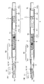
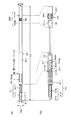
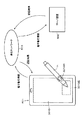
図1は、この発明による位置指示器としての電子ペンの第1の実施形態の構成例を示す図である。この第1の実施形態の電子ペン1は、筒状の筐体2の中空部2a内に、電子ペン本体部を構成する電子ペン用カートリッジ3が収納され、ノックカム機構部4により、電子ペン用カートリッジ3のペン先が、筐体2の長手方向の一端の開口2b側から出し入れされるノック式の構成を備える。
FIG. 1 is a diagram showing a configuration example of a first embodiment of an electronic pen as a position indicator according to the present invention. In the
図1(A)は、電子ペン用カートリッジ3のペン先側(後述する芯体部31のペン先部313の先端)を含め、電子ペン用カートリッジ3の全体が、筐体2の中空部2a内に収容されていて、ペン先が保護されている状態を示している。図1(B)は、ノックカム機構部4により電子ペン用カートリッジ3のペン先の少なくとも先端が、筐体2の開口2bから突出している状態を示している。なお、図1の例では、電子ペン1の筐体2が透明の合成樹脂で構成されているので、その内部が透けて見える状態として示している。
In FIG. 1A, the entire
この実施形態の電子ペン1は、市販のノック式ボールペンと互換性が取れる構成とされている。すなわち、筐体2及び当該筐体2内に設けられるノックカム機構部4は、周知の市販のノック式ボールペンと同一の構成とされると共に、寸法関係も同一に構成される。換言すれば、筐体2及びノックカム機構部4は、市販のノック式のボールペンの筐体及びノックカム機構部をそのまま用いることもできる。そして、電子ペン用カートリッジ3は、後述するように、ボールペンの替え芯6と互換性が取られて、ボールペンの替え芯6(図2(A)参照)の代わりに筐体2内に収納されてノックカム機構部4により、ノック式にペン先が出没可能の構成とされる。
The
ノックカム機構部4は、図1に示すように、カム本体41と、ノック棒42と、回転子43とが組み合わされた周知の構成とされている。カム本体41は、筒状の筐体2の内壁面に形成されている。ノック棒42は、使用者のノック操作を受け付けることができるように、端部42aが、筐体2のペン先側とは反対側の開口2cから突出するようにされている。回転子43は、電子ペン用カートリッジ3のペン先側とは反対側の端部が嵌合される嵌合部43aを備える。
As shown in FIG. 1, the knock
図1(A)の状態において、ノック棒42の端部42aが押下されると、ノックカム機構部4により、電子ペン用カートリッジ3は、筐体2内において図1(B)の状態にロックされ、電子ペン用カートリッジ3のペン先側が、筐体2の開口2bから突出する状態になる。そして、この図1(B)の状態から、ノック棒42の端部42aが再度押下されると、ノックカム機構部4によりロック状態が解除され、復帰用バネ5により、電子ペン用カートリッジ3の筐体2内の位置は、図1(A)の状態に戻る。ノックカム機構部4の詳細な構成及びその動作は、周知であるので、ここでは、その説明を省略する。
When the
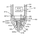
[電子ペン用カートリッジの実施形態]
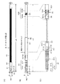
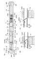
図2は、電子ペン用カートリッジ3の構成例を、市販のノック式ボールペンの替え芯と比較して示す図である。すなわち、図2(A)は、市販のノック式ボールペンの替え芯6を示し、また、図2(B)は、この実施形態の電子ペン用カートリッジ3の構成例を示している。そして、図2(C)は、図2(B)に示すこの実施形態の電子ペン用カートリッジ3の要部の構成を説明するための図である。
[Embodiment of Cartridge for Electronic Pen]
FIG. 2 is a diagram showing a configuration example of the
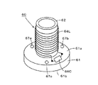
市販のノック式ボールペンの替え芯6は、図2(A)に示すように、ボールが先端に配設されているペン先部61と、インク収納部62とが、結合部63で結合されて一体化された周知の構成を備える。結合部63は、インク収納部62と同じ径を有する。
In the replacement core 6 of a commercially available knock-type ballpoint pen, as shown in FIG. 2A, the
一方、この実施形態の電子ペン用カートリッジ3は、図2(B)に示すように、芯体部31と、筒状体部32とが結合されて一体化された構成を有する。芯体部31は、図2(C)に示すように、磁性体コア、この例ではフェライトコア310に、部分的にコイル311が巻回されていると共に、そのコイル311が巻回されていない部分を保護材312で覆うようにしてペン先部313が形成された構成とされている。
On the other hand, as shown in FIG. 2B, the
この例では、芯体部31においては、コイル311は、フェライトコア310の一方の端部近傍から、フェライトコア310の全長の約1/2長の部分に巻回されている。そして、この例では、フェライトコア310の、コイル311が巻回されていない残りの約1/2長の部分が、例えば樹脂からなる保護材312で覆われてペン先部313とされている。ペン先部313の保護材312としては、比較的硬質で弾性を有する樹脂材料、例えばPOM(Polyoxymethylene)が用いられる。
In this example, in the
この場合に、図2(A)及び図2(B)に示すように、電子ペン用カートリッジ3の芯体部31のペン先部313の径及び長さは、ボールペンの替え芯6のペン先部61の径R1及び長さL1とほぼ等しくなるように構成されている。また、電子ペン用カートリッジ3の芯体部31のコイル311が巻回された部分の径は、ボールペンの替え芯6のインク収納部62の径R2(R2>R1)とほぼ等しくなるように構成されている。
In this case, as shown in FIGS. 2A and 2B, the diameter and length of the
また、筒状体部32は、絶縁性材料例えば樹脂材料で構成されており、電子回路部品が配設される第1の筒状体部321と、筆圧検出用部品が配設される第2の筒状体部322とで構成される。そして、図2(A)及び(B)に示すように、芯体部31と筒状体部32とを結合した状態の長さ(全長)は、ボールペンの替え芯6の全長L2と等しく選定されている。
Further, the
筒状体部32の第1の筒状体部321内には、図2(C)に示すように、プリント基板33が配設されると共に、そのプリント基板33上には、後で詳述するように、コイル311と共に共振回路を構成するコンデンサ341と、発光素子の例としてのLED(Light Emitting Diode;発光ダイオード)342と、このLED342を発光駆動するための発光駆動制御信号を生成する信号生成回路を含む電子回路34(図2(C)では図示を省略。図3参照)が設けられている。
As shown in FIG. 2C, a printed
そして、第1の筒状体部321の側周面には、図2(B)に示すように、LED342の発光光を外部に放出するための光放出部の例としての窓部321Wが形成されている。この窓部321Wは、光透過性であって、かつ、光拡散効果を備える樹脂材料で構成されている。この例では、電子ペン1を把持して使用する使用者はペン先側を注視することを考慮して、窓部321Wは、第1の筒状体部321の芯体部31との結合部に近接する部位に設けられる。そして、LED342は、第1の筒状体部321内のプリント基板33上において、窓部321Wに対応する位置となるように配設されている。
Then, as shown in FIG. 2B, a
なお、窓部321Wは、図2(B)の例では、第1の筒状体部321に1個の矩形状窓部として形成されているように示したが、第1の筒状体部321の外周に沿って、複数個の矩形状窓部をリング状に形成してもよいし、それら複数個の矩形状窓部を連続させたような1個のリング状窓部として形成するようにしてもよい。後述する他の例の窓部についても同様である。
In the example of FIG. 2B, the
そして、芯体部31と、筒状体部32の第1の筒状体部321とは、例えば芯体部31のフェライトコア310の一部が、第1の筒状体部321内に挿入される状態で結合されて一体的に構成される。この場合に、芯体部31と、筒状体部32の第1の筒状体部321との結合に際しては、コイル311の巻き始め端311aと巻き終わり端311bとが、第1の筒状体部321内のプリント基板33上に設けられているコンデンサ341の一端と他端とに電気的に接続されるようにされる(図2(C)参照)。
Then, the
第2の筒状体部322は、この例では、市販のボールペンの替え芯6のインク収納部62の径R2と等しい径の筒状体で構成されている。図2(B)の例では、この第2の筒状体部322は、長尺部322aと、短尺部322bとに2分されており、この例では、その結合部35の近傍に筆圧検出部材36が設けられている。
In this example, the second
すなわち、図2(C)に示すように、この例においては、長尺部322aと短尺部322bとは、結合部35において、連結棒部材351とコイルバネ352を介して結合されている。この場合に、長尺部322aと短尺部322bとは、コイルバネ352により、常に、軸心方向において、互いに離れるように弾性変位されるが、連結棒部材351により、所定位置で係止して、それ以上は軸芯方向に変位しないように構成されている。そして、その係止状態における電子ペン用カートリッジ3の全長が、前述したボールペンの替え芯6の全長L2と等しくなるように構成されている。
That is, as shown in FIG. 2C, in this example, the
そして、図2(C)に示すように、この実施形態では、長尺部322aには、筆圧検出部材36が設けられる。そして、連結棒部材351の一端351a側が、筆圧検出部材36の押圧部として働くように構成されている。
Then, as shown in FIG. 2C, in this embodiment, the pen
この例の筆圧検出部材36は、例えば特許文献:特開2011−186803号公報に記載されている周知の構成の筆圧検出手段を使用した、筆圧に応じて静電容量が変化する可変容量コンデンサの構成とすることができる。なお、筆圧検出部材36は、例えば、特開2013−161307号公報に開示されているような筆圧に応じて静電容量を可変とする半導体素子を用いた構成することもできる。
The pen
この電子ペン用カートリッジ3が筐体2に収納されている状態で、芯体部31に圧力が加わると、電子ペン用カートリッジ3の長尺部322a側の全体が、コイルバネ352の弾性力に抗して、短尺部322b側に移動しようとする力が働き、筆圧検出部材36の静電容量が筆圧に応じたものとなる。
When pressure is applied to the
以上のような構成の電子ペン用カートリッジ3を、その筒状体部32の短尺部322bをノックカム機構部4の回転子43の嵌合部43aに嵌合させることにより、筐体2内に収納する。この状態では、電子ペン用カートリッジ3の芯体部31を含めて、その全体が筐体2内に収納されて、電子ペン用カートリッジ3の芯体部31が保護される。
The
そして、この実施形態の電子ペン1においては、使用者は、位置検出装置と共に使用するときには、ノック棒42の端部42aを押下することで、図1(B)に示すように、芯体部31のペン先部313の先端を筐体2の開口2bから突出させるようにする。これにより、電子ペン用カートリッジ3の芯体部31の保護が解除される。そして、電子ペン1の使用が終了したら、ノック棒42の端部42aを再押下することで、図1(A)に示すように、電子ペン用カートリッジ3の全体を筐体2の中空部2a内に収容するようにして、芯体部31を保護するようにする。
Then, in the
[電子ペン1の回路構成及び電子ペン1と共に使用される位置検出装置の回路構成]
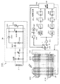
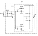
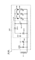
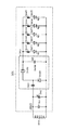
図3は、電子ペン1の電子回路34の回路構成例と、この電子ペン1と電磁誘導結合による信号授受を行う位置検出装置200の回路構成例を示すものである。
[Circuit configuration of
FIG. 3 shows a circuit configuration example of the
電子ペン1は、この実施形態では、位置検出装置200のセンサの導体と電磁誘導結合することにより、位置検出装置200のセンサからの位置検出用信号及び発光制御信号を受信すると共に、受信した位置検出用信号に筆圧検出部材36を通じて検出される筆圧情報を反映させた信号を、位置検出装置200のセンサに送信して帰還するように構成されている。
In this embodiment, the
すなわち、電子ペン用カートリッジ3の電子回路34においては、コイル311に対して、コンデンサ341が並列に接続されると共に、筆圧検出部材36で構成される可変容量コンデンサ36Cが並列に接続されて共振回路340Rが構成される。
That is, in the
一方、位置検出装置200には、図3に示すように、X軸方向ループコイル群211Xと、Y軸方向ループコイル群212Yとが位置検出コイルとして積層されたセンサ210が設けられている。センサ210の各ループコイル群211X,212Yは、例えば、それぞれn,m本の矩形のループコイルからなっている。各ループコイル群211X,212Yを構成する各ループコイルは、等間隔に並んで順次重なり合うように配置されている。
On the other hand, as shown in FIG. 3, the position detection device 200 is provided with a
センサ210のループコイル群211X,212Yは、電子ペン用カートリッジ3の電子回路34の共振回路340Rと電磁結合して、信号の授受を行うことが可能である。この実施形態では、後述するように、位置検出装置200は、センサ210から、位置指示器1に対して位置検出用信号と、LED342の発光制御信号を含む信号を送出する。センサ210から送出される信号は、所定周波数f0の交流信号とされている。
The
電子ペン1の共振回路340Rは、位置検出装置200のセンサ210からの交流信号を電磁結合により受信すると共に、受信した交流信号を位置検出装置200のセンサ210に帰還するように動作する。ただし、共振回路340Rは、筆圧検出部材36で構成される可変容量コンデンサ36Cを含んでいるために、筆圧検出部材36で筆圧が検出されたときには、その可変容量コンデンサ36Cの静電容量の変化に応じた共振周波数(位相)を呈する。このため、共振回路340Rから位置検出装置200のセンサ210に帰還される信号は、当該共振回路340Rの共振周波数の変化分(位相変化分)の情報を含んだものとなっている。位置検出装置200では、後述するように、共振回路340Rから受信した信号に含まれる共振周波数の変化分(位相変化分)の情報を検出することで、筆圧検出部材36で検出された筆圧の情報を検出する。
The
そして、電子ペン用カートリッジ3の電子回路34においては、共振回路340Rに対して信号生成回路343が接続されると共に、信号生成回路343に対して発光素子の例としてのLED342が接続されている。信号生成回路343は、共振回路340Rがセンサ210から受信した信号の電力を蓄積し、その蓄積した電力に基づいて発光素子を発光駆動制御するための発光駆動制御信号(発光駆動制御電圧ED)を生成する。
In the
図3に示すように、この実施形態では、信号生成回路343は、半波2倍圧整流回路の構成であり、コンデンサ3431及び3434と、整流用のダイオード3432及び3433とを備えている。すなわち、共振回路340Rを構成するコイル311の一端がコンデンサ3431を介してダイオード3432のカソードに接続され、ダイオード3432のアノードがコイル311の他端に接続されている。そして、コンデンサ3431とダイオード3432のカソードとの接続点が、ダイオード3433のアノードに接続され、このダイオード3433のカソードがコンデンサ3434を介して、コイル311の他端に接続されている。そして、LED342は、信号生成回路343のコンデンサ3434の一端及び他端間に接続されている。
As shown in FIG. 3, in this embodiment, the
信号生成回路343は、以上のような構成により、共振回路340Rで受信したセンサ210からの交流信号をダイオード3432及び3433で整流して、その整流電流によりコンデンサ3434を充電して、センサ210からの交流信号の電力をコンデンサ3434に蓄積する。そして、この実施形態では、そのコンデンサ3434の両端間に得られる電圧を、発光駆動制御電圧EDとして、LED342に供給するようにする。
With the above configuration, the
したがって、LED342は、コンデンサ3434の両端間電圧である発光駆動制御電圧EDが、所定値以上になると、その発光を開始し、当該発光駆動制御電圧EDの値が所定値よりもさらに大きくなれば、その大きさに応じた強度で発光するようになる。
Therefore, the
次に、位置検出装置200側の構成について説明する。図3に示すように、位置検出装置200には、センサ210を構成するX軸方向ループコイル群211X及びY軸方向ループコイル群212Yが接続される選択回路213が設けられている。この選択回路213は、2つのループコイル群211X,212Yのうちの一のループコイルを順次選択する。
Next, the configuration on the position detection device 200 side will be described. As shown in FIG. 3, the position detection device 200 is provided with a
さらに、位置検出装置200には、発振器221と、電流ドライバ222と、切り替え接続回路223と、受信アンプ224と、検波器225と、ローパスフィルタ226と、サンプルホールド回路227と、A/D変換回路228と、同期検波器229と、ローパスフィルタ230と、サンプルホールド回路231と、A/D変換回路232と、処理制御部233とが設けられている。処理制御部233は、例えばマイクロコンピュータにより構成されている。
Further, the position detection device 200 includes an
発振器221は、周波数f0の交流信号を発生する。そして、発振器221は、発生した交流信号を、電流ドライバ222と同期検波器229に供給する。電流ドライバ222は、発振器221から供給された交流信号を電流に変換して切り替え接続回路223へ送出する。電流ドライバ222は、処理制御部233からの制御信号を受けて、そのゲインを制御する。これにより、電流ドライバ222から出力される交流信号の振幅は、処理制御部233からの制御信号に応じた大きさとなるように制御される。
The
切り替え接続回路223は、後述する処理制御部233からの制御により、選択回路213によって選択されたループコイルが接続される接続先(送信側端子T、受信側端子R)を切り替える。この接続先のうち、送信側端子Tには電流ドライバ222が、受信側端子Rには受信アンプ224が、それぞれ接続されている。
The
切り替え接続回路223が送信側端子Tに接続されているときには、選択回路213により選択されたループコイルに発振器221からの交流信号が電流ドライバ222を通じて流れることによりセンサ210からは電磁界が発生する。電子ペン1がセンサ210の近傍に存在する場合には、その電磁界により共振回路340Rに誘導電流が発生して、共振回路340Rが、センサ210からの周波数f0の交流信号を受信する。
When the
そして、切り替え接続回路223が送信側端子Tから受信側端子Rに切り替えられると、電子ペン1の共振回路340Rは、センサ210から受信した交流信号を、センサ210に帰還するように動作する。このとき、前述したように、共振回路340Rの共振周波数は、前記周波数f0よりも、筆圧検出部材36からなる可変容量コンデンサ36Cの静電容量に応じた分だけ変化したものとなっている。
Then, when the
センサ210においては、電子ペン1の近傍のループコイルに、帰還した信号に応じた誘導電圧が発生する。このループコイルに発生する誘導電圧は、選択回路213が当該ループコイルを選択している状態の時に位置検出装置200で検出することができる。そして、選択回路213により選択されたループコイルに発生する誘導電圧は、選択回路213及び切り替え接続回路223の受信側端子Rを介して受信アンプ224に送られる。受信アンプ224は、ループコイルから供給された誘導電圧を増幅し、検波器225及び同期検波器229へ送出する。
In the
検波器225は、ループコイルに発生した誘導電圧、すなわち受信信号を検波し、ローパスフィルタ226へ送出する。ローパスフィルタ226は、前述した周波数f0より充分低い遮断周波数を有しており、検波器225の出力信号を直流信号に変換してサンプルホールド回路227へ送出する。サンプルホールド回路227は、ローパスフィルタ226の出力信号の所定のタイミング、具体的には受信期間中の所定のタイミングにおける電圧値を保持し、A/D(Analog to Digital)変換回路228へ送出する。A/D変換回路228は、サンプルホールド回路227のアナログ出力をディジタル信号に変換し、処理制御部233に出力する。
The
一方、同期検波器229は、受信アンプ224の出力信号を発振器221からの交流信号で同期検波し、それらの間の位相差に応じたレベルの信号をローパスフィルタ230に送出する。このローパスフィルタ230は、周波数f0より充分低い遮断周波数を有しており、同期検波器229の出力信号を直流信号に変換してサンプルホールド回路231に送出する。このサンプルホールド回路231は、ローパスフィルタ230の出力信号の所定のタイミングにおける電圧値を保持し、A/D(Analog to Digital)変換回路232へ送出する。A/D変換回路232は、サンプルホールド回路231のアナログ出力をディジタル信号に変換し、処理制御部233に出力する。
On the other hand, the
処理制御部233は、位置検出装置200の各部を制御する。すなわち、処理制御部233は、選択回路213におけるループコイルの選択、切り替え接続回路223の切り替え、サンプルホールド回路227、231のタイミングを制御する。処理制御部233は、A/D変換回路228、232からの入力信号に基づき、X軸方向ループコイル群211X及びY軸方向ループコイル群212Yから一定の送信継続時間をもって電波を送信させる。
The
X軸方向ループコイル群211X及びY軸方向ループコイル群212Yの各ループコイルには、前述したように、電子ペン1から送信される電波によって誘導電圧が発生する。処理制御部233は、この各ループコイルに発生した誘導電圧の電圧値のレベルに基づいて電子ペン1によるX軸方向及びY軸方向の指示位置の座標値を算出する。また、処理制御部233は、送信した電波と受信した電波との位相差に応じた信号のレベルに基づいて電子ペン1の芯体に印加されている筆圧を検出する。
As described above, an induced voltage is generated in each of the loop coils of the X-axis direction
このようにして、位置検出装置200では、接近した電子ペン1の位置を処理制御部233で検出することができる。しかも、受信した信号の位相を検出することにより、電子ペン1の筆圧値の情報を得ることができる。
In this way, in the position detection device 200, the position of the approaching
[位置検出装置200及び電子ペン1の動作シーケンス例]
以下に、位置検出装置200での電子ペン1による指示位置の検出動作及び位置検出装置200からの発光制御信号による電子ペン1におけるLED342の発光制御動作について説明する。
[Example of operation sequence of position detection device 200 and electronic pen 1]
Hereinafter, the operation of detecting the indicated position by the
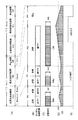
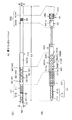
図4は、位置検出装置200及び電子ペン1の動作シーケンス例を説明するためのタイミングチャートを示すものである。この実施形態においては、位置検出装置200の処理制御部233は、図4(A)に示すように、一定の周期Tで、位置検出動作及び電子ペン1のLED342の発光制御処理動作を繰り返すように処理制御する。
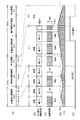
FIG. 4 shows a timing chart for explaining an operation sequence example of the position detection device 200 and the
1周期Tは、位置検出用期間PXYと、発光制御用期間PDと、休止期間PPとからなり、例えば、周期T=7.5ミリ秒、位置検出用期間PXY=3ミリ秒、発光制御用期間PD=3ミリ秒、休止期間PP=1.5ミリ秒とされている。位置検出用期間PXYは、前半の1.5ミリ秒のX座標位置検出用期間PXと、後半の1.5ミリ秒のY座標位置検出用期間PYとに2分されている。 One cycle T is composed of a position detection period PXY, a light emission control period PD, and a rest period PP. For example, a cycle T = 7.5 ms, a position detection period PXY = 3 ms, and a light emission control. The period PD = 3 ms and the rest period PP = 1.5 ms. The position detection period PXY is divided into two, a first half 1.5 milliseconds X coordinate position detection period PX and a second half 1.5 milliseconds Y coordinate position detection period PY.
そして、位置検出装置200においては、X座標位置検出用期間PXの前半の期間では、処理制御部233により、切り替え接続回路223が、図4(B)に示すように、送信側端子Tに切り替えられると共に、選択回路213が、X軸方向ループコイル群211Xの各ループコイルを順次に選択するように制御される。
Then, in the position detection device 200, in the first half of the X coordinate position detection period PX, the
したがって、位置検出装置200においては、発振器221からの、周波数がf0であって、電流ドライバ222を通じて所定の振幅M1とされている交流信号が、X座標位置検出用期間PXの前半の期間の全体に亘る信号連続時間において、図4(C)に示すように、X座標検出用の位置検出用信号SBxとしてセンサ210に供給される。このとき、センサ210においては、X軸方向ループコイル群211Xの各ループコイルが、処理制御部233により選択回路213において順次に選択制御されるので、位置検出用信号SBxは、X軸方向ループコイル群211Xの各ループコイルに順次に供給される。センサ210から電子ペン1に対する信号としては、この位置検出用信号SBxは、図4(C)に示すようなバースト状信号となっている。
Therefore, in the position detection device 200, the AC signal from the
X座標位置検出用期間PXの後半の期間になると、処理制御部233により、切り替え接続回路223が、図4(B)に示すように、受信側端子Rに切り替えられると共に、選択回路213が、X軸方向ループコイル群211Xの各ループコイルを順次に選択するように制御される。このとき、位置検出装置200のセンサ210のX軸方向ループコイル群211Xの各ループコイルは、位置検出用信号SBxを受信した電子ペン1の共振回路340Rからの帰還信号を受信することができる状態となる。そして、処理制御部233により選択回路213が選択制御されることにより、X軸方向ループコイル群211Xの各ループコイルに誘起される電圧が、切り替え接続回路223を通じて受信アンプ224に供給される。
In the latter half of the X coordinate position detection period PX, the
受信アンプ224に供給された信号は、前述したようにして処理され、処理制御部233は、X軸方向ループコイル群211Xの各ループコイルの誘起電圧のレべルを検出する。この場合に、電子ペン1がセンサ210上の近傍に無いときには、処理制御部233は、X軸方向ループコイル群211Xのいずれのループコイルからも、所定レべル以上の誘起電圧を検出しない。
The signal supplied to the receiving
そして、電子ペン1がセンサ210上の近傍に持ち来たらされると、電子ペン1の近傍のループコイルに誘起される帰還信号のレベルが所定値以上になる。位置検出装置200の処理制御部233は、このX座標位置検出用期間PXの受信期間において、X軸方向ループコイル群211Xの各ループコイルの誘起電圧をチェックして、レベルが所定値以上となっているものが検出されたかどうかを監視する。そして、処理制御部233は、レベルが所定値以上となっているループコイルを検出すると、電子ペン1が位置検出装置200のセンサ210上に持ち来たらされていて、電子ペン1の共振回路340Rと位置検出装置200とが電磁結合する状態にあると判断する。この状態は、電子ペン1が位置検出装置200のセンサ210に対して位置指示を行える状態となる。
Then, when the
そして、電子ペン1の共振回路340Rと位置検出装置200とが電磁結合する状態にあるときには、処理制御部233は、X軸方向ループコイル群211Xの各ループコイルの誘起電圧に基づいて、電子ペン1のセンサ210上におけるX座標位置を検出すると共に、検出した誘起電圧の周波数変位(位相変位)から、電子ペン1に印加されている筆圧を検出するようにする。
Then, when the
次に、Y座標位置検出用期間PYでは、同様にして、処理制御部233により、切り替え接続回路223が、図4(B)に示すように、Y座標位置検出用期間PYの前半の期間では送信側端子Tに切り替えられ、後半の期間では受信側端子Rに切り替えられる。また、処理制御部233により、Y座標位置検出用期間PYの前半の期間及び後半の期間のそれぞれにおいて、選択回路213が、Y軸方向ループコイル群212Yの各ループコイルを順次に選択するように制御される。
Next, in the Y coordinate position detection period PY, similarly, by the
そして、位置検出装置200においては、X座標位置検出用期間PXと同様にして、Y座標位置検出用期間PYにおいても、前半の期間では、図4(C)に示すように、発振器221からの、周波数がf0であって、電流ドライバを通じて所定の振幅M1とされている交流信号が、Y座標検出用の位置検出用信号SByとしてセンサ210のY軸方向ループコイル群212Yの各ループコイルに順次に供給される。センサ210から電子ペン1に対する信号としては、この位置検出用信号SByは、図4(C)に示すようなバースト状信号となっている。
Then, in the position detection device 200, in the same manner as the X coordinate position detection period PX, in the Y coordinate position detection period PY, in the first half period, as shown in FIG. 4C, the
Y座標位置検出用期間PYの後半の期間になると、位置検出装置200のセンサ210のY軸方向ループコイル群212Yの各ループコイルは、位置検出用信号SByを受信した電子ペン1の共振回路340Rからの帰還信号を受信することができる状態となる。そして、処理制御部233により選択回路213が選択制御されることにより、Y軸方向ループコイル群212Yの各ループコイルに誘起される電圧が、切り替え接続回路223を通じてアンプ224に供給される。
In the latter half of the Y coordinate position detection period PY, each loop coil of the Y-axis direction
そして、処理制御部233は、X座標位置検出用期間PXの後半の期間と前述と同様にして、Y軸方向ループコイル群212Yの各ループコイルの誘起電圧のレべルを監視することで、電子ペン1の共振回路340Rと位置検出装置200とが電磁結合する状態にあると判断すると共に、電子ペン1の共振回路340Rと位置検出装置200とが電磁結合する状態にあると判断したときには、Y軸方向ループコイル群212Yの各ループコイルの誘起電圧に基づいて、電子ペン1のセンサ210上におけるY座標位置を検出すると共に、検出した誘起電圧の周波数変位(位相変位)から、電子ペン1に印加されている筆圧を検出するようにする。
Then, the
次に、位置検出用期間PXYに続く発光制御用期間PDにおいては、処理制御部233により、切り替え接続回路223が、図4(B)に示すように、送信側端子Tに切り替えられると共に、選択回路213が、X軸方向ループコイル群211Xの各ループコイルを順次に選択するように制御される。
Next, in the light emission control period PD following the position detection period PXY, the
したがって、位置検出装置200においては、図4(C)に示すように、発振器221からの、周波数がf0であって、電流ドライバ222を通じて処理制御部233の制御に応じた所定の振幅M2とされている交流信号が、発光制御用期間の全体に亘る信号連続時間において、発光制御信号LBとして、センサ210に供給される。このとき、センサ210においては、X軸方向ループコイル群211X及び/またはY軸方向ループコイル群212Yの各ループコイルが、処理制御部233により選択回路213において順次に選択制御される。したがって、発光制御信号LBは、X軸方向ループコイル群211X及び/またはY軸方向ループコイル群212Yの各ループコイルに順次に供給されるが、センサ210から電子ペン1に対する信号としては、この発光制御信号LBは、図4(C)に示すようなバースト状信号となっている。
Therefore, in the position detection device 200, as shown in FIG. 4C, the frequency from the
発光制御用期間PDに続く休止期間PPにおいては、切り替え接続回路223は、端子T及び端子Rのいずれにも接続しない状態にする。あるいは、切り替え接続回路223は、端子R側に接続しておくようにしてもよいし、ただし、端子R側に接続しておく場合には、処理制御部233は、受信時の動作は行わないようにする。これにより、位置検出装置200は、送信及び受信の処理において休止期間PPとなる。
In the pause period PP following the light emission control period PD, the
図4の例では、位置検出用信号SBの振幅M1と発光制御信号LBの振幅M2とは、等しくされている。そして、位置検出用信号SBと発光制御信号LBとでは、バースト状信号の信号連続時間が、位置検出用信号SBのそれが0.75ミリ秒の短時間であるのに対して、発光制御信号LBのそれが3ミリ秒と、位置検出用信号SBよりも長時間となっている点が異なる。 In the example of FIG. 4, the amplitude M1 of the position detection signal SB and the amplitude M2 of the light emission control signal LB are equal to each other. In the position detection signal SB and the light emission control signal LB, the signal continuous time of the burst-like signal is a short time of 0.75 milliseconds for the position detection signal SB, whereas the light emission control signal. The difference is that the LB has 3 milliseconds, which is longer than the position detection signal SB.
発光制御信号LBが、位置検出用信号SBよりも信号連続時間が長いことにより、この実施形態では、電子ペン1が位置検出装置200のセンサ210上の近傍に持ち来たらされると、電子ペン1の発光素子としてのLED342が、位置検出装置200のセンサ210からの発光制御信号LBにより、発光駆動される。
Since the light emission control signal LB has a longer signal continuous time than the position detection signal SB, in this embodiment, when the
すなわち、電子ペン1の電子回路34においては、図3に示すように、共振回路340Rで位置検出装置200のセンサ210からの信号を電磁結合により受け、そして、受けた信号をセンサ210に帰還するようにする。
That is, in the
そして、このとき、共振回路340Rで受信されたセンサ210からの交流信号は、信号生成回路343の整流用ダイオード3432及び3433を通じてコンデンサ3434に蓄積される。コンデンサ3434の両端間電圧である発光駆動制御電圧EDは、図4(D)に示すように、発光制御信号LBとしてのバースト状信号が存在している間は、蓄積動作(充電動作)により上昇し、バースト状信号が無くなると、放電動作により低下する。
At this time, the AC signal from the
このため、信号連続時間が短い位置検出用信号SBによっては、コンデンサ3434の両端間に得られる発光駆動制御電圧EDは、LED342を発光させる駆動電圧の閾値Ethを超えることはない。一方、電子ペン1が、位置検出用信号SBよりも信号連続時間が長い発光制御信号LBを受信すると、図4(D)に示すように、コンデンサ3434の両端間電圧である発光駆動制御電圧EDは、LED342を発光させる駆動電圧の閾値Ethを超える。これにより、LED342は、発光駆動される状態(LED点灯状態)になる(図4(E)参照)。
Therefore, depending on the position detection signal SB having a short signal continuous time, the light emission drive control voltage ED obtained between both ends of the
したがって、電子ペン1が位置検出装置200のセンサ210上の近傍に位置するようになると、図4(D)に示すように、コンデンサ3434の両端間電圧である発光駆動制御電圧EDは、周期T毎に、LED342を発光させる駆動電圧の閾値Ethを超え、LED342は、周期T毎に点灯状態になる。周期Tは、7.5ミリ秒であるので、人間の目には、LED342は点灯する状態となって見える。
Therefore, when the
以上のようにして、上述の実施形態においては、電子ペン1を位置検出装置200のセンサ210上の近傍に持ち来すと、電子ペン1では、発光素子としてのLED342が点灯発光する。これにより、使用者は、電子ペン1が位置検出装置200のセンサ210と電磁結合して、位置指示可能の状態となっていることを知ることができる。
As described above, in the above-described embodiment, when the
そして、共振回路340Rが受信するセンサ210からの信号の電力エネルギーの大きさは、電子ペン1とセンサ210との間の距離に応じたものであるので、電子ペン1のLED342の発光強度は、電子ペン1とセンサ210との間の距離に応じたものとなる。
Since the magnitude of the power energy of the signal received by the
したがって、電子ペン1は、電子ペン用カートリッジ3が、ノックカム機構部4によりその芯体部31が筐体2の開口2bから突出していない、筐体2内に全体が収納されている状態においても、センサ210の近傍に持ち来たらされることにより、電子ペン用カートリッジ3に設けられているLED342が発光する。そして、ノックカム機構部4により、電子ペン用カートリッジ3の芯体部31が筐体2の開口2bから突出して状態においては、LED342が最大の発光強度の状態で発光する状態となる。
Therefore, the
この場合に、電子ペン1は、LED342を発光させるための駆動電圧を得るためのバッテリーなどの電源を有する必要はなく、単に、共振回路340Rがセンサ210から受信した信号の電力を蓄積して、LED342を発光駆動できる発光駆動制御信号を生成する信号生成回路343を備えるだけの構成を有していればよい。したがって、電子ペンは、非常に簡単な構成となっていると共に、電池などのバッテリーが不要であって、当該電池などのバッテリーをチェックしたりして、電源電圧の確保を心配する必要がないという効果がある。
In this case, the
また、上述の実施形態による位置指示器としての電子ペン1においては、位置検出装置200からの制御指示の信号を解析して、その解析結果に応じて発光駆動制御信号を生成する制御回路は不要である。そのため、その制御回路の電源電圧を取得あるいは生成する回路も不要である。さらに、電子ペン1においては、発光素子は、信号生成回路で生成された発光駆動制御信号により直接に発光駆動制御されるので、発光素子を発光駆動する回路を設けると共に、その発光駆動回路を制御するような構成を備える必要がなく、また、その発光駆動回路及び制御回路の電源電圧を取得あるいは生成する回路も不要である。したがって、電子ペン1の電子回路は、非常に簡単な構成とすることができるという効果がある。
Further, in the
[第1の実施形態の変形例]
<発光制御用期間PDにおける発光制御信号の他の例>
<<第1の例>>
上述の例では、発光制御信号LBの振幅M2は、位置検出用信号SBx及びSByの振幅M1と等しくM2=M1に選定されているが、電流ドライバ222のゲインを処理制御部233が制御することにより、M2>M1とするようにしてもよい。また、上述の例のように信号連続時間が、位置検出用信号SBx及びSByよりも長時間とされている場合には、前述した閾値Ethを超えることができる振幅であれば、電流ドライバ222のゲインを処理制御部233が制御することにより、M2<M1とするようにしてもよい。すなわち、位置検出装置200において、発振器221からの交流信号の振幅と、センサ210からの送信信号(バースト状信号)の信号連続時間との値を処理制御部233が制御することで、電子ペン1において、LED342を発光させる駆動電圧の閾値Ethを超える発光駆動制御電圧EDを生成するようにすることができる。
[Modified example of the first embodiment]
<Other examples of light emission control signals in the light emission control period PD>
<< First example >>
In the above example, the amplitude M2 of the light emission control signal LB is selected to be M2 = M1 equal to the amplitude M1 of the position detection signals SBx and SBy, but the gain of the
<<第2の例>>
また、上述の例では、位置検出装置200のセンサ210からのバースト状信号の発光制御信号LBは、その信号連続時間を、位置検出用信号SBの信号連続時間よりも長時間とするようにすると共に、バースト状信号の振幅M1,M2をも考慮するようにした。しかし、電子ペン1の信号生成回路343で、発光制御信号LBとしてのバースト状信号から発光駆動制御電圧EDを生成することができるようにするためには、発光制御信号LBとしてのバースト状信号の信号連続時間や振幅のみではなく、発光制御信号LBとしてのバースト状信号の繰り返し周期を、位置検出用信号SBとは異ならせるようにしてもよい。
<< Second example >>
Further, in the above example, the light emission control signal LB of the burst-shaped signal from the
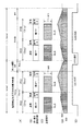
図5に示す例は、位置検出装置200のセンサ210から発光制御用期間PDに送信する信号を、周波数f0の交流信号からなるバースト状信号の繰り返し周期を、位置検出用信号SBとは異ならせるようにした発光制御信号LBaとした場合のタイミングチャートを示す図である。
In the example shown in FIG. 5, the signal transmitted from the
この図5の例においても、位置検出装置200では、図5(A)に示すように、例えば7.5ミリ秒の周期Tで、位置検出用期間PXYと発光制御用期間PDと休止期間PPとを繰り返す。したがって、この図5の例においては、位置検出用期間PXYにおける動作は、図5(B)〜(D)に示すように、図4の例の場合と同様である。 Also in the example of FIG. 5, in the position detection device 200, as shown in FIG. 5 (A), for example, with a period T of 7.5 milliseconds, the position detection period PXY, the light emission control period PD, and the rest period PP And repeat. Therefore, in the example of FIG. 5, the operation in the position detection period PXY is the same as that of the example of FIG. 4, as shown in FIGS. 5 (B) to 5 (D).
そして、この図5の例の発光制御用期間PDにおいては、切り替え接続回路223は、図5(B)に示すように、当該発光制御用期間PDの全体に亘って端子T側に接続されるのではなく、位置検出用期間PXYにおける送信期間と同じ1.5ミリ秒ずつの期間だけ端子T側に接続するようにし、かつ、当該端子T側に接続する期間の繰り返し周期を、位置検出用期間PXYの繰り返し周期(1.5ミリ秒)よりも短時間とする。
Then, in the light emission control period PD of the example of FIG. 5, the
すなわち、この例では、発光制御信号LBaを構成するバースト状信号の信号連続時間は、位置検出用信号SBx及びSByと同一であるが、発光制御信号LBaの繰り返し周期が、位置検出用信号SBxと位置検出用信号SByとの繰り返し周期よりも短時間とする。なお、発光制御用期間PDは3ミリ秒であるので、この例では、図5(B)、(C)に示すように、当該発光制御用期間PDの最後の発光制御信号LBaの信号連続時間は、図示のように1.5ミリ秒以下となる。 That is, in this example, the signal continuous time of the burst-shaped signal constituting the light emission control signal LBa is the same as the position detection signals SBx and SBy, but the repetition period of the light emission control signal LBa is the same as the position detection signal SBx. The time is shorter than the repetition period with the position detection signal SBy. Since the light emission control period PD is 3 milliseconds, in this example, as shown in FIGS. 5 (B) and 5 (C), the signal continuous time of the last light emission control signal LBa of the light emission control period PD. Is 1.5 milliseconds or less as shown in the figure.
ここで、発光制御用期間PDにおいて、切り替え接続回路223は、端子T側に接続されていないときには、端子R側に接続しておくようにしてもよいし、端子T及び端子Rのいずれにも接続しない状態にしていてもよい。なお、切り替え接続回路223を端子R側に接続しておく場合であっても、処理制御部233は、この発光制御用期間PDにおいては、受信時の動作は行わないようにする。
Here, in the light emission control period PD, the
位置検出装置200において、この図5の例のように、発光制御用期間PDにおいて切り替え接続回路223を切り替え制御するようにすれば、発光制御用期間PDにおいては、図5(D)に示すように、発光制御信号LBaとして、1.5ミリ秒の信号連続期間のバースト状信号が、位置検出用期間PXYの繰り返し周囲(1.5ミリ秒)よりも短時間で繰り返されるセンサ210から送出する状態となる。
If the position detection device 200 switches and controls the
以上のように、図5の例においては、バースト状信号の繰り返し周期を、位置検出用期間PXYのそれよりも短時間とすることで、電子ペン用カートリッジの電子回路の信号生成回路343においては、図5(D)及び図5(E)に示すように、発光制御用期間PDにおいて、閾値Ethを超えてLED342を発光点灯状態とすることができる発光駆動制御信号が生成される。
As described above, in the example of FIG. 5, by setting the repetition period of the burst-shaped signal to be shorter than that of the position detection period PXY, the
なお、この図5の例に場合には、発光制御用期間PDにおける端子T側の接続期間は、位置検出用期間におけるそれと同一の1.5ミリ秒としたが、同一である必要はない。また、発光制御用期間PDにおける発光制御信号LBaとしてのバースト状信号の振幅も、位置検出用期間の振幅M1と同一とする必要はない。要は、電子ペン1が、発光制御用期間PDにおいて、閾値Ethを超えてLED342を発光点灯状態とすることができる発光駆動制御信号を、発光制御信号LBaから生成することができればよい。
In the case of the example of FIG. 5, the connection period on the terminal T side in the light emission control period PD is 1.5 milliseconds, which is the same as that in the position detection period, but it does not have to be the same. Further, the amplitude of the burst signal as the light emission control signal LBa in the light emission control period PD does not have to be the same as the amplitude M1 of the position detection period. In short, it suffices if the
<<第3の例>>
上述の例では、位置検出装置200は、位置検出用信号と発光制御信号とを、それぞれ別々の位置検出用期間PXYと発光制御用期間PDとにおいて、センサ210から時分割信号で送出するように構成している。しかし、位置検出装置200のセンサ210から送出する位置検出用信号と発光制御信号とは別々の信号とはせずに、一つの信号により兼用するようにすることもできる。
<< Third example >>
In the above example, the position detection device 200 transmits the position detection signal and the light emission control signal from the
図6は、この第3の例の場合における、位置検出装置200及び電子ペン1の動作シーケンス例を説明するためのタイミングチャートを示すものである。この例においては、位置検出装置200の処理制御部233は、図6(A)に示すように、前述の例と同様に、例えば7.5ミリ秒の周期Tで、位置検出動作及び電子ペン1のLED342の発光制御処理動作を繰り返すように処理制御するが、前述の例と異なり、独立の発光制御用期間PDは存在しない。
FIG. 6 shows a timing chart for explaining an operation sequence example of the position detection device 200 and the
すなわち、図6(A)に示すように、この第3の例においては、位置検出装置200における位置検出及び発光制御のための処理の1周期を位置検出及び発光制御兼用期間PXYDと、休止期間PPとからなるものとする。そして、位置検出及び発光制御兼用期間PXYDは、前半のX座標位置検出及び発光制御兼用期間PXDと、後半のY座標位置検出及び発光制御兼用期間PYDとからなるものとする。 That is, as shown in FIG. 6A, in this third example, one cycle of the processing for position detection and light emission control in the position detection device 200 is divided into a position detection and light emission control combined period polypropylene and a rest period. It shall consist of PP. The position detection and light emission control combined period PXYD is composed of the first half X coordinate position detection and light emission control combined period PXD and the latter half Y coordinate position detection and light emission control combined period PYD.
例えば、前述の例と同様に1周期が7.5ミリ秒の場合、図6(A)に示すように、1周期Tを、6ミリ秒の位置検出及び発光制御兼用期間PXYDと、1.5ミリ秒の休止期間PPとからなるものとする。そして、位置検出及び発光制御兼用期間PXYDの前半の3ミリ秒は、X座標位置検出及び発光制御兼用期間PXDとし、後半の3ミリ秒は、Y座標位置検出及び発光制御兼用期間PYDとする。 For example, when one cycle is 7.5 milliseconds as in the above example, as shown in FIG. 6 (A), one cycle T is set to 6 milliseconds for position detection and light emission control combined period polypropylene, and 1. It shall consist of a rest period PP of 5 milliseconds. The first 3 milliseconds of the position detection and light emission control combined period PXYD is the X coordinate position detection and light emission control combined period PXD, and the latter 3 milliseconds is the Y coordinate position detection and light emission control combined period PYD.
そして、X座標位置検出及び発光制御兼用期間PXD及びY座標位置検出及び発光制御兼用期間PYDのそれぞれにおいては、処理制御部233により、切り替え接続回路223が、図6(B)に示すように、3ミリ秒の始点から2.25ミリ秒の期間は、送信側端子Tに切り替えられ、残りの0.75ミリ秒の期間は、受信側端子Rに切り替えられるように制御される。
Then, in each of the X-coordinate position detection and light emission control combined period PXD and the Y coordinate position detection and light emission control combined period PYD, the
そして、X座標位置検出及び発光制御兼用期間PXDにおいては、処理制御部233により、選択回路213が、切り替え接続回路223が送信側端子Tに切り替えられている期間及び受信側端子Rに切り替えられている期間のそれぞれにおいて、X軸方向ループコイル群211Xの各ループコイルを順次に選択するように制御される。また、Y座標位置検出及び発光制御兼用期間PYDにおいては、処理制御部233により、同様にして、選択回路213が、切り替え接続回路223が送信側端子Tに切り替えられている期間及び受信側端子Rに切り替えられている期間のそれぞれにおいて、Y軸方向ループコイル群212Yの各ループコイルを順次に選択するように制御される。
Then, in the X coordinate position detection and light emission control combined period PXD, the
なお、休止期間PPは、上述の例と同様に、位置検出装置では、送信動作及び受信動作のいずれをも休止する期間である。 The pause period PP is a period in which both the transmission operation and the reception operation are suspended in the position detection device, as in the above example.
位置検出装置200では、X座標位置検出及び発光制御兼用期間PXD及びY座標位置検出及び発光制御兼用期間PYDにおいて切り替え接続回路223が送信側端子Tに切り替えられている期間においては、図6(C)に示すように、発振器221からの周波数がf0であって、電流ドライバが処理制御部233により制御されることにより振幅M3とされている交流信号が、X座標位置検出及び発光制御兼用期間PXD及びY座標位置検出及び発光制御兼用期間PYDのうちの2.25ミリ秒に亘る信号連続時間において、位置検出及び発光制御用信号SLBとして、センサ210に供給される。このときセンサ210からは、電子ペン1に対しては、この位置検出及び発光制御用信号SLBは、図6(C)に示すように、バースト状信号となっている。
In the position detection device 200, FIG. 6 (C) is a period in which the
そして、前述の例と同様にして、位置検出装置200は、X座標位置検出及び発光制御兼用期間PXDのうちの切り替え接続回路223が端子Rに切り替えられる受信期間において、X軸方向ループコイル群211Xの各ループコイルに誘起される電圧を検出することで、電子ペン1の指示位置を検出すると共に、電子ペン1に印加されている筆圧の検出処理を行う。また、Y座標位置検出及び発光制御兼用期間PYDのうちの切り替え接続回路223が端子Rに切り替えられる受信期間においては、Y軸方向ループコイル群212Yの各ループコイルに誘起される電圧を検出することで、電子ペン1の指示位置を検出すると共に、電子ペン1に印加されている筆圧の検出処理を行う。
Then, in the same manner as in the above-mentioned example, the position detection device 200 has the X-axis direction
一方、電子ペン1の電子ペン用カートリッジの共振回路340Rは、位置検出装置200のセンサ210からの位置検出及び発光制御用信号SLBを受信して、センサ210に帰還する。また、電子ペン1の電子ペン用カートリッジの電子回路34においては、共振回路340Rで受信した位置検出及び発光制御用信号SLBが信号生成回路343の整流用ダイオード3432及び3433により整流され、その整流電流によりコンデンサ3434が充電されて、当該コンデンサ3434に、バースト信号SLBの電力が蓄積される(図6(D)参照)。
On the other hand, the
コンデンサ3434の両端間電圧としての発光駆動制御電圧EDは、図6(D)に示すように、位置検出及び発光制御用信号SLBが存在している間は、蓄積動作(充電動作)により上昇し、位置検出及び発光制御用信号SLBが無くなると、放電動作により低下する。
As shown in FIG. 6D, the light emission drive control voltage ED as the voltage between both ends of the
そして、この図6の例においては、コンデンサ3434の両端間電圧としての発光駆動制御電圧EDは、位置検出及び発光制御兼用期間PXYDのそれぞれの期間内において、図6Dに示すように、LED342を発光させる駆動電圧の閾値Ethを超えるようになる。したがって、この例においても、信号生成回路343においては、電子ペン1が位置検出装置200のセンサ210に近づくと、図6(E)に示すようにLED342を発光駆動するようにする発光駆動制御電圧EDを生成することができるものである。
Then, in the example of FIG. 6, the emission drive control voltage ED as the voltage between both ends of the
なお、この図6の例の位置検出及び発光制御用信号SLBは、一例であり、その振幅、信号連続時間または繰り返し周期のいずれか、あるいは、2つ以上を変えることで、LED342の点灯期間を制御することができる。また、図6の例の1周期T、位置検出及び発光制御兼用期間PXYD及び休止期間PPの長さは、一例であり、種々の値に設定することができる。
The position detection and light emission control signal SLB in the example of FIG. 6 is an example, and the lighting period of the
<電子ペン用カートリッジ3の電子回路の信号生成回路の他の例>
上述の実施形態の電子ペン用カートリッジの電子回路34の信号生成回路343は、半波2倍圧整流回路を用いるようにしたが、これに限られるものではなく、その他種々の整流回路を用いることができる。
<Other Examples of Signal Generation Circuits of Electronic Circuits for
The
図7は、上述の例の半波整流回路を2組、直列に接続して、両波倍電圧整流回路の構成とした信号生成回路343Aを備える電子回路34Aの例を示すものである。この図7において、前述の図3に示した電子回路34と同一部分には、同一参照符号を付してある。
FIG. 7 shows an example of an
この図7の例の電子回路34Aにおいて、共振回路340Rは、図3の例と同様に、コイル311と、コンデンサ341と、筆圧検出部材36で構成される可変容量コンデンサ36Cの並列回路で構成されているが、この例では、コイル311の一端側が接地されている。
In the
そして、この例では、この共振回路340Rで受信された、センサ210からの発光制御信号から、信号生成回路343Aにおいて、LED342を発光駆動する発光駆動制御電圧EDを生成する。
Then, in this example, the light emission control voltage ED that drives the
そして、この例では、信号生成回路343Aは、コンデンサ3431a及び3434aと、整流用のダイオード3432a及び3433aとからなり、図3の例の信号生成回路343と同様の構成の第1の半波2倍圧整流回路と、コンデンサ3431b及び3434bと、整流用のダイオード3432b及び3433bとからなり、図3の例の信号生成回路343と同様の構成の第2の半波2倍圧整流回路とが、直列に接続されて構成されている。この場合に、ダイオード3432aのアノードと、ダイオード3433bのカソードとが接続されて、その接続点が接地される。また、コンデンサ3434aとコンデンサ3434bとが直列に接続されると共に、このコンデンサ3434aとコンデンサ3434bとの接続点が接地される。そして、コンデンサ3434aとコンデンサ3434bとの直列回路に対して並列に、LED342が接続される。
Then, in this example, the
この図7の例においては、周波数f0の交流信号から発光制御信号を両波整流することでLED342の発光駆動制御電圧EDを生成するので、より効率良く、センサ210からの発光制御信号から発光駆動制御電圧EDを生成することができる。
In the example of FIG. 7, since the light emission control voltage ED of the
[第2の実施形態]
以上説明した第1の実施形態においては、位置検出装置200は、そのセンサ210から送出する発光制御信号を、電磁結合しているか否かに関わらず、同じものとした。しかし、電子ペン1と位置検出装置200のセンサ210との電磁結合状態に応じて、位置検出装置200は、センサ210から電子ペン1に送出する発光制御信号を変更制御するようにしてもよい。第2の実施形態は、位置検出装置200をそのように構成する場合の例である。
[Second Embodiment]
In the first embodiment described above, the position detection device 200 has the same light emission control signal transmitted from the
第2の実施形態における位置検出装置200及び電子ペン1のハードウエア構成は、上述した第1の実施形態と全く同様である。この第2の実施形態では、位置検出装置200の処理制御部233におけるソフトウェア処理が、第1の実施形態とは異なる。
The hardware configuration of the position detection device 200 and the
図8は、この第2の実施形態における処理制御部233におけるソフトウェア処理の流れの概要を示すフローチャートである。なお、以下の説明においては、位置検出装置200は、図4に示すように、周期Tの期間内に、時分割で、位置検出用信号SBx,SByと、発光制御信号LBとを、センサ210から送出する場合の例として説明する。
FIG. 8 is a flowchart showing an outline of the flow of software processing in the
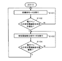
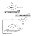
すなわち、この第2の実施形態においては、処理制御部233は、先ず、センサ210が電子ペン1と電磁結合状態になる前の待機時モードを実行する(ステップS101)。
That is, in this second embodiment, the
この待機時モードにおいては、この例においては、全ての周期Tの期間で位置検出用信号SBx,SBy及び発光制御信号LBを送出するのではなく、周期Tの複数倍、例えば周期Tの100倍の期間(100T=750ミリ秒)ごとに、位置検出用信号SBx,SBy及び発光制御信号LBを送出する信号送出期間と、送出しない休止期間とを繰り返すようにする(図9(A)参照)。 In this standby mode, in this example, the position detection signals SBx, SBy and the light emission control signal LB are not transmitted in all the periods of the period T, but are multiple times the period T, for example, 100 times the period T. The signal transmission period for transmitting the position detection signals SBx, SBy and the light emission control signal LB and the non-transmission pause period are repeated every period (100T = 750 milliseconds) (see FIG. 9 (A)). ..
したがって、この待機時モードの状態にある位置検出装置200のセンサ210に電子ペン1が近づくと、すなわち、待機時モードの電子ペン接近状態になると、電子ペン1の電子ペン用カートリッジ3においては、信号送出期間ではLED342が点灯状態となり、休止期間ではLED342が消灯状態となるので、人間の目には、LED342は点滅する状態となって見える(図9(B)参照)。
Therefore, when the
なお、上述の「待機時モードの電子ペン接近状態」とは、電子ペン1Bとセンサ210とは電磁結合している状態となっているが、電子ペン1Bからの帰還信号のレベルが小さいため、センサ210で、電子ペン1Bにより指示された位置を正確に検出することができない状態を言う。
The above-mentioned "standby mode electronic pen approaching state" is a state in which the
位置検出装置200の処理制御部233は、この待機時モードでは、電子ペン1が、上記の電子ペン接近状態よりもさらにセンサ210に近づいて、電子ペン1とセンサ210とが、位置検出として有効に電磁結合する状態(以下、有効電磁結合状態という)となったか否かを、前述したように、センサ210のループコイルに誘起される電圧を監視することで判別する(ステップS102)。なお、この第2の実施形態においては、この有効電磁結合状態とは、電子ペン1Bのセンサ上の位置を正確に検出することができる状態を言う。
In this standby mode, the
そして、このステップS102で、電子ペン1とセンサ210とが有効電磁結合状態となってはいないと判別したときには、処理制御部233は、処理をステップS101に戻して、ステップS101及びステップS102を繰り返す。
Then, when it is determined in step S102 that the
また、ステップS102で、電子ペン1とセンサ210とが有効電磁結合状態となったと判別したときには、処理制御部233は、待機時モードから有効電磁結合時モードに変更し、全ての周期Tの期間で位置検出用信号SBx,SBy及び発光制御信号LBを送出する(ステップS103;図9(C)参照)。
Further, when it is determined in step S102 that the
この電磁結合時モードにおいては、全ての周期Tの期間で発光制御信号が送出されるので、前述したように、電子ペン1の電子ペン用カートリッジ3のLED342は、点灯する状態となって見える(図9(D)参照)。
In this electromagnetic coupling mode, since the light emission control signal is transmitted during the entire period T, the
位置検出装置200の処理制御部233は、この有効電磁結合時モードでは、電子ペン1がセンサ210から遠ざかって、電子ペン1とセンサ210との有効電磁結合状態が解除される状態になったか否か判別する(ステップS104)。
In this effective electromagnetic coupling mode, the
そして、このステップS104で、電子ペン1とセンサ210との有効電磁結合状態が解除される状態になってはいないと判別したときには、処理制御部233は、処理をステップS103に戻して、ステップS103及びステップS104を繰り返す。
Then, when it is determined in step S104 that the effective electromagnetic coupling state between the
また、ステップS104で、電子ペン1とセンサ210との有効電磁結合状態が解除される状態となったと判別したときには、処理制御部233は、処理をステップS101に戻して、有効電磁結合時モードから待機時モードに変更し、このステップS101以降の処理を繰り返す。
Further, when it is determined in step S104 that the effective electromagnetic coupling state between the
以上説明したように、この第2の実施形態においては、電子ペン1の電子ペン用カートリッジ3においては、位置検出装置200のセンサ210からの信号を受信することにより、センサ210と有効電磁結合する前の状態のときには、LED342が点滅し、センサ210と有効電磁結合した状態になると、LED342が点灯状態となる。
As described above, in the second embodiment, the
したがって、電子ペン1の使用者は、LED342の点滅状態あるいは点灯状態の発光態様から、センサ210との電磁結合状態を容易に把握することができて便利である。
Therefore, the user of the
なお、上述の例では、休止期間には、位置検出用信号SBの送出も休止するようにしたが、発光制御信号LBのみを休止するようにしてもよい。 In the above example, the transmission of the position detection signal SB is also suspended during the pause period, but only the light emission control signal LB may be suspended.
また、上述の第2の実施形態の例は、図4に示した、周期Tの期間内に、時分割で、位置検出用信号SBx,SByと発光制御信号LBとを、センサ210から送出する場合の例としたが、図5に示した位置検出用信号SBx,SByと、発光制御信号LBaとを時分割で送出するようにした、発光制御用期間PDにおける発光制御信号の他の例の第1の例の場合にも適用することができる。また、第2の実施形態は、発光制御用期間PDにおける発光制御信号の他の例の第2の例及び第3の例の場合にも適用することができるものである。
Further, in the example of the second embodiment described above, the position detection signals SBx and SBy and the light emission control signal LB are transmitted from the
[第2の実施形態の変形例]
上述の第2の実施形態の例においては、処理制御部233においては、待機時モードにおいては、信号送出期間と休止期間とを設けることで、電子ペン1ではLED342を点滅させるようにし、有効電磁結合時モードにおいては、休止期間を設けないようにすることで、LED342が点灯させるようにすることで、両モードを使用者が把握できるようにした。すなわち、LED342の点滅と点灯という発光態様の違いにより、両モードを使用者が把握できるようにした。しかし、待機時モードと有効電磁結合時モードとを使用者に把握させるようにする、LED342の発光態様の違いとしては、点滅と点灯に限られるものではない。
[Modified example of the second embodiment]
In the example of the second embodiment described above, in the
例えば、待機時モードにおいても、有効電磁結合時モードと同様に、全ての周期Tの期間で位置検出用信号SBx,SByと発光制御信号LBとを送出するが、待機時モードにおける位置検出用信号SBx,SBy及び発光制御信号LBの振幅MAと、有効電磁結合時モードにおける位置検出用信号SBx,SBy及び発光制御信号LBの振幅MBとを異ならせ、振幅MA<振幅MBとするようにする。 For example, in the standby mode as well, as in the effective electromagnetic coupling mode, the position detection signals SBx and SBy and the light emission control signal LB are transmitted during the entire period T, but the position detection signal in the standby mode is transmitted. The amplitude MA of the SBx, SBy and the light emission control signal LB is different from the amplitude MB of the position detection signals SBx, SBy and the light emission control signal LB in the effective electromagnetic coupling mode so that the amplitude MA <amplitude MB.
このようにすれば、待機時モードにおける電子ペン1のLED342の発光強度と、有効電磁結合時モードにおける電子ペン1のLED342の発光強度の違いから、両モードを使用者が把握することができる。そして、振幅MA<振幅MBとされるので、有効電磁結合時モードにおける電子ペン1のLED342の発光強度が、待機時モードのそれよりも大きいので、電子ペン1の使用時に、センサ210上において明るく発光することになり、電子ペン1のペン先側が明るくなって使い勝手が良くなるという効果がある。
In this way, the user can grasp both modes from the difference between the light emitting intensity of the
なお、この変形例の場合において、待機時モードと有効電磁結合時モードとで、振幅を変更制御する信号は、発光制御信号LBのみとしてもよい。 In the case of this modification, the light emission control signal LB may be the only signal for changing and controlling the amplitude between the standby mode and the effective electromagnetic coupling mode.
また、この第2の実施形態の変形例も、発光制御用期間PDにおける発光制御信号の他の例の第1の例〜第3の例のいずれの例の場合にも適用することができるものである。 Further, the modified example of this second embodiment can also be applied to any of the first to third examples of other examples of the light emission control signal in the light emission control period PD. Is.
[第3の実施形態]
以上の第1の実施形態及び第2の実施形態においては、電子ペンの発光素子としては、1個の発光素子であって、白色を含む特定の単色のLEDで構成した場合を想定した。しかし、電子ペンに設ける発光素子としては、複数個であってもよい。この第3の実施形態においては、電子ペンに、種々の発光色を呈するように、発光色が例えば赤、青、緑の3原色のそれぞれである3個のLEDを設け、当該3個のLEDによる発光色(合成による発光色を含む)を位置検出装置からの発光制御信号により、変更制御するようにする。
[Third Embodiment]
In the above-mentioned first embodiment and the second embodiment, it is assumed that the light emitting element of the electronic pen is one light emitting element and is composed of a specific single color LED including white. However, the number of light emitting elements provided in the electronic pen may be plural. In the third embodiment, the electronic pen is provided with three LEDs whose emission colors are, for example, three primary colors of red, blue, and green so as to exhibit various emission colors, and the three LEDs are provided. The emission color (including the emission color by synthesis) is changed and controlled by the emission control signal from the position detection device.
図10(A)及び(B)は、この第3の実施形態の場合における電子ペン1Bの電子ペン用カートリッジ3Bの構成例を示す図であり、図2に示した第1の実施形態の電子ペン1の電子ペン用カートリッジ3と同一部分には、同一の参照符号を付してある。
10 (A) and 10 (B) are diagrams showing a configuration example of the electronic pen cartridge 3B of the
この第3の実施形態における電子ペン1Bの電子ペン用カートリッジ3Bは、図10(B)に示すように、筒状体32の第1の筒状体部321内のプリント基板33上に、発光色が、赤、青、緑の3原色のそれぞれである3個のLED342r,LED342g,LED342bが設けられる。そして、筒状体32の第1の筒状体部321の外周部には、図10(A)に示すように、3個のLED342r,LED342g,LED342bに対応して、それらの発光光を外部に放射することができるようにするための窓部321Wrgbが形成されている。
As shown in FIG. 10B, the electronic pen cartridge 3B of the
そして、このこの第3の実施形態における電子ペン1Bの電子ペン用カートリッジ3Bにおいては、電子回路34Bが図11に示すように構成される。その他は、図2に示した第1の実施形態の電子ペン1の電子ペン用カートリッジ3と同様である。
Then, in the electronic pen cartridge 3B of the
次に、図11に示す電子回路34Bについて説明する。この例の電子回路34Bは、信号生成回路343のコンデンサ3434に蓄積される電圧EDが供給されるLEDが、3個のLED342r,342g,342bとされる点が異なるだけで、その他の構成は、図2に示した第1の実施形態の電子ペン1の電子ペン用カートリッジ3が備える電子回路34と同様である。
Next, the
すなわち、この第3の実施形態における電子回路34Bにおいては、コンデンサ3434に並列に、抵抗344rとLED342rとの直列回路と、抵抗344gとLED342gとの直列回路と、抵抗344bとLED342bとの直列回路とのそれぞれが接続されている。
That is, in the
この電子回路34Bにおいては、発光色が赤であるLED342rが発光駆動される閾値電圧をEthr、発光色が緑であるLED342gが発光駆動される閾値電圧をEthg、発光色が青であるLED342bが発光駆動される閾値電圧をEthb、とすると、Ethr<Ethg<Ethbとなるように、抵抗344r、抵抗344g、抵抗344bのそれぞれの抵抗値が選定されて構成されている。
In this
したがって、コンデンサ3434の蓄積電圧である発光駆動制御電圧EDが、Ethr≦ED<Ethgのときには、発光色が赤色のLED342rのみが発光する。そして、コンデンサ3434の蓄積電圧EDが、Ethg≦ED<Ethbのときには、発光色が赤色のLED342rと、緑のLED342gとが発光して、合成色として黄色の発光色となる。さらに、コンデンサ3434の蓄積電圧EDが、Ethb≦EDのときには、発光色が赤色のLED342rと、緑のLED342gと、青のLED342bとの全てが発光して、合成色として白色の発光色となる。
Therefore, when the emission drive control voltage ED, which is the accumulated voltage of the
一方、この第3の実施形態においては、位置検出装置200においては、処理制御部233によるソフトウェア処理により、位置検出装置200のセンサ210と電子ペン1Bとの電磁結合状態及び電子ペン1Bのセンサ210との接触状態に応じた発光制御信号が供給されるように構成されている。
On the other hand, in the third embodiment, in the position detection device 200, the electromagnetic coupling state between the
すなわち、この第3の実施形態における位置検出装置200の処理制御部233は、上述した第2の実施形態と同様に、待機時モードと、電磁結合時モードとを備える。さらに、この第3の実施形態における位置検出装置200の処理制御部233は、電子ペン1Bからの帰還信号から検出される電子ペン1Bに印加されている筆圧値を検出することで、電子ペン1Bがセンサ210上に接触しているかどうかを検出し、接触しているときには、電子ペンの接触時モードとなるように構成されている。ここで、処理制御部233は、電子ペン1Bがセンサ210上に接触しているかどうかは、電子ペン1Bにおける筆圧値が0以上の所定値以上となっているかどうかにより判断する。
That is, the
そして、以下に説明するように、この第3の実施形態の位置検出装置200では、図4に示した第1の実施形態の場合と同様に、周期Tの期間を位置検出用期間PXYと、発光制御用期間PDと、休止期間とに分け、時分割で、位置検出用信号SBx,SByと、発光制御信号とを、センサ210から送出するようにする。ただし、この第3の実施形態の位置検出装置200においては、発光制御用期間PDに送出する発光制御信号を、上述した、待機時モードと、電磁結合時モードと、接触時モードとに応じて変更制御する。これにより、電子ペン1Bの電子ペン用カートリッジ3Bの発光素子としての3個のLED342r,LED342g,LED342bによる合成の発光色を、上述の待機時モードと、電磁結合時モードと、接触時モードとに応じて変更制御するようにする。
Then, as described below, in the position detection device 200 of the third embodiment, the period of the cycle T is set to the position detection period PXY, as in the case of the first embodiment shown in FIG. The light emission control period PD and the pause period are divided, and the position detection signals SBx and SBy and the light emission control signal are transmitted from the
図12は、この第3の実施形態における位置検出装置200の処理制御部233によるソフトウェア処理の流れを説明するためのフローチャートである。また、図13は、当該処理制御部233におけるソフトウェア処理の流れに応じたセンサ210からの送信信号と、電子ペン1Bの電子回路34Bの信号生成回路343の動作を説明するためのタイミングチャートである。以下に、図12及び図13を参照しながら、この第3の実施形態における位置検出装置200による電子ペン1Bの3個のLED342r,LED342g,LED342bの発光制御について説明する。
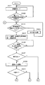
FIG. 12 is a flowchart for explaining the flow of software processing by the
なお、以下に説明する例においては、処理制御部233が、電流ドライバのゲインを制御することで、発光制御用期間PDに送出する発光制御信号の振幅を制御し、これにより、電子ペン1Bの3個のLED342r,LED342g,LED342bの発光制御をするようにする。
In the example described below, the
すなわち、この第3の実施形態においては、処理制御部233は、先ず、センサ210が電子ペン1と電磁結合状態になる前の待機時モードを実行する(ステップS201)。
That is, in this third embodiment, the
この待機時モードにおいては、この例においては、図13(A)に示すように、全ての周期Tの期間で位置検出用信号SBx,SBy及びバースト状信号からなる発光制御信号LB1を送出するが、発光制御信号LB1の振幅Mrを、この例では、位置検出用信号SBx,SByの振幅M1と等しくする。 In this standby mode, in this example, as shown in FIG. 13A, the light emission control signal LB1 composed of the position detection signals SBx, SBy and the burst signal is transmitted during the entire period T. In this example, the amplitude Mr of the light emission control signal LB1 is made equal to the amplitude M1 of the position detection signals SBx and SBy.
この待機時モードの状態にある位置検出装置200のセンサ210に電子ペン1Bが近づくと、電子ペン用カートリッジ3Bの電子回路34Bの信号生成回路343のコンデンサ3434に得られる発光駆動制御電圧EDは、図13(B)に示すように、周期T毎に赤のLED342rを発光駆動する閾値電圧Ethrを超えるが、緑の閾値電圧Ethg及び及び青の閾値電圧Ethbは超えない状態となる。このため、この待機時モードの電子ペン接近状態になると、電子ペン用カートリッジ3Bの赤のLED342rのみが点灯する状態となり(図13(C)参照)、待機時モードの電子ペン接近状態であることを使用者に報知することができる。この場合に、前述もしたように、コンデンサ3434に得られる発光駆動制御電圧EDは、周期T毎に、赤のLED342rを発光駆動する閾値電圧Ethrを超えるので、周期Tが例えば7.5ミリ秒と短いことと相俟って、赤のLED342rは、人間の目には、赤で点灯しているように見える。
When the
次に、位置検出装置200の処理制御部233は、この待機時モードでは、電子ペン1Bが、上記の電子ペン接近状態よりもさらにセンサ210に近づいて、電子ペン1Bとセンサ210とが、位置検出として有効に電磁結合する状態(以下、有効電磁結合状態という)となったか否かを、前述したように、センサ210のループコイルに誘起される電圧を監視することで判別する(ステップS202)。なお、この第3の実施形態においては、この有効電磁結合状態とは、電子ペン1Bのセンサ上の位置を正確に検出することができる状態ではあるが、電子ペン1Bがセンサ210に接触していない、いわゆるホバーリング状態となっている状態を言う。
Next, in the
そして、このステップS202で、電子ペン1Bとセンサ210とが有効電磁結合状態となってはいないと判別したときには、処理制御部233は、処理をステップS201に戻して、ステップS201及びステップS202を繰り返す。
Then, when it is determined in step S202 that the
また、ステップS202で、電子ペン1Bとセンサ210とが有効電磁結合状態となったと判別したときには、処理制御部233は、待機時モードから有効電磁結合時モードに変更し、周期Tの期間の内の発光制御用期間において、発光制御信号LB1の振幅Mrより大きい振幅Mg(Mg>Mr)の発光制御信号LB2を送出する(ステップS203;図13(D)参照)。
Further, when it is determined in step S202 that the
この有効電磁結合時モードにおいては、電子ペン用カートリッジ3Bの電子回路34Bの信号生成回路343のコンデンサ3434に得られる発光駆動制御電圧EDは、図13(E)に示すように、周期T毎に赤のLED342rを発光駆動する閾値電圧Ethr及び緑のLED342gを発光駆動する閾値電圧Ethgを超えるが、青の閾値電圧Ethbは超えない状態となる。
In this effective electromagnetic coupling mode, the emission drive control voltage ED obtained in the
このため、有効電磁結合時モードにおいては、電子ペン用カートリッジ3Bの赤のLED342r及び緑のLED342gが点灯する状態となり(図13(F)及び(G)参照)、電子ペン1Bは、合成の黄色の発光する状態となって、有効電磁結合時モードであることを使用者に報知することができる。
Therefore, in the effective electromagnetic coupling mode, the
位置検出装置200の処理制御部233は、この有効電磁結合時モードでは、電子ペン1Bがセンサ210から遠ざかって、電子ペン1Bとセンサ210との有効電磁結合状態が解除される状態になったか否か判別する(ステップS204)。
In this effective electromagnetic coupling mode, the
そして、このステップS204で、電子ペン1Bとセンサ210との有効電磁結合状態が解除される状態になっていると判別したときには、処理制御部233は、処理をステップS201に戻して、上述したステップS201以降の処理を繰り返す。
Then, when it is determined in step S204 that the effective electromagnetic coupling state between the
また、ステップS204で、電子ペン1Bとセンサ210との有効電磁結合状態が解除される状態とはなっていないと判別したときには、処理制御部233は、電子ペン1Bから受信した帰還信号から電子ペン1Bに印加されている筆圧値を検出して、その筆圧値が所定値以上となっているかどうかをチェックすることにより、電子ペン1Bがセンサ210に接触しているか否か判別する(ステップS205)。
Further, when it is determined in step S204 that the effective electromagnetic coupling state between the
このステップS205で、電子ペン1Bがセンサ210に接触してはいないと判別したときには、処理制御部233は、処理をステップS203に戻して、このステップS203以降の処理を繰り返す。
When it is determined in step S205 that the
また、ステップS205で、電子ペン1Bがセンサ210に接触していると判別したときには、処理制御部233は、有効電磁結合時モードから電子ペンの接触時モードに変更し、周期Tの期間の内の発光制御用期間において、発光制御信号LB2を構成するバースト状信号の振幅Mgより大きい振幅Mb(Mb>Mg)のバースト状信号である発光制御信号LB3を送出する(ステップS206;図13(H)参照)。
Further, when it is determined in step S205 that the
この電子ペンの接触時モードにおいては、電子ペン用カートリッジ3Bの電子回路34Bの信号生成回路343のコンデンサ3434に得られる発光駆動制御電圧EDは、図13(I)に示すように、周期T毎に赤のLED342rを発光駆動する閾値電圧Ethr、緑の閾値電圧Ethg及び青の閾値電圧Ethbの全てを超える状態となる。
In the contact mode of the electronic pen, the emission drive control voltage ED obtained in the
このため、この電子ペンの接触時モードにおいては、電子ペン用カートリッジ3Bの赤のLED342r、緑のLED342g及び青のLED342bのすべてが点灯する状態となり(図13(J)、(K)及び(L)参照)、電子ペン1Bは、合成色である白色で発光する状態となって、電子ペンの接触時モードであることを使用者に報知することができる。
Therefore, the contact time mode of the electronic pen, the pen cartridge 3B red LED342r, a state where all the lights of the
以上のようにして、この第3の実施形態においては、位置検出装置200からの発光制御信号により、電子ペン1Bに設けた発光素子による発光色を、制御することができる。そして、上述の例においては、位置検出装置200からは、位置検出装置200のセンサ210と電子ペン1Bとの電磁結合状態及び電子ペン1Bのセンサ210との接触状態に応じた発光制御信号が供給されて、電子ペン1Bでは、その発光素子の発光色により、電子ペン1Bと位置検出装置200との電磁結合関係や接触状態が使用者に報知される。したがって、使用者は、電子ペン1Bの発光素子の発光色を見るだけで、センサ210に対して電子ペン1Bがどのような結合関係状態にあるかを知ることができて、非常に便利である。
As described above, in the third embodiment, the emission color by the emission element provided in the
なお、上述の第3の実施形態では、処理制御部233は、発光制御信号を構成するバースト信号の振幅を、3つのモードに応じて変更することで、電子ペン1Bの発光素子の発光色を制御するようにしたが、図5に示した例のように、発光制御信号を構成するバースト信号の信号連続時間及び繰り返し周期を制御することで、電子ペン1Bの発光素子の発光色を制御するようにしてもよい。また、発光制御信号を構成するバースト信号の信号連続時間のみや、繰り返し周期のみを制御するようにしてもよいし、信号連続時間と、繰り返し周期と、振幅との2つ以上を組み合わせて制御するようにしてもよい。
In the third embodiment described above, the
また、この第3の実施形態においても、図6に示したように、位置検出用信号と発光制御信号とを共通の信号で兼用するようにして、当該共通の信号を構成するバースト信号の振幅、信号連続時間、繰り返し周期のいずれか、あるいは、それらの2つ以上を組み合わせて制御することで、電子ペン1Bの発光素子の発光色を制御するようにしてもよい。
Further, also in this third embodiment, as shown in FIG. 6, the position detection signal and the light emission control signal are shared by a common signal, and the amplitude of the burst signal constituting the common signal is used. , The signal continuous time, the repetition period, or a combination of two or more of them may be controlled to control the emission color of the light emitting element of the
[第4の実施形態]
第4の実施形態は、上述した第3の実施形態の変形例である。上述の第3の実施形態における電子ペン1Bにおいては、3個のLED342r,342g,342bの内の発光させるLEDの数を制御することで、発光色を変えるようにした。これに対して、第4の実施形態においては、当該第4の実施形態における電子ペン1Cの電子ペン用カートリッジ3Cに設ける3個のLED342r,342g,342bのそれぞれを切り替え制御することができるように構成し、発光色を、赤、緑、青とすることができるようにする。
[Fourth Embodiment]
The fourth embodiment is a modification of the third embodiment described above. In the
この第4の実施形態では、位置検出装置200の構成は、上述の第3の実施形態と全く同様とすることができる。そして、この第4の実施形態における電子ペン1Cの電子ペン用カートリッジ3Cは、機械構造的なハードウエア構成は、図10に示した第3の実施形態と同様であるが、電子回路の構成が異なる。
In this fourth embodiment, the configuration of the position detecting device 200 can be exactly the same as that of the third embodiment described above. The
図14は、この第4の実施形態における電子ペン1Cの電子ペン用カートリッジ3Cの電子回路34Cの回路構成例を示すものである。この図14において、前述の図11に示した第3の実施形態の電子ペン用カートリッジ3Bの電子回路34Bと同一部分には、同一参照符号を付してある。
FIG. 14 shows a circuit configuration example of the
すなわち、この第4の実施形態における電子回路34Cにおいては、コンデンサ3434に並列に、抵抗344rとLED342rとスイッチ回路345rの直列回路と、抵抗344gとLED342gとスイッチ回路345gと抵抗346gの直列回路と、抵抗344bとLED342bと抵抗346bの直列回路とのそれぞれが接続されている。
That is, in the
スイッチ回路345r及びスイッチ回路345gは、通常オン状態(閉状態)とされるスイッチ回路である。電子回路34Cにおいては、スイッチ回路345gは、LED342bが発光状態となって抵抗346bに電流が流れることにより当該抵抗346bの両端間に得られる電圧によりオフに制御される。
The switch circuit 345r and the switch circuit 345g are switch circuits that are normally turned on (closed). In the
また、スイッチ回路345rは、LED342gが発光状態となって抵抗346gに電流が流れることにより当該抵抗346gの両端間に得られる電圧によりオフに制御される。さらに、スイッチ回路345rは、LED342bが発光状態となって抵抗346bに電流が流れることにより当該抵抗346bの両端間に得られる電圧によってもオフに制御される。抵抗346gの両端間に得られる電圧と、抵抗346bの両端間に得られる電圧とによってスイッチ回路345rが制御されるように、図14の例では、オア回路347を介して、抵抗346gの両端間に得られる電圧と、抵抗346bの両端間に得られる電圧とがスイッチ回路345rの制御端子に供給されるように構成されている。
Further, the switch circuit 345r is controlled off by the voltage obtained between both ends of the resistor 346g when the
この第4の実施形態においても、位置検出装置200のセンサ210からは、図13に示したように、待機時モード、有効電磁結合時モード、電子ペンの接触時モードのそれぞれに応じた発光制御信号LB1,LB2,LB3が送出される。
Also in this fourth embodiment, as shown in FIG. 13, the
そのため、第4の実施形態において、待機時モードの状態にある位置検出装置200のセンサ210に電子ペン1Cが近づくと、電子ペン用カートリッジ3Cの電子回路34Cの信号生成回路343のコンデンサ3434に得られる発光駆動制御電圧EDは、図13(B)に示したように、周期T毎に赤のLED342rを発光駆動する閾値電圧Ethrのみを超える。このため、電子ペン用カートリッジ3Cの赤のLED342rのみが点灯する状態となり、待機時モードであることを使用者に報知することができる。
Therefore, in the fourth embodiment, when the
また、有効電磁結合時モードにおいては、電子ペン用カートリッジ3Cの電子回路34Cの信号生成回路343のコンデンサ3434に得られる発光駆動制御電圧EDは、図13(E)に示したように、周期T毎に赤のLED342rを発光駆動する閾値電圧Ethr及び緑のLED342gを発光駆動する閾値電圧Ethgを超える。
Further, in the effective electromagnetic coupling mode, the emission drive control voltage ED obtained in the
このため、有効電磁結合時モードにおいては、電子ペン用カートリッジ3Bの赤のLED342r及び緑のLED342gが点灯することが可能な状態となる。しかし、このとき、緑のLED342gが点灯することにより、当該緑のLED342gを通じて流れる電流により、抵抗346gの両端間に電圧が発生し、これにより、スイッチ回路345rがオフに制御される。したがって、赤のLED342rには駆動電流は流れず、赤のLED342rは点灯できず、消灯状態となる。したがって、有効電磁結合時モードにおいては、緑のLED342gのみが点灯する状態に切り替えられる。
Therefore, in the effective electromagnetic coupling mode, the
そして、電子ペンの接触時モードになると、電子ペン用カートリッジ3Cの電子回路34Cの信号生成回路343のコンデンサ3434に得られる発光駆動制御電圧EDは、図13(I)に示したように、周期T毎に赤のLED342rを発光駆動する閾値電圧Ethr、緑の閾値電圧Ethg及び青の閾値電圧Ethbの全てを超える状態となる。
Then, in the contact mode of the electronic pen, the emission drive control voltage ED obtained in the
このため、電子ペンの接触時モードにおいては、電子ペン用カートリッジ3Bの赤のLED342r、緑のLED342g及び青のLED342bのすべてが点灯することが可能な状態となる。しかし、このとき、青のLED342bが点灯することにより、当該青のLED342bを通じて流れる電流により、抵抗346bの両端間に電圧が発生し、これにより、スイッチ回路345r及びスイッチ回路345gがオフに制御される。したがって、赤のLED342r及び緑のLED342gには駆動電流は流れず、赤のLED342r及び緑のLED342gは点灯できず、消灯状態となる。したがって、電子ペンの接触時モードにおいては、青のLED342bのみが点灯する状態に切り替えられる。
Therefore, in the contact mode of the electronic pen, all of the
以上のようにして、この第4の実施形態においては、位置検出装置200からの発光制御信号により、電子ペン1Cに設けた発光素子としての赤、緑、青の3色のLED342r、LED342g及びLED342bを、位置検出装置200からの発光制御信号により切り替えて発光させるように制御することができる。
As described above, in the fourth embodiment, the red, green, and
そして、上述の例においては、電子ペン1Cでは、その発光素子の発光色の違いにより、電子ペン1Bと位置検出装置200との電磁結合関係や接触状態を使用者に報知することができるので、使用者は、電子ペン1Cの発光素子の発光色を見るだけで、センサ210に対して電子ペン1Bがどのような関係状態にあるかを知ることができて、非常に便利である。
Then, in the above-mentioned example, in the
なお、この第4の実施形態においても、上述の第3の実施形態と同様に、処理制御部233は、発光制御信号を構成するバースト信号の振幅を、3つのモードに応じて変更制御するだけでなく、発光制御信号を構成するバースト信号の信号連続時間や、繰り返し周期のみを制御するようにしてもよいし、信号連続時間と、繰り返し周期と、振幅との2つ以上を組み合わせて制御するようにしてもよい。
In this fourth embodiment as well, as in the third embodiment described above, the
また、この第4の実施形態も、上述の第3の実施形態と同様に、図6に示した位置検出用信号と発光制御信号とを共通の信号で兼用し、その共通の信号を構成するバースト信号の振幅、信号連続時間、繰り返し周期のいずれか、あるいは、それらの2つ以上を組み合わせて制御することで、電子ペン1Bの発光素子の発光色を制御することもできる。
Further, also in this fourth embodiment, similarly to the third embodiment described above, the position detection signal and the light emission control signal shown in FIG. 6 are shared by a common signal to form the common signal. The emission color of the light emitting element of the
なお、第3の実施形態及び第4の実施形態では、電子ペン1B,1Cと位置検出装置200のセンサ210との電磁結合状態や接触状態などの両者の位置的な結合状態に応じて位置検出装置200からの発光制御信号を変更制御することで、電子ペン1B,1Cの発光素子の発光色を変更制御するようにした。
In the third embodiment and the fourth embodiment, the position is detected according to the positional coupling state of the
しかし、第3の実施形態及び第4の実施形態の構成において、位置検出装置200からの発光制御信号による電子ペン1Bまたは電子ペン1Cの発光素子の発光色を変更制御態様は、電子ペン1Bまたは電子ペン1Cと位置検出装置200のセンサ210との位置的な結合関係に応じて、電子ペン1Bまたは電子ペン1Cの発光素子の発光色を変更制御する場合に限られるものではない。
However, in the configurations of the third embodiment and the fourth embodiment, the emission color of the light emitting element of the
例えば、位置検出装置200の処理制御部233が、パーソナルコンピュータなどの情報処理装置に接続されていて、当該情報処理装置の表示画面において、電子ペンによる描画色を使用者が設定することができるようにされている場合に、その使用者により設定された描画色の情報を処理制御部233が情報処理装置から取得し、当該設定された描画色に応じた発光制御信号を、位置検出装置200のセンサ210から送出するように構成することもできる。
For example, the
例えば、上述の例の電子ペン1Bまたは電子ペン1Cのように、発光素子の発光色が3種の場合には、その3種の色に対応する描画色の選択画面が、位置検出装置200の処理制御部233に接続された情報処理装置の表示画面に表示される。そして、その3種の描画色のいずれかが使用者により選択されたときには、その選択情報が処理制御部233に、情報処理装置から伝達される。処理制御部233は、情報処理装置から取得した選択された描画色を認識して、その描画色に応じた発光色で電子ペン1Bまたは電子ペン1Cを発光させるようにする発光制御信号を、センサ210から送出するようする。
For example, when the light emitting element has three kinds of emission colors like the
このように構成すれば、使用者は、位置検出装置200が接続されている情報処理装置を通じて選択した電子ペンによる描画色を、電子ペンの発光素子の発光色で確認することができるようになる。この場合に、電子ペンでは、信号生成回路で、発光制御信号から発光駆動制御信号を生成するだけの簡単な構成でよいので、位置検出装置200からの発光色の指定情報を受信してそれを解析し、発光素子の発光を制御するような複雑な構成は不要となるという顕著な効果を奏する。 With this configuration, the user can confirm the drawing color by the electronic pen selected through the information processing device to which the position detection device 200 is connected by the emission color of the light emitting element of the electronic pen. .. In this case, since the electronic pen may have a simple configuration in which the signal generation circuit only generates a light emission drive control signal from the light emission control signal, it receives the light emission color designation information from the position detection device 200 and uses it. It has a remarkable effect that a complicated configuration for controlling the light emission of the light emitting element by analysis is not required.
[第5の実施形態]
上述した実施形態の位置指示器の例の電子ペンでは、電子ペン用カートリッジを筐体内に1本のみを収納するようにした場合であった。この第5の実施形態では、筐体内に複数本の電子ペン用カートリッジを収納させ、ノック機構により、その複数本の電子ペン用カートリッジの内の1本を選択して、その選択した電子ペン用カートリッジのペン先部の先端を、筐体のペン先側の開口から突出させて使用するようにする。
[Fifth Embodiment]
In the electronic pen of the example of the position indicator of the above-described embodiment, only one electronic pen cartridge is stored in the housing. In the fifth embodiment, a plurality of electronic pen cartridges are stored in the housing, and one of the plurality of electronic pen cartridges is selected by the knock mechanism for the selected electronic pen. The tip of the pen tip of the cartridge should be projected from the opening on the pen tip side of the housing for use.
前述したように、第1の実施形態の電子ペン1の電子ペン用カートリッジ3は、ボールペンの替え芯6と互換性を取れる構成を備えるようにされている。市販のボールペンとしては、インク色の異なる替え芯を装着した多色ボールペンが存在する。この第5の実施形態は、電子ペン用カートリッジ3と同様の構成の電子ペン用カートリッジを、この多色ボールペンの筐体と同様の構成の筐体に収納することで構成される電子ペンを提供するものである。
As described above, the
図15(A)は、この第5の実施形態の電子ペン1Mの外観を示す構成図である。この図15(A)の例も、電子ペン1Mの筐体2Mが透明の合成樹脂で構成されていて、その内部が透けて見える状態として示している。
FIG. 15A is a configuration diagram showing the appearance of the
電子ペン1Mの筐体2Mは、市販のノック式の多色ボールペンの筐体及びノックカム機構と同一の構成を備えている。市販のノック式の多色ボールペンの筐体及びノックカム機構をそのまま用いてもよい。この筐体2M内には、この例では、3本の電子ペン用カートリッジ3D,3E,3Fが収納されている。
The
この電子ペン用カートリッジ3D,3E,3Fは、多色ボールペンの替え芯と同寸法に構成されている点を除けば、機械構造的な構成は、第1の実施形態の電子ペン用カートリッジ3と同様とされている。ただし、この第5の実施形態の場合の電子ペン用カートリッジ3D,3E,3Fにおいては、後述するように第2の筒状体部322に、ノック機構による軸心方向の移動に応じてオン・オフするスイッチ部材が設けられる点が、前述した第1の実施形態における電子ペン用カートリッジ3とは異なる。この第5の実施形態においては、電子ペン用カートリッジ3D,3E,3Fの構成部品で電子ペン用カートリッジ3と同一部分には、同一参照符号に、それぞれのサフィックスD,E,Fを付加するようにする。
The mechanical structure of the
そして、この第5の実施形態における電子ペン用カートリッジ3D,3E,3Fにおいては、第1の筒状体部321D,321E,321Fの内部のプリント基板33D,33E,33F(図15においては、図示は省略)上には、発光素子の例としてのLED342D,LED342E,LED342F(図15においては、図示は省略)が収納されている。この例においても、LED342D,LED342E,LED342Fは、それぞれ電子ペン用カートリッジ3D,3E,3Fにおいて、芯体部31D,31E,31Fの近傍側に配設されている。
Then, in the
そして、電子ペン用カートリッジ3D,3E,3Fの第1の筒状体部321D,321E,321Fには、それぞれのLED342D,LED342E,LED342Fが配されている位置に対応した側周面には、光透過性であって、かつ、光拡散効果を備える樹脂材料で構成されている窓部321WD,321WE,321WFがそれぞれ形成されている。
The first
筐体2Mの軸心方向の一端側には開口2Maが形成されており、電子ペン用カートリッジ3D,3E,3Fのいずれかがノック機構により軸心方向にスライド移動させられたときに、その芯体部31D,31E,31Fのいずれかのペン先部313D,313E,313Fの先端が、この開口2Maを通じて外部に突出するようにされる。
An opening 2Ma is formed on one end side of the
この第5の実施形態の電子ペン1Mでは、後述するように、この電子ペン用カートリッジ3D,3E,3Fに設けられたスイッチの状態により、電子ペン1Mにおいて、それぞれの電子ペン用カートリッジ3D,3E,3Fがノック機構により軸心方向にスライド移動させて、芯体部31D,31E,31Fのペン先部313D,313E,313Fの先端が、開口2Maを通じて外部に突出するようにされている状態となっているかどうかを検出するようにする。電子ペン用カートリッジ3D,3E,3Fのその他の構成は、第1の実施形態の電子ペン用カートリッジ3と同様とされる。
In the
電子ペン1Mのノック機構は、電子ペン用カートリッジ3D,3E,3Fのそれぞれが嵌合される嵌合部42Da,42Ea,42Faを備えるノック棒42D,42E,42Fと、ばね受け部材7と、電子ペン用カートリッジ3D,3E,3Fのそれぞれの嵌合部42Da,42Ea,42Faとばね受け部材7との間に配設されるコイルばね8D,8E,8Fとからなる。
Knock mechanism of the
ばね受け部材7は、筐体2Mの中空部内の軸心方向の所定位置に固定されて取り付けられている。このばね受け部材7には、電子ペン用カートリッジ3D,3E,3Fの第2の筒状体部322D,322E,322Fが挿通される貫通孔7D,7E,7Fが形成されている。電子ペン用カートリッジ3D,3E,3Fのそれぞれは、このばね受け部材7の貫通孔7D,7E,7Fのそれぞれ、及びコイルばね8D,8E,8Fのそれぞれを挿通して、ノック棒42D,42E,42Fの嵌合部42Da,42Ea,42Faに嵌合されることにより、電子ペン1Mに取り付けられる。
The
筐体2Mの、ノック棒42D,42E,42Fが収納される部分には、ノック棒42D,42E,42Fの一部が外部に露出されると共に、ノック棒42D,42E,42Fのそれぞれが、軸心方向に移動することが可能なようにされた透孔スリット(図15(A)では図示を省略)が設けられている。
In the portion of the
電子ペン1Mは、周知の多色ボールペンと同様に、ノック棒42D,42E,42Fのいずれかが開口2Ma側にスライドさせられて、そのノック棒に嵌合している電子ペン用カートリッジ3D,3E,3Fのいずれかの芯体部31D,31E,31Fのペン先部313D,313E,313Fの先端が開口2Maから外部に突出する状態になったときに、ノック棒42D,42E,42Fの係止部(図示は省略)が、筐体2Mの中空部内に形成されている係合部に係合して、その状態で係止するロック状態となる。
Similar to the well-known multicolor ballpoint pen, the
そして、そのロック状態で、他のノック棒が、開口2Ma側にスライド移動させられると、ロック状態にあるノック棒のロックが解除されて、コイルばね8D,8E,8Fのいずれかにより、そのノック棒が図15(A)に示す元の状態に戻る。そして、後からスライド移動させられたノック棒は、そのノック棒に嵌合している電子ペン用カートリッジ3D,3E,3Fのいずれかのペン先部313D,313E,313Fの先端が開口2Maから外部に突出する状態で、ロック状態となることができる。
Then, when another knock rod is slid to the opening 2Ma side in the locked state, the lock of the knock rod in the locked state is released, and the knock is performed by any of the
以下、同様に、ノック棒をスライド移動させることにより、開口2Maから先端を突出させる電子ペン用カートリッジを変えることができる。ノック棒42D,42E,42Fのいずれかのスライド移動を、ロック状態になる途中で停止したときには、ロック中の他のノック棒のロック解除を行うと共に、そのノック棒は、コイルばね8D,8E,8Fのいずれかにより、図15(A)の状態に復帰する。
Hereinafter, similarly, by sliding the knock rod, the cartridge for the electronic pen whose tip protrudes from the opening 2Ma can be changed. When the slide movement of any of the
図15(B)及び(C)は、電子ペン用カートリッジ3D,3E,3Fに設けられるスイッチについて説明するための図である。この図15(B),(C)は、電子ペン用カートリッジ3Dに設けられるスイッチ部材9Dについて示したもので、他の電子ペン用カートリッジ3E,3Fのスイッチ部材9E,9F(図示は省略)についても同様に構成されるものである。
15 (B) and 15 (C) are diagrams for explaining switches provided on the
すなわち、電子ペン用カートリッジ3Dが、非ロック状態であるノック棒42Dの嵌合部42Daに嵌合されたときに、丁度、ばね受け部材7の貫通孔7Dに収納される第2の筒状体部322Dの部位の周面に貫通孔322Daが設けられると共に、第2の筒状体部322D内に、この貫通孔322Daから一部が露呈するように、スイッチ部材9Dが設けられる。
That is, when the
このスイッチ部材9Dは、弾性を有すると共に導電性を有する材料、例えば弾性を有する導電性金属で構成される。このスイッチ部材9Dは、図15(B)及び(C)に示すように、第2の筒状体部322Dの貫通孔322Daの近傍の内壁面に固定される固定端子片91と、当該固定端子片91と弾性的に接触可能な可動端子片92とからなる。可動端子片92は、固定端子片91と弾性的に接触する状態と、非接触の状態とを取り得るように構成された折り曲げ部92aを備え、この折り曲げ部92aの一部が貫通孔322Daから突出することが可能ように、第2の筒状体部322D内に取り付けられている。
The
電子ペン用カートリッジ3Dが、非ロック状態であるノック棒42Dの嵌合部42Daに嵌合されて、電子ペン用カートリッジ3Dの全てが筐体2Mの中空部に存在する状態であるときには、図15(B)に示すように、スイッチ部材9Dは、丁度、ばね受け部材7の貫通孔7D内に位置する。このため、可動端子片92の折り曲げ部92aは、貫通孔7Dの内壁により第2の筒状体部322D内側に弾性的に変位し、固定端子片91と可動端子片92とは接触せずに離間する状態となる。すなわち、スイッチ部材9Dは、オフの状態となる。
When the
ノック棒42Dがロック状態までスライド移動されて、電子ペン用カートリッジ3Dの芯体部31Dのペン先部313Dの先端が筐体2Mの開口2Maから突出している状態になると、図15(C)に示すように、スイッチ部材9Dは、ばね受け部材7の貫通孔7Dから脱する状態になる。すると、可動端子片92の折り曲げ部92aの一部が貫通孔322Daから突出するように弾性変位し、これにより、可動端子片92と固定端子片91とが接触する状態となる。すなわち、スイッチ部材9Dは、オンの状態となる。
When the
そして、スイッチ部材9Dは、電子ペン用カートリッジ3Dの第1の筒状体部321D内に収納されている電子回路34D(後述する図16参照)に組み込まれる。
Then, the
電子ペン用カートリッジ3E及び電子ペン用カートリッジ3Fにおいても、同様にして、第2の筒状体部322E及び第2の筒状体部322Fにスイッチ部材9E及び9F(図示は省略)が設けられており、それぞれの第1の筒状体部321E及び321Fに収納されている電子回路34E及び34F(図示は省略)に組み込まれる。
Similarly, in the
[第5の実施形態における電子ペン1Mの電子ペン用カートリッジ3D,3E,3Fの電子回路及び位置検出装置200Dの構成例]
図16は、第5の実施形態における電子ペン1Mの電子ペン用カートリッジ3D,3E,3Fの電子回路及び位置検出装置200Dの構成例を示す図である。なお、この図16では、電子ペン1Mの内の電子ペン用カートリッジ3Dと、位置検出装置200Dとの関係を示した。電子ペン1Mの電子ペン用カートリッジ3E及び3Fと、位置検出装置200Dとの関係も同様であるので、電子ペン1Mの電子ペン用カートリッジ3E及び3Fの電子回路34E及び34Fについての説明は省略する。
[Configuration example of the electronic circuit and position detection device 200D of the
FIG. 16 is a diagram showing a configuration example of an electronic circuit and a position detection device 200D of the
図16に示すように、この例の電子回路34Dにおいては、前述の実施形態と同様に、共振回路340RDで受信されたセンサ210からの交流信号を、信号生成回路343Dで整流してコンデンサ3434に蓄積することで、発光駆動制御電圧EDを生成する。そして、生成した発光駆動制御電圧EDにより、LED342Dを駆動するようにする。
As shown in FIG. 16, in the
そして、この第5の実施形態においては、スイッチ部材9Dが、共振回路340RDのコイル311Dとコンデンサ341Dとの間に接続される。すなわち、スイッチ部材9Dの固定端子片91がコイル311Dの一端に接続されと共に、可動端子片92がコンデンサ341Dを介してコイル311Dの他端に接続される。
Then, in the fifth embodiment, the
したがって、スイッチ部材9Dがオフの状態のときには、共振回路340RDは形成されないため、電子ペン用カートリッジ3Dはセンサ210との間で電磁結合する状態とはならない。そして、スイッチ部材9Dがオンの状態になると、共振回路340RDが形成されて、電子ペン用カートリッジ3Dはセンサ210との間で電磁結合する状態となる。すなわち、電子ペン用カートリッジ3Dは、筐体2M内に芯体部31Dが収納されている状態では、センサ210との間で電磁結合することはなく、ノック機構42Dによりスライド移動されて、芯体部31Dのペン先部313Dが筐体2Mの開口2Maから突出する状態にロックされると、電子ペン用カートリッジ3Dはセンサ210との間で電磁結合することが可能な状態となる。
Therefore, when the
そして、この第5の実施形態においては、図16に示すように、電子ペン用カートリッジ3Dの第1の筒状体部321D内のプリント基板には、電子回路34Dに加えて、制御回路400Dが設けられると共に、この制御回路400Dに対して、ID(識別情報)メモリ401Dと、無線通信部402Dとが接続されて設けられる。さらに、電源部403Dが設けられる。
Then, in the fifth embodiment, as shown in FIG. 16, the
IDメモリ401Dには、電子ペン用カートリッジ3Dの識別情報が記憶されている。無線通信部402Dは、この第5の実施形態の位置検出装置200Dに設けられている無線通信部234と無線通信するためのものである。この例では、無線通信部402D及び無線通信部234は、例えばブルートゥース(登録商標)規格の近距離無線通信技術を用いるもので構成される。無線通信部402D及び無線通信部234は、その他の無線通信技術を用いるもので構成してもよいことは言うまでもない。
The ID memory 401D stores the identification information of the
電源部403Dは、制御回路400D、IDメモリ401D及び無線通信部402D用のものであり、例えば、1次電池や2次電池で構成することができる。また、電源部403Dは、電子回路34Dの信号生成回路343Dを構成する整流回路からの電圧から、制御回路400D、IDメモリ401D及び無線通信部402Dに供給する電源電圧を生成する回路であってもよい。なお、この第5の実施形態における電子ペン用カートリッジ3Dにおいても、電子回路34Dについての電源は、電子ペン用カートリッジ3Dに設ける必要はない。
The power supply unit 403D is for the
そして、図16に示すように、スイッチ部材9Dの固定端子片91及び可動端子片92が、制御回路400Dに電気的に接続されている。制御回路400Dは、スイッチ部材9Dのオン・オフの状態を監視して、スイッチ部材9Dがオフの状態であるときには、電子ペン用カートリッジ3Dの全てが筐体2Mの中空部に存在する状態であると認識し、スイッチ部材9Dはオンの状態であるときには、ノック棒42Dにより電子ペン用カートリッジ3Dの芯体部31Dのペン先部313Dの先端が筐体2Mの開口2Maから突出している状態(共振回路340RDが動作している状態)であると認識するようにする。
Then, as shown in FIG. 16, the fixed
そして、制御回路400Dは、スイッチ部材9Dがオンの状態であって、電子ペン用カートリッジ3Dの芯体部31Dのペン先部313Dの先端が筐体2Mの開口2Maから突出している状態(共振回路340RDが動作している状態)であると認識したときには、IDメモリ401Dに記憶されている識別情報を、無線通信部402Dを通じて位置検出装置200Dの無線通信部234に送信するようにする。
The
この例では、電子ペン用カートリッジ3Dには、その指示位置に応じて表示する軌跡(文字や図形)を赤色とする赤ペンの機能が割り当てられ、電子ペン用カートリッジ3Eには、その指示位置に応じて表示する軌跡を緑色とする緑色ペンの機能が割り当てられ、電子ペン用カートリッジ3Fには、その指示位置に応じて表示する軌跡を青色とする青色ペンの機能が割り当てられている。IDメモリ401D、401E,401F(IDメモリ401E,401Fは図示を省略)に記憶される識別情報には、この実施形態においては、電子ペン1Mや電子ペン用カートリッジ3D,3E,3F自身を識別する情報の他、これら文字色を識別する情報が含まれる。
In this example, the
そして、電子ペン用カートリッジ3DのLED342Dとしては、赤色発光をするものが用いられ、電子ペン用カートリッジ3EのLED342Eとしては、LED342Eは緑色発光をするものが用いられ、電子ペン用カートリッジ3FのLED342Fとしては、LED342Fは青色発光をするものが用いられる。
As the
したがって、電子ペン用カートリッジ3Dの電子回路34Dにおいては、信号生成回路343Dのコンデンサ3434に得られる発光駆動制御電圧EDが、赤色発光のLED342Dを駆動する閾値Ethrを超えると、当該LED342Dが赤色発光する。また、電子ペン用カートリッジ3Eの電子回路34E(図示は省略)においては、信号生成回路343Eのコンデンサ3434に得られる発光駆動制御電圧EDが、緑色発光のLED342Eを駆動する閾値Ethg(Ethg>Ethr)を超えると、当該LED342Eが緑色発光する。さらに、電子ペン用カートリッジ3Fの電子回路34F(図示は省略)においては、信号生成回路343Eのコンデンサ3434に得られる発光駆動制御電圧EDが、青色発光のLED342Fを駆動する閾値Ethb(Ethb>Ethg)を超えると、当該LED342Fが青色発光する。
Therefore, in the
この第5の実施形態の場合、電子ペン用カートリッジ3D,3E,3Fと共に使用される位置検出装置200Dにおいては、無線通信部234は、電子ペン用カートリッジ3D,3E,3Fから無線送信されてくる識別情報を受信し、処理制御部233Dに供給する。処理制御部233Dは、受信した識別情報から、電子ペン用カートリッジ3D,3E,3Fのそれぞれ自身を識別する情報に基づく所定の処理を行うほか、受信した識別情報に含まれる発光色を識別するための情報に基づいて、センサ210を通じて指示入力される電子ペン用カートリッジ3Dによる軌跡を、赤色の描画情報として処理するようにする。さらに、処理制御部233Dは、センサ210を通じて電子ペン1Mに送出する発光制御信号を制御する。
In the case of the fifth embodiment, in the position detection device 200D used together with the
すなわち、処理制御部233は、受信した識別情報に含まれる発光色を識別するための情報が、赤色発光の識別情報であった時には、電子ペン1Mに対して、電子ペン用カートリッジ3Dの電子回路34Dのコンデンサ3434に得られる発光駆動制御電圧EDが、赤色発光のLEDを駆動する閾値電圧Ethrを超えるような発光制御信号を、センサ210から送出するように制御する。また、処理制御部233は、受信した識別情報に含まれる発光色を識別するための情報が、緑色発光の識別情報であった時には、電子ペン1Mに対して、電子ペン用カートリッジ3Eの電子回路34Eのコンデンサ3434に得られる発光駆動制御電圧EDが、緑色発光のLEDを駆動する閾値電圧Ethgを超えるような発光制御信号を、センサ210から送出するように制御する。また、処理制御部233は、受信した識別情報に含まれる発光色を識別するための情報が、青色発光の識別情報であった時には、電子ペン1Mに対して、電子ペン用カートリッジ3Fの電子回路34Fのコンデンサ3434に得られる発光駆動制御電圧EDが、青色発光のLEDを駆動する閾値電圧Ethbを超えるような発光制御信号を、センサ210から送出するように制御する。
That is, when the information for identifying the light emission color included in the received identification information is the red light emission identification information, the
この例の場合、受信した識別情報に応じて発光制御信号を変更制御する具体例として、図13に示した例と同様に、処理制御部233は、受信した識別情報に含まれる発光色を識別するための情報が、赤色発光の識別情報であった時には、図13(A)に示したような振幅M1のバースト状信号からなる発光制御信号LB1を送出する。また、処理制御部233は、受信した識別情報に含まれる発光色を識別するための情報が、緑色発光の識別情報であった時には、図13(D)に示したような振幅M2(M2>M1)のバースト状信号からなる発光制御信号LB2を送出する。また、処理制御部233は、受信した識別情報に含まれる発光色を識別するための情報が、青色発光の識別情報であった時には、図13(H)に示したような振幅M3(M3>M2)のバースト状信号からなる発光制御信号LB3を送出する。
In the case of this example, as a specific example of changing and controlling the light emission control signal according to the received identification information, the
なお、受信した識別情報に応じて発光制御信号を変更制御する具体例は、上述の例のような発光制御信号の振幅を制御する場合に限られるものではなく、発光制御信号としてのバースト状信号の信号連続時間の長さ、繰り返し周期を用いるようにしてもよいし、発光制御信号としてのバースト状信号の振幅、信号連続時間の長さ、繰り返し周期の内から選択した2つ以上の組み合わせを変更制御するようにしてもよいのは、前述の実施形態と同様である。 The specific example of changing and controlling the light emission control signal according to the received identification information is not limited to the case of controlling the amplitude of the light emission control signal as in the above example, but is a burst signal as a light emission control signal. The length of the signal continuous time and the repetition period may be used, or a combination of two or more selected from the amplitude of the burst-like signal as the light emission control signal, the length of the signal continuous time, and the repetition period may be used. The change control may be performed as in the above-described embodiment.
[電子ペン用カートリッジ3D,3E,3F及び位置検出装置200Dの動作]
以下に、この第5の実施形態における電子ペン1Mの電子ペン用カートリッジ3D,3E,3Fと位置検出装置200Dとの動作について説明する。ただし、電子ペン用カートリッジ3D,3E,3Fは、同様の動作をするので、ここでは、電子ペン用カートリッジ3Dの場合を例にとって説明する。
[Operation of
The operation of the
電子ペン用カートリッジ3Dの制御回路400Dは、使用者によるノック棒42Dのノック操作(スライド移動操作)により、スイッチ部材9Dがオンにされたか否か監視する。制御回路400Dは、スイッチ部材9Dがオフであると判別したときには、電子ペン用カートリッジ3Dが筐体2M内に全て収納されている状態にあるとして、識別情報の無線送信は、行わない。
The
使用者により、ノック棒42Dがノック操作(スライド移動操作)されて、電子ペン用カートリッジ3Dの芯体部31Dのペン先部313Dの先端が、筐体2Mの開口2Maから突出する状態になると、電子ペン用カートリッジ3Dのスイッチ部材9Dがオンとなり、共振回路340RDが形成される状態となる。制御回路400Dは、このスイッチ部材9Dがオンになったことを判別すると、IDメモリ401Dに記憶されている識別情報の、無線通信部402Dを通じた無線送信を開始するようにする(ステップS203)。
When the
そして、使用者により電子ペン1Mが位置検出装置200Dのセンサ210上の近傍に持ち来たらされると、位置検出装置200Dの無線通信部234は、電子ペン用カートリッジ3Dからの識別情報を受信して、処理制御部233Dに渡す。処理制御部233Dは、受信した識別情報の内からLEDの発光色を識別するための情報を抽出し、電子ペン用カートリッジ3DのLED342Dの発光色が赤であると判断する。そして、処理制御部233Dは、このLEDの発光色の判断結果から、前述した赤のLEDを発光させるようにする発光制御信号、この例では、図13(B)に示すように、振幅M1のバースト状信号からなる発光制御信号LB1を、位置検出用信号SBx,SByと共に、センサ210から電子ペン1Mに対して送出するようにする。
Then, when the
電子ペン1Mの電子ペン用カートリッジ3Dでは、共振回路340RDにより、このセンサ210からの位置検出用信号SBx,SBy及び発光制御信号LB1を受信して、位置検出装置200Dでの位置検出処理及び筆圧検出処理のために、センサ210に帰還させるようにする。また、電子ペン1Mの電子ペン用カートリッジ3Dでは、共振回路340RDで受信した発光制御信号LB1を整流して蓄積することで、コンデンサ3434の両端間電圧として発光駆動制御電圧EDを生成し、赤のLED342Dを発光させるようにする。
In the
使用者により電子ペン1Mがセンサ210から遠ざけられて、センサ210との電磁結合が解除されると、電子ペン用カートリッジ3DのLED342Dは消灯する。
When the
また、使用者によるノック操作により、電子ペン用カートリッジ3Dの芯体部31Dの先端部313Dが筐体2M内に収納される元の状態に戻されると、スイッチ部材9Dがオフとなり、共振回路340RDがオフとなる。そして、制御回路400Dは、このスイッチ部材9Dがオフとなったことに基づいて、識別情報の送信を停止する。
Further, when the
そして、使用者によるノック操作により、電子ペン用カートリッジ3Dに代えて、他の電子ペン用カートリッジ3Eまたは3Fの芯体部31Eまたは31Fの先端部313Eまたは313Fが、筐体2Mの開口2Maから突出するようにされたときには、その電子ペン用カートリッジ3Eまたは3Fにおいて、共振回路340REまたは340RFが形成されると共に、その識別情報が位置検出装置200Dに無線送信される。
Then, by a knock operation by the user, the
位置検出装置200Dでは、無線通信部234を通じて、電子ペン1Mからの識別情報を受信し、処理制御部233Dに渡す。処理制御部233Dは、受信した識別情報から、前述したようにして、共振回路340REまたは340RFが形成された電子ペン用カートリッジ3Eまたは3Fを判別し、それが備えるLEDの発光色を把握する。そして、処理制御部233Dは、把握した発光色のLEDを発光駆動させるようにする発光制御信号LB2またはLB3を、センサ210から送出するようにする。
The position detection device 200D receives the identification information from the
芯体部31Eまたは31Fの先端部313Eまたは313Fが、筐体2Mの開口2Maから突出するようにされた電子ペン用カートリッジ3Eまたは3Fは、センサ210からの受信した信号を、上述した電子ペン用カートリッジ3Dと同様に処理して、自分が備えるLED342EまたはLED342Fを発光駆動するようにする。
The
この時、発光制御信号LB2によっては、電子ペン用カートリッジ3Dの赤のLED342Dも発光可能となり、また、発光制御信号LB3によっては、電子ペン用カートリッジ3Dの赤のLED342D及び電子ペン用カートリッジ3Eの緑のLED342Eも発光可能となるが、センサ210からの信号を受信する共振回路が形成されているのは、芯体部の先端部が筐体2Mの開口2Maから突出する状態となっている1個の電子ペン用カートリッジであるので、複数の電子ペン用カートリッジでLEDが発光することはない。
At this time, depending on the light emission control signal LB2, the
以上のようにして、この第5の実施形態においては、使用者は、電子ペン1Mにおいて、ノック機構により使用する電子ペン用カートリッジの芯体部の先端部を、筐体2Mの開口2Maから突出する状態にすると、当該電子ペン用カートリッジに割り当てられている描画色を、位置検出装置200Dに伝達することできる。
As described above, in the fifth embodiment, in the
そして、この第5の実施形態においては、位置検出装置200Dは、認識した電子ペン用カートリッジの描画色に応じた発光制御信号をセンサ210を通じて電子ペン1Mに供給するので、芯体部の先端部が筐体2Mの開口2Maから突出する状態となって使用状態となっている電子ペン用カートリッジに備えられている描画色に応じた発光色のLEDが、当該センサ210からの発光制御信号により駆動されて発光する。したがって、使用者は、使用状態となっている電子ペン用カートリッジの描画色を、そのLEDの発光色で確認することができて便利である。
Then, in the fifth embodiment, the position detection device 200D supplies the light emission control signal corresponding to the recognized drawing color of the electronic pen cartridge to the
なお、この第5の実施形態を、第2の実施形態と組み合わせることで、電子ペン1Mにおいて芯体部の先端部が筐体2Mの開口2Maから突出する使用状態となっている電子ペン用カートリッジと位置検出装置200Dのセンサ210との電磁結合状態に応じて、位置検出装置200Dは、センサ210から電子ペン1Mの電子ペン用カートリッジに送出する発光制御信号を、例えば点滅状態と点灯状態とに変更制御するようにしてもよい。この場合に、電子ペン用カートリッジと位置検出装置200Dのセンサ210との関係としては、電磁結合状態のみではなく、第3の実施形態のように、センサ210との接触状態を加えるようにしてもよい。
By combining this fifth embodiment with the second embodiment, the electronic pen cartridge in which the tip of the core portion of the
なお、上述の第2の実施形態においては、電子ペン用カートリッジ3D,3E,3Fの芯体部の先端部が筐体2Mの開口2Maから突出する状態と、電子ペン用カートリッジ3D,3E,3Fの全体が筐体2M内に収納されている状態とを検出する検出手段としては、スイッチ部材9D,9E,9Fを用いたが、これに限られるものではない。例えば、電子ペン用カートリッジの第1の筒状体部あるいは第2の筒状体部の側面に、電子ペン1Mの筐体2Mに設けられる操作子によりオン、オフされるスイッチを設けて、使用者が操作子を操作することで、そのスイッチをオン、オフするようにしてもよい。
In the second embodiment described above, the tip of the core of the
また、上述の第5の実施形態において、3本の電子ペン用カートリッジ3D,3E,3Fに割り当てられる機能は、上述の例のような指示位置に応じた軌跡の表示色のみではなく、軌跡の太さや、実線、点線、一点鎖線などの表示する線の種別などであってもよい。
Further, in the fifth embodiment described above, the functions assigned to the three
また、この第5の実施形態は、電子ペン1Mの筐体2M内に、3本の電子ペン用カートリッジ3D,3E,3Fが収納される場合に限らず、電子ペンの筐体内に電子ペン用カートリッジが収納される場合にも適用できるものである。
Further, the fifth embodiment is not limited to the case where the three
[その他の実施形態または変形例]
<位置指示器の他の実施形態の機械構造的な構成の第1の例>
この発明による位置指示器に設ける発光素子の数や、その配置方法は、上述の実施形態の構成に限らないことは勿論である。
[Other Embodiments or Modifications]
<First example of mechanical structural configuration of another embodiment of the position indicator>
Needless to say, the number of light emitting elements provided in the position indicator according to the present invention and the method of arranging the light emitting elements are not limited to the configuration of the above-described embodiment.
例えば、位置指示器が上述のような電子ペンの場合において、1個の電子ペン用カートリッジの軸心方向に複数個、例えば3個以上の発光素子を一列に設けて、位置検出装置200のセンサ210からの発光制御信号により、いわゆるレベルインジケータのように、当該一列の複数個の発光素子の内の発光させる発光素子の数を制御するように構成することもできる。 For example, in the case where the position indicator is an electronic pen as described above, a plurality of, for example, three or more light emitting elements are provided in a row in the axial direction of one electronic pen cartridge, and a sensor of the position detection device 200 is provided. The light emission control signal from 210 can be configured to control the number of light emitting elements to be emitted from the plurality of light emitting elements in the row, such as a so-called level indicator.
図17は、そのように構成した電子ペン用カートリッジ3Xの例を示す図である。この例の電子ペン用カートリッジ3Xにおいては、図17(B)に示すように、筒状体32Xの第1の筒状体部321X内のプリント基板33X上に、発光色が、同一の色、または、互いに異なる色の5個のLED3421,LED3422,LED3423,LED3424,LED3425が、軸心方向に一列に並ぶように設けられる。
FIG. 17 is a diagram showing an example of the electronic pen cartridge 3X configured in this way. In the electronic pen cartridge 3X of this example, as shown in FIG. 17B, the emission color is the same on the printed
そして、筒状体32Xの第1の筒状体部321Xの外周部には、図17(A)に示すように、軸心方向に並ぶ5個のLED3421,LED3422,LED3423,LED3424,LED3425のそれぞれに対応して、発光光を外部に放射することができるようにするための窓部321W1,321W2,321W3,321W4,321W5が、軸心方向に一列に並ぶように形成されている。
Then, as shown in FIG. 17 (A), on the outer peripheral portion of the first
電子ペン用カートリッジ3Xのその他のハードウエア構成は、図2あるいは図10に示した電子ペン用カートリッジ3あるいは3Bと同様とされるので、その構成部分には、図2あるいは図10と同一の参照符号を付し、その説明は省略する。
Since the other hardware configurations of the electronic pen cartridge 3X are the same as those of the
この例の電子ペン用カートリッジ3Xの電子回路34Xは、例えば図18に示すように構成される。図18において、コイル311を含む共振回路340R及び発光駆動制御信号を生成する信号生成回路343の部分は、図3あるいは図11に示したものと同様であるので、その構成部分には図3あるいは図11と同一の参照符号を付し、その説明は省略する。この例の電子回路34Xにおいては、コンデンサ3434に並列に、抵抗3441とLED3421との直列回路と、抵抗3442とLED3422との直列回路と、抵抗3443とLED3423との直列回路と、抵抗3444とLED3424との直列回路と、抵抗3445とLED3425との直列回路とのそれぞれが接続されている。
The
この場合に、抵抗3441の抵抗値をRa、抵抗3442の抵抗値をRb、抵抗3443の抵抗値をRc、抵抗3444の抵抗値をRd、抵抗3445の抵抗値をRe、としたとき、Ra<Rb<Rc<Rd<Reとされている。すなわち、この例では、軸心方向に並ぶ5個のLED3421〜3425に直列に接続される抵抗3441〜3445の値が、芯体31に近い方が最も小さく、芯体31からの位置が遠ざかるにつれて、徐々に大きくなるように選定されている。
In this case, when the resistance value of the
このため、電子回路34Xにおいては、LED3421、LED3422、LED3423、LED3424、LED3425、のそれぞれが発光駆動される閾値電圧をEth1、Eth2、Eth3、Eth4、Eth5、とすると、Eth1<Eth2<Eth3<Eth4<Eth5となる。
Therefore, in the
したがって、電子回路34Xのコンデンサ3434の蓄積電圧である発光駆動制御電圧EDが、Eth1≦ED<Eth2のときには、1個のLED3421のみが発光し、Eth2≦ED<Eth3のときには、LED3421及びLED3422との2個が発光し、Eth3≦ED<Eth4のときには、LED3421、LED3422及びLED3423の3個が発光し、Eth4≦ED<Eth5のときには、LED3421、LED3422、LED3423及びLED3424の4個が発光し、Eth5≦EDのときには、5個のLED3421〜LED3425の全てが発光する、というように、発光駆動制御電圧EDのレベル値の大きさに応じて、5個のLED3421〜3425の内の発光するLEDの数が制御されて、レベルインジケータのような表示態様となる。
Therefore, when the emission drive control voltage ED, which is the accumulated voltage of the
電子回路34Xのコンデンサ3434の蓄積電圧である発光駆動制御電圧EDは、センサ210からの発光制御信号に応じて定まるので、電子ペン用カートリッジ3Xの5個のLED3421〜3425は、センサ210からの発光制御信号に応じて、発光するLEDの数が、レベルインジケータのように増減するように制御される。
Since the light emission drive control voltage ED, which is the accumulated voltage of the
<位置指示器の機械構造的な構成についてのその他の実施形態の第2の例>
上述の実施形態では、位置指示器は、筐体がペン型であって、筐体内に電子ペン用カートリッジが設けられ、筆記具のボールペンと同様の構成のノック機構を備えた構成としたが、ペン型の筐体の開口から芯体部が常に外部に露出する状態の構成とされる、従来から良く知られた構成の電子ペンにも、この発明は適用可能である。その場合に、筐体内に収納する芯体、磁性体コアに巻回されたコイル、筆圧検出部、電子回路が形成されるプリント基板などを含む構成物は、電子ペン用カートリッジの形態に限られるものではなく、電磁結合方式により位置検出装置と電磁結合することができる構成であれば、どのような構成であってもよい。
<Second example of another embodiment of the mechanical structural configuration of the position indicator>
In the above-described embodiment, the position indicator has a pen-shaped housing, a cartridge for an electronic pen is provided in the housing, and has a knock mechanism having a configuration similar to that of a ballpoint pen of a writing instrument. The present invention is also applicable to a conventionally well-known electronic pen having a structure in which the core body portion is always exposed to the outside from the opening of the mold housing. In that case, the components including the core body housed in the housing, the coil wound around the magnetic core, the pen pressure detector, the printed circuit board on which the electronic circuit is formed, etc. are limited to the form of the electronic pen cartridge. Any configuration may be used as long as it can be electromagnetically coupled to the position detection device by an electromagnetic coupling method.
そして、その場合に、発光素子の発光光の光放出部(窓部)は、電子ペンの筐体のペン先側、ペン先側とは反対側の端部、ペン先側とその反対側の端部との間の領域部分、のいずれに設けてもよいことは言うまでもない。 Then, in that case, the light emitting portion (window portion) of the emitted light of the light emitting element is on the pen tip side of the housing of the electronic pen, the end portion on the side opposite to the pen tip side, and the pen tip side and the opposite side. Needless to say, it may be provided in any of the region portions between the end portion.
図19に、光放出部が筐体のペン先側に設けられた電子ペン1Eの構成の一例の要部を示す。この例の電子ペン1Eは、ペン形状の外観を有する筐体(ハウジング)2Eを備える。この筐体2Eは、絶縁材料例えば合成樹脂からなる中空の筒状形状、この例では円筒形状の絶縁体により構成されている筐体本体部21と、当該筐体本体部21のペン先側に結合されるスリーブ22と、図19では図示を省略するが、筐体本体部21のペン先側とは反対側の端部に結合される蓋部とからなる。
FIG. 19 shows a main part of an example of the configuration of the
筐体本体部21の中空部内には、図19に示すように、プリント基板51が配設されている。このプリント基板51には、筐体本体部21の側周面から外部に露出する操作部(図示は省略)によりオン・オフされるサイドスイッチ52が配設されている。
As shown in FIG. 19, a printed
スリーブ22は、図19に示すように、外形が、径が一定の筒状形状部221と円錐台形状部222とを連結したような形状を備え、光透過性及び光散乱性の材料、例えば光透過性及び光散乱性を有する樹脂で構成されている。そして、スリーブ22は、その筒状形状部221において、筐体本体部21と係合するように構成されている。このため、図19に示すように、スリーブ22の筒状形状部221の内周面には、環状の係合凹部221aが形成されていると共に、筐体本体部21の対応する位置には環状の係合突部21aが形成されている。そして、図19に示すように、スリーブ22の円錐台形状部222の先端(頂部)には、芯体31Eを挿通する貫通孔222aが形成されている。
As shown in FIG. 19, the
そして、図19に示すように、スリーブ22の中空部内には、発光素子を含む電子回路と、筆圧検出部とを備えるようにモジュール部品化した処理モジュール60が配設されている。図20は、処理モジュール60の構成例を説明するための斜視図であり、図19とは上下を逆にして示している。
Then, as shown in FIG. 19, in the hollow portion of the
処理モジュール60は、例えば樹脂により一体的に形成されている円板状部61と筒状体部62を備える。円板状部61の一方の面61aの中央に筒状体部62が設けられている。そして、処理モジュール60は、円板状部61がスリーブ22の筒状形状部221に位置すると共に、筒状体部62がスリーブ22の円錐台形状部222内となるように設けられている。処理モジュール60は、スリーブ22の筒状形状部221に円板状部61の周面において接着しておくようにする。筒状体部62の内径は、芯体31Eの外径よりも大きく、芯体31Eのペン先側とは反対側が、この筒状体部62の中空部内に挿入される構成とされている。
The
そして、筒状体部62の中空部の底部には、筆圧検出部63が配設されている。この筆圧検出部63は、例えば特許文献:特開2011−186803号公報に記載されている周知の構成の筆圧検出手段を使用した、芯体31Eに印加される筆圧に応じて静電容量が変化する可変容量コンデンサの構成とされている。なお、筆圧検出部63は、例えば、特開2013−161307号公報に開示されているような、芯体31Eに印加される筆圧に応じて静電容量を可変とする半導体素子を用いた構成することもできる。なお、図20では、筆圧検出部63の詳細構成は省略したが、芯体31Eの先端部とは反対側が、筆圧検出部63に嵌合され、芯体31Eの先端部側に印加される筆圧が筆圧検出部63に伝達されるように構成されているものである。
A pen
この例の電子ペン1Eにおいては、処理モジュール60の円板状部61と筒状体部62とは別材料で構成されたものを統合した構成とされている。円板状部61は、後述するようにプリント基板の役割をすることが可能な樹脂により構成される。一方、筒状体部62は、この例では、磁性体コアを構成することができるような材料で構成する。例えば、筒状体部62は、樹脂に磁性体粉を混合させることで、所定の磁性体特性を備えるようにされた材料で構成される。そして、この例では、磁性体特性を有する筒状体部62の外周面に、共振回路の一部を構成するコイル64Lが巻回されている。
In the
前述したように、処理モジュール60の円板状部61は、この例ではプリント基板の役割をも有するように構成されており、図19及び図20に示すように、円板状部61の筒状体部62が形成されている面61aとは反対側の面61bには、上述の実施形態における電子回路34の信号生成回路343と同様の回路を含むIC(Integrated Circuit)65が設けられている。筆圧検出部63の出力端子は、円板状部61に形成されたスルーホールを介してIC65に電気的に接続されている。
As described above, the disk-shaped
そして、この例では、図20に示すように、コイル64Lの一端及び他端が、円板状部61の面61aに設けられているコンデンサ66Cの両端に接続され、当該コイル64Lとコンデンサ66Cの並列回路を含む共振回路が構成されている。この共振回路の一端及び他端は、円板状部61に形成されたスルーホールを介してIC65に電気的に接続されている。なお、コンデンサ66Cは、円板状部61の面61bに設け、コイル64Lの一端及び他端とは円板状部61に形成されるスルーホールを介して電気的に接続するようにしてもよい。さらに、コンデンサ66Cは、サイドスイッチ52が設けられているプリント基板51に設けてもよいことは勿論である。
Then, in this example, as shown in FIG. 20, one end and the other end of the
なお、サイドスイッチ52のオン状態またはオフ状態の、位置検出装置での検出は、共振回路の共振周波数の変化として検出する方式を採用することができる。すなわち、サイドスイッチと直列にコンデンサを接続し、その直列回路を、共振回路のコイル64Lに並列に接続して、共振回路の一部を構成するようにすればよい。
For the detection of the
そして、この例においては、処理モジュール60の円板状部61の、筒状体部62が形成されている方の面61a上には、図19及び図20に示すように、複数個の発光素子、この例では、3個のLED67a,67b,67cが設けられている。LED67a,67b,67cのそれぞれは、同一色のものであってもよいし、赤、青、緑の3原色のそれぞれを発光するLEDから構成されていてもよい。
Then, in this example, as shown in FIGS. 19 and 20, a plurality of light sources are emitted on the
また、LED67a,67b,67cのそれぞれが、赤、青、緑の3原色のそれぞれを発光する3個のLED素子から構成されており、当該3個のLED素子のそれぞれの発光強度が制御されることにより、3色の光の合成により任意の色の発光が可能なものを用いてもよい。
Further, each of the
3個のLED67a,67b,67cと、信号生成回路を含むIC65とは、図示を省略するが、円板状部61に形成されるスルーホールを通じて電気的に接続されている。
Although not shown, the three
なお、この例では、円板状部61の面61aに、複数個の発光素子を設けるようにしたが、1個であってもよい。また、複数個の発光素子の数は、3個に限らず、2個でもよいし、また、3個以上であっても勿論よい。なお、複数個の発光素子が、円板状部61の面61a上の、同一の同心円上に等間隔に配置されることが好ましい。
In this example, a plurality of light emitting elements are provided on the
この例では、スリーブ22は、光透過性及び光散乱性の材料、例えば光透過性及び光散乱性を有する樹脂で構成されているので、3個のLED67a,67b,67cが発光すると、その色発光はスリーブ22を介して外部に放射されるようになる。つまり、あたかも、スリーブ22が発光しているように外部からは見える。なお、処理モジュール60の円板状部61の面61a及び筒状体部62の側周面は、LED67a,67b,67cの色発光を反射するように鏡面仕上げとされている。
In this example, the
この例の電子ペン1Eにおいては、筐体のスリーブ22が発光素子の発光に応じて光って見えるように構成したので、電子ペンを使用者が筐体を手で把持する場合においても、使用者は、手が邪魔にならずに発光部分を観視することができるという効果がある。
In the
なお、この例の電子ペン1Eに設けられる発光素子及び電子回路は、図19及び図20に示した構成に限られるものではなく、上述した第1の実施形態〜第5の実施形態における発光素子及び電子回路のいずれの構成をも適用可能であることは言うまでもない。
The light emitting element and the electronic circuit provided in the
<位置指示器の機械構造的な構成についてのその他の実施形態の第3の例>
上述の第2の例は、ペン型の筐体のペン先側の部分が発光素子の発光に応じて光って見えるようにした電子ペンの例であるが、筐体の一部ではなく、電子ペンの芯体が発光素子の発光に応じて光って見えるように構成することもできる。
<Third example of another embodiment of the mechanical structural configuration of the position indicator>
The second example described above is an example of an electronic pen in which the pen tip side portion of the pen-shaped housing is made to appear to shine according to the light emission of the light emitting element, but the electronic pen is not a part of the housing. It is also possible to configure the core body of the pen to appear to shine according to the light emission of the light emitting element.
図21は、芯体が光って見えるように構成した電子ペン1Fの構成例を説明するための断面図である。図21に示すように、この例の電子ペン1Fは、筒状の筐体401の中空部内に、芯体402と、フェライトコア405に巻回されたコイル403と、例えば特開2013−161307号公報に開示されているような、芯体31Eに印加される筆圧に応じて静電容量を可変とする半導体素子を用いた構成の筆圧検出部404と、プリント基板406とを備えて構成されている。コイル403と、筆圧検出部404の可変容量コンデンサと、プリント基板406に設けられているコンデンサ406cとの並列回路として共振回路が構成される。なお、コンデンサ406cは、共振回路の共振周波数に応じた個数(静電容量)が選定される。筆圧検出部404は、例えば特許文献:特開2011−186803号公報に記載されている周知の構成の筆圧検出手段を使用した、芯体に印加される筆圧に応じて静電容量が変化する可変容量コンデンサの構成としたものを用いていもよい。
FIG. 21 is a cross-sectional view for explaining a configuration example of the
ケース401は、軸方向に重ね合わせて組立結合される第1のケース407と第2のケース408とから構成されている。第1のケース407は、ペン先側となる軸方向の一端側が略円錐状をなしている円筒形状をしており、その先端に開口部407aを有している。第2のケース408は、軸方向の一端が閉じられた円筒形状をなしている。
The
フェライトコア405は、例えば円筒形をなしており、その筒孔405aに芯体402が挿通されている。そして、フェライトコア405の軸方向の一端側から芯体402の先端部402aが突出している。フェライトコア407の外周には、共振回路を構成するコイル403が巻回されて装着されている。コイル403の図示しない両端は、プリント基板406上において、筆圧検出部404からなる可変容量コンデンサと、コンデンサ406cとに電気的に接続されて、並列共振回路を構成している。
The
芯体402は、光透過性及び光散乱性の材料、例えば光透過性及び光散乱性を有する樹脂からなる棒形状の部材からなる。この芯体402の先端402aとは反対側の端部402bは、筆圧検出部404に対して筆圧を伝達するための押圧体409の嵌合凹部409aに嵌合されている。押圧体409は、筆圧検出部404に設けられている凹部に嵌合する突部409bを備えている。押圧体409は、保持部410の中空部内を、ケース401の軸方向に移動可能となるようにされており、芯体402の先端402aに印加される筆圧に応じた圧力を筆圧検出部404に伝達する。
The
そして、この例においては、プリント基板406には、発光素子の例としてのLED411a及び411bが設けられていると共に、上述の実施形態と同様にして、これらLED411a及びLED411bを発光駆動する発光駆動制御電圧EDを、共振回路で位置検出装置のセンサから受信した信号に基づいて生成する信号生成回路を備えるIC412が設けられている。
Then, in this example, the printed
そして、この例においては、LED411a及びLED411bに対しては、光ファイバーからなる導光チューブ413a及び413bが設けられている。導光チューブ413a及び413bのLED411a及びLED411b側とは反対側は、LED411a及び411bの発光光が押圧体409の嵌合凹部409aに導光されるように、その端部の先端が嵌合凹部409aに露出するように押圧体409内に埋め込まれるように構成されている。
Then, in this example, the
したがって、IC412の信号生成回路からの発光駆動制御電圧によりLED411a及び411bが発光すると、その発光光は、導光チューブ413a及び413bをそれぞれ介して押圧体409の嵌合凹部409aに導かれる。芯体402は、透光性及び光散乱性を有する樹脂からなるので、嵌合凹部409aに導かれた光は、芯体402を通じて外部に放射されるようになる。したがって、LED411a及び411bが発光すると、その発光光により芯体402の先端402aが発光するように動作する。
Therefore, when the
この例の電子ペン1Fにおいては、芯体402の先端402a側が発光素子の発光に応じて光って見えるように構成したので、電子ペンを使用者は、ペン先を見ながら作業をすることと相まって、使用者は、発光部分を確実に観視することができ、かつ、電子ペン1Fによる指示位置の確認も容易になるという効果がある。
In the
なお、押圧体409を光透過性の部材で構成することで、導光チューブ413a及び413bを省略するようにすることもできる。
It is also possible to omit the
なお、この例の電子ペン1Fに設けられる発光素子及び電子回路は、図21に示した構成に限られるものではなく、上述した第1の実施形態〜第5の実施形態における発光素子及び電子回路のいずれの構成をも適用可能であることは言うまでもない。
The light emitting element and the electronic circuit provided in the
<位置指示器の機械構造的な構成についてのその他の実施形態の第4の例>
また、上述の実施形態では、位置指示器は、筐体がペン型である電子ペンの構成としたが、位置指示器は、ペン型の構成に限られるものではない。例えば、図22に示すような外形形状を有する位置指示器1Gであってもよい。この図22の例の位置指示器1Gの位置検出装置に対する位置指示の構成は、例えば特開平5−210450号公報や特開平5−210453号公報に開示されている位置指示器と同様のものである。
<Fourth Example of Other Embodiments Regarding Mechanical Structural Configuration of Position Indicators>
Further, in the above-described embodiment, the position indicator is configured as an electronic pen having a pen-shaped housing, but the position indicator is not limited to the pen-shaped configuration. For example, the
この例の位置指示器1Gは、円形の指標器31Gに円形に巻回されたコイル311Gが配されている。そして、この例の位置指示器1Gは、図22に示すように、5個のスイッチ操作部37a,37b,37c,37d,37eを備え、位置指示器1Gの筐体内には、5個のスイッチ操作部37a,37b,37c,37d,37eのそれぞれによってオン、オフ制御される5個のスイッチ(図示せず)が設けられている。
In the
そして、図示は省略するが、位置指示器1Gの筐体内においては、コイル311Gに対して主コンデンサが並列に接続されて構成された共振回路が設けられていると共に、5個のコンデンサが、スイッチ操作部37a,37b,37c,37d,37eでオン、オフ操作されるスイッチのそれぞれを介して、コイル311Gに並列に接続されるように構成されている。したがって、共振回路の共振周波数は、スイッチ操作部37a,37b,37c,37d,37eのそれぞれによりオン、オフ制御されるスイッチの状態に応じた周波数とされる。
Although not shown, a resonance circuit is provided in the housing of the
この位置指示器1Gと共に使用される位置検出装置では、位置指示器1Gから帰還されてくる信号を検知することで、位置指示器1Gの指標器31Gで指示される位置を検出すると共に、位置指示器1Gから帰還されてくる信号の周波数を検知することで、スイッチ操作部37a,37b,37c,37d,37eの内のいずれが操作されたかを検知することができるように構成されている。
The position detection device used together with the
そして、この図22の例では、位置指示器1Gには、3個のスイッチ操作部37a,37b,37cに、発光窓38a,38b,38cが形成されており、位置指示器1Gの筐体内の、当該発光窓38a,38b,38cに対応する位置には、3個の発光素子、例えばそれぞれ赤、緑、青を発光光とする3個のLEDが、配置されている。
Then, in the example of FIG. 22, the
そして、位置指示器1Gには、例えば図14に示したように、共振回路と、信号生成回路と、3個のLEDとが接続された電子回路が設けられている。
Then, as shown in FIG. 14, for example, the
この例の位置指示器1Gと共に使用される位置検出装置では、位置指示器1Gからの帰還信号に基づいて、スイッチ操作部37a,37bまたは37cのいずれが操作されたかを検知し、その検知したスイッチ操作部37a,37bまたは37cに応じた発光制御信号を位置指示器1Gに送信するようにする。
In the position detection device used together with the
位置指示器1Gでは、この発光制御信号を受信すると、図14を用いて説明したようにして、位置検出装置で、使用者により操作されたと検知されたスイッチ操作部37a,37bまたは37cの発光窓38a,38bまたは38cに対応して設けられているLEDが点灯発光する状態になる。したがって、使用者は、自分が操作したスイッチ操作部37a,37bまたは37cが、位置検出装置で検知されたことを認識することができる。
When the
なお、上述の位置指示器1Gについての説明は、一例であり、位置指示器1Gについても、上述した第1の実施形態〜第4の実施形態を適用することもできる。
The above description of the
<位置検出装置からの発光制御信号による位置指示器の発光制御態様の他の例>
上述の実施形態では、位置指示器と位置検出装置のセンサとの結合状態を、発光素子の発光態様により報知するようにした発光制御態様の場合を例に説明した。しかし、位置検出装置からの発光制御信号による、この発明の位置指示器の発光制御態様は、上述のような態様に限られるものではなく、位置検出装置における制御処理も含めて、種々の態様が可能である。
<Another example of the light emission control mode of the position indicator by the light emission control signal from the position detection device>
In the above-described embodiment, the case of the light emission control mode in which the coupling state of the position indicator and the sensor of the position detection device is notified by the light emission mode of the light emitting element has been described as an example. However, the light emission control mode of the position indicator of the present invention based on the light emission control signal from the position detection device is not limited to the above-mentioned mode, and various modes including the control process in the position detection device can be used. It is possible.
<<発光制御態様の第1の他の例>>
図23は、位置検出装置からの発光制御信号による位置指示器の発光制御態様の他の実施形態の第1の例を説明するためのシステム構成例を示す図である。図23に示すように、このシステムは、この発明による位置指示器の一例としての電子ペン1Hと、この電子ペン1Hと電磁結合するセンサ210を備える位置検出装置200(図3参照;図23では図示は省略)を搭載している携帯型パソコン501と、携帯型パソコン501と通信ネットワーク503を通じて接続されるサーバ装置502とからなるクラウド型システムの構成を備える。
<< First other example of light emission control mode >>
FIG. 23 is a diagram showing a system configuration example for explaining the first example of another embodiment of the light emission control mode of the position indicator by the light emission control signal from the position detection device. As shown in FIG. 23, this system includes an electronic pen 1H as an example of a position indicator according to the present invention, and a position detecting device 200 (see FIG. 3; in FIG. 23) including a
電子ペン1Hは、この例では、上述の第4の実施形態の電子ペンと同様の構成を備え、図14に示した、赤、緑、青のそれぞれの発光色で発光する3個のLEDを備えると共に、赤、緑、青のそれぞれの発光色で発光することができるように、これら3個のLEDを切り替え駆動することができるようにする電子回路34Cと同様の電子回路を備えている。そして、電子ペン1Hは、3個のLEDのいずれかの発光光を外部に放射するための光放出部の例としての窓部321WHを備える。
In this example, the electronic pen 1H has the same configuration as the electronic pen of the fourth embodiment described above, and has three LEDs that emit light in each of the red, green, and blue emission colors shown in FIG. In addition to being provided, it is provided with an electronic circuit similar to the
携帯型パソコン501は、この例では、いわゆるタブレットPCや、パッド型PCと呼ばれるタイプのもので構成され、例えば表示画面501Dを備えるLCDなどからなる表示装置を備え、その表示装置の下部に、電子ペン1Hと電磁結合するセンサを備えるとともに、電子ペン1Hに対して発光制御信号を供給するように構成されている位置検出装置200(図示は省略)を備える。さらに、この例では、携帯型パソコン501は、通信ネットワーク503を通じてサーバ装置502に接続するための無線通信部を備えている。
In this example, the portable
そして、携帯型パソコン501は、使用者が電子ペン1Hを用いて手書き入力する電子署名を伴うアプリケーションプログラムを備えている。そして、当該アプリケーションプログラムが起動されているときには、図23に示すように、表示画面501Dに表示される電子署名入力欄501SEにおいて手書き入力による電子署名がなされると、携帯型パソコン501は、その署名情報を通信ネットワーク503を通じてサーバ装置502に送り、その認証依頼をし、サーバ装置502からの認証結果を取得するようにする。すなわち、この例の携帯型パソコン501は、自身が電子署名の認証をするのではなく、クラウドのサーバ装置502に、その電子署名の認証を依頼し、その認証結果を取得するようにする。
The portable
サーバ装置502には、予め、携帯型パソコン501の使用者の電子署名が、当該使用者の識別情報と対応付けられて登録され、その記憶部に記憶されている。使用者の識別情報は、例えばユーザIDとパスワードとされる。サーバ装置502は、携帯型パソコン501から送られてくるユーザIDとパスワードと電子署名情報とを受信し、記憶部に記憶している同じユーザIDとパスワードと対応付けられている電子署名情報を読み出して、受信した電子署名情報とを比較し、両者が一致しているか否かにより、認証の可否を判断する。そして、サーバ装置502は、その認証の可否の判断結果としての「認証OK」あるいは「認証NG」を携帯型パソコン501に回答として通信ネットワーク503を通じて返信する。
The electronic signature of the user of the portable
携帯型パソコン501は、サーバ装置502から受信した認証結果に応じて、電子ペンの発光素子の発光を制御する発光制御信号を生成して、上述したようにして、センサ210(図示は省略)を通じて電子ペン1Hに送信する。電子ペン1Hは、上述したように、共振回路でセンサ210からの発光制御信号を受信し、この受信した発光制御信号から、電子回路の信号生成回路において、発光駆動制御電圧を生成して、発光素子を発光制御するようにする。
The portable
図24及び図25は、以上のようなシステムにおいて、携帯型パソコン501における電子ペン1Hの発光素子の発光制御動作の流れの一例を示すもので、この例では、位置検出装置200と連動して動作するものである。なお、図24及び図25のフローチャートは、携帯型パソコン501において、使用者により電子ペン1Hを用いて手書き入力する電子署名を伴うアプリケーションプログラムが起動されたときに、同時に起動される処理ルーチンであり、主として位置検出装置200の前述した処理制御部233(図3参照;図23では図示は省略)と携帯型パソコン501の主制御部(マイクロプロセッサ)とが連携して実行する。以下の説明では、説明の便宜上、処理制御部233のみが実行するものとして記述する。
24 and 25 show an example of the flow of light emission control operation of the light emitting element of the electronic pen 1H in the portable
携帯型パソコン501の位置検出装置200の処理制御部233は、先ず、センサ210が電子ペン1Hと有効電磁結合状態になる前の待機時モードを実行する(ステップS301)。この例では、この待機時モードにおいては、処理制御部233は、電子ペン1Hには発光制御信号を送信しない。
The
位置検出装置200の処理制御部233は、この待機時モードでは、電子ペン1Hがセンサ210に近づいて、電子ペン1Hとセンサ210とが有効電磁結合状態となったか否かを、前述したように、センサ210のループコイルに誘起される電圧を監視することで判別する(ステップS302)。
As described above, the
そして、このステップS302で、電子ペン1Hとセンサ210とが有効電磁結合状態となってはいないと判別したときには、処理制御部233は、処理をステップS301に戻して、ステップS301及びステップS302を繰り返す。
Then, when it is determined in step S302 that the electronic pen 1H and the
ステップS302で、電子ペン1Hとセンサ210とが有効電磁結合状態となったと判別したときには、処理制御部233は、電子ペン1Hに対して、発光素子を赤色で点滅発光させるようにする発光制御信号をセンサ210から送出するように制御する(ステップS303)。
When it is determined in step S302 that the electronic pen 1H and the
そして、処理制御部233は、電子ペン1Hにより指示された位置を検出して監視して、電子ペン1Hの指示位置が電子署名入力欄501SE内になったか否か判別し(ステップS304)、電子署名入力欄501SE内になってはないと判別したときには、電子ペン1Hの指示位置の監視を継続する。
Then, the
ステップS304で、電子ペン1Hの指示位置が電子署名入力欄501SE内になったと判別したときには、処理制御部233は、電子ペン1Hに対して、発光素子を赤色で点灯発光させるようにする発光制御信号をセンサ210から送出するように制御し、電子ペン1Hの発光素子を赤色の点滅から点灯に変更する(ステップS305)。
When it is determined in step S304 that the indicated position of the electronic pen 1H is in the electronic signature input field 501SE, the
次に、処理制御部233は、電子ペン1Hによる電子署名入力を受け付けたか否か判別し(ステップS306)、電子署名入力を受け付けていないと判別したときには、中止指示入力を受け付けたか否か判別する(ステップS307)。このステップS307で、中止指示入力を受け付けたと判別したときには、この処理ルーチンを終了し、中止指示入力を受け付けてはいないと判別したときには、処理制御部233は、処理をステップS306に戻す。
Next, the
そして、ステップS306で、電子署名入力を受け付けたと判別したときには、受け付けた電子署名入力情報を、通信ネットワーク503を通じてサーバ装置502に送信して、認証依頼をする(ステップS308)。なお、電子署名入力情報には、事前に入力された、あるいは電子署名入力と同時期に入力された、使用者の識別情報(ユーザID及びパスワード等)が含まれる。
Then, when it is determined in step S306 that the electronic signature input has been accepted, the accepted electronic signature input information is transmitted to the
そして、処理制御部233は、サーバ装置502からの認証結果の受信を待ち(ステップS309)、サーバ装置502からの認証結果の受信を判別したときには、当該認証結果の内容を精査して、「認証OK」であるか否かを判別する(図25のステップS311)。
Then, the
ステップS311で、「認証OK」であると判別したときには、処理制御部233は、電子ペン1Hに対して、発光素子を緑色で点灯発光させるようにする発光制御信号をセンサ210から送出するように制御する(ステップS312)。これにより、電子ペン1Hでは、窓部321WHが緑色で点灯発光して、認証がOKであったことが使用者に知らされる。携帯型パソコン501の表示画面501Dにおいても、認証OKを報知する表示を併せて行うようにしてもよいことは言うまでもない。なお、処理制御部233は、使用者が認証OKを確認することができる所定時間、例えば30秒程度経過したら、電子ペン1Hの発光素子を「認証OK」の緑色に点灯発光させるようにする発光制御信号の送出は停止して、電子ペン1Hの発光素子を消灯させるようにする。
When it is determined in step S311 that "authentication is OK", the
ステップS311で、「認証OK」ではないと判別したときには、処理制御部233は、電子ペン1Hに対して、発光素子を赤色で点滅発光させるようにする発光制御信号をセンサ210から送出するように制御する(ステップS313)。この場合の赤色の点滅発光は、ステップS303での赤色の点滅発光とは点滅周期を異ならせて、両者を区別するようにする。これにより、電子ペン1Hでは、窓部321WHが赤色で点滅発光して、認証がNGであったことが使用者に知らされる。携帯型パソコン501の表示画面501Dにおいても、認証NGを報知する表示を併せて行うようにしてもよいことは言うまでもない。
When it is determined in step S311 that "authentication is not OK", the
このステップS313の次には、処理制御部233は、再試行の指示入力がなされたか否か判別する(ステップS314)。このステップS314で、再試行の指示入力がなされたと判別したときには、処理制御部233は、処理を図24のステップS306に戻し、このステップS306以降の処理を繰り返す。
Following step S313, the
ステップS314で、再試行の指示入力がなされてはいないと判別したとき、また、ステップS312の次には、処理制御部233は、終了指示入力がなされたか否か判別し(ステップS315)、終了指示入力がなされたと判別したときには、この処理ルーチンを終了する。
When it is determined in step S314 that the retry instruction input has not been made, and after step S312, the
また、ステップS315で、終了指示入力がなされていないと判別したときには、処理制御部233は、指示入力に応じた処理を実行し(ステップS316)、その終了後、処理をステップS315に戻し、終了指示入力を待つようにする。
When it is determined in step S315 that the end instruction input has not been made, the
以上のようにして、上述の第1の他の例によれば、使用者は、電子署名入力の認証ができたか否かを、電子ペン1Hの発光素子の発光により確認することができ、非常に便利である。 As described above, according to the first other example described above, the user can confirm whether or not the electronic signature input has been authenticated by the light emission of the light emitting element of the electronic pen 1H. It is convenient for.
<<発光制御態様の第2の他の例>>
例えば会員制のサービスにおいて、会員の離反を防いだり、会員によるサービス利用の機会を増加させるようにするために、会員の加入期間の長短や、サービス利用頻度や、サービス利用において支払った金額の多寡などにより、会員が享受できるサービス内容を異ならせた複数通りの会員ステージ(あるいは会員レベル。以下、会員ステージとのみ記載する)を用意するようにすることが行われている。例えば入会から3か月未満の会員は初期会員(第1ステージ)とし、3か月を超えるとノーマル会員(第2ステージ)となることができ、さらに会員期間が継続して3年を超えるとプレミアム会員(第3ステージ)となることができ、使用者は、各会員ステージに応じた重みのポイントを取得することができたり、各会員ステージに応じた特典を享受することができたりする、とされているものがある。
<< The second other example of the light emission control mode >>
For example, in a membership-based service, in order to prevent the members from leaving and to increase the opportunities for the members to use the service, the length of the membership period, the frequency of service use, and the amount of money paid for using the service are large. For example, a plurality of member stages (or member levels, hereinafter referred to only as member stages) with different service contents that can be enjoyed by members are prepared. For example, a member who has been enrolled for less than 3 months can become an initial member (1st stage), and after 3 months can become a normal member (2nd stage), and if the membership period continues for more than 3 years. You can become a premium member (third stage), and the user can get points of weight according to each member stage and can enjoy benefits according to each member stage. There is something that is said to be.
このようなサービスの会員の場合、当該時点において、自分がどの会員ステージに所属しているかを、分かりやすく知ることができれば便利である。この第2の他の例は、電子ペンの発光素子の発光により、会員ステージを報知するようにした場合の例である。 For members of such services, it would be convenient if they could easily understand which member stage they belonged to at that time. The second other example is an example in which the member stage is notified by the light emission of the light emitting element of the electronic pen.
この第2の例の場合のシステムも、図23に示したものと全く同様とすることができる。ただし、この第2の他の例の場合には、サーバ装置502は、上述したような会員サービスの提供サーバの構成であり、各会員の識別情報(例えばユーザID及びパスワード)に対応付けて、会員ステージを記憶している。
The system in the case of this second example can be exactly the same as that shown in FIG. However, in the case of the second other example, the
そして、この第2の他の例では、携帯型パソコン501は、上述したような会員サービスを受けるためのアプリケーションプログラムを備えており、当該アプリケーションプログラムを起動して、通信ネットワーク(インターネットを含む)503を通じて、サーバ装置502にアクセスしたときに、この携帯型パソコン501からユーザID及びパスワードがサーバ装置502に送られる。サーバ装置502は、受信したユーザID及びパスワードと、予め登録されているユーザID及びパスワードとを照合して、会員認証を行い、会員認証がOKであると判断したときに、当該会員である使用者の会員ステージの情報を携帯型パソコン501に送信する。
Then, in the second other example, the portable
携帯型パソコン501は、サーバ装置502から受信して取得した会員ステージに応じて、電子ペン1Hに供給する発光制御信号を生成して、電子ペン1Hに供給する。電子ペン1Hは、受信した発光制御信号に応じて生成した発光駆動制御電圧により発光素子を駆動して、会員ステージに応じた発光態様で発光するようにする。
The portable
図26及び図27は、この第2の他の例において、携帯型パソコン501における電子ペン1Hの発光素子の発光制御動作の流れの一例を示すもので、上述した第1の他の例と同様に、位置検出装置200と連動して動作するものである。図26及び図27のフローチャートは、携帯型パソコン501において、使用者により電子ペン1Hを用いて会員サービスのためのアプリケーションプログラムが起動されたときに、同時に起動される処理ルーチンであり、主として位置検出装置200の前述した処理制御部233(図3参照)と携帯型パソコン501の主制御部(マイクロプロセッサ)とが連携して実行するものであるが、第1の例と同様に、説明の便宜上、処理制御部233のみが実行するものとして記述する。
26 and 27 show an example of the flow of the light emission control operation of the light emitting element of the electronic pen 1H in the portable
携帯型パソコン501の位置検出装置200の処理制御部233は、先ず、センサ210が電子ペン1Hと有効電磁結合状態になる前の待機時モードを実行する(ステップS321)。この例では、この待機時モードにおいては、処理制御部233は、電子ペン1Hには発光制御信号を送信しない。
The
位置検出装置200の処理制御部233は、この待機時モードでは、第1の他の例と同様にして、電子ペン1Hがセンサ210に近づいて、電子ペン1Hとセンサ210とが有効電磁結合する状態となったか否かを判別する(ステップS322)。そして、このステップS322で、電子ペン1Hとセンサ210とが有効電磁結合状態となってはいないと判別したときには、処理制御部233は、処理をステップS321に戻して、ステップS321及びステップS322を繰り返す。
In this standby mode, the
ステップS322で、電子ペン1Hとセンサ210とが有効電磁結合状態となったと判別したときには、処理制御部233は、電子ペン1Hの指示位置を監視して、会員認証用の情報として、ユーザID及びパスワードの入力欄への入力及びサービス開始指示の入力を受け付けたかを判別する(ステップS323)。
When it is determined in step S322 that the electronic pen 1H and the
このステップS323で、会員認証用の情報の入力を受け付けてはいないと判別したときには、処理制御部233は、その他の処理をし(ステップS324)、その後、処理をステップS323に戻し、このステップS323以降の処理を繰り返す。また、ステップS323で、会員認証用の情報の入力を受け付けたと判別したときには、処理制御部233は、受け付けた会員認証用の情報を通信ネットワーク503を通じてサーバ装置502に送り、会員認証依頼をする(ステップS325)。
When it is determined in step S323 that the input of information for member authentication is not accepted, the
サーバ装置502は、会員認証用の情報の内のユーザID及びパスワードを用いて会員であるか否かの会員認証の可否を判断する。そして、サーバ装置502は、会員認証ができた(認証OK)ときには、その会員の会員ステージの情報を併せて、通信ネットワーク503を通じて携帯型パソコン501に返信するようにする。また、サーバ装置502は、会員認証ができなかった(認証NG)ときには、当該認証NGの旨の情報を通信ネットワーク503を通じて携帯型パソコン501に返信するようにする。
The
携帯型パソコン501の位置検出装置200の処理制御部233は、サーバ装置502からの認証結果の受信を待ち(ステップS326)、認証結果の受信を判別したときには、認証OKであるか否か判別する(ステップS327)。ステップS327で、認証OKではないと判別したときには、処理制御部233は、電子ペン1Hに対して、発光素子を赤色で点滅発光させるようにする発光制御信号を送出して、会員認証ができなかった旨を報知すると共に、携帯型パソコン501の表示画面501Dに認証NGである旨を表示して報知する(ステップS328)。
The
このステップS328の次には、処理制御部233は、再試行の指示入力がなされたか否か判別する(ステップS329)。このステップS329で、再試行の指示入力がなされたと判別したときには、処理制御部233は、処理をステップS323に戻し、このステップS323以降の処理を繰り返す。
Following step S328, the
ステップS329で、再試行の指示入力がなされてはいないと判別したときには、処理制御部233は、終了指示入力がなされたか否か判別し(図27のステップS335)、終了指示入力がなされたと判別したときには、この処理ルーチンを終了する。また、ステップS335で、終了指示入力がなされていないと判別したときには、処理制御部233は、指示入力に応じた処理を実行し(ステップS336)、その終了後、処理をステップS335に戻し、終了指示入力を待つようにする。
When it is determined in step S329 that the retry instruction input has not been made, the
ステップS327で、認証OKであると判別したときには、処理制御部233は、サーバ装置502からの返信情報に含まれる会員ステージの情報を参照して、認証された会員の会員ステージを判別する(図27のステップS331)。
When it is determined in step S327 that the authentication is OK, the
そして、処理制御部233は、ステップS331での判別の結果、会員ステージが初期会員(第1ステージ)であると判別したときには、電子ペン1Hに対して、発光素子を赤色で点灯発光させるようにする発光制御信号をセンサ210から送出するように制御して、電子ペン1Hの使用者に、会員ステージが初期会員(第1ステージ)であることを報知するようにする(ステップS332)。
Then, when the
また、処理制御部233は、ステップS331での判別の結果、会員ステージがノーマル会員(第2ステージ)であると判別したときには、電子ペン1Hに対して、発光素子を緑色で点灯発光させるようにする発光制御信号をセンサ210から送出するように制御して、電子ペン1Hの使用者に、会員ステージがノーマル会員(第2ステージ)であることを報知するようにする(ステップS333)。
Further, when the
さらに、処理制御部233は、ステップS331での判別の結果、会員ステージがプレミアム会員(第3ステージ)であると判別したときには、電子ペン1Hに対して、発光素子を青色で点灯発光させるようにする発光制御信号をセンサ210から送出するように制御して、電子ペン1Hの使用者に、会員ステージがプレミアム会員(第3ステージ)であることを報知するようにする(ステップS334)。
Further, when the
処理制御部233は、ステップS331での判別の結果としてステップS332、ステップS333、ステップS334のように電子ペン1Hの発光素子の発光色を制御する処理を、当該会員サービスのアプリケーションプログラムが終了するまで継続する。なお、携帯型パソコン501の表示画面501Dにも、判別された会員ステージを併せて表示するようにしてもよいことは言うまでもない。
As a result of the determination in step S331, the
そして、処理制御部233は、ステップS332、ステップS333またはステップS334の次には、処理をステップS335に進め、終了指示入力がなされたか否か判別し、終了指示入力がなされたと判別したときには、この処理ルーチンを終了する。また、ステップS335で、終了指示入力がなされていないと判別したときには、処理制御部233は、指示入力に応じた処理を実行し(ステップS336)、その終了後、処理をステップS335に戻し、終了指示入力を待つようにする。
Then, the
以上のようにして、上述の第2の他の例によれば、使用者は、会員サービスのアプリケーションプログラムを起動したときには、自身が会員サービスのいずれの会員ステージであるかを電子ペン1Hの発光素子の発光色で確認することができ、非常に便利である。 As described above, according to the second other example described above, when the user starts the application program of the member service, the user emits light of the electronic pen 1H to indicate which member stage of the member service he / she is in. It is very convenient because it can be confirmed by the emission color of the element.
<その他の変形例>
なお、上述の実施形態の電子ペンにおいては、発光素子は、ペン先側や、筐体の中間の位置に配設するようにしたが、発光素子は、ペン先側とは反対側の端部側や端部に設けてもよい。また、発光素子の発光を外部に放出するための放出部としては、単に窓部としたが、当該窓部に相当する部分に特定の文字やロゴマークなどを印刷などに付与して、発光素子の発光により、その文字やロゴマークが浮き上がって見えるように構成することもできる。
<Other variants>
In the electronic pen of the above-described embodiment, the light emitting element is arranged on the pen tip side or in the middle position of the housing, but the light emitting element is located at the end opposite to the pen tip side. It may be provided on the side or the end. Further, the light emitting part for emitting the light emitted from the light emitting element to the outside is simply a window part, but a specific character or logo mark is added to the part corresponding to the window part for printing or the like to give the light emitting element It can also be configured so that the characters and logo marks appear to stand out due to the light emission of.
また、上述の実施形態では、発光素子は、LEDを用いる例について説明したが、発光素子は、LEDに限られるわけではなく、その他の発光素子が使用できることは言うまでもない。 Further, in the above-described embodiment, the example in which the light emitting element uses an LED has been described, but the light emitting element is not limited to the LED, and it goes without saying that other light emitting elements can be used.
1,1B,1C,1G,1M…電子ペン、2,2M…筐体、3,3B,3C,3D,3E,3F…電子ペン用カートリッジ、4…ノックカム機構、200…位置検出装置、210…センサ、311…コイル、340R…共振回路、341…コンデンサ、342,342r,342g,342b,342D…LED、343,343D…信号生成回路 1,1B, 1C, 1G, 1M ... Electronic pen, 2,2M ... Housing, 3,3B, 3C, 3D, 3E, 3F ... Electronic pen cartridge, 4 ... Knock cam mechanism, 200 ... Position detection device, 210 ... Sensor, 311 ... Coil, 340R ... Resonant circuit , 341 ... Capacitor, 342, 342r , 342g , 342b, 342D ... LED, 343, 343D ... Signal generation circuit
Claims (25)
位置検出装置のセンサとの間で信号を送受信するためのコイルと、前記コイルと並列に接続されるコンデンサとを含む共振回路と、
前記共振回路で前記センサから受信した信号の電力を蓄積し、前記蓄積された電力に基づいて前記発光素子を発光駆動制御するための発光駆動制御信号を生成する信号生成回路と、
を備え、
前記位置検出装置のセンサからの信号には、前記センサで位置指示器からの帰還信号として検出するための位置検出用信号と、前記発光素子の発光を制御するための発光制御信号とを含むものであり、前記位置検出装置のセンサは、前記位置検出用信号と前記発光制御信号とを交互に時分割で一定の周期をもって送信する、または、前記位置検出用信号および前記発光制御信号を別々の信号とせずに一つの信号として兼用する信号を送信し、
前記信号生成回路は、前記共振回路で受信された前記位置検出用信号と前記発光制御信号とを含む信号を受けて、発光駆動制御信号を生成し、
前記信号生成回路で生成された前記発光駆動制御信号により前記発光素子が駆動制御されることで、前記位置検出装置による前記発光素子の発光制御がなされる
ことを特徴とする位置指示器。 Light emitting element and
A resonant circuit including a coil for transmitting and receiving signals to and from the sensor of the position detection device and a capacitor connected in parallel with the coil.
A signal generation circuit that stores the power of the signal received from the sensor in the resonance circuit and generates a light emission drive control signal for controlling the light emission drive of the light emitting element based on the stored power.
With
The signal from the sensor of the position detection device includes a position detection signal for detecting as a feedback signal from the position indicator by the sensor and a light emission control signal for controlling light emission of the light emitting element. The sensor of the position detection device alternately transmits the position detection signal and the light emission control signal at regular intervals in a time division, or separates the position detection signal and the light emission control signal. Send a signal that can be used as a single signal instead of a signal,
The signal generation circuit receives a signal including the position detection signal and the light emission control signal received by the resonance circuit, and generates a light emission drive control signal.
Wherein by signal generating circuit and the light emitting element by the light emission drive control signal generated by is driven and controlled, the position indicator, characterized in that the light emission control of the light emitting element by the position detecting device is made.
位置検出装置のセンサとの間で信号を送受信するためのコイルと、前記コイルと並列に接続されるコンデンサとを含む共振回路と、
前記共振回路で前記センサから受信した信号の電力を蓄積し、前記蓄積された電力に基づいて前記発光素子を発光駆動制御するための発光駆動制御信号を生成する信号生成回路と、
を備え、
前記信号生成回路で生成された前記発光駆動制御信号により前記発光素子が駆動制御されることで、前記位置検出装置による前記発光素子の発光制御がなされ、
前記発光素子は、前記発光駆動制御信号により、位置指示器の前記センサからの距離に応じた発光強度で発光する
ことを特徴とする位置指示器。 Light emitting element and
A resonant circuit including a coil for transmitting and receiving signals to and from the sensor of the position detection device and a capacitor connected in parallel with the coil.
A signal generation circuit that stores the power of the signal received from the sensor in the resonance circuit and generates a light emission drive control signal for controlling the light emission drive of the light emitting element based on the stored power.
With
The light emitting element is driven and controlled by the light emitting drive control signal generated by the signal generation circuit, so that the position detecting device controls the light emission of the light emitting element.
The light emitting device, the by emission driving control signal, position indicator, characterized in that the light emission in emission intensity according to the distance from the sensor position indicator.
前記位置指示器用カートリッジは、
位置検出装置のセンサとの間で信号を送受信するためのコイルが磁性体コアに巻回されていると共に、少なくとも前記磁性体コアの前記コイルが巻回されていない部分を保護材で覆うようにしてペン先部が形成された芯体部と、
筒状体部と、
前記筒状体部に収納される、前記コイルに並列に接続されて共振回路を構成するコンデンサと、
前記筒状体部に設けられる発光素子と、
前記筒状体部内に設けられる、前記共振回路で前記センサから受信した信号の電力を蓄積し、前記蓄積された電力に基づいて前記発光素子を発光駆動制御するための発光駆動制御信号を生成する信号生成回路と、
を備え、
前記信号生成回路で生成された前記発光駆動制御信号により前記発光素子が駆動制御されることで、前記位置検出装置による前記発光素子の発光制御がなされる
ことを特徴とする位置指示器。 Position indicator dexterity cartridge plurality are housed in a cylindrical housing, selectively a single of them, pen tip portion side of the core portion of the position indicator dexterity cartridge from the opening of the housing It is a position indicator provided with a knock-type ballpoint pen mechanism that allows the to project to the outside.
The position indicator cartridge is
With coils for transmitting and receiving signals between the sensor of the position detecting device is wound on the magnetic core, covered with a protective material to the portion where the coil is not wound for at least the magnetic core And the core part where the pen tip part was formed
Cylindrical body and
A capacitor housed in the tubular body and connected in parallel to the coil to form a resonance circuit.
A light emitting element provided in the tubular body portion and
The electric power of the signal received from the sensor is stored in the resonance circuit provided in the tubular body portion, and a light emitting drive control signal for controlling the light emitting drive of the light emitting element is generated based on the stored electric power. Signal generation circuit and
With
A position indicator characterized in that the light emitting element is driven and controlled by the light emitting drive control signal generated by the signal generation circuit, so that the light emitting element is controlled by the position detecting device.
ことを特徴とする請求項3に記載の位置指示器。 Said signal generating circuit so as to emit the light emitting element of the position indicator dexterity cartridge when one end side of the core body from the opening of the housing by the clicking type ballpoint pen mechanism is ready to be projected to the outside The position indicator according to claim 3, wherein the light emitting drive control signal is generated.
ことを特徴とする請求項3又は請求項4に記載の位置指示器。 A switch that is controlled to open and close according to the operation of the user is provided between the coil and the capacitor, and the core is opened through the opening of the housing by the operation of the knock-type ballpoint pen mechanism by the user. The position indicator according to claim 3 or 4 , wherein the switch is closed when the one end side of the body portion protrudes to the outside.
位置検出装置のセンサとの間で信号を送受信するためのコイルと、前記コイルと並列に接続されるコンデンサとを含む共振回路と、
前記共振回路で前記センサから受信した信号の電力を蓄積し、前記蓄積された電力に基づいて前記複数個の発光素子を発光駆動制御するための発光駆動制御信号を生成する信号生成回路と、
を備え、
前記信号生成回路で生成された前記発光駆動制御信号により、位置指示器の前記センサからの距離に応じて異なる発光色の前記発光素子が発光するように発光制御がなされる
ことを特徴とする位置指示器。 Multiple light emitting elements with different emission colors and
A resonant circuit including a coil for transmitting and receiving signals to and from the sensor of the position detection device and a capacitor connected in parallel with the coil.
A signal generation circuit that stores the electric power of the signal received from the sensor in the resonance circuit and generates a light emission drive control signal for controlling the light emission drive of the plurality of light emitting elements based on the stored electric power.
With
By the light emission drive control signal generated by the signal generating circuit, different emission colors of the light emitting element depending on the distance from the sensor position indicator, characterized in that the light emission control is performed to emit light Position indicator.
前記信号生成回路は、前記共振回路で受信された前記位置検出用信号と前記発光制御信号とを含む信号を受けて、前記発光駆動制御信号を生成する
ことを特徴とする請求項2〜請求項6のいずれかに記載の位置指示器。 The signal from the sensor of the position detection device includes a position detection signal for detecting as a feedback signal from the position indicator by the sensor and a light emission control signal for controlling light emission of the light emitting element. And
The signal generation circuit receives a signal containing said position detection signal received and the light emitting control signal at the resonant circuit, according to claim 2 to claim, characterized in that to generate the light emission drive control signal The position indicator according to any one of 6 .
位置検出装置のセンサとの間で信号を送受信するためのコイルと、前記コイルと並列に接続されるコンデンサとを含む共振回路と、
前記共振回路で前記センサから受信した信号の電力を蓄積し、前記蓄積された電力に基づいて前記発光素子を発光駆動制御するための発光駆動制御信号を生成する信号生成回路と、
位置指示器の識別情報を記憶し、当該記憶している前記識別情報を、前記位置検出装置に送信する回路と、
を備え、
前記位置検出装置のセンサからの信号には、前記センサで位置指示器からの帰還信号として検出するための位置検出用信号と、前記発光素子の発光を制御するための発光制御信号とを含むものであり、
前記位置検出装置は、受信した前記識別情報に応じた信号を前記発光制御信号として前記センサから送信し、
前記信号生成回路は、前記共振回路で受信された前記位置検出用信号と前記発光制御信号としての前記識別情報とを含む信号を受けて、前記発光駆動制御信号を生成し、
前記信号生成回路で生成された前記発光駆動制御信号により前記発光素子が駆動制御されることで、前記位置検出装置による前記発光素子の発光制御がなされる
ことを特徴とする位置指示器。
Light emitting element and
A resonant circuit including a coil for transmitting and receiving signals to and from the sensor of the position detection device and a capacitor connected in parallel with the coil.
A signal generation circuit that stores the power of the signal received from the sensor in the resonance circuit and generates a light emission drive control signal for controlling the light emission drive of the light emitting element based on the stored power.
Stores identification information of the position indicator, and a circuit for transmitting the identification information to the storage, in the position detecting device,
With
The signal from the sensor of the position detection device includes a position detection signal for detecting as a feedback signal from the position indicator by the sensor and a light emission control signal for controlling light emission of the light emitting element. And
The position detection device transmits a signal corresponding to the received identification information as the light emission control signal from the sensor.
The signal generation circuit generates the light emission drive control signal by receiving a signal including the position detection signal received by the resonance circuit and the identification information as the light emission control signal.
A position indicator characterized in that the light emitting element is driven and controlled by the light emitting drive control signal generated by the signal generation circuit, so that the light emitting element is controlled by the position detecting device.
ことを特徴とする請求項7又は請求項8に記載の位置指示器。 The position indicator according to claim 7 or 8 , wherein the position detection signal and the light emission control signal are transmitted from the sensor of the position detection device in a time-division manner.
ことを特徴とする請求項7又は請求項8に記載の位置指示器。 The position indicator according to claim 7 or 8 , wherein the signal from the sensor of the position detection device is a signal that also serves as the position detection signal and the light emission control signal.
ことを特徴とする請求項1、請求項2、請求項3、請求項6又は請求項8のいずれかに記載の位置指示器。 When the resonant circuit receives a signal from the sensor of the position detecting device and returns to the sensor of the position detecting device, the light emitting element is controlled to emit light by the light emitting drive control signal. The position indicator according to any one of claims 1, 2, 3, 3, 6, or 8 .
前記発光駆動制御信号により発光する前記発光素子の数が変化する
ことを特徴とする請求項1、請求項2、請求項3又は請求項8のいずれかに記載の位置指示器。 A plurality of the light emitting elements are provided.
The position indicator according to claim 1 , claim 2, claim 3 or claim 8, wherein the number of light emitting elements that emit light is changed by the light emission drive control signal.
前記発光駆動制御信号により前記複数個の前記発光素子のうちの発光する発光素子が切り替えられる
ことを特徴とする請求項1、請求項2、請求項3又は請求項8のいずれかに記載の位置指示器。 A plurality of the light emitting elements are provided.
The position according to claim 1 , claim 2, claim 3 or claim 8, wherein the light emitting element among the plurality of the light emitting elements is switched by the light emission drive control signal. Indicator.
前記発光駆動制御信号により、前記発光ユニットの前記発光色が変化する
ことを特徴とする請求項1、請求項2、請求項3又は請求項8のいずれかに記載の位置指示器。 The light emitting element has a configuration of a light emitting unit composed of three light emitting elements having red, green, and blue as light emitting colors.
The position indicator according to claim 1 , claim 2, claim 3 or claim 8, wherein the emission color of the emission unit is changed by the emission drive control signal.
前記発光制御信号は、前記位置検出用信号とは、前記交流信号の振幅、前記センサからの信号送出連続時間または前記センサからの送信繰り返し周期のうちのいずれか一つ、あるいは二つ以上が異なる
ことを特徴とする請求項1又は請求項9に記載の位置指示器。 The position detection signal and the light emission control signal are composed of an AC signal having a predetermined frequency.
The light emission control signal differs from the position detection signal in any one, or two or more, of the amplitude of the AC signal, the continuous signal transmission time from the sensor, or the transmission repetition period from the sensor. The position indicator according to claim 1 or 9 , wherein the position indicator is characterized in that.
受信した前記発光制御信号の、前記交流信号の振幅、周波数、前記センサからの信号連続時間、または前記センサからの繰り返し周期のうちのいずれか一つ、あるいは二つ以上が変化することにより、前記発光素子が異なる発光態様となるようにされる
ことを特徴とする請求項1又は請求項9に記載の位置指示器。 The light emission control signal is composed of an AC signal having a predetermined frequency.
The light emission control signal received changes in any one, or two or more of the amplitude and frequency of the AC signal, the signal continuous time from the sensor, or the repetition period from the sensor. The position indicator according to claim 1 or 9 , wherein the light emitting element is arranged to have a different light emitting mode.
ことを特徴とする請求項1、請求項2、請求項3、請求項6又は請求項8のいずれかに記載の位置指示器。 Claim 1 , claim 2, claim 3, claim 6, or claim 6, characterized in that a switch which is controlled to open and close according to the operation of a user is provided between the coil and the capacitor. Item 8. The position indicator according to any one of items 8 .
位置検出装置のセンサとの間で信号を送受信するためのコイルと、前記コイルと並列に接続されるコンデンサとを含む共振回路と、
前記共振回路で前記センサから受信した信号の電力を蓄積し、前記蓄積された電力に基づいて前記発光素子を発光駆動制御するための発光駆動制御信号を生成する信号生成回路と、
を備える位置指示器と共に使用される前記位置検出装置であって、
前記センサからの信号には、前記センサで位置指示器からの帰還信号として検出するための位置検出用信号と、前記発光素子の発光を制御するための発光制御信号とを含むものであり、前記センサは、前記位置検出用信号と前記発光制御信号とを交互に時分割で一定の周期をもって送信する、または、前記位置検出用信号および前記発光制御信号を別々の信号とせずに一つの信号として兼用する信号を送信する
ことを特徴とする位置検出装置。 Light emitting element and
A resonant circuit including a coil for transmitting and receiving signals to and from the sensor of the position detection device and a capacitor connected in parallel with the coil.
A signal generation circuit that stores the power of the signal received from the sensor in the resonance circuit and generates a light emission drive control signal for controlling the light emission drive of the light emitting element based on the stored power.
The position detector used with a position indicator comprising.
The signal from the sensor includes a position detection signal for detecting as a feedback signal from the position indicator by the sensor, and a light emission control signal for controlling light emission of the light emitting element. The sensor alternately transmits the position detection signal and the light emission control signal at regular intervals in a time division, or the position detection signal and the light emission control signal are not separated into separate signals but as one signal. A position detection device characterized by transmitting a signal that is also used .
位置検出装置のセンサとの間で信号を送受信するためのコイルと、前記コイルと並列に接続されるコンデンサとを含む共振回路と、
前記共振回路で前記センサから受信した信号の電力を蓄積し、前記蓄積された電力に基づいて前記発光素子を発光駆動制御するための発光駆動制御信号を生成する信号生成回路と、
位置指示器の識別情報を記憶し、当該記憶している前記識別情報を、前記位置検出装置に送信する回路と、
を備える位置指示器と共に使用される前記位置検出装置であって、
前記センサからの信号には、前記センサで位置指示器からの帰還信号として検出するための位置検出用信号と、前記発光素子の発光を制御するための発光制御信号とを含むものであり、
受信した前記識別情報に応じた信号を前記発光制御信号として前記センサから送信し、
前記位置指示器の前記信号生成回路は、前記共振回路で受信された前記位置検出用信号と前記発光制御信号としての前記識別情報とを含む信号を受けて、前記発光駆動制御信号を生成する
ことを特徴とする位置検出装置。 Light emitting element and
A resonant circuit including a coil for transmitting and receiving signals to and from the sensor of the position detection device and a capacitor connected in parallel with the coil.
A signal generation circuit that stores the power of the signal received from the sensor in the resonance circuit and generates a light emission drive control signal for controlling the light emission drive of the light emitting element based on the stored power.
A circuit that stores the identification information of the position indicator and transmits the stored identification information to the position detection device.
The position detector used with a position indicator comprising.
The signal from the sensor includes a position detection signal for detecting as a feedback signal from the position indicator by the sensor, and a light emission control signal for controlling light emission of the light emitting element.
A signal corresponding to the received identification information is transmitted from the sensor as the light emission control signal.
Wherein the signal generation circuit of the position indicator receives the signal including said identification information as the position detection signal received and the light emitting control signal at the resonant circuit, to generate the light emission drive control signal A position detection device characterized by.
前記発光制御信号は、前記位置検出用信号とは、前記バースト状信号の振幅、信号連続時間または繰り返し周期のうちのいずれか一つ、あるいは二つ以上が異なる
ことを特徴とする請求項18又は請求項19に記載の位置検出装置。 The position detection signal and the light emission control signal are composed of burst signals having a predetermined frequency.
The light emitting control signal, the position and the detected signal, the amplitude of the burst signal, the signal to any one of the continuous time or repetition period, or two or more of claim 18 or being different from The position detection device according to claim 19 .
前記検出回路での前記位置指示器の共振回路との電磁結合の検出結果に基づいて、前記位置指示器の発光素子の発光態様を変化させるように前記発光制御信号を変化させるようにする
ことを特徴とする請求項18又は請求項19に記載の位置検出装置。 A detection circuit for detecting an electromagnetic coupling with a resonance circuit of the position indicator based on the feedback signal from the position indicator is provided.
Based on the detection result of the electromagnetic coupling with the resonance circuit of the position indicator in the detection circuit, the light emission control signal is changed so as to change the light emission mode of the light emitting element of the position indicator. The position detecting device according to claim 18 or 19 .
前記バースト状信号の振幅、信号連続時間、繰り返し周期または周波数のうちのいずれか一つ、あるいは二つ以上を変化させることにより前記発光制御信号を変化させる
ことを特徴とする請求項21に記載の位置検出装置。 The light emission control signal is composed of a burst-like signal having a predetermined frequency.
21. The twenty-first aspect of claim 21 , wherein the light emission control signal is changed by changing any one, or two or more of the amplitude, signal continuous time, repetition period, or frequency of the burst-shaped signal. Position detector.
前記発光制御信号は、前記複数個の前記発光素子のうちの発光する発光素子を切り替えるようにする信号である
ことを特徴とする請求項21に記載の位置検出装置。 The position indicator has a plurality of light emitting elements.
The position detection device according to claim 21 , wherein the light emission control signal is a signal for switching a light emitting element among the plurality of light emitting elements.
前記発光制御信号は、発光する発光素子を、発光色が異なるものに切り替える信号である
ことを特徴とする請求項21に記載の位置検出装置。 The position indicator includes a plurality of light emitting elements having different light emitting colors.
The position detection device according to claim 21 , wherein the light emission control signal is a signal for switching a light emitting element that emits light to one having a different light emission color.
前記発光制御信号は、前記発光ユニットの前記発光色を変化させるようにする信号である
ことを特徴とする請求項21に記載の位置検出装置。 The light emitting element of the position indicator is composed of a light emitting unit composed of three light emitting elements having red, green, and blue as light emitting colors.
The position detection device according to claim 21 , wherein the light emission control signal is a signal for changing the light emission color of the light emission unit.
Applications Claiming Priority (3)
| Application Number | Priority Date | Filing Date | Title |
|---|---|---|---|
| JP2015207932 | 2015-10-22 | ||
| JP2015207932 | 2015-10-22 | ||
| PCT/JP2016/079201 WO2017068939A1 (en) | 2015-10-22 | 2016-10-03 | Position indicator and position detection device |
Publications (2)
| Publication Number | Publication Date |
|---|---|
| JPWO2017068939A1 JPWO2017068939A1 (en) | 2018-08-09 |
| JP6826041B2 true JP6826041B2 (en) | 2021-02-03 |
Family
ID=58557337
Family Applications (1)
| Application Number | Title | Priority Date | Filing Date |
|---|---|---|---|
| JP2017546477A Active JP6826041B2 (en) | 2015-10-22 | 2016-10-03 | Position indicator and position detector |
Country Status (6)
| Country | Link |
|---|---|
| US (1) | US10655986B2 (en) |
| EP (1) | EP3367217B1 (en) |
| JP (1) | JP6826041B2 (en) |
| CN (1) | CN108139817B (en) |
| TW (1) | TWI729011B (en) |
| WO (1) | WO2017068939A1 (en) |
Cited By (1)
| Publication number | Priority date | Publication date | Assignee | Title |
|---|---|---|---|---|
| JP2025078692A (en) * | 2021-03-19 | 2025-05-20 | 株式会社ワコム | Active pen and position detection device |
Families Citing this family (11)
| Publication number | Priority date | Publication date | Assignee | Title |
|---|---|---|---|---|
| US10503279B2 (en) * | 2016-10-04 | 2019-12-10 | Microsoft Technology Licensing, Llc | Stylus with visible light regions |
| CN109901729B (en) * | 2017-12-08 | 2022-02-22 | 深圳普赢创新科技股份有限公司 | Index device |
| CN108073337A (en) * | 2018-01-02 | 2018-05-25 | 京东方科技集团股份有限公司 | Touch-control structure and its control method, display device |
| WO2020054163A1 (en) * | 2018-09-13 | 2020-03-19 | 株式会社ワコム | Electronic pen and core body for electronic pens |
| KR102360971B1 (en) * | 2019-02-14 | 2022-02-09 | 주식회사 하이딥 | A stylus pen |
| KR102114139B1 (en) * | 2019-09-27 | 2020-05-22 | 삼성전기주식회사 | Moving object sensing control apparatus and method with power saving |
| WO2021149535A1 (en) * | 2020-01-21 | 2021-07-29 | 株式会社ワコム | Electronic pen, electronic pen cartridge, and electronic pen charging tray |
| WO2021200521A1 (en) * | 2020-03-31 | 2021-10-07 | 株式会社ワコム | Knock-type electronic pen |
| EP4336325A1 (en) | 2022-06-16 | 2024-03-13 | Hideep Inc. | Pen and touch input system and controller |
| TWI829407B (en) * | 2022-10-31 | 2024-01-11 | 富達通科技股份有限公司 | Coil module with adjustable position and related control method |
| WO2024237317A1 (en) * | 2023-05-16 | 2024-11-21 | 株式会社ワコム | Light-source-equipped sensor substrate, light source substrate, and display device |
Family Cites Families (16)
| Publication number | Priority date | Publication date | Assignee | Title |
|---|---|---|---|---|
| JP3096340B2 (en) | 1992-01-31 | 2000-10-10 | 株式会社ワコム | Information input system and input device used therefor |
| JP3130107B2 (en) | 1992-01-31 | 2001-01-31 | 株式会社ワコム | Position indicator |
| JPH0741629U (en) * | 1993-12-29 | 1995-07-21 | 株式会社ワコム | Stylus pen |
| JPH10171584A (en) * | 1996-12-05 | 1998-06-26 | Wacom Co Ltd | Computer coordinate input device |
| JPH11184633A (en) | 1997-12-18 | 1999-07-09 | Ricoh Co Ltd | Pen input device |
| JP2001265513A (en) * | 2000-03-17 | 2001-09-28 | Brother Ind Ltd | Coordinate reading device |
| JP4280562B2 (en) | 2003-06-16 | 2009-06-17 | 株式会社ワコム | Position indicator |
| JP4715176B2 (en) * | 2004-11-29 | 2011-07-06 | セイコーエプソン株式会社 | Electronic clock |
| JP4915232B2 (en) * | 2006-12-19 | 2012-04-11 | ソニー株式会社 | Coordinate input device and coordinate input system |
| JP4972782B2 (en) * | 2007-06-22 | 2012-07-11 | 株式会社ワコム | Position detection device |
| JP4872113B2 (en) * | 2007-09-10 | 2012-02-08 | 株式会社ワコム | Position detection device |
| JP2011018090A (en) | 2009-07-07 | 2011-01-27 | Panasonic Corp | Electronic pen and electronic pen system |
| JP5669263B2 (en) * | 2011-04-11 | 2015-02-12 | 株式会社ワコム | Position indicator |
| JP5892595B2 (en) | 2012-02-06 | 2016-03-23 | 株式会社ワコム | Position indicator |
| JP6137610B2 (en) * | 2013-04-10 | 2017-05-31 | 株式会社ワコム | Position indicator |
| US20150193027A1 (en) * | 2014-01-07 | 2015-07-09 | ACCO Brands Corporation | Media controller |
-
2016
- 2016-10-03 EP EP16857255.0A patent/EP3367217B1/en active Active
- 2016-10-03 WO PCT/JP2016/079201 patent/WO2017068939A1/en not_active Ceased
- 2016-10-03 JP JP2017546477A patent/JP6826041B2/en active Active
- 2016-10-03 CN CN201680061367.1A patent/CN108139817B/en active Active
- 2016-10-12 TW TW105132897A patent/TWI729011B/en active
-
2018
- 2018-03-23 US US15/934,381 patent/US10655986B2/en active Active
Cited By (1)
| Publication number | Priority date | Publication date | Assignee | Title |
|---|---|---|---|---|
| JP2025078692A (en) * | 2021-03-19 | 2025-05-20 | 株式会社ワコム | Active pen and position detection device |
Also Published As
| Publication number | Publication date |
|---|---|
| TW201725478A (en) | 2017-07-16 |
| JPWO2017068939A1 (en) | 2018-08-09 |
| US10655986B2 (en) | 2020-05-19 |
| TWI729011B (en) | 2021-06-01 |
| EP3367217B1 (en) | 2022-04-20 |
| WO2017068939A1 (en) | 2017-04-27 |
| US20180209818A1 (en) | 2018-07-26 |
| CN108139817B (en) | 2022-03-08 |
| EP3367217A1 (en) | 2018-08-29 |
| EP3367217A4 (en) | 2019-07-10 |
| CN108139817A (en) | 2018-06-08 |
Similar Documents
| Publication | Publication Date | Title |
|---|---|---|
| JP6826041B2 (en) | Position indicator and position detector | |
| JP6982670B2 (en) | Electronic pen | |
| US8094140B2 (en) | Position input device and computer system | |
| JP6903197B2 (en) | Electronic pen | |
| CN106462262B (en) | Position indicator and core for position indicator | |
| JP4751191B2 (en) | Position detector and position input device | |
| TWI685774B (en) | Position pointer | |
| CN101133382B (en) | Location detection system and the apparatus and method for using and control this location detection system | |
| TWI793085B (en) | Hand-written information processing apparatus, hand-written information processing method and hand-written information processing program | |
| EP3267294A1 (en) | Electronic pen and body part for electronic pen | |
| WO2002011058A2 (en) | Universal presentation device | |
| JP2006522418A (en) | Rechargeable cordless input pointing device | |
| JP2021096884A (en) | Position indicator | |
| JP5959038B1 (en) | Electronic pen and main body for electronic pen | |
| KR20200044672A (en) | Electronic pen and control method thereof | |
| WO2021157295A1 (en) | Capacitive type electronic pen, capacitive type electronic pen cartridge, charging tray for electronic pen, and charging tray for electronic pen cartridge | |
| CN111061384A (en) | Touch control pen with range finder | |
| JP6719001B2 (en) | Position indicator and signal processing device | |
| CN104898956B (en) | Information processing method, input equipment and electronic equipment | |
| JP2017068643A (en) | Position management system and position management method | |
| JP2015201182A (en) | POSITION INFORMATION MANAGEMENT SYSTEM, POSITION MANAGEMENT SYSTEM, POSITION INFORMATION MANAGEMENT METHOD, AND PROGRAM | |
| JP2016181149A (en) | Communication terminal, positional information system, communication method, and program |
Legal Events
| Date | Code | Title | Description |
|---|---|---|---|
| A521 | Request for written amendment filed |
Free format text: JAPANESE INTERMEDIATE CODE: A523 Effective date: 20180221 |
|
| A621 | Written request for application examination |
Free format text: JAPANESE INTERMEDIATE CODE: A621 Effective date: 20190920 |
|
| A131 | Notification of reasons for refusal |
Free format text: JAPANESE INTERMEDIATE CODE: A131 Effective date: 20200916 |
|
| A521 | Request for written amendment filed |
Free format text: JAPANESE INTERMEDIATE CODE: A523 Effective date: 20201116 |
|
| A131 | Notification of reasons for refusal |
Free format text: JAPANESE INTERMEDIATE CODE: A131 Effective date: 20201223 |
|
| A521 | Request for written amendment filed |
Free format text: JAPANESE INTERMEDIATE CODE: A523 Effective date: 20201225 |
|
| TRDD | Decision of grant or rejection written | ||
| A01 | Written decision to grant a patent or to grant a registration (utility model) |
Free format text: JAPANESE INTERMEDIATE CODE: A01 Effective date: 20210113 |
|
| A61 | First payment of annual fees (during grant procedure) |
Free format text: JAPANESE INTERMEDIATE CODE: A61 Effective date: 20210114 |
|
| R150 | Certificate of patent or registration of utility model |
Ref document number: 6826041 Country of ref document: JP Free format text: JAPANESE INTERMEDIATE CODE: R150 |
|
| R250 | Receipt of annual fees |
Free format text: JAPANESE INTERMEDIATE CODE: R250 |
|
| R250 | Receipt of annual fees |
Free format text: JAPANESE INTERMEDIATE CODE: R250 |
|
| R250 | Receipt of annual fees |
Free format text: JAPANESE INTERMEDIATE CODE: R250 |