JP6819657B2 - program - Google Patents
program Download PDFInfo
- Publication number
- JP6819657B2 JP6819657B2 JP2018139792A JP2018139792A JP6819657B2 JP 6819657 B2 JP6819657 B2 JP 6819657B2 JP 2018139792 A JP2018139792 A JP 2018139792A JP 2018139792 A JP2018139792 A JP 2018139792A JP 6819657 B2 JP6819657 B2 JP 6819657B2
- Authority
- JP
- Japan
- Prior art keywords
- region
- circuit board
- sheet material
- circuit
- heat
- Prior art date
- Legal status (The legal status is an assumption and is not a legal conclusion. Google has not performed a legal analysis and makes no representation as to the accuracy of the status listed.)
- Active
Links
Images


Classifications
-
- H—ELECTRICITY
- H05—ELECTRIC TECHNIQUES NOT OTHERWISE PROVIDED FOR
- H05K—PRINTED CIRCUITS; CASINGS OR CONSTRUCTIONAL DETAILS OF ELECTRIC APPARATUS; MANUFACTURE OF ASSEMBLAGES OF ELECTRICAL COMPONENTS
- H05K3/00—Apparatus or processes for manufacturing printed circuits
- H05K3/10—Apparatus or processes for manufacturing printed circuits in which conductive material is applied to the insulating support in such a manner as to form the desired conductive pattern
- H05K3/105—Apparatus or processes for manufacturing printed circuits in which conductive material is applied to the insulating support in such a manner as to form the desired conductive pattern by conversion of non-conductive material on or in the support into conductive material, e.g. by using an energy beam
-
- H—ELECTRICITY
- H05—ELECTRIC TECHNIQUES NOT OTHERWISE PROVIDED FOR
- H05K—PRINTED CIRCUITS; CASINGS OR CONSTRUCTIONAL DETAILS OF ELECTRIC APPARATUS; MANUFACTURE OF ASSEMBLAGES OF ELECTRICAL COMPONENTS
- H05K1/00—Printed circuits
- H05K1/02—Details
- H05K1/03—Use of materials for the substrate
- H05K1/0393—Flexible materials
-
- H—ELECTRICITY
- H05—ELECTRIC TECHNIQUES NOT OTHERWISE PROVIDED FOR
- H05K—PRINTED CIRCUITS; CASINGS OR CONSTRUCTIONAL DETAILS OF ELECTRIC APPARATUS; MANUFACTURE OF ASSEMBLAGES OF ELECTRICAL COMPONENTS
- H05K1/00—Printed circuits
- H05K1/02—Details
- H05K1/09—Use of materials for the conductive, e.g. metallic pattern
- H05K1/092—Dispersed materials, e.g. conductive pastes or inks
-
- H—ELECTRICITY
- H05—ELECTRIC TECHNIQUES NOT OTHERWISE PROVIDED FOR
- H05K—PRINTED CIRCUITS; CASINGS OR CONSTRUCTIONAL DETAILS OF ELECTRIC APPARATUS; MANUFACTURE OF ASSEMBLAGES OF ELECTRICAL COMPONENTS
- H05K1/00—Printed circuits
- H05K1/02—Details
- H05K1/0201—Thermal arrangements, e.g. for cooling, heating or preventing overheating
-
- H—ELECTRICITY
- H05—ELECTRIC TECHNIQUES NOT OTHERWISE PROVIDED FOR
- H05K—PRINTED CIRCUITS; CASINGS OR CONSTRUCTIONAL DETAILS OF ELECTRIC APPARATUS; MANUFACTURE OF ASSEMBLAGES OF ELECTRICAL COMPONENTS
- H05K1/00—Printed circuits
- H05K1/02—Details
- H05K1/0286—Programmable, customizable or modifiable circuits
- H05K1/0287—Programmable, customizable or modifiable circuits having an universal lay-out, e.g. pad or land grid patterns or mesh patterns
-
- H—ELECTRICITY
- H05—ELECTRIC TECHNIQUES NOT OTHERWISE PROVIDED FOR
- H05K—PRINTED CIRCUITS; CASINGS OR CONSTRUCTIONAL DETAILS OF ELECTRIC APPARATUS; MANUFACTURE OF ASSEMBLAGES OF ELECTRICAL COMPONENTS
- H05K1/00—Printed circuits
- H05K1/02—Details
- H05K1/0286—Programmable, customizable or modifiable circuits
- H05K1/029—Programmable, customizable or modifiable circuits having a programmable lay-out, i.e. adapted for choosing between a few possibilities
-
- H—ELECTRICITY
- H05—ELECTRIC TECHNIQUES NOT OTHERWISE PROVIDED FOR
- H05K—PRINTED CIRCUITS; CASINGS OR CONSTRUCTIONAL DETAILS OF ELECTRIC APPARATUS; MANUFACTURE OF ASSEMBLAGES OF ELECTRICAL COMPONENTS
- H05K1/00—Printed circuits
- H05K1/02—Details
- H05K1/11—Printed elements for providing electric connections to or between printed circuits
-
- H—ELECTRICITY
- H05—ELECTRIC TECHNIQUES NOT OTHERWISE PROVIDED FOR
- H05K—PRINTED CIRCUITS; CASINGS OR CONSTRUCTIONAL DETAILS OF ELECTRIC APPARATUS; MANUFACTURE OF ASSEMBLAGES OF ELECTRICAL COMPONENTS
- H05K1/00—Printed circuits
- H05K1/18—Printed circuits structurally associated with non-printed electric components
- H05K1/189—Printed circuits structurally associated with non-printed electric components characterised by the use of a flexible or folded printed circuit
-
- H—ELECTRICITY
- H05—ELECTRIC TECHNIQUES NOT OTHERWISE PROVIDED FOR
- H05K—PRINTED CIRCUITS; CASINGS OR CONSTRUCTIONAL DETAILS OF ELECTRIC APPARATUS; MANUFACTURE OF ASSEMBLAGES OF ELECTRICAL COMPONENTS
- H05K3/00—Apparatus or processes for manufacturing printed circuits
- H05K3/0005—Apparatus or processes for manufacturing printed circuits for designing circuits by computer
-
- H—ELECTRICITY
- H05—ELECTRIC TECHNIQUES NOT OTHERWISE PROVIDED FOR
- H05K—PRINTED CIRCUITS; CASINGS OR CONSTRUCTIONAL DETAILS OF ELECTRIC APPARATUS; MANUFACTURE OF ASSEMBLAGES OF ELECTRICAL COMPONENTS
- H05K3/00—Apparatus or processes for manufacturing printed circuits
- H05K3/10—Apparatus or processes for manufacturing printed circuits in which conductive material is applied to the insulating support in such a manner as to form the desired conductive pattern
- H05K3/20—Apparatus or processes for manufacturing printed circuits in which conductive material is applied to the insulating support in such a manner as to form the desired conductive pattern by affixing prefabricated conductor pattern
- H05K3/207—Apparatus or processes for manufacturing printed circuits in which conductive material is applied to the insulating support in such a manner as to form the desired conductive pattern by affixing prefabricated conductor pattern using a prefabricated paste pattern, ink pattern or powder pattern
-
- H—ELECTRICITY
- H05—ELECTRIC TECHNIQUES NOT OTHERWISE PROVIDED FOR
- H05K—PRINTED CIRCUITS; CASINGS OR CONSTRUCTIONAL DETAILS OF ELECTRIC APPARATUS; MANUFACTURE OF ASSEMBLAGES OF ELECTRICAL COMPONENTS
- H05K3/00—Apparatus or processes for manufacturing printed circuits
- H05K3/22—Secondary treatment of printed circuits
- H05K3/28—Applying non-metallic protective coatings
-
- H—ELECTRICITY
- H05—ELECTRIC TECHNIQUES NOT OTHERWISE PROVIDED FOR
- H05K—PRINTED CIRCUITS; CASINGS OR CONSTRUCTIONAL DETAILS OF ELECTRIC APPARATUS; MANUFACTURE OF ASSEMBLAGES OF ELECTRICAL COMPONENTS
- H05K2201/00—Indexing scheme relating to printed circuits covered by H05K1/00
- H05K2201/01—Dielectrics
- H05K2201/0104—Properties and characteristics in general
- H05K2201/0112—Absorbing light, e.g. dielectric layer with carbon filler for laser processing
-
- H—ELECTRICITY
- H05—ELECTRIC TECHNIQUES NOT OTHERWISE PROVIDED FOR
- H05K—PRINTED CIRCUITS; CASINGS OR CONSTRUCTIONAL DETAILS OF ELECTRIC APPARATUS; MANUFACTURE OF ASSEMBLAGES OF ELECTRICAL COMPONENTS
- H05K2201/00—Indexing scheme relating to printed circuits covered by H05K1/00
- H05K2201/02—Fillers; Particles; Fibers; Reinforcement materials
- H05K2201/0203—Fillers and particles
- H05K2201/0206—Materials
- H05K2201/0221—Insulating particles having an electrically conductive coating
-
- H—ELECTRICITY
- H05—ELECTRIC TECHNIQUES NOT OTHERWISE PROVIDED FOR
- H05K—PRINTED CIRCUITS; CASINGS OR CONSTRUCTIONAL DETAILS OF ELECTRIC APPARATUS; MANUFACTURE OF ASSEMBLAGES OF ELECTRICAL COMPONENTS
- H05K2201/00—Indexing scheme relating to printed circuits covered by H05K1/00
- H05K2201/03—Conductive materials
- H05K2201/032—Materials
- H05K2201/0323—Carbon
-
- H—ELECTRICITY
- H05—ELECTRIC TECHNIQUES NOT OTHERWISE PROVIDED FOR
- H05K—PRINTED CIRCUITS; CASINGS OR CONSTRUCTIONAL DETAILS OF ELECTRIC APPARATUS; MANUFACTURE OF ASSEMBLAGES OF ELECTRICAL COMPONENTS
- H05K2201/00—Indexing scheme relating to printed circuits covered by H05K1/00
- H05K2201/06—Thermal details
-
- H—ELECTRICITY
- H05—ELECTRIC TECHNIQUES NOT OTHERWISE PROVIDED FOR
- H05K—PRINTED CIRCUITS; CASINGS OR CONSTRUCTIONAL DETAILS OF ELECTRIC APPARATUS; MANUFACTURE OF ASSEMBLAGES OF ELECTRICAL COMPONENTS
- H05K2203/00—Indexing scheme relating to apparatus or processes for manufacturing printed circuits covered by H05K3/00
- H05K2203/02—Details related to mechanical or acoustic processing, e.g. drilling, punching, cutting, using ultrasound
- H05K2203/0264—Peeling insulating layer, e.g. foil, or separating mask
-
- H—ELECTRICITY
- H05—ELECTRIC TECHNIQUES NOT OTHERWISE PROVIDED FOR
- H05K—PRINTED CIRCUITS; CASINGS OR CONSTRUCTIONAL DETAILS OF ELECTRIC APPARATUS; MANUFACTURE OF ASSEMBLAGES OF ELECTRICAL COMPONENTS
- H05K2203/00—Indexing scheme relating to apparatus or processes for manufacturing printed circuits covered by H05K3/00
- H05K2203/05—Patterning and lithography; Masks; Details of resist
- H05K2203/0548—Masks
- H05K2203/056—Using an artwork, i.e. a photomask for exposing photosensitive layers
-
- H—ELECTRICITY
- H05—ELECTRIC TECHNIQUES NOT OTHERWISE PROVIDED FOR
- H05K—PRINTED CIRCUITS; CASINGS OR CONSTRUCTIONAL DETAILS OF ELECTRIC APPARATUS; MANUFACTURE OF ASSEMBLAGES OF ELECTRICAL COMPONENTS
- H05K2203/00—Indexing scheme relating to apparatus or processes for manufacturing printed circuits covered by H05K3/00
- H05K2203/11—Treatments characterised by their effect, e.g. heating, cooling, roughening
- H05K2203/1105—Heating or thermal processing not related to soldering, firing, curing or laminating, e.g. for shaping the substrate or during finish plating
Description
本発明は、プログラムに関する。 The present invention relates to a program .
従来、導電回路の作成現場では、例えば、特許文献1に記載されたフレキシブル配線基板を作成する場合に、作成者は、まず、CAD(Computer-Aided Design)装置で電子回路図(例えば、図9A参照)を作成する。次に、作成者は、基材を入手し、専用の機械で基材を加工してフレキシブル配線基板(例えば、図9B参照)を作成する。図9Aは、CAD装置で作成された電子回路図90の一例を示す図であり、図9Bは、フレキシブル配線基板300の一例を示す図である。
Conventionally, in the field of creating a conductive circuit, for example, when creating a flexible wiring board described in Patent Document 1, the creator first uses a CAD (Computer-Aided Design) device to draw an electronic circuit diagram (for example, FIG. 9A). See). Next, the creator obtains the base material and processes the base material with a dedicated machine to create a flexible wiring board (see, for example, FIG. 9B). FIG. 9A is a diagram showing an example of an electronic circuit diagram 90 created by a CAD device, and FIG. 9B is a diagram showing an example of a
また、例えば、特許文献2に記載されたユニバーサル基板(例えば、図9C参照)を用いて回路を作成する場合に、作成者は、手作業で半田を接続する。図9Cは、ユニバーサル基板400の一例を示す図である。
Further, for example, when a circuit is created using the universal substrate described in Patent Document 2 (see, for example, FIG. 9C), the creator manually connects the solder. FIG. 9C is a diagram showing an example of the
導電回路の作成現場では、フレキシブル配線基板やユニバーサル基板と同程度の配線機能を有し、安価で作成時間が短く作成の容易な回路基板が提供されることが望まれていた。 At the production site of a conductive circuit, it has been desired to provide a circuit board which has the same wiring function as a flexible wiring board or a universal board, is inexpensive, has a short production time, and is easy to produce.
例えば、前記した特許文献1に記載されたフレキシブル配線基板の作成は、CAD(Computer-Aided Design)装置で電子回路図を作成し、基材を入手し、専用の機械で基材を加工してフレキシブル配線基板を作成することによって行われる。そのため、フレキシブル配線基板の作成は、高度な知識を有する専門者にしかできず、しかも、作成時間を要するものであった。また、フレキシブル配線基板の作成は、材料費や設備費等のコストを要する。そのため、複数種類のフレキシブル配線基板を作成することがし難かった。また、一旦作成したフレキシブル配線基板の動作を検証結果が好ましくない場合に、作成者は、再度同様の作業を行うことによって、多大なコストと作成時間とを要していた。 For example, in the production of the flexible wiring board described in Patent Document 1 described above, an electronic circuit diagram is created by a CAD (Computer-Aided Design) device, a base material is obtained, and the base material is processed by a dedicated machine. This is done by creating a flexible wiring board. Therefore, the flexible wiring board can be created only by a specialist with a high level of knowledge, and it takes a long time to create the flexible wiring board. In addition, the production of a flexible wiring board requires costs such as material costs and equipment costs. Therefore, it has been difficult to create a plurality of types of flexible wiring boards. Further, when the verification result is not preferable for the operation of the flexible wiring board once created, the creator has to perform the same work again, which requires a great deal of cost and creation time.
また、例えば、前記した特許文献2に記載されたユニバーサル基板を用いて回路を作成する場合に、作成者は、手作業で半田を接続することによって行われる。そのため、ユニバーサル基板を用いた回路の作成は、作成者に負担を強いるとともに、作成時間を要するものであった。また、作成した回路の動作の検証結果が好ましくない場合に、作成者は、再度、回路を作成することによって、多大なコストと作成時間とを要していた。 Further, for example, when creating a circuit using the universal substrate described in Patent Document 2 described above, the creator manually connects the solder. Therefore, creating a circuit using a universal board imposes a burden on the creator and requires a long time to create the circuit. Further, when the verification result of the operation of the created circuit is not preferable, the creator requires a great deal of cost and creation time by creating the circuit again.
本発明の課題は、フレキシブル配線基板やユニバーサル基板と同程度の配線機能を有し、安価で作成時間が短く作成の容易な回路基板を提供することである。 An object of the present invention is to provide a circuit board which has the same wiring function as a flexible wiring board or a universal board, is inexpensive, has a short production time, and is easy to produce.
上述した課題を解決するために、本発明に係るプログラムは、コンピュータに、電子回路図データに基づいて、前記電子回路図データに含まれる絶縁領域の一部又は全てを、回路基板を構成するシート材に含まれている熱膨張性層を膨張させる光熱変換用インクで、画像として描かせることを特徴とする。 In order to solve the above-mentioned problems, the program according to the present invention provides a computer with a sheet constituting a circuit board with a part or all of the insulating region included in the electronic circuit diagram data based on the electronic circuit diagram data. It is a photothermal conversion ink that expands the heat-expandable layer contained in the material, and is characterized by being drawn as an image.
本発明によれば、フレキシブル配線基板やユニバーサル基板と同程度の配線機能を有し、安価で作成時間が短く作成の容易な回路基板を提供することができる。 According to the present invention, it is possible to provide a circuit board which has the same wiring function as a flexible wiring board or a universal board, is inexpensive, has a short production time, and is easy to produce.
以下、図面を参照して、本発明の実施の形態(以下、「本実施形態」と称する)について詳細に説明する。なお、各図は、本発明を十分に理解できる程度に、概略的に示してあるに過ぎない。よって、本発明は、図示例のみに限定されるものではない。また、各図において、共通する構成要素や同様な構成要素については、同一の符号を付し、それらの重複する説明を省略する。 Hereinafter, embodiments of the present invention (hereinafter, referred to as “the present embodiment”) will be described in detail with reference to the drawings. In addition, each figure is only shown schematicly to the extent that the present invention can be fully understood. Therefore, the present invention is not limited to the illustrated examples. Further, in each figure, common components and similar components are designated by the same reference numerals, and duplicate description thereof will be omitted.
[実施形態]
本実施形態に係る回路基板30(図5C参照)は、後記するシート材40(図1A参照)を用いて作成される。そのシート材40は、加熱されることで、後記する熱膨張性層42(図1A参照)が所望のパターンに部分的に膨張する。その膨張に伴って、回路基板30(図5C参照)が作成される。
[Embodiment]
The circuit board 30 (see FIG. 5C) according to the present embodiment is created by using the sheet material 40 (see FIG. 1A) described later. When the
<回路基板の作成に用いるシート材の構成>
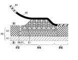
以下、図1A及び図1Bを参照して、回路基板30(図5C参照)の作成に用いるシート材40の構成について説明する。図1Aは、シート材40の構造を示す図である。図1Bは、シート材40の熱膨張性層42(図1A参照)に用いる熱膨張性材料の構造を示す図である。図1Bは、図1Aの熱膨張性層42の領域Arを拡大して示している。
<Structure of sheet material used for making circuit boards>
Hereinafter, the configuration of the
図1Aに示すように、シート材40は、基材層41(基材)の上に、熱膨張性層42と、マイクロフィルム44と、を備えている。
As shown in FIG. 1A, the
基材層41(基材)は、紙や、PET(polyethylene terephthalate)等の樹脂で構成されている。基材層41は、好ましくは、耐熱性を有するとよい。また、基材層41は、好ましくは、適度な可撓性を有するとよい。
熱膨張性層42は、加熱されることで膨張する層である。
マイクロフィルム44は、光熱変換用インク45(図2A参照)が印刷(塗布)される層である。
The base material layer 41 (base material) is made of paper or a resin such as PET (polyethylene terephthalate). The
The heat-
The
図1Bに示すように、熱膨張性層42には、熱膨張性材料である熱膨張性インク50が用いられている。熱膨張性層42は、例えば、基材層41の上に、熱膨張性材料である液状の熱膨張性インク50を塗布して乾燥させることで形成される。
As shown in FIG. 1B, a heat-
熱膨張性インク50(熱膨張性材料)は、導電性を有するバインダー56に絶縁性を有するマイクロカプセル51が混入された構成になっている。熱膨張性層42は、マイクロフィルム44に光熱変換用インク45(図2A参照)が印刷(塗布)されることで、光がシート材40に照射されたときに、その印刷領域が膨張する。
The heat-expandable ink 50 (heat-expandable material) has a structure in which a
バインダー56は、樹脂材のエマルジョンで構成されている。エマルジョンは、分散媒も分散質もともに液状になっている物質である。バインダー56は、導電性成分としての金属フィラー57を含有する。 The binder 56 is composed of an emulsion of a resin material. An emulsion is a substance in which both the dispersion medium and the dispersoid are liquid. The binder 56 contains a metal filler 57 as a conductive component.
マイクロカプセル51は、シェル52と、シェル52に内包された熱膨張性成分としてのコア53と、を有している。図1Bでは、手前側のシェル52の約4分の1がカットされ、内包されたコア53が示されている。シェル52は、例えば、熱可塑性樹脂であるアクリルニトリルコポリマーで構成されている。シェル52は、絶縁性を有している。シェル52に内包されたコア53は、炭化水素54によって構成されており、絶縁性を有している。炭化水素54は、加熱されることで膨張する熱膨張性を有している。
The
なお、前記した「熱可塑性」とは、押圧されながら加熱されることで塑性変形する特性を意味している。また、前記した「熱膨張性」とは、加熱されることで膨張する特性を意味している。 The above-mentioned "thermoplasticity" means a property of being plastically deformed by being heated while being pressed. Further, the above-mentioned "thermally expandable property" means a property of expanding by being heated.
炭化水素54は、好ましくは、液状で、比較的沸点が低いもの(液状低沸点炭化水素)がよい。炭化水素54の成分としては、例えば、炭素の個数が少ないものから順に、以下のものがある。 The hydrocarbon 54 is preferably liquid and has a relatively low boiling point (liquid low boiling point hydrocarbon). Examples of the components of the hydrocarbon 54 include the following in order from the one having the smallest number of carbons.
メタン(CH4)、エタン(C2H6)、プロパン(C3H8)、ブタン(C4H10)、ペンタン(C5H12)、ヘキサン(C6H14)、ヘプタン(C7H16)、オクタン(C8H18)、ノナン(C9H20)、デカン(C10H22)。 Methane (CH 4 ), Etan (C 2 H 6 ), Propane (C 3 H 8 ), Butane (C 4 H 10 ), Pentane (C 5 H 12 ), Hexane (C 6 H 14 ), Heptan (C 7 H 16 ), octane (C 8 H 18 ), nonane (C 9 H 20 ), decane (C 10 H 22 ).
炭化水素54の沸点は、炭素の個数が多いものほど高くなる。一例として、前記した各成分の沸点は以下の通りである。 The boiling point of the hydrocarbon 54 increases as the number of carbon atoms increases. As an example, the boiling points of the above-mentioned components are as follows.
メタンは−162℃、エタンは−89℃、プロパンは−42℃、ブタンは−1℃、ペンタンは36.1℃、ヘキサンは68℃、ヘプタンは98.42℃、オクタンは125℃、ノナンは151℃、デカンは174.1℃である。 Methane is -162 ° C, ethane is -89 ° C, propane is -42 ° C, butane is -1 ° C, pentane is 36.1 ° C, hexane is 68 ° C, heptane is 98.42 ° C, octane is 125 ° C, nonane is 151 ° C. and decane are 174.1 ° C.
本実施形態では、炭化水素54は、所望の温度(膨張温度)で膨張するように、これらの成分を単体で用いたり、又は、2種類以上の成分を用いてそれらを混合させたりして構成されている。 In the present embodiment, the hydrocarbon 54 is configured by using these components alone or by mixing them with two or more kinds of components so as to expand at a desired temperature (expansion temperature). Has been done.
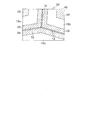
マイクロカプセル51のコア53は、加熱されることで膨張する。マイクロカプセル51のシェル52は、コア53(熱膨張性成分)の膨張に伴って延びるように変形する。シェル52は、絶縁性を有するため、コア53(熱膨張性成分)の膨張に伴って変形することで、他のカプセルと接触して、他のカプセルとの間で絶縁領域を形成する。
The
<回路基板の形成工程>
以下、図2A乃至図2Dを参照して、回路基板30の形成工程について説明する。図2A乃至図2Dは、それぞれ、シート材40の断面形状の変化によって、回路基板30の形成工程を示す図である。
<Circuit board forming process>
Hereinafter, the process of forming the
図2Aに示すように、シート材40の全領域は、導電領域となっている。作成者は、シート材40をインクジェット方式の図示せぬプリンタにセットする。そして、作成者は、図示せぬプリンタで、マイクロフィルム44の熱膨張性層42を膨張させたい領域に光熱変換用インク45を印刷(塗布)する。本実施形態では、「熱膨張性層42を膨張させたい領域」とは、絶縁領域を形成する領域である。光熱変換用インク45は、カーボンブラックを含む黒色インクである。光熱変換用インク45は、光を吸収して吸収した光を熱に変換する。
As shown in FIG. 2A, the entire region of the
次に、図2Bに示すように、作成者は、光熱変換用インク45が印刷されたシート材40を加熱装置103(熱源)の近傍に配置して、加熱装置103から光を照射させる。加熱装置103(熱源)は、例えば、ハロゲンヒータによって構成される。シート材40は、加熱装置103から光が照射されると、光熱変換用インク45で光を熱に変換する。すると、光熱変換用インク45が印刷された領域の下方で、熱膨張性層42が熱に反応して部分的に膨張する。これにより、シート材40に膨張領域が形成される。
Next, as shown in FIG. 2B, the creator arranges the
このとき、シート材40の膨張領域は絶縁領域となり、シート材40の非膨張領域が導電領域となる。このように層構造が変化する原理については、図3A乃至図3Cを参照して後記する。
At this time, the expanded region of the
次に、図2Cに示すように、作成者は、熱膨張性層42からマイクロフィルム44を引き剥がして除去する。これにより、図2Dに示すように、作成者は、熱膨張性層42を露出させる。
Next, as shown in FIG. 2C, the creator peels and removes the
作成者は、このようなシート材40を用いることによって、任意のパターンの絶縁領域を有する導電回路が形成された回路基板30を作成することができる。
By using such a
<層構造が変化する原理>
ところで、シート材40の熱膨張性層42は、膨張前と膨張途中と膨張後とで図3A乃至図3Cに示すように層構造が変化する。図3Aは、熱膨張性層42を膨張させたい領域における膨張前の状態を示す図である。図3Bは、熱膨張性層42を膨張させたい領域における膨張途中の状態を示す図である。図3Aは、熱膨張性層42を膨張させたい領域における膨張後の状態を示す図である。
<Principle of changing layer structure>
By the way, the layer structure of the heat-
図3Aに示すように、熱膨張性層42の膨張前において、熱膨張性層42を膨張させたい領域では、熱膨張性層42に混入されたマイクロカプセル51の全部が膨張しない状態になっている。そのため、大半のマイクロカプセル51のシェル52が他のカプセルと接触しない状態になっている。この状態において、十分な量の導電性のバインダー56が、大半のマイクロカプセル51の周囲に存在している。そのため、熱膨張性層42を膨張させたい領域は、導電領域となっている。
As shown in FIG. 3A, before the expansion of the
図3Bに示すように、熱膨張性層42の膨張途中において、熱膨張性層42を膨張させたい領域では、熱膨張性層42に混入されたマイクロカプセル51のごく一部が膨張している。そのため、一部のマイクロカプセル51のシェル52が他のカプセルと接触しているものの、大半のマイクロカプセル51のシェル52が他のカプセルと接触しない状態になっている。この状態において、まだ十分な量の導電性のバインダー56が、大半のマイクロカプセル51の周囲には存在している。そのため、熱膨張性層42を膨張させたい領域は、まだ導電領域となっている。
As shown in FIG. 3B, in the region where the
図3Cに示すように、熱膨張性層42の膨張後において、熱膨張性層42の膨張領域では、熱膨張性層42に混入されたマイクロカプセル51の一部(又は、全部)が膨張している。そのため、大半のマイクロカプセル51のシェル52が他のカプセルと接触した状態になっている。この状態において、少量の導電性のバインダー56しか、各マイクロカプセル51の周囲に存在していない。そして、絶縁性のシェル52が、他のカプセルと接触して、他のカプセルとの間で導通している。そのため、熱膨張性層42の膨張領域は、絶縁領域となっている。なお、熱膨張性層42の膨張領域は、好ましくは、弾性を有しているとよい。
As shown in FIG. 3C, after the expansion of the heat-
<変換図の作成>
回路基板30(図5C参照)の作成者は、例えば、予め設計された電子回路図10(図4B参照)の電子回路図データD10(図4B参照)を用意する。作成者は、運用に応じて、様々なパターンの電子回路図10(図4B参照)を設計することができる。そして、作成者は、回路基板30(図5C参照)の作成に際して、例えば、図4Aに示すコンピュータ101を変換図作成装置として機能させることで電子回路図10(図4B参照)に対応する変換図20(図4C参照)を示す変換図データD20を作成させる。変換図20は、光熱変換用インク45で形成される画像を示す図である。図4Aは、変換図作成装置の一例を示す図である。また、図4B及び図4Cは、入力画面IMの一例を示す図である。
<Creation of conversion diagram>
The creator of the circuit board 30 (see FIG. 5C) prepares, for example, the electronic circuit diagram data D10 (see FIG. 4B) of the electronic circuit diagram 10 (see FIG. 4B) designed in advance. The creator can design various patterns of electronic circuit diagrams 10 (see FIG. 4B) depending on the operation. Then, when creating the circuit board 30 (see FIG. 5C), the creator causes, for example, the
図4Bに示す例では、電子回路図データD10の電子回路図10は、導電領域13の中に絶縁領域Brが設けられた回路11を示している。図4Bに示す例では、入力画面IMは、絶縁性を有する絶縁性インクで形成される後記する保護膜29(図6C参照)の領域を設定するための「設定」ボタンや、電子回路図10から変換図20(図4C参照)を作成するための「変換」ボタンを含む構成になっている。
In the example shown in FIG. 4B, the electronic circuit diagram 10 of the electronic circuit diagram data D10 shows a
図4Aに示すように、変換図作成装置としてのコンピュータ101は、CPU101aと、記憶部101bと、表示部101cと、入力部101dと、を備えている。記憶部101bには、電子回路図10から変換図20(図4C参照)を作成するための制御プログラムPr101が予めインストールされている。コンピュータ101は、制御プログラムPr101に従って、電子回路図10(図4B参照)から変換図20(図4C参照)を作成する。作成者は、例えば、図4Bに示すように、入力画面IMに電子回路図10を表示させて「変換」ボタンを押下することで、コンピュータ101に変換図20(図4C参照)を作成させる。
As shown in FIG. 4A, the
図4Cに示すように、変換図データD20の変換図20は、絶縁領域12(図5C参照)を形成するために光熱変換用インク45で形成される画像を示している。絶縁領域12(図5C参照)の線幅(太さ)や、厚さ(濃度)は、光熱変換用インク45で形成される画像の線幅(太さ)や、厚さ(濃度)によって規定される。図4Cに示す例では、入力画面IMは、変換図20における任意の領域Ar1,Ar2,Ar2を指定してそれらの太さを任意の値に設定することができる構成になっている。
As shown in FIG. 4C, the conversion diagram 20 of the conversion diagram data D20 shows an image formed by the
<回路基板の作成>
以下、図5A乃至図5Cを参照して、回路基板30の作成について説明する。図5A乃至図5Cは、それぞれ、回路基板30の作成例を示す説明図である。
<Creation of circuit board>
Hereinafter, the production of the
図5Aに示す例では、シート材40の表面の全面に、導電領域13が形成されている。作成者は、シート材40を図示せぬプリンタにセットする。そして、図5Bに示すように、作成者は、図示せぬプリンタで、熱膨張性層42(図2A参照)を膨張させたい領域に光熱変換用インク45を印刷(塗布)する。
In the example shown in FIG. 5A, the
次に、作成者は、シート材40を加熱装置103(図2B参照)にセットし、加熱装置103(図2B参照)から光をシート材40に照射させる。このとき、シート材40の光熱変換用インク45が光を熱に変換する。これにより、光熱変換用インク45の印刷部分(図5B参照)が発熱する。その結果、図5Cに示すように、シート材40の熱膨張性層42(図2B参照)が部分的に膨張して、シート材40に立体的な絶縁領域12が形成される。この後、作成者は、熱膨張性層42からマイクロフィルム44を引き剥がして(図2C参照)、熱膨張性層42を露出させる(図2D参照)。これにより、回路基板30が作成される。
Next, the creator sets the
このような回路基板30は、所望領域を膨張させて絶縁領域12を形成することで、動作回路を構成することができる。回路基板30は、例えば、フレキシブル配線基板やユニバーサル基板と同程度の配線機能を有している。
Such a
作成者は、回路11が作成されたシート材40を回路基板30として用いることができる。また、作成者は、シート材40から任意の部分を切り離すことで、様々な形状の回路基板30を作成することもできる。
The creator can use the
ところで、図5Cに示す例では、回路11は、導電領域13(導電領域13a,13b,13c)の全面が剥き出しの構成になっている。そのため、回路11は、好ましくは、金属等を導電領域13に載せたときに、導電領域13が短絡(ショート)しないようにするとよい。そこで、例えば、図6Aに示すように、回路11は、好ましくは、導電領域13の中に後記する保護膜29(図6C参照)で保護される保護領域Prを設けるようにするとよい。図6Aは、保護領域Prが設定された電子回路図10の一例を示す説明図である。
By the way, in the example shown in FIG. 5C, the
なお、図6Aに示す例では、回路11は、保護領域Prが設けられずに、導電領域13の一部が剥き出しの構成になっている。しかしながら、回路11は、導電領域13の剥き出し部分が無くなるように、絶縁領域Br以外の導電領域13の全面に保護領域Prを設けるようにしてもよい。なお、導電領域13が剥き出しになっている部分は、例えば、接続端子として利用することができる。
In the example shown in FIG. 6A, the
作業者は、例えば、図6Aに示すように、入力画面IMに電子回路図10を表示させて「変換」ボタンを押下することで、コンピュータ101に変換図20(図6B参照)を作成させる。図6Bは、保護領域Prが設定された電子回路図10に対応する変換図20の説明図である。
For example, as shown in FIG. 6A, the operator causes the
図6Bに示すように、変換図データD20の変換図20は、保護領域Prに対応する保護膜29を形成するために絶縁性インクで形成される画像を示している。保護膜29の線幅(太さ)や、厚さ(濃度)は、絶縁性インクで形成される画像の線幅(太さ)や、厚さ(濃度)によって規定される。図6Bに示す例では、入力画面IMは、変換図20における任意の保護領域Pr1,Pr2,Pr3,Pr4,Pr5を指定してそれらの厚さを任意の値に設定することができる構成になっている。
As shown in FIG. 6B, the conversion diagram 20 of the conversion diagram data D20 shows an image formed of the insulating ink to form the
作成者は、図5Cのシート材40を図示せぬプリンタにセットする。そして、作成者は、図示せぬプリンタで、保護領域Pr1,Pr2,Pr3,Pr4,Pr5(図6B参照)に絶縁性インクを印刷(塗布)する。これにより、図6Cに示すように、導電領域13(導電領域13a,13b,13c)に保護膜29が形成された回路基板30が作成される。図6Cは、保護領域Prが設定された電子回路図10に対応する回路基板30の説明図である。
The creator sets the
<シート材と回路基板の主な特徴>
本実施形態に係るシート材40は、基材層41と、基材層41の上に形成された熱膨張性層42と、を備えている。熱膨張性層42は、マイクロカプセル51と、導電性を有するバインダー56と、を含んでいる。マイクロカプセル51は、絶縁性を有するシェル52と、シェル52に内包され、かつ、加熱されることで膨張する熱膨張性成分(コア53)と、を有している。シェル52は、熱膨張性成分(コア53)の膨張に伴って変形することで、他のカプセルと接触して、他のカプセルとの間で絶縁領域を形成する。
<Main features of sheet material and circuit board>
The
本実施形態に係る回路基板30は、このようなシート材40を部分的に膨張させることで形成される。本実施形態に係る回路基板30において、熱膨張性層42の非膨張領域は、回路11の導電領域を形成している。また、熱膨張性層42の膨張領域は、回路11の絶縁領域を形成している。このような回路基板30は、フレキシブル配線基板やユニバーサル基板と同程度の配線機能を有している。
The
また、回路基板30は、変換図20に対応する所望パターンをシート材40の上に光熱変換用インク45で印刷して、シート材40を部分的に膨張させるだけで作成することができる。このような回路基板30は、低額な材料で作成することができるため、安価に作成することができる。また、回路基板30は、短時間で容易に作成することができる。
Further, the
また、回路基板30は、設備として、専用の機械を用いなくても、汎用品(例えば、コンピュータ101(図4A参照)やプリンタ(図示せず)、加熱装置103(図2B参照)等)を用いるだけで、作成することができる。そのため、回路基板30は、作成コストを抑制することができる。
Further, the
また、回路基板30は、半田付け等の作業を要することなく作成することができる。そのため、回路基板30は、作成に際して、作成者の負担を軽減することができる。また、回路基板30は、短時間で大量に作成することができる。
Further, the
また、作成者は、回路基板30が安価なものであるため、例えば複数種類の回路基板30を少量ずつ作成することができる。そのため、作成者は、例えば開発中の製品に用いる回路の試作品として、複数種類の回路基板30を作成し、作成された各回路基板30を用いて様々なテストを行うこともできる。
Further, since the
また、回路基板30の絶縁領域12(図5C参照)の線幅(太さ)や、厚さ(濃度)は、光熱変換用インク45で形成される画像の線幅(太さ)や、厚さ(濃度)によって規定される。このような回路基板30は、光熱変換用インク45で形成される画像の線幅(太さ)や、厚さ(印刷濃度)で、絶縁程度を変えることができる。
The line width (thickness) and thickness (density) of the insulating region 12 (see FIG. 5C) of the
また、回路基板30は、熱膨張性層42の膨張領域の膨張高さに応じて絶縁程度が変わる。つまり、回路基板30は、絶縁程度が変わっていることが膨張領域の膨張高さで分かる構造になっている。このような回路基板30は、例えば、作成者が膨張領域を手で触った触感で絶縁程度の変化を認識することが可能な構造になっている。つまり、回路基板30は、視覚以外に、手で触った触感で、絶縁程度の変化を認識することが可能な構造になっている。
Further, the degree of insulation of the
また、回路基板30は、膨張領域の膨張高さ(つまり、光熱変換用インク45で形成される画像の印刷濃度)で絶縁程度を変えることができるため、これによって導電領域の表面抵抗値をある程度変えることもできる。
Further, since the degree of insulation of the
また、回路基板30は、回路11を一旦作成した後に、光熱変換用インク45を印刷して再度部分的に膨張させることで、元の回路11から別の回路に変更したり、元の回路11の構成が分からなくなるように変更したり(つまり、元の回路11を新たな膨張領域に埋没させて消去したり)することができる。そのため、回路基板30は、例えば、工場出荷前に、作成された回路11で様々なテストを行い、工場出荷時に、元の回路11から別の回路に変更したり、元の回路11の構成が分からなくなるように変更したりすることができる。このような回路基板30は、回路11の秘匿性を向上させることができる。
Further, the
また、回路基板30は、主に、紙や、PET等の樹脂で構成されているので、安全性が高い。そのため、回路基板30は、子供向けの科学教材や、理科の教材、工作用品等に利用することができる。
Further, since the
以上の通り、本実施形態に係るシート材40によれば、フレキシブル配線基板やユニバーサル基板と同程度の配線機能を有し、安価で作成時間が短く作成の容易な回路基板30を提供することができる。
As described above, according to the
なお、本発明は、前記した実施形態に限定されるものではなく、本発明の要旨を逸脱しない範囲で種々の変更や変形を行うことができる。 The present invention is not limited to the above-described embodiment, and various modifications and modifications can be made without departing from the gist of the present invention.
例えば、前記した実施形態は、本発明の要旨を分かり易く説明するために詳細に説明したものである。そのため、本発明は、必ずしも説明した全ての構成要素を備えるものに限定されるものではない。また、本発明は、ある構成要素に他の構成要素を追加したり、一部の構成要素を他の構成要素に変更したりすることができる。また、本発明は、一部の構成要素を削除することもできる。 For example, the above-described embodiment has been described in detail in order to explain the gist of the present invention in an easy-to-understand manner. Therefore, the present invention is not necessarily limited to those including all the components described above. In addition, the present invention can add other components to a certain component, or change some components to other components. In addition, the present invention can also delete some components.
例えば、図1Aに示すシート材40を用いることで、図7A乃至図7Cに示す電子装置80を提供作成することができる。図7A乃至図7Cは、それぞれ、シート材40を用いた電子装置80の説明図である。ここでは、電子装置80が、例えばスマートフォン等のモバイル装置に接続されて、モバイル装置に電力を供給するバッテリー装置である場合を想定して説明する。
For example, by using the
図7Aに示す例では、電子装置80は、ケース81の内部に、電解質の溶液が充填されたタンク82を備えている。タンク82の周囲は、シート材40で覆われている。ここで、仮に、例えば図7Bに示すように、タンク82が破損して、タンク82から溶液が漏れ出たものとする。そして、タンク82は、漏れ出した溶液によりタンク82の破損個所付近で電流が流れて、意図せぬ短絡(ショート)が発生し、破損個所付近でシート材40の膨張温度以上の熱が発生したものとする。
In the example shown in FIG. 7A, the
この場合に、図7Cに示すように、破損個所付近でシート材40が膨張する。これにより、シート材40は、タンク82の破損個所付近を閉鎖して、溶液の漏れを抑制する。また、シート材40の膨張領域は、絶縁領域である。そのため、シート材40の膨張領域は、漏れ出した溶液による短絡(ショート)の発生を抑制して、破損個所付近の温度を低下させる。このような電子装置80は、万が一破損が発生しても、装置の安全性を向上させることができる。
In this case, as shown in FIG. 7C, the
なお、電子装置80は、バッテリー装置に限らず、発熱が想定される箇所をシート材40で覆う構成であれば、他の装置であってもよい。また、電子装置80は、発熱が想定される箇所に熱膨張性インク50(熱膨張性材料)を塗布したものであってもよい。また、シート材40は、例えば、火災報知機の温度センサや電子装置80のヒューズを覆うようにしてもよい。
The
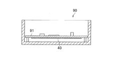
また、例えば、図1Aに示すシート材40を用いることで、図8A乃至図8Cに示す発熱箇所解析構造90を提供作成することができる。図8A乃至図8Cは、それぞれ、シート材40を用いた発熱箇所解析構造90の説明図である。ここでは、発熱箇所解析構造90の適用装置がデスクトップ型のコンピュータであり、発熱箇所の解析対象が回路基板91である場合を想定して説明する。
Further, for example, by using the
図8Aに示す例では、発熱箇所解析構造90の適用装置であるコンピュータの内部には、回路基板91が配置され、その下部にシート材40が配置されている。ここで、仮に、回路基板91で、シート材40の膨張温度以上の熱が発生したものとする。この場合に、図8Bに示すように、発熱箇所付近でシート材40が膨張して、膨張箇所49が形成される。このような場合に、解析者は、図8Cに示すように、装置からシート材40を取り外して、シート材40の膨張箇所49を確認することで、解析対象(回路基板91)のどの部位で熱が発生したのかを解析することができる。
In the example shown in FIG. 8A, the
なお、シート材40は、好ましくは、膨張温度の異なる複数種類の熱膨張性層42(図1A)が積層された構造であるとよい。これにより、発熱箇所解析構造90は、解析対象(回路基板91)のどの部位がどの程度の温度に達したのかを解析することができる。また、発熱箇所解析構造90は、シート材40の膨張箇所49が複数階の層状になるため、解析対象(回路基板91)の中で熱がどのように伝播したのかを解析することができる。
The
なお、従来は、仮に解析対象(回路基板91)で不具合が発生して発熱する場合があったとしても、その現象を再現することができないことがあった。これに対して、本発明に係る発熱箇所解析構造90は、解析対象(回路基板91)の発熱箇所の痕跡を目視可能な状態で残すことができる。そのため、本発明に係る発熱箇所解析構造90は、解析対象(回路基板91)の不具合を解析し易くすることができる。
In the past, even if a problem occurred in the analysis target (circuit board 91) and heat was generated, that phenomenon could not be reproduced. On the other hand, the heat generation
以下に、この出願の願書に最初に添付した特許請求の範囲に記載した発明を付記する。付記に記載した請求項の項番は、この出願の願書に最初に添付した特許請求の範囲の通りである。
[付記]
《請求項1》
基材層と、
前記基材層の上に形成された熱膨張性層と、を備え、
前記熱膨張性層は、マイクロカプセルと、導電性を有するバインダーと、を含み、
前記マイクロカプセルは、絶縁性を有するシェルと、前記シェルに内包され、かつ、加熱されることで膨張する熱膨張性成分と、を有し、
前記シェルは、前記熱膨張性成分の膨張に伴って絶縁領域を形成する、
ことを特徴とするシート材。
《請求項2》
請求項1に記載のシート材を部分的に膨張させることによって形成され、
前記熱膨張性層の非膨張領域は、回路の導電領域を形成し、
前記熱膨張性層の膨張領域は、回路の絶縁領域を形成している、
ことを特徴とする回路基板。
《請求項3》
前記熱膨張性層の非膨張領域の一部又は全ての上に、絶縁性を有する絶縁性インクで保護膜が形成されている、
ことを特徴とする請求項2に記載の回路基板。
《請求項4》
前記熱膨張性層は、膨張温度の異なる複数種類の前記マイクロカプセルで構成された複数の層が積層されている、
ことを特徴とする請求項2に記載の回路基板。
《請求項5》
コンピュータに、
予め用意された電子回路図データに基づいて、前記電子回路図データに含まれる絶縁領域の一部又は全てが回路基板を構成するシート材に含まれている熱膨張性層の膨張領域に変換された変換図データを作成させる、
ことを特徴とするプログラム。
《請求項6》
コンピュータに、
前記電子回路図データに含まれる絶縁領域の太さに応じて、前記膨張領域の太さを決定させる、
ことを特徴とする請求項5に記載のプログラム。
《請求項7》
コンピュータに、
前記電子回路図データに基づいて、絶縁性を有する絶縁性インクで形成される保護膜の領域を決定させる、
ことを特徴とする請求項5に記載のプログラム。
《請求項8》
絶縁性を有するシェルと、前記シェルに内包され、かつ、加熱されることで膨張する熱膨張性成分と、を有するマイクロカプセルを、電流が流れる部分の周囲に配置しておき、
意図せぬ短絡箇所の発生時に、短絡により発生する熱で前記マイクロカプセルを膨張させて、短絡箇所の周囲を絶縁させる、
ことを特徴とする電子装置。
《請求項9》
シェルと、前記シェルに内包され、かつ、加熱されることで膨張する熱膨張性成分と、を有するマイクロカプセルを、製品の任意の箇所に配置しておき、
前記マイクロカプセルの膨張領域が発生している場合に、その膨張領域を解析することで製品の意図せぬ発熱箇所の解析を可能にする、
ことを特徴とする発熱箇所解析構造。
The inventions described in the claims originally attached to the application of this application are added below. The claims in the appendix are as specified in the claims originally attached to the application for this application.
[Additional Notes]
<< Claim 1 >>
Base layer and
A thermally expandable layer formed on the base material layer is provided.
The thermally expandable layer contains microcapsules and a conductive binder.
The microcapsules have an insulating shell and a heat-expandable component that is contained in the shell and expands when heated.
The shell forms an insulating region as the thermally expandable component expands.
A sheet material characterized by that.
<< Claim 2 >>
Formed by partially expanding the sheet material according to claim 1.
The non-expandable region of the thermally expandable layer forms a conductive region of the circuit.
The expansion region of the thermally expandable layer forms an insulating region of the circuit.
A circuit board characterized by that.
<< Claim 3 >>
A protective film is formed on a part or all of the non-expandable region of the heat-expandable layer with an insulating ink having an insulating property.
The circuit board according to claim 2.
<< Claim 4 >>
The thermally expandable layer is formed by laminating a plurality of layers composed of a plurality of types of the microcapsules having different expansion temperatures.
The circuit board according to claim 2.
<< Claim 5 >>
On the computer
Based on the electronic circuit diagram data prepared in advance, a part or all of the insulating region included in the electronic circuit diagram data is converted into an expansion region of the thermally expandable layer included in the sheet material constituting the circuit board. Create conversion diagram data
A program characterized by that.
<< Claim 6 >>
On the computer
The thickness of the expansion region is determined according to the thickness of the insulation region included in the electronic circuit diagram data.
The program according to claim 5, wherein the program is characterized by the above.
<< Claim 7 >>
On the computer
Based on the electronic circuit diagram data, the region of the protective film formed of the insulating ink having an insulating property is determined.
The program according to claim 5, wherein the program is characterized by the above.
<< Claim 8 >>
A microcapsule having an insulating shell and a heat-expandable component contained in the shell and expanded by heating is arranged around a portion through which an electric current flows.
When an unintended short circuit occurs, the heat generated by the short circuit expands the microcapsules to insulate the periphery of the short circuit.
An electronic device characterized by that.
<< Claim 9 >>
A microcapsule having a shell and a heat-expandable component contained in the shell and expanding by heating is placed at an arbitrary position in the product.
When an expansion region of the microcapsule is generated, it is possible to analyze an unintended heat generation portion of the product by analyzing the expansion region.
A heat generation location analysis structure characterized by this.
D10 電子回路図データ
D20 変換図データ
10 電子回路図
11 回路
12 絶縁領域
13,13a,13b,13c 導電領域
29 保護膜
30 回路基板
40 シート材
41 基材層(基材)
42 熱膨張性層
44 マイクロフィルム
45 光熱変換用インク(カーボンブラックを含む黒色インク)
50 熱膨張性インク(熱膨張性材料)
51 マイクロカプセル(熱膨張性成分)
52 シェル
52a 外側層
52b 内側層
53 コア(熱膨張性成分)
54 炭化水素(液状低沸点炭化水素)
56 バインダー
57 金属フィラー(導電性成分)
D10 Electronic circuit diagram data D20
42
50 Thermally expandable ink (thermally expandable material)
51 Microcapsules (thermally expanding component)
52 Shell 52a Outer layer
54 Hydrocarbons (liquid low boiling point hydrocarbons)
56 Binder 57 Metal filler (conductive component)
Claims (3)
電子回路図データに基づいて、前記電子回路図データに含まれる絶縁領域の一部又は全てを、回路基板を構成するシート材に含まれている熱膨張性層を膨張させる光熱変換用インクで、画像として描かせるためのプログラム。Based on the electronic circuit diagram data, a part or all of the insulating region included in the electronic circuit diagram data is a photothermal conversion ink that expands the heat-expandable layer contained in the sheet material constituting the circuit board. A program for drawing as an image.
前記電子回路図データに含まれる絶縁領域の太さに応じて、前記光熱変換用インクで描かれる画像の線の太さを決定させる、The thickness of the line of the image drawn by the photothermal conversion ink is determined according to the thickness of the insulating region included in the electronic circuit diagram data.
ことを特徴とする請求項1に記載のプログラム。The program according to claim 1, wherein the program is characterized by the above.
前記電子回路図データに基づいて、絶縁性を有する絶縁性インクで形成される保護膜の領域を決定させる、Based on the electronic circuit diagram data, the region of the protective film formed of the insulating ink having an insulating property is determined.
ことを特徴とする請求項1または2に記載のプログラム。The program according to claim 1 or 2.
Priority Applications (3)
| Application Number | Priority Date | Filing Date | Title |
|---|---|---|---|
| JP2018139792A JP6819657B2 (en) | 2018-07-25 | 2018-07-25 | program |
| US16/514,971 US10897817B2 (en) | 2018-07-25 | 2019-07-17 | Thermally expandable material, sheet material, circuit board, method for manufacturing circuit board, computer readable storage medium, electronic apparatus, and structure to analyze heat-generation position |
| CN201910665677.XA CN110785008A (en) | 2018-07-25 | 2019-07-23 | Thermally expandable material, sheet, circuit board and method for manufacturing same, storage medium, electronic device, and heat generation position analysis structure |
Applications Claiming Priority (1)
| Application Number | Priority Date | Filing Date | Title |
|---|---|---|---|
| JP2018139792A JP6819657B2 (en) | 2018-07-25 | 2018-07-25 | program |
Related Child Applications (1)
| Application Number | Title | Priority Date | Filing Date |
|---|---|---|---|
| JP2020213046A Division JP2021061421A (en) | 2020-12-23 | 2020-12-23 | program |
Publications (2)
| Publication Number | Publication Date |
|---|---|
| JP2020017636A JP2020017636A (en) | 2020-01-30 |
| JP6819657B2 true JP6819657B2 (en) | 2021-01-27 |
Family
ID=69177293
Family Applications (1)
| Application Number | Title | Priority Date | Filing Date |
|---|---|---|---|
| JP2018139792A Active JP6819657B2 (en) | 2018-07-25 | 2018-07-25 | program |
Country Status (3)
| Country | Link |
|---|---|
| US (1) | US10897817B2 (en) |
| JP (1) | JP6819657B2 (en) |
| CN (1) | CN110785008A (en) |
Families Citing this family (1)
| Publication number | Priority date | Publication date | Assignee | Title |
|---|---|---|---|---|
| CN112859448B (en) * | 2021-03-17 | 2023-03-14 | 重庆京东方显示照明有限公司 | Adhesive tape, backlight module, display device and preparation method of backlight module |
Family Cites Families (18)
| Publication number | Priority date | Publication date | Assignee | Title |
|---|---|---|---|---|
| JP3186835B2 (en) * | 1992-05-28 | 2001-07-11 | 松本油脂製薬株式会社 | Thermally expandable microcapsule, method for producing and expanding method |
| JP3103956B2 (en) * | 1993-06-03 | 2000-10-30 | ソニーケミカル株式会社 | Anisotropic conductive film |
| JP3409190B2 (en) * | 1993-06-17 | 2003-05-26 | ソニーケミカル株式会社 | Fuse resistor |
| JP3418430B2 (en) * | 1993-08-11 | 2003-06-23 | 日東電工株式会社 | Microcapsule processing method |
| JPH0825785A (en) | 1994-07-21 | 1996-01-30 | Brother Ind Ltd | Stereoscopic image forming sheet |
| US5834526A (en) * | 1997-07-11 | 1998-11-10 | Wu; Huey S. | Expandable hollow particles |
| EP1050888B1 (en) * | 1998-08-28 | 2010-10-06 | Panasonic Corporation | Conductive paste, conductive structure using the same, electronic part, module, circuit board, method for electrical connection, method for manufacturing circuit board, and method for manufacturing ceramic electronic part |
| JP3252183B2 (en) | 1999-02-03 | 2002-01-28 | カシオ計算機株式会社 | Flexible wiring board and method of manufacturing the same |
| JP2001042763A (en) | 1999-07-28 | 2001-02-16 | Hachiken Denshi:Kk | Electronic teaching materials |
| MXPA03010758A (en) * | 2001-05-25 | 2004-07-01 | Apache Prod Co | Foam insulation made with expandable microspheres and methods. |
| JP2006245238A (en) * | 2005-03-02 | 2006-09-14 | Canon Inc | Method for forming through hole and method for manufacturing electronic circuit |
| JP2007194069A (en) | 2006-01-19 | 2007-08-02 | Sony Corp | Current shut off mechanism and battery |
| JP2007273127A (en) * | 2006-03-30 | 2007-10-18 | Matsushita Electric Ind Co Ltd | Nonaqueous secondary battery |
| FR2901486A1 (en) * | 2006-05-24 | 2007-11-30 | Salomon Sa | ASSEMBLY COMPRISING A SLIDING BOARD AND A DEVICE FOR RETAINING A FOOTWEAR ARTICLE ON THE BOARD |
| JP2008269883A (en) * | 2007-04-18 | 2008-11-06 | Alps Electric Co Ltd | Fuse function element, its manufacturing method, circuit board using fuse function element, and its manufacturing method |
| JP2010146726A (en) * | 2007-11-30 | 2010-07-01 | Kyoritsu Kagaku Sangyo Kk | Conductive composition |
| JP2015024945A (en) * | 2013-07-29 | 2015-02-05 | サムソン エレクトロ−メカニックス カンパニーリミテッド. | Inorganic filler, and insulating resin composition, insulating film, prepreg and printed circuit board including the same |
| EP3324481A1 (en) * | 2016-11-21 | 2018-05-23 | TE Connectivity Nederland B.V. | Method for manufacturing a dielectric-filled metal waveguide |
-
2018
- 2018-07-25 JP JP2018139792A patent/JP6819657B2/en active Active
-
2019
- 2019-07-17 US US16/514,971 patent/US10897817B2/en active Active
- 2019-07-23 CN CN201910665677.XA patent/CN110785008A/en active Pending
Also Published As
| Publication number | Publication date |
|---|---|
| JP2020017636A (en) | 2020-01-30 |
| CN110785008A (en) | 2020-02-11 |
| US20200037445A1 (en) | 2020-01-30 |
| US10897817B2 (en) | 2021-01-19 |
Similar Documents
| Publication | Publication Date | Title |
|---|---|---|
| KR102035560B1 (en) | Arrangement and method for facilitating electronics design in connection with 3d structures | |
| JP6819657B2 (en) | program | |
| Yamaoka et al. | FoldTronics: Creating 3D objects with integrated electronics using foldable honeycomb structures | |
| US9504148B1 (en) | Rapid PCB prototyping by selective adhesion | |
| Lo et al. | ShrinkyCircuits: sketching, shrinking, and formgiving for electronic circuits | |
| JP6819656B2 (en) | Circuit board, program, and button structure | |
| CN105263263A (en) | Processing technology optimization method of ultrathin flexible plate | |
| JP2021061421A (en) | program | |
| EP3611649B1 (en) | Computer readable storage medium and method of forming electronic circuit diagram | |
| JP2021044597A (en) | Circuit board, program, and button structure | |
| CN113010960B (en) | Method and device for generating part manufacturing control data and computer equipment | |
| US11122690B2 (en) | Additive manufacturing techniques for meander-line polarizers | |
| JP2020025081A (en) | Program, conductive circuit and creation method of conversion figure used for creation of conductive circuit | |
| JP2020090041A (en) | Expansion device, shaping system, and method for manufacturing shaped object | |
| JP7014200B2 (en) | Model manufacturing method and expansion device | |
| Du et al. | Experiencing Visual Blocks for ML: Visual Prototyping of AI Pipelines | |
| JP6597841B2 (en) | Thermally expansible sheet, method for producing thermally expansible sheet, modeled object, and method for manufacturing modeled object | |
| CN206461842U (en) | Panel construction for making double-sided PCB board | |
| David et al. | Numerical Control Plotter For Direct-To-Blank Substrate Tracing Of Conductive Ink For Electronic Education Purposes | |
| JP2018047557A (en) | Stereo molded article production system, and program | |
| Zakai et al. | PCB Design and Fabrication | |
| CN107949163A (en) | A kind of thin film printed circuit board and processing method | |
| JP7263973B2 (en) | Molded object manufacturing method | |
| JP2979231B2 (en) | 3D image formation method | |
| CN206585850U (en) | One kind automation boat-carrying VDES apparatus casings |
Legal Events
| Date | Code | Title | Description |
|---|---|---|---|
| A621 | Written request for application examination |
Free format text: JAPANESE INTERMEDIATE CODE: A621 Effective date: 20200114 |
|
| A977 | Report on retrieval |
Free format text: JAPANESE INTERMEDIATE CODE: A971007 Effective date: 20200902 |
|
| A131 | Notification of reasons for refusal |
Free format text: JAPANESE INTERMEDIATE CODE: A131 Effective date: 20200908 |
|
| A521 | Written amendment |
Free format text: JAPANESE INTERMEDIATE CODE: A523 Effective date: 20201014 |
|
| TRDD | Decision of grant or rejection written | ||
| A01 | Written decision to grant a patent or to grant a registration (utility model) |
Free format text: JAPANESE INTERMEDIATE CODE: A01 Effective date: 20201201 |
|
| A61 | First payment of annual fees (during grant procedure) |
Free format text: JAPANESE INTERMEDIATE CODE: A61 Effective date: 20201214 |
|
| R150 | Certificate of patent or registration of utility model |
Ref document number: 6819657 Country of ref document: JP Free format text: JAPANESE INTERMEDIATE CODE: R150 |