JP6815030B2 - Circuit breaker - Google Patents
Circuit breaker Download PDFInfo
- Publication number
- JP6815030B2 JP6815030B2 JP2016566455A JP2016566455A JP6815030B2 JP 6815030 B2 JP6815030 B2 JP 6815030B2 JP 2016566455 A JP2016566455 A JP 2016566455A JP 2016566455 A JP2016566455 A JP 2016566455A JP 6815030 B2 JP6815030 B2 JP 6815030B2
- Authority
- JP
- Japan
- Prior art keywords
- circuit breaker
- current
- inductor
- semiconductor
- capacitor
- Prior art date
- Legal status (The legal status is an assumption and is not a legal conclusion. Google has not performed a legal analysis and makes no representation as to the accuracy of the status listed.)
- Active
Links
- 239000004065 semiconductor Substances 0.000 claims description 362
- 239000003990 capacitor Substances 0.000 claims description 153
- 238000004146 energy storage Methods 0.000 claims description 56
- HEZMWWAKWCSUCB-PHDIDXHHSA-N (3R,4R)-3,4-dihydroxycyclohexa-1,5-diene-1-carboxylic acid Chemical compound O[C@@H]1C=CC(C(O)=O)=C[C@H]1O HEZMWWAKWCSUCB-PHDIDXHHSA-N 0.000 claims description 49
- 238000001514 detection method Methods 0.000 claims description 44
- 238000006243 chemical reaction Methods 0.000 claims description 40
- 230000004044 response Effects 0.000 claims description 22
- 230000000903 blocking effect Effects 0.000 claims description 14
- 238000009825 accumulation Methods 0.000 claims 6
- 238000010586 diagram Methods 0.000 description 54
- 230000004048 modification Effects 0.000 description 47
- 238000012986 modification Methods 0.000 description 47
- 238000004088 simulation Methods 0.000 description 46
- 238000000034 method Methods 0.000 description 12
- 238000007599 discharging Methods 0.000 description 9
- 230000008901 benefit Effects 0.000 description 6
- 230000001172 regenerating effect Effects 0.000 description 6
- 230000009467 reduction Effects 0.000 description 5
- 230000008859 change Effects 0.000 description 4
- WABPQHHGFIMREM-UHFFFAOYSA-N lead(0) Chemical compound [Pb] WABPQHHGFIMREM-UHFFFAOYSA-N 0.000 description 4
- 230000008569 process Effects 0.000 description 4
- 230000007423 decrease Effects 0.000 description 3
- 230000002411 adverse Effects 0.000 description 2
- 230000005540 biological transmission Effects 0.000 description 2
- 238000009434 installation Methods 0.000 description 2
- 230000010363 phase shift Effects 0.000 description 2
- 238000012360 testing method Methods 0.000 description 2
- 101100499229 Mus musculus Dhrsx gene Proteins 0.000 description 1
- 241000577979 Peromyscus spicilegus Species 0.000 description 1
- 235000001537 Ribes X gardonianum Nutrition 0.000 description 1
- 235000001535 Ribes X utile Nutrition 0.000 description 1
- 235000016919 Ribes petraeum Nutrition 0.000 description 1
- 244000281247 Ribes rubrum Species 0.000 description 1
- 235000002355 Ribes spicatum Nutrition 0.000 description 1
- 230000004888 barrier function Effects 0.000 description 1
- 238000011161 development Methods 0.000 description 1
- 230000000694 effects Effects 0.000 description 1
- 230000006872 improvement Effects 0.000 description 1
- 229910044991 metal oxide Inorganic materials 0.000 description 1
- 150000004706 metal oxides Chemical class 0.000 description 1
- 238000010248 power generation Methods 0.000 description 1
- 238000012545 processing Methods 0.000 description 1
- 239000007787 solid Substances 0.000 description 1
- 230000001629 suppression Effects 0.000 description 1
- 238000012546 transfer Methods 0.000 description 1
Images


Classifications
-
- H—ELECTRICITY
- H01—ELECTRIC ELEMENTS
- H01H—ELECTRIC SWITCHES; RELAYS; SELECTORS; EMERGENCY PROTECTIVE DEVICES
- H01H33/00—High-tension or heavy-current switches with arc-extinguishing or arc-preventing means
- H01H33/02—Details
- H01H33/59—Circuit arrangements not adapted to a particular application of the switch and not otherwise provided for, e.g. for ensuring operation of the switch at a predetermined point in the AC cycle
- H01H33/596—Circuit arrangements not adapted to a particular application of the switch and not otherwise provided for, e.g. for ensuring operation of the switch at a predetermined point in the AC cycle for interrupting DC
-
- H—ELECTRICITY
- H01—ELECTRIC ELEMENTS
- H01H—ELECTRIC SWITCHES; RELAYS; SELECTORS; EMERGENCY PROTECTIVE DEVICES
- H01H9/00—Details of switching devices, not covered by groups H01H1/00 - H01H7/00
- H01H9/54—Circuit arrangements not adapted to a particular application of the switching device and for which no provision exists elsewhere
- H01H9/541—Contacts shunted by semiconductor devices
- H01H9/542—Contacts shunted by static switch means
- H01H2009/543—Contacts shunted by static switch means third parallel branch comprising an energy absorber, e.g. MOV, PTC, Zener
-
- H—ELECTRICITY
- H02—GENERATION; CONVERSION OR DISTRIBUTION OF ELECTRIC POWER
- H02H—EMERGENCY PROTECTIVE CIRCUIT ARRANGEMENTS
- H02H3/00—Emergency protective circuit arrangements for automatic disconnection directly responsive to an undesired change from normal electric working condition with or without subsequent reconnection ; integrated protection
- H02H3/02—Details
- H02H3/021—Details concerning the disconnection itself, e.g. at a particular instant, particularly at zero value of current, disconnection in a predetermined order
-
- H—ELECTRICITY
- H02—GENERATION; CONVERSION OR DISTRIBUTION OF ELECTRIC POWER
- H02H—EMERGENCY PROTECTIVE CIRCUIT ARRANGEMENTS
- H02H3/00—Emergency protective circuit arrangements for automatic disconnection directly responsive to an undesired change from normal electric working condition with or without subsequent reconnection ; integrated protection
- H02H3/08—Emergency protective circuit arrangements for automatic disconnection directly responsive to an undesired change from normal electric working condition with or without subsequent reconnection ; integrated protection responsive to excess current
- H02H3/087—Emergency protective circuit arrangements for automatic disconnection directly responsive to an undesired change from normal electric working condition with or without subsequent reconnection ; integrated protection responsive to excess current for DC applications
-
- H—ELECTRICITY
- H03—ELECTRONIC CIRCUITRY
- H03K—PULSE TECHNIQUE
- H03K17/00—Electronic switching or gating, i.e. not by contact-making and –breaking
- H03K17/51—Electronic switching or gating, i.e. not by contact-making and –breaking characterised by the components used
- H03K2017/515—Mechanical switches; Electronic switches controlling mechanical switches, e.g. relais
Landscapes
- Engineering & Computer Science (AREA)
- Power Engineering (AREA)
- Emergency Protection Circuit Devices (AREA)
- Driving Mechanisms And Operating Circuits Of Arc-Extinguishing High-Tension Switches (AREA)
- Keying Circuit Devices (AREA)
Description
本発明は、地絡や短絡などの事故発生時に電流路を遮断する回路遮断器に関し、特に、機械スイッチ方式と半導体スイッチ方式とを併用したハイブリッド方式の回路遮断器に関する。 The present invention relates to a circuit breaker that cuts off a current path when an accident such as a ground fault or a short circuit occurs, and more particularly to a hybrid type circuit breaker that uses both a mechanical switch type and a semiconductor switch type.
近年、直流を用いた給電システムが注目されている。直流給電システムは、既存の交流給電システムと比較して変換器損失、送電損失および設置コストを低減できる利点がある。日本では、例えば、直流380[V]、変換器容量500[kW]クラスの直流給電システム、路面電車(600[V]、750[V])や直流電車(1000[V]、1500[V])用の直流給電システムなどが実用化されている。また、数10[kV]以上の高圧用途では、例えば将来の洋上風力発電システムの大量設置を想定し、電圧形変換器を用いた多端子直流送電システム(HVDC:high−voltage direct−current)の導入が期待されている。 In recent years, a power supply system using direct current has attracted attention. The DC power supply system has the advantage of reducing converter loss, transmission loss and installation cost as compared to existing AC power supply systems. In Japan, for example, DC 380 [V], converter capacity 500 [kW] class DC power supply system, tram (600 [V], 750 [V]) and DC train (1000 [V], 1500 [V] ) DC power supply system has been put into practical use. For high-voltage applications of several tens of [kV] or more, for example, assuming the large-scale installation of offshore wind power generation systems in the future, a multi-terminal DC transmission system (HVDC: high-voltage direct-current) using a voltage converter It is expected to be introduced.
直流給電システムにおいて地絡事故や短絡事故が発生した場合、過電流が発生する。事故発生からの電流の増加率([A/s])は、直流給電システムが有する直流インダクタンスに反比例する。例えば電圧形変換器を用いて直流電圧を生成した場合、直流インダクタンスが小さいため、過電流が生じる恐れがあるので、高速に動作可能な直流遮断器を設置する必要がある。 When a ground fault or short circuit accident occurs in a DC power supply system, an overcurrent occurs. The rate of increase in current ([A / s]) from the occurrence of an accident is inversely proportional to the DC inductance of the DC power supply system. For example, when a DC voltage is generated using a voltage converter, an overcurrent may occur because the DC inductance is small, so it is necessary to install a DC circuit breaker that can operate at high speed.
直流遮断器は、機械スイッチ方式、半導体スイッチ方式、およびハイブリッド方式の3種類に分類できる。 DC circuit breakers can be classified into three types: mechanical switch type, semiconductor switch type, and hybrid type.
このうち、機械スイッチ方式は、例えば、真空遮断器、ガス遮断器もしくは空気吹付遮断器などの機械的遮断器(サーキットブレーカ:Circuit Breaker)とLC共振回路とを用いて電流を遮断するものである(例えば、非特許文献1参照。)。機械スイッチ方式では、パワーデバイスを使用しないため定常損失は発生しない。
Of these, the mechanical switch system uses, for example, a mechanical circuit breaker (circuit breaker: Circuit Breaker) such as a vacuum circuit breaker, a gas circuit breaker, or an air blower circuit breaker, and an LC resonant circuit to cut off the current. (See, for example, Non-Patent
また、半導体スイッチ方式は、パワーデバイス(電力用半導体素子)を用いて遮断器を構成することで、高速な遮断時間(1[ms]以下)を実現する(例えば、非特許文献2参照。)。 Further, in the semiconductor switch system, a high-speed circuit breaker (1 [ms] or less) is realized by configuring a circuit breaker using a power device (power semiconductor element) (see, for example, Non-Patent Document 2). ..
また、ハイブリッド方式は、高速動作可能な機械的遮断器とパワーデバイスとを併用することで、電流の高速遮断と損失低減を両立する点に特長があり、各種回路が提案されている(例えば、非特許文献3参照。)。図26は、一般的なハイブリッド方式の回路遮断器を例示する回路図である。例えば図26に示すように、ハイブリッド方式の回路遮断器100は、電流制限用インダクタ51、機械的遮断器(サーキットブレーカ:Circuit Breaker)52、転流補助半導体スイッチ53、主半導体スイッチ54、アレスタ(非線形抵抗)55より主回路を構成する。正常時は電流制限用インダクタ51、機械的遮断器52、転流補助半導体スイッチ53を介して負荷に電力を供給し、地絡や短絡などの事故時には転流補助半導体スイッチ53をターンオフすることで主半導体スイッチ54に転流する。転流補助半導体スイッチ53の必要耐圧は主半導体スイッチ54の数%程度であるため、半導体スイッチ方式と比較し定常損失を低減できる利点がある。また、転流に必要な時間は0.2[ms]以下であり、1[ms]以内に開極可能な機械的遮断器52を用いることで、遮断時間を2[ms]以下にすることができる。
In addition, the hybrid system is characterized in that it achieves both high-speed current interruption and loss reduction by using a mechanical circuit breaker capable of high-speed operation and a power device in combination, and various circuits have been proposed (for example,). See Non-Patent Document 3). FIG. 26 is a circuit diagram illustrating a general hybrid circuit breaker. For example, as shown in FIG. 26, the
機械スイッチ方式による回路遮断器は、パワーデバイスを使用しないため定常損失は発生しない利点があるものの、電流遮断までの所要時間(開極時間)が30〜100[ms]と長いため、直流インダクタンスが大きい電流形変換器には適用できるが、電圧形変換器への適用は困難である。 A circuit breaker using a mechanical switch method has the advantage that no steady loss occurs because it does not use a power device, but the time required to cut off the current (opening time) is as long as 30 to 100 [ms], so the DC inductance is high. It can be applied to large current type converters, but it is difficult to apply to voltage type converters.
また、半導体スイッチ方式による回路遮断器は、内部の半導体スイッチには定常的に電流が流れるため、定常損失が発生する問題がある。また、電流遮断時には内部の半導体スイッチに直流電圧以上の高電圧が印加されるため、複数のパワーデバイスを直列接続することで高耐圧化を図る必要がある。この場合、半導体スイッチのオン電圧増加が問題となる。例えば、直流320[kV]の場合、半導体スイッチのオン電圧は100[V]以上となる。半導体スイッチには定常的に電流が流れるため、オン電圧に起因する損失低減が課題となる。 Further, the circuit breaker based on the semiconductor switch method has a problem that a steady loss occurs because a current constantly flows through the internal semiconductor switch. Further, since a high voltage higher than the DC voltage is applied to the internal semiconductor switch when the current is cut off, it is necessary to increase the withstand voltage by connecting a plurality of power devices in series. In this case, an increase in the on-voltage of the semiconductor switch becomes a problem. For example, in the case of DC 320 [kV], the on-voltage of the semiconductor switch is 100 [V] or more. Since a current flows constantly through the semiconductor switch, reducing the loss due to the on-voltage is an issue.
また、上述のハイブリッド方式の回路遮断器は、転流補助半導体スイッチの必要耐圧は主半導体スイッチの数%程度であるため半導体スイッチ方式と比較して定常損失を低減でき、また、機械スイッチ方式と比較しても遮断時間を短縮することができる利点がある。しかしながら、転流補助半導体スイッチには正常時に依然として定常電流が流れるため、定常損失をゼロにはできない。 Further, in the above-mentioned hybrid type circuit breaker, since the required withstand voltage of the commutation auxiliary semiconductor switch is about several% of that of the main semiconductor switch, the steady loss can be reduced as compared with the semiconductor switch type, and the mechanical switch type is also used. There is an advantage that the cutoff time can be shortened even in comparison. However, since the steady-state current still flows through the commutation auxiliary semiconductor switch under normal conditions, the steady-state loss cannot be reduced to zero.
従って本発明の目的は、上記問題に鑑み、正常時には定常損失がゼロであり事故発生時には高速に電流路を遮断することができる回路遮断器を提供することにある。 Therefore, in view of the above problems, an object of the present invention is to provide a circuit breaker capable of cutting off the current path at high speed when a steady loss is zero in a normal state and an accident occurs.
上記目的を実現するために、本発明においては、回路遮断器は、第1の外部接続端子を有する第1のインダクタと、第1のインダクタに対して直列に接続され、第1のインダクタが接続される側とは反対側に第2の外部接続端子を有する機械的遮断器であって、指令に応じて開極して電流路を遮断する機械的遮断器と、第1のインダクタと機械的遮断器とを接続する配線から分岐した配線上に設けられる、1個もしくは互いにカスケード接続された複数個の半導体電力変換器であって、内部に設けられた半導体スイッチを指令に応じてスイッチング動作させることにより、所定の直流電流を出力する半導体電力変換器と、半導体電力変換器もしくは機械的遮断器に対して直列に接続される第2のインダクタと、を備える。 In order to realize the above object, in the present invention, the circuit breaker is connected in series with the first inductor having the first external connection terminal and the first inductor, and the first inductor is connected. A mechanical circuit breaker having a second external connection terminal on the side opposite to the side to be connected, which is a mechanical circuit breaker that opens in response to a command to cut off the current path, and a first inductor and mechanical circuit breaker. One or a plurality of semiconductor power converters cascaded to each other provided on the wiring branched from the wiring connecting the circuit breaker, and the internal semiconductor switch is switched according to a command. This includes a semiconductor power converter that outputs a predetermined DC current and a second inductor that is connected in series to the semiconductor power converter or mechanical circuit breaker.
ここで、半導体電力変換器は、内部の半導体スイッチのスイッチング動作により、第1の直流側および第2の直流側のうち一方から入力された直流電流を所望の大きさおよび極性の直流電流に変換してもう一方に出力するDCDCコンバータであって、直流電流の入出力方向を第1の直流側と第2の直流側との間で双方向に切換え可能なDCDCコンバータと、第2のインダクタまたは当該半導体電力変換器とは異なる他の上記半導体電力変換器が接続される第1の直流側、とは反対側の第2の直流側に並列に接続されるエネルギー蓄積部と、エネルギー蓄積部に並列に接続され、エネルギー蓄積部に印加された直流電圧が、予め設定された電圧以下の場合は所定の抵抗値を示し、それ以外の場合は所定の抵抗値よりも低い抵抗値を示す非線形抵抗と、を有するようにしてもよい。 Here, the semiconductor power converter converts the direct current input from either the first direct current side or the second direct current side into a direct current of a desired magnitude and polarity by the switching operation of the internal semiconductor switch. A DCDC converter that outputs to the other side and can switch the input / output direction of DC current between the first DC side and the second DC side in both directions, and a second inductor or To the energy storage unit and the energy storage unit connected in parallel to the first DC side to which the other semiconductor power converter different from the semiconductor power converter is connected, and to the second DC side opposite to the first DC side. Non-linear resistance that is connected in parallel and shows a predetermined resistance value when the DC voltage applied to the energy storage unit is less than or equal to a preset voltage, and shows a resistance value lower than the predetermined resistance value in other cases. And may have.
また、本発明の第1の態様によれば、半導体電力変換器および第2のインダクタが同一配線上に位置してなるユニットが、第1のインダクタと機械的遮断器との接続点に接続され、この場合、ユニットの両側の2つの端子のうち上記接続点が接続される側とは反対側の端子を、グランド端子、または第1の外部接続端子および第2の外部接続端子の極性とは反対の極性の端子とする。 Further, according to the first aspect of the present invention, a unit in which the semiconductor power converter and the second inductor are located on the same wiring is connected to the connection point between the first inductor and the mechanical circuit breaker. In this case, of the two terminals on both sides of the unit, the terminal on the side opposite to the side to which the connection point is connected is the ground terminal, or the polarity of the first external connection terminal and the second external connection terminal. The terminals have the opposite polarity.
また、本発明の第2の態様によれば、半導体電力変換器および第2のインダクタが同一配線上に位置してなるユニットが、機械的遮断器に対して並列に接続される。 Further, according to the second aspect of the present invention, a unit in which the semiconductor power converter and the second inductor are located on the same wiring is connected in parallel to the mechanical circuit breaker.
また、本発明の第3の態様によれば、半導体電力変換器が、互いに直列接続された第2のインダクタおよび機械的遮断器からなるユニットに対して並列に接続される。 Further, according to a third aspect of the present invention, the semiconductor power converter is connected in parallel to a unit consisting of a second inductor and a mechanical circuit breaker connected in series with each other.
上述のエネルギー蓄積部は、非線形抵抗に並列に接続されるコンデンサからなるようにしてもよい。 The above-mentioned energy storage unit may consist of a capacitor connected in parallel with a non-linear resistor.
また、上述の第2の態様および第3の態様において、エネルギー蓄積部は、非線形抵抗に並列に接続される第1のコンデンサと、第1のコンデンサの静電容量より大きい静電容量と第1のコンデンサの充電電圧よりも低い充電電圧とを有する第2のコンデンサと、第2のコンデンサに対して直列に接続され、第2のコンデンサに流入する充電電流を阻止する逆阻止ダイオードと、を有し、第2のコンデンサと逆阻止ダイオードとからなる直列回路が、第1のコンデンサに対して並列に接続されるようにしてもよい。 Further, in the second and third aspects described above, the energy storage unit has a first capacitor connected in parallel to the non-linear resistor, a capacitance larger than the capacitance of the first capacitor, and a first capacitor. It has a second capacitor having a charging voltage lower than the charging voltage of the capacitor, and a reverse blocking diode connected in series to the second capacitor to block the charging current flowing into the second capacitor. Then, a series circuit including the second capacitor and the reverse blocking diode may be connected in parallel with the first capacitor.
また、上述の第2の態様および第3の態様において、エネルギー蓄積部は、非線形抵抗に並列に接続される第1のコンデンサと、第1のコンデンサの静電容量より大きい静電容量と第1のコンデンサの充電電圧よりも低い充電電圧とを有する第2のコンデンサと、第2のコンデンサに対して直列に接続され、第2のコンデンサに流入する充電電流を指令に応じて制御する半導体バルブデバイスであって、オン時に一方向に電流を通す半導体スイッチング素子とこの半導体スイッチング素子に逆並列に接続された帰環ダイオードとを有する半導体バルブデバイスと、を有し、第2のコンデンサと半導体バルブデバイスとからなる直列回路が、第1のコンデンサに対して並列に接続されるようにしてもよい。 Further, in the second and third aspects described above, the energy storage unit has a first capacitor connected in parallel to the non-linear resistor, a capacitance larger than the capacitance of the first capacitor, and a first capacitor. A semiconductor valve device that is connected in series to a second capacitor and has a charging voltage lower than the charging voltage of the capacitor, and controls the charging current flowing into the second capacitor in response to a command. The second capacitor and the semiconductor valve device include a semiconductor switching element that conducts current in one direction when it is turned on, and a semiconductor valve device having a return ring diode connected in antiparallel to the semiconductor switching element. A series circuit consisting of the above may be connected in parallel to the first capacitor.
また、上述の第1の態様および第2の態様において、第2のインダクタは、互いにカスケード接続された複数個の半導体電力変換器のうちのいずれかの半導体電力変換器に直列に接続されるようにしてもよい。 Further, in the first aspect and the second aspect described above, the second inductor is connected in series to one of a plurality of semiconductor power converters cascaded to each other. It may be.
また、回路遮断器は、第1の外部接続端子もしくは第2の外部接続端子に接続された外部配線上において過電流が発生したか否かを検知する過電流検知部と、機械的遮断器に対する開極動作および半導体電力変換器の電力変換動作を制御する制御部と、を備えてもよく、この場合、制御部は、過電流検知部が過電流を検知したとき、機械的遮断器に対して開極動作の開始を指令する開極指令を出力する第1の指令手段と、開極指令が出力されてから機械的遮断器の開極動作が完了するまでの間に機械的遮断器に流れる電流をゼロに収束させる直流電流を、半導体電力変換器に出力させる電力変換指令を出力する第2の指令手段と、機械的遮断器の開極動作が完了した時に、半導体電力変換器内の半導体スイッチをオフするオフ指令を出力する第3の指令手段と、を有する。 Further, the circuit breaker is for a mechanical circuit breaker and an overcurrent detection unit that detects whether or not an overcurrent has occurred on the external wiring connected to the first external connection terminal or the second external connection terminal. A control unit that controls the opening pole operation and the power conversion operation of the semiconductor power converter may be provided. In this case, the control unit refers to the mechanical circuit breaker when the overcurrent detection unit detects an overcurrent. To the first command means that outputs the opening command to command the start of the opening operation, and to the mechanical circuit breaker between the time when the opening command is output and the time when the opening operation of the mechanical circuit breaker is completed. When the second command means for outputting the power conversion command for outputting the DC current for converging the flowing current to zero to the semiconductor power converter and the opening operation of the mechanical circuit breaker are completed, the inside of the semiconductor power converter It has a third command means for outputting an off command for turning off the semiconductor switch.
またあるいは、回路遮断器は、第1の外部接続端子もしくは第2の外部接続端子に接続された外部配線上において過電流が発生したか否かを検知する過電流検知部と、機械的遮断器に対する開極動作、半導体電力変換器内のDCDCコンバータの電力変換動作、および半導体バルブデバイス内の前記半導体スイッチング素子のオンオフ動作を制御する制御部と、を備えてもよく、この場合、制御部は、過電流検知部が過電流を検知したとき、機械的遮断器に対して開極動作の開始を指令する開極指令を出力する第1の指令手段と、開極指令が出力されてから機械的遮断器の開極動作が完了するまでの間に機械的遮断器に流れる電流をゼロに収束させる直流電流を、半導体電力変換器内のDCDCコンバータに出力させる電力変換指令を出力する第2の指令手段と、機械的遮断器の開極動作が完了した時に、半導体電力変換器内の半導体スイッチをオフするオフ指令を出力する第3の指令手段と、第2の指令手段がDCDCコンバータに電力変換指令を出力する期間中は、半導体バルブデバイス内の前記半導体スイッチング素子をオンし、それ以外の期間中は、半導体バルブデバイス内の前記半導体スイッチング素子をオフするよう制御するスイッチング指令を出力する第4の指令手段と、を有する。 Alternatively, the circuit breaker includes an overcurrent detection unit that detects whether or not an overcurrent has occurred on the external wiring connected to the first external connection terminal or the second external connection terminal, and a mechanical circuit breaker. A control unit that controls an opening operation with respect to the current, a power conversion operation of the DCDC converter in the semiconductor power converter, and an on / off operation of the semiconductor switching element in the semiconductor valve device may be provided. In this case, the control unit may be provided. When the overcurrent detector detects an overcurrent, the first command means for outputting the opening command to command the mechanical circuit breaker to start the opening operation, and the machine after the opening command is output. A second output of a power conversion command that causes the DCDC converter in the semiconductor power converter to output the DC current that converges the current flowing through the mechanical circuit breaker to zero until the opening operation of the circuit breaker is completed. The command means, the third command means that outputs an off command to turn off the semiconductor switch in the semiconductor power converter when the opening operation of the mechanical circuit breaker is completed, and the second command means power the DCDC converter. During the period for outputting the conversion command, the semiconductor switching element in the semiconductor valve device is turned on, and during the other period, the switching command for controlling to turn off the semiconductor switching element in the semiconductor valve device is output. It has 4 command means.
また、上述の半導体スイッチは、オン時に一方向に電流を通す半導体スイッチング素子と、該半導体スイッチング素子に逆並列に接続された帰環ダイオードと、を有するようにしてもよい。 Further, the above-mentioned semiconductor switch may have a semiconductor switching element that conducts a current in one direction when it is turned on, and a return diode connected to the semiconductor switching element in antiparallel.
また、機械的遮断器は、固定接触子と、固定接触子に接触する閉路位置と固定接触子から分離される開路位置との間を移動可能な可動接触子と、を有するようにしてもよい。 The mechanical circuit breaker may also have a fixed contact and a movable contact that can move between a closed position in contact with the fixed contact and an open position separated from the fixed contact. ..
本発明によれば、正常時には定常損失がゼロであり事故発生時には高速に電流路を遮断することができる回路遮断器を実現することができる。 According to the present invention, it is possible to realize a circuit breaker in which the steady loss is zero in the normal state and the current path can be cut off at high speed when an accident occurs.
本発明による回路遮断器は、機械的遮断器および半導体電力変換器を備えるいわゆるハイブリッド遮断器であるが、正常時は機械的遮断器はオンされて電源側から負荷側に電力が供給され、半導体電力変換器はダイオード動作するのみであるので、正常時の回路遮断器の定常損失をゼロにすることができる。 The circuit breaker according to the present invention is a so-called hybrid circuit breaker including a mechanical circuit breaker and a semiconductor power converter. Normally, the mechanical circuit breaker is turned on to supply power from the power supply side to the load side, and the semiconductor Since the power converter only operates as a diode, the steady loss of the circuit breaker under normal conditions can be reduced to zero.
また、本発明によれば、地絡事故や短絡事故により過電流が発生した場合、機械的遮断器および半導体電力変換器の動作を適宜制御することにより、高速に電流路を遮断することができる。 Further, according to the present invention, when an overcurrent occurs due to a ground fault or a short circuit accident, the current path can be cut off at high speed by appropriately controlling the operation of the mechanical circuit breaker and the semiconductor power converter. ..
また、本発明によれば、カスケード接続する半導体電力変換器の個数を適宜調整するだけで回路遮断器の高耐圧化も容易に実現できる。 Further, according to the present invention, it is possible to easily realize a high withstand voltage of the circuit breaker only by appropriately adjusting the number of semiconductor power converters connected in cascade.
また、本発明によれば、半導体電力変換器内のDCDCコンバータを4象限DCDCコンバータとして構成することにより、直流電流の振幅および極性に関わりなく電流路を遮断することができる。 Further, according to the present invention, by configuring the DCDC converter in the semiconductor power converter as a 4-quadrant DCDC converter, the current path can be cut off regardless of the amplitude and polarity of the DC current.
本発明による回路遮断器は、第1のインダクタと、機械的遮断器と、半導体電力変換器と、第2のインダクタと、を備える。第1のインダクタは、一端に第1の外部接続端子を有する。機械的遮断器は、指令に応じて開極して電流路を遮断するものであり、第1のインダクタに対して直列に接続され、第1のインダクタが接続される側とは反対側に第2の外部接続端子を有する。半導体電力変換器は、内部に設けられた半導体スイッチを指令に応じてスイッチング動作させることにより所定の直流電流を出力するものであり、第1のインダクタと機械的遮断器とを接続する配線から分岐した配線上に、単独でもしくは複数個が互いにカスケード接続された状態で設けられる。第2のインダクタは、半導体電力変換器もしくは機械的遮断器に対して直列に接続される。第1のインダクタおよび第2のインダクタのうち、いずれか一方が事故電流制限用インダクタであり、もう一方が電流制御用インダクタである。以下、具体的な回路構成について、第1〜第3の実施例にて説明する。 The circuit breaker according to the present invention includes a first inductor, a mechanical circuit breaker, a semiconductor power converter, and a second inductor. The first inductor has a first external connection terminal at one end. The mechanical circuit breaker opens in response to a command to cut off the current path, is connected in series with the first inductor, and is on the side opposite to the side to which the first inductor is connected. It has two external connection terminals. The semiconductor power converter outputs a predetermined direct current by switching an internally provided semiconductor switch in response to a command, and branches from the wiring connecting the first inductor and the mechanical circuit breaker. It is provided alone or in a state where a plurality of wires are cascaded to each other on the wiring. The second inductor is connected in series with the semiconductor power converter or mechanical circuit breaker. One of the first inductor and the second inductor is the fault current limiting inductor and the other is the current control inductor. Hereinafter, a specific circuit configuration will be described with reference to the first to third embodiments.
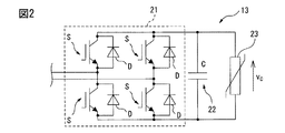
図1は、本発明の第1の実施例による回路遮断器を示す回路図であり、図2は、本発明の第1の実施例による回路遮断器における半導体電力変換器を説明する回路図である。以降、異なる図面において同じ参照符号が付されたものは同じ機能を有する構成要素であることを意味するものとする。本発明の第1の実施例による回路遮断器1は、第1のインダクタ11と、機械的遮断器12と、半導体電力変換器13と、第2のインダクタ14と、を備える。本発明の第1の実施例による回路遮断器1は、適用される直流給電システムに対して半導体電力変換器13が並列になるよう設置されるものであり、第1のインダクタ11が電源側になり、かつ機械的遮断器12が負荷側になるよう、直流給電システム上に設置される。
FIG. 1 is a circuit diagram showing a circuit breaker according to the first embodiment of the present invention, and FIG. 2 is a circuit diagram illustrating a semiconductor power converter in the circuit breaker according to the first embodiment of the present invention. is there. Hereinafter, those having the same reference numerals in different drawings mean that they are components having the same function. The
第1のインダクタ11は、一端に第1の外部接続端子T1を有する。第1の外部接続端子T1には電源側の回路が接続される。The
機械的遮断器12は、第1のインダクタ11に対して直列に接続され、第1のインダクタ11が接続される側とは反対側に第2の外部接続端子T2を有する。第2の外部接続端子T2には負荷側の回路が接続される。機械的遮断器12は、固定接触子とこの固定接触子に接触する閉路位置と固定接触子から分離される開路位置との間を移動可能な可動接触子とを有し、指令に応じて可動接触子が固定接触子から分離して開極し、電流路を遮断する。機械的遮断器12の例としては、真空遮断器、ガス遮断器もしくは空気吹付遮断器などがある。The
半導体電力変換器13は、第1のインダクタ11と機械的遮断器12とを接続する配線から分岐した配線上に、単独でもしくは複数個が互いにカスケード接続された状態で設けられる。なお、本明細書では、半導体電力変換器13が1個の場合は第2のインダクタ14が接続される側を「第1の直流側」と称し、複数個の半導体電力変換器13が互いにカスケード接続される場合は当該半導体電力変換器13とは異なる他の半導体電力変換器13が接続される側を同じく「第1の直流側」と称する。また、「第1の直流側」とは反対側の直流側を、「第2の直流側」と称する。一例として、図1では、複数個(N個、ただしNは2以上の整数)の半導体電力変換器13が第1の直流側にて互いにカスケード接続された場合を示している。カスケード接続する半導体電力変換器13の個数を適宜調整するだけで回路遮断器1の高耐圧化を容易に実現できる。
The
半導体電力変換器13は、DCDCコンバータ21と、エネルギー蓄積部22と、非線形抵抗23と、を有し、DCDCコンバータ21の内部に設けられた半導体スイッチを指令に応じてスイッチング動作させることにより所定の直流電流を出力する。
The
半導体電力変換器13内のDCDCコンバータ21は、いわゆる4象限DCDCコンバータとして構成される。すなわち、DCDCコンバータ21は、半導体スイッチSのスイッチング動作により、第1の直流側および第2の直流側のうち一方から入力された直流電流を所望の大きさおよび極性の直流電流に変換してもう一方に出力するものであり、直流電流の入出力方向は、第1の直流側と第2の直流側との間で双方向に切換え可能である。半導体電力変換器13内のDCDCコンバータ21を4象限DCDCコンバータとして構成することにより、直流電流の振幅および極性に関わりなく電流路を遮断することができる。半導体スイッチは、オン時に一方向に電流を通す半導体スイッチング素子Sと、この半導体スイッチング素子Sに逆並列に接続された帰環ダイオードDとで構成される。半導体スイッチング素子Sの例としては、IGBT、サイリスタ、GTO(Gate Turn−OFF thyristor:ゲートターンオフサイリスタ)、トランジスタなどがあるが、スイッチング素子の種類自体は本発明を限定するものではなく、その他の半導体素子であってもよい。
The
半導体電力変換器13内のエネルギー蓄積部22は、DCDCコンバータ21の第2の直流側に並列に接続される。エネルギー蓄積部22の例としては、直流コンデンサがある。直流コンデンサの場合、回路遮断器1を動作させる際にはDCDCコンバータ21を動作させて初期充電しておく。
The
半導体電力変換器13内の非線形抵抗23は、エネルギー蓄積部22に並列に接続され、エネルギー蓄積部22に印加された直流電圧が、予め設定された電圧(以下、「動作電圧」と称する。)以下の場合は所定の抵抗値を示し、それ以外の場合は所定の抵抗値よりも低い抵抗値を示す素子である。非線形抵抗23の例としては、MOV(Metal Oxide Variable Resistor)(「バリスタ」あるいは「アレスタ」とも称する)がある。非線形抵抗23の動作電圧は、使用するパワーデバイスの電圧定格に制限される。例えば、3.3[kV]耐圧のパワーデバイスを使用する場合、非線形抵抗23の動作電圧VRは3.3[kV]以下に設定する必要がある。The
直流コンデンサ22と非線形抵抗23とは並列に接続されているので、第1のインダクタ11および第2のインダクタ14に蓄積されたエネルギーによって直流コンデンサ22が充電される際には、直流コンデンサ22の充電電圧が徐々に上昇して非線形抵抗23の動作電圧に達すると、その後は直流コンデンサ22の充電電圧は非線形抵抗23の動作電圧にてクランプされ、第1のインダクタ11および第2のインダクタ14に蓄積されたエネルギーは非線形抵抗23にて消費される。なお、エネルギー蓄積部22および非線形抵抗23については、上述のような直流コンデンサ22の充電および非線形抵抗23による消費の一連の動作を行うものであれば他の素子で実現してもよく、例えば、2次電池あるいは電気二重層キャパシタなどに置き換えてもよい。
Since the
第2のインダクタ14は、本発明の第1の実施例では、半導体電力変換器13に対して直列に接続される。複数個の半導体電力変換器13が互いにカスケード接続される場合は、第2のインダクタ14は、互いにカスケード接続された複数個の半導体電力変換器13のうちのいずれかの半導体電力変換器に直列に接続される。図3A〜図3Cは、本発明の第1の実施例による回路遮断器における第2のインダクタの配置例を説明する回路図である。例えば、図3Aおよび図3Bに示すように、第2のインダクタ14は、カスケード接続の両端に位置する半導体電力変換器13のうちのいずれかの半導体電力変換器13の、当該半導体電力変換器13が接続されていない側に設置される。また例えば、図3Cに示すように、第2のインダクタ14は、互いに隣接した半導体電力変換器13の間に設置される。
In the first embodiment of the present invention, the
なお、半導体電力変換器13が1個の場合は、第2のインダクタ14は単に当該半導体電力変換器13に直列に接続される。
When there is one
複数個の半導体電力変換器13がカスケード接続される場合および半導体電力変換器13が1個の場合いずれの場合であっても、第2のインダクタ14は、互いにカスケード接続された複数個の半導体電力変換器13と同一の配線上のいずれかの位置に設けられることになる。本発明の第1の実施例では、半導体電力変換器13および第2のインダクタ14が同一配線上に位置してなるユニットは、第1のインダクタ11と機械的遮断器12との接続点Aに接続される。
Regardless of whether a plurality of
本発明の第1の実施例では、上述のように第1のインダクタ11、機械的遮断器12、半導体電力変換器13および第2のインダクタ14を結線することにより、半導体電力変換器13および第2のインダクタ14が同一配線上に位置してなるユニットの両側の2つの端子のうち、接続点Aが接続される側とは反対側の端子が、グランド端子G1およびG2となる。In the first embodiment of the present invention, the
なお、本実施例では、回路遮断器1が直流遮断器として動作する場合について説明したが、回路遮断器1は交流遮断器としても動作可能であり、この場合は、半導体電力変換器13および第2のインダクタ14が同一配線上に位置してなるユニットの両側の2つの端子のうち、接続点Aが接続される側とは反対側の端子は、第1の外部接続端子T1および第2の外部接続端子T2の極性とは反対の極性の端子G1およびG2とする。また、回路遮断器1が交流遮断器として動作する場合、半導体電力変換器13内のDCDCコンバータ21は、DCACコンバータ(直流交流変換器)として動作する。この場合、DCACコンバータの直流側は上述の「第2の直流側」に相当し、交流側は上述の「第1の直流側」に相当する。In this embodiment, the case where the
図1に示す例では、第1の外部接続端子T1およびグランド端子G1からなる側を電源側とし、第2の外部接続端子T2およびグランド端子G2からなる側を負荷側としている。したがって、第1のインダクタ11は事故電流制限用インダクタとして機能し、第2のインダクタ14は電流制御用インダクタとして機能する。In the example shown in FIG. 1, the side consisting of the first external connection terminal T 1 and the ground terminal G 1 is the power supply side, and the side consisting of the second external connection terminal T 2 and the ground terminal G 2 is the load side. Therefore, the
これ以降、電源側直流電圧をVdc、負荷電圧をvL、機械的遮断器12の両端に現れる電圧をvCB、半導体電力変換器13のカスケード接続される側の半導体電力変換器13の合計電圧をvHBで表す。また、各半導体電力変換器13に並列に接続された直流コンデンサの電圧をvC1、・・・、vCNで表す(ただし、Nは自然数)。また、第1の外部接続端子T1から接続点Aに流れる電流を電源電流iSとし、接続点Aから第2の外部接続端子T2に流れる電流を負荷電流iLとし、接続点Aから半導体電力変換器13へ流れる電流を変換器電流iHBとする。なお、図中の電圧および電流については、それぞれ矢印の向きを正としている。After that, the DC voltage on the power supply side is V dc , the load voltage is v L , the voltage appearing across the
図4は、本発明の第1の実施例による回路遮断器における制御系を説明するブロック図である。回路遮断器1は、その制御系として、過電流検出部31および制御部32を有する。
FIG. 4 is a block diagram illustrating a control system in the circuit breaker according to the first embodiment of the present invention. The
過電流検知部31は、第2の外部接続端子T2に接続された負荷側の外部配線上において過電流が発生したか否かを検知する。過電流発生の検知は公知の方法で実現すればよい。例えば、地絡や短絡などの事故が発生すると電源電流iSが増加するので、電流検出器(図示せず)を用いて電源電流iSを常時監視し、電源電流iSが定格電流より所定の値だけ大きくなった場合に「過電流発生」と判定する。過電流発生の判断に用いられる基準電流値は、例えば定格電流120%に設定するなど、必要に応じて適宜設定すればよい。The
制御部32は、機械的遮断器12に対する開極動作および半導体電力変換器13の電力変換動作を制御する。すなわち、制御部32は、過電流検知部31が過電流を検知したとき、機械的遮断器12に対して開極動作の開始を指令する開極指令を出力する第1の指令手段41と、開極指令が出力されてから機械的遮断器12の開極動作が完了するまでの間に機械的遮断器12に流れる電流をゼロに収束させる直流電流を、半導体電力変換器13に出力させる電力変換指令を出力する第2の指令手段42と、機械的遮断器12の開極動作が完了した時に、半導体電力変換器13内の半導体スイッチSをオフする指令を出力する第3の指令手段43と、を有する。
The
第1の指令手段41、第2の指令手段42および第3の指令手段43は、例えばソフトウェアプログラム形式で構築されてもよく、あるいは各種電子回路とソフトウェアプログラムとの組み合わせで構築されてもよい。例えばこれらの手段をソフトウェアプログラム形式で構築する場合は、制御部32内の演算処理装置はこのソフトウェアプログラムに従って動作することで上述の各手段の機能が実現される。
The first command means 41, the second command means 42, and the third command means 43 may be constructed, for example, in the form of a software program, or may be constructed by combining various electronic circuits and a software program. For example, when these means are constructed in the form of a software program, the functions of the above-mentioned means are realized by operating the arithmetic processing unit in the
図5は、本発明の第1の実施例による回路遮断器の動作フローを示すフローチャートである。また、図6A〜図6Dは、本発明の第1の実施例による回路遮断器の動作を説明する等価回路を示す図である。ここでは一例として、時刻t0で負荷側に地絡もしくは短絡の事故が発生して過電流が発生した場合を考える。FIG. 5 is a flowchart showing an operation flow of the circuit breaker according to the first embodiment of the present invention. 6A to 6D are diagrams showing an equivalent circuit for explaining the operation of the circuit breaker according to the first embodiment of the present invention. Here, as an example, consider a case where an accident of a ground fault or a short circuit occurs on the load side at time t 0 and an overcurrent occurs.
回路遮断器1は、負荷側に過電流が発生していないとき、正常動作を行う(ステップS101)。すなわち正常時では機械的遮断器12はオンされて電源側から負荷側に電力が供給される。このとき、半導体電力変換器13内の各ダイオードDが機能することにより、半導体電力変換器13そのものはダイオードとして動作し、変換器電流iHBはゼロとなる。したがって、正常時の回路遮断器1の定常損失はゼロである。The
また、電源側直流電圧Vdcと半導体電力変換器13内の直流コンデンサ電圧vC(=vC1=vCN)は次式の関係を満足する必要がある。Nは半導体電力変換器13の個数(換言すれば直流コンデンサの個数)を示す。Further, the DC voltage V dc on the power supply side and the DC capacitor voltage v C (= v C1 = v CN ) in the

図6Aに示すように、正常時においては、キルヒホッフの電流則より、負荷電流iLと電源電流iSとは等しく、すなわち「iL=iS」である。また、第1のインダクタL1における電圧降下は、正常時ではゼロとなるため、負荷電圧vLと電源側直流電圧Vdcとは等しく、すなわち「vL=Vdc」である。As shown in FIG. 6A, under normal conditions, according to Kirchhoff's current law, the load current i L and the power supply current i S are equal, that is, “i L = i S ”. Further, since the voltage drop in the first inductor L 1 is zero in the normal state, the load voltage v L and the power supply side DC voltage V dc are equal, that is, “v L = V dc ”.
ステップS102において、過電流検知部31は、第2の外部接続端子T2に接続された負荷側の外部配線上において過電流が発生したか否かを検知する。過電流検知部31が過電流を検知しなかったときはステップS101に戻り正常動作を継続する。過電流検知部31が過電流を検知したときはステップS103へ進む。In step S102, the
例えば時刻t1で過電流検知部31が過電流の発生を検知したとすると、負荷側の事故発生直後である時刻t0から時刻t1までの期間における回路遮断器10の等価回路は図6Bのように表される。機械的遮断器12における電圧降下を無視すると、式2に示される回路方程式が成立する。For example, when the
式2から、電源電流iSおよび負荷電流iLは式3のように表される。ただし、式3において、I0は時刻t0における電流を表す。From
式3から分かるように、電源電流iSおよび負荷電流iLは「Vdc/L1」の傾きで1次関数的に増加する。すなわち、第1のインダクタ11のインダクタンスL1を増加させれば事故時の電流増加率を抑制できる。短絡や地絡事故が発生すると電源電流iSは増加するため、過電流検知部31は、電流検出器(図示せず)を用いて電源電流iSを常時監視し、電源電流iSが定格電流より所定の値だけ大きくなった場合(例えば定格電流120%)に「過電流発生」と判定する。事故発生から事故判断に要する時間「t1−t0」は電源側直流電圧Vdc、第1のインダクタのインダクタンスL1、負荷、基準電流値などに依存する。As can be seen from Equation 3, the power supply current i S and the load current i L increase linearly with the slope of “V dc / L 1 ”. That is, if the inductance L 1 of the
ステップS102において過電流検知部31が過電流を検知したとき、ステップS103において、制御部32の第1の指令手段は、機械的遮断器12に対して開極動作の開始を指令する開極指令を出力する。
When the
機械的遮断器12に開極指令を与えても機械的遮断器12は直ちに開極動作を完了するのではなく、機械的遮断器12の機械的構造に起因する遅れ時間が発生し、実際には少し遅れて開極動作を完了する。例えば、直流電圧が数10[kV]クラスでは1[ms]以下、数100[kV]クラスでは2[ms]程度の遅れ時間が発生する。機械的遮断器12はゼロ電流時のみ電流路を遮断することが可能であるため、機械的遮断器12を流れる負荷電流iLをゼロにする必要がある。そこで、ステップS104において、制御部32の第2の指令手段42は、開極指令が出力されてから機械的遮断器12の開極動作が完了するまでの間に機械的遮断器12に流れる電流をゼロに収束させる直流電流を、半導体電力変換器13に出力させる電力変換指令を出力する。半導体電力変換器13内のDCDCコンバータ21内にある半導体スイッチの半導体スイッチング素子Sは受信した電力変換指令に基づいてPWMスイッチング動作を行う。これにより、図6Cに示すように、半導体電力変換器13はvHBを出力する制御電圧源として動作することと等価になる。図6Cにおいて、式4のような回路方程式が成立する。Even if an opening command is given to the
本発明の第1の実施例では、制御電圧源については、一例としてPI制御にて実現し、vHBを式5で与える。式5において、Kpは比例ゲインを表し、KIは積分ゲインを表し、i* HBは変換器電流の指令値を表す。なお、本実施例ではPI制御を適用したが、PI制御以外の電流制御を適用してもよい。In the first embodiment of the present invention, the control voltage source is realized by PI control as an example, and v HB is given by
式5において、右辺第1項および第2項はフィードフォワード制御に相当し、右辺第3項はフィードバック制御(PI)に相当する。式5を式4に代入すると式6が得られる。
In
式6に示すように、変換器電流iHBはその指令値i* HBに対して2次遅れで応答する。このとき、変換器電流の指令値i* HBをiSに設定して変換器電流iHBを電源電流iSに一致させる制御を行えば、負荷電流iLをゼロにすることができる。負荷電流iLをゼロにするのに要する時間(すなわち、変換器電流iHBを電源電流iSに一致させるのに要する時間)は、半導体電力変換器13のキャリア周波数、等価スイッチング周波数、ディジタル制御手法に依存する。例えば低損失かつ高スイッチング周波数動作を実現可能な高圧SiC MOSFETを用いれば、負荷電流iLをゼロにするのに要する時間を1[ms]以下に実現することは十分可能である。As shown in
以上を踏まえ、式5に基づく電力変換指令の生成原理を説明すると次の通りである。図7は、本発明の第1の実施例による回路遮断器内の半導体電力変換器における変換器電流を制御するための電力変換指令を説明する制御ブロック図である。変換器電流の制御では、フィードバック制御とフィードフォワード制御を併用する。フィードバック制御に係るブロックB1では、電流検出器(図示せず)によって検出された変換器電流iHBと電流検出器(図示せず)によって検出された電源電流iSの差分に対しPI制御を適用することで偏差「iHB−iS」を抑制する。一方、フィードフォワード制御に係るブロックB2では、半導体電力変換器13の両端に現れる電圧vHBと第2のインダクタ14の両端に現れる電圧との総和vfを利用することで、電流制御性向上を実現する。vfは、直流電源側電圧Vdc、電源電流iS、および第1のインダクタ11のインダクタンスL1を用いて算出するか、あるいは電圧センサ(図示せず)を用いて直接検出することで得ればよい。ブロックB1の出力とブロックB3の出力とが加算されて各半導体電力変換器13に対する電力変換指令v* jが生成される。各半導体電力変換器13に対する電力変換指令v* jは、ブロックB4jにて直流コンデンサ電圧vCj(ただし、j=1〜N)で規格化した後、一般的なPWM変調法(三角波比較)を適用して各半導体電力変換器13内の半導体スイッチSへ与えられる。ここで、各半導体電力変換器13のPWM制御に用いられる三角波キャリアの初期位相を180°/N移相する「位相シフトPWM」を適用すれば、等価スイッチング周波数を増加できる。具体的には、キャリア周波数をfCとすると、等価スイッチング周波数は2NfCとなる。等価スイッチング周波数を高く設定することで、電流制御系の向上と電流制御インダクタとしての第2のインダクタ14のインダクタンスの低減を実現できる。Based on the above, the principle of generating the power conversion command based on
一般に、高圧用途の半導体電力変換器のスイッチング周波数は、スイッチング損失低減の観点から数100[Hz]に設定される。一方、本発明の第1の実施例による回路遮断器1内の半導体電力変換器13は事故発生時のみPWM動作を行うため、スイッチング損失の増大は問題とならない。半導体電力変換器13として例えば3.3[kV]/1500[A]のSiCパワーモジュール(SiC MOSFETとSiC SBD(Schottky Barrier Diode))を使用した場合、PWM変調には数[kHz]のキャリア周波数適用が想定され、電流制御性の向上が期待できる。同一キャリア周波数を想定した場合、半導体電力変換器13のカスケード数が多くなるような高圧用途における電流制御性が向上する。
Generally, the switching frequency of a semiconductor power converter for high voltage applications is set to several hundreds [Hz] from the viewpoint of reducing switching loss. On the other hand, since the
以上、ステップS104における電力変換指令の出力について説明したが、ステップS104における処理は、ステップS103における開極指令の出力と同時に実行されてもよい。 Although the output of the power conversion command in step S104 has been described above, the process in step S104 may be executed at the same time as the output of the open pole command in step S103.
図5に戻ると、ステップS105において、機械的遮断器12は、制御部32内の第2の指令手段42からの開極指令に応じて開極動作を開始する。上述のように機械的遮断器12はゼロ電流時のみ動作可能であるが、ステップS104における機械的遮断器12に流れる電流をゼロにする処理は、開極指令が出力されてから機械的遮断器12の開極動作が完了するまでに要する時間よりも十分短い時間に実行される。
Returning to FIG. 5, in step S105, the
機械的遮断器12の開極動作が完了したとき(ここでは時刻t2とする)、ステップS106において、制御部32内の第3の指令手段43は、半導体電力変換器13内の全ての半導体スイッチSをオフする指令を出力する。半導体電力変換器13の電力変換動作開始から機械的遮断器12の開極動作完了までに要する時間「t2−t1」は、機械的遮断器12に対して開極指令を与えてから機械的遮断器12が実際に開極動作を完了するまでの遅れ時間と等しく、その時間は例えば2[ms]である。When the opening operation of the
制御部32内の第3の指令手段43によるオフ指令を受信して半導体電力変換器13内の全ての半導体スイッチSはターンオフし、電力変換動作は終了する。これにより、図6Dに示すように、半導体電力変換器13内の各ダイオードDのみが機能することになる。このとき、第1のインダクタ11および第2のインダクタ14の蓄積エネルギーは、帰環ダイオードDを介して直流コンデンサ22および非線形抵抗23に放出される。直流コンデンサ22と非線形抵抗23とは並列に接続されているので、半導体スイッチSはターンオフ後(すなわち時刻t2以降の期間)は、第1のインダクタ11および第2のインダクタ14の蓄積エネルギーによって直流コンデンサ22が充電され、電圧vcは、徐々に上昇した後、非線形抵抗23の動作電圧VRでクランプされる。直流コンデンサ22が当該動作電圧まで充電された後は、蓄積エネルギーは非線形抵抗23にて消費される。Upon receiving the off command from the third command means 43 in the
蓄積エネルギーによって直流コンデンサ22が非線形抵抗23の動作電圧まで充電されるまでは、式7に示す回路方程式が成立する。
The circuit equation shown in Equation 7 holds until the
式7より、直流コンデンサ22の電圧vCおよび電源電流iS(=iHB)は2階定数係数線形微分方程式を解くことで算出できる。From Equation 7, the voltage v C of the
直流コンデンサ22が当該動作電圧まで充電された後は、式8に示す回路方程式が成立する。式8において、非線形抵抗23の動作電圧をVRとする。After the
式8より、電源電流iSおよび変換器電流iHBは1階定数係数線形微分方程式を解くことで算出できる。From Equation 8, the power supply current i S and the converter current i HB can be calculated by solving the first-order constant coefficient linear differential equation.
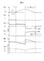
次に、本発明の第1の実施例による回路遮断器のシミュレーション結果について説明する。図8Aは本発明の第1の実施例による回路遮断器のシミュレーションに用いた回路図であって、回路遮断器にRL負荷を接続したときに回路遮断器の至近端で短絡事故が発生した場合の回路図を示す。また、図8Bは本発明の第1の実施例による回路遮断器のシミュレーションに用いた回路図であって、回路遮断器に回生負荷を接続したときに回路遮断器の至近端で短絡事故が発生した場合の回路図を示す。ただし、図8Bにおいて、回生負荷は直流電流源で模擬している。また、図9は、図8Aおよび図8Bに示すシミュレーション回路図の回路パラメータを説明する図である。シミュレーションには「PSCAD/EMTDC」を使用した。高圧用途への適用を想定し定格容量Pは7.5[MW]、定格直流電圧Vdcは15[kV]、定格電源電流ISは500[A]、定格負荷電流ILは500[A]とした。第1のインダクタ(事故時電流制限用インダクタ)のインダクタンスL1は、電流増加率Vdc/L1が1.5[kA/ms]となるよう10[mH]とした。また、3.3[kV]耐圧の半導体スイッチング素子を想定し、初期直流コンデンサ電圧は1.5[kV]、半導体電力変換器13の個数Nは10、キャリア周波数fCは2[kHz]とした。単位静電定数Hは、直流コンデンサの全静電エネルギーを変換器容量で規格化した値(単位は[s])であり、式9で表せる。Next, the simulation result of the circuit breaker according to the first embodiment of the present invention will be described. FIG. 8A is a circuit diagram used in the simulation of the circuit breaker according to the first embodiment of the present invention, in which a short-circuit accident occurred at the nearest end of the circuit breaker when the RL load was connected to the circuit breaker. The circuit diagram of the case is shown. Further, FIG. 8B is a circuit diagram used for simulating the circuit breaker according to the first embodiment of the present invention, and when a regenerative load is connected to the circuit breaker, a short-circuit accident occurs at the nearest end of the circuit breaker. The circuit diagram when it occurs is shown. However, in FIG. 8B, the regenerative load is simulated by a DC current source. Further, FIG. 9 is a diagram for explaining the circuit parameters of the simulation circuit diagrams shown in FIGS. 8A and 8B. "PSCAD / EMTDC" was used for the simulation. Rated capacity P is 7.5 assuming application to high pressure applications [MW], rated DC voltage V dc is 15 [kV], the rated source current I S is 500 [A], the rated load current I L 500 [A ]. The inductance L 1 of the first inductor (inductor for limiting the current at the time of accident) was set to 10 [mH] so that the current increase rate V dc / L 1 was 1.5 [kA / ms]. Assuming a semiconductor switching element with a withstand voltage of 3.3 [kV], the initial DC capacitor voltage is 1.5 [kV], the number N of
また、シミュレーションでは、制御遅延がゼロであるアナログ制御系を想定し、半導体スイッチング素子のデッドタイムはゼロとした。また、電流発生の判断に用いられる基準電流値は定格電流120%に設定した。また、非線形抵抗23は、動作電圧を2[kV]とし、印加される電圧が2[kV]以下の場合無限大の抵抗値を示し、2[kV]以上は抵抗値がゼロを示すものとした。また、機械的遮断器12は、インピーダンスがゼロの理想スイッチとして模擬し、開極指令受信から開極動作完了までの遅れ時間(=t2−t1)を1.5[ms]とした。In the simulation, an analog control system with zero control delay was assumed, and the dead time of the semiconductor switching element was set to zero. Further, the reference current value used for determining the current generation was set to the rated current of 120%. Further, the
図10は、本発明の第1の実施例による回路遮断器を図8Aのシミュレーション回路にて動作させた場合のシミュレーション波形を示す図である。また、図11は、図10の時間軸拡大波形を示す図である。なお、図11において、機械的遮断器12の両端に現れる電圧vCBおよび直流コンデンサ電圧については省略している。回路遮断器1にRL負荷(7.5[MW])を接続したときに時刻t0の時点で回路遮断器1の至近端で短絡事故が発生した場合を考える。FIG. 10 is a diagram showing a simulation waveform when the circuit breaker according to the first embodiment of the present invention is operated by the simulation circuit of FIG. 8A. Further, FIG. 11 is a diagram showing an enlarged time axis waveform of FIG. In FIG. 11, the voltage v CB and the DC capacitor voltage appearing at both ends of the
短絡事故が発生する時刻t0以前における半導体電力変換器13は、半導体電力変換器13内の各ダイオードDが機能することにより、半導体電力変換器13そのものはダイオードとして動作する。この場合は負荷電流iLは電源電流iSと同じ500[A]となり、キルヒホッフの電流則より変換器電流iHBは0[A]となる。したがって、直流側電源電圧Vdcと変換器電圧vHBは等しくなり、ともに15[kV]である。この間、各半導体電力変換器13内の直流コンデンサ22の電圧(Vdc/N)はそれぞれ1.5[kV]に充電される。In the
時刻t0において短絡事故が発生すると、電源電流iSと変換器電流iLは1.5[kA/ms](=Vdc/L1)の傾きで増加する。電源電流iSと負荷電流iLは、約70[μs]の期間で600[A](すなわち定格電流の120%)に到達する。式2および式4ならびに「iHB=0」の関係式より、変換器電圧vHBはゼロに減少する。When a short-circuit accident occurs at time t 0 , the power supply current i S and the converter current i L increase with a slope of 1.5 [kA / ms] (= V dc / L 1 ). The power supply current i S and the load current i L reach 600 [A] (that is, 120% of the rated current) in a period of about 70 [μs]. From
時刻t1において、機械的遮断器12に開極指令を与える。同時に、機械的遮断器12に流れる電流をゼロに収束させる直流電流を半導体電力変換器13に出力させる電力変換指令を出力する。これにより半導体電力変換器13内の半導体スイッチSは受信した電力変換指令に基づいてPWMスイッチング動作を行う。図11に示すように、電流制御適用後0.35[ms]で負荷電流iLはゼロとなり、機械的遮断器12により電流路の遮断が可能な状態となる。時刻t1直後の変換器電圧vHBは負電圧となる。図11に示すように、変換器電圧vHBは−5[kV]まで低下する。この電圧低下量は、変換器電流iHBと電源電流iSとの偏差量と制御ゲイン値とに依存する。このとき、半導体電力変換器13から電力が出力される半導体電力変換器13内の直流コンデンサ22の直流電圧vC1およびvC2は減少する。この減少量は、PWM動作開始および開極指令受信から機械的遮断器12の開極完了までの時間「t2−t1」が短いほど低減できる。本シミュレーションでは、時間「t2−t1」を1.5[ms]と設定した。At time t 1, it gives the opening command to the
時刻t2において機械的遮断器12の開極動作が完了し、同時に半導体電力変換器13内のDCDCコンバータ21内の全ての半導体スイッチの半導体スイッチング素子Sをターンオフする。直流コンデンサ22の直流電圧vC1およびvC2は、式7の回路方程式に従い、非線形抵抗23の動作電圧(2.0[kV])まで増加する。その後、式8の回路方程式に従い、電源電流iSと変換器電流iHBは一次関数的に減少する。式8より、電流変化率は式10で表される。Complete opening operation of the
式10に図9の回路定数を代入すると、電流変化率は−0.5[kA/ms]となり図10のシミュレーション結果と整合する。ただし、VRは非線形抵抗23の動作電圧である2[kV]とした。Substituting the circuit constant of FIG. 9 into
一方、機械的遮断器12の両端に現れる電圧vCBは、図1および式10より式11のようになる。On the other hand, the voltage v CB appearing at both ends of the
式11に図9の回路定数と非線形抵抗23の動作線圧VR=2[kV]を代入すると機械的遮断器12の両端に現れる電圧vCBは20[kV]となり、図10のシミュレーション結果と整合する。式11より、「NVR−Vdc」を零に近づけることで機械的遮断器12の両端に現れる電圧vCBを低減できるが、電流減少率が低下するため非線形抵抗23の消費電力は増加する。時刻t3以降は電源電流iSはゼロとなるため、式11より「vCB=Vdc=15[kV]」となる。本シミュレーション結果によれば、短絡事故発生から電流遮断完了までの所要時間「t3−t0」は7.7[ms]であり、回路遮断器1により高速遮断を実現できることがわかる。Substituting the circuit constant of FIG. 9 and the operating linear pressure V R = 2 [kV] of the
図12は、本発明の第1の実施例による回路遮断器を図8Bのシミュレーション回路にて動作させた場合のシミュレーション波形を示す図である。回路遮断器1に回生負荷(7.5[MW])を接続したときに時刻t0の時点で回路遮断器1の至近端で短絡事故が発生した場合を考える。FIG. 12 is a diagram showing a simulation waveform when the circuit breaker according to the first embodiment of the present invention is operated by the simulation circuit of FIG. 8B. Consider a case where a short-circuit accident occurs at the nearest end of the
本シミュレーションでは回生負荷を想定しているため、短絡事故が発生する時刻t0以前の正常時は電源電流iSおよび負荷電流iLはともに−500[A]となる。時刻t0での短絡事故発生から事故検知までの所要時間「t1−t0」は680[μs]となる。各部波形は、図10と同様となる。本シミュレーション結果によれば、短絡事故発生から電流遮断完了までの所要時間「t3−t0」は8.3[ms]であり、回路遮断器1により高速遮断を実現できることがわかる。Since a regenerative load is assumed in this simulation, the power supply current i S and the load current i L are both −500 [A] in the normal state before the time t 0 when the short circuit accident occurs. The time required from the occurrence of the short-circuit accident at time t 0 to the detection of the accident “t 1 − t 0 ” is 680 [μs]. The waveform of each part is the same as in FIG. According to the results of this simulation, the time required from the occurrence of the short circuit accident to the completion of the current cutoff "t 3- t 0 " is 8.3 [ms], and it can be seen that the
以上説明した本発明の第1の実施例では、回路遮断器1は第1のインダクタ11が電源側になり、かつ機械的遮断器12が負荷側になるよう、直流給電システム上に配置されることを想定したものであるが、この変形例として、回路遮断器1の接続を電源側と負荷側とで入れ替えてもよい。図13は、本発明の第1の実施例による回路遮断器の変形例を示す回路図である。
In the first embodiment of the present invention described above, the
図13に示すように、本発明の第1の実施例の変形例では、回路遮断器1は第1のインダクタ11が負荷側になり、かつ機械的遮断器12が電源側になるよう、直流給電システム上に配置されることを想定したものである。すなわち、第1のインダクタ11の第1の外部接続端子T1に負荷側の回路が接続され、機械的遮断器12の第2の外部接続端子T2に電源側の回路が接続される。回路遮断器1に対する電源側と負荷側との接続関係が反対になること以外は、本変形例は図1〜図7を参照して説明した第1の実施例と同様である。すなわち、本変形例における第1のインダクタ11、機械的遮断器12、半導体電力変換器13、および第2のインダクタ14の各構成、ならびに制御系は、第1の実施例と同様である。As shown in FIG. 13, in the modified example of the first embodiment of the present invention, the
本発明の第1の実施例の変形例における回路遮断器のシミュレーション結果について説明する。シミュレーション回路として、図8Aおよび図8Bにおいて示した回路遮断器1を変形例における回路遮断器1に置き換えたものを用いた。シミュレーションに用いた回路パラメータのうち、非線形抵抗23については、DCDCコンバータ21の過変調を防止するため、動作電圧を2[kV]とし、印加される電圧が2[kV]以下の場合無限大の抵抗値を示し、2[kV]以上は抵抗値がゼロを示すものとした。これ以外の回路パラメータは、上述の第1の実施例のシミュレーションに用いた図9に示したものを用いた。また、事故発生の時刻や電流制御系適用の時刻等も上述の第1の実施例と同様とした。
The simulation result of the circuit breaker in the modified example of the 1st Example of this invention will be described. As the simulation circuit, the
図14は、本発明の第1の実施例の変形例による回路遮断器を図8Aのシミュレーション回路にて動作させた場合のシミュレーション波形を示す図である。回路遮断器1にRL負荷(7.5[MW])を接続したときに時刻t0の時点で回路遮断器1の至近端で短絡事故が発生した場合を考える。FIG. 14 is a diagram showing a simulation waveform when a circuit breaker according to a modified example of the first embodiment of the present invention is operated by the simulation circuit of FIG. 8A. Consider a case where a short-circuit accident occurs at the nearest end of the
上述の通り、半導体電力変換器13内のDCDCコンバータ21の過変調を防止するため、短絡事故が発生する時刻t0以前の正常時も直流コンデンサ22の電圧vCを2[kV]に制御する必要がある。具体的には、各DCDCコンバータ21にPWM制御を適用することで、正常時における半導体電力変換器13の動作モードであるダイオード動作時の1.5[kV]から2[kV]に昇圧する。図14に示すように、電源電流iSおよび変換器電流vHBにはスイッチングリプル成分が重畳する。半導体電力変換器13が消費する電力は、直流コンデンサ22に対する電圧一定制御の実現に必要な電力分に相当し、負荷電力と比較して十分に小さい。したがって、PWM制御に起因する損失は無視できる。事故発生直後(時刻t0〜時刻t1)においても各DCDCコンバータ21はPWM動作を行い、VC=2[kV]を実現する。As described above, in order to prevent overmodulation of the
時刻t1において、機械的遮断器12に開極指令を与える。同時に、機械的遮断器12に流れる電流をゼロに収束させる直流電流を半導体電力変換器13に出力させる電力変換指令を出力する。具体的には、負荷側電流iLと変換器電流−iHBとの間の偏差がゼロになるように制御することで、電源電流iSをゼロにする。これにより、機械的遮断器12を遮断動作させることができる。At time t 1, it gives the opening command to the
第1の実施例のシミュレーション結果を示す図10と本変形例のシミュレーション結果を示す図14とを比較すると、時刻t1〜t2における変換器電力pHBの変動幅は、本変形例による回路遮断器1の方が大きい。これは、第1の実施例による回路遮断器1における変換器電圧vHBがゼロ近傍の値となるのに対して、本変形例による回路遮断器1における変換器電圧vHBは電源電圧Vdc(15[kV])近傍の値となることに起因する。その結果、本変形例による回路遮断器1における直流コンデンサ電圧の減少幅は、第1の実施例による回路遮断器1の場合と比較し大きい。時刻t2において機械的遮断器12の開極動作が完了し、同時に全半導体スイッチをターンオフする。第1の実施例のシミュレーション結果を示す図10と本変形例のシミュレーション結果を示す図14とを比較すると、iL(=−iHB)がゼロに収束するまでの時間は、第1の実施例による回路遮断器1の方が短い。本変形例による回路遮断器1における電流変化率は、式12で表せる。Comparing FIG. 10 showing the simulation result of the first embodiment with FIG. 14 showing the simulation result of the present modification, the fluctuation range of the converter power p HB at times t 1 to t 2 is the circuit according to the present modification. The
式12に図9に示す回路定数とVC=2[kV]を代入すると、電流変化率は−2[kA/ms]となり、1.5[ms]で−3[kA]となるシミュレーション結果と整合する。Substituting circuit constant and V C = 2 shown in FIG. 9 [kV] in
一方、機械的遮断器12の開極動作の完了後の変換器電圧vHBは、図13と式12より式13のように表せる。On the other hand, the converter voltage v HB after the completion of the opening operation of the
式13にN=10、VR=2[kV]を代入すると変換器電圧vHB=−20[kV]となりシミュレーション結果と一致する。このとき、機械的遮断器12の両端に現れる電圧vCBは、図13より式14のように表せる。ここで、第2のインダクタ14の両端の電圧降下はゼロとした。Substituting N = 10 and V R = 2 [kV] into
式14にVdc=15[kV]、vHB=−20[kV]を代入するとvCB=35kVとなり、シミュレーション結果と一致する。時刻t3以降は変換器電圧vHBはゼロとなるため、式14より機械的遮断器12の両端に現れる電圧vCBは15[kV]となる。本シミュレーション結果によれば、短絡事故発生から電流遮断完了までの所要時間「t3−t0」は3[ms]であり、第1の実施例による回路遮断器1と比較してさらに高速に遮断ができることがわかる。Substituting V dc = 15 [kV] and v HB = -20 [kV] into
図15は、本発明の第1の実施例の変形例による回路遮断器を図8Bのシミュレーション回路にて動作させた場合のシミュレーション波形を示す図である。回路遮断器1に回生負荷(7.5[MW])を接続したときに時刻t0の時点で回路遮断器1の至近端で短絡事故が発生した場合を考える。図15に示すように、各部波形は、RL負荷時と同様となる。本シミュレーション結果によれば、短絡事故発生から電流遮断完了までの所要時間「t3−t0」は3.7[ms]であり、高速遮断を実現できていることがわかる。FIG. 15 is a diagram showing a simulation waveform when a circuit breaker according to a modified example of the first embodiment of the present invention is operated by the simulation circuit of FIG. 8B. Consider a case where a short-circuit accident occurs at the nearest end of the
次に、本発明の第2の実施例について説明する。図16は、本発明の第2の実施例による回路遮断器における半導体電力変換器を説明する回路図である。上述の第1の実施例による回路遮断器1は、適用される直流給電システムに対して半導体電力変換器13が並列になるよう設置されたが、本発明の第2の実施例による回路遮断器2は、直流給電システムに対して半導体電力変換器13が直列になるよう設置される。本発明の第2の実施例による回路遮断器2は、第1の実施例同様、第1のインダクタ11と、機械的遮断器12と、半導体電力変換器13と、第2のインダクタ14と、を備える。
Next, a second embodiment of the present invention will be described. FIG. 16 is a circuit diagram illustrating a semiconductor power converter in a circuit breaker according to a second embodiment of the present invention. The
第1のインダクタ11は、一端に第1の外部接続端子T1を有する。第1の外部接続端子T1には電源側の回路が接続される。第1のインダクタ11の構成については第1の実施例において説明したものと同様である。The
機械的遮断器12は、第1のインダクタ11に対して直列に接続され、第1のインダクタ11が接続される側とは反対側に第2の外部接続端子T2を有する。第2の外部接続端子T2には負荷側の回路が接続される。機械的遮断器12の構成については第1の実施例において説明したものと同様である。The
半導体電力変換器13は、第1のインダクタ11と機械的遮断器12とを接続する配線から分岐した配線上に、単独でもしくは複数個が互いにカスケード接続された状態で設けられる。第1の実施例同様、半導体電力変換器13が1個の場合は第2のインダクタ14が接続される側を「第1の直流側」と称し、また、複数個の半導体電力変換器13が互いにカスケード接続される場合は当該半導体電力変換器13とは異なる他の半導体電力変換器13が接続される側を同じく「第1の直流側」と称する。また、「第1の直流側」とは反対側の直流側を、「第2の直流側」と称する。一例として、図16では、複数個(N個、ただしNは2以上の整数)の半導体電力変換器13が第1の直流側にて互いにカスケード接続された場合を示している。半導体電力変換器13の構成については第1の実施例において説明したものと同様である。ただし、半導体電力変換器13内のエネルギー蓄積部22を直流コンデンサとした場合は、第1の実施例の場合とは異なり、初期充電回路(図示せず)を別途設ける必要がある。
The
第2のインダクタ14は、本発明の第2の実施例では、半導体電力変換器13に対して直列に接続される。第1の実施例の場合と同様、複数個の半導体電力変換器13が互いにカスケード接続される場合は、第2のインダクタ14は、図3A〜図3Cに示すように互いにカスケード接続された複数個の半導体電力変換器13のうちのいずれかの半導体電力変換器に直列に接続され、半導体電力変換器13が1個の場合は、第2のインダクタ14は単に当該半導体電力変換器13に直列に接続される。
In the second embodiment of the present invention, the
複数個の半導体電力変換器13がカスケード接続される場合および半導体電力変換器13が1個の場合いずれの場合であっても、第2のインダクタ14は、互いにカスケード接続された複数個の半導体電力変換器13と同一の配線上のいずれかの位置に設けられる。そして、本発明の第2の実施例では、半導体電力変換器13および第2のインダクタ14が同一配線上に位置してなるユニットは、機械的遮断器12に対して並列に接続される。
Regardless of whether a plurality of
本発明の第2の実施例では、第1の外部接続端子T1および第2の外部接続端子T2それぞれに対応してグランド端子G1およびG2が設けられる。なお、回路遮断器2は直流遮断器するほかに交流遮断器としても動作可能であり、この場合は、端子G1およびG2は第1の外部接続端子T1および第2の外部接続端子T2の極性とは反対の極性を有する端子となる。In the second embodiment of the present invention, ground terminals G 1 and G 2 are provided corresponding to the first external connection terminal T 1 and the second external connection terminal T 2, respectively. The
また、回路遮断器1が交流遮断器として動作する場合、半導体電力変換器13内のDCDCコンバータ21は、DCACコンバータ(直流交流変換器)として動作する。DCACコンバータの直流側は上述の「第2の直流側」に相当し、交流側は上述の「第1の直流側」に相当する。
When the
図16に示す例では、第1の外部接続端子T1およびグランド端子G1からなる側を電源側とし、第2の外部接続端子T2およびグランド端子G2からなる側を負荷側としている。したがって、第1のインダクタ11は事故電流制限用インダクタとして機能し、第2のインダクタ14は電流制御用インダクタとして機能する。In the example shown in FIG. 16, the side consisting of the first external connection terminal T 1 and the ground terminal G 1 is the power supply side, and the side consisting of the second external connection terminal T 2 and the ground terminal G 2 is the load side. Therefore, the
ここで、電源側直流電圧をVdc、負荷電圧をvL、機械的遮断器12の両端に現れる電圧をvCB、半導体電力変換器13のカスケード接続される側の半導体電力変換器13の合計電圧をvHBで表す。また、各半導体電力変換器13に並列に接続された直流コンデンサの電圧をvC1、・・・、vCNで表す。また、第1の外部接続端子T1から第1のインダクタ11に流れる電流を電源電流iSとし、接続点Aから第2の外部接続端子T2に流れる電流を負荷電流iLとし、接続点Aから半導体電力変換器13へ流れる電流を変換器電流iHBとする。なお、図中の電圧および電流については、それぞれ矢印の向きを正としている。Here, the DC voltage on the power supply side is V dc , the load voltage is v L , the voltage appearing at both ends of the
本発明の第2の実施例による回路遮断器2の動作も、図5を参照して説明した第1の実施例による回路遮断器1の動作フローと同様に動作する。すなわち、時刻t0で負荷側に地絡もしくは短絡の事故が発生して過電流が発生し、時刻t1において機械的遮断器12に開極指令を与えると同時に各半導体電力変換器13内のDCDCコンバータ21の電力変換動作を開始させる。また、時刻t2において機械的遮断器12の開極動作が完了すると同時に全半導体スイッチSをターンオフし、時刻t3において電源電流iSと変換器電流iHBが零となり電流遮断が完了する。より詳しくは次の通りである。The operation of the
短絡事故が発生する時刻t0以前の正常時の回路遮断器2の動作は、第1の実施例による回路遮断器1の動作と同じである。すなわち正常時では機械的遮断器12はオンされて電源側から負荷側に電力が供給される。このとき、半導体電力変換器13内の各ダイオードDが機能することにより、半導体電力変換器13そのものはダイオードとして動作し、変換器電流iHBはゼロとなり、電源電流isと負荷電流iLは同一となる。また、第1の実施例と異なり、電源側直流電圧Vdcと半導体電力変換器13内の直流コンデンサ電圧vC(=vC1=vCN)は式1の関係を満足する必要はない。The operation of the
時刻t1で過電流検知部31が過電流の発生を検知した直後の回路遮断器2の動作も、第1の実施例による回路遮断器1の動作と同じである。電源電流iSおよび負荷電流iLは式3に示すように「Vdc/L1」の傾きで1次関数的に増加する。The operation of the
時刻t1から時刻t2までの間に実行される回路遮断器2内の半導体電力変換器13の動作も、第1の実施例の場合と同じである。ただし、半導体電力変換器における変換器電流のための制御系は、第1の実施例の場合と異なる。これについては後述する。The operation of the
時刻t2で機械的遮断器12の開極動作が完了したときの回路遮断器2の動作も、第1の実施例による回路遮断器1の動作と同じである。すなわち半導体電力変換器13内のDCDCコンバータ21内の全ての半導体スイッチング素子Sをオフすることで、第1のインダクタ11および第2のインダクタ14の蓄積エネルギーは、帰環ダイオードDを介して直流コンデンサ22および非線形抵抗23に放出される。この期間において成立する電圧方程式や電流の関係式は、第1の実施例の場合と同一である。The operation of the
ここで、半導体電力変換器における変換器電流のための制御系について説明する。図17は、本発明の第2の実施例による回路遮断器内の半導体電力変換器における変換器電流を制御するための電力変換指令を説明する制御ブロック図である。第2の実施例では、図7を参照して説明した第1の実施例と同様、変換器電流を制御するための電力変換指令の生成原理を適用することで、変換器電流iHBを電源電流iSに一致させる制御を行い、負荷電流iLがゼロになるようにする。ただし、図7に示した第1の実施例におけるフィードフォワード制御に関わるブロックB2は使用せず、図17に示すようにフィードバック制御に係わるブロックB1のみ使用する。フィードバック制御に係るブロックB1では、変換器電流iHBと電源電流iSの差分に対しPI制御を適用することで偏差「iHB−iS」を抑制する。この代替例として、変換器電流iHBと電源電流iSの差分に対しP制御を適用することで偏差「iHB−iS」を抑制してもよい。ブロックB1にて各半導体電力変換器13に対する電力変換指令v* j(ただし、j=1〜N)が生成される。各半導体電力変換器13に対する電力変換指令v* jは、ブロックB4jにて直流コンデンサ電圧vCj(ただし、j=1〜N)で規格化した後、一般的なPWM変調法(三角波比較)を適用して各半導体電力変換器13内の半導体スイッチSへ与えられる。第1の実施例の場合同様、各半導体電力変換器13のPWM制御に用いられる三角波キャリアの初期位相を180°/N移相する「位相シフトPWM」を適用すれば、等価スイッチング周波数を増加できる。具体的には、キャリア周波数をfCとすると、等価スイッチング周波数は2NfCとなる。等価スイッチング周波数を高く設定することで、電流制御系の向上と電流制御インダクタとしての第2のインダクタ14のインダクタンスの低減を実現できる。Here, the control system for the converter current in the semiconductor power converter will be described. FIG. 17 is a control block diagram illustrating a power conversion command for controlling a converter current in a semiconductor power converter in a circuit breaker according to a second embodiment of the present invention. In the second embodiment, as in the first embodiment described with reference to FIG. 7, the converter current i HB is powered by applying the power conversion command generation principle for controlling the converter current. Control to match the current i S so that the load current i L becomes zero. However, the block B2 related to the feedforward control in the first embodiment shown in FIG. 7 is not used, and only the block B1 related to the feedback control is used as shown in FIG. In the block B1 related to the feedback control, the deviation “i HB − i S ” is suppressed by applying the PI control to the difference between the converter current i HB and the power supply current i S. As an alternative example, the deviation "i HB- i S " may be suppressed by applying P control to the difference between the converter current i HB and the power supply current i S. In block B1, a power conversion command v * j (where j = 1 to N) is generated for each
ここで、変換器電流を制御するために設けられる電流検出器についてより詳細に説明する。図17に示すように、電源電流iSを検出するために電流検出器33が設けられ、変換器電流iHBを検出するために電流検出器34が設けられる。各電流検出器33および34の電流検出範囲の最大値は、事故遮断電流と等しい。このため、各電流検出器33および34の検出誤差が図17を参照して説明した電流制御系に悪影響を及ぼす可能性がある。一般に、事故遮断電流は正常時の電流の5〜10倍に設定される。例えば正常時の電源電流iSを500[A]とし、事故遮断電流をその10倍と仮定すると、各電流検出器33および34は、最大5000[A]の電流を検出できなければならない。一方で、電流検出器には必ず検出誤差が存在する。例えば各電流検出器33および34の検出誤差を1%とした場合、各電流検出器33および34には50[A]もの誤差が発生することになり、図17を参照して説明した電流制御系に悪影響を及ぼす可能性がある。そこで、電流検出器を次に説明する第1および第2の変形例のように構成してもよい。Here, the current detector provided for controlling the converter current will be described in more detail. As shown in FIG. 17, a
図18Aは、本発明の第2の実施例による回路遮断器内の半導体電力変換器における変換器電流を制御するために用いられる電流検出器の第1の変形例を説明するブロック図である。また、図18Bは、図18Aに示した第1の変形例による電流検出器を例示する構成図である。第1の変形例では、図17に示したように電源電流iSと変換器電流iHBを別個の電流検出器33および34を用いて検出するのではなく、図18Aに示すように、変換器電流iHBと電源電流iSの差分「iHB−iS」を電流検出器35を用いて直接検出する。例えば図18Bに示すように、電源電流iSが流れる導線101(すなわち第1の外部接続端子T1と接続点Aとを結ぶ導線)と、変換器電流iHBが流れる導線102(すなわち接続点Aと半導体電力変換器13とを結ぶ導線)を、電源電流iSが流れる向きと変換器電流iHBが流れる向きとが逆向きになるように、電流検出器35に対して逆並列に入力すればよい。なお、電流検出器35自体は公知のものでよい。FIG. 18A is a block diagram illustrating a first modification of a current detector used to control a converter current in a semiconductor power converter in a circuit breaker according to a second embodiment of the present invention. Further, FIG. 18B is a configuration diagram illustrating a current detector according to the first modification shown in FIG. 18A. In the first modification, the power supply current i S and the converter current i HB are not detected using separate
図19は、本発明の第2の実施例による回路遮断器内の半導体電力変換器における変換器電流を制御するために用いられる電流検出器の第2の変形例を示すブロック図である。第2の変形例では、図17に示したように電源電流iSと変換器電流iHBを別個の電流検出器33および34を用いて検出するのではなく、図19に示すように、接続点Aから第2の外部接続端子T2に流れる負荷電流iL(すなわち機械的遮断器12に流れる遮断器電流)を電流検出器36を用いて検出する。そして、ブロックB1にて負荷電流iLのフィードバック制御(PI制御もしくはP制御)を実現するために、電流指令値として「0[A]」をブロックB1に加える。図16において、キルヒホッフの電流則より式15が成立する。FIG. 19 is a block diagram showing a second modification of the current detector used for controlling the converter current in the semiconductor power converter in the circuit breaker according to the second embodiment of the present invention. In the second modification, the power supply current i S and the converter current i HB are not detected using separate
式15より、各電流検出器35および36の検出誤差を無視した場合,図18Aに示す電流検出器35と図19に示す電流検出器36は等価となる。したがって、第1の変形例(図18A)と第2の変形例(図19)は同程度の電流抑制効果が期待できる。
From Equation 15, when the detection errors of the
上述の第1の変形例および第2の変形例によれば、図17に示した制御系に比べて変換器電流iHBの制御に必要な電流検出器の個数を2個から1個に削減することができ、コスト低減を実現できる利点がある。According to the first modification and the second modification described above, the number of current detectors required for controlling the converter current iHB is reduced from two to one as compared with the control system shown in FIG. There is an advantage that the cost can be reduced.
また、上述の第1の変形例および第2の変形例によれば、電流検出器の電流検出範囲を低減でき、その結果、図17に示した制御系に比べて電流検出器の検出誤差の影響を低減できる利点がある。これについて図18Aに示す電流検出器35を例にとり説明する。例えば過電流検知部31が過電流の発生を検知した時刻、すなわち時刻t1における電源電流iSを600[A]としたとき、電流検出器35の電流検出範囲の最大値は過電流の発生を検知した直後の「iHB−iS」となる。その理由は、過電流の発生を検知した後は変換器電流iHBと電源電流iSの差分「iHB−iS」をゼロに抑制しようとするフィードバック制御が働くからである。過電流の発生を検知した直後の変換器電流iHBは0[A]、電源電流iSは600[A]であるため、電流検出器35の電流検出範囲の最大値は、過電流の発生を検知した直後の電源電流である600[A]となる。換言すれば、図17に示した制御系では電流検出器33および34が事故遮断電流(正常時の電源電流の5倍から10倍)を検出する必要があるのに対し、図18Aに示す電流検出器35の電流検出範囲は過電流の発生を検知した直後の電源電流iSと同程度となる。その結果、電流検出器35の検出誤差の影響は5分の1から10分の1に低減できる。例えば、事故遮断電流を正常時の電源電流iSの10倍である5000[A]と設定し、電流検出器35の検出誤差を1%と仮定した場合、図17に示す制御系では50[A](すなわち5000[A]×1%)の検出誤差を含むのに対して、図18Aに示す電流検出器35の検出誤差は6[A](600[A]×1%)となる。図17に示す制御系では2個の電流検出器が必要となるため、最大検出誤差は100[A](50[A]×2)となる。なお、図18Aに示した第2の変形例では、上述したように、キルヒホッフの電流則より、電流検出器36の電流検出範囲は過電流の発生を検知した直後の電源電流iSと等しい。したがって、図18Aと図19の電流検出器の検出誤差の影響は同程度となる。Further, according to the first modification and the second modification described above, the current detection range of the current detector can be reduced, and as a result, the detection error of the current detector is larger than that of the control system shown in FIG. It has the advantage of reducing the impact. This will be described by taking the
このように、第1の変形例および第2の変形例によれば、図17に示す制御系に比べて、電流検出誤差が小さくより精密な電流制御を実現することができる。その結果、回路遮断器2の特性向上につながる。一般に電流検出範囲が大きければ大きいほど電流検出器のコストは増加する。第1の変形例および第2の変形例によれば、電流検出器は過電流の発生を検知した直後の電源電流と同程度の電流検出範囲でよいので、図17に示す制御系に比べて、電流検出器単体のコスト低減も同時に実現することができる。
As described above, according to the first modification and the second modification, the current detection error is smaller than that of the control system shown in FIG. 17, and more precise current control can be realized. As a result, the characteristics of the
次に、本発明の第3の実施例について説明する。図20は、本発明の第3の実施例による回路遮断器における半導体電力変換器を説明する回路図である。第3の実施例による回路遮断器3は、第2の実施例の場合と同様、直流給電システムに対して半導体電力変換器13が直列になるよう設置されるが、機械的遮断器12と第2のインダクタ14との直列回路に半導体電力変換器13が並列に接続される点で第2の実施例とは異なる。すなわち、第3の実施例による回路遮断器3では、半導体電力変換器13が、互いに直列接続された機械的遮断器12および第2のインダクタ14からなるユニットに対して並列に接続される。なお、機械的遮断器12および第2のインダクタ14は互いに直列接続されていれば、機械的遮断器12および第2のインダクタ14のうちのどちらが負荷側に設置されてもかまわない。
Next, a third embodiment of the present invention will be described. FIG. 20 is a circuit diagram illustrating a semiconductor power converter in a circuit breaker according to a third embodiment of the present invention. The circuit breaker 3 according to the third embodiment is installed so that the
第1のインダクタ11は、一端に第1の外部接続端子T1を有する。第1の外部接続端子T1には電源側の回路が接続される。第1のインダクタ11の構成については第1および第2の実施例において説明したものと同様である。The
第2のインダクタ14は、本発明の第3の実施例では、機械的遮断器12に対して直列に接続される。つまり、本発明の第3の実施例では、機械的遮断器12および第2のインダクタ14が同一配線上に位置してなるユニットが構成される。当該ユニットの、第1のインダクタ11が接続される側とは反対側に第2の外部接続端子T2を有する。第2の外部接続端子T2には負荷側の回路が接続される。これ以外についての機械的遮断器12および第2のインダクタの構成は第1および第2の実施例において説明したものと同様である。The
半導体電力変換器13は、第1のインダクタ11と、機械的遮断器12および第2のインダクタ14が同一配線上に位置してなるユニットと、とを接続する配線から分岐した配線上に、単独でもしくは複数個が互いにカスケード接続された状態で設けられる。すなわち、第3の実施例では、半導体電力変換器13が、互いに直列接続された機械的遮断器12および第2のインダクタ14からなるユニットに対して並列に接続される。「第1の直流側」および「第2の直列側」の定義については、第1および第2の実施例の場合と同様である。一例として、図20では、複数個(N個、ただしNは2以上の整数)の半導体電力変換器13が第1の直流側にて互いにカスケード接続された場合を示している。半導体電力変換器13の構成については第1および第2の実施例において説明したものと同様である。ただし、半導体電力変換器13内のエネルギー蓄積部22を直流コンデンサとした場合は、第1の実施例の場合とは異なり、初期充電回路(図示せず)を別途設ける必要がある。
The
本発明の第3の実施例では、第1の外部接続端子T1および第2の外部接続端子T2それぞれに対応してグランド端子G1およびG2が設けられる。なお、回路遮断器3は直流遮断器するほかに交流遮断器としても動作可能であり、この場合は、端子G1およびG2は第1の外部接続端子T1および第2の外部接続端子T2の極性とは反対の極性を有する端子となる。In the third embodiment of the present invention, ground terminals G 1 and G 2 are provided corresponding to the first external connection terminal T 1 and the second external connection terminal T 2, respectively. The circuit breaker 3 can operate as an AC circuit breaker in addition to a DC circuit breaker. In this case, the terminals G 1 and G 2 are the first external connection terminal T 1 and the second external connection terminal T. The terminal has the opposite polarity to the polarity of 2 .
また、回路遮断器1が交流遮断器として動作する場合、半導体電力変換器13内のDCDCコンバータ21は、DCACコンバータ(直流交流変換器)として動作する。この場合、DCACコンバータの直流側は上述の「第2の直流側」に相当し、交流側は上述の「第1の直流側」に相当する。
When the
図20に示す例では、第1の外部接続端子T1およびグランド端子G1からなる側を電源側とし、第2の外部接続端子T2およびグランド端子G2からなる側を負荷側としている。したがって、第1のインダクタ11は事故電流制限用インダクタとして機能し、第2のインダクタ14は電流制御用インダクタとして機能する。In the example shown in FIG. 20, the side consisting of the first external connection terminal T 1 and the ground terminal G 1 is the power supply side, and the side consisting of the second external connection terminal T 2 and the ground terminal G 2 is the load side. Therefore, the
ここで、電源側直流電圧をVdc、負荷電圧をvL、機械的遮断器12の両端に現れる電圧をvCB、半導体電力変換器13のカスケード接続される側の半導体電力変換器13の合計電圧をvHBで表す。また、各半導体電力変換器13に並列に接続された直流コンデンサの電圧をvC1、・・・、vCNで表す。また、第1の外部接続端子T1から第1のインダクタ11に流れる電流を電源電流iSとし、接続点Aから第2の外部接続端子T2に流れる電流を負荷電流iLとし、接続点Aから半導体電力変換器13へ流れる電流を変換器電流iHBとする。なお、図中の電圧および電流について、それぞれ矢印の向きを正としている。Here, the DC voltage on the power supply side is V dc , the load voltage is v L , the voltage appearing at both ends of the
本発明の第3の実施例による回路遮断器3の制御系は、図17、図18A、図18Bおよび図19を参照して説明した第2の実施例による回路遮断器2の制御系と同様の構成を有する。この制御系の下、本発明の第3の実施例による回路遮断器3の動作も、図5を参照して説明した第1の実施例による回路遮断器1の動作フローと同様に動作する。すなわち、時刻t0で負荷側に地絡もしくは短絡の事故が発生して過電流が発生し、時刻t1において機械的遮断器12に開極指令を与えると同時に各半導体電力変換器13内のDCDCコンバータ21の電力変換動作を開始させる。また、時刻t2において機械的遮断器12の開極動作が完了すると同時に全半導体スイッチSをターンオフし、時刻t3において電源電流iSと変換器電流iHBが零となり電流遮断が完了する。より詳しくは次の通りである。The control system of the circuit breaker 3 according to the third embodiment of the present invention is the same as the control system of the
短絡事故が発生する時刻t0以前の正常時の回路遮断器3の動作は、第1の実施例による回路遮断器1の動作と同じである。すなわち正常時では機械的遮断器12はオンされて電源側から負荷側に電力が供給される。このとき、半導体電力変換器13内の各ダイオードDが機能することにより、半導体電力変換器13そのものはダイオードとして動作し、変換器電流iHBはゼロとなり、電源電流iSと負荷電流iLは同一となる。また、第1の実施例と異なり、電源側直流電圧Vdcと半導体電力変換器13内の直流コンデンサ電圧vC(=vC1=vCN)は式1の関係を満足する必要はない。The operation of the circuit breaker 3 in the normal state before the time t 0 when the short circuit accident occurs is the same as the operation of the
時刻t0で過電流検知部31が過電流の発生を検知した直後の回路遮断器3の動作も、第1の実施例による回路遮断器1の動作と同じである。電源電流iSおよび負荷電流iLは式3に示すように「Vdc/L1」の傾きで1次関数的に増加する。ただし、第2のインダクタ14の影響は無視している。The operation of the circuit breaker 3 immediately after the
時刻t1から時刻t2までの間の回路遮断器3の動作も、第2の実施例による回路遮断器2の動作と同じである。すなわち、図17、図18A、図18Bおよび図19を参照して説明した変換器電流を制御するための電力変換指令の生成原理を適用することで、変換器電流iHBを電源電流iSに一致させる制御を行い、負荷電流iLがゼロになるようにする。The operation of the circuit breaker 3 from the time t 1 to the time t 2 is the same as the operation of the
時刻t2で機械的遮断器12の開極動作が完了したときの回路遮断器3の動作も、第1の実施例による回路遮断器1の動作と同じである。すなわち半導体電力変換器13内のDCDCコンバータ21内の全ての半導体スイッチング素子Sをオフすることで、第1のインダクタ11および第2のインダクタ14の蓄積エネルギーは、帰環ダイオードDを介して直流コンデンサ22および非線形抵抗23に放出される。この期間において成立する電圧方程式や電流の関係式は、第1の実施例の場合と同一である。The operation of the circuit breaker 3 when the opening operation of the
第2の実施例および第3の実施例ではエネルギー蓄積部22を単一の直流コンデンサで構成したが、上述の第2の実施例および第3の実施例についてのエネルギー蓄積部22の変形例について次に説明する。以下、第2の実施例におけるエネルギー蓄積部22に関して説明するが、第3の実施例におけるエネルギー蓄積部22にも同様に適用可能である。
In the second embodiment and the third embodiment, the
図21は、本発明の第2の実施例による回路遮断器内の半導体電力変換器におけるエネルギー蓄積部の第1の変形例を説明する回路図である。 FIG. 21 is a circuit diagram illustrating a first modification of the energy storage unit in the semiconductor power converter in the circuit breaker according to the second embodiment of the present invention.
第1の変形例によれば、エネルギー蓄積部22は、非線形抵抗23に並列に接続される第1のコンデンサであるスナバコンデンサC1と、スナバコンデンサC1の静電容量より大きい静電容量とスナバコンデンサC1の充電電圧よりも低い充電電圧とを有する第2のコンデンサである放電用コンデンサC2と、放電用コンデンサC2に対して直列に接続され、放電用コンデンサC2に流入する充電電流を阻止する逆阻止ダイオードD1と、を有する。放電用コンデンサC2と逆阻止ダイオードD1とからなる直列回路が、スナバコンデンサC1に対して並列に接続される。According to the first modification, the
このように、第1の変形例は、図16に示したエネルギー蓄積部22である単体の直流コンデンサ(図21のスナバコンデンサC1に対応)に対して並列に、放電用コンデンサC2と逆阻止ダイオードD1とからなる直列回路を接続したものである。これにより、スナバコンデンサC1の静電容量は、放電用コンデンサC2の静電容量とは無関係にサージ電圧抑制という本来の機能に限定することが可能となり、図16に示したエネルギー蓄積部22を単体の直流コンデンサで構成する場合に比べて、大幅に小さくすることができる。一例を挙げると、放電用コンデンサC2の静電容量を125[mF]、充電電圧を50[V]に設定し、スナバコンデンサC1の静電容量を10[μF]、充電電圧を4400[V]に設定することができる。As described above, the first modification is in parallel with the single DC capacitor (corresponding to the snubber capacitor C 1 in FIG. 21) which is the
図22A〜図22Cは、図21に示すエネルギー蓄積部の動作を説明する回路図である。図22A〜図22Cでは、説明を簡明にするために、半導体電力変換器13内のエネルギー蓄積部22および非線形抵抗23のみを図示している。また、図23は、図21に示す回路遮断器を動作させた場合のシミュレーション波形を示す図である。シミュレーションでは、図21に示す回路遮断器について、放電用コンデンサC2の静電容量を125[mF]、充電電圧を50[V]に設定し、スナバコンデンサC1の静電容量を10[μF]、充電電圧を4400[V]に設定した。また、図16に示す回路遮断器について、エネルギー蓄積部22を構成する直流コンデンサの静電容量を10[μF]に設定した。22A to 22C are circuit diagrams for explaining the operation of the energy storage unit shown in FIG. 21. In FIGS. 22A to 22C, only the
上述したように第2の実施例および第3の実施例では、半導体電力変換器13内のエネルギー蓄積部22を直流コンデンサ(すなわちスナバコンデンサC1および放電用コンデンサC2)とするので、初期充電回路(図示せず)によって予め充電しておく。すなわち、短絡事故が発生する時刻t0以前の正常時の回路遮断器2では、機械的遮断器12はオンされて電源側から負荷側に電力が供給される。このとき、半導体電力変換器13内の各ダイオードDが機能することにより、半導体電力変換器13そのものはダイオードとして動作し、変換器電流iHBはゼロとなり、電源電流isと負荷電流iLは同一となる。このとき、スナバコンデンサC1および放電用コンデンサC2の電圧はともに初期充電回路によって予め充電された値となる。As described above, in the second embodiment and the third embodiment, since the
時刻t0で過電流検知部31が過電流の発生を検知した直後は、電源電流iSおよび負荷電流iLは式3に示すように「Vdc/L1」の傾きで1次関数的に増加する。過電流検知部31は、電源電流iSが定格電流より所定の値大きくだけなった場合(例えば定格電流120%)に「過電流発生」と判定する。すると、制御部32の第1の指令手段41は、機械的遮断器12に対して開極動作の開始を指令する開極指令を出力する。上述のように、機械的遮断器12に開極指令を与えても機械的遮断器12は直ちに開極動作を完了するのではなく、実際には少し遅れて開極動作を完了する。例えば、直流電圧が数10[kV]クラスでは1[ms]以下、数100[kV]クラスでは2[ms]程度の遅れ時間が発生する。機械的遮断器12はゼロ電流時のみ電流路を遮断することが可能であるため、機械的遮断器12を流れる負荷電流iLをゼロにする必要がある。Immediately after the
そこで、制御部32の第2の指令手段42は、開極指令が出力されてから機械的遮断器12の開極動作が完了するまでの間に機械的遮断器12に流れる電流をゼロに収束させる直流電流を、半導体電力変換器13に出力させる電力変換指令を出力する。半導体電力変換器13内のDCDCコンバータ21内にある半導体スイッチの半導体スイッチング素子Sは受信した電力変換指令に基づいてPWMスイッチング動作を行う。これにより、図22Aに示すようにエネルギー蓄積部22内の放電用コンデンサC2に蓄積されていたエネルギーがDCDCコンバータ21によって変換されて、半導体電力変換器13から機械的遮断器12に流れる電流をゼロに収束させる直流電流が出力される。図22Aにおいて、太線の矢印は放電用コンデンサC2から放出されたエネルギーの流れを示す。Therefore, the second command means 42 of the
機械的遮断器12の開極動作が完了したとき、制御部32内の第3の指令手段43は、半導体電力変換器13内の全ての半導体スイッチSをオフする指令を出力する。制御部32内の第3の指令手段43によるオフ指令を受信して半導体電力変換器13内の全ての半導体スイッチSはターンオフし、電力変換動作は終了する。これにより、半導体電力変換器13内の各ダイオードDのみが機能することになる。このとき、図22Bに示すように、第1のインダクタ11および第2のインダクタ14の蓄積エネルギーは、帰環ダイオードDを介してスナバコンデンサC1に放出され、スナバコンデンサC1の電圧は徐々に上昇する。図22Bにおいて、太線の矢印は第1のインダクタ11および第2のインダクタ14からスナバコンデンサC1に流れるエネルギーの流れを示す。スナバコンデンサC1の電圧は放電用コンデンサC2の電圧よりも大きくなると、逆阻止ダイオードD1が放電用コンデンサC2に充電電流が流れ込むことを阻止するので、放電用コンデンサC2をDCDCコンバータ21の第2の直流側から電気的に切り離すことができる。スナバコンデンサC2の静電容量は放電用コンデンサC2の静電容量よりも小さいので、スナバコンデンサC2の電圧は図23に示すように急速に立ち上がる。When the opening operation of the
スナバコンデンサC1の電圧が上昇し、非線形抵抗23の動作電圧VRに達すると、図22Cに示すように、第1のインダクタ11および第2のインダクタ14の蓄積エネルギーは非線形抵抗23にて消費される。図22Bにおいて、太線の矢印は第1のインダクタ11および第2のインダクタ14から非線形抵抗23に流れるエネルギーの流れを示す。上述のように、スナバコンデンサC2の電圧は急速に立ち上がるので、非線形抵抗23の動作電圧VRに到達する時間を、図16の場合に比べて大幅に短縮でき、結果的に遮断時間を大幅に短縮することが可能となる。Voltage of the snubber capacitor C 1 increases and reaches the operating voltage V R of the
図24は、本発明の第2の実施例による回路遮断器内の半導体電力変換器におけるエネルギー蓄積部の第2の変形例を説明する回路図である。 FIG. 24 is a circuit diagram illustrating a second modification of the energy storage unit in the semiconductor power converter in the circuit breaker according to the second embodiment of the present invention.
第2の変形例によれば、エネルギー蓄積部22は、非線形抵抗23に並列に接続される第1のコンデンサであるスナバコンデンサC1と、スナバコンデンサC1の静電容量より大きい静電容量とスナバコンデンサC1の充電電圧よりも低い充電電圧とを有する第2のコンデンサである放電用コンデンサC2と、放電用コンデンサC2に対して直列に接続され、放電用コンデンサC2に流入する充電電流を指令に応じて制御する半導体バルブデバイス37と、を有する。放電用コンデンサC2と半導体バルブデバイス37とからなる直列回路が、スナバコンデンサC1に対して並列に接続される。半導体バルブデバイス37は、オン時に一方向に電流を通す半導体スイッチング素子とこの半導体スイッチング素子に逆並列に接続された帰環ダイオードとを有する。半導体バルブデバイス37内の半導体スイッチング素子の例としては、IGBT、サイリスタ、GTO(Gate Turn−OFF thyristor:ゲートターンオフサイリスタ)、トランジスタなどがあるが、スイッチング素子の種類自体は本発明を限定するものではなく、その他の半導体素子であってもよい。According to the second modification, the
このように、第2の変形例は、第1の変形例における逆阻止ダイオードD1に代えて、半導体バルブデバイス37を設けたものである。開極指令が出力されてから機械的遮断器12の開極動作が完了するまでの間に機械的遮断器12に流れる電流をゼロに収束させる直流電流を半導体電力変換器13に出力させるが、この間、稼働状況によっては図22Aに示すエネルギーの流れる方向とは逆向きに充電電流が流れようとする場合がある。第1の変形例では、逆阻止ダイオードD1によってこのような充電電流の流れを阻止するが、これによると、スナバコンデンサC1に電圧上昇が発生してしまう。これに対し、第2の変形例では、半導体バルブデバイス37内のスイッチング素子にオン信号を与えて上記逆向きの充電電流が放電用コンデンサC2に流れ込むようにして、第1の変形例で発生したようなスナバコンデンサC1の電圧上昇を抑制する。これにより、第1の変形例の場合に比べてスナバコンデンサC1の所要静電容量をさらに低減することができ、さらなるコスト低減および小型化を実現することができる。As described above, in the second modification, the
図25は、図24に示す回路遮断器における制御系を説明するブロック図である。制御部32は、機械的遮断器12に対する開極動作、半導体電力変換器13内のDCDCコンバータ13の電力変換動作、および半導体バルブデバイス37の半導体スイッチング素子のオンオフ動作を制御する。すなわち、制御部32は、過電流検知部31が過電流を検知したとき、機械的遮断器12に対して開極動作の開始を指令する開極指令を出力する第1の指令手段41と、開極指令が出力されてから機械的遮断器12の開極動作が完了するまでの間に機械的遮断器12に流れる電流をゼロに収束させる直流電流を、半導体電力変換器13に出力させる電力変換指令を出力する第2の指令手段42と、機械的遮断器12の開極動作が完了した時に、半導体電力変換器13内の半導体スイッチSをオフする指令を出力する第3の指令手段43と、第2の指令手段42がDCDCコンバータ21に電力変換指令を出力する期間中は、半導体バルブデバイス37の半導体スイッチング素子をオンし、それ以外の期間中は半導体バルブデバイス37の半導体スイッチング素子をオフするよう制御するスイッチング指令を出力する第4の指令手段44と、を有する。
FIG. 25 is a block diagram illustrating a control system in the circuit breaker shown in FIG. 24. The
上述の第1の変形例および第2の変形例については、第2の実施例におけるエネルギー蓄積部22に関して説明したが、第3の実施例におけるエネルギー蓄積部22にも同様に適用可能である。
The first modification and the second modification described above have been described with respect to the
1、2、3 回路遮断器
11 第1のインダクタ
12 機械的遮断器
13 半導体電力変換器
14 第2のインダクタ
S 半導体スイッチ
T1 第1の外部接続端子
T2 第2の外部接続端子T2
21 DCDCコンバータ
22 エネルギー蓄積部
23 非線形抵抗
31 過電流検出部
32 制御部
33、34、35、36 電流検出器
37 半導体バルブデバイス
41 第1の指令手段
42 第2の指令手段
43 第3の指令手段
44 第4の指令手段1, 2, 3
21
Claims (12)
前記第1のインダクタに対して直列に接続され、前記第1のインダクタが接続される側とは反対側に第2の外部接続端子を有する機械的遮断器であって、指令に応じて開極して電流路を遮断する機械的遮断器と、
前記第1のインダクタと前記機械的遮断器とを接続する配線から分岐した配線上に設けられる、1個もしくは互いにカスケード接続された複数個の半導体電力変換器であって、内部に設けられた半導体スイッチを指令に応じてスイッチング動作させることにより、所定の直流電流を出力する半導体電力変換器と、
前記半導体電力変換器に対して直列に接続される第2のインダクタと、
前記第1の外部接続端子もしくは前記第2の外部接続端子に接続された外部配線上において過電流が発生したか否かを検知する過電流検知部と、
前記機械的遮断器に対する開極動作および前記半導体電力変換器の電力変換動作を制御する制御部と、
を備え、
前記半導体電力変換器および前記第2のインダクタが同一配線上に位置してなるユニットが、前記機械的遮断器に対して並列に接続され、
前記制御部は、
前記過電流検知部が過電流を検知したとき、前記機械的遮断器に対して開極動作の開始を指令する開極指令を出力する第1の指令手段と、
前記開極指令が出力されてから前記機械的遮断器の開極動作が完了するまでの間に、前記第1の外部接続端子もしくは前記第2の外部接続端子から流れ込む電流と、前記半導体電力変換器に流れる電流と、の差分をゼロに収束させる直流電流を、前記半導体電力変換器に出力させる電力変換指令を出力する第2の指令手段と、
前記機械的遮断器の開極動作が完了した時に、前記半導体電力変換器内の前記半導体スイッチをオフするオフ指令を出力する第3の指令手段と、
を有し、
前記第2のインダクタは、互いにカスケード接続された複数個の前記半導体電力変換器のうちのいずれかの半導体電力変換器に直列に接続されることを特徴とする回路遮断器。 With a first inductor having a first external connection terminal,
A mechanical circuit breaker that is connected in series with the first inductor and has a second external connection terminal on the side opposite to the side to which the first inductor is connected, and opens the pole in response to a command. And a mechanical circuit breaker that cuts off the current path,
One or a plurality of semiconductor power converters cascade-connected to each other provided on the wiring branched from the wiring connecting the first inductor and the mechanical circuit breaker, and the semiconductors provided inside. A semiconductor power converter that outputs a predetermined DC current by switching the switch in response to a command.
A second inductor connected in series with the semiconductor power converter,
An overcurrent detection unit that detects whether or not an overcurrent has occurred on the first external connection terminal or the external wiring connected to the second external connection terminal.
A control unit that controls the opening operation of the mechanical circuit breaker and the power conversion operation of the semiconductor power converter.
With
A unit in which the semiconductor power converter and the second inductor are located on the same wiring is connected in parallel to the mechanical circuit breaker.
The control unit
When the overcurrent detection unit detects an overcurrent, the first command means for outputting an opening command for instructing the mechanical circuit breaker to start the opening operation, and
The current flowing from the first external connection terminal or the second external connection terminal and the semiconductor power conversion between the time when the opening command is output and the time when the opening operation of the mechanical circuit breaker is completed. A second command means for outputting a power conversion command to output the DC current that converges the difference between the current flowing through the device and the device to zero to the semiconductor power converter.
A third command means for outputting an off command to turn off the semiconductor switch in the semiconductor power converter when the opening operation of the mechanical circuit breaker is completed.
Have,
A circuit breaker in which the second inductor is connected in series to any one of a plurality of the semiconductor power converters cascaded to each other.
前記半導体スイッチのスイッチング動作により、第1の直流側および第2の直流側のうち一方から入力された直流電流を所望の大きさおよび極性の直流電流に変換してもう一方に出力するDCDCコンバータであって、直流電流の入出力方向を前記第1の直流側と前記第2の直流側との間で双方向に切換え可能なDCDCコンバータと、
前記第2のインダクタまたは当該半導体電力変換器とは異なる他の前記半導体電力変換器が接続される前記第1の直流側、とは反対側の前記第2の直流側に並列に接続されるエネルギー蓄積部と、
前記エネルギー蓄積部に並列に接続され、前記エネルギー蓄積部に印加された直流電圧が、予め設定された電圧以下の場合は所定の抵抗値を示し、それ以外の場合は前記所定の抵抗値よりも低い抵抗値を示す非線形抵抗と、
を有する、請求項1に記載の回路遮断器。 The semiconductor power converter
A DCDC converter that converts the DC current input from one of the first DC side and the second DC side into a DC current of a desired magnitude and polarity and outputs it to the other by the switching operation of the semiconductor switch. A DCDC converter capable of bidirectionally switching the input / output direction of a direct current between the first direct current side and the second direct current side.
Energy connected in parallel to the second DC side opposite to the first DC side to which the second inductor or another semiconductor power converter different from the semiconductor power converter is connected. Accumulation part and
When the DC voltage connected in parallel to the energy storage unit and applied to the energy storage unit is equal to or lower than a preset voltage, a predetermined resistance value is exhibited, and in other cases, the resistance value is higher than the predetermined resistance value. Non-linear resistance showing low resistance value and
The circuit breaker according to claim 1 .
前記非線形抵抗に並列に接続される第1のコンデンサと、
前記第1のコンデンサの静電容量より大きい静電容量と前記第1のコンデンサの充電電圧よりも低い充電電圧とを有する第2のコンデンサと、
前記第2のコンデンサに対して直列に接続され、前記第2のコンデンサに流入する充電電流を阻止する逆阻止ダイオードと、
を有し、
前記第2のコンデンサと前記逆阻止ダイオードとからなる直列回路が、前記第1のコンデンサに対して並列に接続される、請求項2に記載の回路遮断器。 The energy storage unit
A first capacitor connected in parallel with the nonlinear resistor,
A second capacitor having a capacitance larger than the capacitance of the first capacitor and a charging voltage lower than the charging voltage of the first capacitor.
A reverse blocking diode, which is connected in series with the second capacitor and blocks the charging current flowing into the second capacitor,
Have,
The circuit breaker according to claim 2 , wherein a series circuit including the second capacitor and the reverse blocking diode is connected in parallel to the first capacitor.
前記第1のインダクタに対して直列に接続され、前記第1のインダクタが接続される側とは反対側に第2の外部接続端子を有する機械的遮断器であって、指令に応じて開極して電流路を遮断する機械的遮断器と、
前記第1のインダクタと前記機械的遮断器とを接続する配線から分岐した配線上に設けられる、1個もしくは互いにカスケード接続された複数個の半導体電力変換器であって、内部に設けられた半導体スイッチを指令に応じてスイッチング動作させることにより、所定の直流電流を出力する半導体電力変換器と、
前記機械的遮断器もしくは前記半導体電力変換器に対して直列に接続される第2のインダクタと、
を備え、
前記半導体電力変換器は、
前記半導体スイッチのスイッチング動作により、第1の直流側および第2の直流側のうち一方から入力された直流電流を所望の大きさおよび極性の直流電流に変換してもう一方に出力するDCDCコンバータであって、直流電流の入出力方向を前記第1の直流側と前記第2の直流側との間で双方向に切換え可能なDCDCコンバータと、
前記第2のインダクタまたは当該半導体電力変換器とは異なる他の前記半導体電力変換器が接続される前記第1の直流側、とは反対側の前記第2の直流側に並列に接続されるエネルギー蓄積部と、
前記エネルギー蓄積部に並列に接続され、前記エネルギー蓄積部に印加された直流電圧が、予め設定された電圧以下の場合は所定の抵抗値を示し、それ以外の場合は前記所定の抵抗値よりも低い抵抗値を示す非線形抵抗と、
を有し、
前記エネルギー蓄積部は、
前記非線形抵抗に並列に接続される第1のコンデンサと、
前記第1のコンデンサの静電容量より大きい静電容量と前記第1のコンデンサの充電電圧よりも低い充電電圧とを有する第2のコンデンサと、
前記第2のコンデンサに対して直列に接続され、前記第2のコンデンサに流入する充電電流を指令に応じて制御する半導体バルブデバイスであって、オン時に一方向に電流を通す半導体スイッチング素子と該半導体スイッチング素子に逆並列に接続された帰環ダイオードとを有する半導体バルブデバイスと、
を有し、
前記半導体電力変換器および前記第2のインダクタが同一配線上に位置してなるユニットが、前記機械的遮断器に対して並列に接続され、
前記第2のコンデンサと前記半導体バルブデバイスとからなる直列回路が、前記第1のコンデンサに対して並列に接続されることを特徴とする回路遮断器。 With a first inductor having a first external connection terminal,
A mechanical circuit breaker that is connected in series with the first inductor and has a second external connection terminal on the side opposite to the side to which the first inductor is connected, and opens the pole in response to a command. And a mechanical circuit breaker that cuts off the current path,
One or a plurality of semiconductor power converters cascade-connected to each other provided on the wiring branched from the wiring connecting the first inductor and the mechanical circuit breaker, and the semiconductors provided inside. A semiconductor power converter that outputs a predetermined DC current by switching the switch in response to a command.
With a second inductor connected in series with the mechanical circuit breaker or semiconductor power converter
With
The semiconductor power converter
A DCDC converter that converts the DC current input from one of the first DC side and the second DC side into a DC current of a desired magnitude and polarity and outputs it to the other by the switching operation of the semiconductor switch. A DCDC converter capable of bidirectionally switching the input / output direction of a direct current between the first direct current side and the second direct current side.
Energy connected in parallel to the second DC side opposite to the first DC side to which the second inductor or another semiconductor power converter different from the semiconductor power converter is connected. Accumulation part and
When the DC voltage connected in parallel to the energy storage unit and applied to the energy storage unit is equal to or lower than a preset voltage, a predetermined resistance value is exhibited, and in other cases, the resistance value is higher than the predetermined resistance value. Non-linear resistance showing low resistance value and
Have,
The energy storage unit
A first capacitor connected in parallel with the nonlinear resistor,
A second capacitor having a capacitance larger than the capacitance of the first capacitor and a charging voltage lower than the charging voltage of the first capacitor.
A semiconductor valve device that is connected in series to the second capacitor and controls the charging current flowing into the second capacitor in response to a command, and is a semiconductor switching element that passes current in one direction when it is turned on. A semiconductor valve device having a return diode connected in antiparallel to a semiconductor switching element,
Have,
A unit in which the semiconductor power converter and the second inductor are located on the same wiring is connected in parallel to the mechanical circuit breaker.
A circuit breaker characterized in that a series circuit including the second capacitor and the semiconductor valve device is connected in parallel with the first capacitor.
前記第1のインダクタに対して直列に接続され、前記第1のインダクタが接続される側とは反対側に第2の外部接続端子を有する機械的遮断器であって、指令に応じて開極して電流路を遮断する機械的遮断器と、
前記第1のインダクタと前記機械的遮断器とを接続する配線から分岐した配線上に設けられる、1個もしくは互いにカスケード接続された複数個の半導体電力変換器であって、内部に設けられた半導体スイッチを指令に応じてスイッチング動作させることにより、所定の直流電流を出力する半導体電力変換器と、
前記機械的遮断器もしくは前記半導体電力変換器に対して直列に接続される第2のインダクタと、
を備え、
前記半導体電力変換器は、
前記半導体スイッチのスイッチング動作により、第1の直流側および第2の直流側のうち一方から入力された直流電流を所望の大きさおよび極性の直流電流に変換してもう一方に出力するDCDCコンバータであって、直流電流の入出力方向を前記第1の直流側と前記第2の直流側との間で双方向に切換え可能なDCDCコンバータと、
前記第2のインダクタまたは当該半導体電力変換器とは異なる他の前記半導体電力変換器が接続される前記第1の直流側、とは反対側の 前記第2の直流側に並列に接続されるエネルギー蓄積部と、
前記エネルギー蓄積部に並列に接続され、前記エネルギー蓄積部に印加された直流電圧が、予め設定された電圧以下の場合は所定の抵抗値を示し、それ以外の場合は前記所定の抵抗値よりも低い抵抗値を示す非線形抵抗と、
を有し、
前記エネルギー蓄積部は、
前記非線形抵抗に並列に接続される第1のコンデンサと、
前記第1のコンデンサの静電容量より大きい静電容量と前記第1のコンデンサの充電電圧よりも低い充電電圧とを有する第2のコンデンサと、
前記第2のコンデンサに対して直列に接続され、前記第2のコンデンサに流入する充電電流を指令に応じて制御する半導体バルブデバイスであって、オン時に一方向に電流を通す半導体スイッチング素子と該半導体スイッチング素子に逆並列に接続された帰環ダイオードとを有する半導体バルブデバイスと、
を有し、
前記半導体電力変換器が、互いに直列接続された前記第2のインダクタおよび前記機械的遮断器からなるユニットに対して並列に接続され、
前記第2のコンデンサと前記半導体バルブデバイスとからなる直列回路が、前記第1のコンデンサに対して並列に接続されることを特徴とする回路遮断器。 With a first inductor having a first external connection terminal,
A mechanical circuit breaker that is connected in series with the first inductor and has a second external connection terminal on the side opposite to the side to which the first inductor is connected, and opens the pole in response to a command. And a mechanical circuit breaker that cuts off the current path,
One or a plurality of semiconductor power converters cascade-connected to each other provided on the wiring branched from the wiring connecting the first inductor and the mechanical circuit breaker, and the semiconductors provided inside. A semiconductor power converter that outputs a predetermined DC current by switching the switch in response to a command.
With a second inductor connected in series with the mechanical circuit breaker or semiconductor power converter
With
The semiconductor power converter
A DCDC converter that converts the DC current input from one of the first DC side and the second DC side into a DC current of a desired magnitude and polarity and outputs it to the other by the switching operation of the semiconductor switch. A DCDC converter capable of bidirectionally switching the input / output direction of a direct current between the first direct current side and the second direct current side.
Energy connected in parallel to the second DC side opposite to the first DC side to which the second inductor or another semiconductor power converter different from the semiconductor power converter is connected. Accumulation part and
When the DC voltage connected in parallel to the energy storage unit and applied to the energy storage unit is equal to or lower than a preset voltage, a predetermined resistance value is exhibited, and in other cases, the resistance value is higher than the predetermined resistance value. Non-linear resistance showing low resistance value and
Have,
The energy storage unit
A first capacitor connected in parallel with the nonlinear resistor,
A second capacitor having a capacitance larger than the capacitance of the first capacitor and a charging voltage lower than the charging voltage of the first capacitor.
A semiconductor valve device that is connected in series to the second capacitor and controls the charging current flowing into the second capacitor in response to a command, and is a semiconductor switching element that passes current in one direction when it is turned on. A semiconductor valve device having a return diode connected in antiparallel to a semiconductor switching element,
Have,
The semiconductor power converter is connected in parallel to a unit comprising the second inductor and the mechanical circuit breaker connected in series with each other.
A circuit breaker characterized in that a series circuit including the second capacitor and the semiconductor valve device is connected in parallel with the first capacitor.
前記第1のインダクタに対して直列に接続され、前記第1のインダクタが接続される側とは反対側に第2の外部接続端子を有する機械的遮断器であって、指令に応じて開極して電流路を遮断する機械的遮断器と、
前記第1のインダクタと前記機械的遮断器とを接続する配線から分岐した配線上に設けられる、1個もしくは互いにカスケード接続された複数個の半導体電力変換器であって、内部に設けられた半導体スイッチを指令に応じてスイッチング動作させることにより、所定の直流電流を出力する半導体電力変換器と、
前記機械的遮断器もしくは前記半導体電力変換器に対して直列に接続される第2のインダクタと、
を備え、
前記半導体電力変換器は、
前記半導体スイッチのスイッチング動作により、第1の直流側および第2の直流側のうち一方から入力された直流電流を所望の大きさおよび極性の直流電流に変換してもう一方に出力するDCDCコンバータであって、直流電流の入出力方向を前記第1の直流側と前記第2の直流側との間で双方向に切換え可能なDCDCコンバータと、
前記第2のインダクタまたは当該半導体電力変換器とは異なる他の前記半導体電力変換器が接続される前記第1の直流側、とは反対側の前記第2の直流側に並列に接続されるエネルギー蓄積部と、
前記エネルギー蓄積部に並列に接続され、前記エネルギー蓄積部に印加された直流電圧が、予め設定された電圧以下の場合は所定の抵抗値を示し、それ以外の場合は前記所定の抵抗値よりも低い抵抗値を示す非線形抵抗と、
を有し、
前記エネルギー蓄積部は、前記非線形抵抗に並列に接続されるコンデンサからなり、
前記半導体電力変換器および前記第2のインダクタが同一配線上に位置してなるユニットが、前記機械的遮断器に対して並列に接続され、
前記第2のインダクタは、互いにカスケード接続された複数個の前記半導体電力変換器のうちのいずれかの半導体電力変換器に直列に接続されることを特徴とする回路遮断器。 With a first inductor having a first external connection terminal,
A mechanical circuit breaker that is connected in series with the first inductor and has a second external connection terminal on the side opposite to the side to which the first inductor is connected, and opens the pole in response to a command. And a mechanical circuit breaker that cuts off the current path,
One or a plurality of semiconductor power converters cascade-connected to each other provided on the wiring branched from the wiring connecting the first inductor and the mechanical circuit breaker, and the semiconductors provided inside. A semiconductor power converter that outputs a predetermined DC current by switching the switch in response to a command.
With a second inductor connected in series with the mechanical circuit breaker or semiconductor power converter
With
The semiconductor power converter
A DCDC converter that converts the DC current input from one of the first DC side and the second DC side into a DC current of a desired magnitude and polarity and outputs it to the other by the switching operation of the semiconductor switch. A DCDC converter capable of bidirectionally switching the input / output direction of a direct current between the first direct current side and the second direct current side.
Energy connected in parallel to the second DC side opposite to the first DC side to which the second inductor or another semiconductor power converter different from the semiconductor power converter is connected. Accumulation part and
When the DC voltage connected in parallel to the energy storage unit and applied to the energy storage unit is equal to or lower than a preset voltage, a predetermined resistance value is exhibited, and in other cases, the resistance value is higher than the predetermined resistance value. Non-linear resistance showing low resistance value and
Have,
The energy storage unit consists of a capacitor connected in parallel with the non-linear resistor.
A unit in which the semiconductor power converter and the second inductor are located on the same wiring is connected in parallel to the mechanical circuit breaker.
A circuit breaker in which the second inductor is connected in series to any one of a plurality of the semiconductor power converters cascaded to each other.
前記第1のインダクタに対して直列に接続され、前記第1のインダクタが接続される側とは反対側に第2の外部接続端子を有する機械的遮断器であって、指令に応じて開極して電流路を遮断する機械的遮断器と、
前記第1のインダクタと前記機械的遮断器とを接続する配線から分岐した配線上に設けられる、1個もしくは互いにカスケード接続された複数個の半導体電力変換器であって、内部に設けられた半導体スイッチを指令に応じてスイッチング動作させることにより、所定の直流電流を出力する半導体電力変換器と、
前記機械的遮断器もしくは前記半導体電力変換器に対して直列に接続される第2のインダクタと、
を備え、
前記半導体電力変換器は、
前記半導体スイッチのスイッチング動作により、第1の直流側および第2の直流側のうち一方から入力された直流電流を所望の大きさおよび極性の直流電流に変換してもう一方に出力するDCDCコンバータであって、直流電流の入出力方向を前記第1の直流側と前記第2の直流側との間で双方向に切換え可能なDCDCコンバータと、
前記第2のインダクタまたは当該半導体電力変換器とは異なる他の前記半導体電力変換器が接続される前記第1の直流側、とは反対側の前記第2の直流側に並列に接続されるエネルギー蓄積部と、
前記エネルギー蓄積部に並列に接続され、前記エネルギー蓄積部に印加された直流電圧が、予め設定された電圧以下の場合は所定の抵抗値を示し、それ以外の場合は前記所定の抵抗値よりも低い抵抗値を示す非線形抵抗と、
を有し、
前記エネルギー蓄積部は、
前記非線形抵抗に並列に接続される第1のコンデンサと、
前記第1のコンデンサの静電容量より大きい静電容量と前記第1のコンデンサの充電電圧よりも低い充電電圧とを有する第2のコンデンサと、
前記第2のコンデンサに対して直列に接続され、前記第2のコンデンサに流入する充電電流を阻止する逆阻止ダイオードと、
を有し、
前記半導体電力変換器および前記第2のインダクタが同一配線上に位置してなるユニットが、前記機械的遮断器に対して並列に接続され、
前記第2のコンデンサと前記逆阻止ダイオードとからなる直列回路が、前記第1のコンデンサに対して並列に接続されることを特徴とする回路遮断器。 With a first inductor having a first external connection terminal,
A mechanical circuit breaker that is connected in series with the first inductor and has a second external connection terminal on the side opposite to the side to which the first inductor is connected, and opens the pole in response to a command. And a mechanical circuit breaker that cuts off the current path,
One or a plurality of semiconductor power converters cascade-connected to each other provided on the wiring branched from the wiring connecting the first inductor and the mechanical circuit breaker, and the semiconductors provided inside. A semiconductor power converter that outputs a predetermined DC current by switching the switch in response to a command.
With a second inductor connected in series with the mechanical circuit breaker or semiconductor power converter
With
The semiconductor power converter
A DCDC converter that converts the DC current input from one of the first DC side and the second DC side into a DC current of a desired magnitude and polarity and outputs it to the other by the switching operation of the semiconductor switch. A DCDC converter capable of bidirectionally switching the input / output direction of a direct current between the first direct current side and the second direct current side.
Energy connected in parallel to the second DC side opposite to the first DC side to which the second inductor or another semiconductor power converter different from the semiconductor power converter is connected. Accumulation part and
When the DC voltage connected in parallel to the energy storage unit and applied to the energy storage unit is equal to or lower than a preset voltage, a predetermined resistance value is exhibited, and in other cases, the resistance value is higher than the predetermined resistance value. Non-linear resistance showing low resistance value and
Have,
The energy storage unit
A first capacitor connected in parallel with the nonlinear resistor,
A second capacitor having a capacitance larger than the capacitance of the first capacitor and a charging voltage lower than the charging voltage of the first capacitor.
A reverse blocking diode, which is connected in series with the second capacitor and blocks the charging current flowing into the second capacitor,
Have,
A unit in which the semiconductor power converter and the second inductor are located on the same wiring is connected in parallel to the mechanical circuit breaker.
A circuit breaker characterized in that a series circuit including the second capacitor and the reverse blocking diode is connected in parallel with the first capacitor.
前記第1のインダクタに対して直列に接続され、前記第1のインダクタが接続される側とは反対側に第2の外部接続端子を有する機械的遮断器であって、指令に応じて開極して電流路を遮断する機械的遮断器と、
前記第1のインダクタと前記機械的遮断器とを接続する配線から分岐した配線上に設けられる、1個もしくは互いにカスケード接続された複数個の半導体電力変換器であって、内部に設けられた半導体スイッチを指令に応じてスイッチング動作させることにより、所定の直流電流を出力する半導体電力変換器と、
前記機械的遮断器もしくは前記半導体電力変換器に対して直列に接続される第2のインダクタと、
を備え、
前記半導体電力変換器は、
前記半導体スイッチのスイッチング動作により、第1の直流側および第2の直流側のうち一方から入力された直流電流を所望の大きさおよび極性の直流電流に変換してもう一方に出力するDCDCコンバータであって、直流電流の入出力方向を前記第1の直流側と前記第2の直流側との間で双方向に切換え可能なDCDCコンバータと、
前記第2のインダクタまたは当該半導体電力変換器とは異なる他の前記半導体電力変換器が接続される前記第1の直流側、とは反対側の 前記第2の直流側に並列に接続されるエネルギー蓄積部と、
前記エネルギー蓄積部に並列に接続され、前記エネルギー蓄積部に印加された直流電圧が、予め設定された電圧以下の場合は所定の抵抗値を示し、それ以外の場合は前記所定の抵抗値よりも低い抵抗値を示す非線形抵抗と、
を有し、
前記エネルギー蓄積部は、
前記非線形抵抗に並列に接続される第1のコンデンサと、
前記第1のコンデンサの静電容量より大きい静電容量と前記第1のコンデンサの充電電圧よりも低い充電電圧とを有する第2のコンデンサと、
前記第2のコンデンサに対して直列に接続され、前記第2のコンデンサに流入する充電電流を阻止する逆阻止ダイオードと、
を有し、
前記半導体電力変換器が、互いに直列接続された前記第2のインダクタおよび前記機械的遮断器からなるユニットに対して並列に接続され、
前記第2のコンデンサと前記逆阻止ダイオードとからなる直列回路が、前記第1のコンデンサに対して並列に接続されることを特徴とする回路遮断器。 With a first inductor having a first external connection terminal,
A mechanical circuit breaker that is connected in series with the first inductor and has a second external connection terminal on the side opposite to the side to which the first inductor is connected, and opens the pole in response to a command. And a mechanical circuit breaker that cuts off the current path,
One or a plurality of semiconductor power converters cascade-connected to each other provided on the wiring branched from the wiring connecting the first inductor and the mechanical circuit breaker, and the semiconductors provided inside. A semiconductor power converter that outputs a predetermined DC current by switching the switch in response to a command.
With a second inductor connected in series with the mechanical circuit breaker or semiconductor power converter
With
The semiconductor power converter
A DCDC converter that converts the DC current input from one of the first DC side and the second DC side into a DC current of a desired magnitude and polarity and outputs it to the other by the switching operation of the semiconductor switch. A DCDC converter capable of bidirectionally switching the input / output direction of a direct current between the first direct current side and the second direct current side.
Energy connected in parallel to the second DC side opposite to the first DC side to which the second inductor or another semiconductor power converter different from the semiconductor power converter is connected. Accumulation part and
When the DC voltage connected in parallel to the energy storage unit and applied to the energy storage unit is equal to or lower than a preset voltage, a predetermined resistance value is exhibited, and in other cases, the resistance value is higher than the predetermined resistance value. Non-linear resistance showing low resistance value and
Have,
The energy storage unit
A first capacitor connected in parallel with the nonlinear resistor,
A second capacitor having a capacitance larger than the capacitance of the first capacitor and a charging voltage lower than the charging voltage of the first capacitor.
A reverse blocking diode, which is connected in series with the second capacitor and blocks the charging current flowing into the second capacitor,
Have,
The semiconductor power converter is connected in parallel to a unit comprising the second inductor and the mechanical circuit breaker connected in series with each other.
A circuit breaker characterized in that a series circuit including the second capacitor and the reverse blocking diode is connected in parallel with the first capacitor.
前記機械的遮断器に対する開極動作、前記半導体電力変換器内の前記DCDCコンバータの電力変換動作、および前記半導体バルブデバイス内の前記半導体スイッチング素子のオンオフ動作を制御する制御部と、
を備え、
前記制御部は、
前記過電流検知部が過電流を検知したとき、前記機械的遮断器に対して開極動作の開始を指令する開極指令を出力する第1の指令手段と、
前記開極指令が出力されてから前記機械的遮断器の開極動作が完了するまでの間に前記機械的遮断器に流れる電流をゼロに収束させる直流電流を、前記半導体電力変換器内の前記DCDCコンバータに出力させる電力変換指令を出力する第2の指令手段と、
前記機械的遮断器の開極動作が完了した時に、前記半導体電力変換器内の前記半導体スイッチをオフするオフ指令を出力する第3の指令手段と、
前記第2の指令手段が前記DCDCコンバータに前記電力変換指令を出力する期間中は、前記半導体バルブデバイス内の前記半導体スイッチング素子をオンし、それ以外の期間中は、前記半導体バルブデバイス内の前記半導体スイッチング素子をオフするよう制御するスイッチング指令を出力する第4の指令手段と、
を有する、請求項5または6に記載の回路遮断器。 An overcurrent detection unit that detects whether or not an overcurrent has occurred on the first external connection terminal or the external wiring connected to the second external connection terminal.
A control unit that controls an opening operation for the mechanical circuit breaker, a power conversion operation of the DCDC converter in the semiconductor power converter, and an on / off operation of the semiconductor switching element in the semiconductor valve device.
With
The control unit
When the overcurrent detection unit detects an overcurrent, the first command means for outputting an opening command for instructing the mechanical circuit breaker to start the opening operation, and
The direct current in the semiconductor power converter that converges the current flowing through the mechanical circuit breaker to zero between the time when the opening command is output and the time when the opening operation of the mechanical circuit breaker is completed. A second command means for outputting a power conversion command to be output to the DCDC converter, and
A third command means for outputting an off command to turn off the semiconductor switch in the semiconductor power converter when the opening operation of the mechanical circuit breaker is completed.
While the second command means outputs the power conversion command to the DCDC converter, the semiconductor switching element in the semiconductor valve device is turned on, and during the other period, the semiconductor valve device in the semiconductor valve device is turned on. A fourth command means that outputs a switching command that controls to turn off the semiconductor switching element, and
The circuit breaker according to claim 5 or 6 .
オン時に一方向に電流を通す半導体スイッチング素子と、
該半導体スイッチング素子に逆並列に接続された帰環ダイオードと、
を有する請求項1〜10のいずれか一項に記載の回路遮断器。 The semiconductor switch is
A semiconductor switching element that conducts current in one direction when it is on,
A return diode connected in antiparallel to the semiconductor switching element,
The circuit breaker according to any one of claims 1 to 10 .
Applications Claiming Priority (3)
| Application Number | Priority Date | Filing Date | Title |
|---|---|---|---|
| JP2014266566 | 2014-12-26 | ||
| JP2014266566 | 2014-12-26 | ||
| PCT/JP2015/086056 WO2016104623A1 (en) | 2014-12-26 | 2015-12-24 | Circuit breaker |
Publications (2)
| Publication Number | Publication Date |
|---|---|
| JPWO2016104623A1 JPWO2016104623A1 (en) | 2017-10-12 |
| JP6815030B2 true JP6815030B2 (en) | 2021-01-20 |
Family
ID=56150636
Family Applications (1)
| Application Number | Title | Priority Date | Filing Date |
|---|---|---|---|
| JP2016566455A Active JP6815030B2 (en) | 2014-12-26 | 2015-12-24 | Circuit breaker |
Country Status (3)
| Country | Link |
|---|---|
| EP (1) | EP3240004B1 (en) |
| JP (1) | JP6815030B2 (en) |
| WO (1) | WO2016104623A1 (en) |
Families Citing this family (10)
| Publication number | Priority date | Publication date | Assignee | Title |
|---|---|---|---|---|
| JP6768244B2 (en) * | 2016-10-06 | 2020-10-14 | シオン電機株式会社 | Arc discharge prevention device |
| JP6819452B2 (en) * | 2017-05-09 | 2021-01-27 | 株式会社明電舎 | DC cutoff device |
| US10734834B2 (en) | 2018-06-04 | 2020-08-04 | Abb Schweiz Ag | Static transfer switch with resonant turn-off |
| DE102018213238A1 (en) * | 2018-08-07 | 2020-02-13 | Siemens Aktiengesellschaft | Short circuit breaker device and method |
| JP6509466B1 (en) * | 2018-08-24 | 2019-05-08 | 三菱電機株式会社 | DC blocking device |
| JP7312727B2 (en) * | 2020-06-24 | 2023-07-21 | 東芝三菱電機産業システム株式会社 | DC interrupter |
| US11211816B1 (en) | 2020-11-20 | 2021-12-28 | Abb Schweiz Ag | Delta connected resonant turn off circuits |
| US11258296B1 (en) | 2020-11-20 | 2022-02-22 | Abb Schweiz Ag | Shared resonant turn off circuit |
| CN114498581B (en) * | 2022-01-10 | 2024-12-31 | 国网冀北电力有限公司电力科学研究院 | Current injection type DC circuit breaker and current injection method |
| TWI808871B (en) * | 2022-08-15 | 2023-07-11 | 國立臺灣師範大學 | Trip circuit of circuit breaker using power converter and rechargeable battery |
Family Cites Families (8)
| Publication number | Priority date | Publication date | Assignee | Title |
|---|---|---|---|---|
| JPS6235420A (en) * | 1985-08-06 | 1987-02-16 | 三菱電機株式会社 | Dc breaker circuit |
| JP3245716B2 (en) * | 1991-02-12 | 2002-01-15 | 株式会社日立製作所 | Current interrupter |
| JPH0589753A (en) * | 1991-09-30 | 1993-04-09 | Toshiba Corp | Direct current breaker |
| JP2000067715A (en) * | 1998-08-19 | 2000-03-03 | Toshiba Corp | Power circuit breaker |
| JP3619212B2 (en) * | 2002-05-28 | 2005-02-09 | 三菱電機株式会社 | Switchgear |
| WO2014094847A1 (en) * | 2012-12-19 | 2014-06-26 | Siemens Aktiengesellschaft | Device for switching a direct current in a pole of a direct current network |
| CN103280763B (en) * | 2013-02-27 | 2016-12-28 | 国网智能电网研究院 | A kind of dc circuit breaker and its implementation |
| JP6109649B2 (en) * | 2013-05-31 | 2017-04-05 | 株式会社東芝 | DC current interrupter |
-
2015
- 2015-12-24 WO PCT/JP2015/086056 patent/WO2016104623A1/en active Application Filing
- 2015-12-24 JP JP2016566455A patent/JP6815030B2/en active Active
- 2015-12-24 EP EP15873191.9A patent/EP3240004B1/en active Active
Also Published As
| Publication number | Publication date |
|---|---|
| EP3240004A1 (en) | 2017-11-01 |
| WO2016104623A1 (en) | 2016-06-30 |
| EP3240004B1 (en) | 2021-04-07 |
| EP3240004A4 (en) | 2018-09-05 |
| JPWO2016104623A1 (en) | 2017-10-12 |
Similar Documents
| Publication | Publication Date | Title |
|---|---|---|
| JP6815030B2 (en) | Circuit breaker | |
| JP6706834B2 (en) | Circuit breaker | |
| US12132303B2 (en) | DC circuit breaker with an alternating commutating circuit | |
| Sano et al. | A surgeless solid-state DC circuit breaker for voltage-source-converter-based HVDC systems | |
| JP6297619B2 (en) | DC circuit breaker | |
| US9948089B2 (en) | DC circuit breaker device | |
| US9478974B2 (en) | DC voltage circuit breaker | |
| CN104300516B (en) | Unidirectional transformation-type high-voltage DC circuit breaker based on Buck convertor | |
| JP6042035B2 (en) | DC breaker | |
| Mokhberdoran et al. | Design and implementation of fast current releasing DC circuit breaker | |
| Vodyakho et al. | Solid-state fault isolation devices: application to future power electronics-based distribution systems | |
| Pei et al. | Hybrid DC circuit breaker with coupled inductor for automatic current commutation | |
| JP6525308B2 (en) | Circuit breaker | |
| Harrye et al. | DC fault isolation study of bidirectional dual active bridge DC/DC converter for DC transmission grid application | |
| Mackey et al. | Progressive switching of hybrid DC circuit breakers for faster fault isolation | |
| GB2493911A (en) | Conduction path of direct current circuit breaker | |
| CN104300517B (en) | A kind of unidirectional variable-pressure high voltage DC breaker based on improved One Buck-Boost converter body | |
| CN103928918A (en) | A system and method for removing short-circuit faults of a transformer-type high-voltage DC circuit breaker | |
| JP6424976B1 (en) | DC blocking device | |
| Ray et al. | A coupled inductor based hybrid circuit breaker topology for subsea hvdc transmission systems | |
| JP6456154B2 (en) | Circuit breaker | |
| Al-khafaf et al. | Y-source bi-directional dc circuit breaker | |
| Pang et al. | Diode clamped solid-state circuit breaker: a novel solid-state circuit breaker without dynamic voltage unbalancing issues | |
| JP2019071239A (en) | Direct current cutout gear | |
| Kim et al. | Modular hybrid DC circuit breaker for medium-voltage DC system |
Legal Events
| Date | Code | Title | Description |
|---|---|---|---|
| A521 | Request for written amendment filed |
Free format text: JAPANESE INTERMEDIATE CODE: A523 Effective date: 20170530 |
|
| A529 | Written submission of copy of amendment under article 34 pct |
Free format text: JAPANESE INTERMEDIATE CODE: A5211 Effective date: 20170530 |
|
| A621 | Written request for application examination |
Free format text: JAPANESE INTERMEDIATE CODE: A621 Effective date: 20181108 |
|
| A131 | Notification of reasons for refusal |
Free format text: JAPANESE INTERMEDIATE CODE: A131 Effective date: 20191119 |
|
| A521 | Request for written amendment filed |
Free format text: JAPANESE INTERMEDIATE CODE: A523 Effective date: 20191225 |
|
| A131 | Notification of reasons for refusal |
Free format text: JAPANESE INTERMEDIATE CODE: A131 Effective date: 20200609 |
|
| A521 | Request for written amendment filed |
Free format text: JAPANESE INTERMEDIATE CODE: A523 Effective date: 20200731 |
|
| TRDD | Decision of grant or rejection written | ||
| A01 | Written decision to grant a patent or to grant a registration (utility model) |
Free format text: JAPANESE INTERMEDIATE CODE: A01 Effective date: 20201117 |
|
| A61 | First payment of annual fees (during grant procedure) |
Free format text: JAPANESE INTERMEDIATE CODE: A61 Effective date: 20201215 |
|
| R150 | Certificate of patent or registration of utility model |
Ref document number: 6815030 Country of ref document: JP Free format text: JAPANESE INTERMEDIATE CODE: R150 |
|
| S111 | Request for change of ownership or part of ownership |
Free format text: JAPANESE INTERMEDIATE CODE: R313113 |
|
| R350 | Written notification of registration of transfer |
Free format text: JAPANESE INTERMEDIATE CODE: R350 |
|
| R250 | Receipt of annual fees |
Free format text: JAPANESE INTERMEDIATE CODE: R250 |
|
| R250 | Receipt of annual fees |
Free format text: JAPANESE INTERMEDIATE CODE: R250 |