JP6811610B2 - How to manufacture electronic components - Google Patents
How to manufacture electronic components Download PDFInfo
- Publication number
- JP6811610B2 JP6811610B2 JP2016519751A JP2016519751A JP6811610B2 JP 6811610 B2 JP6811610 B2 JP 6811610B2 JP 2016519751 A JP2016519751 A JP 2016519751A JP 2016519751 A JP2016519751 A JP 2016519751A JP 6811610 B2 JP6811610 B2 JP 6811610B2
- Authority
- JP
- Japan
- Prior art keywords
- sensor
- pcb
- gripper
- component
- scale
- Prior art date
- Legal status (The legal status is an assumption and is not a legal conclusion. Google has not performed a legal analysis and makes no representation as to the accuracy of the status listed.)
- Active
Links
- 238000004519 manufacturing process Methods 0.000 title claims description 38
- 238000000034 method Methods 0.000 claims description 57
- 230000003287 optical effect Effects 0.000 claims description 31
- 238000005259 measurement Methods 0.000 claims description 11
- VQOFJPFYTCHPTR-UHFFFAOYSA-N 1,3-dichloro-2-(3-chlorophenyl)benzene Chemical compound ClC1=CC=CC(C=2C(=CC=CC=2Cl)Cl)=C1 VQOFJPFYTCHPTR-UHFFFAOYSA-N 0.000 description 28
- 230000033001 locomotion Effects 0.000 description 15
- 239000011521 glass Substances 0.000 description 13
- 230000000737 periodic effect Effects 0.000 description 9
- 230000005670 electromagnetic radiation Effects 0.000 description 7
- 239000000853 adhesive Substances 0.000 description 5
- 230000001070 adhesive effect Effects 0.000 description 5
- 238000004891 communication Methods 0.000 description 5
- 238000012544 monitoring process Methods 0.000 description 5
- 238000003860 storage Methods 0.000 description 5
- 239000002131 composite material Substances 0.000 description 4
- NJPPVKZQTLUDBO-UHFFFAOYSA-N novaluron Chemical compound C1=C(Cl)C(OC(F)(F)C(OC(F)(F)F)F)=CC=C1NC(=O)NC(=O)C1=C(F)C=CC=C1F NJPPVKZQTLUDBO-UHFFFAOYSA-N 0.000 description 4
- 230000002093 peripheral effect Effects 0.000 description 4
- 230000005855 radiation Effects 0.000 description 4
- 239000000523 sample Substances 0.000 description 3
- 238000012360 testing method Methods 0.000 description 3
- 238000010586 diagram Methods 0.000 description 2
- 238000009434 installation Methods 0.000 description 2
- 238000012545 processing Methods 0.000 description 2
- LVROLHVSYNLFBE-UHFFFAOYSA-N 2,3,6-trichlorobiphenyl Chemical compound ClC1=CC=C(Cl)C(C=2C=CC=CC=2)=C1Cl LVROLHVSYNLFBE-UHFFFAOYSA-N 0.000 description 1
- 238000004026 adhesive bonding Methods 0.000 description 1
- 230000005540 biological transmission Effects 0.000 description 1
- 238000002788 crimping Methods 0.000 description 1
- 238000001514 detection method Methods 0.000 description 1
- 238000006073 displacement reaction Methods 0.000 description 1
- 239000012467 final product Substances 0.000 description 1
- 238000003384 imaging method Methods 0.000 description 1
- 230000001939 inductive effect Effects 0.000 description 1
- 230000014759 maintenance of location Effects 0.000 description 1
- 150000003071 polychlorinated biphenyls Chemical class 0.000 description 1
- 230000004044 response Effects 0.000 description 1
- 230000000007 visual effect Effects 0.000 description 1
- 238000005303 weighing Methods 0.000 description 1
- 238000003466 welding Methods 0.000 description 1
Images


Classifications
-
- G—PHYSICS
- G01—MEASURING; TESTING
- G01D—MEASURING NOT SPECIALLY ADAPTED FOR A SPECIFIC VARIABLE; ARRANGEMENTS FOR MEASURING TWO OR MORE VARIABLES NOT COVERED IN A SINGLE OTHER SUBCLASS; TARIFF METERING APPARATUS; MEASURING OR TESTING NOT OTHERWISE PROVIDED FOR
- G01D5/00—Mechanical means for transferring the output of a sensing member; Means for converting the output of a sensing member to another variable where the form or nature of the sensing member does not constrain the means for converting; Transducers not specially adapted for a specific variable
- G01D5/26—Mechanical means for transferring the output of a sensing member; Means for converting the output of a sensing member to another variable where the form or nature of the sensing member does not constrain the means for converting; Transducers not specially adapted for a specific variable characterised by optical transfer means, i.e. using infrared, visible, or ultraviolet light
- G01D5/32—Mechanical means for transferring the output of a sensing member; Means for converting the output of a sensing member to another variable where the form or nature of the sensing member does not constrain the means for converting; Transducers not specially adapted for a specific variable characterised by optical transfer means, i.e. using infrared, visible, or ultraviolet light with attenuation or whole or partial obturation of beams of light
- G01D5/34—Mechanical means for transferring the output of a sensing member; Means for converting the output of a sensing member to another variable where the form or nature of the sensing member does not constrain the means for converting; Transducers not specially adapted for a specific variable characterised by optical transfer means, i.e. using infrared, visible, or ultraviolet light with attenuation or whole or partial obturation of beams of light the beams of light being detected by photocells
- G01D5/347—Mechanical means for transferring the output of a sensing member; Means for converting the output of a sensing member to another variable where the form or nature of the sensing member does not constrain the means for converting; Transducers not specially adapted for a specific variable characterised by optical transfer means, i.e. using infrared, visible, or ultraviolet light with attenuation or whole or partial obturation of beams of light the beams of light being detected by photocells using displacement encoding scales
- G01D5/34776—Absolute encoders with analogue or digital scales
-
- G—PHYSICS
- G01—MEASURING; TESTING
- G01D—MEASURING NOT SPECIALLY ADAPTED FOR A SPECIFIC VARIABLE; ARRANGEMENTS FOR MEASURING TWO OR MORE VARIABLES NOT COVERED IN A SINGLE OTHER SUBCLASS; TARIFF METERING APPARATUS; MEASURING OR TESTING NOT OTHERWISE PROVIDED FOR
- G01D5/00—Mechanical means for transferring the output of a sensing member; Means for converting the output of a sensing member to another variable where the form or nature of the sensing member does not constrain the means for converting; Transducers not specially adapted for a specific variable
- G01D5/12—Mechanical means for transferring the output of a sensing member; Means for converting the output of a sensing member to another variable where the form or nature of the sensing member does not constrain the means for converting; Transducers not specially adapted for a specific variable using electric or magnetic means
- G01D5/244—Mechanical means for transferring the output of a sensing member; Means for converting the output of a sensing member to another variable where the form or nature of the sensing member does not constrain the means for converting; Transducers not specially adapted for a specific variable using electric or magnetic means influencing characteristics of pulses or pulse trains; generating pulses or pulse trains
- G01D5/24428—Error prevention
- G01D5/24433—Error prevention by mechanical means
- G01D5/24442—Error prevention by mechanical means by mounting means
-
- G—PHYSICS
- G01—MEASURING; TESTING
- G01D—MEASURING NOT SPECIALLY ADAPTED FOR A SPECIFIC VARIABLE; ARRANGEMENTS FOR MEASURING TWO OR MORE VARIABLES NOT COVERED IN A SINGLE OTHER SUBCLASS; TARIFF METERING APPARATUS; MEASURING OR TESTING NOT OTHERWISE PROVIDED FOR
- G01D5/00—Mechanical means for transferring the output of a sensing member; Means for converting the output of a sensing member to another variable where the form or nature of the sensing member does not constrain the means for converting; Transducers not specially adapted for a specific variable
- G01D5/26—Mechanical means for transferring the output of a sensing member; Means for converting the output of a sensing member to another variable where the form or nature of the sensing member does not constrain the means for converting; Transducers not specially adapted for a specific variable characterised by optical transfer means, i.e. using infrared, visible, or ultraviolet light
- G01D5/32—Mechanical means for transferring the output of a sensing member; Means for converting the output of a sensing member to another variable where the form or nature of the sensing member does not constrain the means for converting; Transducers not specially adapted for a specific variable characterised by optical transfer means, i.e. using infrared, visible, or ultraviolet light with attenuation or whole or partial obturation of beams of light
- G01D5/34—Mechanical means for transferring the output of a sensing member; Means for converting the output of a sensing member to another variable where the form or nature of the sensing member does not constrain the means for converting; Transducers not specially adapted for a specific variable characterised by optical transfer means, i.e. using infrared, visible, or ultraviolet light with attenuation or whole or partial obturation of beams of light the beams of light being detected by photocells
- G01D5/347—Mechanical means for transferring the output of a sensing member; Means for converting the output of a sensing member to another variable where the form or nature of the sensing member does not constrain the means for converting; Transducers not specially adapted for a specific variable characterised by optical transfer means, i.e. using infrared, visible, or ultraviolet light with attenuation or whole or partial obturation of beams of light the beams of light being detected by photocells using displacement encoding scales
- G01D5/34746—Linear encoders
- G01D5/34753—Carriages; Driving or coupling means
-
- G—PHYSICS
- G01—MEASURING; TESTING
- G01D—MEASURING NOT SPECIALLY ADAPTED FOR A SPECIFIC VARIABLE; ARRANGEMENTS FOR MEASURING TWO OR MORE VARIABLES NOT COVERED IN A SINGLE OTHER SUBCLASS; TARIFF METERING APPARATUS; MEASURING OR TESTING NOT OTHERWISE PROVIDED FOR
- G01D11/00—Component parts of measuring arrangements not specially adapted for a specific variable
- G01D11/30—Supports specially adapted for an instrument; Supports specially adapted for a set of instruments
-
- G—PHYSICS
- G01—MEASURING; TESTING
- G01R—MEASURING ELECTRIC VARIABLES; MEASURING MAGNETIC VARIABLES
- G01R31/00—Arrangements for testing electric properties; Arrangements for locating electric faults; Arrangements for electrical testing characterised by what is being tested not provided for elsewhere
- G01R31/28—Testing of electronic circuits, e.g. by signal tracer
- G01R31/2801—Testing of printed circuits, backplanes, motherboards, hybrid circuits or carriers for multichip packages [MCP]
- G01R31/2806—Apparatus therefor, e.g. test stations, drivers, analysers, conveyors
- G01R31/2808—Holding, conveying or contacting devices, e.g. test adapters, edge connectors, extender boards
Description
本発明は、電気的なコンポーネント、とりわけ、プリント回路基板、たとえば、位置測定エンコーダー装置などのような測定デバイスのためのプリント回路基板などを製造する方法に関する。 The present invention relates to methods of manufacturing electrical components, especially printed circuit boards, such as printed circuit boards for measuring devices such as, for example, position measuring encoder devices.
位置測定エンコーダーが知られており、位置測定エンコーダーでは、スケールが、一連の概して周期的なフィーチャーを含み、リードヘッドは、相対運動を決定および測定するために一連の概して周期的なフィーチャーを読み取ることができる。インクリメンタルエンコーダーおよびアブソリュートエンコーダーを含む、さまざまなタイプの位置測定エンコーダーが存在している。また、位置測定エンコーダーは、光学的な、磁気的な、容量性の、および/または、誘導性の手段を含む、スケールを読み取るさまざまな手段を利用することが可能である(位置測定エンコーダーは、スケールを読み取るための2つ以上のそのような手段を利用することが可能である)。 Positioning encoders are known, in which the scale contains a series of generally periodic features, and the leadhead reads a series of generally periodic features to determine and measure relative motion. Can be done. There are various types of position measuring encoders, including incremental encoders and absolute encoders. Positioning encoders can also utilize a variety of scale reading means, including optical, magnetic, capacitive, and / or inductive means (positioning encoders are available. It is possible to utilize more than one such means for reading the scale).
典型的に、光学的なインクリメンタルエンコーダーは、リードヘッドの中の供給源からの光と相互作用するスケール(および、多くの場合、リードヘッドの中の1または複数の回折格子)によって動作し、ディテクターにおいて合成フィールド(resultant field)(たとえば、変調されたスポットまたは干渉縞)を発生させ、合成フィールドは、スケールおよびリードヘッドの相対移動とともに変化する。多くの場合、必ずというわけではないが、1または複数のリファレンスマークが設けられており(たとえば、一連のフィーチャーの中に、または、一連のフィーチャーの隣に埋め込まれており)、相対位置が、リファレンスマークによって画定される公知のリファレンス位置に対して決定され得るようになっている。光学的なインクリメンタルエンコーダーの例は、特許文献1に説明されている。
Typically, an optical incremental encoder is operated by a scale (and often one or more gratings in the leadhead) that interacts with light from a source in the leadhead and is a detector. Generates a synthetic field (eg, modulated spots or interference fringes) in the synthetic field, which changes with relative movement of the scale and leadhead. Often, but not always, there is one or more reference marks (for example, embedded within or next to a set of features) and relative positions. It can be determined for a known reference position defined by a reference mark. An example of an optical incremental encoder is described in
典型的に、アブソリュートエンコーダーは、リードヘッドによって読み取られ得る独自のパターン(たとえば、コード)を画定するスケールによって動作する。アブソリュートエンコーダーの例は、特許文献2および特許文献3に説明されている。
Typically, the absolute encoder operates with a scale that defines a unique pattern (eg, code) that can be read by the readhead. Examples of absolute encoders are described in
たとえばエンコーダーなどの、電気デバイスを製造するときに、良好な機能性を実現するために、電気デバイスを構成する1または複数のコンポーネントの位置を精密に位置付けすることが重要である可能性がある。 When manufacturing electrical devices, such as encoders, it may be important to precisely position one or more components that make up an electrical device in order to achieve good functionality.
本出願は、電気デバイスを製造する方法であって、前記製造の間に電気デバイスのコンポーネントへの電気的な接続が作られる、方法を説明している。 The present application describes a method of manufacturing an electrical device, in which an electrical connection is made to a component of the electrical device during the manufacture.
本発明の第1の態様によれば、少なくとも1つのセンサーを含む電子デバイス、たとえば、測定デバイス(たとえば、位置測定デバイス)を製造する方法であって、方法は、センサーからの出力を使用して電子デバイスの少なくとも1つのコンポーネントを位置決めするステップを含む、方法が提供される。 According to a first aspect of the invention, there is a method of manufacturing an electronic device, eg, a measuring device (eg, a position measuring device), comprising at least one sensor, wherein the method uses the output from the sensor. A method is provided that comprises positioning at least one component of an electronic device.
したがって、センサーからの出力は、少なくとも1つのコンポーネントを位置決めするプロセスにおいて使用され得る(たとえば、少なくとも1つのコンポーネントの好適な/最適な位置決めを決定するのを助けるために使用され得る)。少なくとも1つのコンポーネントを位置決めすることを支援するためにセンサーからの出力を使用することは、電子デバイスの品質を改善することが可能である。それは、電子デバイスの残りの部分に対するコンポーネントの好適な/最適な位置決めを支援することが可能であり、それは、電子デバイスを最適化する際に、たとえば、センサーからの出力を最適化する際に有用である可能性がある。たとえば、測定デバイスのケースでは、それは、好適な位置または最適な位置での測定デバイスの正確な設置を改善するのを助けることが可能である。 Therefore, the output from the sensor can be used in the process of positioning at least one component (eg, to help determine the suitable / optimal positioning of at least one component). Using the output from the sensor to assist in positioning at least one component can improve the quality of the electronic device. It is possible to assist in the proper / optimal positioning of the component with respect to the rest of the electronic device, which is useful in optimizing the electronic device, for example, in optimizing the output from the sensor. It may be. For example, in the case of a measuring device, it can help improve the accurate installation of the measuring device in a suitable or optimal position.
電子デバイスは、測定デバイス、たとえば、計量デバイス、とりわけ、次元測定の取得の際に使用されるデバイスであることが可能である。電子デバイスは、位置測定エンコーダー装置のためのリードヘッドを含むことが可能である。理解されることとなるように、そのようなリードヘッドは、スケールを読み取るように構成され得る。リードヘッドは、インクリメンタルエンコーダー装置のための(たとえば、インクリメンタル位置フィーチャーを含むインクリメンタルスケールを読み取るための)リードヘッド、または、アブソリュートエンコーダー装置ための(たとえば、アブソリュート位置フィーチャーを含むアブソリュートスケールを読み取るための)リードヘッドであることが可能である。 The electronic device can be a measuring device, eg, a weighing device, in particular a device used in obtaining a dimensional measurement. The electronic device can include a leadhead for the position measurement encoder device. As will be appreciated, such leadheads may be configured to read the scale. The leadhead can be a leadhead for an incremental encoder device (for example, for reading an incremental scale containing an incremental position feature) or for an absolute encoder device (for example, for reading an absolute scale containing an absolute position feature). It can be a lead head.
センサーは、電子デバイスの動作の間に使用されるように構成されたセンサーであることが可能である。たとえば、電子デバイスが測定デバイスであるケースでは、センサーは、測定デバイスが測定プロセスの間に測定値を取得するように構成されているというものであることが可能である。たとえば、スケールとリードヘッドとの間の相対運動を決定するためにスケールを検出するように構成されているエンコーダー装置のためのリードヘッドのケースでは、センサーは、リードヘッドがスケールを検出する/読み取るために使用するように構成されているというものであることが可能である。 The sensor can be a sensor configured to be used during the operation of the electronic device. For example, in the case where the electronic device is a measuring device, the sensor can be such that the measuring device is configured to take measurements during the measuring process. For example, in the case of a leadhead for an encoder device that is configured to detect the scale to determine the relative motion between the scale and the leadhead, the sensor allows the readhead to detect / read the scale. It is possible that it is configured to be used for.
したがって、センサーは、一連のマーキングを含むスケールを読み取るのに適切であることが可能である。センサーの出力は、リードヘッドおよびスケールの相対位置を決定する際に使用するために構成され得る。方法は、センサーがキャリブレーションアーチファクトを検出することができるように、キャリブレーションアーチファクトを設置するステップと、センサーからの出力を使用して、少なくとも1つのコンポーネント(たとえば、センサー。下記参照。)を位置決めするステップ(たとえば、センサーからの出力を使用して、センサーおよび/または少なくとも1つのコンポーネントの相対的な場所を微調整するステップ)とを含むことが可能である。キャリブレーションアーチファクトは、一片のスケールであることが可能である。 Therefore, the sensor can be suitable for reading a scale containing a series of markings. The output of the sensor may be configured for use in determining the relative position of the leadhead and scale. The method uses the steps of installing the calibration artifact and the output from the sensor to position at least one component (eg, the sensor; see below) so that the sensor can detect the calibration artifact. It is possible to include (eg, the step of fine-tuning the relative location of the sensor and / or at least one component using the output from the sensor). The calibration artifact can be a piece of scale.
少なくとも1つのコンポーネントは、少なくとも1つのセンサーを含むことが可能である。したがって、方法は、センサーからの出力を使用して、センサーを位置決めするステップを含むことが可能である。 At least one component can include at least one sensor. Therefore, the method can include the step of positioning the sensor using the output from the sensor.
電子デバイスは、光学的な電子デバイス、とりわけ、光学的な測定デバイス、たとえば、光学エンコーダーデバイスであることが可能である(たとえば、それが、その動作において、たとえば、赤外線から紫外線の範囲の中の電磁放射(EMR)などの光学を使用するという点で光学的である)。したがって、センサーは、光学的なセンサー(電気光学的なセンサーとしても知られている)であることが可能である。センサーは、少なくとも1つのフォトディテクター、たとえば複数のフォトディテクター、たとえば、フォトディテクターのアレイを含むことが可能である。より詳細に下記に説明されているように、センサーは、干渉縞を検出するためのフォトディテクターのアレイを含むことが可能である。センサーは、交互配置で組み合わされた(interdigitated)/インターレースされた(interlaced)フォトディテクターの2つ以上のセットを含むことが可能であり、それぞれのセットは、干渉縞の異なる位相を検出するように構成されている。 The electronic device can be an optical electronic device, in particular an optical measuring device, eg, an optical encoder device (eg, it in its operation, eg, in the range of infrared to ultraviolet). It is optical in that it uses optics such as electromagnetic radiation (EMR)). Thus, the sensor can be an optical sensor (also known as an electro-optical sensor). The sensor can include at least one photodetector, eg, a plurality of photodetectors, eg, an array of photodetectors. As described in more detail below, the sensor can include an array of photodetectors for detecting interference fringes. The sensor can include two or more sets of interdigitated / interlaced photodetectors, each set to detect different phases of interference fringes. It is configured.
少なくとも1つのコンポーネントは、光学的な放射がセンサーに到達する前に光学的な放射と相互作用するように構成された光学コンポーネントを含むことが可能である。以降では、光学的な放射は、「光」と称されており、また、理解されることとなるように、赤外線から紫外線の範囲のEMRを含む。光学コンポーネントは、レンズを含むことが可能である。たとえば、レンズは、センサーの上の1または複数のスポットの上に光の焦点を合わせるように構成され得る。随意的に、レンズは、センサーの上のオブジェクト(たとえば、スケール)のイメージを作り出すために使用され得る。光学コンポーネントは、回折格子を含むことが可能である。回折格子は、外部オブジェクト(たとえば、スケール)に対する電子デバイスの移動とともに変化する合成フィールドをセンサーの上に形成するために使用され得る。たとえば、合成フィールドは、電子デバイスおよびオブジェクト/スケールの相対移動とともに変化/移動する干渉縞を含むことが可能である。たとえば、合成フィールドは、電子デバイスおよびオブジェクト/スケールの相対移動とともに、相対的に暗い状態と明るい状態との間で変調する光スポットを含むことが可能である。他のタイプの光学コンポーネントの例は、(それに限定されないが)ミラー、プリズム、ゾーンプレート(たとえば、フレネルゾーンプレート)、およびビームスプリッターを含む。 At least one component can include an optical component that is configured to interact with the optical radiation before it reaches the sensor. Hereinafter, optical radiation is referred to as "light" and also includes EMR in the infrared to ultraviolet range, as will be understood. The optical component can include a lens. For example, the lens may be configured to focus light on one or more spots on the sensor. Optionally, the lens can be used to create an image of the object (eg, scale) above the sensor. The optical component can include a diffraction grating. A diffraction grating can be used to form a synthetic field on the sensor that changes with the movement of the electronic device with respect to an external object (eg, scale). For example, a composite field can include interference fringes that change / move with relative movement of electronic devices and objects / scales. For example, a composite field can include light spots that modulate between relatively dark and bright conditions, along with relative movement of electronic devices and objects / scales. Examples of other types of optical components include (but are not limited to) mirrors, prisms, zone plates (eg Fresnel zone plates), and beam splitters.
方法は、センサーからの出力を使用して、電子デバイスの少なくとも1つのコンポーネントを、電子デバイスの少なくとも1つの他のコンポーネントに対して位置決めするステップを含むことが可能である。少なくとも1つのコンポーネントは、少なくとも1つのセンサーまたは光学コンポーネント(たとえば、光がセンサーに到達する前に光学的な放射と相互作用するための光学コンポーネント)を含むことが可能である。電子デバイスの少なくとも1つの他のコンポーネントは、少なくとも1つのセンサーおよび光学コンポーネント(たとえば、光がセンサーに到達する前に光学的な放射と相互作用するための光学コンポーネント)のうちの他方を含むことが可能である。 The method can include the step of positioning at least one component of the electronic device with respect to at least one other component of the electronic device using the output from the sensor. At least one component can include at least one sensor or optical component (eg, an optical component for interacting with optical radiation before light reaches the sensor). At least one other component of the electronic device may include at least one sensor and the other of the optical components (eg, the optical component for interacting with the optical radiation before the light reaches the sensor). It is possible.
センサーからの出力は、少なくとも1つのコンポーネントを位置決めすることを支援するために、オペレーターによって、すなわち、人間のオペレーターによって使用され得る。たとえば、デバイスは、情報(たとえば、グラフィック表示)の視覚的指示(たとえば、スクリーンの上の表示)を提供することが可能であり、それは、出力に依存しており、また、少なくとも1つのコンポーネントの位置を微調整するためにユーザーがそれを使用することが可能である。 The output from the sensor can be used by an operator, i.e., a human operator, to assist in positioning at least one component. For example, the device can provide visual indications (eg, display on the screen) of information (eg, graphic display), which depends on the output and also of at least one component. It can be used by the user to fine-tune the position.
方法は、アクチュエーターを含む製造装置を含むことが可能であり、アクチュエーターは、少なくとも1つのコンポーネントを保持および移動させる。方法は、センサーからの出力に基づいて少なくとも1つのコンポーネントを位置決めするようにアクチュエーターの運動を制御するプロセッサーデバイスをさらに含むことが可能である。方法は、センサーからの出力に基づいて少なくとも1つのコンポーネントの位置を微調整するようにアクチュエーターの運動を制御するプロセッサーデバイスを含むことが可能である。方法は、少なくとも1つのコンポーネントの少なくとも1つの特定の位置および/または配向において、センサーからの出力を解析するステップを含むことが可能である。方法は、そのような分析(たとえば、そのような分析の結果/成果)に基づいて少なくとも1つのコンポーネントの位置を調節するステップをさらに含むことが可能である。方法は、一連の異なるテスト構成に関して、センサーからの出力を監視するステップを含むことが可能である。 The method can include a manufacturing apparatus that includes an actuator, which holds and moves at least one component. The method can further include a processor device that controls the movement of the actuator to position at least one component based on the output from the sensor. The method can include a processor device that controls the movement of the actuator to fine-tune the position of at least one component based on the output from the sensor. The method can include analyzing the output from the sensor at at least one particular position and / or orientation of at least one component. The method can further include adjusting the position of at least one component based on such analysis (eg, the result / outcome of such analysis). The method can include the step of monitoring the output from the sensor for a series of different test configurations.
出力は、信号、たとえば、アナログ信号またはデジタル信号を含むことが可能である。方法は、センサーからの生の信号出力を使用するステップを含むことが可能である。随意的に、方法は、センサーからの信号出力の処理されたバージョンを使用するステップを含む。随意的に、ソフトウェアおよび/または電子機器(たとえば、プロセッサーデバイス)は、センサーからの出力を処理し、少なくとも1つのコンポーネントをどのように位置決めするかということを決定するために使用され得るデータを提供するように構成されている。そのようなソフトウェアおよび/または電子機器(たとえば、プロセッサーデバイス)は、測定デバイスの一部として、および/または、測定デバイスの一部とは別に提供され得る。したがって、少なくとも1つのコンポーネントをどのように位置決めするかということの決定は、センサーからの直接的な出力に基づくか、または、センサーからの直接的な出力を処理することによって取得される信号/データに基づくことが可能である。いずれのケースでも、理解されることとなるように、センサーからの出力は、少なくとも1つのコンポーネントの位置決めの際に使用される。換言すれば、少なくとも1つのコンポーネントの位置決めは、センサーからの出力に依存する。 The output can include signals, such as analog or digital signals. The method can include the step of using the raw signal output from the sensor. Optionally, the method comprises using a processed version of the signal output from the sensor. Optionally, software and / or electronics (eg, processor devices) provide data that can be used to process the output from the sensor and determine how to position at least one component. It is configured to do. Such software and / or electronics (eg, processor devices) may be provided as part of the measurement device and / or separately from the measurement device. Therefore, the decision on how to position at least one component is based on the direct output from the sensor or the signal / data obtained by processing the direct output from the sensor. It is possible to be based on. In each case, as will be understood, the output from the sensor is used in the positioning of at least one component. In other words, the positioning of at least one component depends on the output from the sensor.
製造装置は、センサーと無線で通信することが可能である。製造装置は、アクチュエーターによって少なくとも1つのコンポーネント(たとえば、センサー)が保持されるときにそれに電気的に接続するための、少なくとも1つの電気コネクターを含むことが可能である。少なくとも1つのコンポーネントが、センサーではなく、別の電気的なコンポーネントであるときには、たとえば、パワーを供給するために、ならびに/または、データをインストールおよび/もしくは読み出すために、電気的な接続を提供することが有用である可能性がある。 The manufacturing equipment can communicate wirelessly with the sensor. The manufacturing apparatus can include at least one electrical connector for electrically connecting to the actuator when it holds at least one component (eg, a sensor). When at least one component is not a sensor but another electrical component, it provides an electrical connection, for example, to supply power and / or to install and / or read data. Can be useful.
理解されることとなるように、少なくとも1つの電気コネクターは、センサーに物理的に直接的に接続する必要はない。むしろ、たとえば、センサーは、別のコンポーネント(たとえば、プリント回路基板(PCB))の上に装着され得、少なくとも1つの電気コネクターは、他のコンポーネントの上の(たとえば、PCBの上の)接点に物理的に接続するように構成され得る。 As will be appreciated, at least one electrical connector does not need to be physically directly connected to the sensor. Rather, for example, the sensor may be mounted on another component (eg, a printed circuit board (PCB)), and at least one electrical connector may be on a contact on another component (eg, on a PCB). It can be configured to be physically connected.
アクチュエーターは、少なくとも1つの電気コネクターを含むことが可能である。 The actuator can include at least one electrical connector.
アクチュエーターは、少なくとも1つのコンポーネントに係合するための少なくとも1つのグリッパー、たとえば、複数のグリッパーを含むことが可能であり、とりわけ、少なくとも1つのコンポーネントの保持を促進させるようになっている。少なくとも1つのコンポーネントがPCB(たとえば、センサーがその上に装着されているPCB)であるケースでは、少なくとも1つのグリッパーは、PCBを横切って横方向に付勢され得る。たとえば、少なくとも1つのグリッパーは、PCBの平面に対して平行に付勢され得る。少なくとも1つのグリッパーは、プリント回路の面同士の間に延在する表面に対抗して付勢され得る。少なくとも1つのグリッパーは、PCBの周辺縁部に対抗して付勢され得る。 The actuator can include at least one gripper for engaging at least one component, eg, a plurality of grippers, and is designed to facilitate retention of at least one component, among other things. In cases where at least one component is a PCB (eg, a PCB on which a sensor is mounted), at least one gripper can be laterally urged across the PCB. For example, at least one gripper can be urged parallel to the plane of the PCB. At least one gripper can be urged against a surface that extends between the faces of the printed circuit. At least one gripper can be urged against the peripheral edge of the PCB.
前記少なくとも1つのグリッパーは、上述の少なくとも1つの電気コネクターを含むことが可能である。したがって、換言すれば、少なくとも1つのグリッパーは、1または複数の電気コネクターを含むことが可能である。理解されることとなるように、アクチュエーターは、少なくとも1つの電気コネクターを含む少なくとも1つのグリッパーと、電気コネクターを含まない少なくとも1つのグリッパーとを含むことが可能である。 The at least one gripper can include at least one electrical connector as described above. Thus, in other words, at least one gripper can include one or more electrical connectors. As will be appreciated, the actuator can include at least one gripper that includes at least one electrical connector and at least one gripper that does not include an electrical connector.
随意的に、少なくとも1つの電気コネクターは、グリッパーに別々に設けられる(グリッパーは、随意的に、少なくとも1つの電気コネクターを自分自身に含むことが可能である)。このケースでは、随意的に、少なくとも1つのグリッパーおよび少なくとも1つの電気コネクターは、PCBを横切って横方向に付勢される。たとえば、少なくとも1つのグリッパーおよび少なくとも1つの電気コネクターは、PCBの平面に対して平行に付勢される。 Optionally, at least one electrical connector is provided separately on the gripper (the gripper can optionally include at least one electrical connector on its own). In this case, optionally, at least one gripper and at least one electrical connector are laterally urged across the PCB. For example, at least one gripper and at least one electrical connector are urged parallel to the plane of the PCB.
少なくとも1つのグリッパーおよび少なくとも1つの電気接点は、PCBの面同士の間に延在する表面に対抗して付勢され得る。少なくとも1つのグリッパーおよび少なくとも1つの電気コネクターは、PCBの周辺縁部に対抗して付勢され得る。 At least one gripper and at least one electrical contact can be urged against a surface that extends between the faces of the PCB. At least one gripper and at least one electrical connector can be urged against the peripheral edge of the PCB.
PCBの周辺縁部は、少なくとも1つの凹部を含むことが可能であり、少なくとも1つのグリッパーおよび/または少なくとも1つの電気コネクターが、少なくとも1つの凹部の中に受け入れられる。したがって、これは、少なくとも、PCBによって画定される主な外周部と同一平面上に、および、随意的に、その主な外周部の中に、それらが着座するようになっていることが可能である。 The peripheral edge of the PCB can include at least one recess, and at least one gripper and / or at least one electrical connector is received in at least one recess. Thus, it is possible that they are seated at least in the same plane as the main perimeter defined by the PCB, and optionally within that main perimeter. is there.
複数の電気コネクターは、少なくとも1つのコンポーネント(たとえば、少なくとも1つのセンサー)に接続するために設けられ得る。たとえば、1または複数の電気コネクターは、センサー(および、随意的に、任意の他の関連のコンポーネント)に電気パワーを供給するために使用され得る。たとえば、1または複数の電気コネクターは、センサーがその上に提供されるPCB(および、随意的に、任意の他の関連のコンポーネント)に電気パワーを供給するために使用され得る。たとえば、1または複数の電気コネクターは、センサー(および、随意的に、任意の他の関連のコンポーネント)との通信を促進させるために使用され得る。たとえば、1または複数の電気コネクターは、センサー(および、随意的に、任意の他の関連のコンポーネント)との通信を促進させるために使用され得る。 Multiple electrical connectors may be provided to connect to at least one component (eg, at least one sensor). For example, one or more electrical connectors can be used to supply electrical power to the sensor (and optionally any other related component). For example, one or more electrical connectors can be used by the sensor to supply electrical power to the PCB (and optionally any other related component) provided on it. For example, one or more electrical connectors can be used to facilitate communication with the sensor (and optionally any other related component). For example, one or more electrical connectors can be used to facilitate communication with the sensor (and optionally any other related component).
データは、プリント回路基板とプロセッサーデバイスとの間で電気的な接続を介して伝達され得る。データは、プリント回路基板の上のメモリーデバイスへ、および/または、プリント回路基板の上のメモリーデバイスから、電気的な接続を介して伝達され得る。 Data can be transmitted between the printed circuit board and the processor device via an electrical connection. Data can be transmitted to and / or from the memory device on the printed circuit board via an electrical connection.
上述の通り、センサーは、PCBの上に装着され得る。少なくとも1つのグリッパーおよび少なくとも1つの電気コネクターは、PCBに対抗して同じ方向に付勢され得る。少なくとも1つのグリッパーおよび少なくとも1つの電気コネクターは、PCBを横切って横方向に付勢され得る。少なくとも1つのグリッパーおよび少なくとも1つの電気コネクターは、PCBの平面的な面同士の間に延在する表面に対抗して付勢され得る。少なくとも1つのグリッパーおよび少なくとも1つの電気コネクターは、PCBの周辺縁部に対抗して付勢され得る。 As mentioned above, the sensor can be mounted on top of the PCB. At least one gripper and at least one electrical connector can be urged in the same direction against the PCB. At least one gripper and at least one electrical connector can be laterally urged across the PCB. At least one gripper and at least one electrical connector can be urged against a surface that extends between the planar surfaces of the PCB. At least one gripper and at least one electrical connector can be urged against the peripheral edge of the PCB.
随意的に、測定デバイスは、エンコーダー装置のためのリードヘッドを含む。センサーは、一連のマーキングを含むスケールを読み取るのに適切であり得る。センサーからの出力は、リードヘッドおよびスケールの相対位置を決定する際に使用するために構成され得る。方法は、センサーがキャリブレーションアーチファクトを検出することができるように、キャリブレーションアーチファクトを設置するステップを含むことが可能である。方法は、センサーからの出力を使用して、センサーおよび/または少なくとも1つの他の(たとえば、光学的な)コンポーネントの相対的な場所を微調整するステップを含むことが可能である。 Optionally, the measuring device includes a leadhead for the encoder device. The sensor may be suitable for reading a scale containing a series of markings. The output from the sensor may be configured for use in determining the relative position of the leadhead and scale. The method can include the step of installing the calibration artifact so that the sensor can detect the calibration artifact. The method can include the step of fine-tuning the relative location of the sensor and / or at least one other (eg, optical) component using the output from the sensor.
したがって、本出願は、アクチュエーターを含む製造装置の使用を含む方法であって、アクチュエーターは、少なくとも1つのグリッパーを含み、少なくとも1つのグリッパーは、プリント回路基板(「PCB」)をピックアップし、別のコンポーネントに対してそれを好適な位置に位置付けし、装置は、アクチュエーターによってそれがピックアップされるときにPCBに電気的に接続するための少なくとも1つの電気コネクターを含み、少なくとも1つのグリッパーおよび少なくとも1つの電気コネクターは、同じ次元においてPCBに対して付勢される、方法を説明している。 Accordingly, the present application is a method comprising the use of a manufacturing apparatus comprising an actuator, wherein the actuator comprises at least one gripper, the at least one gripper picking up a printed circuit board (“PCB”) and another. Positioning it in a suitable position with respect to the component, the device includes at least one electrical connector for electrical connection to the PCB when it is picked up by an actuator, at least one gripper and at least one. The electrical connector describes how it is urged against the PCB in the same dimension.
少なくとも1つのグリッパーは、少なくとも1つの電気コネクターを提供することが可能である。電気パワーは、電気的な接続を介してプリント回路基板に供給され得る。 At least one gripper can provide at least one electrical connector. Electrical power can be supplied to the printed circuit board via electrical connections.
PCBは、少なくとも1つのセンサーを含むことが可能であり、少なくとも1つのセンサーの出力は、少なくとも1つの電気コネクターを介してプロセッサーに供給される。プロセッサーは、最小の1つのセンサーからの出力に基づいて、アクチュエーターの運動、および、したがって、他のコンポーネントに対するPCBの位置を制御することが可能である。プロセッサーは、プリント回路基板が固定されることとなるハウジングに対するPCBの位置を制御することが可能である。センサーは、フォトディテクターアレイを含むことが可能であり、ハウジングは、回折格子を含むことが可能であり、回折格子は、電磁放射(「EMR」)と相互作用し、センサーの上に合成フィールドを作り出す。合成フィールドは、センサーと回折格子との間の相対移動によって移動する干渉縞であることが可能である。方法は、一連の周期的なマーキングを含むスケールを設置するステップを含むことが可能であり、一連の周期的なマーキングは、インクリメンタルスケールトラックを画定しており、光が、スケールおよび回折格子と相互作用し、センサーの上に合成フィールドを作り出すようになっている。 The PCB can include at least one sensor, and the output of at least one sensor is supplied to the processor via at least one electrical connector. The processor is capable of controlling the movement of the actuator and, therefore, the position of the PCB with respect to other components based on the output from the smallest one sensor. The processor can control the position of the PCB with respect to the housing to which the printed circuit board will be fixed. The sensor can include a photodetector array, the housing can include a grating, and the grating interacts with electromagnetic radiation (“EMR”) to create a synthetic field on top of the sensor. produce. The synthetic field can be interference fringes that move by relative movement between the sensor and the grating. The method can include the step of installing a scale containing a series of periodic markings, the series of periodic markings defining an incremental scale track, where the light interacts with the scale and the grating. It works to create a synthetic field on top of the sensor.
方法は、アクチュエーターからPCBを解放するステップを含むことが可能である。方法は、PCBからアクチュエーターを解放する前に、PCBを他のコンポーネントに固定するステップを含むことが可能である。アクチュエーターからPCBを解放するステップは、PCBに対抗する少なくとも1つのグリッパーの付勢を解放する前に、PCBに対抗する少なくとも1つの電気コネクターの付勢を解放するステップを含むことが可能である。 The method can include the step of releasing the PCB from the actuator. The method can include fixing the PCB to other components before releasing the actuator from the PCB. The step of releasing the PCB from the actuator can include releasing the urge of at least one electrical connector against the PCB before releasing the urge of at least one gripper against the PCB.
また、本出願は、センサーデバイス(たとえば、エンコーダーリードヘッド)を製造する方法であって、センサーデバイスは、少なくとも1つのセンサーコンポーネント(たとえば、フォトダイオード)を含み、方法は、製造プロセスの間にセンサーコンポーネントからデータを読み取るステップと、製造プロセスを支援するために前記データを使用するステップとを含む、方法を説明している。 Also in the present application is a method of manufacturing a sensor device (eg, an encoder readhead), wherein the sensor device comprises at least one sensor component (eg, a photodiode), the method of which is a sensor during the manufacturing process. It describes a method that includes the steps of reading data from a component and using the data to assist the manufacturing process.
本発明の第2の態様によれば、電気デバイスを製造する方法であって、方法は、(たとえば、電気デバイスの別のコンポーネントに対して電子コンポーネントを位置付けするために)電子コンポーネントを保持および移動させるためのアクチュエーターを含む製造装置の使用を含み、製造装置は、アクチュエーターによって電子コンポーネントが保持され(および、たとえば)移動させられるときに、少なくとも1つの電気コネクターを介して電子コンポーネントに電気的に接続する、方法が提供される。 According to a second aspect of the invention, a method of manufacturing an electrical device, wherein the method holds and moves the electronic component (eg, to position the electronic component with respect to another component of the electrical device). Including the use of a manufacturing device that includes an actuator to allow the manufacturing device to electrically connect to the electronic component via at least one electrical connector when the electronic component is held (and, for example) moved by the actuator. A way to do it is provided.
随意的に、電気パワーは、少なくとも1つの電気コネクターを介して電子コンポーネントに供給される。随意的に、情報は、電子コンポーネントとプロセッサーデバイスとの間で電気的な接続を介して伝達される。そのような情報は、アナログ信号またはデジタル信号の形態をとることが可能である。測定データまたは他のタイプのデータ(たとえば、構成および/またはセットアップ)は、(たとえば、電子コンポーネントから、および/または、電子コンポーネントへ)少なくとも1つの電気コネクターを介して伝達され得る。 Optionally, electrical power is supplied to the electronic components via at least one electrical connector. Optionally, information is transmitted between electronic components and processor devices via electrical connections. Such information can take the form of analog or digital signals. Measurement data or other types of data (eg, configuration and / or setup) may be transmitted via at least one electrical connector (eg, from and / or to the electronic component).
電気デバイスは、エンコーダー装置のためのリードヘッドを含むことが可能である。電子コンポーネントは、センサーを含むことが可能であり、センサーは、一連のマーキングを含むスケールを読み取るように構成されており、センサーの出力は、リードヘッドおよびスケールの相対位置を決定する際に使用するために構成されている。方法は、前記センサーに接続するステップと、前記センサーからの信号を読み取るステップとを含むことが可能である。 The electrical device can include a leadhead for the encoder device. The electronic component can include a sensor, the sensor is configured to read a scale containing a series of markings, and the output of the sensor is used in determining the relative position of the leadhead and scale. Is configured for. The method can include connecting to the sensor and reading a signal from the sensor.
本発明のさらなる態様によれば、エンコーダー装置のためのリードヘッドであって、リードヘッドは、スケールを検出するためのセンサーを含むPCBを含み、少なくとも1つの電気コネクターは、センサーへの電気的な接続を提供するその面同士の間に延在するその表面の上に設けられている、リードヘッドが提供される。 According to a further aspect of the invention, a leadhead for an encoder device, the leadhead comprising a PCB containing a sensor for detecting scale, and at least one electrical connector being electrical to the sensor. A lead head is provided that is provided on the surface that extends between the surfaces that provide the connection.
また、本出願は、プリント回路基板をピックアップするアクチュエーターを含む製造装置の使用を含む製造の方法であって、プリント回路基板への電気的な接続は、前記プリント回路基板の上の対応する基板接点の上に横方向に付勢される少なくとも1つの装置接点を介して提供される、方法を説明している。 Further, the present application is a manufacturing method including the use of a manufacturing apparatus including an actuator for picking up a printed circuit board, and an electrical connection to the printed circuit board is a corresponding board contact on the printed circuit board. Describes a method provided via at least one device contact that is laterally urged onto the top.
製造装置は、複数の装置接点を介してプリント回路基板に電気的に接続することが可能であり、複数の装置接点のそれぞれは、前記プリント回路基板の上の対応する基板接点の上に横方向に付勢される。 The manufacturing device can be electrically connected to the printed circuit board via a plurality of device contacts, each of which is laterally above the corresponding board contact on the printed circuit board. Be urged to.
ここで、本発明の実施形態は、単なる例として、以下の図面を参照して説明されることとなる。 Here, an embodiment of the present invention will be described with reference to the following drawings as a mere example.
図1を参照すると、位置測定エンコーダー装置2の一部であるリードヘッド4が示されている。また、位置測定装置は、スケール6を含む。示されてはいないが、典型的に、実際には、リードヘッド4は、マシンのある部分に締結されることとなり、スケール6は、マシンの別の部分に締結されることとなり、それらは、互いに対して移動可能である。リードヘッド4は、それ自身およびスケール6の相対位置を測定するために使用され、したがって、マシンの2つの移動可能なパーツの相対位置の測定を提供するために使用され得る。とりわけ、リードヘッド4は、スケール6を読み取るように構成されており、それらの相対位置および/または相対運動が決定され得るようになっている。この実施形態では、スケール6を読み取るために、リードヘッド4が赤外線から紫外線の範囲において電磁放射(EMR)を利用する点において、位置測定エンコーダー装置は、光学エンコーダーである。とりわけ、および、より詳細に下記に説明されているように、リードヘッド4は、スケール6を検出するために、スケール6を照射するために使用される光源40と、インクリメンタルフォトディテクター36およびリファレンスフォトディテクター38とを含む。
With reference to FIG. 1, a lead head 4 which is a part of the position
典型的に、リードヘッド4は、有線(図示されているように)および/または無線通信チャネルを介して、コントローラー8などのようなプロセッサーと通信している。リードヘッド4は、そのディテクター(より詳細に下記に説明されている)からコントローラー8へ信号を報告することが可能であり、次いで、コントローラー8は、位置情報を決定するためにそれらを処理し、かつ/または、リードヘッド4は、そのディテクターからの信号を自分自身で処理し、位置情報をコントローラー8へ送ることが可能である。
Typically, the readhead 4 communicates with a processor, such as the
説明されている実施形態では、エンコーダー装置2は、インクリメンタルエンコーダー装置であり、また、インクリメンタルスケールトラック10および別のリファレンスマークトラック12を含む。インクリメンタルトラック10は、一連の周期的なスケールマーク14を含み、周期的なスケールマーク14は、リードヘッド4に向けて反射された光を制御し、回折格子を効果的に形成する。インクリメンタルトラック10は、振幅スケールまたは位相スケールと一般に称されるものであることが可能である。理解されることとなるように、それが振幅スケールである場合には、フィーチャーは、(たとえば、光を選択的に吸収すること、散乱させること、および/または、反射することによって)リードヘッドのインクリメンタルディテクターに向けて伝達される光の振幅を制御するように構成されている。理解されることとなるように、それが位相スケールである場合には、フィーチャーは、(たとえば、光の位相を遅らせることによって)リードヘッドのインクリメンタルディテクターに向けて送信される光の位相を制御するように構成されている。本実施形態では、インクリメンタルトラック10は、振幅スケールであるが、いずれのケースでも、より詳細に下記に説明されているように、光は、周期的なスケールマーク14と相互作用し、回折された次数を発生させる。次いで、これらの回折された次数は、リードヘッド4によって提供される回折格子26と相互作用し(より詳細に下記に説明されている)、リードヘッド4は、次いで、リードヘッドのインクリメンタルディテクター36の上に合成信号を形成し、相対運動が検出および測定され得るようになっている。
In the embodiments described, the
リファレンストラック12は、リファレンスマーク16によって画定されるリファレンス位置を含み、リファレンスマーク16は、このケースでは、リファレンストラック12の残りの部分と比較されるコントラストフィーチャーを提供する。理解されることとなるように、インクリメンタルスケールトラックの中に埋め込まれているリファレンスマークを含む、多くの他のタイプのリファレンスマークが可能である。リファレンス位置は、リードヘッド4が、それがスケール6に対して位置する場所を正確に決定することができることを可能にするのに有用である可能性がある。したがって、インクリメンタル位置は、リファレンス位置からカウントされ得る。そのうえ、そのようなリファレンス位置は、リードヘッド4がその間でトラベルすることを許容されるスケール6の限界または端部を画定するために使用され得るという点で、そのようなリファレンス位置は、「限界位置」とも称されるものであることが可能である。
The
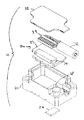
図2aおよび図2bを参照すると、リードヘッド4は、本体部20、蓋部22、プリント回路基板(PCB)アッセンブリ24、およびガラスプレート26を含み、ガラスプレート26の上に回折格子が形成されている。リードヘッド4が組み立てられると、PCBアッセンブリ24は、本体部20の中に着座し、蓋部22が、(たとえば、接着、溶接、圧着、または、スクリューなどのような追加的な機械的な手段を介して)本体部20に固定されており、PCBアッセンブリ24が本体部20の中に含有されるようになっている。PCBアッセンブリ24は、PCB27、ならびに、ケーブルコネクター34、インクリメンタルフォトディテクター36、リファレンスマークフォトディテクター38、光源40、および、PCB27の上に装着されている関連の処理電子機器を含む。そのうえ、示されているように、回折格子を含むガラスプレート26は、本体部の下側のウィンドウ領域28に装着されており、また、リードヘッド4へおよびリードヘッド4から信号およびパワーを運搬するためのケーブル32が、PCB27およびケーブル32の上の対応するコネクター34、39を介して、PCBアッセンブリ24に接続されている。
Referring to FIGS. 2a and 2b, the lead head 4 includes a main body 20, a lid 22, a printed circuit board (PCB)
インクリメンタルトラック10に関して、供給源40からの光は、回折格子を含有していないガラスプレート26の一部分を介してリードヘッド4を離れ、周期的なスケールマーク14の上に落ち、それは、回折パターンを画定する。したがって、光は、複数の次数へと回折し、それは、次いで、回折格子を含有するガラスプレート26の一部の上に落ちる。本実施形態では、リードヘッドの回折格子は、位相格子である。次いで、光は、リードヘッドの回折格子によって、次数へとさらに回折させられ、それは、次いで、インクリメンタルフォトディテクター36と干渉し、合成フィールド、このケースでは、干渉縞を形成する。
For the
干渉縞の発生は、図3および図4を参照してより詳細に説明される。理解されることとなるように、図3は、エンコーダー装置において遭遇する現実の光学的な状況に関する非常に簡単化された説明図である。とりわけ、供給源からの1つだけの光線に関する状況が示されているが、実際には、インクリメンタルトラック10の領域が、供給源によって照射されている。したがって、現実には、図3に示されている光学的な状況は、スケールの長さに沿って(すなわち、供給源によって照射される領域にわたって)何度も繰り返され、したがって、長い干渉パターンをディテクターに作り出し、それは、図4に概略的に図示されている。また、例示目的のために、+/−1次だけが示されている(たとえば、理解されることとなるように、光は、複数の次数、たとえば、+/−3次、+/−5次などの回折次数へと回折させられることとなる)。光は、スケール6のインクリメンタルトラック10の中の一連の周期的なフィーチャー14によって回折させられ、回折次数は、ガラスプレート26の上の回折格子に向けて伝搬し、インクリメンタルディテクター36において合成フィールド42(このケースでは、干渉縞であるが、たとえば、変調されたスポットであることが可能である)を形成する前に、ガラスプレート26の上の回折格子において、光が再び回折させられる。図4に示されているように、合成フィールド42は、ガラスプレート26の上の回折格子およびスケール6からの光の回折された次数の再組み合わせによって作り出される。
The occurrence of interference fringes will be described in more detail with reference to FIGS. 3 and 4. As will be appreciated, FIG. 3 is a very simplified explanatory view of the actual optical situation encountered in an encoder device. In particular, the situation with respect to only one ray from the source is shown, but in reality the region of the
インクリメンタルフォトディテクター36は、合成フィールド42(たとえば、干渉縞)を検出し、リードヘッド4によってコントローラー8などのような外部デバイスへケーブル32を介して出力される信号を作り出す。とりわけ、リードヘッド4およびスケール6の相対移動は、インクリメンタルディテクター36において、合成フィールドの変化(たとえば、ディテクター36に対する干渉縞の移動、または、変調されたスポットの強度の変化)を引き起こし、その出力は、インクリメンタルアップ/ダウンカウントを提供するように処理され得、インクリメンタルアップ/ダウンカウントは、変位のインクリメンタル測定を可能にする。
The
インクリメンタルディテクター36は、たとえば、複数のフォトダイオードを含むことが可能である。とりわけ、理解されることとなるように、干渉縞42がインクリメンタルディテクター36において作り出される実施形態では、インクリメンタルディテクター36は、電気格子の形態であることが可能であり、電気格子は、換言すれば、フォトセンサーアレイであり、フォトセンサーアレイは、たとえば、2つ以上のセットの交互配置で組み合わされた/インターレースされた感光センサーを含むことが可能であり、それぞれのセットが、ディテクター36において、干渉縞42の異なる位相を検出する。例が図5に図示されており、図5では、インクリメンタルディテクター36の一部が示されており、また、図5では、フォトダイオードA、B、C、およびDの4つのセットのフォトダイオードが交互配置で組み合わされており、セットの中のそれぞれのフォトダイオードからの出力が、単一の出力、A’、B’、C’、およびD’を提供するように組み合わせられている。図示されているように、(縞周期およびセンサー周期が同じである場合には、)時間の中の任意の1つの瞬間において、任意の1つのセットの中のすべてのフォトダイオードが、干渉縞の同じ位相の強度を検出する。このタイプのスケールおよびリードヘッドのより詳細が、特許文献4に説明されており、その内容全体が、参照により本明細書に組み込まれている。理解されることとなるように、電気格子/フォトセンサーアレイは、交互配置で組み合わされた3つだけのセットのフォトダイオードを含むことなどのような、他の形態をとることが可能であり、異なるレイアウトが使用され得る。
The
したがって、上記から理解され得るように、ガラスプレート26の上の回折格子とインクリメンタルフォトディテクター36との間の良好なアライメントを確実にすることが重要である可能性がある。これらのコンポーネント間の良好なアライメントを実現するための方法および装置が、図6から図11に関連して下記に説明されている。
Therefore, as can be understood from the above, it may be important to ensure good alignment between the grating on the
要約すれば、方法は、良好な信号を実現するために、動作時に使用されることとなる電気デバイスのセンサーから出力された信号を監視しながら(すなわち、このケースでは、インクリメンタルフォトディテクター36からの出力を監視しながら)、アライメント調整されることとなるコンポーネントのうちの少なくとも1つ(このケースでは、インクリメンタルフォトディテクター36をその上に備えるPCBアッセンブリ24)の位置を微調整することを含む(また、装置は、それを促進させる)。
In summary, the method monitors the signal output from the sensor of the electrical device that will be used during operation to achieve a good signal (ie, in this case, from the incremental photodetector 36). Includes (and in this case) fine-tuning the position of at least one of the components that will be aligned (in this case, the
したがって、図6から図11を参照すると、装置は、PCBアッセンブリ24をピックアップおよび移動させるためのマニピュレーター101を含む製造装置100(明確化の目的のために、その一部だけが示されている)を含む。マニピュレーターは、第1のグリッパー102、第2のグリッパー104、および第3のグリッパー106を含み、第1のグリッパー102がPCBアッセンブリ24の一方の縁部に係合することができるように、ならびに、第2のグリッパー104および第3のグリッパー106がPCBアッセンブリ24の反対側に係合することができるように、第1のグリッパー102、第2のグリッパー104、および第3のグリッパー106は構成されている。一緒になって、第1のもの102、第2のもの104および第3のもの106は、PCBアッセンブリ24を把持することが可能であり、PCBアッセンブリ24を保持および移動させるようになっている。また、マニピュレーターは、第1のスプリング付きの電気接点108、第2のスプリング付きの電気接点110、および第3のスプリング付きの電気接点112を含み、それらは、PCBアッセンブリ24の縁部の上に設けられた対応する電気接点に係合するためのものである。これらのスプリング付きの電気接点に加えて、電気接点が、第2のグリッパー104および第3のグリッパー106によって提供される。
Therefore, referring to FIGS. 6-11, the device is a manufacturing device 100 that includes a
製造装置100は、マニピュレーター101(および、したがって、マニピュレーターのグリッパー102、104、106によって保持されるPCBアッセンブリ24)を3つの直交する線形の次元X、Y、およびZに移動させるためのドライブ(図示せず)を含む。また、それは、マニピュレーター101を捩じるための、すなわち、Z軸線の周りに回転させるためのドライブを含む(随意的に、製造装置は、2つ以上の回転自由度でマニピュレーターを移動させるためのドライブを含むことが可能である)。この実施形態では、製造装置100は、マニピュレーター101の中に保持されたPCBアッセンブリ27を制御することが可能であり、Z軸線に対して平行な軸線の周りにそれを捩じる(すなわち、それを回転させる)ようになっている。また、製造装置100は、第1のグリッパー102、第2のグリッパー104、および第3のグリッパー106、ならびに、第1のスプリング付きの電気接点108、第2のスプリング付きの電気接点110、および第3のスプリング付きの電気接点112を移動させるためのドライブ(図示せず)を含み、PCBアッセンブリ24を選択的に係合/解放するようになっている。そのうえ、理解されることとなるように、製造装置100は、位置フィードバックデバイス(たとえば、位置測定エンコーダー)を含み、それは、マニピュレーター101の位置(および配向)、ならびに、したがって、マニピュレーター101によって保持されたPCBアッセンブリ27の位置(および配向)を決定するために使用され得る。
Manufacturing equipment 100 drives the manipulator 101 (and therefore the
また、製造装置100は、PCBアッセンブリ24がその中に位置付けされることとなる本体部20のためのホルダー(図示せず)と、マニピュレーター101(ならびに、したがって、本体部20およびPCBアッセンブリ24)に対してY次元およびZ次元にスケールエレメント114を保持および移動させるためのステージ(図示せず)とを含む。繰り返しになるが、位置報告デバイス(たとえば、位置測定エンコーダー)は、ステージ(および、したがって、スケールエレメント114)のY次元およびZ次元の位置を報告するために設けられている。
Further, the manufacturing apparatus 100 has a holder (not shown) for the main body 20 in which the
製造装置は、マニピュレーターの電気接点(すなわち、第1のスプリング付きの電気接点108、第2のスプリング付きの電気接点110、および第3のスプリング付きの電気接点112、ならびに、第2のグリッパー104および第3のグリッパー106によって提供される電気接点)へ/から、信号を送信および/または受信するためのプロセッサーデバイス(参照番号120によって概略的に図示されている)を含む。これは、有線リンクまたは無線リンクを介して行うことが可能である。また、同じプロセッサーデバイス120または異なるプロセッサーデバイスは、製造装置100、とりわけマニピュレーター101を制御するように構成され得る。
The manufacturing equipment includes the electrical contacts of the manipulator (ie, the
図10を参照すると、本発明によるプロセス200を図示するフローチャートが示されている。方法は、ステップ202において開始し、ステップ202において、プロセッサー120は、PCBアッセンブリ24をピックアップするようにマニピュレーター101を制御する。図6aによって図示されているように、これは、第1のグリッパー102、第2のグリッパー104、および第3のグリッパー106、ならびに、第1のスプリング付きの電気接点108、第2のスプリング付きの電気接点110、および第3のスプリング付きの電気接点112が、PCBアッセンブリ24(それは、ストレージポート(図示せず)の中に着座する)のいずれかの側に位置決めされるように、マニピュレーター101を位置決めすることを含み、また、次いで、図6bによって図示されているように、これは、第1のグリッパー102、第2のグリッパー104、および第3のグリッパー106、ならびに、第1のスプリング付きの電気接点108、第2のスプリング付きの電気接点110、および第3のスプリング付きの電気接点112を、それらがPCB27に係合するように、PCBアッセンブリ24に向けて前進させることを含む。PCB27は、その円周方向の縁部の上に電気接点パッドを有しており、それらは、第2のグリッパー104および第3のグリッパー106、ならびに、第1のスプリング付きの電気接点108、第2のスプリング付きの電気接点110、および第3のスプリング付きの電気接点112に係合するように位置付けされている。したがって、PCBアッセンブリのインクリメンタルフォトディテクター36に接続するステップ204が、同時に実現される。
With reference to FIG. 10, a flowchart illustrating the
説明されている例では、電気パワーは、第2のグリッパー104および第3のグリッパー106を介してPCBアッセンブリ24に供給されており、第1のスプリング付きの電気接点108、第2のスプリング付きの電気接点110、および第3のスプリング付きの電気接点112は、信号ラインである。たとえば、必ずというわけではないが、スプリング付きの電気接点のうちの1つ(たとえば、第1のスプリング付きの電気接点108)が、通信ラインとして(たとえば、PCBアッセンブリ24への、および/もしくは、PCBアッセンブリ24からのコマンドを通信するために、ならびに/または、PCBアッセンブリ24の一部として設けられた任意のメモリーデバイスへ/からデータを通信するために)使用され得、他の2つのスプリング付きの電気接点(たとえば、第2のスプリング付きの電気接点110および第3のスプリング付きの電気接点112)は、インクリメンタルフォトディテクター36からプロセッサーデバイス120へ信号を送信するために使用され得る。理解されることとなるように、さまざまな他の構成の信号ラインが存在することが可能である。たとえば、リードヘッド4およびたとえばPCBアッセンブリ24が自分自身のパワー供給源(たとえば、バッテリー)を含む実施形態では、パワー供給のための電気接点は、不必要である可能性が高い。そのうえ、いずれかの実施形態では、通信ラインが必要でない。さらには、いくつかのセンサーは、1つの信号出力だけを提供し、したがって、1つの信号ラインだけが必要になることとなる。また、理解されることとなるように、センサーがプロセッサーデバイスと無線で通信する実施形態は、本発明の範囲内であることとなり、したがって、物理的な電気接点が必要ないということが可能である。
In the example described, electrical power is supplied to the
簡潔に図11を参照すると、図示されているように、スプリング付きの電気接点(108、110、112)は、グリッパー(102、104、106)よりも長さが長い。そのうえ、PCBアッセンブリ24がマニピュレーター101によってピックアップされる前に、それは、台形の台座150を含むストレージポートの中に着座している。したがって、マニピュレーター101がPCBアッセンブリ24の上方に降ろされるときには、スプリング付きの電気接点が、台形の台座150の傾斜した側部によって、PCBアッセンブリから離れるように外へ押される。次いで、台形の台座150がスプリング付きの電気接点をPCB24から離れるように維持する間に、マニピュレーター101は、対向するグリッパーを引き合わせることが可能である。マニピュレーター101が台形の台座150から離れるようにそのストレージポートからPCBアッセンブリ24を持ち上げるときに、スプリング付きの電気接点は、それらの元の位置に向かって跳ね返り、それによって、PCBアッセンブリ24の縁部に係合する。そのような構成は、PCBアッセンブリ24をピックアップする途中に、スプリング付きの電気接点がPCBアッセンブリ24に衝突することを回避し、また、スプリング付きの電気接点がPCB27に力を及ぼす前にグリッパーがPCB27を良好に保持することを確実にする(それは、そうでなければ、マニピュレーター101の中のPCBアッセンブリ24の位置決めに影響を与える可能性がある)。理解されることとなるように、グリッパー102、104、106がPCB27を良好に保持するまで、スプリング付きの電気接点108、110、112がPCBアッセンブリ24に衝突せず、PCB27に接触しないことを確実にする他の方式が存在する。たとえば、PCBストレージポートは、ポケットを含むことが可能であり、マニピュレーター101がグリッパーおよびスプリング付きの電気接点をPCBアッセンブリ24に向けて降ろすときに、スプリング付きの電気接点108、110、112がポケットの中へスライドする。次いで、グリッパー102、104、106がPCB27を良好に保持し、マニピュレーター101がストレージポートからPCBアッセンブリ24を持ち上げるまで、ポケットは、PCB27に接触しないようにスプリング付きの電気接点108、110、112を保持することが可能である。
Briefly referring to FIG. 11, as shown, the spring-loaded electrical contacts (108, 110, 112) are longer than the grippers (102, 104, 106). Moreover, before the
図6cおよび図6dによって図示されているように、ステップ206において、マニピュレーター101は、PCBアッセンブリ24を移動させ、リードヘッドの本体部20の中にそれを位置付けするようになっている。本体部20は、マニピュレーター101の移動体積の中のポイントにおいて、ホルダー(図示せず)によって、測定装置100によって保持される。このポイントにおいて、本体部20は、蓋部22を有していないが、それは、そのウィンドウ領域28の中に装着された回折格子を含むガラスプレート26を有している。上記に説明されているように、および、図6c、図6d、および図7に図示されているように、回折格子を効果的に画定する周期的なフィーチャー(たとえば、使用時に、リードヘッド4がスケール6の上のインクリメンタルトラック10の中に見ることとなるようなもの)を有するスケールエレメント114が、ウィンドウ28、および、したがって、ガラスプレート26の下に位置付けされ、かつ、ステージ(図示せず)の上に装着されており、ステージは、スケールエレメント114をY次元におよびZ次元にも移動させるように駆動させられ得る。
As illustrated by FIGS. 6c and 6d, in
ステップ208において、PCBアッセンブリ24の位置が、マニピュレーター101によって微調整される。要約すれば、これは、第2のグリッパー104および第3のグリッパー106によって提供される電気接点を介してPCBアッセンブリ24にパワーを与えることを含み、光源40が活性化させられ、スケールエレメント114を照射するようになっている。このケースでは干渉縞の形態の合成フィールドが、次いで、図3および図4に関連して上記に説明されている様式で、インクリメンタルフォトディテクター36の上に作り出される。インクリメンタルフォトディテクター36は、干渉縞の検出に応答して信号を作り出し、干渉縞は、スケールエレメント114の移動とともに変化する。そのような信号は、第2のスプリング付きの電気接点110および第3のスプリング付きの電気接点112を介して、分析のためにプロセッサー120に渡される。要約すれば、本発明による方法は、プロセッサー120のプロセスを含み、プロセッサー120は、インクリメンタルフォトディテクター36から信号を受信し、スケールエレメント114がY次元に移動させられている間に信号を解析する。(たとえば、所望の振幅の)所望の信号がインクリメンタルフォトディテクターから取得されるまで、PCBアッセンブリ24の位置が微調整される。
In
1つの特定の実施形態では、方法は、Z次元、および、また、そのヨー配向(すなわち、Z軸線に平行なPCB27の中心を通る軸線の周りのその角度配向)において、PCBアッセンブリ24の位置決め/微調整(たとえば、ファインチューニング)を支援するためだけに、インクリメンタルフォトディテクター36センサーからの出力を使用することを含む。とりわけ、方法は、リードヘッドの本体部20の中の初期の位置および配向においてPCBアッセンブリ24を位置決めすることを含むことが可能である。初期の位置におけるPCBアッセンブリ24のZ位置/高さは、高過ぎると予期される高さに設定され得る。実際に、これが低過ぎ、および、したがって、PCB27が、本体部20のベースに衝突するケースに備えて、ならびに/または、PCB27が、PCB27と本体部20のベースとの間の任意の事前塗布された接着剤(それは、最終的には、PCBアッセンブリ24を本体部20に留めるために使用される)があまりにも薄く圧迫されることを引き起こすケースに備えて、最終的な所望の高さであると予期され得る高さにPCBアッセンブリ24を最初に設置しないことが有利である可能性がある。
In one particular embodiment, the method positions the
次いで、方法は、スケールエレメント114をY次元に移動させることと、プロセッサー120がインクリメンタルフォトディテクター36からの信号を監視することとを含むことが可能である。次いで、プロセッサー120がインクリメンタルフォトディテクター36からの信号を監視する間に、スケールエレメント114のZ位置/高さが調節され、次いで、再びY次元に移動させられ得る。これは、スケールエレメント114の複数の異なる高さに関して繰り返され得る。異なる高さに関するインクリメンタルフォトディテクター36の出力が分析され、本体部20に対するPCBアッセンブリ24の高さをどのように調節するかということを決定し(たとえば、PCBアッセンブリ24が本体部20の中へどれだけ低下させられるべきであるかということを決定し)、それが最終的に使用されることとなる、リードヘッド20の好適なライド(ride)高さにおいて良好な信号を実現することが可能である。次いで、本体部20に対するPCBアッセンブリ24の高さは、マニピュレーター101によって変化させられ得る。
The method can then include moving the scale element 114 in the Y dimension and the
次いで、本体部の中のPCBアッセンブリ24の異なるヨー配向のために、Y次元に沿ってスケールエレメント114を移動させる(それは、ヨー配向を制御するマニピュレーター101によって実現され得る)ことによって、および、インクリメンタルフォトディテクター36からの信号を監視することによって、PCBアッセンブリ24のヨー配向が微調整され得る。次いで、異なるヨー配向のためにインクリメンタルフォトディテクター36の出力が分析され、本体部20に対してどのヨー配向にPCBアッセンブリ24を設定するかということを決定することが可能である。
The scale element 114 is then moved along the Y dimension for different yaw orientations of the
望まれる場合には、スケールエレメント114の異なるZ位置のために、インクリメンタルフォトディテクター36の出力を監視することによって、PCBアッセンブリ24の高さが、再びチェックされ得る。
If desired, the height of the
この実施形態では、X、Y横方向位置、ならびに、ピッチおよびロール配向(XおよびY軸線に平行な軸線の周りの角度配向)は、本発明の方法によって調節/微調整されない。むしろ、マニピュレーターが本体部20に対してPCBアッセンブリ24をそれらの次元/配向に正しく位置決め/配向させていると仮定することによって、それらは設定されている。本例では、そのような仮定は、それらの次元/配向におけるPCBアッセンブリ24の一般的な位置/配向が(マニピュレーター101/製造装置100の上の位置フィードバックデバイスからのフィードバックを使用して)マニピュレーター101および本体部20の位置の知識から決定され得るということによって左右され得、本体部20は、測定装置100のホルダーによって(すなわち、固定された位置に)保持されている。理解されることとなるように、PCBアッセンブリ24がマニピュレーターのグリッパー102、104、106によって保持される正確な位置の中に、いくらかの不確実性が存在する可能性がある。そのような場合には、カメラが使用され、PCBアッセンブリ24がマニピュレーター101によってピックアップされるとPCBアッセンブリ24をイメージ化し/見ることが可能であり、そのXおよびY位置が決定され得るようになっている。また、特に、カメラが相対的に幅の狭い被写界深度を有する場合には、カメラは、マニピュレーター101に対するPCBアッセンブリ24の概算的なZ位置を提供することが可能である。
In this embodiment, the X, Y lateral positions, as well as the pitch and roll orientations (angle orientations around the axes parallel to the X and Y axes) are not adjusted / finely adjusted by the methods of the invention. Rather, they are set by assuming that the manipulator correctly positions / aligns the
そのうえ、本例では、説明されているリードヘッドのタイプの精度は、XおよびY次元(または、そのピッチ配向およびロール配向)におけるPCBアッセンブリ24のインクリメンタルフォトディテクター36の設置に対して、Z次元およびヨー配向におけるその設置および配向に対するものほど敏感ではなく、したがって、XおよびY位置、ならびに、ピッチおよびロール配向にPCBを微調整/ファインチューニングすることは、Zおよびヨーの自由度におけるPCBの微調整/ファインチューニングほど重要ではない。
Moreover, in this example, the accuracy of the leadhead types described is Z-dimensional and relative to the installation of the
上記に説明されているように、インクリメンタルフォトディテクター36からの信号が監視/分析される。理解されることとなるように、信号がインクリメンタルフォトディテクター36から出力されるときに、信号は分析され得る。随意的に、信号は、その後のポイントにおいて、たとえば、相対的な異なる高さ/配向においてすべての関連の信号が取得された後に、メモリーの中に記録され、分析され得る。
As described above, the signal from the
また、理解されることとなるように、正確に、信号のどの態様が分析されるかということは、製造されている電子デバイスのタイプ、電子デバイスのセンサーによって出力される信号のタイプ、および/または、センサーもしくは他のコンポーネントが正確にどの程度精密に位置決めされる必要があるかということを含む、特定のさまざまな要因に依存する可能性がある。たとえば、方法は、信号の振幅を見ることを含むことが可能である。 Also, as will be understood, exactly which aspect of the signal is analyzed depends on the type of electronic device being manufactured, the type of signal output by the sensor of the electronic device, and /. Alternatively, it may depend on a variety of specific factors, including exactly how precisely the sensor or other component needs to be positioned. For example, the method can include looking at the amplitude of the signal.
本例では、インクリメンタルフォトディテクター36は、互いから90°位相がずれた(理想的には)2つの一般的な正弦波を出力し、それは、一般に直交信号と称される。そのような信号は、リサージュを作り出すために使用され得、信号の1つの実装形態が使用され、インクリメンタルフォトディテクターの直交信号によって作り出されるリサージュの半径を決定すること、および、所望の公差バンドの中の半径が実現されるまで、少なくとも1つの自由度における位置および/または配向を微調整することが可能である。
In this example, the
信号が所定の基準を満たす位置にPCBアッセンブリ24があるということをプロセッサー120が決定すると、PCBアッセンブリ24が、適切な場所に固定される。たとえば、これは、たとえば、PCB27と本体部20のベースとの間に以前に適用され得たPCB27を適切な場所に接着することによって、および、たとえば、本体部20のベースとPCB27との間の接着剤にUV光を方向付けすることによってUV硬化性の接着剤を硬化させることによって、実現され得る。UV光を介してそのように硬化させることを支援するために、孔部/ウィンドウ/UV透過領域などが、PCBの中に、特に、接着剤が位置付けされている領域に設けられ得、UV光が、接着剤を硬化させるために、PCBを通って照らされ得るようになっている。
When the
PCBアッセンブリ24が本体部20に固定されると、プロセッサーデバイス120は、マニピュレーター101を制御し、それがグリッパー102、104、106およびスプリング付きの電気接点108、110、112を後退させることを引き起こし、マニピュレーター101からPCBアッセンブリ24を解放するようになっている。次いで、ケーブル32が、PCBコネクター34に接続され得、蓋部22が、本体部20に適用され得る(それは、たとえば、同じ製造装置100、異なる製造装置、または人間によって行われ得る)。
When the
説明されている実施形態では、グリッパーおよびスプリング付きの電気接点が、同じ次元においてPCB27に対して付勢される。これは、グリッパーおよびスプリング付きの電気接点が互いに争う(それは、PCB27の逆移動につながる可能性がある)ことにならないことを確実にする。そのうえ、電気接点およびグリッパーは、PCB27を横切って横方向に、および、とりわけ、PCB27の平面的な面同士の間に延在する縁部に対抗して、付勢される。これは、PCB27の平面的な面の上の貴重なスペースを使い尽くさなければならないということを回避し、したがって、PCB27のサイズを最小に維持することを助ける。しかし、理解されることとなるように、これは、必ずしもそうである必要はない。たとえば、マニピュレーターは、PCB27の平面的な面のうちの少なくとも1つの上に設けられた接点に係合する電気接点ピンを有することが可能である。随意的に、グリッパーは、PCB27の平面的な面に係合することが可能である。 In the embodiments described, grippers and spring-loaded electrical contacts are urged against the PCB 27 in the same dimension. This ensures that the gripper and spring-loaded electrical contacts do not compete with each other (which can lead to reverse movement of the PCB 27). Moreover, the electrical contacts and grippers are urged laterally across the PCB 27 and, above all, against the edges extending between the planar surfaces of the PCB 27. This avoids having to run out of valuable space on the flat surface of the PCB 27 and thus helps keep the size of the PCB 27 to a minimum. But, as will be understood, this does not necessarily have to be the case. For example, the manipulator can have electrical contact pins that engage contacts provided on at least one of the planar surfaces of the PCB 27. Optionally, the gripper can engage the planar surface of the PCB 27.
説明されている実施形態では、インクリメンタルフォトディテクター36からの信号は、第1のスプリング付きの電気接点108、第2のスプリング付きの電気接点110、および第3のスプリング付きの電気接点112を介して提供される電気接点を介して、プロセッサーデバイス120に伝達される。理解されることとなるように、これは、必ずしもそうである必要はない。たとえば、PCBアッセンブリ24は、プロセッサーデバイス120に信号を無線で送るための無線送信器を含むことが可能である。このケースでは、パワーは、PCBに係合するマニピュレーター101によって提供される電気接点を介して、PCBアッセンブリ24に供給され得る。随意的に、PCBアッセンブリ24は、光源、センサー、および、任意の無線送信器を含む、PCBアッセンブリ24にパワーを与えるためのバッテリーを含むことが可能である。
In the embodiments described, the signal from the
随意的に、データは、PCB27の上のメモリーデバイスとプロセッサーデバイス120(または、実際に別のプロセッサーデバイス)との間で伝達され得る。たとえば、データ(たとえば、リードヘッドの製造または使用の間に使用するためのデータ)は、PCB27の上のメモリーデバイスの中へロードされ得る(または、実際には、PCB27の上のメモリーデバイスから抽出され得る)。そのようなデータのタイプの例は、製造番号、部品番号、キャリブレーションデータ、製造日を含む。 Optionally, data can be transmitted between the memory device on the PCB 27 and the processor device 120 (or actually another processor device). For example, data (eg, data for use during readhead manufacturing or use) can be loaded into (or is actually extracted from) a memory device on the PCB27. Can be). Examples of such data types include serial number, part number, calibration data, date of manufacture.
上記に説明されている実施形態では、PCBアッセンブリ24の位置は、マニピュレーター101によって操作されている。しかし、理解されることとなるように、単にインクリメンタルフォトディテクター36の位置だけが調節され得、次いで、所望の位置が見出されたときに、それはPCB27に固定され得、PCB27は、前もって本体部に装着されていてもよい。随意的に、インデックスグレーティングを含むガラスプレート26の位置は、PCBアッセンブリ24の代わりに、または、PCBアッセンブリ24とともに、操作され得る。すべてのケースにおいて、インクリメンタルフォトディテクター36からの信号は、インクリメンタルフォトディテクター36およびガラスプレート26の好適な相対位置を決定するために使用され得る。
In the embodiments described above, the position of the
上記に説明されている実施形態では、位置エンコーダーが、インクリメンタルエンコーダーである。それにもかかわらず、理解されることとなるように、本発明は、アブソリュートエンコーダーを含む、他のタイプの位置エンコーダーにも適用可能である。たとえば、特許文献3に説明されているものを含む、多くのアブソリュートエンコーダーは、スケールのイメージを検出するためにレンズを使用する。本発明は、たとえば、イメージングレンズとイメージセンサーとの間のアライメントを支援するのに有用である可能性がある。 In the embodiments described above, the position encoder is an incremental encoder. Nevertheless, as will be appreciated, the present invention is also applicable to other types of position encoders, including absolute encoders. For example, many absolute encoders, including those described in Patent Document 3, use a lens to detect an image of scale. The present invention may be useful, for example, to assist in alignment between an imaging lens and an image sensor.
上記の実施形態では、電気デバイスは、光学的な位置測定エンコーダー装置のためのリードヘッドである。また、理解されることとなるように、本発明は、磁気的なおよび容量性の位置測定エンコーダーを含む、他のタイプの位置測定エンコーダーなどのような他の電気デバイスの製造を支援するために使用され得る。他の例は、温度センサー、圧力センサー、プローブ、たとえば、測定プローブ、とりわけ、座標測定機(CMM)および工作機械などのような座標位置決め装置の上で使用されるタイプなどのような位置測定プローブなどのような、他のタイプのセンサーを含む。 In the above embodiment, the electrical device is a leadhead for an optical position measuring encoder device. Also, as will be appreciated, the present invention is to assist in the manufacture of other electrical devices, such as other types of position measuring encoders, including magnetic and capacitive position measuring encoders. Can be used. Other examples are temperature sensors, pressure sensors, probes, such as measuring probes, especially positioning probes such as the type used on coordinate positioning devices such as coordinate measuring machines (CMMs) and machine tools. Includes other types of sensors, such as.
また、本発明者は、(たとえ、上記の実施形態のもののようなセンサーに接続していなくても、)製造の間にその位置が操作されながら、PCBなどのような電子コンポーネントへの電気的な接続を提供することが有用であることを見出した。たとえば、最終製品への組み立ての前にPCB27/PCBアッセンブリ24の機能をテストすることが有用である可能性がある。また、電子コンポーネントをプログラムすること、または、電子コンポーネントからの他のデータを抽出/構築/テストすることが、有用である可能性がある。とりわけ、PCBに接続するとき、PCBの縁部の上に提供される接点を介して接続することは、有利である可能性がある。その理由は、それが、PCBスペースを節約し、コストを低減させ、また、PCBの変形を回避するのを助けることが可能であるからである。
Also, the inventor (even if not connected to a sensor as in the above embodiment) can electrically manipulate electronic components such as PCBs while manipulating their position during manufacturing. We have found it useful to provide a good connection. For example, it may be useful to test the functionality of the PCB 27 /
Claims (13)
前記センサーからの出力を使用して前記リードヘッドの少なくとも1つのコンポーネントおよび前記少なくとも1つのセンサーをお互いに対して位置決めするステップであって、前記センサーからの出力を使用して、前記センサーおよび/または前記少なくとも1つのコンポーネントの相対的な場所を微調整することを含むステップ
を含み、
前記少なくとも1つのコンポーネントは、光学コンポーネントを含み、前記方法は、前記センサーを保持しおよび移動させるアクチュエーターと、前記センサーからの前記出力を使用して、前記センサーの位置決めをするように前記アクチュエーターの運動を制御するプロセッサーデバイスと、を含む製造装置の使用を含むことを特徴とする方法。 A method of manufacturing a measurement device that includes a leadhead for a position measurement encoder device, wherein the leadhead comprises at least one sensor.
The output from the sensor is used to position at least one component of the leadhead and the at least one sensor with respect to each other, and the output from the sensor is used to position the sensor and / or the sensor. Includes steps involving fine-tuning the relative location of at least one component.
The at least one component includes an optical component, the method of which uses an actuator to hold and move the sensor and the output from the sensor to move the actuator to position the sensor. A method comprising the use of a processor device to control and a manufacturing apparatus including.
前記少なくとも1つのグリッパーおよび少なくとも1つの電気コネクターは、前記PCBに対抗して同じ方向に付勢されることを特徴とする請求項8に記載の方法。 The actuator comprises at least one gripper for engaging the component.
8. The method of claim 8, wherein the at least one gripper and at least one electrical connector are urged in the same direction against the PCB.
Applications Claiming Priority (3)
| Application Number | Priority Date | Filing Date | Title |
|---|---|---|---|
| EP13275239.5 | 2013-10-01 | ||
| EP13275239 | 2013-10-01 | ||
| PCT/EP2014/070621 WO2015049175A1 (en) | 2013-10-01 | 2014-09-26 | Method of manufacturing an electronic component |
Publications (3)
| Publication Number | Publication Date |
|---|---|
| JP2016536577A JP2016536577A (en) | 2016-11-24 |
| JP2016536577A5 JP2016536577A5 (en) | 2019-03-28 |
| JP6811610B2 true JP6811610B2 (en) | 2021-01-13 |
Family
ID=49301403
Family Applications (1)
| Application Number | Title | Priority Date | Filing Date |
|---|---|---|---|
| JP2016519751A Active JP6811610B2 (en) | 2013-10-01 | 2014-09-26 | How to manufacture electronic components |
Country Status (6)
| Country | Link |
|---|---|
| US (1) | US20160238415A1 (en) |
| EP (1) | EP3052895B1 (en) |
| JP (1) | JP6811610B2 (en) |
| CN (1) | CN106030251B (en) |
| ES (1) | ES2881544T3 (en) |
| WO (1) | WO2015049175A1 (en) |
Families Citing this family (2)
| Publication number | Priority date | Publication date | Assignee | Title |
|---|---|---|---|---|
| US10303270B2 (en) * | 2016-09-12 | 2019-05-28 | Microsoft Technology Licensing, Llc | Linear encoder force transducer |
| CN111200925A (en) * | 2019-12-31 | 2020-05-26 | 南京沃联科技有限公司 | Antistatic SMT feeding and discharging rack |
Family Cites Families (26)
| Publication number | Priority date | Publication date | Assignee | Title |
|---|---|---|---|---|
| US4593820A (en) * | 1984-03-28 | 1986-06-10 | International Business Machines Corporation | Robotic, in-transit, device tester/sorter |
| JPH0385523U (en) * | 1989-12-20 | 1991-08-29 | ||
| GB9424969D0 (en) | 1994-12-10 | 1995-02-08 | Renishaw Plc | Opto-electronic scale reading apparatus |
| JPH11101660A (en) * | 1997-09-26 | 1999-04-13 | Mitsutoyo Corp | Optical displacement detection device |
| JP2002081962A (en) * | 2000-09-06 | 2002-03-22 | Seiko Instruments Inc | Rotary angle detector |
| GB0109057D0 (en) | 2001-04-11 | 2001-05-30 | Renishaw Plc | Absolute postition measurement |
| JP2003279379A (en) * | 2002-03-26 | 2003-10-02 | Citizen Watch Co Ltd | Optical displacement measuring instrument |
| JP3990591B2 (en) * | 2002-04-18 | 2007-10-17 | 株式会社仙台ニコン | Encoder |
| DE10329374A1 (en) * | 2003-06-30 | 2005-01-20 | Dr. Johannes Heidenhain Gmbh | Scanning unit of a position measuring device |
| JP3963885B2 (en) * | 2003-10-27 | 2007-08-22 | オリンパス株式会社 | Reflective optical encoder sensor head |
| JP4416544B2 (en) * | 2004-03-12 | 2010-02-17 | 株式会社ミツトヨ | Optical displacement measuring device |
| JP4418278B2 (en) * | 2004-03-30 | 2010-02-17 | オリンパス株式会社 | Optical encoder and manufacturing method thereof |
| GB0413710D0 (en) | 2004-06-21 | 2004-07-21 | Renishaw Plc | Scale reading apparatus |
| US9104650B2 (en) * | 2005-07-11 | 2015-08-11 | Brooks Automation, Inc. | Intelligent condition monitoring and fault diagnostic system for preventative maintenance |
| GB2444464B (en) * | 2005-11-09 | 2010-08-25 | Gsi Group Corp | Scale assembly for optical encoder having affixed optical reference markers |
| JP2008232705A (en) * | 2007-03-19 | 2008-10-02 | Mitsutoyo Corp | Photoelectric encoder |
| JP2008256392A (en) * | 2007-04-02 | 2008-10-23 | Matsushita Electric Ind Co Ltd | Optical encoder assembly method |
| DE102007018048A1 (en) * | 2007-04-13 | 2008-10-16 | Michael Schwertner | Method and arrangement for optical imaging with depth discrimination |
| JP5052391B2 (en) * | 2008-04-11 | 2012-10-17 | オリンパス株式会社 | Optical encoder |
| JP4960308B2 (en) * | 2008-06-12 | 2012-06-27 | 富士フイルム株式会社 | Image sensor position adjusting method, camera module manufacturing method and apparatus |
| GB0819767D0 (en) | 2008-10-28 | 2008-12-03 | Renishaw Plc | Absolute encoder setup indication |
| DE102008062561A1 (en) * | 2008-12-16 | 2010-06-24 | Maxon Motor Ag | Kit for an electric motor with a rotary encoder |
| JP5484980B2 (en) * | 2010-03-24 | 2014-05-07 | 株式会社ミツトヨ | Optical encoder |
| JP5692584B2 (en) * | 2011-02-15 | 2015-04-01 | 株式会社安川電機 | Servo motor manufacturing method, servo motor manufacturing apparatus, servo motor, encoder |
| US20130001412A1 (en) * | 2011-07-01 | 2013-01-03 | Mitutoyo Corporation | Optical encoder including passive readhead with remote contactless excitation and signal sensing |
| JP5896804B2 (en) * | 2012-03-26 | 2016-03-30 | 三菱電機株式会社 | Readhead control mechanism and optical encoder |
-
2014
- 2014-09-26 EP EP14776657.0A patent/EP3052895B1/en active Active
- 2014-09-26 WO PCT/EP2014/070621 patent/WO2015049175A1/en active Application Filing
- 2014-09-26 US US15/025,398 patent/US20160238415A1/en not_active Abandoned
- 2014-09-26 JP JP2016519751A patent/JP6811610B2/en active Active
- 2014-09-26 CN CN201480065546.3A patent/CN106030251B/en active Active
- 2014-09-26 ES ES14776657T patent/ES2881544T3/en active Active
Also Published As
| Publication number | Publication date |
|---|---|
| US20160238415A1 (en) | 2016-08-18 |
| WO2015049175A1 (en) | 2015-04-09 |
| CN106030251A (en) | 2016-10-12 |
| ES2881544T3 (en) | 2021-11-29 |
| EP3052895B1 (en) | 2021-06-16 |
| EP3052895A1 (en) | 2016-08-10 |
| CN106030251B (en) | 2019-02-01 |
| JP2016536577A (en) | 2016-11-24 |
Similar Documents
| Publication | Publication Date | Title |
|---|---|---|
| CN103256890B (en) | Contact type probe | |
| CN101551233B (en) | Workpiece size detecting device | |
| CN109754425B (en) | Calibration equipment and calibration method of TOF (time of flight) camera module | |
| CN102197282B (en) | Absolute encoder setup indication | |
| US8965577B2 (en) | Force sensor and industrial robot including the same | |
| EP1195615B1 (en) | Position determining system | |
| CN100507454C (en) | Scale and readhead apparatus | |
| US7027160B2 (en) | Device and method for measuring transmission and reflection properties of objects and surfaces | |
| JP2008524631A (en) | Method and apparatus for measuring the thickness of a thin film | |
| US11169009B2 (en) | Encoder apparatus, robot apparatus, and method for measuring gap | |
| US11061338B2 (en) | High-resolution position encoder with image sensor and encoded target pattern | |
| JP6811610B2 (en) | How to manufacture electronic components | |
| KR20190075144A (en) | Next generation bending measurement system | |
| CN104142132A (en) | Device for determining the location of mechanical elements | |
| CN111795713A (en) | Optical encoder | |
| TWI474003B (en) | Optical accelerometer | |
| WO2007027960A2 (en) | Substrate alignment using linear array sensor | |
| KR101854177B1 (en) | Processing implement position alignment device for component and method thereof | |
| CN102607470A (en) | Non-contact automatic detection device for straightness errors of milling surface of scale grating of grating ruler | |
| CN105988309A (en) | Alignment device for lithography equipment and alignment method | |
| JP2022087326A (en) | Encoder | |
| KR101941902B1 (en) | Measuring device and method for triangulation measurement | |
| JP6462248B2 (en) | Length measuring device, displacement amount calculating means, and alignment method between scale portion and pattern reading portion of length measuring device | |
| KR101377687B1 (en) | Optical encoder mixed incremental type and absolute type | |
| JP7096009B2 (en) | Manufacturing method of position detection encoder and position detection encoder |
Legal Events
| Date | Code | Title | Description |
|---|---|---|---|
| A521 | Request for written amendment filed |
Free format text: JAPANESE INTERMEDIATE CODE: A523 Effective date: 20170925 |
|
| A621 | Written request for application examination |
Free format text: JAPANESE INTERMEDIATE CODE: A621 Effective date: 20170925 |
|
| A977 | Report on retrieval |
Free format text: JAPANESE INTERMEDIATE CODE: A971007 Effective date: 20180731 |
|
| A131 | Notification of reasons for refusal |
Free format text: JAPANESE INTERMEDIATE CODE: A131 Effective date: 20180814 |
|
| A601 | Written request for extension of time |
Free format text: JAPANESE INTERMEDIATE CODE: A601 Effective date: 20181112 |
|
| A524 | Written submission of copy of amendment under article 19 pct |
Free format text: JAPANESE INTERMEDIATE CODE: A524 Effective date: 20190214 |
|
| A131 | Notification of reasons for refusal |
Free format text: JAPANESE INTERMEDIATE CODE: A131 Effective date: 20190709 |
|
| A601 | Written request for extension of time |
Free format text: JAPANESE INTERMEDIATE CODE: A601 Effective date: 20191004 |
|
| A521 | Request for written amendment filed |
Free format text: JAPANESE INTERMEDIATE CODE: A523 Effective date: 20191223 |
|
| A02 | Decision of refusal |
Free format text: JAPANESE INTERMEDIATE CODE: A02 Effective date: 20200428 |
|
| A521 | Request for written amendment filed |
Free format text: JAPANESE INTERMEDIATE CODE: A523 Effective date: 20200828 |
|
| C60 | Trial request (containing other claim documents, opposition documents) |
Free format text: JAPANESE INTERMEDIATE CODE: C60 Effective date: 20200828 |
|
| A911 | Transfer to examiner for re-examination before appeal (zenchi) |
Free format text: JAPANESE INTERMEDIATE CODE: A911 Effective date: 20200909 |
|
| C21 | Notice of transfer of a case for reconsideration by examiners before appeal proceedings |
Free format text: JAPANESE INTERMEDIATE CODE: C21 Effective date: 20200915 |
|
| TRDD | Decision of grant or rejection written | ||
| A01 | Written decision to grant a patent or to grant a registration (utility model) |
Free format text: JAPANESE INTERMEDIATE CODE: A01 Effective date: 20201117 |
|
| A61 | First payment of annual fees (during grant procedure) |
Free format text: JAPANESE INTERMEDIATE CODE: A61 Effective date: 20201215 |
|
| R150 | Certificate of patent or registration of utility model |
Ref document number: 6811610 Country of ref document: JP Free format text: JAPANESE INTERMEDIATE CODE: R150 |
|
| R250 | Receipt of annual fees |
Free format text: JAPANESE INTERMEDIATE CODE: R250 |