JP6807829B2 - Systems and methods for simultaneous darkfield and phase contrast inspection - Google Patents
Systems and methods for simultaneous darkfield and phase contrast inspection Download PDFInfo
- Publication number
- JP6807829B2 JP6807829B2 JP2017503491A JP2017503491A JP6807829B2 JP 6807829 B2 JP6807829 B2 JP 6807829B2 JP 2017503491 A JP2017503491 A JP 2017503491A JP 2017503491 A JP2017503491 A JP 2017503491A JP 6807829 B2 JP6807829 B2 JP 6807829B2
- Authority
- JP
- Japan
- Prior art keywords
- signal
- sample
- illumination
- sensor
- path
- Prior art date
- Legal status (The legal status is an assumption and is not a legal conclusion. Google has not performed a legal analysis and makes no representation as to the accuracy of the status listed.)
- Active
Links
- 238000007689 inspection Methods 0.000 title claims description 36
- 238000000034 method Methods 0.000 title claims description 19
- 238000005286 illumination Methods 0.000 claims description 122
- 210000001747 pupil Anatomy 0.000 claims description 59
- 230000003287 optical effect Effects 0.000 claims description 55
- 238000000926 separation method Methods 0.000 claims description 15
- 238000005259 measurement Methods 0.000 claims description 3
- 238000007499 fusion processing Methods 0.000 claims description 2
- 239000000523 sample Substances 0.000 claims 23
- 239000012472 biological sample Substances 0.000 claims 3
- 230000007547 defect Effects 0.000 description 24
- 238000001514 detection method Methods 0.000 description 7
- 238000010586 diagram Methods 0.000 description 7
- 239000004065 semiconductor Substances 0.000 description 5
- 235000012431 wafers Nutrition 0.000 description 5
- 230000008901 benefit Effects 0.000 description 4
- 238000012360 testing method Methods 0.000 description 4
- 238000012512 characterization method Methods 0.000 description 3
- 230000004927 fusion Effects 0.000 description 3
- 230000001902 propagating effect Effects 0.000 description 3
- 238000003860 storage Methods 0.000 description 3
- 238000004458 analytical method Methods 0.000 description 2
- 238000003384 imaging method Methods 0.000 description 2
- 238000004519 manufacturing process Methods 0.000 description 2
- 238000012544 monitoring process Methods 0.000 description 2
- 239000002245 particle Substances 0.000 description 2
- 238000012545 processing Methods 0.000 description 2
- 241000269350 Anura Species 0.000 description 1
- 238000013459 approach Methods 0.000 description 1
- 230000009286 beneficial effect Effects 0.000 description 1
- 238000004140 cleaning Methods 0.000 description 1
- 238000005530 etching Methods 0.000 description 1
- 230000006870 function Effects 0.000 description 1
- 238000005468 ion implantation Methods 0.000 description 1
- 238000001459 lithography Methods 0.000 description 1
- 238000012986 modification Methods 0.000 description 1
- 230000004048 modification Effects 0.000 description 1
- 238000007747 plating Methods 0.000 description 1
- 238000005498 polishing Methods 0.000 description 1
- 230000000644 propagated effect Effects 0.000 description 1
- 230000001629 suppression Effects 0.000 description 1
Images


Classifications
-
- G—PHYSICS
- G01—MEASURING; TESTING
- G01N—INVESTIGATING OR ANALYSING MATERIALS BY DETERMINING THEIR CHEMICAL OR PHYSICAL PROPERTIES
- G01N21/00—Investigating or analysing materials by the use of optical means, i.e. using sub-millimetre waves, infrared, visible or ultraviolet light
- G01N21/84—Systems specially adapted for particular applications
- G01N21/88—Investigating the presence of flaws or contamination
- G01N21/8806—Specially adapted optical and illumination features
-
- G—PHYSICS
- G01—MEASURING; TESTING
- G01N—INVESTIGATING OR ANALYSING MATERIALS BY DETERMINING THEIR CHEMICAL OR PHYSICAL PROPERTIES
- G01N21/00—Investigating or analysing materials by the use of optical means, i.e. using sub-millimetre waves, infrared, visible or ultraviolet light
- G01N21/84—Systems specially adapted for particular applications
- G01N21/88—Investigating the presence of flaws or contamination
- G01N21/95—Investigating the presence of flaws or contamination characterised by the material or shape of the object to be examined
- G01N21/9501—Semiconductor wafers
-
- G—PHYSICS
- G01—MEASURING; TESTING
- G01N—INVESTIGATING OR ANALYSING MATERIALS BY DETERMINING THEIR CHEMICAL OR PHYSICAL PROPERTIES
- G01N21/00—Investigating or analysing materials by the use of optical means, i.e. using sub-millimetre waves, infrared, visible or ultraviolet light
- G01N21/84—Systems specially adapted for particular applications
- G01N21/88—Investigating the presence of flaws or contamination
- G01N21/8806—Specially adapted optical and illumination features
- G01N2021/8822—Dark field detection
- G01N2021/8825—Separate detection of dark field and bright field
Landscapes
- Physics & Mathematics (AREA)
- Health & Medical Sciences (AREA)
- Life Sciences & Earth Sciences (AREA)
- Chemical & Material Sciences (AREA)
- Analytical Chemistry (AREA)
- Biochemistry (AREA)
- General Health & Medical Sciences (AREA)
- General Physics & Mathematics (AREA)
- Immunology (AREA)
- Pathology (AREA)
- Investigating Materials By The Use Of Optical Means Adapted For Particular Applications (AREA)
- Microscoopes, Condenser (AREA)
- Investigating Or Analysing Materials By Optical Means (AREA)
- Testing Or Measuring Of Semiconductors Or The Like (AREA)
Description
本発明は一般に欠陥の検出と分類に関し、より具体的には、同時の暗視野検査と微分干渉コントラストの検査に関する。 The present invention generally relates to defect detection and classification, and more specifically to simultaneous darkfield inspection and differential interference contrast inspection.
関連出願への相互参照
本出願は、その全体を本明細書に参照により組み込む、2014年7月22日に出願された、「暗視野および位相コントラストの同時検査のための装置および方法」というタイトルの、Chuanyong Huang、Qing Li、Donald PettiboneおよびBuzz Gravesを発明者とした米国特許仮出願第62/027,393号の利益を、米国特許法第119条(e)に基づき主張する。
Cross-references to related applications This application is incorporated herein by reference in its entirety, entitled "Devices and Methods for Simultaneous Inspection of Dark Field and Phase Contrast," filed July 22, 2014. Claims the benefit of U.S. Patent Application No. 62 / 027,393, invented by Chuanyong Hung, Qing Li, Donald Pettibone and Buzz Graves, under Article 119 (e) of the U.S. Patent Act.
半導体デバイス製造プロセスへの許容差が狭くなり続けるにつれ、改良された半導体ウェーハ検査ツールへの要求が増加し続けている。ウェーハ検査に適した検査ツールのタイプは、試料(例えば半導体ウェーハ)からの散乱情報を利用する暗視野(DF)検査ツールと、試料からの位相情報を利用する微分干渉コントラスト検査ツールを含む。一般に、DFとDIC情報の両方を追求する場合、所与の検査ツールまたは顕微鏡は、光学コンポーネント、光学的レイアウトおよび検出信号における差および/または非互換性により、DFモードまたはDICモードのいずれかで独立して動作する。DF信号とDIC信号を別個に検出するために、異なる光学的レイアウトを別個に行うことは可能であるが、それは時間がかかり、時として、動いている試料(例えば生体細胞)の観察中に2つの分離した信号を合成することは不可能である。半導体製造産業において、検査機器が1つ以上の欠陥を迅速に位置特定して分類できることは重要である。結果として、DFおよびDIC検査を別々のオペレーションで実行することは、ウェーハ検査プロセスの価値を低減する。 As tolerances to semiconductor device manufacturing processes continue to narrow, the demand for improved semiconductor wafer inspection tools continues to grow. Suitable types of inspection tools for wafer inspection include dark field (DF) inspection tools that utilize scattering information from a sample (eg, a semiconductor wafer) and differential interference contrast inspection tools that utilize phase information from a sample. In general, when pursuing both DF and DIC information, a given inspection tool or microscope may be in either DF mode or DIC mode due to differences and / or incompatibilities in optical components, optical layout and detection signals. Operates independently. It is possible to make different optical layouts separately to detect the DF signal and the DIC signal separately, but it is time consuming and sometimes during observation of a moving sample (eg living cells) 2 It is impossible to combine two separate signals. In the semiconductor manufacturing industry, it is important that inspection equipment can quickly locate and classify one or more defects. As a result, performing DF and DIC inspections in separate operations reduces the value of the wafer inspection process.
したがって、従来技術において特定された欠陥を是正するシステムおよび方法を提供すれば有益であろう。 Therefore, it would be beneficial to provide systems and methods to correct the defects identified in the prior art.
本開示の一つの例示的な実施形態により、暗視野および微分干渉コントラストの同時の検査のための装置が開示される。一つの例示的な実施形態において、装置は1つ以上の照明源を含む。別の例示的な実施形態において、装置は試料を固定するように構成された試料ステージを含む。別の例示的な実施形態において、装置は第1のセンサと第2のセンサを含む。別の例示的な実施形態において、装置は光学サブシステムを含み、光学サブシステムは、対物レンズと、対物レンズを介して1つ以上の照明源からの照明を試料の表面に方向付けるように配置された1つ以上の光学素子を備え、対物レンズは、試料の表面から収集信号を収集するように構成され、収集信号は、試料からの散乱に基づく信号と位相に基づく信号のうち少なくとも1つを含み、さらに、暗視野信号を暗視野経路に沿って第1のセンサに方向付け、微分干渉コントラスト信号を微分干渉コントラスト経路に沿って第2のセンサに方向付けることによって収集信号を暗視野信号と微分干渉コントラスト信号に空間的に分離するように配置された1つ以上の分離光学素子を備える。 One exemplary embodiment of the present disclosure discloses an apparatus for simultaneous inspection of darkfield and differential interference contrast. In one exemplary embodiment, the device comprises one or more sources of illumination. In another exemplary embodiment, the device comprises a sample stage configured to anchor the sample. In another exemplary embodiment, the device comprises a first sensor and a second sensor. In another exemplary embodiment, the device comprises an optical subsystem, which is arranged to direct an objective lens and illumination from one or more sources of illumination through the objective lens to the surface of the sample. The objective lens is configured to collect the collected signal from the surface of the sample, and the collected signal is at least one of a signal based on scattering from the sample and a signal based on the phase. In addition, the collected signal is directed to the first sensor along the dark field path and the differential interference contrast signal to the second sensor along the differential interference contrast path. And one or more separation optics arranged so as to be spatially separated into the differential interference contrast signal.
本開示の付加的な例示的な実施形態により、暗視野および微分干渉コントラストの同時の検査のための装置が開示される。一つの例示的な実施形態において、装置は1つ以上の照明源と、試料を固定するように構成された試料ステージと、光学サブシステムを含む。別の例示的な実施形態において、光学サブシステムは、対物レンズと、選択されたNA閾値未満のNAを有する照明を透過するように構成された鏡面仕上げ瞳マスクと、選択されたNA閾値未満のNAを有する照明を、鏡面仕上げ瞳マスクを介して方向付けるように配置された1つ以上の光学素子を含む。別の例示的な実施形態において、1つ以上の光学素子はさらに、鏡面仕上げ瞳マスクを介して透過された照明を、対物レンズを介して試料の表面に方向付けるように構成される。別の例示的な実施形態において、対物レンズは、試料の表面からの信号を収集するように構成される。別の例示的な実施形態において、収集信号は、試料からの散乱信号と位相信号のうち少なくとも1つを含む。別の例示的な実施形態において、鏡面仕上げ瞳マスクはさらに、選択されたNA閾値を上回るNAを有する収集された照明の部分を暗視野経路に沿って第1のセンサに反射し、選択されたNA閾値未満のNAを有する収集された照明の一部を、微分干渉コントラスト経路に沿って第2のセンサに透過することによって、収集信号を暗視野信号と微分干渉コントラスト信号に空間的に分離するように構成される。 An additional exemplary embodiment of the present disclosure discloses an apparatus for simultaneous inspection of darkfield and differential interference contrast. In one exemplary embodiment, the device comprises one or more sources of illumination, a sample stage configured to anchor the sample, and an optical subsystem. In another exemplary embodiment, the optical subsystem includes an objective lens, a mirror-finished pupil mask configured to transmit illumination with an NA below the selected NA threshold, and a NA threshold below the selected NA threshold. Includes one or more optics arranged to direct illumination with NA through a mirror-finished pupil mask. In another exemplary embodiment, the one or more optics are further configured to direct the illumination transmitted through the mirror-finished pupil mask to the surface of the sample via the objective lens. In another exemplary embodiment, the objective lens is configured to collect signals from the surface of the sample. In another exemplary embodiment, the collected signal comprises at least one of a scattered signal and a phase signal from the sample. In another exemplary embodiment, the mirror-finished pupil mask is further selected by reflecting a portion of the collected illumination with NA above the selected NA threshold to the first sensor along the dark field path. The collected signal is spatially separated into a dark field signal and a differential interference contrast signal by passing a portion of the collected illumination having an NA below the NA threshold through a second sensor along the differential interference contrast contrast path. It is configured as follows.
本開示の付加的な例示的な実施形態により、暗視野および微分干渉コントラストの同時の検査のための装置が開示される。一つの例示的な実施形態において、装置は1つ以上の照明源と、試料を固定するように構成された試料ステージと、光学サブシステムを含む。別の例示的な実施形態において、装置は、対物レンズと、対物レンズを介して照明を試料の表面に方向付けるように構成された1つ以上の光学素子を含み、対物レンズは、試料の表面から収集信号を収集するように構成され、収集信号は、試料からの散乱信号と位相信号のうち少なくとも1つを含み、装置はさらに、収集された照明の第1の部分を暗視野経路に沿って方向付けるように構成されたビームスプリッタを含み、ビームスプリッタはさらに、収集された照明の第2の部分を微分干渉コントラスト経路に沿って透過するように構成され、装置はさらに、暗視野経路に沿って配置され、選択されたNA閾値未満のNAを有する照明を遮断するように構成された瞳ブロックと、微分コントラスト干渉経路に沿って配置され、選択されたNA閾値を上回るNAを有する照明を遮断するように構成された瞳マスクを含む。別の例示的な実施形態において、装置は、暗視野経路の瞳ブロックによって透過された照明を収集するように構成された第1のセンサを含む。別の例示的な実施形態において、装置は、微分干渉コントラスト経路の瞳マスクによって透過された照明を収集するように構成された第2のセンサを含む。 An additional exemplary embodiment of the present disclosure discloses an apparatus for simultaneous inspection of darkfield and differential interference contrast. In one exemplary embodiment, the device comprises one or more sources of illumination, a sample stage configured to anchor the sample, and an optical subsystem. In another exemplary embodiment, the device comprises an objective lens and one or more optical elements configured to direct illumination through the objective lens to the surface of the sample, where the objective lens is the surface of the sample. The collected signal is configured to collect the collected signal from, the collected signal contains at least one of a scattered signal and a phase signal from the sample, and the device further traverses a first portion of the collected illumination along a darkfield path. Including a beam splitter configured to direct the beam splitter, the beam splitter is further configured to transmit a second portion of the collected illumination along a differential interference contrast path, and the device is further configured in the darkfield path. A pupil block arranged along the pupil block configured to block illumination having an NA below the selected NA threshold, and illumination arranged along the differential contrast interference path and having an NA above the selected NA threshold. Includes a pupil mask configured to block. In another exemplary embodiment, the device comprises a first sensor configured to collect the illumination transmitted by the pupil block in the darkfield path. In another exemplary embodiment, the device comprises a second sensor configured to collect the illumination transmitted by the pupil mask in the differential interference contrast path.
上記の一般的な説明と以下の詳細な説明は両方とも、例示的および説明的に過ぎず、特許請求の範囲に記載される本発明を必ずしも限定しないことを理解すべきである。本明細書に組み込まれ、本明細書の一部を構成する添付の図面は、一般的な説明とともに本発明の実施形態を例示し、本発明の原理を説明する働きをする。 It should be understood that both the general description above and the detailed description below are merely exemplary and descriptive and do not necessarily limit the invention described in the claims. The accompanying drawings, which are incorporated herein and constitute a portion of the present specification, serve to illustrate embodiments of the invention and explain the principles of the invention, along with general description.
本開示の様々な利点は、以下の添付の図面を参照すれば、当業者により一層よく理解されよう。 The various advantages of this disclosure will be better understood by those skilled in the art with reference to the accompanying drawings below.
ここで、添付の図面に示される、開示の主題を詳細に参照する。 Here, the subject matter of disclosure, shown in the accompanying drawings, is referred to in detail.
ここで概括的に図1Aから1Dまでを参照すると、本開示による、暗視野(DF)および微分干渉コントラスト(DIC)の同時の検査のためのシステムおよび方法が説明される。1998年8月25日にVaez−Iravaniに対して発行された、その全体を本明細書に参照により組み込む米国特許第5,798,829号明細書は、単一のレーザを用いた試料からのDF信号とDIC信号の別々の測定を開示している。2008年3月18日にZhaoに対して発行された、その全体を本明細書に参照により組み込む米国特許第7,345,754号明細書は、DF検査を実行するための明視野(BF)検査システムの使用を開示している。 In general, referring to FIGS. 1A to 1D, a system and method for simultaneous inspection of dark field (DF) and differential interference contrast (DIC) according to the present disclosure will be described. U.S. Pat. No. 5,798,829, issued August 25, 1998 to Vaez-Irabani, which is incorporated herein by reference in its entirety, is from a sample using a single laser. The separate measurements of the DF signal and the DIC signal are disclosed. U.S. Pat. No. 7,345,754, issued to Zhao on March 18, 2008, which is incorporated herein by reference in its entirety, is a bright field (BF) for performing DF examinations. Disclosures the use of inspection systems.
散乱に基づくDF信号と位相に基づくDIC信号の同時の分析は、所与の試料の欠陥(または別の特徴)の検出と分類を充分に増強し得る。DF信号とDIC信号は異なる試料と欠陥の特徴に感応することが多いため、これらの信号を融合すると、試料103(および関連する欠陥または特徴)の全体的な理解を増強できる。 Simultaneous analysis of scattering-based DF signals and phase-based DIC signals can sufficiently enhance the detection and classification of defects (or other features) in a given sample. Since DF and DIC signals are often sensitive to different sample and defect characteristics, the fusion of these signals can enhance the overall understanding of sample 103 (and associated defects or characteristics).
本開示の実施形態は、検査ツールにおける散乱に基づく暗視野(DF)モードと位相に基づく微分干渉コントラスト(DIC)モードの同時の動作を対象とする。そのような構成は、試料からの散乱に基づく情報と位相に基づく情報の同時の取得に備える。本開示の実施形態は、DFモードとDICモードの成分を合成して試料の欠陥(例えばポイント欠陥、スタッキング欠陥等)を検出し分類するように働く。本開示の実施形態のいくつかは、試料を、単一の対物レンズを介して、選択されたNAの照明で照明するのに適した1つ以上の光学コンポーネント(例えば、低NAパスの瞳マスク、高NAパスの瞳マスク等)を含む光学サブシステムを対象とする。本開示の付加的な実施形態は、試料からの散乱に基づくDF信号と位相に基づくDIC信号の両方を単一の対物レンズで収集するように働く。付加的な実施形態において、光学サブシステムはDF信号をDIC信号から分離する。例えば、光学サブシステムは、収集された照明の接近領域をDF信号として反射するように構成されてもよい。例えば、高NA光(すなわち、選択されたNA閾値を上回るNAを有する光)は、試料の照明中に、低NA光(すなわち、選択されたNA閾値未満のNAを有する光)が試料に通された場合にDF経路に沿って反射され得る。別の例において、試料の照明中に高NA光が試料に通された場合に、低NA光がDF経路に沿って反射され得る。加えて、光の残りの部分(すなわち、DF経路に沿ってDF信号として反射されない光)はDIC経路に沿ってDIC信号として通される。 The embodiments of the present disclosure cover the simultaneous operation of a scattering-based dark field (DF) mode and a phase-based differential interference contrast (DIC) mode in an inspection tool. Such a configuration provides for simultaneous acquisition of scattering-based information and phase-based information from the sample. The embodiments of the present disclosure work to synthesize the components of the DF mode and the DIC mode to detect and classify the defects (for example, point defects, stacking defects, etc.) of the sample. Some of the embodiments of the present disclosure are one or more optical components suitable for illuminating a sample with a selected NA illumination through a single objective (eg, a low NA pass pupil mask). , High NA path pupil mask, etc.). An additional embodiment of the present disclosure serves to capture both the scattering-based DF signal from the sample and the phase-based DIC signal with a single objective lens. In an additional embodiment, the optical subsystem separates the DF signal from the DIC signal. For example, the optical subsystem may be configured to reflect the close area of the collected illumination as a DF signal. For example, high NA light (ie, light with NA above the selected NA threshold) allows low NA light (ie, light with NA below the selected NA threshold) to pass through the sample during illumination of the sample. If so, it can be reflected along the DF path. In another example, low NA light can be reflected along the DF path when high NA light is passed through the sample during illumination of the sample. In addition, the rest of the light (ie, the light that is not reflected as a DF signal along the DF path) is passed along the DIC path as a DIC signal.
本開示の実施形態は、取得したDFデータとDICデータを同時に融合することにより欠陥を検出および/または分類するために、データ融合手順を実行してもよい。本開示の付加的な実施形態は、DFデータとDICデータを別個に分析することにより試料の特徴付けを実行してもよい。 In embodiments of the present disclosure, data fusion procedures may be performed to detect and / or classify defects by simultaneously fusing the acquired DF data and DIC data. An additional embodiment of the present disclosure may perform sample characterization by analyzing DF and DIC data separately.
図1Aは、本開示の一実施形態による、DFおよびDICの同時の検査のためのシステム100の概念図を示す。一実施形態において、システム100は、1つの照明源102を含む。照明源102は、当技術分野で知られるDFおよび/またはDICに基づく検査の、任意の照明源を含んでもよい。例えば、照明源102は狭帯域照明源を含んでもよいがそれに限定されない。例えば、照明源102はレーザ(例えばダイオードレーザ)を含んでもよいがそれに限定されない。一実施形態において、照明源102はディザーダイオードレーザを含んでもよいがそれに限定されない。
FIG. 1A shows a conceptual diagram of a
一実施形態において、システム100は1つ以上の試料103(例えば1つ以上の半導体ウェーハ)を固定するための試料ステージ105を含む。試料ステージは、当技術分野で知られる任意の検査の試料ステージを含んでもよい。例えば、試料ステージ105は、回転式試料ステージ、線形試料ステージ、または回転式試料ステージと線形試料ステージの組み合わせを含んでもよいがそれらに限定されない。
In one embodiment, the
一実施形態において、システム100は光学サブシステム104を含む。光学サブシステム104は、照明源102からの照明を試料103に方向付け、試料103から散乱に基づくDF信号と位相に基づくDIC信号を収集し、DF信号とDIC信号を分離し、および/またはDF信号とDIC信号をそれぞれDF経路およびDIC経路111、113に方向付けるのに必要な、任意の個数とタイプの光学コンポーネントを含んでもよい。
In one embodiment,
一実施形態において、光学サブシステム104は、照明源102からの照明を試料103の表面に方向付けるおよび/または照明源102からの照明を調整するための1つ以上の光学素子106を含む。例えば、光学サブシステム104の1つ以上の光学素子106は、1つ以上のビームスプリッタ、1つ以上のレンズ、1つ以上の瞳マスク、1つ以上の鏡、1つ以上のフィルタまたは1つ以上の偏光子を含んでもよいがそれらに限定されない。
In one embodiment, the
別の実施形態において、光学サブシステム104の1つ以上の光学素子106は、照明源102からの照明を、対物レンズ108を介して試料103に方向付けるように配置される。別の実施形態において、対物レンズ108は、試料103からのDF信号とDIC信号の両方を収集するように配置される。これに関連して、試料103から散乱された光は、対物レンズ108によってDF信号として収集されるのに対し、イメージング光または小せん断反射光が対物レンズ108によってDIC信号として収集される。DIC信号は位相情報を含み、それによりDIC信号の成分は下流の光学コンポーネント(例えばウォラストンプリズム−図1B参照、暗視野フィルタ等)で互いに干渉する可能性があり、位相情報がその後抽出される(例えば二次元センサ114を介して抽出される)。
In another embodiment, the one or more
別の実施形態において、光学サブシステム104の1つ以上の光学素子106は、試料103が対物レンズの外側の照明経路に沿って照明されるように配置されてもよい。例えば、光学サブシステム104は、試料103上に斜めの入射光を提供するように配置されてもよい。
In another embodiment, one or more
別の実施形態において、光学サブシステム104は、散乱に基づくDF信号を位相に基づくDIC信号から空間的に分離するように配置された1つ以上の分離光学素子110を含む。これに関連して、1つ以上の分離光学素子110は、DF信号を、DF経路111に沿って、本明細書で「DFセンサ」とも呼ばれる第1のセンサ112に方向付けてもよい。さらに、1つ以上の分離光学素子110は、DIC信号を、DIC経路113に沿って、本明細書で「DICセンサ」とも呼ばれる第2のセンサ114に方向付けてもよい。
In another embodiment, the
1つ以上の分離光学素子110は、DF信号とDIC信号を異なる光学経路に沿って分離するための任意の個数とタイプの光学コンポーネントを含んでもよい。一実施形態において、本明細書において図1Bでさらに論じられるように、1つ以上の分離光学素子110は、選択された閾値未満のNAを有する照明を通過または透過させ(例えばDIC経路113に沿って)、選択された閾値を上回るNAを有する照明を(例えばDF経路に沿って)反射する反射型瞳マスクまたは「瞳ピックオフミラー」を含んでもよい。さらに、1つ以上の分離素子110は、1つ以上の分離素子110によってDF経路111に沿って反射された照明が、NAに基づいて試料103に通過するように選択された照明に接近するように構成されてもよいことに留意すべきである。例えば、1つ以上の分離素子110は、高NA照明をDF経路111に沿って反射させながら、低NA照明を試料103に通過または透過させてもよい(そして次に低NA位相に基づくDIC信号をDIC経路113に沿って通す)。別の例として、1つ以上の分離素子110は、高NA照明を試料103に透過させながら、低NA照明をDF経路111に沿って反射させてもよい(そして次に高NA位相に基づくDIC信号をDIC経路113に沿って通す)。
The one or more separation
別の実施形態において、本明細書において図1Dにさらに論じるように、1つ以上の分離光学素子110は、DIC信号をDIC経路113に沿って透過させながら、DF信号をDF経路111に沿って方向付けるように構成されたビームスプリッタを含んでもよい。この実施形態については、本明細書でより詳細に論じる。
In another embodiment, as further discussed herein in FIG. 1D, one or
第1のセンサ112および/または第2のセンサ114は、当技術分野で知られる光学検査の任意の光学センサを含んでもよいことに留意すべきである。例えば、第1のセンサ112および/または第2のセンサ114は、1つ以上のCCDセンサ、1つ以上のTDI−CCDセンサ、1つ以上のPMTセンサ、1つ以上のカメラ等を含んでもよいがそれらに限定されない。DICセンサ114は、当技術分野で知られる任意の二次元センサを含んでもよいことにも留意すべきである。
It should be noted that the
一実施形態において、コントローラ116は1つ以上のプロセッサ(図示せず)と、1つの非一時的記憶媒体(すなわちメモリ媒体)を含む。これに関連して、コントローラ116の記憶媒体(または任意のその他の記憶媒体)は、コントローラ116の1つ以上のプロセッサに、本開示によって説明される種々のステップのうちいずれかを実行させるように構成されたプログラム命令を内蔵する。本開示の目的において、「プロセッサ」という用語は、メモリ媒体からの命令を実行する、処理能力を有する任意のプロセッサまたは論理素子(複数)を包含するように広範に定義され得る。この意味で、コントローラ116の1つ以上のプロセッサは、ソフトウェアアルゴリズムおよび/または命令を実行するように構成された任意のマイクロプロセッサ型デバイスを含んでもよい。一実施形態において、1つ以上のプロセッサは、本開示を通して説明される演算/データ処理ステップを実行するように構成されたプログラムを実行するように構成されたデスクトップコンピュータまたはその他のコンピュータシステム(例えばネットワークコンピュータ)を含んでもよい。本開示を通して説明されるステップは、単一のコンピュータシステム、多数のコンピュータシステム、またはマルチコアプロセッサによって実行されてもよいことを認識すべきである。さらに、表示デバイスまたはユーザインタフェースデバイス(図示せず)等の、システム100の別のサブシステムは、上述のステップの少なくとも一部を実行するのに適したプロセッサまたは論理素子を含んでもよい。したがって、上記の説明は、本開示に対する限定と解釈されるべきではなく、寧ろ例示に過ぎないと解釈されるべきである。
In one embodiment,
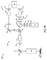
図1Bは、本開示の一実施形態によるシステム100の簡略模式図を示す。図1Bに描かれた光学サブシステム104は、試料103から収集されたDF信号とDIC信号を分離するように配置された鏡面仕上げ瞳マスク134を含む。一実施形態において、図1Cに描かれた鏡面仕上げ瞳マスク134またはピックオフミラーは、鏡面仕上げアニュラス135と、試料103から収集された高NA照明(すなわち、選択された閾値を上回るNAを有する照明)をDF経路111に沿ってDFセンサ112のほうに反射させながら、照明源102からの低NA照明(すなわち、選択された閾値未満のNAを有する照明)を試料103に通過させるように構成された開口部137を含む。別の実施形態において、図示していないが、鏡面仕上げ瞳マスク134またはピックオフミラーは、試料103から収集された低NA照明をDF経路111に沿ってDFセンサ112のほうに反射させながら、照明源102からの高NA照明を試料103に通過させるように働く。これに関連して、鏡面瞳マスク134の照明は、鏡面瞳マスク134の開口部を介して試料103に通過する照明に接近している。
FIG. 1B shows a simplified schematic diagram of the
瞳マスク134に加えて、図1Bの光学サブシステム104は、照明源102からの照明および/または試料103から収集された、散乱または反射された照明を、方向付け、調整および/または選択する任意の個数およびタイプの光学コンポーネントを含んでもよい。
In addition to the
対象の照明は、対物レンズ108に入って試料103を照明する前に、種々の光学素子によって処理されてもよく、その光学素子は、1つ以上の偏光子、1つ以上の波長板、1つ以上のビーム形状コンポーネント、1つ以上のフィルタ、1つ以上の折り畳み式鏡等であるがそれらに限定されない。例えば、図1Bに示すように、照明源102からの照明は、OD120(例えば3位置の)を通って、偏光子122および波長板124(例えば1/4波長板)を通って透過されてもよい。次に、ビームスプリッタ126は、照明源102からの照明の一部を照明経路に沿って方向付けながら、照明の一部を、鏡面仕上げ瞳マスク134を介して通過させてもよい(上記のように)。照明の選択された部分が鏡面仕上げ瞳マスク134を通過した後で、無限焦点レンズ128は選択された照明を、フィルタ130(例えば、405nmフィルタ)を通して透過してもよい。次に、反射鏡132が、フィルタリングされた照明を、対物レンズ108を通って、試料ステージ105上に配置された試料103に方向付けてもよい。一実施形態において、反射鏡132は、試料から収集された望ましくない波長または一組の波長を、付加的な経路(例えばビームダンプへの付加的な経路)に沿って透過させながら、収集信号の光の選択された波長を、特徴付けのための下流のコンポーネントに反射するためのダイクロイックミラーを含む。
The illumination of interest may be processed by various optics before entering the
別の実施形態において、対物レンズ108は、試料103から散乱された照明を収集してDF信号を形成する。次にDF信号は、ミラー132によって反射されて、フィルタ130と無限焦点レンズ128を介して光学経路に沿って戻る方向に方向付けられる。次に、収集された照明は再び鏡面仕上げ瞳マスク134に衝突し、それは、試料からの収集信号をDF成分とDIC成分に分割するように働く。これは、選択されたNA型(例えば低NAまたは高NA)の照明をDF経路111に沿って反射し、残りの照明(例えば高NAまたは低NA)をDIC経路113に透過することによって実行される。例えば、低NA照明が試料103に通された場合、鏡面仕上げ位相マスク134は高NA照明をDF経路111に反射し(また、低NA照明をDIC経路113に透過し)てもよい。別の例として、高NA照明が試料103に通された場合、鏡面仕上げ位相マスク134は低NA照明をDF経路111に反射し(また、高NA照明をDIC経路113に透過し)てもよい。次に、鏡面仕上げ瞳マスク134を介してDF経路111に沿って方向付けられた照明は、レンズ150(例えばチューブレンズ)を介してDFセンサ112(例えば、大型粒子監視に適した一次元センサ)に集束されてもよい。
In another embodiment, the
DF信号の収集と同時に、位相情報を含んだイメージングおよび/または小せん断反射照明が対物レンズ108によって収集され、鏡面瞳マスク134の開口を通過する。次に、DIC信号の成分信号がプリズム138(例えばウォラストンプリズム)またはフィルタのところで互いに干渉する。一実施形態において、システム100はDIC信号を集束するための1つ以上のレンズ136を含む。別の実施形態において、分析器140(例えば切り替え可能な分析器)が、偏光信号におけるノイズ貢献を抑制するために用いられてもよい。次に、ノイズの抑制に続いて、信号は、DIC信号から位相情報を抽出するのに適したDICセンサ114(例えば二次元センサ)にレンズ142(例えばチューブレンズ)を介して集束されてもよい。
Simultaneously with the acquisition of the DF signal, imaging and / or small shear reflection illumination containing phase information is acquired by the
別の実施形態において、コントローラ116は、DFセンサ112から測定されたDF信号を取得し、DICセンサ114から測定されたDIC信号を取得してもよい。別の実施形態において、コントローラ116はデータ融合プロセスを実行してもよく、それにより、DFセンサ112から測定されたDF信号は、DICセンサ114から測定されたDIC信号と融合または合成される。これに関して、コントローラ116は、DF信号の1つ以上の部分をDIC信号の1つ以上の部分と/に合成および/または比較して、試料103の1つ以上の特徴(または欠陥)を特徴付けてもよい。別の実施形態において、コントローラ116は、ユーザインタフェース(図示せず)を介してユーザに、DF信号とDIC信号に関連するイメージデータを表示してもよい。これに関して、ユーザ(またはコントローラ116によって実行されるアルゴリズム)は次に、散乱情報を含むDF信号と、位相情報を含むDIC信号を同時に分析してもよい。
In another embodiment, the
散乱に基づくDF信号と位相に基づくDIC信号の同時の分析は、試料103の欠陥(およびその他の特徴)の検出と分類を充分に増強し得ることに再び注目すべきである。DF信号とDIC信号は、異なる試料と欠陥の特徴に感応することが多いため、これらの信号を融合すると、試料103(および関連する欠陥または特徴)の全体的な理解を増強できる。例えば、スタッキング欠陥の場合、DFに基づく検査プロセスはスタッキング欠陥をポイント欠陥として誤って特徴付けるか、または欠陥を全く検出し損なう。対照的に、DICセンサ114によって測定されたDIC信号は、利用される照明の波長よりも数波長しか高くない欠陥の検出を提供する。照明源102が、200−500nm範囲(例えば405nm)の照明を提供する場合、DICセンサ114は、0.5μm程度に短い特徴に感応する可能性がある。この意味で、DICに基づく検査は、トポグラフィの検査より勝っており、スタッキング欠陥の場合に現れるような試料103上のシャープなエッジの欠陥の良好な識別を提供する。しかしながら、DFに基づく検査は、ポイント欠陥の高品質検出を提供する。DF信号とDIC信号の組み合わせおよび/または比較によって、コントローラ116は所与のセットの欠陥をより容易に且つより正確に検出し特徴付けることができる。例えば、コントローラ116は、DFに基づく特徴とDICに基づく特徴を相関するために、試料103の同じ領域から得られたDF信号とDIC信号を比較して、コントローラ116(またはユーザ)が、所与の領域に現れる1つ以上の欠陥をより正確に特徴付けられるようにする。
It should be noted again that simultaneous analysis of the scattering-based DF signal and the phase-based DIC signal can sufficiently enhance the detection and classification of defects (and other features) in
別の実施形態において、コントローラ116はDFセンサ112からのDF信号と、DICセンサ114からのDIC信号を個別に分析してもよい。これに関連して、システム100がDF信号とDIC信号の検出の光学アーキテクチャを統合するのに対し、コントローラ116は、DF信号とDIC信号を互いに別個に分析するように働く。
In another embodiment, the
本開示を概ね、鏡面仕上げ瞳マスク134を介したDF信号とDIC信号の分離について論じてきたが、本明細書において、そのような構成は本開示への限定ではなく、例示の目的で提供されているに過ぎないことに留意すべきである。DF信号とDIC信号を分離するのに適した任意の光学アーキテクチャが、本開示の文脈で実行され得ることに留意すべきである。
Although the present disclosure has generally discussed the separation of DF and DIC signals via a mirror-finished
図1Dは、本開示の別の実施形態によるシステム100の簡略模式図を示す。本明細書において、図1A−1Cの文脈において説明された種々の構成要素および実施形態は、別途明記しない限り図1Dまで拡張されると解釈されるべきであることに留意すべきである。
FIG. 1D shows a simplified schematic diagram of the
図1Dに描かれた光学サブシステム104は、試料103から収集されたDF信号とDIC信号を分離するように配置された一対の瞳構造158、159を含む。一実施形態において、光学サブシステム104は、収集された照明の第2の部分をDIC経路113に沿って透過しながら、収集された照明の第1の部分をDF経路111に沿って反射させるように構成されたビームスプリッタ154を含む。この配置は限定するものではなく、単に例示として解釈されるべきであることに留意すべきである。例えば、ビームスプリッタ154は、収集された照明の1つの部分をDF経路111に沿って透過しながら、収集された照明の1つの部分をDIC経路113に沿って反射させるように配置されてもよい。
The
一実施形態において、第1の瞳構造158は、選択されたNA閾値未満のNAを有する、DF経路111に沿って伝播される照明を遮断するように働く瞳ブロックを含む。さらに、第2の瞳構造159は、選択されたNA閾値を上回るNAを有する、DIC経路113に沿って伝播される照明を遮断するように働く瞳マスクを含んでもよい。これに関連して、瞳ブロック158と瞳マスク159は互いに接近しており、それにより、一方の構造が、他方の構造によって遮断されるNA型の光を透過する。本明細書において、上記の瞳ブロック158/瞳マスク構成159は限定的でなく、例示のため提供されているに過ぎないことに留意すべきである。例えば、DF経路111が瞳マスクを含み、DIC経路113が瞳ブロックを含んでもよい。これに関連して、DF経路111の瞳マスクは、DF経路111に沿って伝播される、選択されたNA閾値を上回るNAを有する照明を遮断するように働き、DIC経路の瞳ブロックは、DIC経路113に沿って伝播される、選択されたNA閾値未満のNAを有する照明を遮断する。別の実施形態において、光学サブシステム104は、上側のNA範囲を制限する対応する瞳構造がDIC経路113内にない状態で、瞳ブロック158のみを用いてDF信号とDIC信号の分離を実行してもよい。
In one embodiment, the
図1Dの光学サブシステム104は、瞳マスク134に加えて、照明源102からの照明、および/または試料103から収集された散乱または反射された照明を、方向付け、調整および/または選択するための任意の個数およびタイプの光学コンポーネントを含んでもよい。
The
対象の照明は、対物レンズ108に入って試料103を照明する前に種々の光学素子によって処理されてもよく、その光学素子は、1つ以上の偏光子、1つ以上の波長板、1つ以上のビーム形状コンポーネント、1つ以上のフィルタおよび1つ以上の折り畳み式鏡等であるがそれらに限定されない。例えば、図1Dに示すように、照明源102からの照明は、OD120(例えば3位置の)を通って、偏光子122および波長板124(例えば1/4波長板)を通って透過されてもよい。次に、ビームスプリッタ126は、照明源102からの照明の一部を、照明経路に沿って、対物レンズ108を通って試料103に方向付けてもよい。
The illumination of interest may be processed by various optics before entering the
別の実施形態において、対物レンズ108は、試料103から散乱された照明を収集してDF信号を形成する。次にDF信号は、ミラー132によって反射されて、フィルタ130と無限焦点レンズ128を介して光学経路に沿って戻る方向に方向付けられる。次に、収集された照明は再びビームスプリッタ154に衝突し、それは、収集信号を、DF経路111に沿って方向付けられる第1の部分と、DIC経路113に沿って方向付けられる第2の部分に分割するように働く。本明細書で前述したように、瞳構造158、159は、選択されたNA閾値未満および選択されたNA閾値を上回る照明をそれぞれ遮断(または透過)するように働く。DF経路111の場合、低NA光が瞳ブロック158によって遮断された後で、残りの高NA光はレンズ150(例えばチューブレンズ)を介してDFセンサ112(例えば、大型粒子監視に適した一次元センサ)に集束される。DIC経路113の場合、高NA光が瞳マスク159によって遮断された後で、残りの低NA光はレンズ142(例えばチューブレンズ)を介してDICセンサ114(例えば二次元センサ)に集束される。
In another embodiment, the
本開示は、図1A−1Dに描かれる特定の構成とアーキテクチャに限定されず、本明細書において、DF信号がDIC信号から分離され得るいくつかの方式があることが認識される。 The present disclosure is not limited to the particular configuration and architecture depicted in FIGS. 1A-1D, and it is recognized herein that there are several schemes in which the DF signal can be separated from the DIC signal.
いくつかの実施形態において、本明細書に記載される検査システムは、「スタンドアローン」型ツール、または、プロセスツールに物理的に連結されないツールとして構成されてもよい。別の実施形態において、そのような検査システムは、有線および/または無線部分を含み得る伝導媒体によってプロセスツール(図示せず)に連結されてもよい。プロセスツールは、リソグラフィツール、エッチングツール、成膜ツール、研磨ツール、めっきツール、洗浄ツール、またはイオン注入ツール等の当技術分野で知られる任意のプロセスツールを含んでもよい。本明細書に記載されたシステムによって実行される検査の結果は、フィードバック制御技法、フィードフォワード制御技法、および/または現場での制御技法を用いてプロセスまたはプロセスツールのパラメータを変更するために用いられてもよい。プロセスまたはプロセスツールのパラメータは、手動で変えられても自動で変えられてもよい。 In some embodiments, the inspection system described herein may be configured as a "stand-alone" tool, or a tool that is not physically linked to a process tool. In another embodiment, such an inspection system may be connected to a process tool (not shown) by a conductive medium that may include wired and / or wireless portions. The process tool may include any process tool known in the art such as a lithography tool, an etching tool, a film forming tool, a polishing tool, a plating tool, a cleaning tool, or an ion implantation tool. The results of the tests performed by the systems described herein are used to modify the parameters of a process or process tool using feedback control techniques, feedforward control techniques, and / or field control techniques. You may. Process or process tool parameters may be changed manually or automatically.
本明細書に記載された主題は他の構成要素内に含まれた、または他の構成要素に接続された別の構成要素を説明する場合がある。そのような描かれたアーキテクチャは単に例示的なものであり、同じ機能性を達成する多くの別のアーキテクチャが実装され得ることを理解すべきである。概念的な意味で、同じ機能性を達成する構成要素の任意の構成は、望まれる機能性が達成されるように有効に「関連する」。したがって、特定の機能性を達成するために本明細書において組み合わされる任意の2つの構成要素は、アーキテクチャまたは媒介構成要素に拘わらず所望の機能が達成されるように互いに「関連する」と見なされる。同様に、そのように関連付けられた任意の2つの構成要素は、所望の機能性を達成するために互いに「接続」または「連結」されていると見なされ、そのように関連する任意の2つの構成要素は、所望の機能性を達成するために互いに「連結可能」であるとも見なされる。「連結可能」の特定の例は、物理的に嵌合可能および/または物理的に相互作用する構成要素および/または無線相互作用可能および/または無線相互作用する構成要素および/または論理的に相互作用する、および/または論理的に相互作用可能な構成要素を含むがそれらに限定されない。 The subject matter described herein may describe another component that is contained within or is connected to another component. It should be understood that such a drawn architecture is merely exemplary and many different architectures that achieve the same functionality can be implemented. In a conceptual sense, any component of a component that achieves the same functionality is effectively "related" to achieve the desired functionality. Therefore, any two components combined herein to achieve a particular functionality are considered "related" to each other to achieve the desired function, regardless of architecture or intermediary component. .. Similarly, any two components so associated are considered to be "connected" or "connected" to each other to achieve the desired functionality, and any two components so related. The components are also considered to be "connectable" to each other to achieve the desired functionality. Specific examples of "connectable" are physically matable and / or physically interacting components and / or radio interactable and / or radio interacting components and / or logically interacting. Including, but not limited to, acting and / or logically interactable components.
本開示およびその付随する利点は、上記の説明によって理解されるはずであり、また、開示される主題から逸脱せずに、あるいはその重大な利点すべてを犠牲にせずに、構成要素の形状、構成および配置に様々な変更をなしてもよいことは明白である。説明された形式は例示に過ぎず、そのような変更を包含することは、以下の特許請求の範囲の意図である。さらに、本発明は添付の特許請求の範囲によって定義されることを理解すべきである。 The present disclosure and its accompanying advantages should be understood by the above description, and without departing from the disclosed subject matter or at the expense of all of its significant advantages, the shape, composition of the components. And it is clear that various changes may be made to the placement. The format described is only exemplary and it is the intent of the following claims to include such modifications. Furthermore, it should be understood that the present invention is defined by the appended claims.
Claims (24)
1つ以上の照明源と、
試料を固定するように構成された試料ステージと、
第1のセンサと、
第2のセンサと、
光学サブシステムを備え、前記光学サブシステムが、
対物レンズと、
前記対物レンズを介して、前記1つ以上の照明源からの照明を試料の表面に方向付けるように配置された1つ以上の光学素子とを備え、
前記対物レンズは、前記試料の表面から収集信号を収集するように構成され、前記収集信号は、前記試料からの散乱に基づく信号と位相に基づく信号のうち少なくとも1つを含み、
さらに、暗視野信号を暗視野経路に沿って前記第1のセンサに方向付け、微分干渉コントラスト信号を微分干渉コントラスト経路に沿って前記第2のセンサに方向付けることによって、収集信号を暗視野信号と微分干渉コントラスト信号に空間的に分離するように配置された1つ以上の分離光学素子を備え、
前記1つ以上の分離光学素子は、選択されたNA閾値に基づいて、前記収集信号を前記暗視野信号と前記微分干渉コントラスト信号に空間的に分離するように配置された反射型瞳マスクを含む、装置。 A device for simultaneous inspection of darkfield and differential interference contrast contrast.
With one or more lighting sources
A sample stage configured to hold the sample and
The first sensor and
With the second sensor
The optical subsystem is provided with an optical subsystem.
With the objective lens
It comprises one or more optical elements arranged so as to direct illumination from the one or more sources to the surface of the sample through the objective lens.
The objective lens is configured to collect a collected signal from the surface of the sample, the collected signal comprising at least one of a scattering-based signal and a phase-based signal from the sample.
Further, by directing the dark field signal to the first sensor along the dark field path and directing the differential interference contrast signal to the second sensor along the differential interference contrast path, the collected signal is directed to the dark field signal. With one or more separation optical elements arranged to spatially separate into a DIC contrast signal .
The one or more separation optics include a reflective pupil mask arranged to spatially separate the collected signal into the darkfield signal and the differential interference contrast signal based on a selected NA threshold. , Equipment.
前記第1のセンサと前記第2のセンサに通信可能に連結されたコントローラをさらに備え、前記コントローラが、
前記第1のセンサから、前記試料に関連する暗視野信号の1つ以上の測定値を受信し、
前記第2のセンサから、前記試料に関連する微分干渉コントラスト信号の1つ以上の測定値を受信するように構成される、装置。 The device according to claim 1.
Further comprising a controller communicably linked to the first sensor and the second sensor, the controller is:
Receive one or more measurements of the darkfield signal associated with the sample from the first sensor.
An apparatus configured to receive one or more measurements of a differential interference contrast signal associated with the sample from the second sensor.
選択されたNA閾値を上回るNAを有する前記試料からの照明を暗視野経路に沿って反射し、選択されたNA閾値未満のNAを有する前記試料からの照明を、微分干渉経路に沿って透過するように構成されている鏡面仕上げ瞳マスクを含む、装置。 The device according to claim 1, wherein the reflective pupil mask of the optical subsystem is
The illumination from the sample having a NA greater than a selected NA threshold reflected along a dark field path, the illumination from the sample having a NA of less than selected has been NA threshold, transmitted along the differential interference path A device that includes a mirror-finished pupil mask that is configured to.
選択されたNA閾値未満のNAを有する前記試料からの照明を暗視野経路に沿って反射し、選択されたNA閾値を上回るNAを有する前記試料からの照明を、微分干渉コントラスト経路に沿って透過するように構成されている鏡面仕上げ瞳マスクを含む、装置。 The device according to claim 1, wherein the reflective pupil mask of the optical subsystem is
The illumination from the sample having a NA of less than a selected NA threshold reflected along a dark field path, the illumination from the sample having a NA in excess of NA threshold is selected, along differential interference contrast path A device that includes a mirror-finished pupil mask that is configured to be transparent.
収集信号を、前記暗視野経路に沿って前記第1のセンサに方向付けられる第1の部分と、前記微分干渉コントラスト経路に沿って前記第2のセンサに方向付けられる第2の部分とに分離するように構成されたビームスプリッタを備えている、装置。 The apparatus according to claim 1, wherein the one or more separation optical elements of the optical subsystem are
The collected signal is split into a first portion directed to the first sensor along the darkfield path and a second portion directed to the second sensor along the differential interference contrast path. A device with a beam splitter configured to do so.
1つ以上の照明源と、
試料を固定するように構成された試料ステージと、
光学サブシステムを備え、前記光学サブシステムが、
対物レンズと、
選択されたNA閾値未満のNAを有する照明を透過させるように構成された鏡面仕上げ瞳マスクと、
前記鏡面仕上げ瞳マスクを介して、選択されたNA閾値未満のNAを有する照明を方向付けるように配置された1つ以上の光学素子とを備え、
前記1つ以上の光学素子はさらに、前記鏡面仕上げ瞳マスクを介して透過された照明を、前記対物レンズを通過させて前記試料の表面に方向付けるように構成され、
前記対物レンズは、前記試料の表面から収集信号を収集するように構成され、前記収集信号は、前記試料からの散乱信号と位相信号のうち少なくとも1つを含み、
前記鏡面仕上げ瞳マスクはさらに、選択されたNA閾値を上回るNAを有する収集された照明の部分を暗視野経路に沿って第1のセンサに反射し、選択されたNA閾値未満のNAを有する、収集された照明の一部を、微分干渉コントラスト経路に沿って第2のセンサに透過させることによって、前記収集信号を暗視野信号と微分干渉コントラスト信号に空間的に分離するように構成されている装置。 A device for simultaneous inspection of darkfield and differential interference contrast contrast.
With one or more lighting sources
A sample stage configured to hold the sample and
The optical subsystem is provided with an optical subsystem.
With the objective lens
A mirror-finished pupil mask configured to transmit illumination with an NA below the selected NA threshold, and
Includes one or more optics arranged to direct illumination with NA below the selected NA threshold through the mirror-finished pupil mask.
The one or more optical elements are further configured to direct the illumination transmitted through the mirror-finished pupil mask through the objective lens to the surface of the sample.
The objective lens is configured to collect a collected signal from the surface of the sample, the collected signal including at least one of a scattered signal and a phase signal from the sample.
The mirror-finished pupil mask further reflects a portion of the collected illumination having an NA above the selected NA threshold to the first sensor along the darkfield path and has an NA below the selected NA threshold. A part of the collected illumination is transmitted to the second sensor along the differential interference contrast contrast path, so that the collected signal is spatially separated into a dark field signal and a differential interference contrast contrast signal. apparatus.
1つ以上の照明源と、
試料を固定するように構成された試料ステージと、
光学サブシステムを備え、前記光学サブシステムが、
対物レンズと、
前記対物レンズを介して、照明を試料の表面に方向付けるように配置された1つ以上の光学素子とを備え、前記対物レンズは、前記試料の表面からの収集信号を収集するように構成され、前記収集信号は、前記試料からの散乱信号と位相信号のうち少なくとも1つを含み、
さらに、収集された照明の第1の部分を暗視野経路に沿って方向付けるように構成されたビームスプリッタを備え、前記ビームスプリッタはさらに、収集された照明の第2の部分を微分干渉コントラスト経路に沿って透過するように構成され、
さらに、前記暗視野経路に沿って配置され、選択されたNA閾値未満のNAを有する照明を遮断するように構成された瞳ブロックと、
微分干渉コントラスト経路に沿って配置され、選択されたNA閾値を上回るNAを有する照明を遮断するように構成された瞳マスクとを備え、
前記暗視野経路の瞳ブロックによって透過された照明を収集するように構成された第1のセンサと、
微分干渉コントラスト経路の瞳マスクによって透過された照明を収集するように構成された第2のセンサを備える装置。 A device for simultaneous inspection of darkfield and differential interference contrast contrast.
With one or more lighting sources
A sample stage configured to hold the sample and
The optical subsystem is provided with an optical subsystem.
With the objective lens
The objective lens comprises one or more optical elements arranged to direct illumination to the surface of the sample via the objective lens, the objective lens being configured to collect a collection signal from the surface of the sample. , The collected signal includes at least one of a scattered signal and a phase signal from the sample.
In addition, the beam splitter is configured to direct a first portion of the collected illumination along a darkfield path, which further directs a second portion of the collected illumination into a differential interference contrast path. It is configured to be transparent along
Further, a pupil block arranged along the dark field path and configured to block illumination having an NA below the selected NA threshold.
They are arranged along a differential interference Contrast route, and a configuration pupil mask to block the illumination having an NA greater than the NA threshold selected,
A first sensor configured to collect the illumination transmitted by the pupil block in the darkfield path, and
A device comprising a second sensor configured to collect the illumination transmitted by the pupil mask of the differential interference contrast path.
Applications Claiming Priority (5)
| Application Number | Priority Date | Filing Date | Title |
|---|---|---|---|
| US201462027393P | 2014-07-22 | 2014-07-22 | |
| US62/027,393 | 2014-07-22 | ||
| US14/804,296 | 2015-07-20 | ||
| US14/804,296 US9726615B2 (en) | 2014-07-22 | 2015-07-20 | System and method for simultaneous dark field and phase contrast inspection |
| PCT/US2015/041409 WO2016014590A1 (en) | 2014-07-22 | 2015-07-21 | System and method for simultaneous dark field and phase contrast inspection |
Publications (3)
| Publication Number | Publication Date |
|---|---|
| JP2017531162A JP2017531162A (en) | 2017-10-19 |
| JP2017531162A5 JP2017531162A5 (en) | 2018-08-30 |
| JP6807829B2 true JP6807829B2 (en) | 2021-01-06 |
Family
ID=55163659
Family Applications (1)
| Application Number | Title | Priority Date | Filing Date |
|---|---|---|---|
| JP2017503491A Active JP6807829B2 (en) | 2014-07-22 | 2015-07-21 | Systems and methods for simultaneous darkfield and phase contrast inspection |
Country Status (8)
| Country | Link |
|---|---|
| US (1) | US9726615B2 (en) |
| JP (1) | JP6807829B2 (en) |
| KR (1) | KR102241899B1 (en) |
| CN (1) | CN106575631B (en) |
| DE (1) | DE112015003394B4 (en) |
| SG (1) | SG11201610820YA (en) |
| TW (1) | TWI639822B (en) |
| WO (1) | WO2016014590A1 (en) |
Families Citing this family (10)
| Publication number | Priority date | Publication date | Assignee | Title |
|---|---|---|---|---|
| US9726615B2 (en) | 2014-07-22 | 2017-08-08 | Kla-Tencor Corporation | System and method for simultaneous dark field and phase contrast inspection |
| TWI606101B (en) | 2016-12-28 | 2017-11-21 | 財團法人工業技術研究院 | Coating composition and method of manufacturing the same |
| US10422984B2 (en) * | 2017-05-12 | 2019-09-24 | Applied Materials, Inc. | Flexible mode scanning optical microscopy and inspection system |
| CN108022849B (en) * | 2017-11-30 | 2020-06-16 | 上海华力微电子有限公司 | Method and system for automatically optimizing light intensity condition of bright field defect detection equipment |
| US10845187B2 (en) * | 2018-03-02 | 2020-11-24 | Drexel University | Multiscale deformation measurements leveraging tailorable and multispectral speckle patterns |
| US11067389B2 (en) * | 2018-03-13 | 2021-07-20 | Kla Corporation | Overlay metrology system and method |
| US10732130B2 (en) * | 2018-06-19 | 2020-08-04 | Kla-Tencor Corporation | Embedded particle depth binning based on multiple scattering signals |
| US11017520B2 (en) * | 2018-09-04 | 2021-05-25 | Kla Corporation | Multi-wavelength interferometry for defect classification |
| US10705026B2 (en) * | 2018-10-26 | 2020-07-07 | Kla Corporation | Scanning differential interference contrast in an imaging system design |
| WO2023286220A1 (en) * | 2021-07-14 | 2023-01-19 | 株式会社日立ハイテク | Defect inspection device |
Family Cites Families (25)
| Publication number | Priority date | Publication date | Assignee | Title |
|---|---|---|---|---|
| JPS5961142A (en) * | 1982-09-30 | 1984-04-07 | Fujitsu Ltd | Inspecting device of defect |
| US5798829A (en) | 1996-03-05 | 1998-08-25 | Kla-Tencor Corporation | Single laser bright field and dark field system for detecting anomalies of a sample |
| US6999183B2 (en) | 1998-11-18 | 2006-02-14 | Kla-Tencor Corporation | Detection system for nanometer scale topographic measurements of reflective surfaces |
| US6809808B2 (en) * | 2002-03-22 | 2004-10-26 | Applied Materials, Inc. | Wafer defect detection system with traveling lens multi-beam scanner |
| US20030215791A1 (en) | 2002-05-20 | 2003-11-20 | Applied Spectral Imaging Ltd. | Method of and system for multiplexed analysis by spectral imaging |
| JP3878107B2 (en) * | 2002-11-06 | 2007-02-07 | 株式会社日立ハイテクノロジーズ | Defect inspection method and apparatus |
| US7957066B2 (en) * | 2003-02-21 | 2011-06-07 | Kla-Tencor Corporation | Split field inspection system using small catadioptric objectives |
| US20050254065A1 (en) * | 2004-05-12 | 2005-11-17 | Stokowski Stanley E | Method and apparatus for detecting surface characteristics on a mask blank |
| US7924434B2 (en) * | 2005-08-02 | 2011-04-12 | Kla-Tencor Technologies Corp. | Systems configured to generate output corresponding to defects on a specimen |
| US7345754B1 (en) | 2005-09-16 | 2008-03-18 | Kla-Tencor Technologies Corp. | Fourier filters and wafer inspection systems |
| WO2008048612A2 (en) | 2006-10-17 | 2008-04-24 | Hnuphotonics | Miniature microscope camera |
| US7728969B2 (en) | 2006-12-05 | 2010-06-01 | Kla-Tencor Technologies Corp. | Methods and systems for identifying defect types on a wafer |
| JP2008151865A (en) | 2006-12-14 | 2008-07-03 | Olympus Corp | Microscope system |
| DE102007047935A1 (en) | 2007-03-19 | 2008-09-25 | Vistec Semiconductor Systems Gmbh | Apparatus and method for inspection of defects at the edge region of a wafer and use of the device in a wafer inspection device |
| US7782452B2 (en) | 2007-08-31 | 2010-08-24 | Kla-Tencor Technologies Corp. | Systems and method for simultaneously inspecting a specimen with two distinct channels |
| JP5104346B2 (en) * | 2008-01-29 | 2012-12-19 | 株式会社ニコン | Surface defect inspection method and apparatus |
| US20120225475A1 (en) | 2010-11-16 | 2012-09-06 | 1087 Systems, Inc. | Cytometry system with quantum cascade laser source, acoustic detector, and micro-fluidic cell handling system configured for inspection of individual cells |
| US10048480B2 (en) | 2011-01-07 | 2018-08-14 | Zeta Instruments, Inc. | 3D microscope including insertable components to provide multiple imaging and measurement capabilities |
| US9279774B2 (en) | 2011-07-12 | 2016-03-08 | Kla-Tencor Corp. | Wafer inspection |
| AU2012288992B2 (en) * | 2011-07-28 | 2015-03-12 | Paul Scherrer Institut | Method for image fusion based on principal component analysis |
| US8755044B2 (en) | 2011-08-15 | 2014-06-17 | Kla-Tencor Corporation | Large particle detection for multi-spot surface scanning inspection systems |
| KR102117133B1 (en) | 2012-03-07 | 2020-05-29 | 케이엘에이 코포레이션 | Wafer and reticle inspection systems and method for selecting illumination pupil configurations |
| US9053390B2 (en) | 2012-08-14 | 2015-06-09 | Kla-Tencor Corporation | Automated inspection scenario generation |
| JP6124774B2 (en) * | 2013-03-22 | 2017-05-10 | オリンパス株式会社 | Phase distribution measuring method and phase distribution measuring apparatus |
| US9726615B2 (en) | 2014-07-22 | 2017-08-08 | Kla-Tencor Corporation | System and method for simultaneous dark field and phase contrast inspection |
-
2015
- 2015-07-20 US US14/804,296 patent/US9726615B2/en active Active
- 2015-07-21 WO PCT/US2015/041409 patent/WO2016014590A1/en active Application Filing
- 2015-07-21 JP JP2017503491A patent/JP6807829B2/en active Active
- 2015-07-21 DE DE112015003394.7T patent/DE112015003394B4/en active Active
- 2015-07-21 SG SG11201610820YA patent/SG11201610820YA/en unknown
- 2015-07-21 CN CN201580038195.1A patent/CN106575631B/en active Active
- 2015-07-21 KR KR1020177004868A patent/KR102241899B1/en active IP Right Grant
- 2015-07-22 TW TW104123748A patent/TWI639822B/en active
Also Published As
| Publication number | Publication date |
|---|---|
| SG11201610820YA (en) | 2017-02-27 |
| TW201617603A (en) | 2016-05-16 |
| CN106575631A (en) | 2017-04-19 |
| US20160025645A1 (en) | 2016-01-28 |
| JP2017531162A (en) | 2017-10-19 |
| CN106575631B (en) | 2019-02-01 |
| KR102241899B1 (en) | 2021-04-16 |
| KR20170033884A (en) | 2017-03-27 |
| DE112015003394T5 (en) | 2017-03-30 |
| US9726615B2 (en) | 2017-08-08 |
| TWI639822B (en) | 2018-11-01 |
| WO2016014590A1 (en) | 2016-01-28 |
| DE112015003394B4 (en) | 2023-04-27 |
Similar Documents
| Publication | Publication Date | Title |
|---|---|---|
| JP6807829B2 (en) | Systems and methods for simultaneous darkfield and phase contrast inspection | |
| US10422984B2 (en) | Flexible mode scanning optical microscopy and inspection system | |
| JP6755323B2 (en) | Methods and equipment for polarized wafer inspection | |
| JP6231156B2 (en) | System and method for detecting defects on a wafer | |
| KR102367236B1 (en) | Method and Apparatus for Suppression of Spots in Laser Dark Field Systems | |
| TWI615608B (en) | Method, system, and computer-readable medium for detecting defects on a wafer | |
| KR102318273B1 (en) | Inspection systems and techniques with enhanced detection | |
| US11366069B2 (en) | Simultaneous multi-directional laser wafer inspection | |
| JP2007511739A5 (en) | ||
| US9239295B2 (en) | Variable polarization wafer inspection | |
| TW201506383A (en) | Apparatus and methods for finding a best aperture and mode to enhance defect detection | |
| TW201245896A (en) | Structured illumination for contrast enhancement in overlay metrology | |
| WO2005024404B1 (en) | Methods and systems for inspection of a specimen using different inspection parameters | |
| JP2022509599A (en) | Radial polarizing element for particle detection | |
| KR102213732B1 (en) | Inspection system including parallel imaging paths with multiple and selectable spectral bands | |
| JPH1090192A (en) | Optical inspection of specimen using multi-channel response from the specimen | |
| KR101731498B1 (en) | Apparatus and method for inspecting display surface | |
| CN109991238A (en) | Defect detecting device and method |
Legal Events
| Date | Code | Title | Description |
|---|---|---|---|
| A521 | Request for written amendment filed |
Free format text: JAPANESE INTERMEDIATE CODE: A523 Effective date: 20180719 |
|
| A621 | Written request for application examination |
Free format text: JAPANESE INTERMEDIATE CODE: A621 Effective date: 20180719 |
|
| A977 | Report on retrieval |
Free format text: JAPANESE INTERMEDIATE CODE: A971007 Effective date: 20190417 |
|
| A131 | Notification of reasons for refusal |
Free format text: JAPANESE INTERMEDIATE CODE: A131 Effective date: 20190423 |
|
| A521 | Request for written amendment filed |
Free format text: JAPANESE INTERMEDIATE CODE: A523 Effective date: 20190718 |
|
| A131 | Notification of reasons for refusal |
Free format text: JAPANESE INTERMEDIATE CODE: A131 Effective date: 20200107 |
|
| A601 | Written request for extension of time |
Free format text: JAPANESE INTERMEDIATE CODE: A601 Effective date: 20200402 |
|
| A521 | Request for written amendment filed |
Free format text: JAPANESE INTERMEDIATE CODE: A523 Effective date: 20200603 |
|
| TRDD | Decision of grant or rejection written | ||
| A01 | Written decision to grant a patent or to grant a registration (utility model) |
Free format text: JAPANESE INTERMEDIATE CODE: A01 Effective date: 20201117 |
|
| A61 | First payment of annual fees (during grant procedure) |
Free format text: JAPANESE INTERMEDIATE CODE: A61 Effective date: 20201208 |
|
| R150 | Certificate of patent or registration of utility model |
Ref document number: 6807829 Country of ref document: JP Free format text: JAPANESE INTERMEDIATE CODE: R150 |
|
| R250 | Receipt of annual fees |
Free format text: JAPANESE INTERMEDIATE CODE: R250 |