JP6799985B2 - Distance measuring device - Google Patents
Distance measuring device Download PDFInfo
- Publication number
- JP6799985B2 JP6799985B2 JP2016189547A JP2016189547A JP6799985B2 JP 6799985 B2 JP6799985 B2 JP 6799985B2 JP 2016189547 A JP2016189547 A JP 2016189547A JP 2016189547 A JP2016189547 A JP 2016189547A JP 6799985 B2 JP6799985 B2 JP 6799985B2
- Authority
- JP
- Japan
- Prior art keywords
- circuit
- light emitting
- less
- wiring
- emitting element
- Prior art date
- Legal status (The legal status is an assumption and is not a legal conclusion. Google has not performed a legal analysis and makes no representation as to the accuracy of the status listed.)
- Active
Links
Images


Classifications
-
- G—PHYSICS
- G01—MEASURING; TESTING
- G01S—RADIO DIRECTION-FINDING; RADIO NAVIGATION; DETERMINING DISTANCE OR VELOCITY BY USE OF RADIO WAVES; LOCATING OR PRESENCE-DETECTING BY USE OF THE REFLECTION OR RERADIATION OF RADIO WAVES; ANALOGOUS ARRANGEMENTS USING OTHER WAVES
- G01S7/00—Details of systems according to groups G01S13/00, G01S15/00, G01S17/00
- G01S7/48—Details of systems according to groups G01S13/00, G01S15/00, G01S17/00 of systems according to group G01S17/00
- G01S7/483—Details of pulse systems
- G01S7/484—Transmitters
-
- G—PHYSICS
- G01—MEASURING; TESTING
- G01S—RADIO DIRECTION-FINDING; RADIO NAVIGATION; DETERMINING DISTANCE OR VELOCITY BY USE OF RADIO WAVES; LOCATING OR PRESENCE-DETECTING BY USE OF THE REFLECTION OR RERADIATION OF RADIO WAVES; ANALOGOUS ARRANGEMENTS USING OTHER WAVES
- G01S17/00—Systems using the reflection or reradiation of electromagnetic waves other than radio waves, e.g. lidar systems
- G01S17/02—Systems using the reflection of electromagnetic waves other than radio waves
- G01S17/06—Systems determining position data of a target
- G01S17/08—Systems determining position data of a target for measuring distance only
- G01S17/10—Systems determining position data of a target for measuring distance only using transmission of interrupted, pulse-modulated waves
Description
本発明は、パルス光の発光回路に関する。 The present invention relates to a pulsed light emitting circuit.
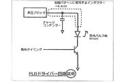
パルス光を用いた測距装置が知られている。図1の回路は、パルス測距を行う為の発光部回路である(特許文献1参照)。この種の回路では、従来10nS程度のパルス幅で発光していた。この場合、本体の不要な内部反射によりレーザの干渉が起こり易く、測距値の偏差が悪化する。この為、本体に干渉を回避させる為の光学機構を設ける必要が有り、この事が本体のコストUPや小型化の妨げになっていた。 A ranging device using pulsed light is known. The circuit of FIG. 1 is a light emitting unit circuit for performing pulse ranging (see Patent Document 1). In this type of circuit, light is emitted with a pulse width of about 10 nS in the past. In this case, laser interference is likely to occur due to unnecessary internal reflection of the main body, and the deviation of the distance measurement value is exacerbated. For this reason, it is necessary to provide an optical mechanism in the main body to avoid interference, which hinders the cost increase and miniaturization of the main body.
他方で、2nS以下のパルス幅で光らせる事で、レーザの干渉性を抑える事が出来、レーザ干渉回避用の光学機構を設けなくても高い精度の測距が可能となる。この場合、測距精度を確保しつつ、本体小型化や部品削減による安価な製品構成が実現可能となる(特許文献2参照)。 On the other hand, by illuminating with a pulse width of 2 nS or less, the coherence of the laser can be suppressed, and high-precision distance measurement is possible without providing an optical mechanism for avoiding laser interference. In this case, it is possible to realize an inexpensive product configuration by downsizing the main body and reducing parts while ensuring the distance measurement accuracy (see Patent Document 2).
図1の回路で2nSのパルス光を発光させる場合、回路の配線パターンのインダクタンスの影響で周波数特性が悪化し、2nS以下でパスル発光が出来なかった。本発明は、パルス幅が2nS以下のパルス光の発光を行う技術の提供を目的とする。 When the circuit of FIG. 1 emits 2 nS pulsed light, the frequency characteristics deteriorate due to the influence of the inductance of the wiring pattern of the circuit, and the pulse light cannot be emitted at 2 nS or less. An object of the present invention is to provide a technique for emitting pulsed light having a pulse width of 2 nS or less.
請求項1に記載の発明は、パルス光を発光する回路であって、電圧発生回路と、発光素子と、前記電圧発生回路と前記発光素子を接続する回路配線と、前記回路配線に一端が接続されたチャージコンデンサと、前記発光素子への電圧印加のON/OFFを決定するスイッチング素子とを備え、前記回路配線は、パターン長(L)、パターン幅(W)、パターン厚(H)および1.4nH以下のインダクタンス成分を有することで前記発光素子からのパルス光のパルス幅2nsにおける減衰値を3dB以下としたPCB配線であり、そのインダクタンス成分は下記数1により計算され、前記発光素子は、2ns以下のパルス幅のパルス光を発光し、前記Lは3mm以下、前記Wは1mm以上、前記Hは18μm以上であることを特徴とする発光回路である。

本発明によれば、パルス幅が2nS以下のパルス光の発光を行う技術が得られる。 According to the present invention, a technique for emitting pulsed light having a pulse width of 2 nS or less can be obtained.
(構成)
図2には、発明を利用した発光回路100が示されている。発光回路100は、電源となる昇圧ブロック101、チャージコンデンサ102、発光素子であるレーザダイオード103、スイッチング素子104を備えている。昇圧ブロック101から電圧を与え、チャージコンデンサ102に電荷を蓄積した状態で、スイッチング素子104をONにすると、チャージコンデンサ102に蓄積された電荷がレーザダイオード103に一瞬流れ、レーザダイオード103がパルス発光する。
(Constitution)
FIG. 2 shows a
この際、レーザダイオード103に至る配線105のインダクタンスが発光パルス幅に大きく影響する。図3には、配線105のインダクタンスの違いによる周波数(パルス幅に対応)と減衰値の関係が示されている。図3から明らかなように、配線105のインダクタンスを1.4nH以下とすることで、パルス幅2nSにおける減衰値を3dBに抑えられ、2nS発光を実現できる。
At this time, the inductance of the
以下、配線105のインダクタンスを1.4nH以下とする具体例について説明する。一般に、PCB配線パターンに対するインダクタンス成分(μH)は概略以下の式で求められる。なお、L:パターン長、W:パターン幅、H:パターン厚である。
Hereinafter, a specific example in which the inductance of the
![]()
![]()
従来の場合のパターンは、L=7mm、W=1mm、H=18μm程度であり、配線105のインダクタンスは、4.4nH程度であった。本実施形態では、配線105をW=1mm、H=18μmとした為、インダクタンスを1.4nH以下とするには、L=3mm以下とすればよいことが判る。
The pattern in the conventional case was about L = 7 mm, W = 1 mm, and H = 18 μm, and the inductance of the
以上述べたように、発光回路100は、パルス光を発光する回路であって、電圧発生回路である昇圧ブロック101と、発光素子であるレーザダイオード103と、回路配線105と、回路配線105に一端が接続されたチャージコンデンサ102と、レーザダイオード103への電圧印加のON/OFFを決定するスイッチング素子104とを備え、回路配線105のインダクタンスは、1.4nH以下であり、レーザダイオード103は、2nS以下のパルス幅のパルス光を発光することを特徴とする。回路配線105のインダクタンスを1.4nH以下とすることで、レーザダイオード103が2nS以下パルス幅のパルス光を発光する際に、減衰値を3dB以下に抑えることができる。つまり2nS以下のパルス発光を実現できる。
As described above, the
Claims (1)
電圧発生回路と、
発光素子と、
前記電圧発生回路と前記発光素子を接続する回路配線と、
前記回路配線に一端が接続されたチャージコンデンサと、
前記発光素子への電圧印加のON/OFFを決定するスイッチング素子と
を備え、
前記回路配線は、パターン長(L)、パターン幅(W)、パターン厚(H)および1.4nH以下のインダクタンス成分を有することで前記発光素子からのパルス光のパルス幅2nsにおける減衰値を3dB以下としたPCB配線であり、そのインダクタンス成分は下記数1により計算され、
前記発光素子は、2ns以下のパルス幅のパルス光を発光し、
前記Lは2.5mm以下、前記Wは0.5mm以上、前記Hは18μm以上であることを特徴とする発光回路。
Voltage generation circuit and
Light emitting element and
The circuit wiring that connects the voltage generation circuit and the light emitting element,
A charge capacitor with one end connected to the circuit wiring,
A switching element for determining ON / OFF of voltage application to the light emitting element is provided.
The circuit wiring has a pattern length (L), a pattern width (W), a pattern thickness (H), and an inductance component of 1.4 nH or less, so that the attenuation value of the pulsed light from the light emitting element in the pulse width of 2 ns is 3 dB. The PCB wiring is as follows, and its inductance component is calculated by the following equation 1.
The light emitting element emits pulsed light having a pulse width of 2 ns or less .
A light emitting circuit characterized in that L is 2.5 mm or less, W is 0.5 mm or more, and H is 18 μm or more .
Priority Applications (4)
| Application Number | Priority Date | Filing Date | Title |
|---|---|---|---|
| JP2016189547A JP6799985B2 (en) | 2016-09-28 | 2016-09-28 | Distance measuring device |
| EP17189542.8A EP3301473B1 (en) | 2016-09-28 | 2017-09-06 | Distance measuring device |
| US15/711,299 US20180088213A1 (en) | 2016-09-28 | 2017-09-21 | Distance measuring device |
| US16/369,670 US20190227171A1 (en) | 2016-09-28 | 2019-03-29 | Distance measuring device |
Applications Claiming Priority (1)
| Application Number | Priority Date | Filing Date | Title |
|---|---|---|---|
| JP2016189547A JP6799985B2 (en) | 2016-09-28 | 2016-09-28 | Distance measuring device |
Publications (3)
| Publication Number | Publication Date |
|---|---|
| JP2018054415A JP2018054415A (en) | 2018-04-05 |
| JP2018054415A5 JP2018054415A5 (en) | 2019-07-18 |
| JP6799985B2 true JP6799985B2 (en) | 2020-12-16 |
Family
ID=59811102
Family Applications (1)
| Application Number | Title | Priority Date | Filing Date |
|---|---|---|---|
| JP2016189547A Active JP6799985B2 (en) | 2016-09-28 | 2016-09-28 | Distance measuring device |
Country Status (3)
| Country | Link |
|---|---|
| US (1) | US20180088213A1 (en) |
| EP (1) | EP3301473B1 (en) |
| JP (1) | JP6799985B2 (en) |
Families Citing this family (10)
| Publication number | Priority date | Publication date | Assignee | Title |
|---|---|---|---|---|
| CN112005455A (en) * | 2018-04-19 | 2020-11-27 | 索尼半导体解决方案公司 | Semiconductor laser driving device and method for manufacturing the same |
| EP3912432A1 (en) * | 2019-01-14 | 2021-11-24 | Lumileds Holding B.V. | Lighting device for frequency-modulated emission |
| EP3980797A1 (en) | 2019-07-25 | 2022-04-13 | Quantum Technologies UG (Haftungsbeschränkt) | Device and method for using diamond nanocrystals having nv colour centres in cmos circuits |
| WO2021065096A1 (en) * | 2019-09-30 | 2021-04-08 | 株式会社村田製作所 | Laser diode drive circuit |
| JP7318718B2 (en) * | 2019-09-30 | 2023-08-01 | 株式会社村田製作所 | laser diode drive circuit |
| DE102020114782A1 (en) | 2020-01-07 | 2021-07-08 | Elmos Semiconductor Se | Mechanic-free LIDAR system for a drone |
| WO2021140160A1 (en) | 2020-01-07 | 2021-07-15 | Elmos Semiconductor Se | Light module and lidar apparatus having at least one light module of this type |
| DE102020124564A1 (en) | 2020-01-07 | 2021-07-08 | Elmos Semiconductor Se | Lens for a mechanically-free LIDAR system for a drone |
| DE102021101584B3 (en) | 2021-01-25 | 2022-03-10 | Elmos Semiconductor Se | Mechanic-less ISO26262 compliant LIDAR system |
| DE102021128923A1 (en) | 2021-01-25 | 2022-07-28 | Elmos Semiconductor Se | Mechanic-less ISO26262 compliant LIDAR system |
Family Cites Families (8)
| Publication number | Priority date | Publication date | Assignee | Title |
|---|---|---|---|---|
| DE3540157A1 (en) * | 1985-11-13 | 1987-05-21 | Messerschmitt Boelkow Blohm | METHOD AND DEVICE FOR DISTANCE MEASUREMENT |
| DE4316348A1 (en) * | 1993-05-15 | 1994-11-17 | Wild Heerbrugg Ag | Distance measuring device |
| JP3529718B2 (en) * | 2000-10-03 | 2004-05-24 | ローム株式会社 | Light emitting device of portable telephone and driving IC therefor |
| JP4954725B2 (en) * | 2007-01-23 | 2012-06-20 | 三菱電機株式会社 | LIGHT EMITTING ELEMENT DRIVE DEVICE AND DISPLAY DEVICE USING THE SAME |
| JP5222117B2 (en) * | 2008-12-10 | 2013-06-26 | ヤマハ発動機株式会社 | Laser light generation circuit, laser radar device, and transportation equipment |
| GB2492833A (en) * | 2011-07-14 | 2013-01-16 | Softkinetic Sensors Nv | LED boost converter driver circuit for Time Of Flight light sources |
| US9368936B1 (en) * | 2013-09-30 | 2016-06-14 | Google Inc. | Laser diode firing system |
| JP6651123B2 (en) * | 2015-01-08 | 2020-02-19 | 株式会社リコー | Light source driving device, light source device, distance measuring device, moving body device, laser beam machine, and light source driving method |
-
2016
- 2016-09-28 JP JP2016189547A patent/JP6799985B2/en active Active
-
2017
- 2017-09-06 EP EP17189542.8A patent/EP3301473B1/en active Active
- 2017-09-21 US US15/711,299 patent/US20180088213A1/en not_active Abandoned
Also Published As
| Publication number | Publication date |
|---|---|
| JP2018054415A (en) | 2018-04-05 |
| EP3301473A1 (en) | 2018-04-04 |
| EP3301473B1 (en) | 2021-08-25 |
| US20180088213A1 (en) | 2018-03-29 |
Similar Documents
| Publication | Publication Date | Title |
|---|---|---|
| JP6799985B2 (en) | Distance measuring device | |
| JP6569236B2 (en) | Laser diode drive circuit and laser radar device | |
| US10989813B2 (en) | Distance measurement apparatus | |
| WO2015119979A3 (en) | Vcsel array for a depth camera | |
| JP5608038B2 (en) | Filter circuit and lighting apparatus using the same | |
| FR3092160B1 (en) | vehicle lamp | |
| EP1978377A3 (en) | Distance/speed meter and distance/speed measuring method | |
| US9295138B2 (en) | Lighting device and luminaire using the same | |
| JP2015197669A5 (en) | ||
| JP4863196B2 (en) | Lighting control circuit for flash discharge tube | |
| US10868522B2 (en) | Square pulse optical transmission circuit | |
| US8901826B2 (en) | Light sensing module and calibration method for driving current of light source | |
| JP5297034B2 (en) | Light measuring device | |
| JP2015165196A (en) | Distance measuring device, mobile body, and distance measuring method | |
| TW200516766A (en) | A laser diode driving circuit and an optical head | |
| JP2017130749A5 (en) | ||
| JP2018040774A (en) | Ranging device | |
| JP6433049B2 (en) | Carrier type strain measuring device | |
| UA46427S (en) | 1. ELEMENT OF THE CONTROLLER HOUSING FOR AN ELECTRONIC DEVICE | |
| RU2016101849A (en) | EXTENDED LIGHTING UNIT FOR VEHICLE, EXTENDED LIGHTING UNIT AND METHOD FOR FORMING EXTENDED LIGHTING UNIT | |
| JP2021025778A (en) | Laser driving device, method for adjusting pulse width, and sensing module | |
| JP2017017196A5 (en) | ||
| JP2016154414A (en) | Power source unit, lighting device and head lamp unit for vehicle | |
| JP2023034439A (en) | Laser emission device and optical distance measuring device | |
| JP2015165195A (en) | Distance measuring device, mobile body, and distance measuring method |
Legal Events
| Date | Code | Title | Description |
|---|---|---|---|
| A521 | Request for written amendment filed |
Free format text: JAPANESE INTERMEDIATE CODE: A523 Effective date: 20170911 |
|
| A521 | Request for written amendment filed |
Free format text: JAPANESE INTERMEDIATE CODE: A523 Effective date: 20190612 |
|
| A621 | Written request for application examination |
Free format text: JAPANESE INTERMEDIATE CODE: A621 Effective date: 20190827 |
|
| A977 | Report on retrieval |
Free format text: JAPANESE INTERMEDIATE CODE: A971007 Effective date: 20200727 |
|
| A131 | Notification of reasons for refusal |
Free format text: JAPANESE INTERMEDIATE CODE: A131 Effective date: 20200818 |
|
| A521 | Request for written amendment filed |
Free format text: JAPANESE INTERMEDIATE CODE: A523 Effective date: 20201007 |
|
| TRDD | Decision of grant or rejection written | ||
| A01 | Written decision to grant a patent or to grant a registration (utility model) |
Free format text: JAPANESE INTERMEDIATE CODE: A01 Effective date: 20201113 |
|
| A61 | First payment of annual fees (during grant procedure) |
Free format text: JAPANESE INTERMEDIATE CODE: A61 Effective date: 20201124 |
|
| R150 | Certificate of patent or registration of utility model |
Ref document number: 6799985 Country of ref document: JP Free format text: JAPANESE INTERMEDIATE CODE: R150 |
|
| R250 | Receipt of annual fees |
Free format text: JAPANESE INTERMEDIATE CODE: R250 |