JP6789675B2 - Semiconductor light emitting device and its manufacturing method - Google Patents

Semiconductor light emitting device and its manufacturing method Download PDF

Info

Publication number
JP6789675B2
JP6789675B2 JP2016111145A JP2016111145A JP6789675B2 JP 6789675 B2 JP6789675 B2 JP 6789675B2 JP 2016111145 A JP2016111145 A JP 2016111145A JP 2016111145 A JP2016111145 A JP 2016111145A JP 6789675 B2 JP6789675 B2 JP 6789675B2
Authority
JP
Japan
Prior art keywords
layer
light emitting
substrate
modified layer
emitting device
Prior art date
Legal status (The legal status is an assumption and is not a legal conclusion. Google has not performed a legal analysis and makes no representation as to the accuracy of the status listed.)
Active
Application number
JP2016111145A
Other languages
Japanese (ja)
Other versions
JP2017216423A5 (en
JP2017216423A (en
Inventor
啓誉 小渕
啓誉 小渕
一陽 堤
一陽 堤
秀晃 安斉
秀晃 安斉
敬雄 藤盛
敬雄 藤盛
Current Assignee (The listed assignees may be inaccurate. Google has not performed a legal analysis and makes no representation or warranty as to the accuracy of the list.)
Rohm Co Ltd
Original Assignee
Rohm Co Ltd
Priority date (The priority date is an assumption and is not a legal conclusion. Google has not performed a legal analysis and makes no representation as to the accuracy of the date listed.)
Filing date
Publication date
Application filed by Rohm Co Ltd filed Critical Rohm Co Ltd
Priority to JP2016111145A priority Critical patent/JP6789675B2/en
Priority to US15/610,983 priority patent/US10497831B2/en
Publication of JP2017216423A publication Critical patent/JP2017216423A/en
Publication of JP2017216423A5 publication Critical patent/JP2017216423A5/ja
Application granted granted Critical
Publication of JP6789675B2 publication Critical patent/JP6789675B2/en
Active legal-status Critical Current
Anticipated expiration legal-status Critical

Links

Images

Classifications

    • HELECTRICITY
    • H01ELECTRIC ELEMENTS
    • H01LSEMICONDUCTOR DEVICES NOT COVERED BY CLASS H10
    • H01L33/00Semiconductor devices with at least one potential-jump barrier or surface barrier specially adapted for light emission; Processes or apparatus specially adapted for the manufacture or treatment thereof or of parts thereof; Details thereof
    • H01L33/02Semiconductor devices with at least one potential-jump barrier or surface barrier specially adapted for light emission; Processes or apparatus specially adapted for the manufacture or treatment thereof or of parts thereof; Details thereof characterised by the semiconductor bodies
    • H01L33/10Semiconductor devices with at least one potential-jump barrier or surface barrier specially adapted for light emission; Processes or apparatus specially adapted for the manufacture or treatment thereof or of parts thereof; Details thereof characterised by the semiconductor bodies with a light reflecting structure, e.g. semiconductor Bragg reflector
    • HELECTRICITY
    • H01ELECTRIC ELEMENTS
    • H01LSEMICONDUCTOR DEVICES NOT COVERED BY CLASS H10
    • H01L33/00Semiconductor devices with at least one potential-jump barrier or surface barrier specially adapted for light emission; Processes or apparatus specially adapted for the manufacture or treatment thereof or of parts thereof; Details thereof
    • H01L33/44Semiconductor devices with at least one potential-jump barrier or surface barrier specially adapted for light emission; Processes or apparatus specially adapted for the manufacture or treatment thereof or of parts thereof; Details thereof characterised by the coatings, e.g. passivation layer or anti-reflective coating
    • HELECTRICITY
    • H01ELECTRIC ELEMENTS
    • H01LSEMICONDUCTOR DEVICES NOT COVERED BY CLASS H10
    • H01L33/00Semiconductor devices with at least one potential-jump barrier or surface barrier specially adapted for light emission; Processes or apparatus specially adapted for the manufacture or treatment thereof or of parts thereof; Details thereof
    • H01L33/005Processes
    • H01L33/0062Processes for devices with an active region comprising only III-V compounds
    • H01L33/0075Processes for devices with an active region comprising only III-V compounds comprising nitride compounds
    • HELECTRICITY
    • H01ELECTRIC ELEMENTS
    • H01LSEMICONDUCTOR DEVICES NOT COVERED BY CLASS H10
    • H01L33/00Semiconductor devices with at least one potential-jump barrier or surface barrier specially adapted for light emission; Processes or apparatus specially adapted for the manufacture or treatment thereof or of parts thereof; Details thereof
    • H01L33/005Processes
    • H01L33/0095Post-treatment of devices, e.g. annealing, recrystallisation or short-circuit elimination
    • HELECTRICITY
    • H01ELECTRIC ELEMENTS
    • H01LSEMICONDUCTOR DEVICES NOT COVERED BY CLASS H10
    • H01L33/00Semiconductor devices with at least one potential-jump barrier or surface barrier specially adapted for light emission; Processes or apparatus specially adapted for the manufacture or treatment thereof or of parts thereof; Details thereof
    • H01L33/02Semiconductor devices with at least one potential-jump barrier or surface barrier specially adapted for light emission; Processes or apparatus specially adapted for the manufacture or treatment thereof or of parts thereof; Details thereof characterised by the semiconductor bodies
    • H01L33/26Materials of the light emitting region
    • H01L33/30Materials of the light emitting region containing only elements of group III and group V of the periodic system
    • H01L33/32Materials of the light emitting region containing only elements of group III and group V of the periodic system containing nitrogen
    • HELECTRICITY
    • H01ELECTRIC ELEMENTS
    • H01LSEMICONDUCTOR DEVICES NOT COVERED BY CLASS H10
    • H01L33/00Semiconductor devices with at least one potential-jump barrier or surface barrier specially adapted for light emission; Processes or apparatus specially adapted for the manufacture or treatment thereof or of parts thereof; Details thereof
    • H01L33/44Semiconductor devices with at least one potential-jump barrier or surface barrier specially adapted for light emission; Processes or apparatus specially adapted for the manufacture or treatment thereof or of parts thereof; Details thereof characterised by the coatings, e.g. passivation layer or anti-reflective coating
    • H01L33/46Reflective coating, e.g. dielectric Bragg reflector
    • HELECTRICITY
    • H01ELECTRIC ELEMENTS
    • H01LSEMICONDUCTOR DEVICES NOT COVERED BY CLASS H10
    • H01L33/00Semiconductor devices with at least one potential-jump barrier or surface barrier specially adapted for light emission; Processes or apparatus specially adapted for the manufacture or treatment thereof or of parts thereof; Details thereof
    • H01L33/48Semiconductor devices with at least one potential-jump barrier or surface barrier specially adapted for light emission; Processes or apparatus specially adapted for the manufacture or treatment thereof or of parts thereof; Details thereof characterised by the semiconductor body packages
    • H01L33/483Containers
    • H01L33/486Containers adapted for surface mounting

Description

本発明は、半導体発光素子およびその製造方法に関する。 The present invention relates to a semiconductor light emitting device and a method for manufacturing the same.

特許文献1には、基板と、基板の表面に形成された半導体層と、基板の裏面の縁部を露出させるように基板の裏面の内方部を被覆する反射膜(光反射層)と、基板の側面に形成された改質層とを含む、発光デバイス(半導体発光素子)が開示されている。この発光デバイスは、次のような工程を経て製造されている。
まず、ウエハの表面に半導体層が形成され、ウエハの裏面に反射膜が形成される。次に、切削ブレードによって、反射膜の不要な部分が除去されて、反射膜にウエハの裏面が露出する溝が形成される。次に、反射膜の溝から露出するウエハの裏面に向けてレーザ光が照射されて当該ウエハ内に改質層が形成される。その後、改質層を起点として基板が分割されて、複数個の発光デバイスが個片化される。
Patent Document 1 describes a substrate, a semiconductor layer formed on the surface of the substrate, and a reflective film (light reflective layer) that covers the inner portion of the back surface of the substrate so as to expose the edge of the back surface of the substrate. A light emitting device (semiconductor light emitting device) including a modified layer formed on a side surface of a substrate is disclosed. This light emitting device is manufactured through the following steps.
First, a semiconductor layer is formed on the front surface of the wafer, and a reflective film is formed on the back surface of the wafer. Next, the cutting blade removes an unnecessary portion of the reflective film to form a groove in the reflective film that exposes the back surface of the wafer. Next, the laser beam is irradiated toward the back surface of the wafer exposed from the groove of the reflective film to form a modified layer in the wafer. After that, the substrate is divided starting from the modified layer, and a plurality of light emitting devices are individualized.

特開2013−165186号公報Japanese Unexamined Patent Publication No. 2013-165186

特許文献1に開示された半導体発光素子では、光反射層を除去するための裏面アライナー(切削ブレード)を備えた装置を準備する必要があり、設備投資の費用が嵩むだけでなく、半導体発光素子の製造工数が増加する。そのため、半導体発光素子のコストが増加するという課題がある。さらに、基板の裏面の縁部を露出させるように光反射層が形成されるため、製造後の半導体発光素子では、基板の裏面に光反射層が存在しない部分が生じてしまう。そのため、半導体層で生成された光が半導体層側に向けて反射されず、光反射層が存在しない部分を通して外部に放出されるから、光損失によって輝度が低下するという課題がある。 In the semiconductor light emitting device disclosed in Patent Document 1, it is necessary to prepare a device provided with a back surface aligner (cutting blade) for removing the light reflecting layer, which not only increases the cost of capital investment but also the semiconductor light emitting device. Man-hours for manufacturing will increase. Therefore, there is a problem that the cost of the semiconductor light emitting device increases. Further, since the light reflecting layer is formed so as to expose the edge portion of the back surface of the substrate, the semiconductor light emitting element after manufacturing has a portion where the light reflecting layer does not exist on the back surface of the substrate. Therefore, the light generated by the semiconductor layer is not reflected toward the semiconductor layer side and is emitted to the outside through a portion where the light reflecting layer does not exist, so that there is a problem that the brightness is lowered due to the light loss.

そこで、本発明は、コストの増大を抑制しつつ、輝度を良好に向上させることができる半導体発光素子の製造方法を提供することを一つの目的とする。また、本発明は、前記半導体発光素子の製造方法により製造された半導体発光素子を提供することを他の目的とする。 Therefore, one object of the present invention is to provide a method for manufacturing a semiconductor light emitting device, which can satisfactorily improve the brightness while suppressing an increase in cost. Another object of the present invention is to provide a semiconductor light emitting device manufactured by the method for manufacturing a semiconductor light emitting device.

本発明の半導体発光素子の製造方法は、一方表面および他方表面を有するウエハにおいて、前記ウエハの前記一方表面側に、光が生成される半導体層を形成する半導体層形成工程と、前記ウエハ内における前記一方表面から前記他方表面側に間隔を空けた領域に集光点を合わせて前記ウエハの前記他方表面側からレーザ光を選択的に照射し、前記ウエハを構成する材料を変質させることにより、他の領域とは異なる物理的特性とされた改質層を前記ウエハ内に選択的に形成する改質層形成工程と、前記改質層形成工程の後、前記半導体層で生成される光を前記半導体層側に向けて反射させる光反射層を前記ウエハの前記他方表面側に形成する工程と、前記改質層を起点として前記光反射層と共に前記ウエハを分割することにより、複数個の半導体発光素子の個片を切り出す工程とを含む。 The method for manufacturing a semiconductor light emitting element of the present invention includes a semiconductor layer forming step of forming a semiconductor layer on which light is generated on the one surface side of the wafer in a wafer having one surface and the other surface, and a semiconductor layer forming step in the wafer. By aligning the condensing point with the region spaced from the one surface to the other surface side and selectively irradiating the laser beam from the other surface side of the wafer to change the quality of the material constituting the wafer. A modified layer forming step of selectively forming a modified layer having physical properties different from those of other regions in the wafer, and a light generated by the semiconductor layer after the modified layer forming step are emitted. A plurality of semiconductors are formed by forming a light reflecting layer that reflects toward the semiconductor layer side on the other surface side of the wafer and dividing the wafer together with the light reflecting layer starting from the modified layer. It includes a step of cutting out individual pieces of a light emitting element.

本発明の半導体発光素子は、一方表面と、その反対側の他方表面と、それらを接続する側面とを有する基板と、前記基板の前記一方表面側に形成され、光が生成される半導体層と、前記基板の前記他方表面の全域を覆うように前記基板の前記他方表面側に形成され、前記半導体層で生成された光を前記半導体層側に向けて反射させる光反射層とを含み、前記基板の前記側面には、前記一方表面から前記他方表面側に間隔を空けて、前記基板を構成する材料が変質することにより他の領域とは異なる物理的特性とされた改質層が形成されていることを特徴とする。 The semiconductor light emitting device of the present invention includes a substrate having one surface, the other surface on the opposite side, and a side surface connecting them, and a semiconductor layer formed on the one surface side of the substrate to generate light. A light reflecting layer formed on the other surface side of the substrate so as to cover the entire area of the other surface of the substrate and reflecting light generated by the semiconductor layer toward the semiconductor layer side. On the side surface of the substrate, a modified layer having physical properties different from those of the other regions is formed by deteriorating the material constituting the substrate at a distance from the one surface to the other surface side. It is characterized by being.

本発明の半導体発光素子の製造方法では、改質層形成工程の後、ウエハの他方表面側に光反射層を形成しており、改質層を起点として光反射層と共にウエハを分割している。分割されたウエハは、半導体発光素子の一部を構成する基板となる。このように、本発明の製造方法によれば、光反射層を除去することなく、基板の他方表面の全域が光反射層によって被覆された構成を有する半導体発光素子を製造できる。これにより、光反射層を除去する工程を実行する必要がなくなり、当該光反射層を除去するための装置を別途準備する必要もなくなるから、半導体発光素子のコストを削減できる。 In the method for manufacturing a semiconductor light emitting device of the present invention, a light reflecting layer is formed on the other surface side of the wafer after the modified layer forming step, and the wafer is divided together with the light reflecting layer starting from the modified layer. .. The divided wafer becomes a substrate forming a part of the semiconductor light emitting element. As described above, according to the manufacturing method of the present invention, it is possible to manufacture a semiconductor light emitting device having a structure in which the entire other surface of the substrate is covered with the light reflecting layer without removing the light reflecting layer. As a result, it is not necessary to execute the step of removing the light reflecting layer, and it is not necessary to separately prepare a device for removing the light reflecting layer, so that the cost of the semiconductor light emitting element can be reduced.

たとえば、光反射層を除去することなく当該光反射層を介して基板にレーザ光を照射する方法も考えられる。しかし、この方法の場合には、光反射層によってレーザ光の一部が反射されたり、当該光反射層が障壁となったりするから、ウエハの内部に改質層を良好に形成できない虞がある。これに対して、本発明の半導体発光素子の製造方法によれば、改質層形成工程の後に光反射層を形成しているので、光反射層を介して基板にレーザ光が照射されることがない。これにより、ウエハの内部に改質層を良好に形成できるから、半導体発光素子を良好に個片化できる。 For example, a method of irradiating the substrate with laser light through the light reflecting layer without removing the light reflecting layer is also conceivable. However, in the case of this method, a part of the laser beam is reflected by the light reflecting layer, or the light reflecting layer acts as a barrier, so that the modified layer may not be satisfactorily formed inside the wafer. .. On the other hand, according to the method for manufacturing a semiconductor light emitting device of the present invention, since the light reflecting layer is formed after the modified layer forming step, the substrate is irradiated with the laser beam through the light reflecting layer. There is no. As a result, the modified layer can be satisfactorily formed inside the wafer, so that the semiconductor light emitting device can be satisfactorily separated.

また、改質層形成工程の後に光反射層を形成しているので、光反射層にレーザ光の照射によるダメージが入らない。したがって、光反射層を一様な材質でウエハの他方表面側に形成できる。これにより、半導体層で生成された光を良好に反射させることができる光反射層を形成できるから、輝度を良好に向上させることができる。
さらに、本発明の半導体発光素子の製造方法によれば、ウエハ内における一方表面から他方表面側に間隔を空けた領域に集光点を合わせてウエハの他方表面側からレーザ光を照射しているから、半導体層を一様な材質でウエハの一方表面側に形成できる。これにより、半導体層で光を良好に生成させることができるから、このような観点からも、輝度を良好に向上させることができる。
Further, since the light reflecting layer is formed after the modified layer forming step, the light reflecting layer is not damaged by the irradiation of the laser beam. Therefore, the light reflecting layer can be formed on the other surface side of the wafer with a uniform material. As a result, a light reflecting layer capable of satisfactorily reflecting the light generated by the semiconductor layer can be formed, so that the brightness can be satisfactorily improved.
Further, according to the method for manufacturing a semiconductor light emitting device of the present invention, a condensing point is set in a region in the wafer spaced from one surface to the other surface side, and laser light is irradiated from the other surface side of the wafer. Therefore, the semiconductor layer can be formed on one surface side of the wafer with a uniform material. As a result, light can be satisfactorily generated in the semiconductor layer, so that the brightness can be satisfactorily improved from such a viewpoint as well.

本発明の半導体発光素子は、たとえば前述の半導体発光素子の製造方法を経ることで製造される。したがって、コストの増大を抑制しつつ、輝度を良好に向上させることができる半導体発光素子を提供できる。 The semiconductor light emitting device of the present invention is manufactured, for example, by passing through the above-mentioned manufacturing method of the semiconductor light emitting device. Therefore, it is possible to provide a semiconductor light emitting device capable of satisfactorily improving the brightness while suppressing an increase in cost.

図1は、本発明の第1実施形態に係る半導体発光素子の斜視図である。FIG. 1 is a perspective view of a semiconductor light emitting device according to the first embodiment of the present invention. 図2は、図1のII-II線に沿う縦断面図である。FIG. 2 is a vertical cross-sectional view taken along the line II-II of FIG. 図3は、図1の半導体発光素子が搭載された発光素子パッケージの縦断面図である。FIG. 3 is a vertical cross-sectional view of a light emitting device package on which the semiconductor light emitting device of FIG. 1 is mounted. 図4は、図1の半導体発光素子の製造方法の一工程を示す工程図である。FIG. 4 is a process diagram showing one step of the method for manufacturing the semiconductor light emitting device of FIG. 図5Aは、図1の半導体発光素子の製造工程の一工程を示す縦断面図である。FIG. 5A is a vertical cross-sectional view showing one step of the manufacturing process of the semiconductor light emitting device of FIG. 図5Bは、図5Aの次の工程を示す縦断面図である。FIG. 5B is a vertical cross-sectional view showing the next step of FIG. 5A. 図5Cは、図5Bの次の工程を示す縦断面図である。FIG. 5C is a vertical cross-sectional view showing the next step of FIG. 5B. 図5Dは、図5Cの次の工程を示す縦断面図である。FIG. 5D is a vertical cross-sectional view showing the next step of FIG. 5C. 図5Eは、図5Dの次の工程を示す縦断面図である。FIG. 5E is a vertical cross-sectional view showing the next step of FIG. 5D. 図5Fは、図5Eの次の工程を示す縦断面図である。FIG. 5F is a vertical cross-sectional view showing the next step of FIG. 5E. 図5Gは、図5Fの次の工程を示す縦断面図である。FIG. 5G is a vertical cross-sectional view showing the next step of FIG. 5F. 図5Hは、図5Gの次の工程を示す縦断面図である。FIG. 5H is a vertical cross-sectional view showing the next step of FIG. 5G. 図6は、本発明の第2実施形態に係る半導体発光素子の斜視図である。FIG. 6 is a perspective view of the semiconductor light emitting device according to the second embodiment of the present invention. 図7は、本発明の第3実施形態に係る半導体発光素子の斜視図である。FIG. 7 is a perspective view of the semiconductor light emitting device according to the third embodiment of the present invention. 図8は、本発明の第4実施形態に係る半導体発光素子の斜視図である。FIG. 8 is a perspective view of the semiconductor light emitting device according to the fourth embodiment of the present invention. 図9は、本発明の第5実施形態に係る半導体発光素子の斜視図である。FIG. 9 is a perspective view of the semiconductor light emitting device according to the fifth embodiment of the present invention. 図10は、本発明の第6実施形態に係る半導体発光素子の斜視図である。FIG. 10 is a perspective view of the semiconductor light emitting device according to the sixth embodiment of the present invention. 図11は、本発明の第7実施形態に係る半導体発光素子の斜視図である。FIG. 11 is a perspective view of the semiconductor light emitting device according to the seventh embodiment of the present invention. 図12は、本発明の第8実施形態に係る半導体発光素子の斜視図である。FIG. 12 is a perspective view of the semiconductor light emitting device according to the eighth embodiment of the present invention.

以下では、本発明の実施形態を、添付図面を参照して詳細に説明する。
<第1実施形態>
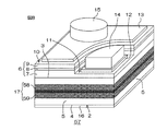
図1は、本発明の第1実施形態に係る半導体発光素子1の斜視図である。図2は、図1のII-II線に沿う縦断面図である。
図1および図2に示されるように、本実施形態に係る半導体発光素子1は、直方体形状の透光性の基板2を含む。基板2は、サファイア基板であってもよい。基板2は、一方表面3と、その反対の他方表面4と、それらを接続する4つの側面5とを有している。基板2の一方表面3上には、本発明の光が生成される半導体層の一例としてのエピタキシャル層6が形成されている。
Hereinafter, embodiments of the present invention will be described in detail with reference to the accompanying drawings.
<First Embodiment>
FIG. 1 is a perspective view of the semiconductor light emitting device 1 according to the first embodiment of the present invention. FIG. 2 is a vertical cross-sectional view taken along the line II-II of FIG.
As shown in FIGS. 1 and 2, the semiconductor light emitting device 1 according to the present embodiment includes a rectangular parallelepiped translucent substrate 2. The substrate 2 may be a sapphire substrate. The substrate 2 has one surface 3 and the opposite surface 4, and four side surfaces 5 connecting them. An epitaxial layer 6 is formed on one surface 3 of the substrate 2 as an example of the semiconductor layer in which the light of the present invention is generated.

エピタキシャル層6は、基板2の一方表面3の全域を覆うように基板2の一方表面3上に形成されている。エピタキシャル層6は、基板2の一方表面3側からこの順に積層されたn型の第1半導体層7、発光層8およびp型の第2半導体層9を含む。第1半導体層7、発光層8および第2半導体層9は、いずれもIII族窒化物半導体を含む。第1半導体層7、発光層8および第2半導体層9は、窒化ガリウム(GaN)を含んでいてもよい。 The epitaxial layer 6 is formed on one surface 3 of the substrate 2 so as to cover the entire area of one surface 3 of the substrate 2. The epitaxial layer 6 includes an n-type first semiconductor layer 7, a light emitting layer 8 and a p-type second semiconductor layer 9 laminated in this order from one surface 3 side of the substrate 2. The first semiconductor layer 7, the light emitting layer 8 and the second semiconductor layer 9 all include a group III nitride semiconductor. The first semiconductor layer 7, the light emitting layer 8 and the second semiconductor layer 9 may contain gallium nitride (GaN).

エピタキシャル層6は、第1半導体層7を露出させるように、第1半導体層7の一部、発光層8および第2半導体層9を選択的に切り欠いて形成されたメサ構造10と、当該メサ構造10の外側の領域であり、第1半導体層7が露出する外方領域11とを有している。外方領域11は、第1半導体層7からなる単層構造を有しており、平面視において基板2の一方表面3における一つの角部に扇形状に形成されている。一方、メサ構造10は、平面視において外方領域11を取り囲むようにL字形状に形成されている。 The epitaxial layer 6 includes a mesa structure 10 formed by selectively cutting out a part of the first semiconductor layer 7, the light emitting layer 8 and the second semiconductor layer 9 so as to expose the first semiconductor layer 7. It is an outer region of the mesa structure 10 and has an outer region 11 where the first semiconductor layer 7 is exposed. The outer region 11 has a single-layer structure composed of the first semiconductor layer 7, and is formed in a fan shape at one corner of one surface 3 of the substrate 2 in a plan view. On the other hand, the mesa structure 10 is formed in an L shape so as to surround the outer region 11 in a plan view.

エピタキシャル層6上には、第1半導体層7に電気的に接続される第1コンタクト電極12と、第2半導体層9に電気的に接続される第2コンタクト電極13とが配置されている。第1コンタクト電極12および第2コンタクト電極13は、たとえば酸化亜鉛(ZnO)または酸化インジウムスズ(ITO)を含む透明電極である。
第1コンタクト電極12は、メサ構造10および基板2の側面5から間隔を空けて、外方領域11に接合されている。第1コンタクト電極12は、本実施形態では、平面視において外方領域11と略相似形状とされた扇形状に形成されている。一方、第2コンタクト電極13は、外方領域11および基板2の側面5から間隔を空けて、メサ構造10における第2半導体層9に接合されている。第2コンタクト電極13は、本実施形態では、メサ構造10と略相似形状とされた平面視L字形状に形成されている。なお、第2コンタクト電極13は、平面視L字形状に限定されることはなく、平面視四角形状やその他任意の形状に形成されていてもよい。
On the epitaxial layer 6, a first contact electrode 12 electrically connected to the first semiconductor layer 7 and a second contact electrode 13 electrically connected to the second semiconductor layer 9 are arranged. The first contact electrode 12 and the second contact electrode 13 are transparent electrodes containing, for example, zinc oxide (ZnO) or indium tin oxide (ITO).
The first contact electrode 12 is joined to the outer region 11 at a distance from the side surface 5 of the mesa structure 10 and the substrate 2. In the present embodiment, the first contact electrode 12 is formed in a fan shape having a shape substantially similar to that of the outer region 11 in a plan view. On the other hand, the second contact electrode 13 is bonded to the second semiconductor layer 9 in the mesa structure 10 at intervals from the outer region 11 and the side surface 5 of the substrate 2. In the present embodiment, the second contact electrode 13 is formed in an L-shape in a plan view having a shape substantially similar to that of the mesa structure 10. The second contact electrode 13 is not limited to the L-shape in a plan view, and may be formed in a quadrangular shape in a plan view or any other shape.

第1コンタクト電極12上には、第1半導体層7に電気的に接続される第1外部端子14が配置されており、第2コンタクト電極13上には、第2半導体層9に電気的に接続される第2外部端子15が配置されている。第1外部端子14および第2外部端子15は、基板2の一つの対角線に沿って互いに間隔を空けて配置されている。第1外部端子14および第2外部端子15は、金(Au)を含んでいてもよい。 A first external terminal 14 electrically connected to the first semiconductor layer 7 is arranged on the first contact electrode 12, and an electric terminal 9 is electrically connected to the second semiconductor layer 9 on the second contact electrode 13. The second external terminal 15 to be connected is arranged. The first external terminal 14 and the second external terminal 15 are arranged so as to be spaced apart from each other along one diagonal line of the substrate 2. The first external terminal 14 and the second external terminal 15 may contain gold (Au).

第1外部端子14は、本実施形態では、平面視において第1コンタクト電極12と略相似形状とされた扇型の柱状に形成されている。なお、第1外部端子14は、扇型の柱状に限定されることはなく、四角柱状、円柱状、またはその他任意の形状に形成されていてもよい。第2外部端子15は、本実施形態では、柱状(本実施形態では円柱状)に形成されている。なお、第2外部端子15は、円柱状に限定されることはなく、扇型の柱状、四角柱状、またはその他任意の形状に形成されていてもよい。 In the present embodiment, the first external terminal 14 is formed in a fan-shaped columnar shape having a shape substantially similar to that of the first contact electrode 12 in a plan view. The first external terminal 14 is not limited to a fan-shaped columnar shape, and may be formed in a square columnar shape, a columnar shape, or any other shape. The second external terminal 15 is formed in a columnar shape (cylindrical shape in the present embodiment) in the present embodiment. The second external terminal 15 is not limited to a columnar shape, and may be formed in a fan-shaped columnar shape, a square columnar shape, or any other shape.

基板2の他方表面4側には、当該基板2の他方表面4の全域を被覆するように、エピタキシャル層6(発光層8)で生成された光をエピタキシャル層6側に向けて反射させるための光反射層16が形成されている。光反射層16は、一つの金属膜からなる単層構造を有していてもよいし、複数の金属膜が積層された積層構造を有していてもよい。光反射層16は、アルミニウム(Al)、金(Au)および銀(Ag)を含む群から選択される1種または2種以上の金属膜によって形成されていてもよい。 The light generated by the epitaxial layer 6 (light emitting layer 8) is reflected toward the epitaxial layer 6 on the other surface 4 side of the substrate 2 so as to cover the entire area of the other surface 4 of the substrate 2. The light reflecting layer 16 is formed. The light reflecting layer 16 may have a single-layer structure composed of one metal film, or may have a laminated structure in which a plurality of metal films are laminated. The light reflecting layer 16 may be formed of one or more metal films selected from the group containing aluminum (Al), gold (Au) and silver (Ag).

また、光反射層16は、屈折率の異なる複数の絶縁膜が積層された積層構造を有する絶縁層であってもよい。光反射層16は、屈折率の異なる絶縁膜が1/4波長の光学長で交互に積層された積層構造を有するDBR(Distributed Bragg Reflector:分布ブラッグ反射)層であってもよい。DBR層は、ZrO、Al、SiO、TiO、Ta、Nb、AlN、SiN、AlONおよびSiONを含む群から選択される2種以上の絶縁膜によって形成されていてもよい。 Further, the light reflecting layer 16 may be an insulating layer having a laminated structure in which a plurality of insulating films having different refractive indexes are laminated. The light reflecting layer 16 may be a DBR (Distributed Bragg Reflector) layer having a laminated structure in which insulating films having different refractive indexes are alternately laminated with an optical length of 1/4 wavelength. The DBR layer is formed by two or more insulating films selected from the group containing ZrO 2 , Al 2 O 3 , SiO 2 , TiO 2 , Ta 2 O 5 , Nb 2 O 5 , AlN, SiN, AlON and SiON. It may have been.

また、光反射層16は、金属膜および絶縁膜(DBR層)の両方を含む積層構造を有していてもよい。この場合、光反射層16は、基板2の他方表面4側から金属膜および絶縁膜(DBR層)を含む積層構造を有していてもよいし、基板2の他方表面4側から絶縁膜(DBR層)および金属膜を含む積層構造を有していてもよい。
図1および図2を参照して、本実施形態に係る半導体発光素子1は、基板2の側面5における一方表面3から他方表面4側に間隔を空けた位置に形成され、基板2を構成する材料が変質することにより他の領域とは異なる物理的特性とされた改質層17を含む。
Further, the light reflecting layer 16 may have a laminated structure including both a metal film and an insulating film (DBR layer). In this case, the light reflecting layer 16 may have a laminated structure including a metal film and an insulating film (DBR layer) from the other surface 4 side of the substrate 2, or the insulating film (DBR layer) from the other surface 4 side of the substrate 2. It may have a laminated structure including a DBR layer) and a metal film.
With reference to FIGS. 1 and 2, the semiconductor light emitting device 1 according to the present embodiment is formed at a position on the side surface 5 of the substrate 2 at a distance from one surface 3 to the other surface 4 to form the substrate 2. It contains a modified layer 17 having physical properties different from those of other regions due to the alteration of the material.

なお、「変質」とは、結晶状態が他の領域とは異なる結晶状態となることを意味する。また、「改質層17」とは、変質によって密度、屈折率、機械的強度(結晶強度)やその他の物理的特性が、他の領域とは異なる状態となった層のことをいう。例えば、改質層17には、溶融した後再度硬化した溶融再硬化層、空孔や亀裂等を含む欠陥層、絶縁破壊によって生じた絶縁破壊層または他の領域とは異なる屈折率を有する屈折率変化層、もしくは、これらの層が混在した層等が含まれる。改質層17は、本実施形態では、レーザ光の照射によって形成された加工痕(レーザ加工痕)でもある。 In addition, "alteration" means that the crystal state becomes a crystal state different from other regions. Further, the "modified layer 17" refers to a layer in which the density, refractive index, mechanical strength (crystal strength) and other physical properties are different from those in other regions due to alteration. For example, the modified layer 17 includes a melt-hardened layer that has been melted and then hardened again, a defect layer that includes pores and cracks, an dielectric breakdown layer that is generated by dielectric breakdown, or a refraction having a refractive index different from that of other regions. A rate change layer or a layer in which these layers are mixed is included. In the present embodiment, the modified layer 17 is also a processing mark (laser processing mark) formed by irradiation with laser light.

改質層17は、基板2の一方表面3および他方表面4と平行な方向に延びるように基板2の側面5に沿って帯状に形成されており、基板2の内側の領域を取り囲んでいる。改質層17は、本実施形態では、基板2の一方表面3および他方表面4から間隔を空けて形成されている。前述の光反射層16は、基板2の他方表面4の全域を被覆している。したがって、改質層17は、平面視において基板2の周縁全域に亘って光反射層16と対向している。なお、改質層17は、必ずしも基板2の周縁全域に亘って連続的に形成されている必要はなく、基板2の側面5に沿って断続的(間欠的)に形成されていてもよい。 The modified layer 17 is formed in a strip shape along the side surface 5 of the substrate 2 so as to extend in a direction parallel to one surface 3 and the other surface 4 of the substrate 2, and surrounds an inner region of the substrate 2. In the present embodiment, the modified layer 17 is formed at intervals from one surface 3 and the other surface 4 of the substrate 2. The light reflecting layer 16 covers the entire area of the other surface 4 of the substrate 2. Therefore, the modified layer 17 faces the light reflecting layer 16 over the entire peripheral edge of the substrate 2 in a plan view. The modified layer 17 does not necessarily have to be continuously formed over the entire peripheral edge of the substrate 2, and may be formed intermittently (intermittently) along the side surface 5 of the substrate 2.

このような構成において、エピタキシャル層6は、一様な材質で基板2の一方表面3側に形成されている。つまり、エピタキシャル層6において、第1半導体層7、発光層8および第2半導体層9は、いずれも、一様な材質で基板2の一方表面3側に形成されている。エピタキシャル層6が一様な材質であるとは、エピタキシャル層6が、改質層17における基板2の材料の変質の影響を全くまたは殆ど受けずに一様な結晶状態で基板2の一方表面3側に形成されていることを意味する。たとえば、改質層17と基板2の一方表面3との間の距離が10μm以上に設定されることにより、改質層17における基板2の材料の変質の影響がエピタキシャル層6に及ぶのを効果的に抑制または防止できる。 In such a configuration, the epitaxial layer 6 is formed of a uniform material on one surface 3 side of the substrate 2. That is, in the epitaxial layer 6, the first semiconductor layer 7, the light emitting layer 8 and the second semiconductor layer 9 are all made of a uniform material and are formed on one surface 3 side of the substrate 2. When the epitaxial layer 6 is made of a uniform material, the epitaxial layer 6 is in a uniform crystalline state with no or little influence of deterioration of the material of the substrate 2 in the modified layer 17, and one surface 3 of the substrate 2 is used. It means that it is formed on the side. For example, by setting the distance between the modified layer 17 and one surface 3 of the substrate 2 to 10 μm or more, it is effective that the influence of the deterioration of the material of the substrate 2 on the modified layer 17 extends to the epitaxial layer 6. Can be suppressed or prevented.

また、光反射層16は、一様な材質で基板2の他方表面4側に形成されている。光反射層16が一様な材質であるとは、光反射層16が、改質層17における基板2の材料の変質の影響を全くまたは殆ど受けずに一様な結晶状態で基板2の他方表面4側に形成されていることを意味する。
半導体発光素子1は、図3に示されるように、発光素子パッケージ21に搭載される。図3は、図1の半導体発光素子1が搭載された発光素子パッケージ21の縦断面図である。図3に示されるように、発光素子パッケージ21は、前述の半導体発光素子1と、半導体発光素子1を支持する支持基板22と、半導体発光素子1に電気的に接続された複数個の端子電極膜23と、半導体発光素子1を封止する封止樹脂24とを含む。
Further, the light reflecting layer 16 is made of a uniform material and is formed on the other surface 4 side of the substrate 2. The light reflecting layer 16 is made of a uniform material, which means that the light reflecting layer 16 is in a uniform crystalline state of the substrate 2 in a uniform crystal state with little or no influence of deterioration of the material of the substrate 2 in the modified layer 17. It means that it is formed on the surface 4 side.
As shown in FIG. 3, the semiconductor light emitting device 1 is mounted on the light emitting device package 21. FIG. 3 is a vertical cross-sectional view of the light emitting device package 21 on which the semiconductor light emitting device 1 of FIG. 1 is mounted. As shown in FIG. 3, the light emitting element package 21 includes the above-mentioned semiconductor light emitting element 1, a support substrate 22 that supports the semiconductor light emitting element 1, and a plurality of terminal electrodes electrically connected to the semiconductor light emitting element 1. The film 23 and a sealing resin 24 for sealing the semiconductor light emitting device 1 are included.

支持基板22は、本実施形態では直方体形状に形成されており、半導体発光素子1が配置される上面25と、その反対側に位置し実装用電極面とされる下面26と、上面25および下面26を接続する4つの側面27とを有している。支持基板22の上面25の中央部には、半導体発光素子1が接合されるダイパッド28が配置されている。半導体発光素子1は、他方表面4を支持基板22の上面25に向けた状態で、光反射層16とダイパッド28とが接合材29を介して接合されることによって、支持基板22に支持されている。 In the present embodiment, the support substrate 22 is formed in a rectangular parallelepiped shape, and has an upper surface 25 on which the semiconductor light emitting element 1 is arranged, a lower surface 26 located on the opposite side thereof and used as a mounting electrode surface, an upper surface 25, and a lower surface. It has four side surfaces 27 connecting the 26s. A die pad 28 to which the semiconductor light emitting element 1 is bonded is arranged at the center of the upper surface 25 of the support substrate 22. The semiconductor light emitting device 1 is supported by the support substrate 22 by joining the light reflecting layer 16 and the die pad 28 via the bonding material 29 with the other surface 4 facing the upper surface 25 of the support substrate 22. There is.

複数個の端子電極膜23には、半導体発光素子1の第1半導体層7に電気的に接続される第1端子電極膜30と、半導体発光素子1の第2半導体層9に電気的に接続される第2端子電極膜31とが含まれる。第1端子電極膜30は、支持基板22の一つの側面27側に配置されており、第2端子電極膜31は、支持基板22における第1端子電極膜30が形成された側面27と対向する側面27側に配置されている。 The plurality of terminal electrode films 23 are electrically connected to the first terminal electrode film 30 electrically connected to the first semiconductor layer 7 of the semiconductor light emitting element 1 and to the second semiconductor layer 9 of the semiconductor light emitting element 1. The second terminal electrode film 31 to be formed is included. The first terminal electrode film 30 is arranged on one side surface 27 side of the support substrate 22, and the second terminal electrode film 31 faces the side surface 27 on the support substrate 22 on which the first terminal electrode film 30 is formed. It is arranged on the side surface 27 side.

第1端子電極膜30および第2端子電極膜31は、それぞれ支持基板22の上面25に設けられた上面電極膜30a,31aと、支持基板22の下面26に設けられた下面電極膜30b,31bと、上面電極膜30a,31aと下面電極膜30b,31bとを接続する接続部30c,31cとを有している。図3では、接続部30c,31cが、支持基板22の側面27に設けられた接続電極膜である例が示されているが、接続部30c,31cは、支持基板22を貫通して上面電極膜30a,31aと下面電極膜30b,31bとを電気的に接続するビア電極であってもよい。 The first terminal electrode film 30 and the second terminal electrode film 31 are the upper surface electrode films 30a and 31a provided on the upper surface 25 of the support substrate 22, and the lower surface electrode films 30b and 31b provided on the lower surface 26 of the support substrate 22, respectively. And the connecting portions 30c and 31c for connecting the upper surface electrode films 30a and 31a and the lower surface electrode films 30b and 31b. FIG. 3 shows an example in which the connecting portions 30c and 31c are connection electrode films provided on the side surface 27 of the support substrate 22, but the connecting portions 30c and 31c penetrate the support substrate 22 and are top electrodes. It may be a via electrode that electrically connects the films 30a and 31a and the bottom electrode films 30b and 31b.

第1端子電極膜30は、第1外部端子14と上面電極膜30aとが、たとえばボンディングワイヤ等の導線32を介して電気的に接続されることによって、半導体発光素子1に電気的に接続されている。第2端子電極膜31は、第2外部端子15と上面電極膜31aとが、たとえばボンディングワイヤ等の導線33を介して電気的に接続されることによって、半導体発光素子1に電気的に接続されている。 The first terminal electrode film 30 is electrically connected to the semiconductor light emitting element 1 by electrically connecting the first external terminal 14 and the upper surface electrode film 30a via, for example, a conducting wire 32 such as a bonding wire. ing. The second terminal electrode film 31 is electrically connected to the semiconductor light emitting element 1 by electrically connecting the second external terminal 15 and the upper surface electrode film 31a via, for example, a conducting wire 33 such as a bonding wire. ing.

支持基板22の上面25には、半導体発光素子1を取り囲む枠部材34が設けられている。枠部材34は、半導体発光素子1から離れる方向に上り傾斜する傾斜部35を有している。枠部材34は、半導体発光素子1の光を反射させる反射板を兼ねていてもよい。枠部材34は、支持基板22と一体的に設けられていてもよいし、別体として設けられていてもよい。枠部材34は、たとえば白色樹脂を含んでいてもよい。 A frame member 34 surrounding the semiconductor light emitting element 1 is provided on the upper surface 25 of the support substrate 22. The frame member 34 has an inclined portion 35 that inclines upward in a direction away from the semiconductor light emitting element 1. The frame member 34 may also serve as a reflector that reflects the light of the semiconductor light emitting element 1. The frame member 34 may be provided integrally with the support substrate 22, or may be provided as a separate body. The frame member 34 may contain, for example, a white resin.

封止樹脂24は、支持基板22の上面25において、半導体発光素子1を封止するように枠部材34により取り囲まれた空間内を埋めている。封止樹脂24は、透明の樹脂材料からなり、たとえばシリコン、アクリル樹脂またはエポキシ樹脂を含んでいてもよい。
このような発光素子パッケージ21は、支持基板22に半導体発光素子1を実装した後、当該支持基板22と枠部材34とによって区画される空間内に封止樹脂24を供給することによって製造される。なお、発光素子パッケージ21は、枠部材34を有さずに、半導体発光素子1が支持基板22上において封止樹脂24により封止された構成を有していてもよい。このような構成は、たとえば金型を用いたモールド成形法によって、半導体発光素子1を封止するように支持基板22上に封止樹脂24を供給することによって製造できる。
The sealing resin 24 fills the space surrounded by the frame member 34 on the upper surface 25 of the support substrate 22 so as to seal the semiconductor light emitting element 1. The sealing resin 24 is made of a transparent resin material and may contain, for example, a silicone, acrylic resin or epoxy resin.
Such a light emitting element package 21 is manufactured by mounting the semiconductor light emitting element 1 on the support substrate 22 and then supplying the sealing resin 24 into the space partitioned by the support substrate 22 and the frame member 34. .. The light emitting element package 21 may have a configuration in which the semiconductor light emitting element 1 is sealed with the sealing resin 24 on the support substrate 22 without having the frame member 34. Such a configuration can be manufactured by supplying the sealing resin 24 on the support substrate 22 so as to seal the semiconductor light emitting element 1 by, for example, a molding method using a mold.

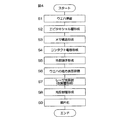
次に、本実施形態に係る半導体発光素子1の製造方法の一例について説明する。図4は、図1の半導体発光素子1の製造方法の一工程を示す工程図である。図5A〜図5Hは、図1の半導体発光素子1の製造工程の一工程を示す縦断面図である。図5A〜図5Hでは、2つの半導体発光素子1が製造される部分の縦断面図を示している。以下では、半導体発光素子1が形成される領域を素子形成領域45という。 Next, an example of the manufacturing method of the semiconductor light emitting device 1 according to the present embodiment will be described. FIG. 4 is a process diagram showing one step of the manufacturing method of the semiconductor light emitting device 1 of FIG. 5A to 5H are vertical cross-sectional views showing one step of the manufacturing process of the semiconductor light emitting device 1 of FIG. 5A to 5H show vertical cross-sectional views of a portion where two semiconductor light emitting elements 1 are manufactured. Hereinafter, the region in which the semiconductor light emitting device 1 is formed is referred to as an element forming region 45.

半導体発光素子1を製造するに当たり、まず、図5Aを参照して、ウエハ42が準備される(図4のステップS1)。ウエハ42は、基板2の基となる単結晶サファイアウエハであり、基板2の一方表面3および他方表面4のそれぞれに対応する一方表面43および他方表面44を有している。次に、図5Bを参照して、エピタキシャル成長法によって、ウエハ42の一方表面43側に、n型の第1半導体層7、発光層8およびp型の第2半導体層9が順に形成される(図4のステップS2)。これにより、ウエハ42の一方表面43側に、当該ウエハ42の一方表面43の全域を被覆するエピタキシャル層6が形成される。 In manufacturing the semiconductor light emitting device 1, first, the wafer 42 is prepared with reference to FIG. 5A (step S1 in FIG. 4). The wafer 42 is a single crystal sapphire wafer on which the substrate 2 is based, and has one surface 43 and the other surface 44 corresponding to one surface 3 and the other surface 4 of the substrate 2, respectively. Next, referring to FIG. 5B, an n-type first semiconductor layer 7, a light emitting layer 8 and a p-type second semiconductor layer 9 are sequentially formed on one surface 43 side of the wafer 42 by an epitaxial growth method (see FIG. 5B). Step S2 in FIG. 4). As a result, the epitaxial layer 6 that covers the entire surface of the one surface 43 of the wafer 42 is formed on the one surface 43 side of the wafer 42.

次に、図5Cを参照して、たとえばマスクを介するエッチングにより、第1半導体層7の一部、発光層8および第2半導体層9の不要な部分が選択的に除去される(図4のステップS3)。これにより、第1半導体層7の一部、発光層8および第2半導体層9を選択的に切り欠いたメサ構造10と、その外側の外方領域11とを含むエピタキシャル層6が各素子形成領域45に形成される。 Next, with reference to FIG. 5C, a part of the first semiconductor layer 7, an unnecessary part of the light emitting layer 8 and the second semiconductor layer 9 are selectively removed by etching through, for example, a mask (FIG. 4). Step S3). As a result, the epitaxial layer 6 including a part of the first semiconductor layer 7, the light emitting layer 8 and the mesa structure 10 in which the second semiconductor layer 9 is selectively cut out, and the outer region 11 outside the mesa structure 10 is formed. It is formed in the region 45.

次に、図5Dを参照して、たとえばスパッタ法により、第1コンタクト電極12および第2コンタクト電極13となる透明導電材料が、エピタキシャル層6上に堆積されて透明導電材料層が形成される(図4のステップS4)。次に、たとえばマスクを介するエッチングにより、透明導電材料層が選択的にパターニングされて、第1コンタクト電極12および第2コンタクト電極13が各素子形成領域45に形成される。 Next, referring to FIG. 5D, the transparent conductive material to be the first contact electrode 12 and the second contact electrode 13 is deposited on the epitaxial layer 6 to form the transparent conductive material layer by, for example, a sputtering method (see FIG. Step S4 in FIG. 4). Next, for example, by etching through a mask, the transparent conductive material layer is selectively patterned, and the first contact electrode 12 and the second contact electrode 13 are formed in each element forming region 45.

次に、たとえばリフトオフ法により、第1外部端子14が第1コンタクト電極12上に形成され、第2外部端子15が第2コンタクト電極13上に形成される(図4のステップS5)。より具体的には、第1外部端子14および第2外部端子15を形成すべき領域に開口を選択的に有するマスクがエピタキシャル層6上に形成される。次に、たとえばスパッタ法等によって、第1外部端子14および第2外部端子15となる導電材料(たとえば金(Au))が開口を埋めるように堆積される。その後、マスクが除去されることによって、第1外部端子14および第2外部端子15が同時に形成される。 Next, for example, by the lift-off method, the first external terminal 14 is formed on the first contact electrode 12, and the second external terminal 15 is formed on the second contact electrode 13 (step S5 in FIG. 4). More specifically, a mask having an opening selectively in the region where the first external terminal 14 and the second external terminal 15 should be formed is formed on the epitaxial layer 6. Next, for example, by a sputtering method or the like, a conductive material (for example, gold (Au)) to be the first external terminal 14 and the second external terminal 15 is deposited so as to fill the opening. After that, by removing the mask, the first external terminal 14 and the second external terminal 15 are formed at the same time.

次に、図5Eを参照して、ウエハ42の一方表面43側から当該ウエハ42を固定支持する支持部材46がウエハ42に貼付される。本実施形態では、支持部材46は、粘着テープ47を介してウエハ42に貼付される。支持部材46は、粘着テープ47に代えて、貼付用ワックスを介してウエハ42に密着するように貼付されてもよい。
なお、支持部材46は、後の工程で、ウエハ42から剥離可能な部材であればどのような部材であってもよい。支持部材46は、シリコン製の基板、ガラス製の基板、または、金属製(たとえば銅製やステンレス製)の基板であってもよいし、ウエハ42を支持するのに十分な強度を有するテープ部材であってもよい。
Next, with reference to FIG. 5E, a support member 46 for fixing and supporting the wafer 42 is attached to the wafer 42 from one surface 43 side of the wafer 42. In the present embodiment, the support member 46 is attached to the wafer 42 via the adhesive tape 47. Instead of the adhesive tape 47, the support member 46 may be attached so as to be in close contact with the wafer 42 via a sticking wax.
The support member 46 may be any member as long as it can be peeled off from the wafer 42 in a later step. The support member 46 may be a silicon substrate, a glass substrate, a metal (for example, copper or stainless steel) substrate, or a tape member having sufficient strength to support the wafer 42. There may be.

次に、たとえばCMP(Chemical Mechanical Polishing:化学機械研磨)法によって、ウエハ42の厚さが所望の厚さとなるまでウエハ42の他方表面44が研削されると同時に、ウエハ42の他方表面44が滑面化または鏡面化される(図4のステップS6)。
次に、図5Fを参照して、レーザ光照射装置48を用いて、ウエハ42内にレーザ光が照射される(図4のステップS7)。より具体的には、ウエハ42内における一方表面43から他方表面44側に間隔を空けた領域に集光点が合わされて、ウエハ42の他方表面44側からレーザ光が照射される。レーザ光は、各素子形成領域45を区画するようにウエハ42内に照射される。この時、ウエハ42の他方表面44が滑面化または鏡面化されているから、ウエハ42内にレーザ光を良好に照射させることができる。
Next, for example, by a CMP (Chemical Mechanical Polishing) method, the other surface 44 of the wafer 42 is ground until the thickness of the wafer 42 reaches a desired thickness, and at the same time, the other surface 44 of the wafer 42 slides. It is surfaced or mirrored (step S6 in FIG. 4).
Next, referring to FIG. 5F, the laser beam is irradiated into the wafer 42 by using the laser beam irradiation device 48 (step S7 in FIG. 4). More specifically, the condensing points are aligned with the regions of the wafer 42 spaced from one surface 43 to the other surface 44, and the laser beam is irradiated from the other surface 44 side of the wafer 42. The laser beam is irradiated into the wafer 42 so as to partition each element forming region 45. At this time, since the other surface 44 of the wafer 42 is smoothed or mirrored, the inside of the wafer 42 can be satisfactorily irradiated with the laser beam.

このレーザ光の照射工程により、ウエハ42を構成する材料(サファイア)が変質し、他の領域とは異なる物理的特性とされた改質層17がウエハ42内形成される。より具体的には、本実施形態では、改質層17は、レーザ光の照射によるレーザ加工痕であり、ウエハ42の一方表面43から他方表面44側に間隔を空けた位置に形成される。この改質層17は、少なくとも他の領域の結晶強度よりも小さい結晶強度を有しており、この改質層17によってウエハ42を分割するための分割起点が形成される。 By this laser beam irradiation step, the material (sapphire) constituting the wafer 42 is altered, and a modified layer 17 having physical characteristics different from those of other regions is formed in the wafer 42. More specifically, in the present embodiment, the modified layer 17 is a laser machining mark generated by irradiation with laser light, and is formed at a position spaced from one surface 43 of the wafer 42 to the other surface 44 side. The modified layer 17 has a crystal strength smaller than the crystal strength of at least other regions, and the modified layer 17 forms a division starting point for dividing the wafer 42.

次に、図5Gを参照して、たとえばCVD法、スパッタ法または蒸着法によって導電材料または絶縁材料が選択的にウエハ42の他方表面44側に堆積されて、光反射層16が形成される(図4のステップS8)。光反射層16は、たとえばウエハ42の他方表面44の全域または略全域を被覆するようにウエハ42の他方表面44側に形成される。
この工程において、一つの金属膜からなる単層構造を有する光反射層16が形成されてもよいし、複数の金属膜が積層された積層構造を有する光反射層16が形成されてもよい。また、屈折率の異なる複数の絶縁膜が積層された積層構造を有する光反射層16が形成されてもよい。光反射層16として、屈折率の異なる絶縁膜が1/4波長の光学長で交互に積層された積層構造を有するDBR層が形成されてもよい。また、金属膜および絶縁膜(DBR層)の両方を含む積層構造を有する光反射層16が形成されてもよい。
Next, with reference to FIG. 5G, the conductive material or the insulating material is selectively deposited on the other surface 44 side of the wafer 42 by, for example, a CVD method, a sputtering method or a vapor deposition method, and the light reflecting layer 16 is formed ( Step S8 in FIG. 4). The light reflecting layer 16 is formed on the other surface 44 side of the wafer 42 so as to cover the entire area or substantially the entire area of the other surface 44 of the wafer 42, for example.
In this step, a light reflecting layer 16 having a single layer structure made of one metal film may be formed, or a light reflecting layer 16 having a laminated structure in which a plurality of metal films are laminated may be formed. Further, the light reflecting layer 16 having a laminated structure in which a plurality of insulating films having different refractive indexes are laminated may be formed. As the light reflecting layer 16, a DBR layer having a laminated structure in which insulating films having different refractive indexes are alternately laminated with an optical length of 1/4 wavelength may be formed. Further, a light reflecting layer 16 having a laminated structure including both a metal film and an insulating film (DBR layer) may be formed.

次に、図5Hを参照して、支持部材46が剥離されて、ウエハ42の他方表面44側に、当該ウエハ42を支持するための柔軟なテープ部材49が貼付される。次に、たとえば劈開ブレード50等によって、テープ部材49越しに、ウエハ42の他方表面44側から改質層17に対して外力が加えられて、改質層17を分割起点として、エピタキシャル層6および光反射層16と共にウエハ42が劈開(分割)される。これにより、複数個の半導体発光素子1の個片がウエハ42から切り出される。 Next, referring to FIG. 5H, the support member 46 is peeled off, and a flexible tape member 49 for supporting the wafer 42 is attached to the other surface 44 side of the wafer 42. Next, for example, an external force is applied to the modified layer 17 from the other surface 44 side of the wafer 42 through the tape member 49 by, for example, a cleavage blade 50, and the epitaxial layer 6 and the epitaxial layer 6 and the modified layer 17 are used as a starting point for division. The wafer 42 is cleaved (divided) together with the light reflecting layer 16. As a result, individual pieces of the plurality of semiconductor light emitting elements 1 are cut out from the wafer 42.

なお、本実施形態では、ウエハ42の他方表面44側から改質層17に外力が加えられる例について説明したが、ウエハ42の一方表面43側にテープ部材49が貼付されて、当該ウエハ42の一方表面43側から改質層17に外力が加えられてもよい。
以上、本実施形態に係る半導体発光素子1の製造方法では、改質層形成工程(図4のステップS7)の後、ウエハ42の他方表面44側に光反射層16を形成し(図4のステップS8)、当該改質層17を分割起点として、エピタキシャル層6および光反射層16と共にウエハ42を劈開(分割)している(図4のステップS9)。この分割されたウエハ42が半導体発光素子1の一部を構成する基板2となる。したがって、光反射層16を除去することなく、基板2の他方表面4の全域が光反射層16によって被覆された構成を有する半導体発光素子1を製造できる。
In the present embodiment, an example in which an external force is applied to the modified layer 17 from the other surface 44 side of the wafer 42 has been described, but the tape member 49 is attached to the one surface 43 side of the wafer 42, and the wafer 42 is attached. On the other hand, an external force may be applied to the modified layer 17 from the surface 43 side.
As described above, in the method for manufacturing the semiconductor light emitting device 1 according to the present embodiment, after the modified layer forming step (step S7 in FIG. 4), the light reflecting layer 16 is formed on the other surface 44 side of the wafer 42 (FIG. 4). In step S8), the wafer 42 is cleaved (divided) together with the epitaxial layer 6 and the light reflecting layer 16 with the modified layer 17 as the division starting point (step S9 in FIG. 4). The divided wafer 42 becomes the substrate 2 that forms a part of the semiconductor light emitting element 1. Therefore, the semiconductor light emitting device 1 having a configuration in which the entire other surface 4 of the substrate 2 is covered with the light reflecting layer 16 can be manufactured without removing the light reflecting layer 16.

これにより、光反射層16を除去する工程を実行する必要がなくなり、当該光反射層16を除去するための装置を別途準備する必要もなくなるから、半導体発光素子1のコストを削減できる。
たとえば、光反射層16を除去することなく当該光反射層16を介して基板2にレーザ光を照射する方法も考えられる。しかし、この場合には、光反射層16によってレーザ光の一部が反射されたり、当該光反射層16が障壁となったりするから、ウエハ42の内部に改質層17を良好に形成できない虞がある。これに対して、本実施形態の製造方法によれば、改質層形成工程(図4のステップS7)の後に光反射層16を形成しているので、光反射層16を介して基板2にレーザ光が照射されることがない。これにより、ウエハ42の内部に改質層17を良好に形成できるから、半導体発光素子1を良好に個片化できる。
As a result, it is not necessary to execute the step of removing the light reflecting layer 16, and it is not necessary to separately prepare a device for removing the light reflecting layer 16, so that the cost of the semiconductor light emitting element 1 can be reduced.
For example, a method of irradiating the substrate 2 with a laser beam through the light reflecting layer 16 without removing the light reflecting layer 16 is also conceivable. However, in this case, a part of the laser beam is reflected by the light reflecting layer 16 or the light reflecting layer 16 acts as a barrier, so that the modified layer 17 may not be satisfactorily formed inside the wafer 42. There is. On the other hand, according to the manufacturing method of the present embodiment, since the light reflecting layer 16 is formed after the modified layer forming step (step S7 in FIG. 4), the light reflecting layer 16 is formed on the substrate 2 via the light reflecting layer 16. No laser beam is applied. As a result, the modified layer 17 can be satisfactorily formed inside the wafer 42, so that the semiconductor light emitting device 1 can be satisfactorily separated.

また、改質層形成工程(図4のステップS7)の後に光反射層16を形成しているので、レーザ光の照射によるダメージが光反射層16に入らない。したがって、光反射層16を一様な材質でウエハ42の他方表面44側に形成できる。これにより、エピタキシャル層6(発光層8)で生成された光を良好に反射させることが可能な光反射層16を形成できるから、輝度を良好に向上させることができる。 Further, since the light reflecting layer 16 is formed after the modified layer forming step (step S7 in FIG. 4), the light reflecting layer 16 is not damaged by the irradiation of the laser beam. Therefore, the light reflecting layer 16 can be formed on the other surface 44 side of the wafer 42 with a uniform material. As a result, the light reflecting layer 16 capable of satisfactorily reflecting the light generated by the epitaxial layer 6 (light emitting layer 8) can be formed, so that the brightness can be satisfactorily improved.

さらに、本実施形態の製造方法によれば、ウエハ42内における一方表面43から他方表面44側に間隔を空けた領域に集光点を合わせてウエハ42の他方表面44側からレーザ光を照射しているから、エピタキシャル層6を一様な材質でウエハ42の一方表面43側に形成できる。これにより、エピタキシャル層6で光を良好に生成させることができるから、このような観点からも、輝度を良好に向上させることができる。 Further, according to the manufacturing method of the present embodiment, a condensing point is set in a region of the wafer 42 spaced from one surface 43 to the other surface 44 side, and laser light is irradiated from the other surface 44 side of the wafer 42. Therefore, the epitaxial layer 6 can be formed on one surface 43 side of the wafer 42 with a uniform material. As a result, light can be satisfactorily generated in the epitaxial layer 6, and thus the brightness can be satisfactorily improved from such a viewpoint as well.

また、本実施形態に係る半導体発光素子1の製造方法によれば、研磨工程(図4のステップS6)に先立って、支持部材46をウエハ42の一方表面43側に貼付する工程を含む。研磨工程によってウエハ42が薄化されるためウエハ42の強度が低下することになるが、本実施形態に係る半導体発光素子1の製造方法によれば、支持部材46によってウエハ42を固定支持できる。これにより、研磨工程(図4のステップS6)を良好に実行することができる。また、支持部材46によってウエハ42を固定支持することによって、研磨工程(図4のステップS6)後の工程、つまり、改質層形成工程(図4のステップS7)や光反射層形成工程(図4のステップS8)も良好に実行できる。 Further, according to the method for manufacturing the semiconductor light emitting device 1 according to the present embodiment, a step of attaching the support member 46 to one surface 43 side of the wafer 42 is included prior to the polishing step (step S6 of FIG. 4). Since the wafer 42 is thinned by the polishing step, the strength of the wafer 42 is lowered. However, according to the method for manufacturing the semiconductor light emitting element 1 according to the present embodiment, the wafer 42 can be fixedly supported by the support member 46. As a result, the polishing step (step S6 in FIG. 4) can be satisfactorily executed. Further, by fixing and supporting the wafer 42 by the support member 46, the steps after the polishing step (step S6 in FIG. 4), that is, the modified layer forming step (step S7 in FIG. 4) and the light reflecting layer forming step (FIG. 4). Step S8) of 4 can also be performed satisfactorily.

<第2実施形態>
図6は、本発明の第2実施形態に係る半導体発光素子51の斜視図である。図6において、前述の第1実施形態において述べた構成と同様の構成については同一の参照符号を付して説明を省略する。
図6を参照して、本実施形態に係る改質層17は、基板2の一方表面3側に形成された第1改質層52と、基板2の他方表面4側に形成された第2改質層53とを含む。第1改質層52および第2改質層53は、互いに間隔を空けて形成されている。第1改質層52および第2改質層53は、いずれも基板2の一方表面3および他方表面4と平行な方向に延びるように基板2の側面5に沿って帯状に形成されており、基板2の内側の領域を取り囲んでいる。
<Second Embodiment>
FIG. 6 is a perspective view of the semiconductor light emitting device 51 according to the second embodiment of the present invention. In FIG. 6, the same reference numerals are given to the same configurations as those described in the first embodiment described above, and the description thereof will be omitted.
With reference to FIG. 6, the modified layer 17 according to the present embodiment has a first modified layer 52 formed on one surface 3 side of the substrate 2 and a second modified layer 52 formed on the other surface 4 side of the substrate 2. Includes a modified layer 53. The first modified layer 52 and the second modified layer 53 are formed at intervals from each other. The first modified layer 52 and the second modified layer 53 are both formed in a strip shape along the side surface 5 of the substrate 2 so as to extend in a direction parallel to one surface 3 and the other surface 4 of the substrate 2. It surrounds the inner region of the substrate 2.

第1改質層52は、基板2の一方表面3から他方表面4側に間隔を空けた位置に形成されている。第2改質層53は、基板の他方表面4から一方表面3側に間隔を空けた位置に形成されている。なお、第1改質層52および第2改質層53は、必ずしも基板2の周縁全域に亘って連続的に形成されている必要はなく、基板2の側面5に沿って断続的(間欠的)に形成されていてもよい。 The first modified layer 52 is formed at a position spaced from one surface 3 of the substrate 2 to the other surface 4 side. The second modified layer 53 is formed at a position spaced from the other surface 4 of the substrate to the one surface 3 side. The first modified layer 52 and the second modified layer 53 do not necessarily have to be continuously formed over the entire peripheral edge of the substrate 2, and are intermittent (intermittent) along the side surface 5 of the substrate 2. ) May be formed.

第1改質層52および第2改質層53を含む改質層17は、前述の改質層形成工程(図4のステップS7)において、ウエハ42の厚さ方向の異なる位置にレーザ光を多段階照射(本実施形態では2段階照射)することにより形成できる。このような構成によっても、前述の第1実施形態において述べた効果と同様の効果を奏することができる。
<第3実施形態>
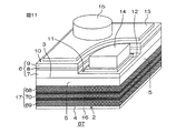
図7は、本発明の第3実施形態に係る半導体発光素子54の斜視図である。図7において、前述の第1実施形態において述べた構成と同様の構成については同一の参照符号を付して説明を省略する。
The modified layer 17 including the first modified layer 52 and the second modified layer 53 emits laser light to different positions in the thickness direction of the wafer 42 in the above-mentioned modified layer forming step (step S7 in FIG. 4). It can be formed by multi-step irradiation (two-step irradiation in this embodiment). Even with such a configuration, the same effect as that described in the above-described first embodiment can be obtained.
<Third Embodiment>
FIG. 7 is a perspective view of the semiconductor light emitting device 54 according to the third embodiment of the present invention. In FIG. 7, the same reference numerals are given to the same configurations as those described in the first embodiment described above, and the description thereof will be omitted.

図7を参照して、本実施形態に係る改質層17は、基板2の一方表面3側に形成された第1改質層55と、基板2の他方表面4側に形成された第2改質層56とを含む。第1改質層55および第2改質層56は、互いに間隔を空けて形成されている。第1改質層55および第2改質層56は、いずれも基板2の一方表面3および他方表面4と平行な方向に延びるように基板2の側面5に沿って帯状に形成されており、基板2の内側の領域を取り囲んでいる。 With reference to FIG. 7, the modified layer 17 according to the present embodiment has a first modified layer 55 formed on one surface 3 side of the substrate 2 and a second modified layer 17 formed on the other surface 4 side of the substrate 2. Includes a modified layer 56. The first modified layer 55 and the second modified layer 56 are formed at intervals from each other. The first modified layer 55 and the second modified layer 56 are both formed in a strip shape along the side surface 5 of the substrate 2 so as to extend in a direction parallel to one surface 3 and the other surface 4 of the substrate 2. It surrounds the inner region of the substrate 2.

第1改質層55は、基板2の一方表面3から他方表面4側に間隔を空けた位置に形成されている。第2改質層56は、基板2の他方表面4から露出するように形成されている。前述の光反射層16は、基板2の他方表面4側において第2改質層56と接している。なお、第1改質層55および第2改質層56は、必ずしも基板2の周縁全域に亘って連続的に形成されている必要はなく、基板2の側面5に沿って断続的(間欠的)に形成されていてもよい。 The first modified layer 55 is formed at a position spaced from one surface 3 of the substrate 2 to the other surface 4 side. The second modified layer 56 is formed so as to be exposed from the other surface 4 of the substrate 2. The above-mentioned light reflecting layer 16 is in contact with the second modified layer 56 on the other surface 4 side of the substrate 2. The first modified layer 55 and the second modified layer 56 do not necessarily have to be continuously formed over the entire peripheral edge of the substrate 2, and are intermittent (intermittent) along the side surface 5 of the substrate 2. ) May be formed.

第1改質層55および第2改質層56を含む改質層17は、前述の改質層形成工程(図4のステップS7)において、ウエハ42の厚さ方向の異なる位置にレーザ光を多段階照射(本実施形態では2段階照射)することにより形成できる。このような構成によっても、前述の第1実施形態において述べた効果と同様の効果を奏することができる。
<第4実施形態>
図8は、本発明の第4実施形態に係る半導体発光素子57の斜視図である。図8において、前述の第1実施形態において述べた構成と同様の構成については同一の参照符号を付して説明を省略する。
The modified layer 17 including the first modified layer 55 and the second modified layer 56 emits laser light to different positions in the thickness direction of the wafer 42 in the above-mentioned modified layer forming step (step S7 in FIG. 4). It can be formed by multi-step irradiation (two-step irradiation in this embodiment). Even with such a configuration, the same effect as that described in the above-described first embodiment can be obtained.
<Fourth Embodiment>
FIG. 8 is a perspective view of the semiconductor light emitting device 57 according to the fourth embodiment of the present invention. In FIG. 8, the same reference numerals are given to the same configurations as those described in the first embodiment described above, and the description thereof will be omitted.

図8を参照して、本実施形態に係る改質層17は、基板2の一方表面3側に形成された第1改質層58と、基板2の他方表面4側に形成された第2改質層59とを含む。第1改質層58および第2改質層59は、基板2の厚さ方向に互いに重なるように形成されている。第1改質層58および第2改質層59は、いずれも基板2の一方表面3および他方表面4と平行な方向に延びるように基板2の側面5に沿って帯状に形成されており、基板2の内側の領域を取り囲んでいる。つまり、本実施形態に係る改質層17は、第1改質層58および第2改質層59が重なる帯状の重複部を有している。 With reference to FIG. 8, the modified layer 17 according to the present embodiment has a first modified layer 58 formed on one surface 3 side of the substrate 2 and a second modified layer 58 formed on the other surface 4 side of the substrate 2. Includes a modified layer 59. The first modified layer 58 and the second modified layer 59 are formed so as to overlap each other in the thickness direction of the substrate 2. Both the first modified layer 58 and the second modified layer 59 are formed in a strip shape along the side surface 5 of the substrate 2 so as to extend in a direction parallel to one surface 3 and the other surface 4 of the substrate 2. It surrounds the inner region of the substrate 2. That is, the modified layer 17 according to the present embodiment has a band-shaped overlapping portion in which the first modified layer 58 and the second modified layer 59 overlap.

第1改質層58は、基板2の一方表面3から他方表面4側に間隔を空けた位置に形成されている。第2改質層59は、基板2の他方表面4から一方表面3側に間隔を空けた位置に形成されている。なお、第1改質層58および第2改質層59は、必ずしも基板2の周縁全域に亘って連続的に形成されている必要はなく、基板2の側面5に沿って断続的(間欠的)に形成されていてもよい。 The first modified layer 58 is formed at a position spaced from one surface 3 of the substrate 2 to the other surface 4 side. The second modified layer 59 is formed at a position spaced from the other surface 4 of the substrate 2 to the one surface 3 side. The first modified layer 58 and the second modified layer 59 do not necessarily have to be continuously formed over the entire peripheral edge of the substrate 2, and are intermittent (intermittent) along the side surface 5 of the substrate 2. ) May be formed.

第1改質層58および第2改質層59を含む改質層17は、前述の改質層形成工程(図4のステップS7)において、ウエハ42の厚さ方向の異なる位置にレーザ光を多段階照射(本実施形態では2段階照射)することにより形成できる。このような構成によっても、前述の第1実施形態において述べた効果と同様の効果を奏することができる。
<第5実施形態>
図9は、本発明の第5実施形態に係る半導体発光素子60の斜視図である。図9において、前述の第1実施形態において述べた構成と同様の構成については同一の参照符号を付して説明を省略する。
The modified layer 17 including the first modified layer 58 and the second modified layer 59 emits laser light to different positions in the thickness direction of the wafer 42 in the above-mentioned modified layer forming step (step S7 in FIG. 4). It can be formed by multi-step irradiation (two-step irradiation in this embodiment). Even with such a configuration, the same effect as that described in the above-described first embodiment can be obtained.
<Fifth Embodiment>
FIG. 9 is a perspective view of the semiconductor light emitting device 60 according to the fifth embodiment of the present invention. In FIG. 9, the same reference numerals are given to the same configurations as those described in the first embodiment described above, and the description thereof will be omitted.

図9を参照して、本実施形態に係る改質層17は、基板2の一方表面3側に形成された第1改質層61と、基板2の他方表面4側に形成された第2改質層62とを含む。第1改質層61および第2改質層62は、基板2の厚さ方向に互いに重なるように形成されている。第1改質層61および第2改質層62は、いずれも基板2の一方表面3および他方表面4と平行な方向に延びるように基板2の側面5に沿って帯状に形成されており、基板2の内側の領域を取り囲んでいる。つまり、本実施形態に係る改質層17は、第1改質層61および第2改質層62が重なる帯状の重複部を有している。 With reference to FIG. 9, the modified layer 17 according to the present embodiment has a first modified layer 61 formed on one surface 3 side of the substrate 2 and a second modified layer 17 formed on the other surface 4 side of the substrate 2. Includes a modified layer 62. The first modified layer 61 and the second modified layer 62 are formed so as to overlap each other in the thickness direction of the substrate 2. Both the first modified layer 61 and the second modified layer 62 are formed in a strip shape along the side surface 5 of the substrate 2 so as to extend in a direction parallel to one surface 3 and the other surface 4 of the substrate 2. It surrounds the inner region of the substrate 2. That is, the modified layer 17 according to the present embodiment has a band-shaped overlapping portion in which the first modified layer 61 and the second modified layer 62 overlap.

第1改質層61は、基板2の一方表面3から他方表面4側に間隔を空けた位置に形成されている。第2改質層62は、基板2の他方表面4から露出するように形成されている。なお、第1改質層61および第2改質層62は、必ずしも基板2の周縁全域に亘って連続的に形成されている必要はなく、基板2の側面5に沿って断続的(間欠的)に形成されていてもよい。 The first modified layer 61 is formed at a position spaced from one surface 3 of the substrate 2 to the other surface 4 side. The second modified layer 62 is formed so as to be exposed from the other surface 4 of the substrate 2. The first modified layer 61 and the second modified layer 62 do not necessarily have to be continuously formed over the entire peripheral edge of the substrate 2, and are intermittent (intermittent) along the side surface 5 of the substrate 2. ) May be formed.

第1改質層61および第2改質層62を含む改質層17は、前述の改質層形成工程(図4のステップS7)において、ウエハ42の厚さ方向の異なる位置にレーザ光を多段階照射(本実施形態では2段階照射)することにより形成できる。このような構成によっても、前述の第1実施形態において述べた効果と同様の効果を奏することができる。
<第6実施形態>
図10は、本発明の第6実施形態に係る半導体発光素子63の斜視図である。図10において、前述の第1実施形態において述べた構成と同様の構成については同一の参照符号を付して説明を省略する。
The modified layer 17 including the first modified layer 61 and the second modified layer 62 emits laser light to different positions in the thickness direction of the wafer 42 in the above-mentioned modified layer forming step (step S7 in FIG. 4). It can be formed by multi-step irradiation (two-step irradiation in this embodiment). Even with such a configuration, the same effect as that described in the above-described first embodiment can be obtained.
<Sixth Embodiment>
FIG. 10 is a perspective view of the semiconductor light emitting device 63 according to the sixth embodiment of the present invention. In FIG. 10, the same reference numerals are given to the same configurations as those described in the first embodiment described above, and the description thereof will be omitted.

図10を参照して、本実施形態に係る改質層17は、基板2の一方表面3側に形成された第1改質層64と、基板2の他方表面4側に形成された第2改質層65と、第1改質層64および第2改質層65の間に形成された中間改質層66とを含む。第1改質層64および中間改質層66は、基板2の厚さ方向に互いに重なるように形成されている。第2改質層65および中間改質層66は、基板2の厚さ方向に互いに重なるように形成されている。 With reference to FIG. 10, the modified layer 17 according to the present embodiment has a first modified layer 64 formed on one surface 3 side of the substrate 2 and a second modified layer 64 formed on the other surface 4 side of the substrate 2. It includes a modified layer 65 and an intermediate modified layer 66 formed between the first modified layer 64 and the second modified layer 65. The first modified layer 64 and the intermediate modified layer 66 are formed so as to overlap each other in the thickness direction of the substrate 2. The second modified layer 65 and the intermediate modified layer 66 are formed so as to overlap each other in the thickness direction of the substrate 2.

第1改質層64、第2改質層65および中間改質層66は、いずれも基板2の一方表面3および他方表面4と平行な方向に延びるように基板2の側面5に沿って帯状に形成されており、基板2の内側の領域を取り囲んでいる。つまり、本実施形態に係る改質層17は、第1改質層64および中間改質層66が重なる帯状の第1の重複部と、第2改質層65および中間改質層66が重なる帯状の第2の重複部とを有している。 The first modified layer 64, the second modified layer 65, and the intermediate modified layer 66 all have a strip shape along the side surface 5 of the substrate 2 so as to extend in a direction parallel to one surface 3 and the other surface 4 of the substrate 2. It is formed in and surrounds the inner region of the substrate 2. That is, in the modified layer 17 according to the present embodiment, the band-shaped first overlapping portion where the first modified layer 64 and the intermediate modified layer 66 overlap, and the second modified layer 65 and the intermediate modified layer 66 overlap. It has a strip-shaped second overlapping portion.

第1改質層64は、基板2の一方表面3から他方表面4側に間隔を空けた位置に形成されている。第2改質層65は、基板2の他方表面4から一方表面3側に間隔を空けた位置に形成されている。なお、第1改質層64、第2改質層65および中間改質層66は、必ずしも基板2の周縁全域に亘って連続的に形成されている必要はなく、基板2の側面5に沿って断続的(間欠的)に形成されていてもよい。 The first modified layer 64 is formed at a position spaced from one surface 3 of the substrate 2 to the other surface 4 side. The second modified layer 65 is formed at a position spaced from the other surface 4 of the substrate 2 to the one surface 3 side. The first modified layer 64, the second modified layer 65, and the intermediate modified layer 66 do not necessarily have to be continuously formed over the entire peripheral edge of the substrate 2, and are along the side surface 5 of the substrate 2. It may be formed intermittently (intermittently).

第1改質層64、第2改質層65および中間改質層66を含む改質層17は、前述の改質層形成工程(図4のステップS7)において、ウエハ42の厚さ方向の異なる位置にレーザ光を多段階照射(本実施形態では3段階照射)することにより形成できる。このような構成によっても、前述の第1実施形態において述べた効果と同様の効果を奏することができる。 The modified layer 17 including the first modified layer 64, the second modified layer 65, and the intermediate modified layer 66 is in the thickness direction of the wafer 42 in the above-mentioned modified layer forming step (step S7 in FIG. 4). It can be formed by irradiating different positions with laser light in multiple stages (three stages in this embodiment). Even with such a configuration, the same effect as that described in the above-described first embodiment can be obtained.

なお、本実施形態では、第1改質層64と第2改質層65との間に、一つの中間改質層66が形成された例について説明したが、第1改質層64と第2改質層65との間に複数の中間改質層66が形成されていてもよい。また、中間改質層66は、第1改質層64と第2改質層65との間で、第1改質層64から間隔を空けて形成されていてもよいし、第1改質層64と第2改質層65との間で、第2改質層65から間隔を空けて形成されていてもよい。 In this embodiment, an example in which one intermediate modified layer 66 is formed between the first modified layer 64 and the second modified layer 65 has been described, but the first modified layer 64 and the first modified layer 64 have been described. 2. A plurality of intermediate modified layers 66 may be formed between the modified layer 65 and the modified layer 65. Further, the intermediate modified layer 66 may be formed between the first modified layer 64 and the second modified layer 65 at a distance from the first modified layer 64, or may be formed at a distance from the first modified layer 64. The layer 64 and the second modified layer 65 may be formed at intervals from the second modified layer 65.

<第7実施形態>
図11は、本発明の第7実施形態に係る半導体発光素子67の斜視図である。図11において、前述の第1実施形態において述べた構成と同様の構成については同一の参照符号を付して説明を省略する。
図11を参照して、本実施形態に係る改質層17は、基板2の一方表面3側に形成された第1改質層68と、基板2の他方表面4側に形成された第2改質層69と、第1改質層68および第2改質層69の間に形成された中間改質層70とを含む。第1改質層68および中間改質層70は、基板2の厚さ方向に互いに重なるように形成されている。第2改質層69および中間改質層70は、基板2の厚さ方向に互いに重なるように形成されている。
<7th Embodiment>
FIG. 11 is a perspective view of the semiconductor light emitting device 67 according to the seventh embodiment of the present invention. In FIG. 11, the same reference numerals are given to the same configurations as those described in the first embodiment described above, and the description thereof will be omitted.
With reference to FIG. 11, the modified layer 17 according to the present embodiment has a first modified layer 68 formed on one surface 3 side of the substrate 2 and a second modified layer 68 formed on the other surface 4 side of the substrate 2. It includes a modified layer 69 and an intermediate modified layer 70 formed between the first modified layer 68 and the second modified layer 69. The first modified layer 68 and the intermediate modified layer 70 are formed so as to overlap each other in the thickness direction of the substrate 2. The second modified layer 69 and the intermediate modified layer 70 are formed so as to overlap each other in the thickness direction of the substrate 2.

第1改質層68、第2改質層69および中間改質層70は、いずれも基板2の一方表面3および他方表面4と平行な方向に延びるように基板2の側面5に沿って帯状に形成されており、基板2の内側の領域を取り囲んでいる。つまり、本実施形態に係る改質層17は、第1改質層68および中間改質層70が重なる帯状の第1の重複部と、第2改質層69および中間改質層70が重なる帯状の第2の重複部とを有している。 The first modified layer 68, the second modified layer 69, and the intermediate modified layer 70 all have a strip shape along the side surface 5 of the substrate 2 so as to extend in a direction parallel to one surface 3 and the other surface 4 of the substrate 2. It is formed in and surrounds the inner region of the substrate 2. That is, in the modified layer 17 according to the present embodiment, the band-shaped first overlapping portion where the first modified layer 68 and the intermediate modified layer 70 overlap, and the second modified layer 69 and the intermediate modified layer 70 overlap. It has a strip-shaped second overlapping portion.

第1改質層68は、基板2の一方表面3から他方表面4側に間隔を空けた位置に形成されている。第2改質層69は、基板2の他方表面4から露出するように形成されている。なお、第1改質層68、第2改質層69および中間改質層70は、必ずしも基板2の周縁全域に亘って連続的に形成されている必要はなく、基板2の側面5に沿って断続的(間欠的)に形成されていてもよい。 The first modified layer 68 is formed at a position spaced from one surface 3 of the substrate 2 to the other surface 4 side. The second modified layer 69 is formed so as to be exposed from the other surface 4 of the substrate 2. The first modified layer 68, the second modified layer 69, and the intermediate modified layer 70 do not necessarily have to be continuously formed over the entire peripheral edge of the substrate 2, and are along the side surface 5 of the substrate 2. It may be formed intermittently (intermittently).

第1改質層68、第2改質層69および中間改質層70を含む改質層17は、前述の改質層形成工程(図4のステップS7)において、ウエハ42の厚さ方向の異なる位置にレーザ光を多段階照射(本実施形態では3段階照射)することにより形成できる。このような構成によっても、前述の第1実施形態において述べた効果と同様の効果を奏することができる。 The modified layer 17 including the first modified layer 68, the second modified layer 69, and the intermediate modified layer 70 is in the thickness direction of the wafer 42 in the above-mentioned modified layer forming step (step S7 in FIG. 4). It can be formed by irradiating different positions with laser light in multiple stages (three stages in this embodiment). Even with such a configuration, the same effect as that described in the above-described first embodiment can be obtained.

なお、本実施形態では、第1改質層68と第2改質層69との間に、一つの中間改質層70が形成された例について説明したが、第1改質層68と第2改質層69との間に複数の中間改質層70が形成されていてもよい。また、中間改質層70は、第1改質層68と第2改質層69との間で、第1改質層68から間隔を空けて形成されていてもよいし、第1改質層68と第2改質層69との間で、第2改質層69から間隔を空けて形成されていてもよい。 In this embodiment, an example in which one intermediate modified layer 70 is formed between the first modified layer 68 and the second modified layer 69 has been described, but the first modified layer 68 and the second modified layer 68 have been described. 2. A plurality of intermediate modified layers 70 may be formed between the modified layer 69 and the modified layer 69. Further, the intermediate modified layer 70 may be formed between the first modified layer 68 and the second modified layer 69 at a distance from the first modified layer 68, or may be formed at a distance from the first modified layer 68. The layer 68 and the second modified layer 69 may be formed at intervals from the second modified layer 69.

<第8実施形態>
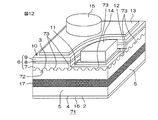
図12は、本発明の第8実施形態に係る半導体発光素子71の斜視図である。図12において、前述の第1実施形態において述べた構成と同様の構成については同一の参照符号を付して説明を省略する。
図12を参照して、本実施形態に係る基板2の一方表面3には、その全域に亘って凹凸72が形成されており、これによって基板2がPSS(Patterned Sapphire Substrate)とされている。この凹凸72には、規則的に配列された複数個の凸部73が含まれている。複数個の凸部73は、行列状に配列されていてもよいし、千鳥状に配列されていてもよい。むろん、複数個の凸部73は、規則性なく離散的に配列されていてもよい。PSSとされた基板2によれば、エピタキシャル層6(発光層8)で生成された光を光反射層16に加えて凹凸72によってエピタキシャル層6側に反射させることができるから、輝度を向上させることが可能となる。
<8th Embodiment>
FIG. 12 is a perspective view of the semiconductor light emitting device 71 according to the eighth embodiment of the present invention. In FIG. 12, the same reference numerals are given to the same configurations as those described in the first embodiment described above, and the description thereof will be omitted.
With reference to FIG. 12, unevenness 72 is formed on one surface 3 of the substrate 2 according to the present embodiment over the entire area thereof, whereby the substrate 2 is designated as PSS (Patterned Sapphire Substrate). The unevenness 72 includes a plurality of regularly arranged convex portions 73. The plurality of convex portions 73 may be arranged in a matrix or in a staggered manner. Of course, the plurality of convex portions 73 may be arranged discretely without regularity. According to the substrate 2 as PSS, the light generated by the epitaxial layer 6 (light emitting layer 8) can be reflected to the epitaxial layer 6 side by the unevenness 72 in addition to the light reflecting layer 16, so that the brightness is improved. It becomes possible.

このようなPSSとされた基板2は、前述のウエハ42準備工程(図4のステップS1)の後、エピタキシャル層形成工程(図4のステップS2)に先立って、たとえばマスクを介するエッチングによりウエハ42の一方表面43の一部を選択的に除去することによって形成できる。
一方表面43に凹凸72が形成されたウエハ42では、一方表面43側からレーザ光を照射すると当該レーザ光が凹凸72によって反射されるため、ウエハ42の内部に改質層17を良好に形成するのが困難となるという課題がある。これに対して、本実施形態に係る半導体発光素子71の製造方法によれば、改質層形成工程(図4のステップS7)において、ウエハ42の他方表面44側からレーザ光を照射しているから、ウエハ42の一方表面43に形成された凹凸72が改質層17を形成する上で弊害となることはない。また、ウエハ42の一方表面43に形成された凹凸72がレーザ光によって変質するのも効果的に抑制できる。
The substrate 2 as such a PSS is subjected to, for example, etching through a mask after the wafer 42 preparation step (step S1 in FIG. 4) and prior to the epitaxial layer forming step (step S2 in FIG. 4). It can be formed by selectively removing a part of one surface 43.
On the other hand, in the wafer 42 having the unevenness 72 formed on the surface 43, when the laser beam is irradiated from the surface 43 side, the laser beam is reflected by the unevenness 72, so that the modified layer 17 is satisfactorily formed inside the wafer 42. There is a problem that it becomes difficult. On the other hand, according to the method for manufacturing the semiconductor light emitting device 71 according to the present embodiment, in the modified layer forming step (step S7 in FIG. 4), the laser beam is irradiated from the other surface 44 side of the wafer 42. Therefore, the unevenness 72 formed on one surface 43 of the wafer 42 does not hinder the formation of the modified layer 17. Further, it is possible to effectively suppress that the unevenness 72 formed on one surface 43 of the wafer 42 is altered by the laser beam.

これにより、基板2の他方表面4の全域が光反射層16によって良好に被覆されていると共に、基板2の一方表面3に凹凸72が良好に形成された構成を得ることができるから、輝度を効果的に向上させることのできる半導体発光素子71を製造し、提供できる。
なお、本実施形態では、基板2の一方表面3に、当該基板2を利用して凹凸72が形成された例について説明したが、凹凸72は、基板2と異なる材料によって形成されていてもよい。たとえば、凹凸72は、基板2の一方表面3に絶縁膜を成膜した後、当該絶縁膜を凹凸状に選択的にパターニングすることによって形成されたものであってもよい。凹凸72に含まれる凹部は、基板2の一方表面3を露出させるように形成されていてもよい。凹凸72を形成する絶縁膜は、たとえばZrO、Al、SiO、TiO、Ta、Nb、AlN、SiN、AlONおよびSiONを含む群から選択される1種以上の絶縁材料種を含んでいてもよい。
As a result, the entire area of the other surface 4 of the substrate 2 is well covered by the light reflecting layer 16, and the unevenness 72 is well formed on one surface 3 of the substrate 2, so that the brightness can be increased. A semiconductor light emitting device 71 that can be effectively improved can be manufactured and provided.
In the present embodiment, an example in which the unevenness 72 is formed on one surface 3 of the substrate 2 by using the substrate 2 has been described, but the unevenness 72 may be formed of a material different from that of the substrate 2. .. For example, the unevenness 72 may be formed by forming an insulating film on one surface 3 of the substrate 2 and then selectively patterning the insulating film in an uneven shape. The concave portion included in the unevenness 72 may be formed so as to expose one surface 3 of the substrate 2. The insulating film forming the unevenness 72 is one selected from the group including, for example, ZrO 2 , Al 2 O 3 , SiO 2 , TiO 2 , Ta 2 O 5 , Nb 2 O 5 , AlN, SiN, AlON and SiON. The above insulating material types may be included.

基板2の一方表面3に凹凸72(凸部73)が形成された構成は、第1実施形態の構成に限らず、前述の第2実施形態〜第7実施形態にも適用できる。
以上、本発明の実施形態について説明したが、本発明はさらに他の形態で実施することもできる。
たとえば、前述の各実施形態において、各半導体部分の導電型が反転された構成が採用されてもよい。つまり、p型の部分がn型とされ、n型の部分がp型とされてもよい。したがって、基板2の一方表面3上にこの順に積層されたp型の第1半導体層7、発光層8およびn型の第2半導体層9を含むエピタキシャル層6が形成されてもよい。
The configuration in which the unevenness 72 (convex portion 73) is formed on one surface 3 of the substrate 2 is not limited to the configuration of the first embodiment, and can be applied to the above-mentioned second to seventh embodiments.
Although the embodiments of the present invention have been described above, the present invention can also be implemented in other embodiments.
For example, in each of the above-described embodiments, a configuration in which the conductive type of each semiconductor portion is inverted may be adopted. That is, the p-type portion may be n-type and the n-type portion may be p-type. Therefore, an epitaxial layer 6 including a p-type first semiconductor layer 7, a light emitting layer 8 and an n-type second semiconductor layer 9 laminated in this order on one surface 3 of the substrate 2 may be formed.

また、前述の各実施形態では、第1外部端子14と第2外部端子15とが基板2の一つの対角線に沿って互いに間隔を空けて配置された例について説明した。しかし、第1外部端子14および第2外部端子15は、平面視において基板2の一つの辺が延びる方向に沿って互いに間隔を空けて配置されていてもよい。
その他、特許請求の範囲に記載された事項の範囲で種々の設計変更を施すことが可能である。
Further, in each of the above-described embodiments, an example in which the first external terminal 14 and the second external terminal 15 are arranged at intervals along one diagonal line of the substrate 2 has been described. However, the first external terminal 14 and the second external terminal 15 may be arranged at intervals from each other along the direction in which one side of the substrate 2 extends in a plan view.
In addition, various design changes can be made within the scope of the matters described in the claims.

1,51,54,57,60,63,67,71…半導体発光素子、2…基板、3…基板の一方表面、4…基板の他方表面、5…基板の側面、6…エピタキシャル層(半導体層)、7…第1半導体層、8…発光層、9…第2半導体層、10…メサ構造、16…光反射層、17…改質層、42…ウエハ、43…ウエハの一方表面、44…ウエハの他方表面、45…素子形成領域、52,55,58,61,64,68…第1改質層、53,56,59,62,65,69…第2改質層、66,70…中間改質層 1,51,54,57,60,63,67,71 ... semiconductor light emitting device, 2 ... substrate, 3 ... one surface of substrate, 4 ... other surface of substrate, 5 ... side surface of substrate, 6 ... epitaxial layer (semiconductor) Layer), 7 ... 1st semiconductor layer, 8 ... light emitting layer, 9 ... second semiconductor layer, 10 ... mesa structure, 16 ... light reflecting layer, 17 ... modified layer, 42 ... wafer, 43 ... one surface of wafer, 44 ... the other surface of the wafer, 45 ... element forming region, 52, 55, 58, 61, 64, 68 ... first modified layer, 53, 56, 59, 62, 65, 69 ... second modified layer, 66. , 70 ... Intermediate modified layer

Claims (31)

一方側の第1主面、他方側の第2主面、ならびに、前記第1主面および前記第2主面をそれぞれ接続する第1側面、第2側面、第3側面および第4側面を有する基板と、
前記基板の前記第1主面の上に形成され、光が生成される半導体層と、
前記基板の前記第2主面の全域を被覆し、前記半導体層で生成された光を前記半導体層に向けて反射させる光反射層と、
前記基板において、前記第2主面、前記第1側面、前記第2側面、前記第3側面および前記第4側面からそれぞれ露出し、かつ、前記半導体層を露出させるように前記第1主面から前記第2主面側に間隔を空けて前記第1側面、前記第2側面、前記第3側面および前記第4側面にそれぞれ形成され、前記基板を構成する材料が変質することによって他の領域の結晶強度よりも小さい結晶強度とされた改質層と、を含む、半導体発光素子。
It has a first main surface on one side, a second main surface on the other side, and a first side surface, a second side surface, a third side surface, and a fourth side surface connecting the first main surface and the second main surface, respectively. With the board
A semiconductor layer formed on the first main surface of the substrate to generate light, and
A light reflecting layer that covers the entire area of the second main surface of the substrate and reflects the light generated by the semiconductor layer toward the semiconductor layer.
In the substrate, from the first main surface so as to be exposed from the second main surface, the first side surface, the second side surface, the third side surface, and the fourth side surface, respectively, and to expose the semiconductor layer. the first side surface at intervals in the second main surface side, the second side surface, are formed respectively on the third side and the fourth side surface, the other I by the fact that the material constituting the substrate is altered A semiconductor light emitting device including a modified layer having a crystal strength smaller than the crystal strength in the region of .
前記光反射層は、一様な材質で前記基板の前記第2主面を被覆している、請求項1に記載の半導体発光素子。 The semiconductor light emitting device according to claim 1, wherein the light reflecting layer is made of a uniform material and covers the second main surface of the substrate. 前記改質層は、前記基板の厚さ方向に関して、前記光反射層に対向している、請求項1または2に記載の半導体発光素子。 The semiconductor light emitting device according to claim 1 or 2, wherein the modified layer faces the light reflecting layer in the thickness direction of the substrate. 前記半導体層は、一様な材質で前記基板の前記第1主面の上に形成されている、請求項1〜3のいずれか一項に記載の半導体発光素子。 The semiconductor light emitting device according to any one of claims 1 to 3, wherein the semiconductor layer is made of a uniform material and is formed on the first main surface of the substrate. 前記半導体層は、前記基板の前記第1主面の全域を被覆している、請求項1〜4のいずれか一項に記載の半導体発光素子。 The semiconductor light emitting device according to any one of claims 1 to 4, wherein the semiconductor layer covers the entire area of the first main surface of the substrate. 前記半導体層は、前記基板の前記第1主面側からこの順に積層された第1導電型の第1半導体層、発光層および第2導電型の第2半導体層を含む、請求項1〜5のいずれか一項に記載の半導体発光素子。 Claims 1 to 5 include the semiconductor layer including a first conductive type first semiconductor layer, a light emitting layer, and a second conductive type second semiconductor layer laminated in this order from the first main surface side of the substrate. The semiconductor light emitting device according to any one of the above. 前記第1半導体層は、外部に露出した第1露出部を含み、
前記第2半導体層は、外部に露出した第2露出部を含む、請求項6に記載の半導体発光素子。
The first semiconductor layer includes a first exposed portion exposed to the outside, and includes a first exposed portion.
The semiconductor light emitting device according to claim 6, wherein the second semiconductor layer includes a second exposed portion exposed to the outside.
前記半導体層は、前記第1半導体層を露出させるように、前記第1半導体層の一部、前記発光層および前記第2半導体層を選択的に切り欠いて形成されたメサ構造を含み、
前記第1半導体層の前記第1露出部は、前記メサ構造外の領域に形成され、
前記第2半導体層の前記第2露出部は、前記メサ構造に形成されている、請求項7に記載の半導体発光素子。
The semiconductor layer includes a part of the first semiconductor layer, a light emitting layer, and a mesa structure formed by selectively cutting out the second semiconductor layer so as to expose the first semiconductor layer.
The first exposed portion of the first semiconductor layer is formed in a region outside the mesa structure.
The semiconductor light emitting device according to claim 7, wherein the second exposed portion of the second semiconductor layer is formed in the mesa structure.
前記第1半導体層の前記第1露出部の上に形成され、前記第1半導体層に電気的に接続された第1コンタクト電極をさらに含む、請求項7または8に記載の半導体発光素子。 The semiconductor light emitting device according to claim 7 or 8, further comprising a first contact electrode formed on the first exposed portion of the first semiconductor layer and electrically connected to the first semiconductor layer. 前記第1コンタクト電極は、前記第1露出部の周縁から前記第1露出部の内方に間隔を空けて形成されている、請求項9に記載の半導体発光素子。 The semiconductor light emitting device according to claim 9, wherein the first contact electrode is formed at intervals from the peripheral edge of the first exposed portion to the inside of the first exposed portion. 前記第1コンタクト電極の上に形成され、前記第1コンタクト電極に電気的に接続された第1外部端子をさらに含む、請求項9または10に記載の半導体発光素子。 The semiconductor light emitting device according to claim 9 or 10, further comprising a first external terminal formed on the first contact electrode and electrically connected to the first contact electrode. 前記第1外部端子は、平面視において前記第1コンタクト電極の周縁に取り囲まれた領域内に形成されている、請求項11に記載の半導体発光素子。 The semiconductor light emitting device according to claim 11, wherein the first external terminal is formed in a region surrounded by a peripheral edge of the first contact electrode in a plan view. 前記第2半導体層の前記第2露出部の上に形成され、前記第2半導体層に電気的に接続された第2コンタクト電極をさらに含む、請求項6〜12のいずれか一項に記載の半導体発光素子。 The second invention of any one of claims 6 to 12, further comprising a second contact electrode formed on the second exposed portion of the second semiconductor layer and electrically connected to the second semiconductor layer. Semiconductor light emitting element. 前記第2コンタクト電極は、平面視において前記第2露出部の周縁から前記第2露出部の内方に間隔を空けて前記第2半導体層の上に形成されている、請求項13に記載の半導体発光素子。 The thirteenth aspect of the present invention, wherein the second contact electrode is formed on the second semiconductor layer at a distance from the peripheral edge of the second exposed portion to the inside of the second exposed portion in a plan view. Semiconductor light emitting element. 前記第2コンタクト電極の上に形成され、前記第2コンタクト電極に電気的に接続された第2外部端子をさらに含む、請求項13または14に記載の半導体発光素子。 The semiconductor light emitting device according to claim 13 or 14, further comprising a second external terminal formed on the second contact electrode and electrically connected to the second contact electrode. 前記第2外部端子は、平面視において前記第2コンタクト電極の周縁に取り囲まれた領域内に形成されている、請求項15に記載の半導体発光素子。 The semiconductor light emitting device according to claim 15, wherein the second external terminal is formed in a region surrounded by a peripheral edge of the second contact electrode in a plan view. 前記改質層は、前記第1側面、前記第2側面、前記第3側面および前記第4側面に沿って帯状に形成されている、請求項1〜16のいずれか一項に記載の半導体発光素子。 The semiconductor light emitting device according to any one of claims 1 to 16, wherein the modified layer is formed in a band shape along the first side surface, the second side surface, the third side surface, and the fourth side surface. element. 前記改質層は、前記基板の前記第1主面と平行な方向に延びている、請求項1〜17のいずれか一項に記載の半導体発光素子。 The semiconductor light emitting device according to any one of claims 1 to 17, wherein the modified layer extends in a direction parallel to the first main surface of the substrate. 前記改質層は、前記基板の前記第1主面側に形成された第1改質層、および、前記第1改質層から間隔を空けて前記基板の前記第2主面側に形成された第2改質層を含む、請求項1〜18のいずれか一項に記載の半導体発光素子。 The modified layer is formed on the first modified layer formed on the first main surface side of the substrate and on the second main surface side of the substrate at intervals from the first modified layer. The semiconductor light emitting device according to any one of claims 1 to 18, which includes a second modified layer. 前記改質層は、前記基板の前記第1主面側に形成された第1改質層、および、前記第1改質層に重なるように前記基板の前記第2主面側に形成された第2改質層を含む、請求項1〜18のいずれか一項に記載の半導体発光素子。 The modified layer was formed on the first modified layer formed on the first main surface side of the substrate and on the second main surface side of the substrate so as to overlap the first modified layer. The semiconductor light emitting device according to any one of claims 1 to 18, which includes a second modified layer. 前記改質層は、前記基板の前記第1主面側に形成された第1改質層、前記第1改質層から間隔を空けて前記基板の前記第2主面側に形成された第2改質層、ならびに、前記第1改質層および前記第2改質層の間に形成された中間改質層を含む、請求項1〜18のいずれか一項に記載の半導体発光素子。 The modified layer is a first modified layer formed on the first main surface side of the substrate, and a second modified layer formed on the second main surface side of the substrate at intervals from the first modified layer. The semiconductor light emitting device according to any one of claims 1 to 18, further comprising a modified layer and an intermediate modified layer formed between the first modified layer and the second modified layer. 前記中間改質層は、前記基板の前記第1主面側において前記第1改質層と重なり、前記基板の前記第2主面側において前記第2改質層と重なるように形成されている、請求項21に記載の半導体発光素子。 The intermediate modified layer is formed so as to overlap the first modified layer on the first main surface side of the substrate and overlap the second modified layer on the second main surface side of the substrate. The semiconductor light emitting device according to claim 21. 前記改質層は、前記光反射層に接している、請求項1〜22のいずれか一項に記載の半導体発光素子。 The semiconductor light emitting device according to any one of claims 1 to 22 , wherein the modified layer is in contact with the light reflecting layer. 前記改質層は、前記基板の角部まで延びている、請求項1〜23のいずれか一項に記載の半導体発光素子。 The semiconductor light emitting device according to any one of claims 1 to 23 , wherein the modified layer extends to a corner portion of the substrate. 前記改質層は、前記基板の前記角部から露出している、請求項24に記載の半導体発光素子。 The semiconductor light emitting device according to claim 24 , wherein the modified layer is exposed from the corner portion of the substrate. 前記改質層は、前記半導体層の全域を露出させている、請求項1〜25のいずれか一項に記載の半導体発光素子。 The semiconductor light emitting device according to any one of claims 1 to 25 , wherein the modified layer exposes the entire entire surface of the semiconductor layer. 前記光反射層は、金属膜を含む、請求項1〜26のいずれか一項に記載の半導体発光素子。 The semiconductor light emitting device according to any one of claims 1 to 26 , wherein the light reflecting layer includes a metal film. 前記光反射層は、絶縁層を含む、請求項1〜27のいずれか一項に記載の半導体発光素子。 The semiconductor light emitting device according to any one of claims 1 to 27 , wherein the light reflecting layer includes an insulating layer. 前記絶縁層は、屈折率の異なる複数の絶縁膜が積層された積層構造を有している、請求項28に記載の半導体発光素子。 The semiconductor light emitting device according to claim 28 , wherein the insulating layer has a laminated structure in which a plurality of insulating films having different refractive indexes are laminated. 前記改質層は、前記第1主面から前記第2主面側に10μm以上の間隔を空けて前記第1側面、前記第2側面、前記第3側面および前記第4側面にそれぞれ形成されている、請求項1〜29のいずれか一項に記載の半導体発光素子。 The modified layer is formed on the first side surface, the second side surface, the third side surface, and the fourth side surface at intervals of 10 μm or more from the first main surface to the second main surface side, respectively. The semiconductor light emitting device according to any one of claims 1 to 29. 前記第2主面は、鏡面である、請求項1〜30のいずれか一項に記載の半導体発光素子。 The semiconductor light emitting device according to any one of claims 1 to 30, wherein the second main surface is a mirror surface.
JP2016111145A 2016-06-02 2016-06-02 Semiconductor light emitting device and its manufacturing method Active JP6789675B2 (en)

Priority Applications (2)

Application Number Priority Date Filing Date Title
JP2016111145A JP6789675B2 (en) 2016-06-02 2016-06-02 Semiconductor light emitting device and its manufacturing method
US15/610,983 US10497831B2 (en) 2016-06-02 2017-06-01 Semiconductor light emitting element and manufacturing method thereof

Applications Claiming Priority (1)

Application Number Priority Date Filing Date Title
JP2016111145A JP6789675B2 (en) 2016-06-02 2016-06-02 Semiconductor light emitting device and its manufacturing method

Publications (3)

Publication Number Publication Date
JP2017216423A JP2017216423A (en) 2017-12-07
JP2017216423A5 JP2017216423A5 (en) 2019-03-14
JP6789675B2 true JP6789675B2 (en) 2020-11-25

Family

ID=60483511

Family Applications (1)

Application Number Title Priority Date Filing Date
JP2016111145A Active JP6789675B2 (en) 2016-06-02 2016-06-02 Semiconductor light emitting device and its manufacturing method

Country Status (2)

Country Link
US (1) US10497831B2 (en)
JP (1) JP6789675B2 (en)

Families Citing this family (9)

* Cited by examiner, † Cited by third party
Publication number Priority date Publication date Assignee Title
US10388526B1 (en) 2018-04-20 2019-08-20 Semiconductor Components Industries, Llc Semiconductor wafer thinning systems and related methods
US10896815B2 (en) 2018-05-22 2021-01-19 Semiconductor Components Industries, Llc Semiconductor substrate singulation systems and related methods
US11121035B2 (en) 2018-05-22 2021-09-14 Semiconductor Components Industries, Llc Semiconductor substrate processing methods
US20190363018A1 (en) 2018-05-24 2019-11-28 Semiconductor Components Industries, Llc Die cleaning systems and related methods
US11830771B2 (en) 2018-05-31 2023-11-28 Semiconductor Components Industries, Llc Semiconductor substrate production systems and related methods
US10468304B1 (en) 2018-05-31 2019-11-05 Semiconductor Components Industries, Llc Semiconductor substrate production systems and related methods
DE102019201438B4 (en) * 2019-02-05 2024-05-02 Disco Corporation Method for producing a substrate and system for producing a substrate
KR102511747B1 (en) * 2021-07-16 2023-03-20 주식회사 글로벌테크놀로지 Led package, semiconductor chip mounted on the led package and method for fabricating the same
WO2024024272A1 (en) * 2022-07-26 2024-02-01 ソニーグループ株式会社 Light-emitting device

Family Cites Families (18)

* Cited by examiner, † Cited by third party
Publication number Priority date Publication date Assignee Title
JP3795007B2 (en) * 2002-11-27 2006-07-12 松下電器産業株式会社 Semiconductor light emitting device and manufacturing method thereof
US7223998B2 (en) * 2004-09-10 2007-05-29 The Regents Of The University Of California White, single or multi-color light emitting diodes by recycling guided modes
US7932111B2 (en) * 2005-02-23 2011-04-26 Cree, Inc. Substrate removal process for high light extraction LEDs
CN101218687B (en) * 2005-07-05 2012-07-04 昭和电工株式会社 Light-emitting diode and method for fabrication thereof
JP2007130768A (en) * 2005-11-08 2007-05-31 Seiko Epson Corp Cutting method of quartz substrate
JP2011243875A (en) * 2010-05-20 2011-12-01 Disco Abrasive Syst Ltd Dividing method of sapphire wafer
JP2013004741A (en) * 2011-06-16 2013-01-07 Toshiba Corp Semiconductor light-emitting element
JP2013042119A (en) * 2011-07-21 2013-02-28 Hamamatsu Photonics Kk Light-emitting element manufacturing method
JP5886603B2 (en) * 2011-11-11 2016-03-16 株式会社ディスコ Processing method of optical device wafer
JP5988600B2 (en) * 2012-02-10 2016-09-07 株式会社ディスコ Method for dividing sapphire wafer
JP6199281B2 (en) * 2012-03-23 2017-09-20 シャープ株式会社 Semiconductor light emitting device, method for manufacturing semiconductor light emitting device, semiconductor light emitting device, and substrate
TWI581451B (en) * 2012-05-21 2017-05-01 晶元光電股份有限公司 Optoelectronic device and method for manufacturing the same
JP2014017283A (en) * 2012-07-05 2014-01-30 Sharp Corp Method of manufacturing nitride compound semiconductor light-emitting element
JP6047989B2 (en) * 2012-08-07 2016-12-21 日亜化学工業株式会社 Semiconductor light emitting device and manufacturing method thereof
JP6034097B2 (en) * 2012-08-28 2016-11-30 株式会社ディスコ Laser processing equipment
JP6040769B2 (en) * 2012-12-28 2016-12-07 日亜化学工業株式会社 Light emitting device and manufacturing method thereof
JP6187156B2 (en) * 2013-10-29 2017-08-30 日亜化学工業株式会社 Method of manufacturing nitride semiconductor device
KR102357289B1 (en) * 2014-07-01 2022-02-03 서울바이오시스 주식회사 Light emitting device

Also Published As

Publication number Publication date
US10497831B2 (en) 2019-12-03
US20170352781A1 (en) 2017-12-07
JP2017216423A (en) 2017-12-07

Similar Documents

Publication Publication Date Title
JP6789675B2 (en) Semiconductor light emitting device and its manufacturing method
JP7248934B2 (en) light emitting device
US9905741B2 (en) Light emitting device and manufacturing method thereof
JP5421001B2 (en) Light emitting device and manufacturing method thereof
CN111129255B (en) Light emitting diode
JP5508244B2 (en) Manufacturing method of semiconductor light emitting device
US9484498B2 (en) Light emitting structure having electrodes forming a concave surface and manufacturing method thereof
JP2020141153A (en) Method of manufacturing light emitting element
US9799808B2 (en) Light emitting element and light emitting element package
TWI517459B (en) Semiconductor light emitting device and method for manufacturing same
JP6261718B2 (en) Light emitting semiconductor device and method for manufacturing light emitting semiconductor device
JP2016039324A (en) Light-emitting device and method for manufacturing light-emitting device
CN109449754B (en) Vertical cavity surface emitting laser and manufacturing method thereof
US10804424B2 (en) Method for manufacturing light emitting element
US9947834B2 (en) Light emitting element and light emitting element package
US20240063357A1 (en) Light emitting diode, light emitting diode module, and display device including the same
TWI807028B (en) Light emitting element and its manufacturing method
KR20180097979A (en) Light emitting diode having light blocking layer
JP6508189B2 (en) Light emitting device
KR20150018481A (en) Semiconductor light emitting device and manufacturing method of the same
JP7007561B2 (en) Light emitting device and its manufacturing method
US8803179B2 (en) Semiconductor light emitting device
JP2017038024A (en) Semiconductor light-emitting element, method for manufacturing the same, light-emitting element package including light-emitting element, and light-emitting device
JP6269901B1 (en) Light emitting device
KR101629403B1 (en) Semiconductor light emitting device and manufacturing method of the same

Legal Events

Date Code Title Description
A521 Request for written amendment filed

Free format text: JAPANESE INTERMEDIATE CODE: A523

Effective date: 20190130

A621 Written request for application examination

Free format text: JAPANESE INTERMEDIATE CODE: A621

Effective date: 20190521

A977 Report on retrieval

Free format text: JAPANESE INTERMEDIATE CODE: A971007

Effective date: 20200528

A131 Notification of reasons for refusal

Free format text: JAPANESE INTERMEDIATE CODE: A131

Effective date: 20200611

A521 Request for written amendment filed

Free format text: JAPANESE INTERMEDIATE CODE: A523

Effective date: 20200803

TRDD Decision of grant or rejection written
A01 Written decision to grant a patent or to grant a registration (utility model)

Free format text: JAPANESE INTERMEDIATE CODE: A01

Effective date: 20201029

A61 First payment of annual fees (during grant procedure)

Free format text: JAPANESE INTERMEDIATE CODE: A61

Effective date: 20201104

R150 Certificate of patent or registration of utility model

Ref document number: 6789675

Country of ref document: JP

Free format text: JAPANESE INTERMEDIATE CODE: R150

R250 Receipt of annual fees

Free format text: JAPANESE INTERMEDIATE CODE: R250