JP6787236B2 - Power converter - Google Patents
Power converter Download PDFInfo
- Publication number
- JP6787236B2 JP6787236B2 JP2017079343A JP2017079343A JP6787236B2 JP 6787236 B2 JP6787236 B2 JP 6787236B2 JP 2017079343 A JP2017079343 A JP 2017079343A JP 2017079343 A JP2017079343 A JP 2017079343A JP 6787236 B2 JP6787236 B2 JP 6787236B2
- Authority
- JP
- Japan
- Prior art keywords
- dead time
- current
- voltage
- power conversion
- command
- Prior art date
- Legal status (The legal status is an assumption and is not a legal conclusion. Google has not performed a legal analysis and makes no representation as to the accuracy of the status listed.)
- Active
Links
Images


Description
本発明は電力変換装置に関するものである。 The present invention relates to a power converter.
電圧指令値に基づくスイッチング素子の動作により電力の供給を行うインバータでは、電力変換手段を構成する2つのアームのスイッチング素子の同時導通による短絡破壊防止を目的とし、スイッチング素子を同時にオフ動作状態に制御する期間を設けている。この期間はデッドタイムと呼ばれているが、このデッドタイムによって、インバータの出力電圧には電圧指令値には無い歪みが生じ、電圧指令値に対する出力電圧の誤差により制御精度が劣化することがあった。 In an inverter that supplies power by operating a switching element based on a voltage command value, the switching elements are simultaneously controlled to the off operating state for the purpose of preventing short-circuit breakage due to simultaneous conduction of the switching elements of the two arms that make up the power conversion means. There is a period to do it. This period is called dead time, but this dead time causes distortion in the output voltage of the inverter that is not in the voltage command value, and the control accuracy may deteriorate due to the error of the output voltage with respect to the voltage command value. It was.
デッドタイムによるインバータの出力電圧誤差を補償するための方法として、短絡防止時間の影響を求め、出力電流と逆極性の電圧を電圧指令値に加算する方法がある。(例えば非特許文献1) As a method for compensating for the output voltage error of the inverter due to the dead time, there is a method of obtaining the influence of the short circuit prevention time and adding a voltage having the opposite polarity to the output current to the voltage command value. (For example, Non-Patent Document 1)
また、2つのスイッチング周波数で一定の直流電流を流すように電流制御を行い、2つのスイッチング周波数での電圧指令の差に基づいて、出力電圧誤差を補償するための補償値を求める方法がある。(例えば特許文献1) Further, there is a method in which current control is performed so that a constant DC current flows at two switching frequencies, and a compensation value for compensating for an output voltage error is obtained based on the difference between voltage commands at the two switching frequencies. (For example, Patent Document 1)
しかしながら非特許文献1に示された従来の方法では、電圧指令値に加算する逆極性の電圧は端子電圧波形が矩形波状に瞬時に変化することを想定して求められている。このためスイッチング素子の電圧スイッチング特性やそのバラツキにより実際に加算される逆極性の電圧は、想定した矩形波状とは異なる。この想定の電圧と実際に加算される電圧との差異は結果としてデッドタイム補償の誤差となり、補償精度が低下することがあった。
However, in the conventional method shown in
また、特許文献1に示された従来の方法では、2つのスイッチング周波数での電圧指令出力の差に基づいて、補償値を求めることで、ハードウェアの個々の特性によるバラツキを解消した補償を可能としている。しかしながら2つのスイッチング周波数には、スイッチング素子の性能や電流リプル等により設定可能な範囲の制約があり、2つのスイッチング周波数によって求められる電圧指令の差を大きく設定することができない。このためS/N比をあげることができず、補償精度が低下することがあった。
Further, in the conventional method shown in
本発明は、上述のような問題を解決するためになされたもので、電流リプルやノイズの影響を抑制して、デッドタイムによる出力電圧誤差の補償に必要な補償量を求めることができる電力変換装置を提供することを目的とする。 The present invention has been made to solve the above-mentioned problems, and is capable of suppressing the influence of current ripple and noise to obtain the compensation amount required for compensation of output voltage error due to dead time. The purpose is to provide the device.
本発明にかかる電力変換装置は、スイッチング素子を有し、電流を負荷に供給する電力変換部と、前記スイッチング素子をオフ状態とする保護期間であるデッドタイムの長さを決定するデッドタイムの長さ指令を出力するシーケンス管理部、および前記デッドタイムの長さ指令に基づいて前記デッドタイムを付加した前記スイッチング素子をオンおよびオフ動作させるスイッチング指令を出力するデッドタイム付加部、を有する制御部と、を備え、前記シーケンス管理部は、前記デッドタイムの長さ指令に基づいた前記スイッチング指令によって前記スイッチング素子がオンおよびオフ動作されたときの前記電力変換部から前記負荷へ供給される電流値または前記スイッチング指令を生成するための電圧指令値を用いて、前記電圧指令値を補償する補償量を求めるものである。 The power conversion device according to the present invention has a switching element, a power conversion unit that supplies a current to a load, and a dead time length that determines the length of a dead time, which is a protection period for turning off the switching element. A control unit having a sequence management unit that outputs a command and a dead time addition unit that outputs a switching command that turns on and off the switching element to which the dead time is added based on the dead time length command. The sequence management unit is provided with a current value supplied from the power conversion unit to the load when the switching element is turned on and off by the switching command based on the dead time length command. The voltage command value for generating the switching command is used to obtain the compensation amount for compensating the voltage command value.
本発明にかかる電力変換装置によれば、電流リプルやノイズの影響を抑制して、デッドタイムによる出力電圧誤差の補償に必要な補償量を求めることができる。 According to the power conversion device according to the present invention, it is possible to suppress the influence of current ripple and noise and obtain the compensation amount required for compensation of the output voltage error due to the dead time.
実施の形態1.
図1は、この発明を実施するための実施の形態1にかかる電力変換装置を適用した電力変換システムの構成図である。
FIG. 1 is a configuration diagram of a power conversion system to which the power conversion device according to the first embodiment for carrying out the present invention is applied.
図1に示す上記電力変換システム全体は、本実施の形態の電力変換装置100、直流電源1、電流センサ3とで構成される。また、説明の便宜上、図1には負荷4を記載している。電力変換装置100は、直流電力を交流電力に変換するインバータの機能を有し、入力電源である直流電源1から供給される直流電力を交流電力に変換して負荷4に供給する。電流センサ3は電力変換装置100から負荷4に供給される電流の値に基づき電流検出信号Ioutを出力する。本実施の形態では電流センサ3を電力変換装置100とは別に設ける構成としたが、電力変換装置100に内蔵する構成としてもよい。
The entire power conversion system shown in FIG. 1 includes a
本実施の形態における電力変換装置100は、電力変換部2と制御部6とで構成されている。
The
電力変換部2は、P側とN側との2つのスイッチング素子20、21で構成され、それらは直列接続されている。P側スイッチング素子20およびN側スイッチング素子21はそれぞれIGBT(Insulated gate bipolar transistor)201、211およびFWD(Freewheeling Diode)202、212によって構成されている。また、スイッチング回路の両端の端子は外部の直流電源1に接続され、2レベル単相ハーフブリッジ回路が構成されている。なお、P側スイッチング素子20およびN側スイッチング素子21は単にスイッチング素子とも記載する。
The
本実施の形態において、スイッチング素子としてIGBT201、211を用いているが、MOSFET(Metal−oxide−smiconductor field−effect transistor)など他のスイッチング素子を用いることもできる。また、2レベル単相ハーフブリッジ回路を例に説明するが、本発明の方式はレベル数や相数を問わず適用できる。説明の便宜上、直流電源1は図1に示したXの位置を基準電位とし、−Vdc/2[V]とVdc/2[V]を出力するものとする。
In the present embodiment, the IGBTs 201 and 211 are used as the switching elements, but other switching elements such as MOSFETs (Metal-oxide-smiconductor field-effect transistors) can also be used. Further, although a two-level single-phase half-bridge circuit will be described as an example, the method of the present invention can be applied regardless of the number of levels and the number of phases. For convenience of explanation, it is assumed that the
スイッチング素子20、21の切り替えと、付加するデッドタイムについて以下で説明する。本実施の形態の回路は、P側スイッチング素子20とN側スイッチング素子21とを相補的にオンおよびオフ動作させて上記スイッチング回路から負荷4に電力を供給するための出力端子の端子電圧を変化させる。本実施の形態では、後述する制御部6からのスイッチング指令Sw2*に基づいて、オンおよびオフ状態の割合を変えることで、平均的な上記端子電圧を変化させ負荷4へ電力を供給する。
The switching of the switching elements 20 and 21 and the dead time to be added will be described below. In the circuit of this embodiment, the P-side switching element 20 and the N-side switching element 21 are complementarily turned on and off to change the terminal voltage of the output terminal for supplying power from the switching circuit to the load 4. Let me. In the present embodiment, the average terminal voltage is changed and power is supplied to the load 4 by changing the ratio of the on and off states based on the switching command Sw2 * from the
P側およびN側スイッチング素子20、21は高速にオンおよびオフ状態が切り替わるものであるが、実際はP側およびN側スイッチング素子20、21の、オンおよびオフ状態が切り替わるまでにはある程度の時間を要する。そのため、切り替わるまでに要する時間を考慮せずにP側およびN側スイッチング素子20、21の制御をすると、P側スイッチング素子20とN側スイッチング素子21とが共にオンとなる状態が現れる。その結果、電気的に短絡を生じ、回路に過大な電流が流れ回路が破損する。 The P-side and N-side switching elements 20 and 21 switch between the on and off states at high speed, but in reality, it takes a certain amount of time for the P-side and N-side switching elements 20 and 21 to switch between the on and off states. It takes. Therefore, if the P-side and N-side switching elements 20 and 21 are controlled without considering the time required for switching, a state in which both the P-side switching element 20 and the N-side switching element 21 are turned on appears. As a result, an electrical short circuit occurs, an excessive current flows through the circuit, and the circuit is damaged.
そこで、スイッチング指令Sw2*には、短絡を防止するためのデッドタイムと呼ばれる保護期間が設けられている。このデッドタイムの間は、相補的なオンおよびオフ状態の入れ替わりのタイミングで、P側およびN側スイッチング素子20、21が共にオフ状態となる。また、スイッチング指令Sw2*のような信号はフォトカプラ等の絶縁素子を介するため伝達遅れが生じる事が多い。さらに、絶縁素子を含む信号伝達経路の回路素子の個体差のため伝達遅れもばらつく場合がある。これらの伝達遅れもP側およびN側スイッチング素子20、21の短絡を招く要因である。このため、スイッチング指令Sw2*には上述の伝達遅れも考慮したデッドタイムが設けられている。 Therefore, the switching command Sw2 * is provided with a protection period called a dead time to prevent a short circuit. During this dead time, the P-side and N-side switching elements 20 and 21 are both turned off at the timing of complementary on and off switching. Further, since a signal such as the switching command Sw2 * passes through an insulating element such as a photocoupler, a transmission delay often occurs. Further, the transmission delay may vary due to individual differences in the circuit elements of the signal transmission path including the insulating element. These transmission delays are also factors that cause short circuits of the P-side and N-side switching elements 20 and 21. Therefore, the switching command Sw2 * is provided with a dead time in consideration of the above-mentioned transmission delay.
制御部6は、電流センサ3からの電流検出信号Ioutを入力とし、スイッチング指令Sw2*を出力とする。図2は制御部6のハード構成を示した図である。制御部6は、プロセッサ601と記憶装置602で構成され、後述する各部の機能はこれらにより実現可能である。例えば、記憶装置602には、制御用プログラムの他、後述する電圧指令値Vi*、電流指令値I*、デッドタイムの長さ指令Td*などの演算により得られたデータが保存格納されている。また、その処理の過程で一時的に記憶すべき情報等のデータが保存格納されている。
The
プロセッサ601は、記憶装置602に格納されているプログラムを読み出し実行する。また、本実施の形態の動作を実行する過程で一時的に記憶すべき情報の書き込みや読み出しを行う。
The
記憶装置602は、ランダムアクセスメモリ等の揮発性記憶装置と、フラッシュメモリ等の不揮発性の補助記憶装置とを具備している。また、不揮発性の補助記憶装置として、フラッシュメモリの代わりにハードディスク等の補助記憶装置を具備していてもよい。
The
図1のシステム構成図にて制御部6を説明する。制御部6はシーケンス管理部61、電圧指令生成部62、PWM処理部63、デッドタイム付加部(以下Td付加部と記載する)64で構成される。
The
シーケンス管理部61は電流指令値I*を電圧指令生成部62へ出力する。また、Td付加部64へデッドタイムの長さ指令Td*を出力する。
The
電圧指令生成部62はシーケンス管理部61からの電流指令値I*と電流センサ3からの電流検出信号Ioutとを用いて電流制御処理を行い、後述するPWM処理部63に電圧指令値Vi*を出力する。電流制御処理は例えば電流指令値I*と電流検出信号Ioutとの偏差が零となるように、電圧指令値Vi*を生成する。
The voltage
PWM処理部63は電圧指令生成部62からの電圧指令値Vi*に対し、例えば電圧指令値Vi*を直流電源電圧値Vdc/2[V]で除算し変調率指令に変換する。そして、三角波やノコギリ波との大小比較によるPWM処理を実施しスイッチング指令Sw1*を出力する。
The
Td付加部64はシーケンス管理部61からのデッドタイムの長さ指令Td*に従ってスイッチング指令Sw1*にデッドタイムを付加する。そしてデッドタイムを付加したスイッチング指令Sw2*を電力変換部2へ出力する。
The
ここでデッドタイムによって生じる誤差について分析する。付加されたデッドタイムの間では、スイッチング素子20、21を構成するIGBT201、211とFWD202、212のうち、IGBT201、211はオフ状態となる。このため、FWD202、212を電力変換部2の出力電流の少なくとも一部が通過する。上記出力電流は、電力変換部2の極性に基づいて、P側のFWD202またはN側のFWD212のどちらを通過するかが決定される。
Here, the error caused by the dead time is analyzed. During the added dead time, the IGBTs 201 and 211 of the IGBTs 201 and 211 and the
例えば、電力変換部2の出力電流の極性の方向が図1における上記出力端子から負荷4に向かう方向dと一致する場合を正とする。このとき、出力電流の極性の方向が正の場合は、N側のFWD212を出力電流が通過し、このN側FWD212を通じて電力変換部2の上記出力端子の電圧は−Vdc/2[V]になる。出力電流の極性の方向が負の場合は、P側のFWD202を電流が通過し、このP側のFWD202を通じて電力変換部2の出力電圧はVdc/2[V]となる。
For example, the case where the direction of the polarity of the output current of the
デッドタイムの間の電力変換部2の出力電圧誤差は、スイッチング素子20、21のスイッチング動作の近傍、例えば数[μsec]で、極短時間のパルス状に発生する。上述のようにスイッチング指令Sw2*は、PWM処理部63においてPWM処理を経て得られたスイッチング指令Sw1*にデッドタイムを付加したものである。このため該キャリアを基準として、パルス状の出力電圧誤差を該キャリア1周期区間内での平均値に換算すると(1)式に表すことができる。この(1)式で示した出力電圧誤差を、以下デッドタイム電圧誤差と記載する。
The output voltage error of the

(1)式中のVtdはデッドタイム電圧誤差、fcはキャリア周波数[Hz]、Tdは付加
するデッドタイムの長さ[sec]、Vdcは電力変換部2の入力となる直流リンク電圧、sign(i)は上記出力電流の極性をそれぞれ示している。付加するデッドタイムの長さは矩形波で理想的に付加されることを想定したものである。また、上記出力電流の極性は電力変換部2から負荷4に向かう方向dと一致する場合を正とし、正のとき1、負のとき−1とする。
In the equation (1), Vtd is the dead time voltage error, fc is the carrier frequency [Hz], Td is the length of the dead time to be added [sec], Vdc is the DC link voltage that is the input of the
デッドタイム電圧誤差を補償する方法としては、デッドタイム電圧誤差と逆極性の電圧を電圧指令値に加算することが一般的に実施されている。この電圧の補償制御をデッドタイム補償と言う。 As a method of compensating for the dead time voltage error, it is generally practiced to add a voltage having the opposite polarity to the dead time voltage error to the voltage command value. This voltage compensation control is called dead time compensation.
デッドタイム補償は概ね良好に動作するが、次に記載する複数の理由により補償精度が低下することがある。 Dead time compensation works generally well, but compensation accuracy may be reduced for several reasons:
補償精度が低下する第一の理由は電力変換部2の上記出力端子の端子電圧波形が理想のステップ波形とはならないためである。上述したようにスイッチング素子20、21のオンおよびオフ状態が切り替わるまでにはある程度の時間を要する。(1)式のデッドタイム電圧誤差は上記端子電圧がステップ波形に瞬時に変化する理想波形を想定して求められている。このため、理想波形との差異は結果としてデッドタイム補償の誤差となる。さらに上記端子電圧波形は電力変換部2の上記出力電流に応じて形状が変化する。この端子電圧の波形の変化もデッドタイム補償の誤差をもたらすことになる。
The first reason for the decrease in compensation accuracy is that the terminal voltage waveform of the output terminal of the
補償精度が低下する第二の理由は制御部6からスイッチング素子20、21へ生成されるスイッチング指令Sw2*の伝達遅れのバラつきによるものである。スイッチング指令Sw2*はデッドタイムの長さが矩形波なることを想定して生成されている。このため、スイッチング指令Sw2*の伝達遅れのバラつきは、想定されたデッドタイムの長さと実際のデッドタイムの長さの差異を生じさせる。よってデッドタイム補償の誤差をもたらすことになる。
The second reason why the compensation accuracy is lowered is that the transmission delay of the switching command Sw2 * generated from the
補償精度が低下する第三の理由はスイッチング素子20、21の過電圧保護に設置されるスイッチング素子を20、21構成するFWD201、211に並列された図示しないスナバ回路内のコンデンサの充放電によるものである。スナバ回路内のコンデンサの充放電により、デッドタイム中の上記端子電圧波形の形状が変化する。これもデッドタイム補償の誤差となる。電流による充放電動作であるため、負荷4の電流はもとより、実際に付加されるデッドタイムの長さによって上記端子電圧波形の形状の変化が発生する。 The third reason for the decrease in compensation accuracy is the charging and discharging of capacitors in the snubber circuit (not shown) parallel to the FWD 201 and 211 that configure the switching elements 20 and 21 installed in the overvoltage protection of the switching elements 20 and 21. is there. The shape of the terminal voltage waveform during the dead time changes due to the charging and discharging of the capacitor in the snubber circuit. This is also an error in dead time compensation. Since the charging / discharging operation is performed by a current, the shape of the terminal voltage waveform changes depending on not only the current of the load 4 but also the length of the dead time actually applied.
補償精度が低下する第四の理由はスナバ回路のコンデンサと同様にスイッチング素子20、21近傍に付随する浮遊容量の充放電が影響をもたらすためである。 The fourth reason for the decrease in compensation accuracy is that charging and discharging of stray capacitances in the vicinity of the switching elements 20 and 21 have an effect as in the case of the capacitor of the snubber circuit.
上述のように複数の要因で発生するデッドタイム電圧誤差は、(2)式にまとめて係数αとして表現することができる。この(2)式で示すデッドタイム電圧誤差に基づいて、逆極性の電圧値を電圧指令値に加算することで、高精度なデッドタイム補償を実現できる。言い換えると、高精度なデッドタイム補償の実現には、係数αを高い精度で入手する必要がある。そこで本実施の形態では、後述する動作を行うことで高精度な係数αの取得を実現する。 As described above, the dead time voltage error generated by a plurality of factors can be collectively expressed as a coefficient α in the equation (2). Highly accurate dead time compensation can be realized by adding a voltage value of opposite polarity to the voltage command value based on the dead time voltage error represented by the equation (2). In other words, in order to realize highly accurate dead time compensation, it is necessary to obtain the coefficient α with high accuracy. Therefore, in the present embodiment, the acquisition of the coefficient α with high accuracy is realized by performing the operation described later.
本実施の形態にかかる動作を説明する。図3は本実施の形態にかかる制御部6の実行動作の一例を示すフローチャート図である。本発明ではデッドタイムの長さを複数設定して電力変換制御を実施する。このとき負荷4の電流制御を行い、前記のデッドタイム長さに対応した電圧指令Vi*を記録する。ここで(1)式の逆極性の電圧を電圧指令Vi*に加算する一般的なデッドタイム補償をオフにしていると前記電圧指令Vi*には(2)式で示すデッドタイム電圧誤差を含む結果となる。デッドタイム長さTdとキャリア周波数fcは既知の値であり、直流リンク電圧Vdcは測定にて取得できるとする。この場合、前記(2)式に基づき、各デッドタイムの長さに対応する各電圧指令の傾きを求めることで(2)式の係数αを求めることができる。本実施の形態ではデッドタイムの長さを2種類設定する場合の構成を記載しており、図3のフローチャートはこれに対応する。前記傾きの計算は2種類のデッドタイム長さに対応した2種類の電圧指令の差分に基づいて計算できる。
The operation related to the present embodiment will be described. FIG. 3 is a flowchart showing an example of the execution operation of the
電流指令ステップS101では、シーケンス管理部61から電圧指令生成部62へ電流指令値I*を出力する。このときの電流指令値I*は任意に設定された値とする。電圧指令生成部62は、電流指令値I*と電流センサ3からの電流検出信号Ioutとに基づいて、上述した電流制御処理を行う。そして、電圧指令値Vi*をPWM処理部63に出力する。さらにPWM処理部63は、電圧指令生成部62からの電圧指令値Vi*に基づき、スイッチング指令Sw1*をTd付加部64へ生成する。
In the current command step S101, the current command value I * is output from the
第一のデッドタイムの長さ指令ステップS102では、シーケンス管理部61からTd付加部64へデッドタイムの長さ指令Td*を出力する。本実施の形態においては、デッドタイムの長さ指令Td*のある値としてTd1*を出力する。Td付加部64は、デッドタイム長さの指令Td1*に基づいてスイッチング指令Sw1*にデッドタイムを付加する。そして、デッドタイム付加後のスイッチング指令Sw2*を電力変換部2へ出力する。
In the first dead time length command step S102, the dead time length command Td * is output from the
ここまでのステップの動作により、電力変換部2ではスイッチング指令Sw2*に基づいてスイッチング素子20、21がオンおよびオフ動作される。電力変換部2は、スイッチング素子20、21のオンおよびオフ動作により、直流電源1から供給された電力を負荷4に出力する。
By the operation of the steps up to this point, the
このときの電力変換部2から負荷4へ供給される電流は、電力変換部2と負荷4とを接続する導線に設置された電流センサ3によって検出される。電流センサ3は、電流検出信号Ioutを電圧指令生成部62へ出力する。
The current supplied from the
第一の電圧指令取得ステップS103では、電圧指令値Vi*をV1*として記憶装置602に記憶する。電圧指令値V1*は、デッドタイムの長さ指令Td1*に基づいて上述した電流制御処理により新たに出力された電圧指令値である。
In the first voltage command acquisition step S103, the voltage command value Vi * is stored in the
電圧指令値V1*は、上述のように電圧指令生成部62にて電流指令値I*と電流検出信号Ioutとに基づいて生成される。このとき、デッドタイム補償は行われていないため、電流制御処理によって補償された結果、負荷4のインピーダンスによる電圧降下分とデッドタイム電圧誤差成分がシーケンス管理部61へ入力される電圧指令値V1*に含まれる。
The voltage command value V1 * is generated by the voltage
第二のデッドタイムの長さ指令ステップS104では、シーケンス管理部61からTd付加部64へデッドタイムの長さ指令Td2*を出力する。デッドタイムの長さ指令Td2*はデッドタイムの長さ指令Td1*とは異なる値である。Td付加部64は、デッドタイム長さの指令Td2*に基づいてスイッチング指令Sw1*にデッドタイムを付加する。そして、デッドタイム付加後のスイッチング指令Sw2*を電力変換部2へ出力する。
In the second dead time length command step S104, the dead time length command Td2 * is output from the
電力変換部2のスイッチング素子20、21はスイッチング指令Sw2*に基づいてオンおよびオフ動作される。電力変換部2はスイッチング素子20、21のオンおよびオフ動作により直流電源1から供給された直流電力を交流電力に変換し、負荷4に出力する。
The switching elements 20 and 21 of the
このときに電力変換部2から負荷4へ供給される電流が電力変換部2と負荷4とを接続する導線に設置された電流センサ3によって検出される。電流センサ3は、電流検出信号Ioutを電圧指令生成部62へ出力する。
At this time, the current supplied from the
第二の電圧指令取得ステップS105では、新たに取得した電圧指令値Vi*をV2*として記憶装置602に記憶する。電圧指令値V2*は、デッドタイムの長さ指令Td2*に基づいて上述した電流制御処理により新たに出力された電圧指令値である。
In the second voltage command acquisition step S105, the newly acquired voltage command value Vi * is stored in the
電圧指令値V2*は、上述のように電圧指令生成部62にて電流指令値I*と電流検出信号Ioutとに基づいて生成される。このとき、デッドタイム補償は行われていないため、電流制御処理によって補償された結果、負荷4のインピーダンスによる電圧降下分とデッドタイム電圧誤差成分がシーケンス管理部61へ入力される電圧指令値V2*に含まれる。
The voltage command value V2 * is generated by the voltage
係数α取得ステップS106では、記憶装置602に記憶された電圧指令値V1*、V2*に基づき、係数αを取得する。この動作は、プロセッサ601により、実行される。
In the coefficient α acquisition step S106, the coefficient α is acquired based on the voltage command values V1 * and V2 * stored in the
係数αの取得方法について説明する。上述のステップS101からS105の過程において得られる電圧指令値V1*およびV2*は、検出電流信号Ioutと電流指令値I*を用いた電流制御処理により生じる値である。この電圧指令値V1*およびV2*であるが、上述の(2)式に基づいてキャリア周波数fc[Hz]、デッドタイムの長さ指令[sec]、電力変換部2への入力となる直流リンク電圧Vdc、出力電流の極性sign(i)を用いて表すことができる。
The method of obtaining the coefficient α will be described. The voltage command values V1 * and V2 * obtained in the steps S101 to S105 described above are values generated by the current control process using the detected current signal Iout and the current command value I *. The voltage command values V1 * and V2 * are the carrier frequency fc [Hz], the dead time length command [sec], and the DC link that is input to the
(3)式は、デッドタイムの長さ指令をTd1*としたときに得られた電圧指令値V1*を(2)式に基づき表した式である。また、(4)式は、デッドタイムの長さ指令をTd2*としたときに得られた電圧指令値V2*を(2)式に基づいて表した式である。それぞれのZ・iは負荷4のインピーダンスによる電圧降下成分を示している。 Equation (3) is an equation expressing the voltage command value V1 * obtained when the dead time length command is Td1 * based on equation (2). Further, the equation (4) is an equation expressing the voltage command value V2 * obtained when the dead time length command is Td2 * based on the equation (2). Each Z · i shows a voltage drop component due to the impedance of the load 4.
係数α取得ステップS106では、まず、電圧指令値V1*の(3)式と電圧指令値V2*の(4)式との差分を計算する。すなわち、2つの電圧指令値V1*とV2*との差分を求めることにより(3)式と(4)式のそれぞれの右辺の負荷4のインピーダンスによる電圧降下成分Z・iを相殺し、電圧降下成分Z・iの影響をなくすことができる。また、(3)式および(4)式での記載は省略しているが、スイッチング素子20、21のオン電圧成分も同様に差分を計算することにより相殺できる。よって、デッドタイム電圧誤差のみを高精度に取り出すことができる。このとき、係数α以外は既知の値であるため、(5)式に示すように係数αを取得することができる。 In the coefficient α acquisition step S106, first, the difference between the equation (3) of the voltage command value V1 * and the equation (4) of the voltage command value V2 * is calculated. That is, by finding the difference between the two voltage command values V1 * and V2 *, the voltage drop components Z · i due to the impedance of the load 4 on the right side of each of the equations (3) and (4) are canceled out, and the voltage drop The influence of the components Z and i can be eliminated. Further, although the description in the equations (3) and (4) is omitted, the on-voltage components of the switching elements 20 and 21 can be offset by similarly calculating the difference. Therefore, only the dead time voltage error can be extracted with high accuracy. At this time, since the values other than the coefficient α are known values, the coefficient α can be obtained as shown in the equation (5).
このように、係数α取得ステップS106で係数αを取得すると、動作は終了される。以上が本実施の形態において係数αを求めるための基本的な実行動作である。これにより正確な係数αを取得することができる。なお、デッドタイムの長さ指令Td1*およびTd2*の値は任意で設定してよいが、設定可能な範囲内において、Td1*およびTd2*の値の差がより大きくなるように設定する方がよりよい。 In this way, when the coefficient α is acquired in the coefficient α acquisition step S106, the operation is terminated. The above is the basic execution operation for obtaining the coefficient α in the present embodiment. As a result, an accurate coefficient α can be obtained. The values of the dead time length commands Td1 * and Td2 * may be set arbitrarily, but it is better to set the difference between the values of Td1 * and Td2 * to be larger within the settable range. Better.
さらに、より正確なデッドタイム補償実現のため、図4に示すように電流指令変更ステップS107を設けてもよい。この場合、係数α取得ステップS106で係数αを取得した後、電流指令変更ステップS107で任意の電流指令I*に変更する。そして電流指令ステップS101で変更後の電流指令I*を出力し、上述したS101からS106の動作を繰り返す。図4はある任意の電流指令I*に対し2種類のデッドタイムの長さ指令にて測定を行うフローを示しているが、デッドタイムの長さ指令をTd1*とし、複数の電流指令I*に対して測定を行い、次にデッドタイムの長さ指令をTd2*とし、同様に複数のI*に対して測定を行う構成としてもよい。プロセッサ601の種類によっては、デッドタイムの長さ指令を変更する場合、プロセッサ601自体を停止・再起動させる必要がある機種がある。この場合、測定条件の変更に時間を要する場合があるが、前述の順序とすると、測定条件の変更に要する時間を削減することができる。計算に用いる電圧指令V1*およびV2*は記憶装置602に保存され、また前記電圧指令値が揃ってから(5)式の計算がなされるため本発明の本質的な効果には影響は与えない。
Further, in order to realize more accurate dead time compensation, the current command change step S107 may be provided as shown in FIG. In this case, after the coefficient α is acquired in the coefficient α acquisition step S106, the current command is changed to an arbitrary current command I * in the current command change step S107. Then, the changed current command I * is output in the current command step S101, and the operations of S101 to S106 described above are repeated. FIG. 4 shows a flow in which measurement is performed with two types of dead time length commands for an arbitrary current command I *. The dead time length command is Td1 *, and a plurality of current commands I * are used. Then, the dead time length command may be Td2 *, and the measurement may be performed on a plurality of I * in the same manner. Depending on the type of
これにより、電流指令値I*ごとの係数αを取得できる。すなわち、上記出力電流ごとのテーブルとして保持することができる。上記出力電流ごとに係数αをもつことにより、上記出力電流に応じてデッドタイム電圧の変化を考慮したデッドタイム補償が実施可能となる。さらに該デッドタイム補償により電力変換部2の出力電圧精度を向上させることができる。また、電力変換部2に付随する電流センサ3のみを用い、係数αの測定を自動で実施できるため、人手を介した測定と比較して労力を大幅に削減することが可能となる。
As a result, the coefficient α for each current command value I * can be obtained. That is, it can be held as a table for each output current. By having a coefficient α for each output current, it is possible to perform dead time compensation in consideration of a change in the dead time voltage according to the output current. Further, the dead time compensation can improve the output voltage accuracy of the
電流指令変更ステップS107では電流指令値I*は、一意的に増加または減少するように変更しステップS101からS106を繰り返すことで連続して変化する電流指令値I*ごとの係数αを取得してもよい。また、ランダムに変化させて各々の係数αを取得しテーブルを取得するようにしてもよい。繰り返し回数は、取得したいテーブルに応じて任意で決定してよい。テーブルを取得する場合の実行動作は、テーブルを取得した後、終了する。 In the current command change step S107, the current command value I * is changed so as to be uniquely increased or decreased, and by repeating steps S101 to S106, a coefficient α for each current command value I * that changes continuously is acquired. May be good. Further, it may be changed at random to acquire each coefficient α and acquire a table. The number of repetitions may be arbitrarily determined according to the table to be acquired. The execution operation when acquiring the table ends after acquiring the table.
図5は電圧指令値Vi*および電流指令値I*の関係を示すものであり、(3)式から(5)式を説明する図でもある。横軸は電流指令値I*、縦軸は電圧指令値Vi*とし、デッドタイムの長さ指令がTd1*のときに得られた電圧指令値V1*を各電流指令値I*ごとに◆でプロットしている。また、デッドタイムの長さ指令がTd2*のときも同様に電圧指令値V2*を電流指令値I*ごとに△でプロットしている。なお、図5では、説明の便宜上、直流通電した場合を示した例のみを示すが、交流通電などの他の通電方式に変更しても実効値で表すことにより同様の模式図を示すことが可能である。また、基本的な係数αの取得方法も同じである。 FIG. 5 shows the relationship between the voltage command value Vi * and the current command value I *, and is also a diagram illustrating equations (3) to (5). The horizontal axis is the current command value I *, the vertical axis is the voltage command value Vi *, and the voltage command value V1 * obtained when the dead time length command is Td1 * is indicated by ◆ for each current command value I *. I'm plotting. Further, when the dead time length command is Td2 *, the voltage command value V2 * is similarly plotted with Δ for each current command value I *. Note that, for convenience of explanation, FIG. 5 shows only an example showing the case where direct current is energized, but a similar schematic diagram can be shown by expressing the effective value even if the method is changed to another energization method such as alternating current energization. It is possible. The method for obtaining the basic coefficient α is also the same.
同じ電流指令値I*によって得られた電圧指令値V1*およびV2*にはそれぞれ同様の電圧降下成分Z・iが存在する。この電圧降下成分Z・iは、電流指令値I*ごとに得られた電圧指令値V1*とV2*との差分をとることにより、除去できる。その結果、図5の△と◆との間にあたる電圧の差分のみを得ることができる。そして、(5)式により、電圧指令値V1*とV2*との差分から係数αを求めることができることがわかる。 Similar voltage drop components Z and i exist in the voltage command values V1 * and V2 * obtained by the same current command value I *, respectively. This voltage drop component Z · i can be removed by taking the difference between the voltage command values V1 * and V2 * obtained for each current command value I *. As a result, only the difference in voltage between Δ and ◆ in FIG. 5 can be obtained. Then, it can be seen from the equation (5) that the coefficient α can be obtained from the difference between the voltage command values V1 * and V2 *.
また、直流電源1の種類によっては負荷4に電流を流すと、負荷4での電力消費によって、直流リンク電圧Vdcが変動する場合がある。例えば電源系統からの交流電力を整流して供給するダイオードコンバータなどが相当する。この時はデッドタイムの長さ指令Td*を変更した場合のそれぞれの直流リンク電圧値Vdcを記録して、(5)式に変えて(6)式を用いて係数αの計算を行ってもよい。なお図1においては該Vdcの検出箇所の記載は省略している。
Further, depending on the type of the
このように、本実施の形態では、デッドタイムの異なる2種類の電圧指令値V1*、V2*により、高精度に係数αを取得できる。また、求めた係数αを用いてデッドタイム補償を行うことで、補償精度の低下を抑制することができる。さらに、出力電流に応じた係数αのテーブルを取得しておくことで、出力電流に応じて選択した係数αをデッドタイム補償に用いることができ、より高精度な補償が可能となる。デッドタイム補償は、例えば、制御部6に図示しない補償部を設けた構成とし、補償部で上述したようなデッドタイム補償を実施することにより実現できる。
As described above, in the present embodiment, the coefficient α can be acquired with high accuracy by the two types of voltage command values V1 * and V2 * having different dead times. Further, by performing dead time compensation using the obtained coefficient α, it is possible to suppress a decrease in compensation accuracy. Further, by acquiring a table of the coefficient α corresponding to the output current, the coefficient α selected according to the output current can be used for dead time compensation, and more accurate compensation becomes possible. The dead time compensation can be realized, for example, by providing the
係数αの測定を、デッドタイムの長さを変更して行う利点についてさらに詳細に説明する。 The advantage of measuring the coefficient α by changing the length of the dead time will be described in more detail.
電力変換部2を用いて負荷4に電流を流す場合、PWM制御により、矩形波類似形状の電圧が負荷4に印加される。このため、電力変換部2からの上記出力電流には電流リプルが含まれる。この電流リプルによってαの測定精度が低下する場合がある。
When a current is passed through the load 4 by using the
上記αの測定精度低下の第一の理由は電流リプルによってサンプリングした電流とスイッチング近傍の電流の極性が異なることである。この電流リプルを避ける方法として、例えばPWM制御を行う際の比較に用いる搬送波が三角波キャリアの場合その山・谷タイミングなどの特定のタイミングで電流サンプリングを実施する方法がある。 The first reason for the decrease in measurement accuracy of α is that the polarities of the current sampled by the current ripple and the current near the switching are different. As a method of avoiding this current ripple, for example, when the carrier wave used for comparison when performing PWM control is a triangular wave carrier, there is a method of performing current sampling at a specific timing such as the peak / valley timing.
しかしながら、負荷4の電気時定数によっては、電流リプルが顕著となる。この結果、特に電流ゼロ近傍でスイッチング瞬間の電流値とサンプル電流値の大きさや極性が異なることがある。これは特に三角波キャリアのキャリア周波数を下げた場合に顕著である。 However, depending on the electrical time constant of the load 4, the current ripple becomes remarkable. As a result, the magnitude and polarity of the current value at the switching moment and the sample current value may differ, especially near zero current. This is particularly remarkable when the carrier frequency of the triangular wave carrier is lowered.
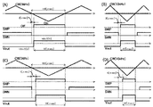
図6は電流サンプリングタイムとスイッチタイミングの関係を示している。これを用いてデッドタイム補償精度が低下する例を説明する。 FIG. 6 shows the relationship between the current sampling time and the switch timing. An example in which the dead time compensation accuracy is lowered will be described using this.
図6(A)は、横軸に時間をとり、低キャリア周波数で通電した場合の電流波形を示したものである。図6(B)は、横軸に時間をとり、高キャリア周波数で通電した場合の電流波形を示したものである。双方の電流波形中に○で記載のタイミングは三角波キャリアの頂点に同期した電流のサンプリングタイミングを示し、●で記載のタイミングはスイッチングタイミングを示している。 FIG. 6A shows a current waveform when energized at a low carrier frequency with time on the horizontal axis. FIG. 6B shows a current waveform when energized at a high carrier frequency with time on the horizontal axis. In both current waveforms, the timing marked with a circle indicates the sampling timing of the current synchronized with the apex of the triangular wave carrier, and the timing marked with ● indicates the switching timing.
図6中の電流波形の値の上下変動は、電流リプルが生じていることを表している。図6(A)、(B)双方の電流波形に電流リプルが生じているが、低キャリア周波数時(A)は、高キャリア周波数時(B)と比較し、電流リプルが大きいことがわかる。この大きな電流リプルによって例えば図6(A)の点線で囲った箇所のように、サンプリングした電流値とスイッチング近傍の電流値の極性が異なる場合がある。 The vertical fluctuation of the value of the current waveform in FIG. 6 indicates that the current ripple is occurring. Although current ripples occur in the current waveforms of both FIGS. 6A and 6B, it can be seen that the current ripples are larger at the low carrier frequency (A) than at the high carrier frequency (B). Due to this large current ripple, the polarities of the sampled current value and the current value in the vicinity of switching may differ, for example, as shown by the dotted line in FIG. 6 (A).
係数αの測定においては、電流制御系はPI制御器で構成されることが殆どである。すなわち、係数αの測定において、デッドタイム電圧誤差はPI制御器の積分器が受け持つことになる。このため、電流極性が異なる現象が発生すると、電流制御に大きな乱れが生じる。そしてこの乱れを含んだ電圧指令値Vi*が出力される。 In the measurement of the coefficient α, the current control system is mostly composed of a PI controller. That is, in the measurement of the coefficient α, the integrator of the PI controller is in charge of the dead time voltage error. Therefore, when a phenomenon in which the current polarities are different occurs, the current control is greatly disturbed. Then, the voltage command value Vi * including this disturbance is output.
この結果、上述の電圧指令値Vi*を用いる係数αの計算に誤差が生じる。この係数αに誤差が発生する現象は電流ゼロクロス近傍で顕著である。電流ゼロクロス近傍では特に、電流リプルが電流指令値Vi*に沿って負荷4に出力される出力電流である主電流に対して大きくなる。 As a result, an error occurs in the calculation of the coefficient α using the above-mentioned voltage command value Vi *. The phenomenon that an error occurs in this coefficient α is remarkable in the vicinity of the current zero cross. Especially in the vicinity of the current zero cross, the current ripple becomes larger than the main current, which is the output current output to the load 4 along the current command value Vi *.
上記αの測定精度低下の第二の理由は電流リプルが顕著になることによって、サンプリングした電流値と負荷4に流れる平均電流値との間に乖離が生じることによって発生する。この場合、2つのスイッチング周波数での電圧指令を用いる従来の方法では、負荷4での電圧降下がそれぞれ異なる。この差異が係数αの計算結果に流入し誤差を生じることがある。 The second reason for the decrease in the measurement accuracy of α is that the current ripple becomes remarkable and a discrepancy occurs between the sampled current value and the average current value flowing through the load 4. In this case, in the conventional method using the voltage command at the two switching frequencies, the voltage drop at the load 4 is different. This difference may flow into the calculation result of the coefficient α and cause an error.
図7(A)、(B)を用いてその例を説明する。図7(A)は横軸に時間をとり、負荷4の電気時定数よりもキャリア周波数の低い、低キャリア時の電流波形の例を示したものである。図7(B)は横軸に時間をとり、負荷4の電気時定数よりもキャリア周波数が高い、高キャリア時の電流波形の例を示したものである。双方の電流波形上に記載の○で示したタイミングは、三角波キャリアの頂点に同期した電流のサンプリングタイミングを示している。また点線で示した直線は、それぞれの電流波形の平均である平均電流値を示している。 An example thereof will be described with reference to FIGS. 7A and 7B. FIG. 7A shows an example of a current waveform at a low carrier where the carrier frequency is lower than the electric time constant of the load 4 with time on the horizontal axis. FIG. 7B shows an example of a current waveform at the time of high carrier, in which time is taken on the horizontal axis and the carrier frequency is higher than the electric time constant of the load 4. The timings indicated by ◯ on both current waveforms indicate the sampling timing of the current synchronized with the apex of the triangular wave carrier. The straight line shown by the dotted line shows the average current value which is the average of each current waveform.
図7(A)は、負荷4の電気時定数がキャリア周波数と比較して短いため、電流は曲線状に変化する。このため、上記平均電流値はサンプリングした電流値と差異が生じている。一方、図7(B)は負荷4の電気時定数がキャリア周波数と比較し長いため、電流は直線的に変化し、上記平均電流値とサンプリングした電流値とが一致する。図7(A)のような、上記平均電流値とサンプリングした電流値との差異は、電流に応じた係数αの変化が大きい電力変換部2では特に問題となる。
In FIG. 7A, since the electric time constant of the load 4 is shorter than the carrier frequency, the current changes in a curved shape. Therefore, the average current value is different from the sampled current value. On the other hand, in FIG. 7B, since the electric time constant of the load 4 is longer than the carrier frequency, the current changes linearly, and the average current value and the sampled current value match. The difference between the average current value and the sampled current value as shown in FIG. 7A is particularly problematic in the
さらに、電流制御処理を用いて係数αの測定を行った際に検出した電流検出信号Ioutには、ノイズが含まれることが多い。このため、電圧指令値Vi*もノイズ起因成分を含有する。このノイズ起因成分は、係数αの計算結果にも影響を与え誤差をもたらす。このノイズの影響を抑制するため、信号と雑音の比率であるS/N比の向上を考慮すると、測定に用いる二種類のキャリア周波数の差を大きく設定する必要がある。 Further, the current detection signal Iout detected when the coefficient α is measured by using the current control process often contains noise. Therefore, the voltage command value Vi * also contains a noise-causing component. This noise-causing component also affects the calculation result of the coefficient α and causes an error. In order to suppress the influence of this noise, it is necessary to set a large difference between the two types of carrier frequencies used for the measurement, considering the improvement of the S / N ratio, which is the ratio of the signal and the noise.
上記電流リプルやノイズによる問題を避けるため、例えば、従来の方法では、α測定時の二種類のキャリア周波数の組み合わせを調整している。しかしながら、上述の電流リプルを考慮すると、二種類のキャリア周波数のうち、低いほうのキャリア周波数の下限が制限されることになる。 In order to avoid the problems caused by the current ripple and noise, for example, in the conventional method, the combination of two types of carrier frequencies at the time of α measurement is adjusted. However, considering the above-mentioned current ripple, the lower limit of the lower carrier frequency of the two types of carrier frequencies is limited.
一方、二種類のキャリア周波数のうち、高いほうのキャリア周波数は、上げすぎるとスイッチング損失の増大を招く。したがって電力変換部2のスイッチング素子20、21に接続された図示しない冷却装置の冷却能力によって上限が制限される。
On the other hand, if the higher carrier frequency of the two types of carrier frequencies is raised too much, the switching loss will increase. Therefore, the upper limit is limited by the cooling capacity of a cooling device (not shown) connected to the switching elements 20 and 21 of the
S/N比の向上を図る場合、複数回の測定で得られた測定値の平均化処理を行う方法も考えられるが、測定時間の増加によって、電力変換部2の通常の電力供給動作に遅れが生じる問題がある。またキャリア周波数は電圧の更新周期を決定しているが、係数αの測定においてキャリア周波数が変更されるため、電圧の更新周期も変更される。これに応じて電流制御ループの発振や不安定化を防止するため、電流制御系のゲイン調整が必要になる手間が生じる。
In order to improve the S / N ratio, a method of averaging the measured values obtained in a plurality of measurements can be considered, but the increase in the measurement time delays the normal power supply operation of the
一方で、本実施の形態のデッドタイムの長さ指令Td*の変更は、電流リプルの大きさには殆ど影響を与えない。これはPWM制御による出力電圧のパルス幅に対し、デッドタイムの長さ自体が元々非常に小さいためである。係数αの測定に用いる二種類のデッドタイムの長さ条件のうち、短いほうはスイッチング素子20、21の上下短絡防止のため、制限がある。しかし、長いほうのデッドタイムの長さは特に制約はなく(3)式から(6)式の計算に用いる電圧指令値V1*、V2*の取得において、Td1*とTd2*との差を大きくすることができる。従って、電流制御処理のノイズに対してS/N比を大幅に向上させることができる。 On the other hand, the change of the dead time length command Td * of the present embodiment has almost no effect on the magnitude of the current ripple. This is because the length of the dead time itself is originally very small with respect to the pulse width of the output voltage by PWM control. Of the two types of dead time length conditions used for measuring the coefficient α, the shorter one is limited in order to prevent vertical short circuits of the switching elements 20 and 21. However, the length of the longer dead time is not particularly limited, and the difference between Td1 * and Td2 * is large in the acquisition of the voltage command values V1 * and V2 * used in the calculation of equations (3) to (6). can do. Therefore, the S / N ratio can be significantly improved with respect to the noise of the current control process.
図8を用いて具体例を説明する。図8は、スイッチング素子20、21のスイッチングオフ状態とスイッチングオン状態の時間の一例を示した図である。図8中のCWはキャリア周波数、SWPはデッドタイム付加後のP側スイッチング指令、SWNはデッドタイム付加後のN側スイッチング指令、Voutは電力変換部2の出力電圧をそれぞれ示している。説明のため電力変換部2の出力電圧はステップ状に変化するものとして記載している。例えば、電力変換部2のスイッチング素子20、21をシリコン製IGBT素子とし、負荷4をモータとして駆動する場合、キャリア周波数は1〜20[kHz]程度、デッドタイムの長さを3〜4[μsec]に設定することが多い。
A specific example will be described with reference to FIG. FIG. 8 is a diagram showing an example of the time of the switching off state and the switching on state of the switching elements 20 and 21. In FIG. 8, CW indicates the carrier frequency, SWP indicates the P-side switching command after the dead time is added, SWN indicates the N-side switching command after the dead time is added, and Vout indicates the output voltage of the
比較のため、キャリア周波数を変更する従来の方法を説明する。図8(A)と(B)はデッドタイムの長さが同じでキャリア周波数が異なっている。例えば、従来の方法であれば、図8(A)に示すキャリア周波数5[kHz]での電圧指令値Vi*を得た後、デッドタイムの長さは変更せず、図8(B)に示すキャリア周波10[kHz]での電圧指令値Vi* を取得する。デッドタイムの長さは3[μsec]、電圧指令値は0[V]、電力変換部2の出力電流は正とし、デッドタイム中の出力電圧は−Vdc/2[V]とする。このとき、図8(A)のキャリア周波数5[kHz]のときの電圧パルス幅は97[μsec]である。図8(B)のキャリア周波数10[kHz]に変更すると、電圧パルス幅は47[μsec]となる。キャリア周波数10[kHz]時の電圧パルス幅は、キャリア周波数5[kHz]時の電圧パルス幅に対して48[%]の長さとなる。
For comparison, the conventional method of changing the carrier frequency will be described. 8 (A) and 8 (B) have the same dead time length but different carrier frequencies. For example, in the conventional method, after obtaining the voltage command value Vi * at the carrier frequency 5 [kHz] shown in FIG. 8 (A), the length of the dead time is not changed, and FIG. 8 (B) shows. The voltage command value Vi * at the indicated carrier frequency of 10 [kHz] is acquired. The length of the dead time is 3 [μsec], the voltage command value is 0 [V], the output current of the
一方で、本実施の形態では、キャリア周波数が同じで、デッドタイムの長さを変更する。例えば、図8(A)に示すキャリア周波数5kHz、デッドタイム3[μsec]の電圧指令値Vi*を得た後、キャリア周波数は変更せず、図8(C)に示すようにデッドタイムの長さのみを6[μsec]に変更した電圧指令値Vi*を取得する。このとき、図8(A)に示すデッドタイム3[μsec]のときの電圧パルス幅は、97[μsec]である。そして図8(C)のデッドタイムの長さのみを6[μsec]に変更した電圧パルス幅は94[μsec]である。デッドタイム6[μsec]の電圧パルス幅は、デッドタイム3[μsec]の電圧パルス幅に対して97[%]の長さとなる。 On the other hand, in the present embodiment, the carrier frequency is the same and the length of the dead time is changed. For example, after obtaining the voltage command value Vi * with a carrier frequency of 5 kHz and a dead time of 3 [μsec] shown in FIG. 8 (A), the carrier frequency is not changed and the dead time length is as shown in FIG. 8 (C). The voltage command value Vi * with the length changed to 6 [μsec] is acquired. At this time, the voltage pulse width at the dead time of 3 [μsec] shown in FIG. 8 (A) is 97 [μsec]. The voltage pulse width in which only the dead time length in FIG. 8C is changed to 6 [μsec] is 94 [μsec]. The voltage pulse width with a dead time of 6 [μsec] is 97 [%] longer than the voltage pulse width with a dead time of 3 [μsec].
キャリア周波数10[kHz]とし、デッドタイムのみが異なる図8(B)と(D)との対比においても、電圧パルスの幅は47[μsec]から44[μsec]に変化する。すなわち、キャリア周波数10[kHz]においてデッドタイム3[μsec]の電圧パルス幅に対するデッドタイム6[μsec]の電圧パルス幅の割合は94[%]となる。 Even in the comparison between FIGS. 8B and 8D in which the carrier frequency is 10 [kHz] and only the dead time is different, the width of the voltage pulse changes from 47 [μsec] to 44 [μsec]. That is, at a carrier frequency of 10 [kHz], the ratio of the voltage pulse width of the dead time of 6 [μsec] to the voltage pulse width of the dead time of 3 [μsec] is 94 [%].
上述のようにデッドタイムの長さを変更する場合、キャリア周波数を変更する場合と比較し電圧パルスの幅の変動は少ない。また係数αの測定において、キャリア周波数の変更を要しない。このためスイッチング素子20、21に接続される冷却機の冷却能力の範囲内、すなわちスイッチング損失が許容できる範囲が高くなる。このことから本実施の形態におけるデッドタイムの長さ指令Td1*とTd2*との差を大きくすることで、S/N比を大幅に向上させることができる。 When the length of the dead time is changed as described above, the fluctuation of the voltage pulse width is smaller than that when the carrier frequency is changed. Further, in the measurement of the coefficient α, it is not necessary to change the carrier frequency. Therefore, the range of the cooling capacity of the cooler connected to the switching elements 20 and 21, that is, the range in which the switching loss can be tolerated becomes high. From this, the S / N ratio can be significantly improved by increasing the difference between the dead time length commands Td1 * and Td2 * in the present embodiment.
さらに負荷4の電気時定数と比較して十分に高いキャリア周波数に設定して測定を行うことで、電流ゼロクロス近傍における電流リプルによるαの測定精度への影響を抑制することができる。 Further, by setting the carrier frequency to be sufficiently higher than the electric time constant of the load 4, it is possible to suppress the influence of the current ripple on the measurement accuracy of α in the vicinity of the current zero cross.
このように本実施の形態によれば、デッドタイムの長さが異なる2種類の電圧指令値Vi*を取得することにより、電流リプルやノイズの影響を抑制して係数αを高精度に取得し、補償量を求めることができる。また、求めた補償量を用いることにより、デッドタイムによる出力電圧誤差の補償精度を向上させる効果を奏する。 As described above, according to the present embodiment, by acquiring two types of voltage command values Vi * having different dead time lengths, the influence of current ripple and noise is suppressed and the coefficient α is acquired with high accuracy. , The amount of compensation can be calculated. Further, by using the obtained compensation amount, the effect of improving the compensation accuracy of the output voltage error due to the dead time is obtained.
実施の形態2.
実施の形態2を説明する。実施の形態1では係数αの測定においてデッドタイムの長さ指令Td*が二種類の場合を例として説明したが、実施の形態2は、デッドタイムの長さ指令Td*を複数種類取得し、係数αを求める構成が実施の形態1と相異している。その他構成については実施の形態1と同一または対応する構成を示しており、その説明を省略し、実施の形態2では、実施の形態1と相違する部分について以下で説明する。
The second embodiment will be described. In the first embodiment, the case where there are two types of dead time length commands Td * in the measurement of the coefficient α has been described as an example, but in the second embodiment, a plurality of types of dead time length commands Td * are acquired. The configuration for obtaining the coefficient α is different from that of the first embodiment. The other configurations are the same as or corresponding to those of the first embodiment, and the description thereof will be omitted. In the second embodiment, the parts different from the first embodiment will be described below.
実施の形態2では、表1に示すように複数のデッドタイムの長さにて電圧指令値Vi*の取得を行う。表1の項目Xで示すのは、デッドタイムの長さ指令Td*を変化させた際に得られた各電圧指令値(V3*、V4*、V5*・・・)である。また、表1の項目Yに示すのは複数のデッドタイムの長さ指令(Td3*、Td4*、Td5*・・・)と電力変換部2への入力となる直流リンク電圧Vdc(Vdc3、Vdc4、Vdc5・・・)の積である。この項目Xおよび項目Yに対し、最小二乗法にて直線近似を行い傾きSを求める。そしてこの傾きSとキャリア周波数fcを用いて(7)式にて係数αが計算できる。
In the second embodiment, as shown in Table 1, the voltage command value Vi * is acquired with a plurality of dead time lengths. Item X in Table 1 shows each voltage command value (V3 *, V4 *, V5 * ...) obtained when the dead time length command Td * is changed. In addition, item Y in Table 1 shows a plurality of dead time length commands (Td3 *, Td4 *, Td5 * ...) And a DC link voltage Vdc (Vdc3, Vdc4) that is input to the
シーケンス管理部61によって実行されるステップを図9で説明する。図9は本実施の形態にかかる制御部6の実行動作の一例を示すフローチャート図である。
The steps executed by the
電流指令ステップS111で、シーケンス管理部61から電圧指令生成部62へ電流指令値I*を出力する。このときの電圧指令値I*は任意に設定された値とする。電圧指令生成部62は、電流指令値I*と電流センサ3からの電流検出信号Ioutとに基づいて、上述した電流制御処理を行う。そして、電圧指令値Vi*をPWM処理部63に出力する。さらにPWM処理部63は、電圧指令生成部62からの電圧指令値Vi*に基づき、スイッチング指令Sw1*をTd付加部64へ生成する。
In the current command step S111, the current command value I * is output from the
第一のデッドタイムの長さ指令ステップS112では、シーケンス管理部61からTd付加部64へデッドタイムの長さ指令Td*を出力する。本実施の形態においては、デッドタイムの長さ指令Td*のある値としてTd3*を出力する。Td付加部64は、デッドタイム長さの指令Td3*に基づいてスイッチング指令Sw1*にデッドタイムを付加する。そして、デッドタイム付加後のスイッチング指令Sw2*を電力変換部2へ出力する。
In the first dead time length command step S112, the dead time length command Td * is output from the
ここまでのステップの動作により、電力変換部2ではスイッチング指令Sw2*に基づいてスイッチング素子20、21がオンおよびオフ動作される。電力変換部2は、スイッチング素子20、21のオンおよびオフ動作により、直流電源1から供給された直流電力を交流電力に変換し、負荷4に出力する。
By the operation of the steps up to this point, the
このときの電力変換部2から負荷4へ供給される電流は、電力変換部2と負荷4とを接続する導線に設置された電流センサ3によって検出される。電流センサ3は、電流検出信号Ioutを電圧指令生成部62へ出力する。
The current supplied from the
第一の電圧指令取得ステップS113では、電圧指令値V3*を記憶装置602に記憶する。電圧指令値V3*は、デッドタイムの長さ指令Td3*に基づいて上述した電流制御処理により新たに出力された電圧指令値である。このときに、デッドタイムの長さ指令Td3*と直流リンク電圧Vdc3の積を求め記憶装置602に記憶する。
In the first voltage command acquisition step S113, the voltage command value V3 * is stored in the
第二のデッドタイムの長さ指令ステップS114では、シーケンス管理部61からTd付加部64へデッドタイムの長さ指令Td4*を出力する。デッドタイムの長さ指令Td4*はデッドタイムの長さ指令Td3*とは異なる値である。Td付加部64は、デッドタイム長さの指令Td4*に基づいてスイッチング指令Sw1*にデッドタイムを付加する。そして、デッドタイム付加後のスイッチング指令Sw2*を電力変換部2へ出力する。
In the second dead time length command step S114, the dead time length command Td4 * is output from the
電力変換部2のスイッチング素子20、21はスイッチング指令Sw2*に基づいてオンおよびオフ動作される。電力変換部2はスイッチング素子20、21のオンおよびオフ動作により直流電源1から供給された直流電力を交流電力に変換し、負荷4に出力する。
The switching elements 20 and 21 of the
このときに電力変換部2から負荷4へ供給される電流が電力変換部2と負荷4とを接続する導線に設置された電流センサ3によって検出される。電流センサ3は、電流検出信号Ioutを電圧指令生成部62へ出力する。
At this time, the current supplied from the
第二の電圧指令取得ステップS115では、新たに取得した電圧指令値V4*を記憶装置602に記憶する。電圧指令値V4*は、デッドタイムの長さ指令Td4*に基づいて上述した電流制御処理により新たに出力された電圧指令値である。このときに、デッドタイムの長さ指令Td4*と直流リンク電圧Vdc4の積を求め記憶装置602に記憶する。
In the second voltage command acquisition step S115, the newly acquired voltage command value V4 * is stored in the
本実施の形態ではこの動作をデッドタイムの長さ指令Td*をTd5*、Td6*・・・と変更して任意の回数繰り返す。そして任意の回数繰り返したのち、係数α取得ステップS116にて(7)式を用いて係数αを取得する。 In the present embodiment, this operation is repeated an arbitrary number of times by changing the dead time length command Td * to Td5 *, Td6 * .... Then, after repeating the process an arbitrary number of times, the coefficient α is acquired using the equation (7) in the coefficient α acquisition step S116.
複数の電圧指令値Vi*およびデッドタイムの長さ指令Td*と直流リンク電圧Vdcとの積を用いることにより、電圧指令値Vi*のノイズなどの測定のバラつきを抑制することができる。なお、繰り返し回数に相当するデッドタイムの長さ指令Td*の種類は、より多い方がノイズを抑制することができるため、得たい抑制効果に応じ、任意で決定してよい。 By using the product of a plurality of voltage command values Vi *, the dead time length command Td *, and the DC link voltage Vdc, it is possible to suppress variations in measurement such as noise of the voltage command value Vi *. The type of dead time length command Td * corresponding to the number of repetitions can suppress noise as the number of times increases, and therefore, it may be arbitrarily determined according to the desired suppression effect.
また、図10に示すように、電流指令変更ステップS117を設けても良い。この場合、係数α取得ステップS116で係数αを取得した後、電流指令変更ステップS117で任意の電流指令I*に変更する。そして電流指令ステップS111で変更後の電流指令I*を出力し、上述したS111からS116の動作を繰り返す。これにより電流指令値I*ごとに係数αを取得し、テーブルとして保持することができる。 Further, as shown in FIG. 10, the current command change step S117 may be provided. In this case, after acquiring the coefficient α in the coefficient α acquisition step S116, the current command is changed to an arbitrary current command I * in the current command change step S117. Then, the changed current command I * is output in the current command step S111, and the operations of S111 to S116 described above are repeated. As a result, the coefficient α can be acquired for each current command value I * and can be held as a table.
このように、実施の形態2では、複数のデッドタイムの長さ指令Td*を設定して係数αの測定を行うため、電圧指令値Vi*のノイズなどの測定のバラつきを抑制することができる。したがって、電流リプルやノイズの影響を抑制して係数αを高精度に取得し、補償量を求めることができる。また、求めた補償量を用いることにより、デッドタイムによる出力電圧誤差の補償精度を向上させる効果を奏する。 As described above, in the second embodiment, since a plurality of dead time length commands Td * are set and the coefficient α is measured, it is possible to suppress variations in measurement such as noise of the voltage command value Vi *. .. Therefore, it is possible to obtain the coefficient α with high accuracy by suppressing the influence of current ripple and noise, and to obtain the compensation amount. Further, by using the obtained compensation amount, the effect of improving the compensation accuracy of the output voltage error due to the dead time is obtained.
実施の形態3.
実施の形態3は、係数αの取得において特定のシーケンスを設けず、負荷4に通常の電力供給を行いつつ係数αを取得し、デッドタイム補償を実施する。実施の形態1および2とは、制御部6の構成の一部が相異している。その他構成については実施の形態1および2と同一または対応する構成を示しており、その説明を省略し、実施の形態1および2と相違する部分について以下で説明する。
Embodiment 3.
In the third embodiment, a specific sequence is not provided in the acquisition of the coefficient α, the coefficient α is acquired while the load 4 is normally supplied with electric power, and dead time compensation is performed. A part of the configuration of the
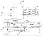
図11は、本発明を実施するための実施の形態3にかかる電力変換装置を適用した電力変換システムの構成図である。前記システム全体は、本実施の形態の電力変換装置100、直流電源1、電流センサ3とで構成されている。説明の便宜上、図11には負荷4も記載している。電力変換装置100は、直流電力を交流電力に変換するインバータの機能を有し、入力電源である直流電源1から供給される直流電力を交流電力に変換して負荷4に供給する。電流センサ3は電力変換装置100から負荷4に供給される電力に基づき検出電流信号Iuvwを出力する。なお、本実施の形態において電流センサ3は電力変換装置100と別に設ける構成としたが、電力変換装置100に含めて構成してもよい。
FIG. 11 is a configuration diagram of a power conversion system to which the power conversion device according to the third embodiment for carrying out the present invention is applied. The entire system is composed of the
また、実施の形態3においては、説明の便宜上、電力変換部2に接続されている負荷4は3相負荷とする。3相負荷の例としては、例えば永久磁石同期モータや誘導モータなどがあげられる。
Further, in the third embodiment, for convenience of explanation, the load 4 connected to the
図11に示すように、本実施の形態における電力変換装置100は、電力変換部2と制御部6とで構成されている。
As shown in FIG. 11, the
負荷4が3相負荷である場合、電力変換部2は例えば三相ブリッジ回路で構成される。三相ブリッジ回路の詳細は図11に記載していないが、u相、v相、w相の各相に対応する三相ブリッジ回路の回路は、実施の形態1および2の回路構成を示す図1と同様にIGBT201、211とFWD202、212によって構成される。P側スイッチング素子20およびN側スイッチング素子21が直列接続されている。さらに本実施の形態では、図1のスイッチング素子20および21を1セットとして、これらを並列に3つ接続し、計6個のスイッチング素子を用いたブリッジで構成されている。三相ブリッジ回路における上記各相のスイッチング素子20および21は、制御部6からのスイッチング指令Swuvw2*に基づいて駆動される。
When the load 4 is a three-phase load, the
電流センサ3は例えば、電力変換部2と負荷4とを接続する導線に設置されたシャント抵抗やカレントトランスなどである。電流センサ3は上記各相に設置されて、電力変換部2から負荷4に流れる三相電流を検出する。三相電流は、P側スイッチング素子20とN側スイッチング素子21との間からバスバー等を通じて負荷4の各相端子へそれぞれ流れて供給される。
The current sensor 3 is, for example, a shunt resistor or a current transformer installed in a lead wire connecting the
電流センサ3が上記各相に設けられている例を図11に図示して説明するが、電流センサ3は2個でもよい。この場合、既知の方法により検出した上記各相のうちの2相の電流値から3相の電流値を把握することが可能である。 An example in which the current sensors 3 are provided in each of the above phases will be illustrated and described with reference to FIG. 11, but the number of current sensors 3 may be two. In this case, it is possible to grasp the current value of the three phases from the current values of the two phases of the above-mentioned phases detected by a known method.
制御部6は、電流センサ3からの検出電流信号Iuvwに基づいて電力変換部2へスイッチング指令Swuvw2*を出力する。スイッチング指令Swuvw2*は、電力変換部2の上記各相のスイッチング素子20、21を駆動するための指令である。
The
制御部6のハード構成は実施の形態1および2と同様にプロセッサ601と記憶装置602とで構成されており、以下で説明する各部の機能を実現する。制御部6についてさらに説明する。
The hardware configuration of the
制御部6は、図11に示すように電圧指令生成部62、デッドタイム補償部(以下Td補償部と記載する)66、PWM処理部63、Td付加部64、シーケンス管理部61にて構成される。
As shown in FIG. 11, the
シーケンス管理部61は、実施の形態1および2の動作とは異なり、電流センサ3の検出電流信号Iuvwに基づいて、時間変化するデッドタイムの長さ指令Td*(t)をTd付加部64に出力する。また、係数αをTd補償部66に出力する。
Unlike the operations of the first and second embodiments, the
電圧指令生成部62は、電圧指令値Vuvw1*を生成し、Td補償部66へ出力する。このときの各相の電圧指令値Vuvw1*のそれぞれを(8)式に記載する。(8)式のVampは電圧指令振幅、θは電圧指令位相をそれぞれ示している。なお、本実施の形態における電圧指令値Vuvw1*の生成方法については特に問わずに適用できる。よって、(8)式に記載の3相の電圧指令値Vuvw1*は振幅と位相を記載した一般的な表現としている。
The voltage
Td補償部66はデッドタイム電圧誤差と逆極性の補償電圧を電圧指令値Vuvw1*に加算してデッドタイム補償を行う。Td補償部66は、検出電流信号Iuvwの極性とシーケンス管理部61からの係数αと、時間変化するデッドタイムの長さ指令Td*(t)とを受け取りデッドタイム補償を実施する。この結果、デッドタイム補償後の電圧指令値Vuvw2*は(9)式となる。(9)式のfcはキャリア周波数[Hz]、Vdcは電力変換部2への入力となる直流リンク電圧、sign(iu)、sign(iv)、sign(iw)は上記各相の出力電流の極性をそれぞれ示している。また、上記出力電流の極性は電力変換部2から負荷4に向かう方向dと一致する場合を正とし、正のとき1、負のとき−1とする。
The
PWM処理部63は、Td補償部66からのデッドタイム補償後の電圧指令値Vuvw2*を元にPWM処理を実施しスイッチング指令Swuvw1*をTd付加部64へ出力する。PWM処理は、三角波やノコギリ波との大小比較による処理を実施する。
The
Td付加部64は、PWM処理部63で処理されたスイッチング指令Swuvw1*にシーケンス管理部61からの時間変化するデッドタイムの長さ指令Td*(t)に従ってデッドタイムを付加する。そして、デッドタイムを付加したスイッチング指令Swuvw2*を電力変換部2へ出力する。
The
シーケンス管理部61についてさらに詳細に説明する。本実施の形態でシーケンス管理部61から出力される時間変化するデッドタイムの長さ指令Td*(t)は、(10)式となる。すなわちデッドタイムの長さ指令Td*(t)は所定の周波数で振動する。
The
(10)式中のTdAmpはTd長さの振動成分振幅、θtdは振動の位相を示している。振動の周波数は、他の外乱電圧の周波数成分を避けて設定される。また、デッドタイムの長さを振動させつつも、上記各相のスイッチング素子の上下短絡を防止するために、オフセット値Td_ofsを持たせている。(10)式は三角関数に基づいてデッドタイムの長さを振動させるものである。本実施の形態においては、デッドタイムの長さの振動が所定の周波数成分を持って振動すればよい。よって例えば矩形波形状に振動させてもよい。ここで周波数ftdとするとθtdとの関係は(11)式となる。 In equation (10), TdAmp indicates the amplitude of the vibration component of the Td length, and θtd indicates the phase of vibration. The frequency of vibration is set avoiding the frequency components of other disturbance voltages. Further, the offset value Td_ofs is provided in order to prevent the switching elements of the above phases from being vertically short-circuited while oscillating the length of the dead time. Equation (10) oscillates the length of the dead time based on the trigonometric function. In the present embodiment, the vibration having a dead time length may vibrate with a predetermined frequency component. Therefore, for example, it may be vibrated in a rectangular wave shape. Here, assuming that the frequency is ftd, the relationship with θtd is given by Eq. (11).
θtdの周波数を他の外乱電圧の周波数成分を避けて設定する理由について説明する。例えば負荷4として3相交流モータが接続されている場合、モータ自体が外乱電圧を出力することがある。永久磁石同期モータでは回転子の磁束と回転によって発生する誘起電圧高調波である。誘導モータでは相互インダクタンスの飽和による電圧歪みである。 The reason for setting the frequency of θtd while avoiding the frequency components of other disturbance voltages will be described. For example, when a three-phase AC motor is connected as the load 4, the motor itself may output a disturbance voltage. In a permanent magnet synchronous motor, it is an induced voltage harmonic generated by the magnetic flux and rotation of the rotor. In an induction motor, this is voltage distortion due to saturation of mutual inductance.
これらは3相静止座標上では複数の次数の高調波電圧成分を含み、負荷4であるモータの3相電流も同様の成分を含む。特に5次、7次の成分は顕著であり、これらは3相電流および3相電圧を2軸直交回転座標上に変換すると電力変換部2の交流出力電圧の周波数に対し6次の周波数成分を含むことが知られている。
These include harmonic voltage components of a plurality of orders on the three-phase rest coordinates, and the three-phase current of the motor, which is the load 4, also contains the same components. In particular, the 5th and 7th order components are remarkable, and when the three-phase current and the three-phase voltage are converted on the two-axis orthogonal rotation coordinates, the sixth-order frequency component with respect to the frequency of the AC output voltage of the
一方、デッドタイム電圧誤差も同様に3相静止座標上では矩形波に近い形状となり奇数次の高調波電圧成分を含む。同様に5次や7次の成分は顕著である。前記デッドタイム電圧誤差は2軸直交回転座標上においてはノコギリ状の電圧となり、6次の周波数成分となる。このデッドタイム電圧誤差に起因し2軸直交回転座標上の電流に6次の周波数成分が含まれることはよく知られた現象である。 On the other hand, the dead time voltage error also has a shape close to a square wave on the three-phase rest coordinates and includes odd-order harmonic voltage components. Similarly, the 5th and 7th order components are remarkable. The dead time voltage error becomes a saw-shaped voltage on the two-axis orthogonal rotating coordinates, and becomes a sixth-order frequency component. It is a well-known phenomenon that the current on the two-axis orthogonal rotating coordinates contains a sixth-order frequency component due to this dead time voltage error.
そのため、2軸直交回転座標上の電流の6次の周波数成分を利用したTd補償電圧の調整方式も提案されている。しかし、従来の方法では、モータ起因の6次の周期外乱電圧によって調整が阻害されデッドタイム補償精度が低下することがある。 Therefore, a method for adjusting the Td compensation voltage using the sixth-order frequency component of the current on the two-axis orthogonal rotating coordinates has also been proposed. However, in the conventional method, the adjustment may be hindered by the sixth-order periodic disturbance voltage caused by the motor, and the dead time compensation accuracy may decrease.
そこで本実施の形態では、デッドタイムの長さを時間変化させるにあたり、その周波数を外乱電圧の周波数成分とは異なる値に設定し、外乱電圧の影響を抑制する。具体的には、3相交流モータ負荷の場合、6次の周期以外の周期で時間変化させる。これにより係数αの誤差に起因する電流脈動成分の周波数と、モータ起因の外乱成分の周波数を異ならせることができる。その結果、モータ起因の外乱電圧の影響を受けることなく、係数αの調整ができる。また、調整された係数αを用いて補償することにより、デッドタイム補償精度を向上させることが可能となる。 Therefore, in the present embodiment, when the length of the dead time is changed with time, the frequency is set to a value different from the frequency component of the disturbance voltage to suppress the influence of the disturbance voltage. Specifically, in the case of a three-phase AC motor load, the time is changed in a cycle other than the sixth-order cycle. As a result, the frequency of the current pulsation component caused by the error of the coefficient α and the frequency of the disturbance component caused by the motor can be made different. As a result, the coefficient α can be adjusted without being affected by the disturbance voltage caused by the motor. Further, by compensating using the adjusted coefficient α, it is possible to improve the dead time compensation accuracy.
次に係数αの調整方法について説明する。
デッドタイムの長さ指令を時間変化させ、これに応じてデッドタイム補償を計算し実施する場合、係数αの正確な値が把握できていればよい。正確な値を把握することで、デッドタイム電圧誤差は抑制される。すなわち負荷4への出力電流には、該当の振動成分は含まれない。
Next, a method of adjusting the coefficient α will be described.
When the dead time length command is changed over time and the dead time compensation is calculated and implemented accordingly, it is sufficient if the accurate value of the coefficient α can be grasped. By grasping the accurate value, the dead time voltage error is suppressed. That is, the output current to the load 4 does not include the corresponding vibration component.
しかし、係数αの値の誤差が含まれると、負荷4への出力電流には上述の振動するデッドタイム電圧成分に起因する脈動が含まれる。このため、基本的には、デッドタイム電圧誤差の振動成分に起因する出力電流の脈動を検出する。そして、この脈動がゼロになるように調整すれば良い。そのため様々な方法を用いることができる。 However, if an error in the value of the coefficient α is included, the output current to the load 4 includes the pulsation caused by the above-mentioned oscillating dead time voltage component. Therefore, basically, the pulsation of the output current due to the vibration component of the dead time voltage error is detected. Then, the pulsation may be adjusted to be zero. Therefore, various methods can be used.
例えば係数αを所定の範囲で徐々に変化させる。その際の検出電流信号Iuvwに含まれるデッドタイム電圧誤差の振動に起因する周波数を持つ脈動成分の有無を記録する。そして、該電流脈動が最小となる係数αを調整結果として、最終的にTd補償部66へ出力する方式を用いる。この動作を適当な時間間隔で実施することで、負荷4への電力供給の間、高精度なデッドタイム補償が実現できる。
For example, the coefficient α is gradually changed within a predetermined range. At that time, the presence / absence of a pulsating component having a frequency due to the vibration of the dead time voltage error included in the detected current signal Iuvw is recorded. Then, a method is used in which the coefficient α that minimizes the current pulsation is finally output to the
他の方法として以下の方法を用いることができる。デッドタイム電圧誤差は、負荷4に3相正弦波交流電流が流れている状態を想定する。この場合、デッドタイム電圧誤差は、(2)式に従い矩形波に近い形状を持つ。電力変換部2の出力電圧の周波数をfとすると3相正弦波交流電流も同じ周波数fの電流となる。
The following method can be used as another method. The dead time voltage error assumes a state in which a three-phase sinusoidal alternating current is flowing through the load 4. In this case, the dead time voltage error has a shape close to a rectangular wave according to the equation (2). Assuming that the frequency of the output voltage of the
このとき(8)式に記載する電圧指令位相θの周波数もfとなる。デッドタイムの長さを時間変化させると(2)式に基づき矩形波となるデッドタイム電圧誤差の振幅を変動させることになる。一種の振幅変調となるため、デッドタイム電圧誤差中に含まれる振動成分はf+ftd、f−ftdの周波数成分を持つ。 At this time, the frequency of the voltage command phase θ described in the equation (8) is also f. When the length of the dead time is changed with time, the amplitude of the dead time voltage error which becomes a rectangular wave is changed based on the equation (2). Since it is a kind of amplitude modulation, the vibration component included in the dead time voltage error has frequency components of f + ftd and f−ftd.
また該矩形波形状のデッドタイム電圧誤差の基本波成分の位相は3相正弦波交流電流と同相となる。このため、デッドタイム電圧誤差の振動成分は相電流の振幅方向に主な成分を持つ。同様に該振動成分に起因する電流脈動も相電流の振幅方向に主な成分を持つ。 Further, the phase of the fundamental wave component of the dead time voltage error of the square wave shape is in phase with the three-phase sinusoidal alternating current. Therefore, the vibration component of the dead time voltage error has a main component in the amplitude direction of the phase current. Similarly, the current pulsation caused by the vibration component also has a main component in the amplitude direction of the phase current.
したがって、相電流信号にあたる検出電流信号Iuvwにおいて振幅を取り出せばデッドタイム電圧誤差の振動成分に起因する電流脈動を取り出すことができる。ただし3相であるため、全相をまとめて取り扱う必要がある。この場合、2軸直交回転座標上に変換した相電流ベクトルの大きさに該電流脈動が含まれる。 Therefore, if the amplitude is extracted in the detected current signal Iuvw corresponding to the phase current signal, the current pulsation caused by the vibration component of the dead time voltage error can be extracted. However, since there are three phases, it is necessary to handle all phases together. In this case, the current pulsation is included in the magnitude of the phase current vector converted on the two-axis orthogonal rotating coordinates.
これを(12)式と(13)式に示す。(12)式においては、座標変換位相は電圧指令位相θとしたが、電力変換部2の出力電圧あるいは3相交流電流と同じ周波数を持つ位相なら何でも良い。(13)式のinは検出電流ベクトルの振幅を示す。
This is shown in Eqs. (12) and (13). In the equation (12), the coordinate conversion phase is the voltage command phase θ, but any phase having the same frequency as the output voltage of the
(12)式において回転座標変換によって変換処理される信号の周波数成分のシフトが発生する。座標変換位相θの周波数はfである。(13)式に記載する相電流ベクトルの大きさinには、周波数シフトによって元のftdの周波数を持つ脈動が含まれる。 In equation (12), a shift of the frequency component of the signal converted by the rotating coordinate conversion occurs. The frequency of the coordinate transformation phase θ is f. The magnitude in of the phase current vector described in the equation (13) includes a pulsation having the original ftd frequency due to the frequency shift.
この電流脈動は上述のとおり、係数αの誤差に伴い発生する。よって相電流ベクトルの大きさinに基づき(14)式でαの調整を実施する。 As described above, this current pulsation occurs with an error of the coefficient α. Therefore, α is adjusted by Eq. (14) based on the magnitude in of the phase current vector.
(10)式においてデッドタイム電圧誤差の振動成分の位相θtdに対しcos成分で振動を発生させる。このとき、ftdを負荷4の電気時定数の逆数より十分大きな値に設定しておく。これにより、デッドタイム電圧誤差の振動成分は主に負荷4のインダクタンス成分が受け持つことになる。 In equation (10), vibration is generated by the cos component with respect to the phase θtd of the vibration component of the dead time voltage error. At this time, ftd is set to a value sufficiently larger than the reciprocal of the electric time constant of the load 4. As a result, the vibration component of the dead time voltage error is mainly handled by the inductance component of the load 4.
このためデッドタイム電圧誤差の振動成分に起因する電流脈動は、該電圧の振動成分に対し90度位相遅れの成分が主となる。(14)式はこれを反映し、位相θtdのsin信号で検波する簡易な構成となる。係数αの調整がなされると、(13)式に記載する相電流ベクトルの大きさinにはデッドタイム電圧誤差の振動成分に起因する電流脈動が含まれなくなる。したがって、(14)式の積分は自動的に停止する。(14)式中のKはα調整の応答速度を決めるゲインを示す。 Therefore, the current pulsation caused by the vibration component of the dead time voltage error is mainly composed of a component having a phase delay of 90 degrees with respect to the vibration component of the voltage. Eq. (14) reflects this and has a simple configuration for detecting with a sin signal having a phase θtd. When the coefficient α is adjusted, the magnitude in of the phase current vector described in Eq. (13) does not include the current pulsation caused by the vibration component of the dead time voltage error. Therefore, the integration of Eq. (14) is automatically stopped. K in Eq. (14) indicates the gain that determines the response speed of α adjustment.
このような方法を用いる場合、シーケンス管理部61は(10)式から(14)式を制御周期毎に実施しαの調整を実施する。この方法は常時動作が可能である。よって負荷4への電力供給中に係数αの変動が発生しても追従させることが可能となる。
When such a method is used, the
例えば、本方式に、キャリア周波数を振動させる従来の手法を適用させようとすると、キャリア周波数が局所的に低下する。その結果、電圧指令値がPWM電流リプルの影響を受け係数αの推定精度が低下する。また、変動するキャリア周波数にあわせ電流のサンプリングタイミングや電圧指令値の更新周期も変動するため、制御部6の構成が複雑となる問題が発生する。
For example, if a conventional method of vibrating the carrier frequency is applied to this method, the carrier frequency is locally lowered. As a result, the voltage command value is affected by the PWM current ripple, and the estimation accuracy of the coefficient α is lowered. Further, since the current sampling timing and the update cycle of the voltage command value also fluctuate according to the fluctuating carrier frequency, there arises a problem that the configuration of the
一方、本実施の形態においては、デッドタイムの長さを所定の周期で時間変化させデッドタイム電圧誤差を振動させる。このときデッドタイム補償も時間変化するデッドタイムの長さTd*(t)に応じ補償電圧を計算して実施する。よって、係数αの正確な値が把握できていれば、デッドタイム電圧誤差は抑制される。この結果、負荷4の電流には、該当の振動成分は含まれない。 On the other hand, in the present embodiment, the length of the dead time is changed with a predetermined cycle to vibrate the dead time voltage error. At this time, the dead time compensation is also performed by calculating the compensation voltage according to the length Td * (t) of the dead time that changes with time. Therefore, if the accurate value of the coefficient α can be grasped, the dead time voltage error can be suppressed. As a result, the current of the load 4 does not include the corresponding vibration component.
さらには、負荷4の電流に含まれる振動するデッドタイム電圧誤差成分に起因する電流脈動に対しては、電流脈動をゼロになるように係数αを調整する。これにより正確なαの値が取得できる。そして取得した係数αによって、デッドタイム電圧誤差以外の外乱電圧の影響を抑制することができる。 Further, for the current pulsation caused by the oscillating dead time voltage error component included in the current of the load 4, the coefficient α is adjusted so that the current pulsation becomes zero. As a result, an accurate value of α can be obtained. Then, the acquired coefficient α can suppress the influence of the disturbance voltage other than the dead time voltage error.
このように本実施の形態では、デッドタイム電圧誤差を外乱電圧の周波数成分とは異なる値で振動させることで外乱電圧の影響を抑制できる。また、デッドタイム電圧誤差成分に起因する電流脈動に対して、電流脈動をゼロになるように係数αを調整、取得することができる。よって電流リプルやノイズの影響を抑制して係数αを高精度に取得し、デッドタイム電圧誤差を補償する補償量を求めることができる。さらに、モータ起因の外乱電圧の影響を受けることなく係数αを調整できる効果に加え、負荷4に通常の電力供給を行いつつ、高精度なデッドタイム補償の実施も可能とする効果を奏する。 As described above, in the present embodiment, the influence of the disturbance voltage can be suppressed by vibrating the dead time voltage error with a value different from the frequency component of the disturbance voltage. Further, the coefficient α can be adjusted and acquired so that the current pulsation becomes zero with respect to the current pulsation caused by the dead time voltage error component. Therefore, it is possible to obtain the coefficient α with high accuracy by suppressing the influence of current ripple and noise, and to obtain the compensation amount to compensate for the dead time voltage error. Further, in addition to the effect that the coefficient α can be adjusted without being affected by the disturbance voltage caused by the motor, the effect is that it is possible to perform highly accurate dead time compensation while supplying normal power to the load 4.
実施の形態4.
実施の形態3ではデッドタイムの長さ指令を時間変化させ、デッドタイム電圧誤差を振動させて、出力電流に含まれるデッドタイム電圧誤差の振動に起因する電流脈動から係数αの調整を実施する構成を説明した。実施の形態4では、電圧指令値Vuvw*に基づいて係数αの調整を行う点が実施の形態3と相異している。その他構成については実施の形態3と同一または対応する構成を示しており、その説明を省略する。
Embodiment 4.
In the third embodiment, the dead time length command is changed with time, the dead time voltage error is vibrated, and the coefficient α is adjusted from the current pulsation caused by the vibration of the dead time voltage error included in the output current. Explained. The fourth embodiment is different from the third embodiment in that the coefficient α is adjusted based on the voltage command value Vuvw *. Other configurations are the same as or corresponding to those of the third embodiment, and the description thereof will be omitted.
図12に本実施の形態にかかる電力変換装置を適用した電力変換システムの構成図を示す。電圧指令生成部62には、電流センサ3からの電流検出信号Iuvwが入力される。電圧指令生成部62は、この電流検出信号Iuvwと例えば図示しない上位の制御出段からの電圧指令に応じて電流制御処理を行い、Td補償部66へ電圧指令値Vuvw*を出力する。また、シーケンス管理部61へも電圧指令値Vuvw*を出力する。
FIG. 12 shows a configuration diagram of a power conversion system to which the power conversion device according to the present embodiment is applied. The current detection signal Iuvw from the current sensor 3 is input to the voltage
シーケンス管理部61は、電流制御処理後の電圧指令Vuvw*が入力され、この電圧指令Vuvw*に基づいて係数αの調整が行われる。Td補償部66では、この電流制御処理後の電圧指令Vuvw*に逆極性の補償電圧を加算してデッドタイム補償を実施し、補償後の電圧指令値Vuvw2*を出力する。その他動作については、実施の形態3と同様であり、その説明を省略する。
The
デッドタイム電圧誤差起因の電流脈動は外乱であり、同様の周波数や振幅の信号が電流指令値に含まれる運転は一般的に非常に少ない。したがって制御部6の動作に電流制御処理が含まれる場合、電流脈動の成分を抑制するように電流制御処理が動作する。このため、電流制御処理の出力である電圧指令値Vuvw*には電流脈動と同じ周波数成分が逆極性で含まれる。よって電圧指令値Vuvw*に基づいて係数αの調整を行うことが可能である。
The current pulsation caused by the dead time voltage error is a disturbance, and the operation in which the signal of the same frequency and amplitude is included in the current command value is generally very small. Therefore, when the operation of the
このように、電圧指令値Vuvw*に基づいて係数αの調整が可能である実施の形態4は実施の形態1および2と同様に、係数αを高精度に取得し、デッドタイム電圧誤差を補償する補償量を求めることができる。また、実施の形態3と同様に、モータ起因の外乱電圧の影響を受けることなく係数αを調整でき、負荷4に通常の電力供給を行いつつ、高精度なデッドタイム補償の実施も可能とする効果を奏する。 As described above, in the fourth embodiment in which the coefficient α can be adjusted based on the voltage command value Vuvw *, the coefficient α is acquired with high accuracy and the dead time voltage error is compensated as in the first and second embodiments. The amount of compensation to be paid can be obtained. Further, as in the third embodiment, the coefficient α can be adjusted without being affected by the disturbance voltage caused by the motor, and it is possible to perform highly accurate dead time compensation while supplying normal power to the load 4. It works.
実施の形態5
実施の形態3および4では時間変化するデッドタイム長さを用いてデッドタイム電圧誤差を振動させ、出力電流または電圧指令に含まれるデッドタイム電圧誤差の振動に起因する電流脈動から係数αの調整を実施する構成を説明した。このとき時間変化するデッドタイムの長さの周波数は3相で同じ値とした。実施の形態5では、デッドタイムの長さを時間変化させる周波数が3相で異なるようにする構成が実施の形態3および4と相異している。その他構成については実施の形態3および4と同一または対応する構成を示しており、その説明を省略し、相違する部分について以下で説明する。
Embodiment 5
In the third and fourth embodiments, the dead time voltage error is oscillated using the time-varying dead time length, and the coefficient α is adjusted from the current pulsation caused by the vibration of the dead time voltage error included in the output current or the voltage command. The configuration to be implemented was explained. At this time, the frequency of the dead time that changes with time was set to the same value in the three phases. In the fifth embodiment, the configuration in which the frequency for changing the length of the dead time with time is different in the three phases is different from the third and fourth embodiments. Other configurations are the same as or corresponding to those of the third and fourth embodiments, the description thereof will be omitted, and the differences will be described below.
デッドタイムの長さを時間変化させる周波数が3相で異なる場合、実施の形態3および4におけるデッドタイム補償後の電圧指令値Vuvw2*を示す(9)式は(15)式となる。これにより、係数αの過剰または不足を相ごとに把握できる。これを利用すれば、3相個別に係数αの調整ができ、デッドタイム補償をより高精度化することができる。 When the frequency for changing the length of the dead time is different between the three phases, the equation (9) showing the voltage command value Vuvw2 * after the dead time compensation in the third and fourth embodiments becomes the equation (15). As a result, the excess or deficiency of the coefficient α can be grasped for each phase. By utilizing this, the coefficient α can be adjusted for each of the three phases, and the dead time compensation can be made more accurate.
Tdu*(t)はu相の時間に応じ変化するTd長さ、Tdv*(t)はv相の時間に応じ変化するTd長さ、Tdw*(t)はw相の時間に応じ変化するTd長さ、αuはu相の係数α、αvはv相の係数α、αwはw相の係数αをそれぞれ示している。 Tdu * (t) is the Td length that changes according to the time of the u phase, Tdv * (t) is the Td length that changes according to the time of the v phase, and Tdw * (t) changes according to the time of the w phase. The Td length and αu indicate the coefficient α of the u phase, αv indicates the coefficient α of the v phase, and αw indicates the coefficient α of the w phase.
デッドタイムの長さは(16)式、(17)式を用いて各相計算する。 The length of the dead time is calculated for each phase using the equations (16) and (17).
ftduはu相のTd長さの振動成分周波数、ftdvはv相のTd長さの振動成分周波数、ftdwはw相のTd長さの振動成分周波数をそれぞれ示している。 ftdu indicates the vibration component frequency of the Td length of the u phase, ftdv indicates the vibration component frequency of the Td length of the v phase, and ftdw indicates the vibration component frequency of the Td length of the w phase.
デッドタイム電圧誤差の振動に起因する電流脈動が相電流ベクトルの大きさに現れることは実施の形態3で説明した3相で同じデッドタイムの長さの時間変化させる場合と同じである。よって(12)式および(13)式は変更なく使用できる。3相の係数αの調整式は(14)式に変えて(18)式にて実施する。
The appearance of the current pulsation caused by the vibration of the dead time voltage error in the magnitude of the phase current vector is the same as the case where the three phases described in the third embodiment are changed by the same dead time length. Therefore, equations (12) and (13) can be used without change. The adjustment formula for the three-phase coefficient α is changed from the formula (14) to the formula (18).
例えば、本方式に、キャリア周波数を振動させる従来の手法を適用させるとする。この場合、キャリア周波数の変更によって3相個別でのαの調整には3相で個別の周波数を持つキャリアを用いる必要がある。このため3相の電圧で構成するPWM空間電圧ベクトルが大幅に崩れ電流が乱れる問題が発生する。 For example, it is assumed that the conventional method of vibrating the carrier frequency is applied to this method. In this case, it is necessary to use carriers having individual frequencies in the three phases to adjust α in the three phases individually by changing the carrier frequency. Therefore, there arises a problem that the PWM space voltage vector composed of the three-phase voltages is significantly collapsed and the current is disturbed.
一方、本実施の形態のようにデッドタイムの長さ自体を時間変化させる場合には、このような問題は発生しない。よって、3相で個別に係数αの調整が実施できる。 On the other hand, when the length of the dead time itself is changed with time as in the present embodiment, such a problem does not occur. Therefore, the coefficient α can be adjusted individually for the three phases.
このように本実施の形態は、実施の形態1から4と同様の効果に加え、3相で個別に係数αの調整することでより高精度なデッドタイム補償が可能となる効果を奏する。 As described above, in addition to the same effects as those in the first to fourth embodiments, the present embodiment has the effect of enabling more accurate dead time compensation by individually adjusting the coefficient α in the three phases.
なお、本発明は、発明の範囲内において、各実施の形態を自由に組み合わせることや、各実施の形態を適宜、変形、省略することが可能である。 In the present invention, each embodiment can be freely combined, and each embodiment can be appropriately modified or omitted within the scope of the invention.
1 直流電源、2 電力変換部、20 P側スイッチング素子、21 N側スイッチング素子、3 電流センサ、4 負荷、6 制御部、61 シーケンス管理部、62 電圧指令生成部、63 PWM処理部、64 デッドタイム付加部、65 電圧指令部、66 デッドタイム補償部、601 プロセッサ、602 記憶装置、201 P側IGBT、211 N側IGBT、202 P側FWD、212 N側FWD 1 DC power supply, 2 power conversion unit, 20 P side switching element, 21 N side switching element, 3 current sensor, 4 load, 6 control unit, 61 sequence management unit, 62 voltage command generator, 63 PWM processing unit, 64 dead Time addition unit, 65 voltage command unit, 66 dead time compensation unit, 601 processor, 602 storage device, 201 P side IGBT, 211 N side IGBT, 202 P side FWD, 212 N side FWD
Claims (7)
前記スイッチング素子をオフ状態とする保護期間であるデッドタイムの長さを決定するデッドタイムの長さ指令を出力するシーケンス管理部、および前記デッドタイムの長さ指令に基づいてデッドタイムを付加した前記スイッチング素子をオンおよびオフ動作させるスイッチング指令を出力するデッドタイム付加部、を有する制御部と、を備え、
前記シーケンス管理部は、前記デッドタイムの長さ指令に基づいた前記スイッチング指令によって前記スイッチング素子がオンおよびオフ動作されたときの前記電力変換部から前記負荷へ供給される電流値または前記スイッチング指令を生成するための電圧指令値に基づいて、前記電圧指令値を補償する補償量を求める電力変換装置。 A power converter that has a switching element and supplies current to the load,
A sequence management unit that outputs a dead time length command that determines the length of the dead time, which is a protection period for turning off the switching element, and the dead time added based on the dead time length command. A control unit having a dead time addition unit that outputs a switching command for operating the switching element on and off is provided.
The sequence management unit determines the current value supplied from the power conversion unit to the load or the switching command when the switching element is turned on and off by the switching command based on the dead time length command. A power conversion device that obtains a compensation amount for compensating for the voltage command value based on a voltage command value to be generated.
The control unit includes a dead time compensation unit that compensates by adding a compensation voltage having a polarity opposite to the voltage command value to the voltage command value based on the compensation amount, according to claims 1 to 6. The power conversion device according to any one item.
Priority Applications (1)
| Application Number | Priority Date | Filing Date | Title |
|---|---|---|---|
| JP2017079343A JP6787236B2 (en) | 2017-04-13 | 2017-04-13 | Power converter |
Applications Claiming Priority (1)
| Application Number | Priority Date | Filing Date | Title |
|---|---|---|---|
| JP2017079343A JP6787236B2 (en) | 2017-04-13 | 2017-04-13 | Power converter |
Publications (3)
| Publication Number | Publication Date |
|---|---|
| JP2018182901A JP2018182901A (en) | 2018-11-15 |
| JP2018182901A5 JP2018182901A5 (en) | 2020-01-16 |
| JP6787236B2 true JP6787236B2 (en) | 2020-11-18 |
Family
ID=64276234
Family Applications (1)
| Application Number | Title | Priority Date | Filing Date |
|---|---|---|---|
| JP2017079343A Active JP6787236B2 (en) | 2017-04-13 | 2017-04-13 | Power converter |
Country Status (1)
| Country | Link |
|---|---|
| JP (1) | JP6787236B2 (en) |
Families Citing this family (1)
| Publication number | Priority date | Publication date | Assignee | Title |
|---|---|---|---|---|
| JP7213196B2 (en) | 2020-02-28 | 2023-01-26 | 株式会社 日立パワーデバイス | MOTOR DRIVE DEVICE, OUTDOOR UNIT OF AIR CONDITIONER USING THE SAME, MOTOR DRIVE CONTROL METHOD |
-
2017
- 2017-04-13 JP JP2017079343A patent/JP6787236B2/en active Active
Also Published As
| Publication number | Publication date |
|---|---|
| JP2018182901A (en) | 2018-11-15 |
Similar Documents
| Publication | Publication Date | Title |
|---|---|---|
| JP6735827B2 (en) | Power converter | |
| US9755563B2 (en) | Inverter control apparatus and inverter apparatus | |
| JP6610804B2 (en) | Inverter control method, control device, and inverter | |
| CN108258975B (en) | Semiconductor device and power conversion device | |
| CN111149287A (en) | Power conversion device | |
| WO2015194493A1 (en) | Power conversion control device | |
| JP2015186432A (en) | Power conversion system, power conversion system control apparatus, and power conversion system control method | |
| CN103001568A (en) | Motor control device | |
| JP6787236B2 (en) | Power converter | |
| Kang et al. | Compensation for inverter nonlinearity considering voltage drops and switching delays of each leg's switches | |
| JP2005312274A (en) | Control device for ac motor | |
| Fischer et al. | Comparison of two power electronic topologies for power hardware in the loop machine emulator | |
| RU133990U1 (en) | DEVICE FOR CONTROLLING A TWO-PHASE ASYNCHRONOUS MOTOR IN A PULSE MOTION MODE | |
| Xie et al. | Improved INFORM method by minimizing the inverter nonlinear voltage error effects | |
| JP2016048997A (en) | Control method and device for power conversion system | |
| JP6753326B2 (en) | Motor control device | |
| JP2020031485A (en) | Power converter | |
| US11705841B2 (en) | Estimation device and AC motor drive device | |
| Fischer et al. | Current Control for a Multiphase Interleaved-Switched Inverter Using Field Oriented Coordinates | |
| CN114759812A (en) | Inverter operating at a high switching frequency and method for operating an inverter | |
| JP5910001B2 (en) | Power converter | |
| WO2017010142A1 (en) | Power conversion device | |
| KR101319303B1 (en) | Motor driving appararatus and method for controllling of the same | |
| US20210013811A1 (en) | Power conversion system and control method for voltage conversion circuit | |
| JP4857747B2 (en) | AC motor inverter device |
Legal Events
| Date | Code | Title | Description |
|---|---|---|---|
| A521 | Written amendment |
Free format text: JAPANESE INTERMEDIATE CODE: A523 Effective date: 20191127 |
|
| A621 | Written request for application examination |
Free format text: JAPANESE INTERMEDIATE CODE: A621 Effective date: 20191127 |
|
| A977 | Report on retrieval |
Free format text: JAPANESE INTERMEDIATE CODE: A971007 Effective date: 20200828 |
|
| TRDD | Decision of grant or rejection written | ||
| A01 | Written decision to grant a patent or to grant a registration (utility model) |
Free format text: JAPANESE INTERMEDIATE CODE: A01 Effective date: 20200929 |
|
| A61 | First payment of annual fees (during grant procedure) |
Free format text: JAPANESE INTERMEDIATE CODE: A61 Effective date: 20201012 |
|
| R151 | Written notification of patent or utility model registration |
Ref document number: 6787236 Country of ref document: JP Free format text: JAPANESE INTERMEDIATE CODE: R151 |