JP6774635B2 - Electronic device, light source device and projection device - Google Patents
Electronic device, light source device and projection device Download PDFInfo
- Publication number
- JP6774635B2 JP6774635B2 JP2017179290A JP2017179290A JP6774635B2 JP 6774635 B2 JP6774635 B2 JP 6774635B2 JP 2017179290 A JP2017179290 A JP 2017179290A JP 2017179290 A JP2017179290 A JP 2017179290A JP 6774635 B2 JP6774635 B2 JP 6774635B2
- Authority
- JP
- Japan
- Prior art keywords
- packing
- light source
- core member
- electronic device
- fixed
- Prior art date
- Legal status (The legal status is an assumption and is not a legal conclusion. Google has not performed a legal analysis and makes no representation as to the accuracy of the status listed.)
- Active
Links
Images


Classifications
-
- G—PHYSICS
- G03—PHOTOGRAPHY; CINEMATOGRAPHY; ANALOGOUS TECHNIQUES USING WAVES OTHER THAN OPTICAL WAVES; ELECTROGRAPHY; HOLOGRAPHY
- G03B—APPARATUS OR ARRANGEMENTS FOR TAKING PHOTOGRAPHS OR FOR PROJECTING OR VIEWING THEM; APPARATUS OR ARRANGEMENTS EMPLOYING ANALOGOUS TECHNIQUES USING WAVES OTHER THAN OPTICAL WAVES; ACCESSORIES THEREFOR
- G03B21/00—Projectors or projection-type viewers; Accessories therefor
- G03B21/14—Details
- G03B21/20—Lamp housings
- G03B21/2086—Security or safety means in lamp houses
-
- G—PHYSICS
- G03—PHOTOGRAPHY; CINEMATOGRAPHY; ANALOGOUS TECHNIQUES USING WAVES OTHER THAN OPTICAL WAVES; ELECTROGRAPHY; HOLOGRAPHY
- G03B—APPARATUS OR ARRANGEMENTS FOR TAKING PHOTOGRAPHS OR FOR PROJECTING OR VIEWING THEM; APPARATUS OR ARRANGEMENTS EMPLOYING ANALOGOUS TECHNIQUES USING WAVES OTHER THAN OPTICAL WAVES; ACCESSORIES THEREFOR
- G03B21/00—Projectors or projection-type viewers; Accessories therefor
- G03B21/14—Details
- G03B21/145—Housing details, e.g. position adjustments thereof
-
- G—PHYSICS
- G03—PHOTOGRAPHY; CINEMATOGRAPHY; ANALOGOUS TECHNIQUES USING WAVES OTHER THAN OPTICAL WAVES; ELECTROGRAPHY; HOLOGRAPHY
- G03B—APPARATUS OR ARRANGEMENTS FOR TAKING PHOTOGRAPHS OR FOR PROJECTING OR VIEWING THEM; APPARATUS OR ARRANGEMENTS EMPLOYING ANALOGOUS TECHNIQUES USING WAVES OTHER THAN OPTICAL WAVES; ACCESSORIES THEREFOR
- G03B21/00—Projectors or projection-type viewers; Accessories therefor
- G03B21/14—Details
- G03B21/16—Cooling; Preventing overheating
-
- G—PHYSICS
- G03—PHOTOGRAPHY; CINEMATOGRAPHY; ANALOGOUS TECHNIQUES USING WAVES OTHER THAN OPTICAL WAVES; ELECTROGRAPHY; HOLOGRAPHY
- G03B—APPARATUS OR ARRANGEMENTS FOR TAKING PHOTOGRAPHS OR FOR PROJECTING OR VIEWING THEM; APPARATUS OR ARRANGEMENTS EMPLOYING ANALOGOUS TECHNIQUES USING WAVES OTHER THAN OPTICAL WAVES; ACCESSORIES THEREFOR
- G03B21/00—Projectors or projection-type viewers; Accessories therefor
- G03B21/14—Details
- G03B21/20—Lamp housings
Landscapes
- Physics & Mathematics (AREA)
- General Physics & Mathematics (AREA)
- Engineering & Computer Science (AREA)
- Computer Security & Cryptography (AREA)
- Projection Apparatus (AREA)
- Casings For Electric Apparatus (AREA)
- Transforming Electric Information Into Light Information (AREA)
- Cooling Or The Like Of Electrical Apparatus (AREA)
- Arrangement Of Elements, Cooling, Sealing, Or The Like Of Lighting Devices (AREA)
- Non-Portable Lighting Devices Or Systems Thereof (AREA)
Description
本発明は、電子装置、光源装置及び投影装置に関する。 The present invention relates to an electronic device, a light source device and a projection device.
今日、パーソナルコンピュータの画面やビデオ画像、さらにメモリカード等に記憶されている画像データによる画像等をスクリーンに投影する画像投影装置として、データプロジェクタが多用されている。このプロジェクタは、光源から出射された光を、DMD(デジタル・マイクロミラー・デバイス)と呼ばれるマイクロミラー表示素子、又は、液晶板に集光させ、スクリーン上にカラー画像を表示させるものである。 Today, a data projector is widely used as an image projection device for projecting a screen of a personal computer, a video image, an image based on image data stored in a memory card or the like, or the like on the screen. This projector collects the light emitted from the light source on a micromirror display element called a DMD (Digital Micromirror Device) or a liquid crystal plate, and displays a color image on the screen.
プロジェクタは、パーソナルコンピュータやDVDプレーヤーなどの映像機器の普及に伴って、業務用プレゼンテーションから家庭用に至るまで、用途が拡大している。このようなプロジェクタにおいて、従来は高輝度の放電ランプを光源とするものが主流であったが、近年、レーザダイオード等の固体発光素子や、この固体発光素子を励起光源とする蛍光板を光源として備える投影装置が種々開発されている。 With the widespread use of video equipment such as personal computers and DVD players, projectors are expanding their applications from business presentations to home use. Conventionally, such projectors use a high-intensity discharge lamp as a light source, but in recent years, a solid-state light emitting element such as a laser diode or a fluorescent plate using this solid-state light emitting element as an excitation light source is provided as a light source. Various projection devices have been developed.
このような投影装置は、光源装置を構成するケースの内部に、光を出射するレーザダイオード等を外部から取り付ける構成を採ることがある。例えば、特許文献1には、放熱装置と、複数の半導体発光素子である青色レーザダイオードを保持するホルダとを備えた光源装置が開示されている。放熱装置は、青色レーザダイオードが配置される側とは反対側の面と接するように配置される。 Such a projection device may have a configuration in which a laser diode or the like that emits light is attached from the outside inside a case that constitutes the light source device. For example, Patent Document 1 discloses a light source device including a heat radiating device and a holder for holding a blue laser diode which is a plurality of semiconductor light emitting elements. The heat radiating device is arranged so as to be in contact with the surface opposite to the side on which the blue laser diode is arranged.
近年投影装置の使用環境は防塵性が求められており、その為には光源装置に密閉構造を施すことが望ましい。特にレーザダイオードやLEDは、光路に侵入した粉塵等の影響を受けて輝度低下等の現象を起こすことがあるため、これを防止するために光源装置の隙間を密閉する技術が必要である。 In recent years, the usage environment of the projection device has been required to be dustproof, and for that purpose, it is desirable to provide a sealed structure to the light source device. In particular, laser diodes and LEDs may cause a phenomenon such as a decrease in brightness due to the influence of dust or the like that has entered the optical path, and in order to prevent this, a technique for sealing the gap of the light source device is required.
しかしながら、上述の特許文献1の光源装置は、ホルダに対して、放熱装置が配置される側から、青色レーザダイオードが配置される側への封止構造が特段設けられていない。そのため、光学部材が配置されるケースの内部に、外部から粉塵などの異物が流入することが想定される。光学部材への異物の付着等は、光源装置内における導光を妨げ、その結果、光源装置が出射する光の品質を低下させる。 However, the light source device of Patent Document 1 described above is not particularly provided with a sealing structure for the holder from the side where the heat dissipation device is arranged to the side where the blue laser diode is arranged. Therefore, it is assumed that foreign matter such as dust flows into the case where the optical member is arranged from the outside. Adhesion of foreign matter to the optical member hinders light guidance in the light source device, and as a result, deteriorates the quality of the light emitted by the light source device.
一方、光学部材は設計された位置からずれると光学特性を悪化させる。そのため、ケースと固定対象部材との間等に、防塵のための封止部材を配置させるときに、光学部材の位置ずれも防ぐ必要がある。 On the other hand, if the optical member deviates from the designed position, the optical characteristics deteriorate. Therefore, it is necessary to prevent the positional deviation of the optical member when the sealing member for dust prevention is arranged between the case and the member to be fixed.
本発明は、以上の点に鑑み、固定対象部材の位置ずれを低減しながら防塵性を向上させた電子装置、光源装置及び投影装置を提供することを目的とする。 In view of the above points, it is an object of the present invention to provide an electronic device, a light source device, and a projection device having improved dust resistance while reducing misalignment of the member to be fixed.
本発明に係る電子装置は、固定対象部材と、前記固定対象部材の周囲に立設する枠部が形成された被固定部と、環状に形成された溝を有し、前記枠部と前記固定対象部材との間に環状に形成されたパッキンと、前記溝に配置される芯部材と、前記芯部材を前記パッキンの方向へ押圧する押圧部材と、前記固定対象部材に取り付けられ、突出部を有する基板と、を備え、前記芯部材は、一端側と他端側に切断部を有し、前記芯部材の前記切断部は、前記芯部材の対向する部位の一方の中央付近に配置され、前記押圧部材が押圧する前記芯部材の対向する部位は、前記基板の前記突出部と対応する部位を除いた領域である。
また、本発明に係る他の電子装置は、固定対象部材と、前記固定対象部材の周囲に立設する枠部が形成された被固定部と、溝を有し、前記枠部と前記固定対象部材との間に配置されるパッキンと、前記溝に配置される芯部材と、前記芯部材を前記パッキンの方向へ押圧する押圧部材と、を備え、前記固定対象部材は前記被固定部に直接固定されている。
本発明に係る更に他の電子装置は、固定対象部材と、前記固定対象部材の周囲に立設する枠部が形成された被固定部と、溝を有し、前記枠部と前記固定対象部材との間に配置されるパッキンと、前記溝に配置される芯部材と、前記芯部材を前記パッキンの方向へ押圧する押圧部材と、を備え、前記パッキンの内周面と前記固定対象部材の外側面との間隙は封止され、前記パッキンの外周面と前記枠部の内周面との間隙も封止される。
The electronic device according to the present invention has a fixing target member, a fixed portion in which a frame portion to be erected around the fixing target member is formed, and a groove formed in an annular shape, and the frame portion and the fixing are provided. A packing formed in an annular shape between the target member, a core member arranged in the groove, a pressing member for pressing the core member in the direction of the packing, and a protruding portion attached to the fixing target member. comprising a substrate having, a, the core member has a cutting portion at one end and the other end, the cutting portion of the core member is disposed on one near the center of the site which pairs direction of the core member , sites where the pressing member against direction of the core member for pressing is a region excluding the region corresponding to the protruding portion of the substrate.
Further, another electronic device according to the present invention has a fixing target member, a fixed portion in which a frame portion to be erected around the fixing target member is formed, and a groove, and the frame portion and the fixing target are provided. A packing arranged between the members, a core member arranged in the groove, and a pressing member for pressing the core member in the direction of the packing are provided, and the fixing target member is directly attached to the fixed portion. It is fixed.
Yet another electronic device according to the present invention has a fixing target member, a fixed portion in which a frame portion to be erected around the fixing target member is formed, and a groove, and the frame portion and the fixing target member. A packing arranged between the two, a core member arranged in the groove, and a pressing member for pressing the core member in the direction of the packing, and the inner peripheral surface of the packing and the fixing target member The gap with the outer side surface is sealed, and the gap between the outer peripheral surface of the packing and the inner peripheral surface of the frame portion is also sealed.
本発明に係る光源装置は、上記の電子装置を備え、前記被固定部は、前記固定位置に開口部が形成された光源ケースであり、前記固定対象部材は、光源を保持するホルダであり、前記押圧部材は、前記芯部材を押圧しながら前記ホルダと当接する、前記ホルダのヒートシンクである。 The light source device according to the present invention includes the above-mentioned electronic device, the fixed portion is a light source case having an opening formed at the fixed position, and the fixing target member is a holder for holding the light source. The pressing member is a heat sink of the holder that comes into contact with the holder while pressing the core member.
本発明に係る投影装置は、上記の光源装置と、前記光源装置からの光源光が照射され、画像光を形成する表示素子と、前記表示素子から出射された前記画像光をスクリーンに投影する投影側光学系と、前記表示素子と前記光源装置を制御する投影装置制御部と、を有する。 The projection device according to the present invention includes the above-mentioned light source device, a display element that is irradiated with the light source light from the light source device to form an image light, and a projection that projects the image light emitted from the display element onto a screen. It has a side optical system, a projection device control unit that controls the display element and the light source device.
本発明によれば、固定対象部材の位置ずれを低減しながら防塵性を向上させた電子装置、光源装置、投影装置を提供することができる。 According to the present invention, it is possible to provide an electronic device, a light source device, and a projection device having improved dust resistance while reducing the positional deviation of the member to be fixed.
(実施形態1)
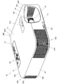
以下、本発明を実施するための形態について説明する。図1は、投影装置10の外観斜視図である。本実施形態の投影装置10は、上本体ケース10a及び下本体ケース10bを備える。投影装置10の筐体の側板である正面パネル12、背面パネル13、右側パネル14、及び左側パネル15は、上本体ケース10aの外周縁から下方に向かって立設する。各パネル12〜15の下端は、下本体ケース10bの外周縁と当接する。したがって、投影装置10は、上本体ケース10aと下本体ケース10bにより略直方体状に形成される。なお、本実施形態において、投影装置10における左右とは投影方向に対しての左右方向を示し、前後とは投影装置10のスクリーン側方向及び光線束の進行方向に対しての前後方向を示す。
(Embodiment 1)
Hereinafter, modes for carrying out the present invention will be described. FIG. 1 is an external perspective view of the
投影装置10の筺体の上面パネル11には、キー/インジケータ部37、投影画像調整部11aが設けられる。このキー/インジケータ部37には、電源スイッチキーや電源のオン又はオフを報知するパワーインジケータ、投影のオン、オフを切りかえる投影スイッチキー、光源装置や表示素子又は制御回路等が過熱した時に報知をする過熱インジケータ等の各種設定を行うためのキーやインジケータが配置されている。投影画像調整部11aは、一つ又は複数の回動摘みを備える。この回動摘みを操作することにより、図4で後述する投影側光学系の可動レンズの位置が調節され、投影画像の大きさやピントの調整が行われる。また、投影装置10は、図示しないが、リモートコントローラからの制御信号を受信するIr受信部を備えている。
A key /
正面パネル12と右側パネル14の前方右側の角部501には、吸気孔310が設けられる。正面パネル12の左側には、すり鉢状に窪んだ光出射部12aが設けられる。この光出射部12aの左側パネル15側の内壁には、吸気孔320が形成される。投影装置10は、光出射部12aに、投影口12bと、投影口12bを覆うレンズカバー19を有する。
正面パネル12の下端には、高さ調整ボタン12cが設けられる。投影装置10は、正面パネル12側の内部に支脚を備える。投影装置10は、高さ調整ボタン12cが押下されている間、下方からその支脚を出没させることができる。よって、使用者は、高さ調整ボタン12cを操作することにより支脚を任意の出代量で固定し、投影装置10の高さや傾きを調節することができる。
A
背面パネル13には、USB端子や画像信号入力用のD−SUB端子、S端子、RCA端子等を設ける入出力コネクタ部及び電源アダプタプラグ等の各種端子20が設けられている。また、背面パネル13において、右側パネル14側の角部503に吸気孔330が形成され、左側パネル15側の角部504にも排気孔340が形成される。
The
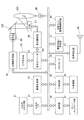
つぎに、投影装置10の投影装置制御部について図2の機能ブロック図を用いて説明する。投影装置制御部は、制御部38、入出力インターフェース22、画像変換部23、表示エンコーダ24、表示駆動部26等から構成される。
Next, the projection device control unit of the
制御部38は、投影装置10内の各回路の動作制御を司るものであって、CPUや各種セッティング等の動作プログラムを固定的に記憶したROM及びワークメモリとして使用されるRAM等により構成されている。
The
そして、この投影装置制御部により、入出力コネクタ部21から入力された各種規格の画像信号は、入出力インターフェース22、システムバス(SB)を介して画像変換部23で表示に適した所定のフォーマットの画像信号に統一するように変換された後、表示エンコーダ24に出力される。
Then, the image signals of various standards input from the input /
表示エンコーダ24は、入力された画像信号をビデオRAM25に展開記憶させた上でこのビデオRAM25の記憶内容からビデオ信号を生成して表示駆動部26に出力する。
The
表示駆動部26は、表示エンコーダ24から出力された画像信号に対応して適宜フレームレートで空間的光変調素子(SOM)である表示素子51を駆動するものである。
The
投影装置10は、光源装置60から出射された光源光の光線束を、後述する導光光学系を介して表示素子51に照射することにより、表示素子51の反射光で光像(画像)を形成する。投影装置10は、その形成した光像を同じく後述する投影側光学系を介してスクリーンに投影し、画像を表示させる。なお、この投影側光学系の可動レンズ群235は、レンズモータ45によりズーム調整やフォーカス調整のための駆動が行われる。
The
画像圧縮/伸長部31は、画像信号の輝度信号及び色差信号をADCT及びハフマン符号化等の処理によりデータ圧縮して着脱自在な記録媒体とされるメモリカード32に順次書き込む記録処理を行う。
The image compression /
また、画像圧縮/伸長部31は、再生モード時はメモリカード32に記録された画像データを読み出し、一連の動画を構成する個々の画像データを1フレーム単位で伸長する。そして、画像圧縮/伸長部31は、その画像データを、画像変換部23を介して表示エンコーダ24に出力し、メモリカード32に記憶された画像データに基づいた動画等を表示する処理を行う。
Further, the image compression /
筺体の上面パネル11に設けられるメインキー及びインジケータ等により構成されるキー/インジケータ部37の操作信号は、直接に制御部38に送出される。リモートコントローラからのキー操作信号は、Ir受信部35で受信され、Ir処理部36で復調されたコード信号が制御部38に出力される。
The operation signal of the key /
なお、制御部38にはシステムバス(SB)を介して音声処理部47が接続されている。この音声処理部47は、PCM音源等の音源回路を備えており、投影モード及び再生モード時には音データをアナログ化し、スピーカ48を駆動して拡声放音させる。
A
また、制御部38は、光源制御手段としての光源制御回路41を制御している。この光源制御回路41は、画像生成時に要求される所定波長帯域の光が光源装置60から出射されるように、光源装置60の緑色光源装置における励起光照射装置や、赤色光源装置の発光を個別に制御する。光源装置60から出射された所定の波長帯域の光は、照射ミラー185で反射され、表示素子51に照射される。
Further, the
制御部38は、冷却ファン駆動制御回路43に光源装置60等に設けた複数の温度センサによる温度検出を行わせ、この温度検出の結果から冷却ファンの回転速度を制御させている。また、制御部38は、投影装置10の電源をOFFにする指示を受けると、冷却ファン駆動制御回路43にタイマーを用いて投影装置10本体の電源OFF後も冷却ファンの回転を持続させたり、温度センサによる温度検出の結果に応じて投影装置10本体の電源を切るタイミングを定める等の制御を行うことができる。
The
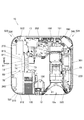
つぎに、投影装置10の内部構造について述べる。図3は、投影装置10の内部構造を示す平面模式図である。投影装置10は、電源装置301、制御回路基板302、光源装置60を備える。また、投影装置10は、冷却ファンとして、吸気ファン260、吸気ファン270、排気ファン280を備える。
Next, the internal structure of the
光源装置60は、投影装置10の筐体の略中央に配置される。光源装置60は、光源ケース61によって、内部に光源、レンズ、ミラー等の光学部材を収容する。電源装置301は、光源装置60の左側パネル15側に配置される。電源装置301の基板は、左側パネル15と略平行に配置される。制御回路基板302は、光源装置60の背面パネル13側に配置される。制御回路基板302は、上下方向に対し略垂直に配置される。制御回路基板302は、電源回路ブロックや光源制御ブロック等を備える。また、制御回路基板302は、電源回路ブロックや光源制御ブロック等の機能毎に分けて、複数備えることができる。
The
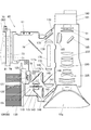
ここで、光源装置60の内部構造について説明する。図4は、光源装置60の平面模式図である。光源装置60は、赤色波長帯域光の光源である赤色光源装置120と、緑色波長帯域光の光源である緑色光源装置80と、青色波長帯域光の光源である青色光源装置であると共に励起光源でもある励起光照射装置70と、を備える。緑色光源装置80は、励起光照射装置70と、蛍光板装置100により構成される。光源装置60は、導光光学系140を有する。導光光学系140は、緑色波長帯域光及び青色波長帯域光及び赤色波長帯域光の光線束を合わせて、各色波長帯域の光線束を同一光路上に導光する。
Here, the internal structure of the
励起光照射装置70は、投影装置10筐体の右側パネル14側に配置される。励起光照射装置70は、背面パネル13と光軸が平行になるよう配置された複数の固体発光素子を備える。本実施形態の固体発光素子は、青色波長帯域光を発する複数の青色レーザダイオード71である。また、複数の青色レーザダイオード71は、右側パネル14と平行に並べて配置されている。これら青色レーザダイオード71は、ホルダ(固定対象部材)74に固定される。
The excitation
また、励起光照射装置70は、反射ミラー76、拡散板78、ヒートシンク(押圧部材)81を備える。反射ミラー76は、各青色レーザダイオード71からの出射光の光軸を拡散板78に向けて略90度変換する。拡散板78は、反射ミラー76で反射した各青色レーザダイオード71からの出射光を予め定められた拡散角度で拡散する。図3に示すように、ヒートシンク81は、青色レーザダイオード71と右側パネル14との間に配置される。
Further, the excitation
図4に戻り、各青色レーザダイオード71からの光路上には、青色レーザダイオード71からの出射光の指向性を高めて平行光に変換するコリメータレンズ73が夫々配置されている。これらコリメータレンズ73は、青色レーザダイオード71とともにホルダ74に保持される。
Returning to FIG. 4,
赤色光源装置120は、青色レーザダイオード71の光線束と光軸が平行となるように配置された赤色光源121と、赤色光源121からの出射光を集光する集光レンズ群125と、を備える。この赤色光源121は、赤色波長帯域光を出射する固体発光素子である赤色発光ダイオードである。赤色光源装置120は、赤色光源装置120が出射する赤色波長帯域光の光軸が、蛍光板101から出射される緑色波長帯域光の光軸と交差するように配置される。また、赤色光源装置120は、赤色光源121の右側パネル14側にヒートシンク130を備える。
The red
緑色光源装置80を構成する蛍光板装置100は、蛍光板101、モータ110、入射側の集光レンズ117a,117b、出射側の集光レンズ115を備える。蛍光板101は、励起光照射装置70からの出射光の光軸と直交するように配置された蛍光ホイールである。この蛍光板101はモータ110により回転駆動する。集光レンズ117a,117bは、励起光照射装置70から出射される励起光の光線束を蛍光板101に集光する。集光レンズ115は、蛍光板101から正面パネル12方向に出射される光線束を集光する。なお、蛍光板装置100は、集光レンズ117a,117b,115の上方に配置される。そのため、蛍光板101の下方の一部が集光レンズ117a,117b,115の光路上に配置される。
The
蛍光板101には、蛍光発光領域と拡散透過領域とが周方向に並設されている。蛍光発光領域は、青色レーザダイオード71から出射された青色波長帯域光を励起光として受けて、励起された緑色波長帯域の蛍光光を出射する。拡散透過領域は、青色レーザダイオード71からの出射光を拡散透過する。拡散透過した出射光は、光源装置60の青色波長帯域光として出射される。
On the
導光光学系140は、第一ダイクロイックミラー141、集光レンズ149、第二ダイクロイックミラー148、第一反射ミラー143、集光レンズ146、第二反射ミラー145、集光レンズ147を有する。第一ダイクロイックミラー141は、励起光照射装置70から出射される青色波長帯域光及び蛍光板101から出射される緑色波長帯域光と、赤色光源装置120から出射される赤色波長帯域光とが交差する位置に配置される。第一ダイクロイックミラー141は、青色波長帯域光及び赤色波長帯域光を透過し、緑色波長帯域光を反射する。第一ダイクロイックミラー141が反射した緑色波長帯域光の光軸は、集光レンズ149に向かう左側パネル15方向に90度変換される。したがって、第一ダイクロイックミラー141を透過した赤色波長帯域光の光軸は、第一ダイクロイックミラー141により反射された緑色波長帯域光の光軸と一致する。
The light guide
集光レンズ149は、第一ダイクロイックミラー141の左側パネル15側に配置される。第一ダイクロイックミラー141を透過した赤色波長帯域光及び第一ダイクロイックミラー141により反射された緑色波長帯域光は、共に集光レンズ149に入射する。第二ダイクロイックミラー148は、集光レンズ149の左側パネル15側であって、集光レンズ147の背面パネル13側に配置される。第二ダイクロイックミラー148は、赤色波長帯域光及び緑色波長帯域光を反射し、青色波長帯域光を透過する。したがって、集光レンズ149で集光された赤色波長帯域光及び緑色波長帯域光は、第二ダイクロイックミラー148によって反射されて、背面パネル13側に90度変換される。第二ダイクロイックミラー148の背面パネル13側には、集光レンズ173が配置される。第二ダイクロイックミラー148により反射された赤色波長帯域光及び緑色波長帯域光は、集光レンズ173に入射する。
The
第一反射ミラー143は、蛍光板101を透過した青色波長帯域光の光軸上、つまり、集光レンズ115と正面パネル12との間に配置される。第一反射ミラー143は、青色波長帯域光を反射して、この青色波長帯域光の光軸を左側パネル15方向に90度変換する。集光レンズ146は、第一反射ミラー143の左側パネル15側に配置される。また、第二反射ミラー145は、集光レンズ146の左側パネル15側に配置される。第二反射ミラー145は、第一反射ミラー143により反射されて、集光レンズ146により集光された青色波長帯域光の光軸を、背面パネル13側に90度変換する。集光レンズ147は、第二反射ミラー145の背面パネル13側に配置される。第二反射ミラー145により反射された青色波長帯域光は、集光レンズ147を介して第二ダイクロイックミラー148を透過し、集光レンズ173に入射する。このようにして、導光光学系140により導光された赤色、緑色、青色の各波長帯域光の光線束は、光源側光学系170の同一光路上に導光される。
The
光源側光学系170は、集光レンズ173、ライトトンネルやガラスロッド等の導光装置175、集光レンズ178、光軸変換ミラー179、集光レンズ183、照射ミラー185、コンデンサレンズ195を備える。なお、コンデンサレンズ195は、コンデンサレンズ195の背面パネル13側に配置される表示素子51から出射された画像光を、投影側光学系220に向けて出射するため、投影側光学系220の一部でもある。
The light source side
集光レンズ173から出射した各光線束は、導光装置175に入射する。導光装置175に入射される各光線束は、導光装置175により均一な強度分布の光線束となる。
Each light beam bundle emitted from the
導光装置175の背面パネル13側の光軸上には、集光レンズ178を介して、光軸変換ミラー179が配置されている。導光装置175の出射口から出射した光線束は、集光レンズ178で集光された後、光軸変換ミラー179により、集光レンズ183に向かう光軸に変換される。
An optical
光軸変換ミラー179で反射した光線束は、集光レンズ183により集光された後、照射ミラー185により、コンデンサレンズ195を介して表示素子51に所定の角度で照射される。なお、表示素子51の背面パネル13側にはヒートシンク190が設けられている。DMDとされる表示素子51は、このヒートシンク190により冷却される。また、ヒートシンク190の後方に形成されたフィン191の板面は、上下方向に対して垂直に形成される。
The light beam reflected by the optical
光源側光学系170により表示素子51の画像形成面に照射された光源光である光線束は、表示素子51の画像形成面で反射され、投影光として投影側光学系220を介してスクリーンに投影される。
The light bundle, which is the light source light emitted from the image forming surface of the
投影側光学系220は、コンデンサレンズ195、可動レンズ群235、固定レンズ群225により構成される。固定レンズ群225は、固定鏡筒に内蔵される。可動レンズ群235は、可動鏡筒に内蔵され、手動又は自動により移動されることにより、ズーム調整やフォーカス調整を可能としている。
The projection side
このように投影装置10を構成することで、蛍光板101を回転させるとともに励起光照射装置70及び赤色光源装置120から異なるタイミングで光を出射すると、赤色、緑色及び青色の各波長帯域光が導光光学系140を介して導光装置175に入射され、さらに光源側光学系170を介して表示素子51に入射される。よって、投影装置10の表示素子51であるDMDがデータに応じて各色の光を時分割表示することにより、スクリーンにカラー画像を投影することができる。
By configuring the
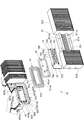
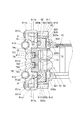
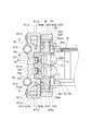
つぎに、励起光照射装置70の構成について説明する。図5は、励起光照射装置70のヒートシンク81、固定対象部材であるホルダ74、パッキン91、芯部材92を含む分解斜視図である。図6は、図3の励起光照射装置70周辺のVI−VI断面図である。図7は、図6の励起光照射装置70周辺のVII−VII断面図である。なお、以下の励起光照射装置70の説明において、光源ケース61側を前、ヒートシンク81側を後として説明する。
Next, the configuration of the excitation
ヒートシンク81は、ベース部材811と、複数のフィンで形成されるフィンユニット812と、を有する。ベース部材811は略矩形の板状に形成される。ベース部材811は、図6に示すように、上端部及び下端部から光源ケース61側へ立設する押えブロック811a,811bを有する。ベース部材811は、上端側及び下端側に、それぞれ2個の螺子用の貫通孔811dを有する。押えブロック811a,811bは、左右方向に貫通する中空構造を有している。また、各押えブロック811a,811bの被固定部62側の当接面811cは、平坦面として形成される。
The
図5において、ベース部材811と、フィンユニット812の各フィンとは、2本のヒートパイプ813によって接続される。ベース部材811とヒートパイプ813とは、ろう付け等により互いに固着され、両者は熱伝導性を有する。また、各フィンユニット812は、ベース部材811の両側に配置される。
In FIG. 5, the
ホルダ74は、略直方体状に形成される。ホルダ74は、ヒートシンク81側に、長手方向に形成された溝741を有する。この溝741の略中央には、同じく長手方向に延設される2個の中間壁742,743が形成される。中間壁742及び中間壁743は、長手方向に並設される。中間壁742,743を含むホルダ74の溝741側の表面74aは、略同一平面上に形成される(図6及び図7参照)。
The
ホルダ74の溝741には、基板75が配置される。基板75は、ホルダ74の長手方向と同方向に長軸を有した略長矩形状に形成される。基板75は、青色レーザダイオード71へ電力を供給する配線部751と、電源や制御回路等と接続される接続部(突出部)752と、を有する。配線部751は、接続部752よりも狭い幅で形成される。配線部751には、基板75の長手方向に形成される2個の貫通孔753,754が形成される。貫通孔753内には中間壁742が挿入され、貫通孔754内には中間壁743が挿入されて、配線部751が溝741内に配置される。ホルダ74の4隅には、ヒートシンク81側から光源ケース61側へ向かう前後方向に貫通する螺子用孔744が形成される。
The
なお、ホルダ74の側面74c,74dは、図7に示すように、ヒートシンク81側の幅が被固定部62側の幅よりも狭いテーパ状に形成される。
As shown in FIG. 7, the side surfaces 74c and 74d of the
パッキン91は、シリコンゴム等の軟質の弾性部材により、略長矩形の環状に形成される。パッキン91のヒートシンク81が配置される側は、略平坦面91aとして形成される。平坦面91aには、溝911が形成される。溝911は、パッキン91の外縁91a1と内縁91a2との間の略中央に環状に配置される。また、溝911の断面形状は、略凹円弧形状である。パッキン91の内側に形成される開口部912は、各内角部が略直角な長矩形状に形成される。パッキン91の外縁91a1の角部は、円弧状に形成される。
The packing 91 is formed of a substantially long rectangular ring by a soft elastic member such as silicon rubber. The side of the packing 91 on which the
芯部材92は、その断面がパッキン91の溝911の内径と略同じ外径で全体が略長矩形の環状に形成される。芯部材92の断面は略円形状に形成される。芯部材92には、金属等(例えばステンレス)の硬質の部材が使用される。具体的には、芯部材92は、棒状の部材を折り曲げて略環状になるように形成する。従って、環状に形成しても芯部材92の一端側と他端側に切断部が存在する。
The
光源ケース61は、フランジ状に拡幅した被固定部62を備える。被固定部62は、ホルダ74及びヒートシンク81の、光源ケース61に対する固定位置である。被固定部62の中央側には、略長矩形状の開口部621が形成される。この開口部621により、光源ケース61の内外の空間が接続される。光源ケース61の開口部621の周辺には、平面部622が形成される。平面部622には、開口部621の縁部周辺において略長矩形状に窪んだ段部623が形成される。
The
開口部621の上方の長辺側の段部623には、位置決め突起623aが形成される(図6参照)。また、開口部621の長辺側の両段部623には、各々3個の螺子孔623bが形成される。
A
開口部621の短辺側には、段部623の底面より高く、平面部622よりも低い略矩形状の段部624が形成される。各段部624には、突起である位置決め係合部624aと、2個の螺子孔624bとが形成される。
On the short side side of the
被固定部62には、平面部622から立設する略長矩形状の枠部625が形成される。枠部625は、開口部621を囲うように、開口部621の外周側の周囲に設けられる。枠部625の各角部625aは、略円弧状に形成される。枠部625の長辺である上辺及び下辺には、各々2個の円弧状の膨出部625cが形成される。各膨出部625cには、螺子孔625bが形成される。
The fixed
枠部625内における、平面部622上には、薄板状の緩衝部材626が配置される。緩衝部材626は、開口部912の対応する位置に、開口部912よりやや穴径の大きい長矩形状の開口部626aを有する。緩衝部材626は、段部623の大部分を覆うように形成され(図5及び図6参照)、段部624の大部分を開口するように形成される(図5及び図7参照)。また、緩衝部材626は、励起光照射装置70が組まれた図6及び図7の状態で、平面部622及びパッキン91に挟持されるように配置される。
A thin plate-shaped
次に、励起光照射装置70の組み立て方法について説明する。初めに、基板75を含むホルダ74、パッキン91及び芯部材92による仮組品93の作成が行われる。仮組品93について、まず芯部材92がパッキン91に形成された溝911内に配置される。その後、青色レーザダイオード71やコリメータレンズ73が固定されたホルダ74が、パッキン91の開口部912に前方側(光源ケース61が配置される側)から嵌め込まれる。なお、芯部材92は、ホルダ74を開口部912に嵌め込んだ後に、溝911に配置してもよい。
Next, a method of assembling the excitation
ホルダ74、パッキン91及び芯部材92による仮組品93を組み立てた後、基板75がホルダ74に対し固定され、基板75の回路と、青色レーザダイオード71とが電気的に接続される。ホルダ74、パッキン91及び芯部材92による仮組品93は、緩衝部材626が平面部622上に配置された枠部625の中に挿入される。このとき、パッキン91の外側面と、枠の内面との間には、若干のクリアランスがあるため、仮組品93は容易に枠部625内に配置される。また、仮組品93は、パッキン91のテーパ状に形成された外側面により、枠部625内に仮固定される。仮組品93は、ホルダ74の被固定部62側に設けられた図示しない孔部である位置決め被係合部に、突起である位置決め係合部624aが挿入されて、ホルダ74の取付方向と垂直な方向への移動が規制される。なお、位置決め被係合部を突起とし、位置決め係合部624aを孔部としてもよい。
After assembling the
その後、図6に示すように、ヒートシンク81のベース部材811が、ホルダ74を後方から覆うように被固定部62側へ向かって組み付けられる。ベース部材811は、固定用の螺子が螺子用の貫通孔811dを介して螺子孔625bに螺入されることにより、被固定部62に固定される。
After that, as shown in FIG. 6, the
ベース部材811が固定されると、ベース部材811の被固定部62側の当接面811cは、芯部材92と当接して、芯部材92をパッキン91の方向へ押圧する。そのため、ヒートシンク81のベース部材811は、押圧部材として機能する。本実施形態のベース部材811は、上端部及び下端部に形成される押えブロック811a,811bにより、芯部材92の対向する上辺及び下辺の部位Pを押圧し(図5及び図6参照)、芯部材92の対向する側辺の部位Qは押圧されない(図5及び図7参照)。つまり、ホルダ74の溝741に配置された基板75の接続部752は、ホルダ74と対応する位置にはない。よって、基板75の接続部752は、ホルダ74から突出しているので、芯部材92と、ヒートシンク81のベース部材811と、が接触されることはなく、芯部材92はヒートシンク81によって押圧されない。略環状に形成された芯部材92の一端側と他端側には切断部があるので、切れている略環状部材を押圧部材で均一に押圧することができるようにするため、芯部材92の一端側と他端側の切断部は、略環状の略矩形状の両側に位置する短辺側ではなく、長辺側の中央付近(この場合は上辺)に位置するように配置される。
When the
このように、基板75は、ホルダ74に取り付けられ、接続部752を有している。また、芯部材92の一端側と他端側の切断部は、芯部材92の対向する部位の一方の中央付近に配置されている。よって、ヒートシンク81が押圧する芯部材92の対向する部位は、基板75の接続部752と対応する部位を除いた領域である。パッキン91は、芯部材92に押圧されることにより、溝911の部分からパッキン91の内外の幅を押し広げて拡幅するように変形する。したがって、パッキン91の内周面とホルダ74の外側面との間隙は封止され、パッキン91の外周面と枠部625の内周面との間隙も封止される。よって、本実施形態の励起光照射装置70は、光源ケース61の内外に対して高い防塵性を得ることができる。
In this way, the
また、ベース部材811がホルダ74を覆うように被固定部62に固定されると、ベース部材811におけるホルダ74と対向する平面部811eは、ホルダ74の表面74aと略面当接する。これにより、光源である青色レーザダイオード71から主に発生した熱は、ホルダ74を介してベース部材811に伝導され、励起光照射装置70はヒートシンク81により冷却される。
Further, when the
(実施形態2)
つぎに、実施形態2について説明する。図8はパッキン91Aを励起光照射装置70の封止構造に適用した場合を示す図である。実施形態2では、実施形態1のパッキン91の代わりにパッキン91Aを使用する。なお、本図のパッキン91Aの説明において、パッキン91と同様の構成については、同一の符号を付してその説明を省略又は簡略化する。
(Embodiment 2)
Next, the second embodiment will be described. FIG. 8 is a diagram showing a case where the packing 91A is applied to the sealing structure of the excitation
パッキン91Aは外周側面に亘って形成された突起913を有する。突起913の断面は、図8に示すように略円弧状に形成される。パッキン91Aは、枠部625の内周面との接触部が突起913により線状に形成される。
The packing 91A has a
したがって、パッキン91Aは、突起913を設けないパッキン91と比較して、防塵性を確保しながらも、パッキン91Aの外周面と枠部625の内面との密着を低減し、ホルダ74を容易に枠部625内から取り出すことができる。
Therefore, as compared with the packing 91 having no
(実施形態3)
つぎに、実施形態3について説明する。図9はパッキン91Bを励起光照射装置70の封止構造に適用した場合を示す図である。実施形態3では、実施形態1のパッキン91の代わりにパッキン91Bを使用する。なお、本図のパッキン91Bの説明において、パッキン91と同様の構成については、同一の符号を付してその説明を省略又は簡略化する。
(Embodiment 3)
Next, the third embodiment will be described. FIG. 9 is a diagram showing a case where the packing 91B is applied to the sealing structure of the excitation
パッキン91Bは外周側面に亘って形成された突起914を有する。突起914は、光源ケース61の被固定部62側からベース部材811側へ片持ち支持されて舌片状に立設している。その突起914の外側面は、溝911側へ容易に変形することができるとともに、溝911側から離れようとする弾発力により枠部625の内周面と当接する。そのため、パッキン91と、枠部625の内周面との間隙は封止される。
The packing 91B has a
したがって、パッキン91Bは、突起914を設けない実施形態1のパッキン91と比較して、防塵性を確保しながらも、ホルダ74を容易に枠部625内から取り出すことができる。
Therefore, as compared with the packing 91 of the first embodiment in which the
以上、本発明の実施形態について説明したが、各実施形態に示した構成に限らず、パッキン91に設けられる溝911の直線部の一部に、矩形形状や凹円弧状等の切欠を設けてもよい。そうすることで、パッキン91から芯部材92を取り出し易くし、パッキン91を拡幅する圧力を枠部625からホルダ74を取り出す前に解放することが容易となり、ホルダ74を取り出し易くすることができる。
Although the embodiment of the present invention has been described above, not limited to the configuration shown in each embodiment, a notch such as a rectangular shape or a concave arc shape is provided in a part of the straight portion of the
また、各実施形態では、ホルダ74を固定対象部材とした例について示したが、外部からの固定を要し、内外の封止が必要な構造であれば、他の部材としてもよい。例えば、図3において、固定対象部材を、赤色光源装置120の赤色光源121、ヒートシンク190等とすることができる。
Further, in each embodiment, an example in which the
また、本実施形態に示した固定対象部材の固定方法は、光源装置60に限らず、ケース等の内部に対する防塵、防滴、防水等の遮蔽構造が必要な、電子機器、精密機械等の電子装置に適用することができる。固定対象部材は、このような電子装置に対し外部からの固定を要し、非固定部に対する内外の封止が必要なものとすることができる。
Further, the method of fixing the member to be fixed shown in the present embodiment is not limited to the
また、各実施形態では、押圧部材として、ヒートシンク81のベース部材811を用いた例について示したが、芯部材92を押圧することが可能な部材であれば、ヒートシンク81とは別体の部材を用いてもよい。
Further, in each embodiment, an example in which the
また、図7に示したようにホルダ74について、ヒートシンク81側の幅が被固定部62側の幅よりも狭いテーパ状に形成された例について示したが、テーパの傾斜向きをヒートシンク81側の幅が被固定部62側の幅よりも広いテーパ状としたり、テーパを設けない構成としてもよい。この場合、ホルダ74は、パッキン91を被固定部62の枠部625内に挿入させた後に、開口部912内に挿入して取付けてもよい。
Further, as shown in FIG. 7, an example is shown in which the width of the
また、パッキン91と芯部材92は、多色成形等により形成された一体部品としてもよい。これにより、ホルダ74を被固定部62に固定させる際又は被固定部から取り外す際に、芯部材92をパッキン91に脱着させる工程を省くことができる。
Further, the packing 91 and the
また、ベース部材811等の押圧部材は、芯部材92の対向する辺の一部又は全部を押圧する構成としてもよいし、芯部材92の対角を押圧する構成としてもよい。
Further, the pressing member such as the
以上説明したように、本発明の光源装置60は、固定対象部材(ホルダ74)と、固定対象部材の周囲に立設する枠部625が形成された被固定部62と、枠部625と固定対象部材との間に配置されるパッキン91と、パッキン91に形成される溝911に配置される芯部材92と、芯部材92をパッキン91の方向へ押圧してパッキン91を拡幅させる押圧部材(ヒートシンク81)と、を備える。
As described above, the
このような構成により、固定対象部材の取付方向と略垂直な方向に対して側圧を加えて固定対象部材と被固定部62との間隙を封止することができるため、固定対象部材の取付方向に対する負荷を低減することができる。側圧により封止する構造は、ホルダ74が被固定部62に対して取付方向についての着座面が少ない場合であっても、密閉構造をとることができる。また、その取付方向に対してパッキン91の反発力に起因する着座不良を低減することができる。このように、固定対象部材の位置ずれを低減しながら防塵性を向上させた電子装置並びにこの電子装置を備えた光源装置及び投影装置を提供することができる。
With such a configuration, lateral pressure can be applied in a direction substantially perpendicular to the mounting direction of the fixed target member to seal the gap between the fixed target member and the fixed
また、パッキン91が固定対象部材の側面を囲う環状に形成される電子装置は、固定対象部材の外周に亘って防塵のための封止構造を形成することができる。 Further, the electronic device in which the packing 91 is formed in an annular shape surrounding the side surface of the member to be fixed can form a sealing structure for dust prevention over the outer periphery of the member to be fixed.
また、溝911がパッキン91の内周と外周の間の位置に環状に形成され、芯部材92が環状に形成される電子装置は、芯部材92の一部が押圧されれば、芯部材92の全体をパッキン91側方向への負荷をかけることができる。
Further, in an electronic device in which the
また、押圧部材が芯部材92の対向する部位を押圧する電子装置は、芯部材92の全体に圧力を付加することなく、溝911に均等に押圧することができる。
Further, the electronic device in which the pressing member presses the opposite portion of the
また、パッキン91が外周側面に亘る突起913,914を有する電子装置は、防塵性を確保しながらも、パッキン91Aの外周面と枠部625の内面との密着を低減し、ホルダ74を容易に枠部625内から取り出すことができる。
Further, the electronic device in which the packing 91 has
また、突起914が被固定部62側から押圧部材側へ舌片状に延設される電子装置は、防塵性を確保しながらも、ホルダ74を容易に枠部625内から取り出すことができる。また、突起914は舌片状に形成されることから突起914の可動域を広く確保することができるため、枠部625の内周面の凹凸に対する追従性を向上させ、防塵性を向上させることができる。
Further, the electronic device in which the
また、溝911の断面形状が凹円弧形状であり、芯部材92の断面形状が円形状である電子装置は、パッキン91と芯部材92の密着性を高めることができるため、芯部材92に加えられた圧力を、効率良くパッキン91の拡幅方向への圧力へ変換することができる。
Further, in the electronic device in which the cross-sectional shape of the
また、被固定部62が位置決め係合部を有し、固定対象部材がその位置決め係合部を係合させる位置決め被係合部を有する、電子装置は、パッキン91を配置させることにより固定対象部材が予め定められた位置からずれることを低減することができる。
Further, the electronic device has a positioning engaging portion in which the fixed
なお、以上説明した各実施形態は、例として提示したものであり、発明の範囲を限定することは意図していない。これら新規な実施形態は、その他の様々な形態で実施されることが可能であり、発明の趣旨を逸脱しない範囲で、種々の省略、置き換え、変更を行うことができる。これらの実施形態やその変形は、発明の範囲や要旨に含まれるとともに、特許請求の範囲に記載された発明とその均等の範囲に含まれる。 It should be noted that each of the embodiments described above is presented as an example, and is not intended to limit the scope of the invention. These novel embodiments can be implemented in various other embodiments, and various omissions, replacements, and changes can be made without departing from the spirit of the invention. These embodiments and modifications thereof are included in the scope and gist of the invention, and are also included in the scope of the invention described in the claims and the equivalent scope thereof.
以下に、本願出願の最初の特許請求の範囲に記載された発明を付記する。
[1] 固定対象部材と、
前記固定対象部材の周囲に立設する枠部が形成された被固定部と、
溝を有し、前記枠部と前記固定対象部材との間に配置されるパッキンと、
前記溝に配置される芯部材と、
前記芯部材を前記パッキンの方向へ押圧する押圧部材と、
を備えることを特徴とする電子装置。
[2] 前記パッキンは、前記固定対象部材の側面を囲う環状に形成されることを特徴とする上記[1]に記載の電子装置。
[3] 前記溝は前記パッキンの内周と外周の間の位置に環状に形成され、
前記芯部材は環状に形成される、
ことを特徴とする上記[2]に記載の電子装置。
[4] 前記押圧部材は、前記芯部材の対向する部位を押圧することを特徴とする上記[3]に記載の電子装置。
[5] 前記固定対象部材に取り付けられ、突出部を有する基板を備え、
前記芯部材は、一端側と他端側に切断部を有し、
前記芯部材の前記切断部は、前記芯部材の前記対向する部位の一方の中央付近に配置され、
前記押圧部材が押圧する前記芯部材の前記対向する部位は、前記基板の前記突出部と対応する部位を除いた領域であることを特徴とする上記[4]に記載の電子装置。
[6] 前記パッキンは、外周側面に亘る突起を有することを特徴とする上記[2]乃至上記[5]の何れかに記載の電子装置。
[7] 前記突起は、前記被固定部側から前記押圧部材側へ舌片状に延設されることを特徴とする上記[6]に記載の電子装置。
[8] 前記溝の断面形状は凹円弧形状であり、
前記芯部材の断面形状は円形状である、
ことを特徴とする上記[1]乃至上記[7]の何れかに記載の電子装置。
[9] 前記被固定部は、位置決め係合部を有し、
前記固定対象部材は、前記位置決め係合部を係合させて取付方向と垂直な方向を位置決めする位置決め被係合部を有する、
ことを特徴とする上記[1]乃至上記[8]の何れかに記載の電子装置。
[10] 上記[1]乃至上記[9]の何れかに記載の電子装置を備え、
前記被固定部は、固定位置に開口部が形成された光源ケースに設けられ、
前記固定対象部材は、光源を保持するホルダであり、
前記押圧部材は、前記芯部材を押圧しながら前記ホルダと当接する、前記ホルダのヒートシンクである、
ことを特徴とする光源装置。
[11] 上記[10]に記載の光源装置と、
前記光源装置からの光源光が照射され、画像光を形成する表示素子と、
前記表示素子から出射された前記画像光をスクリーンに投影する投影側光学系と、
前記表示素子と前記光源装置を制御する投影装置制御部と、
を有することを特徴とする投影装置。
The inventions described in the first claims of the present application are described below.
[1] The member to be fixed and
A fixed portion in which a frame portion to be erected around the fixing target member is formed, and a fixed portion.
A packing having a groove and arranged between the frame portion and the fixing target member,
The core member arranged in the groove and
A pressing member that presses the core member in the direction of the packing, and
An electronic device characterized by comprising.
[2] The electronic device according to the above [1], wherein the packing is formed in an annular shape surrounding a side surface of the fixing target member.
[3] The groove is formed in an annular shape at a position between the inner circumference and the outer circumference of the packing.
The core member is formed in an annular shape.
The electronic device according to the above [2].
[4] The electronic device according to the above [3], wherein the pressing member presses an opposing portion of the core member.
[5] A substrate that is attached to the fixing target member and has a protruding portion is provided.
The core member has cut portions on one end side and the other end side.
The cut portion of the core member is arranged near the center of one of the facing portions of the core member.
The electronic device according to the above [4], wherein the facing portion of the core member pressed by the pressing member is a region excluding a portion corresponding to the protruding portion of the substrate.
[6] The electronic device according to any one of the above [2] to [5], wherein the packing has protrusions extending over the outer peripheral side surface.
[7] The electronic device according to the above [6], wherein the protrusion extends like a tongue piece from the fixed portion side to the pressing member side.
[8] The cross-sectional shape of the groove is a concave arc shape.
The cross-sectional shape of the core member is circular.
The electronic device according to any one of the above [1] to the above [7].
[9] The fixed portion has a positioning engaging portion and has a positioning engaging portion.
The fixing target member has a positioning engaged portion that engages the positioning engaging portion to position a direction perpendicular to the mounting direction.
The electronic device according to any one of the above [1] to the above [8].
[10] The electronic device according to any one of the above [1] to [9] is provided.
The fixed portion is provided in a light source case having an opening formed at a fixed position.
The fixing target member is a holder that holds a light source.
The pressing member is a heat sink of the holder that comes into contact with the holder while pressing the core member.
A light source device characterized by that.
[11] The light source device according to the above [10] and
A display element that is irradiated with light from the light source device to form image light,
A projection side optical system that projects the image light emitted from the display element onto a screen, and
A projection device control unit that controls the display element and the light source device,
A projection device characterized by having.
10 投影装置 10a 上本体ケース
10b 下本体ケース 11 上面パネル
11a 投影画像調整部 12 正面パネル
12a 光出射部 12b 投影口
12c 高さ調整ボタン 13 背面パネル
14 右側パネル 15 左側パネル
19 レンズカバー 20 端子
21 入出力コネクタ部 22 入出力インターフェース
23 画像変換部 24 表示エンコーダ
25 ビデオRAM 26 表示駆動部
31 画像圧縮/伸長部 32 メモリカード
35 Ir受信部 36 Ir処理部
37 キー/インジケータ部 38 制御部
41 光源制御回路 43 冷却ファン駆動制御回路
45 レンズモータ 47 音声処理部
48 スピーカ 51 表示素子
60 光源装置 61 光源ケース
62 被固定部
70 励起光照射装置 71 青色レーザダイオード
73 コリメータレンズ 74 ホルダ(固定対象部材)
74a 表面 74c 側面
74d 側面 75 基板
76 反射ミラー 78 拡散板
80 緑色光源装置 81 ヒートシンク(押圧部材)
91 パッキン 91A パッキン
91B パッキン 91a 平坦面
91a1 外縁 91a2 内縁
92 芯部材 93 仮組品
100 蛍光板装置 101 蛍光板
110 モータ 115 集光レンズ
117a 集光レンズ 117b 集光レンズ
120 赤色光源装置 121 赤色光源
125 集光レンズ群 130 ヒートシンク
140 導光光学系 141 第一ダイクロイックミラー
143 第一反射ミラー 145 第二反射ミラー
146 集光レンズ 147 集光レンズ
148 第二ダイクロイックミラー 149 集光レンズ
170 光源側光学系 173 集光レンズ
175 導光装置 178 集光レンズ
179 光軸変換ミラー 183 集光レンズ
185 照射ミラー 190 ヒートシンク
191 フィン 195 コンデンサレンズ
220 投影側光学系 225 固定レンズ群
235 可動レンズ群 260 吸気ファン
270 吸気ファン 280 排気ファン
301 電源装置 302 制御回路基板
310 吸気孔 320 吸気孔
330 吸気孔 340 排気孔
501 角部 503 角部
504 角部 621 開口部
622 平面部 623 段部
623a 位置決め突起 623b 螺子孔
624 段部 624a 位置決め係合部
624b 螺子孔 625 枠部
625a 角部 625b 螺子孔
625c 膨出部 626 緩衝部材
626a 開口部
741 溝 742 中間壁
743 中間壁 744 螺子用孔
751 配線部 752 接続部(突出部)
753 貫通孔 754 貫通孔
811 ベース部材 811a 押えブロック
811b 押えブロック 811c 当接面
811d 貫通孔 811e 平面部
812 フィンユニット 813 ヒートパイプ
911 溝 912 開口部
913 突起 914 突起
P 部位 Q 部位
10
91 Packing 91A
753 Through
Claims (11)
前記固定対象部材の周囲に立設する枠部が形成された被固定部と、
環状に形成された溝を有し、前記枠部と前記固定対象部材との間に環状に形成されたパッキンと、
前記溝に配置される芯部材と、
前記芯部材を前記パッキンの方向へ押圧する押圧部材と、
前記固定対象部材に取り付けられ、突出部を有する基板と、
を備え、
前記芯部材は、一端側と他端側に切断部を有し、
前記芯部材の前記切断部は、前記芯部材の対向する部位の一方の中央付近に配置され、
前記押圧部材が押圧する前記芯部材の対向する部位は、前記基板の前記突出部と対応する部位を除いた領域であることを特徴とする電子装置。
Members to be fixed and
A fixed portion in which a frame portion to be erected around the fixing target member is formed, and a fixed portion.
A packing having an annularly formed groove and formed in an annular shape between the frame portion and the fixing target member,
The core member arranged in the groove and
A pressing member that presses the core member in the direction of the packing, and
A substrate attached to the fixing target member and having a protrusion,
With
The core member has cut portions on one end side and the other end side.
The cutting portion of the core member is disposed on one near the center of the site which pairs direction of the core member,
The site where the pressing member against direction of the core member for pressing the electronic device, characterized in that said a region excluding the portions corresponding to the protruding portion of the substrate.
前記固定対象部材の周囲に立設する枠部が形成された被固定部と、A fixed portion in which a frame portion to be erected around the fixing target member is formed, and a fixed portion.
溝を有し、前記枠部と前記固定対象部材との間に配置されるパッキンと、A packing having a groove and arranged between the frame portion and the fixing target member,
前記溝に配置される芯部材と、The core member arranged in the groove and
前記芯部材を前記パッキンの方向へ押圧する押圧部材と、A pressing member that presses the core member in the direction of the packing, and
を備え、With
前記固定対象部材は前記被固定部に直接固定されていることを特徴とする電子装置。An electronic device in which the fixing target member is directly fixed to the fixed portion.
前記固定対象部材の周囲に立設する枠部が形成された被固定部と、A fixed portion in which a frame portion to be erected around the fixing target member is formed, and a fixed portion.
溝を有し、前記枠部と前記固定対象部材との間に配置されるパッキンと、A packing having a groove and arranged between the frame portion and the fixing target member,
前記溝に配置される芯部材と、The core member arranged in the groove and
前記芯部材を前記パッキンの方向へ押圧する押圧部材と、A pressing member that presses the core member in the direction of the packing, and
を備え、With
前記パッキンの内周面と前記固定対象部材の外側面との間隙は封止され、前記パッキンの外周面と前記枠部の内周面との間隙も封止されることを特徴とする電子装置。An electronic device characterized in that the gap between the inner peripheral surface of the packing and the outer surface of the fixing target member is sealed, and the gap between the outer peripheral surface of the packing and the inner peripheral surface of the frame portion is also sealed. ..
前記芯部材は環状に形成される、
ことを特徴とする請求項1乃至請求項3の何れかに記載の電子装置。 The groove is made form a position between the inner and outer peripheries of the packing,
The core member is formed in an annular shape.
The electronic device according to any one of claims 1 to 3, wherein the electronic device is characterized by the above.
前記芯部材の断面形状は円形状である、
ことを特徴とする請求項1乃至請求項7の何れかに記載の電子装置。 The cross-sectional shape of the groove is a concave arc shape.
The cross-sectional shape of the core member is circular.
The electronic device according to any one of claims 1 to 7, wherein the electronic device is characterized by the above.
前記固定対象部材は、前記位置決め係合部を係合させて取付方向と垂直な方向を位置決めする位置決め被係合部を有する、
ことを特徴とする請求項1乃至請求項8の何れかに記載の電子装置。 The fixed portion has a positioning engaging portion and has a positioning engaging portion.
The fixing target member has a positioning engaged portion that engages the positioning engaging portion to position a direction perpendicular to the mounting direction.
The electronic device according to any one of claims 1 to 8, wherein the electronic device is characterized by the above.
前記被固定部は、固定位置に開口部が形成された光源ケースに設けられ、
前記固定対象部材は、光源を保持するホルダであり、
前記押圧部材は、前記芯部材を押圧しながら前記ホルダと当接する、前記ホルダのヒートシンクである、
ことを特徴とする光源装置。 The electronic device according to any one of claims 1 to 9 is provided.
The fixed portion is provided in a light source case having an opening formed at a fixed position.
The fixing target member is a holder that holds a light source.
The pressing member is a heat sink of the holder that comes into contact with the holder while pressing the core member.
A light source device characterized by that.
前記光源装置からの光源光が照射され、画像光を形成する表示素子と、
前記表示素子から出射された前記画像光をスクリーンに投影する投影側光学系と、
前記表示素子と前記光源装置を制御する投影装置制御部と、
を有することを特徴とする投影装置。
The light source device according to claim 10 and
A display element that is irradiated with light from the light source device to form image light,
A projection side optical system that projects the image light emitted from the display element onto a screen, and
A projection device control unit that controls the display element and the light source device,
A projection device characterized by having.
Priority Applications (3)
| Application Number | Priority Date | Filing Date | Title |
|---|---|---|---|
| JP2017179290A JP6774635B2 (en) | 2017-09-19 | 2017-09-19 | Electronic device, light source device and projection device |
| US16/052,884 US10747092B2 (en) | 2017-09-19 | 2018-08-02 | Electronic device having a ring shaped packing, and a light source unit and projector including the electronic device |
| CN201811095891.8A CN109521636B (en) | 2017-09-19 | 2018-09-19 | Electronic device, light source device and projection device |
Applications Claiming Priority (1)
| Application Number | Priority Date | Filing Date | Title |
|---|---|---|---|
| JP2017179290A JP6774635B2 (en) | 2017-09-19 | 2017-09-19 | Electronic device, light source device and projection device |
Publications (2)
| Publication Number | Publication Date |
|---|---|
| JP2019057522A JP2019057522A (en) | 2019-04-11 |
| JP6774635B2 true JP6774635B2 (en) | 2020-10-28 |
Family
ID=65720193
Family Applications (1)
| Application Number | Title | Priority Date | Filing Date |
|---|---|---|---|
| JP2017179290A Active JP6774635B2 (en) | 2017-09-19 | 2017-09-19 | Electronic device, light source device and projection device |
Country Status (3)
| Country | Link |
|---|---|
| US (1) | US10747092B2 (en) |
| JP (1) | JP6774635B2 (en) |
| CN (1) | CN109521636B (en) |
Families Citing this family (6)
| Publication number | Priority date | Publication date | Assignee | Title |
|---|---|---|---|---|
| JP7279571B2 (en) * | 2019-08-06 | 2023-05-23 | セイコーエプソン株式会社 | Light source device and projector |
| JP7559423B2 (en) | 2020-08-20 | 2024-10-02 | カシオ計算機株式会社 | Electronic device, light source device and projection device |
| JP7153203B2 (en) | 2020-08-20 | 2022-10-14 | カシオ計算機株式会社 | Sealing member, electronic device, method for manufacturing electronic device, light source device, and projection device |
| JP7669860B2 (en) * | 2021-08-04 | 2025-04-30 | カシオ計算機株式会社 | Electronic device, light source device, and projection device |
| JP7480805B2 (en) * | 2022-06-21 | 2024-05-10 | カシオ計算機株式会社 | Electronic devices, light source devices, and projection devices |
| WO2024075209A1 (en) * | 2022-10-05 | 2024-04-11 | シャープNecディスプレイソリューションズ株式会社 | Light source device and projector |
Family Cites Families (25)
| Publication number | Priority date | Publication date | Assignee | Title |
|---|---|---|---|---|
| JPS5732256U (en) * | 1980-07-31 | 1982-02-19 | ||
| JPH05224293A (en) * | 1992-02-17 | 1993-09-03 | Hitachi Ltd | Projection optical device and assembling method thereof |
| JPH0630562U (en) * | 1992-09-22 | 1994-04-22 | エヌオーケー株式会社 | Packing |
| US6616297B1 (en) * | 2002-09-09 | 2003-09-09 | Chin Hsiang Chen | Pushbutton and rear cap mounting arrangement for flashlight |
| JP2006147744A (en) * | 2004-11-18 | 2006-06-08 | Seiko Epson Corp | Light source device and projector using the same |
| JP4767187B2 (en) * | 2007-01-25 | 2011-09-07 | 三洋電機株式会社 | Waterproof mechanism |
| JP2012208205A (en) * | 2011-03-29 | 2012-10-25 | Casio Comput Co Ltd | Semiconductor light source device and projector |
| JP5316911B2 (en) * | 2011-06-24 | 2013-10-16 | カシオ計算機株式会社 | Light source device and projector |
| JP5846416B2 (en) * | 2011-08-31 | 2016-01-20 | カシオ計算機株式会社 | Light source device and projector |
| JP5842151B2 (en) * | 2011-09-16 | 2016-01-13 | パナソニックIpマネジメント株式会社 | lighting equipment |
| US9574760B1 (en) * | 2011-09-19 | 2017-02-21 | Deepsea Power & Light, Inc. | Light fixture with internally-loaded multilayer stack for pressure transfer |
| CN104379877B (en) * | 2012-06-18 | 2016-06-15 | 通用电器技术有限公司 | Seals between static turbine components |
| JP5948701B2 (en) * | 2012-07-25 | 2016-07-06 | パナソニックIpマネジメント株式会社 | Vehicle headlamp |
| JP6225591B2 (en) * | 2013-09-17 | 2017-11-08 | カシオ計算機株式会社 | Airtight equipment |
| CN203516716U (en) * | 2013-10-12 | 2014-04-02 | 新昌县羽林街道宇昌机械厂 | Novel sealing gasket in groove |
| JP6012656B2 (en) * | 2014-03-31 | 2016-10-25 | キヤノン株式会社 | Display device unit and projection display device |
| CN204253861U (en) * | 2014-11-21 | 2015-04-08 | 云南中烟工业有限责任公司 | A kind of vapour lock sealing contrast means |
| CN204328974U (en) * | 2015-01-09 | 2015-05-13 | 浙江乐仁精密工业有限公司 | A kind of underwater lamp sealing ring and its underwater lamp is housed |
| JP2016161032A (en) * | 2015-03-02 | 2016-09-05 | タイガースポリマー株式会社 | Connector member for pipe block connection and method for manufacturing the same |
| JP6202346B2 (en) | 2015-03-20 | 2017-09-27 | カシオ計算機株式会社 | Heat dissipation device, light source device and projection device |
| CN204558259U (en) * | 2015-04-10 | 2015-08-12 | 安徽铜峰电子股份有限公司 | For the explosion-proof valve of dry-type capacitor |
| JP6172538B2 (en) * | 2015-05-20 | 2017-08-02 | カシオ計算機株式会社 | Electronic device, projection device, and method of manufacturing electronic device |
| CN204805203U (en) * | 2015-06-29 | 2015-11-25 | 宁波精垦液压有限公司 | Compact one -way throttle valve |
| CN105822676A (en) * | 2016-05-17 | 2016-08-03 | 安徽利达汽车轴承制造有限公司 | Bearing sealing structure with double sealing rings |
| CN206400246U (en) * | 2016-12-24 | 2017-08-11 | 广州依威电子科技有限公司 | A kind of LED imaging lamps that can quickly dim |
-
2017
- 2017-09-19 JP JP2017179290A patent/JP6774635B2/en active Active
-
2018
- 2018-08-02 US US16/052,884 patent/US10747092B2/en active Active
- 2018-09-19 CN CN201811095891.8A patent/CN109521636B/en active Active
Also Published As
| Publication number | Publication date |
|---|---|
| US10747092B2 (en) | 2020-08-18 |
| JP2019057522A (en) | 2019-04-11 |
| CN109521636A (en) | 2019-03-26 |
| CN109521636B (en) | 2021-10-08 |
| US20190086782A1 (en) | 2019-03-21 |
Similar Documents
| Publication | Publication Date | Title |
|---|---|---|
| JP6774635B2 (en) | Electronic device, light source device and projection device | |
| JP5846416B2 (en) | Light source device and projector | |
| JP6172538B2 (en) | Electronic device, projection device, and method of manufacturing electronic device | |
| JP6703745B2 (en) | Seal structure and projection device | |
| JP6924381B2 (en) | Dustproof case, light source device and projection device | |
| JP6369729B2 (en) | Light source device and projection device | |
| JP6845985B2 (en) | Cooling device and projection device | |
| JP6551752B2 (en) | Light source device and projection device | |
| JP7586264B2 (en) | Electronic and Projection Equipment | |
| JP2013196946A (en) | Light source device, projector, and manufacturing method of light source device | |
| JP5880924B2 (en) | LIGHT SOURCE DEVICE, PROJECTOR, AND LIGHT SOURCE DEVICE MANUFACTURING METHOD | |
| JP6836712B2 (en) | Manufacturing method of electronic device, projection device and electronic device | |
| JP6924392B2 (en) | Seal structure and projection device | |
| JP2013062172A (en) | Light source device, projector, and manufacturing method for light source device | |
| JP2014123028A (en) | Optical element fixing device, projector including the optical element fixing device, and angle adjustment method of optical element by the optical element fixing device | |
| JP6566251B2 (en) | Optical wheel device, light source device, projection device, and manufacturing method of optical wheel device | |
| JP7096986B2 (en) | Lens unit and projection device | |
| JP2013057788A (en) | Light source device, projector and manufacturing method of light source device | |
| JP6810891B2 (en) | Manufacturing method of electronic device, projection device and electronic device | |
| JP7169517B2 (en) | Optical device, projection device, and method for manufacturing optical device | |
| JP2019061010A (en) | Sliding member, lens barrel cover and projection device | |
| JP2017146606A (en) | Light source device and projector |
Legal Events
| Date | Code | Title | Description |
|---|---|---|---|
| A621 | Written request for application examination |
Free format text: JAPANESE INTERMEDIATE CODE: A621 Effective date: 20181011 |
|
| A977 | Report on retrieval |
Free format text: JAPANESE INTERMEDIATE CODE: A971007 Effective date: 20190809 |
|
| A131 | Notification of reasons for refusal |
Free format text: JAPANESE INTERMEDIATE CODE: A131 Effective date: 20190822 |
|
| A521 | Request for written amendment filed |
Free format text: JAPANESE INTERMEDIATE CODE: A523 Effective date: 20191009 |
|
| A131 | Notification of reasons for refusal |
Free format text: JAPANESE INTERMEDIATE CODE: A131 Effective date: 20200123 |
|
| A521 | Request for written amendment filed |
Free format text: JAPANESE INTERMEDIATE CODE: A523 Effective date: 20200312 |
|
| TRDD | Decision of grant or rejection written | ||
| A01 | Written decision to grant a patent or to grant a registration (utility model) |
Free format text: JAPANESE INTERMEDIATE CODE: A01 Effective date: 20200903 |
|
| A61 | First payment of annual fees (during grant procedure) |
Free format text: JAPANESE INTERMEDIATE CODE: A61 Effective date: 20200916 |
|
| R150 | Certificate of patent or registration of utility model |
Ref document number: 6774635 Country of ref document: JP Free format text: JAPANESE INTERMEDIATE CODE: R150 |