JP6766552B2 - Image forming equipment, printing system and integrated circuit for image transfer - Google Patents
Image forming equipment, printing system and integrated circuit for image transfer Download PDFInfo
- Publication number
- JP6766552B2 JP6766552B2 JP2016186228A JP2016186228A JP6766552B2 JP 6766552 B2 JP6766552 B2 JP 6766552B2 JP 2016186228 A JP2016186228 A JP 2016186228A JP 2016186228 A JP2016186228 A JP 2016186228A JP 6766552 B2 JP6766552 B2 JP 6766552B2
- Authority
- JP
- Japan
- Prior art keywords
- image
- tag
- unit
- data
- memory
- Prior art date
- Legal status (The legal status is an assumption and is not a legal conclusion. Google has not performed a legal analysis and makes no representation as to the accuracy of the status listed.)
- Active
Links
Images


Landscapes
- Record Information Processing For Printing (AREA)
Description
本発明は、画像形成装置、該画像形成装置を備える印刷システム及び該画像形成装置に搭載可能な画像転送用の集積回路に関する。 The present invention relates to an image forming apparatus, a printing system including the image forming apparatus, and an integrated circuit for image transfer that can be mounted on the image forming apparatus.
画像形成装置は、外部コントローラ(例えば、DFE(digital Front End)などの上位装置)からデータを送信されることが多い。プリンタエンジン(画像形成装置)側では、上位装置から送られたデータを、ページ毎に識別する必要がある。例えば、特許文献1では、エンジン側の中央演算処理部が印刷データをビットイメージに展開する際にデータに識別番号を付与する技術が提案されている。ここでは、付与データの中に入力インターフースを識別する番号が入っており、プリントエンジン側が識別番号を読み出し、印刷完了メッセージを出力することで、入力インターフェースが変わっても印刷の待ちを発生させず、プリンタエンジンの状態に関わらず、複数の上位装置からの印刷データの受信及び展開処理を行っている。
The image forming apparatus often transmits data from an external controller (for example, a host device such as a DFE (digital Front End)). On the printer engine (image forming apparatus) side, it is necessary to identify the data sent from the host apparatus for each page. For example,
また、特許文献2では、画像形成装置内部で、ページ毎に一文書として、文書識別データを蓄積させて、ページ毎に選択的に表示させる技術が提案されている。
Further,
しかし、上記特許文献1及び特許文献2では、印刷データを、ページごとにビットイメージに変換して識別しているため、画像形成を行う機構であるメカ部の構成により、色によって画像形成のタイミングが異なる装置において、複数の色に対してデータの読み出しや展開の時間を夫々調整する、画像処理のハンドリングについては、考慮されていなかった。
However, in the above-mentioned
また、上位装置から画像データが転送され、色によって画像形成のタイミングが異なる装置において、メカ部での印刷速度が速くなると、画像処理のハンドリングが間に合わなくなることが懸念される。 Further, in a device in which image data is transferred from a higher-level device and the timing of image formation differs depending on the color, if the printing speed in the mechanical unit becomes high, there is a concern that the handling of image processing may not be in time.
そこで、本発明は上記事情に鑑み、外部コントローラから転送される画像データを、色ごとに異なるタイミングで正確にハンドリングが実行でき、高速印刷に対応可能な、画像形成装置を提供することを目的とする。 Therefore, in view of the above circumstances, an object of the present invention is to provide an image forming apparatus capable of accurately handling image data transferred from an external controller at different timings for each color and capable of high-speed printing. To do.
上記課題を解決するため、本発明の一態様では、
前記外部コントローラから複数の色ごとの版の多値画像データと、文字や写真等の画像種や属性を識別するTag情報とを受信し、前記多値画像データに対しTag情報に応じた画像処理を行う画像転送ユニット、
記録媒体に印刷動作を行う画像形成エンジン、及び
前記外部コントローラから印刷指示を受信し、前記画像転送ユニットから取得した前記各版の画像処理後の画像データを基に、前記画像形成エンジンの印刷動作を実行させるように制御する制御部を備えており、
前記画像転送ユニットは、
第1のメモリと、
前記外部コントローラから前記Tag情報を1ページに1回受信するTag受信部と、
受信した前記Tag情報に対し、データの有効領域以外に、ページを識別するためのプロセス識別子を埋め込み、前記第1のメモリに蓄積するTagライトDMA部と、
前記複数の色ごとの版の多値画像データを受信する夫々のタイミングで、蓄積した前記Tag情報を読み出し、前記プロセス識別子を抽出して、出力するTagリードDMA部と、
前記第1のメモリより読み出した前記Tag情報を利用して、受信した前記色ごとの版の多値画像データに対し画像処理を行う画像処理部と、を備え、
前記TagリードDMA部では、前記Tag情報から抽出したプロセス識別子に対し、所定の値であるかどうかを判定することを特徴とする
画像形成装置を提供する。
In order to solve the above problems, in one aspect of the present invention,
Receives multi-valued image data of a plurality of plates for each color from the external controller and Tag information for identifying image types and attributes such as characters and photographs, and performs image processing on the multi-valued image data according to the Tag information. image transfer unit for,
The image forming engine performs printing operation on a recording medium, and receives a print instruction from the external controller, based on the image picture data after the image processing of each plate obtained from the image transfer unit, the printing of the image forming engine It is equipped with a control unit that controls the operation to be executed.
The image transfer unit is
The first memory and
A Tag receiver that receives the Tag information from the external controller once per page, and
In the received Tag information, a Tag write DMA unit that embeds a process identifier for identifying a page in addition to the effective area of data and stores it in the first memory, and
A Tag read DMA unit that reads out the accumulated Tag information, extracts the process identifier, and outputs the tag information at each timing of receiving the multi-valued image data of the plates for each of the plurality of colors.
It is provided with an image processing unit that performs image processing on the received multi-valued image data of the plate for each color by using the Tag information read from the first memory.
The Tag read DMA unit provides an image forming apparatus characterized in that it determines whether or not the process identifier extracted from the Tag information has a predetermined value.
一態様によれば、画像形成装置において、外部コントローラから転送される画像データを、色ごとに異なるタイミングで正確にハンドリングが実行でき、高速印刷に対応することができる。 According to one aspect, in the image forming apparatus, the image data transferred from the external controller can be accurately handled at different timings for each color, and high-speed printing can be supported.
以下、図面を参照して本発明を実施するための形態について説明する。下記、各図面において、同一構成部分には同一符号を付し、重複した説明を省略する場合がある。 Hereinafter, embodiments for carrying out the present invention will be described with reference to the drawings. In the drawings below, the same components may be designated by the same reference numerals and duplicate description may be omitted.
〔システム全体〕
図1は、画像転送ユニットを備える画像形成装置1と、DFE2とを含む印刷システム3の構成の概略ブロック図である。本発明の一実施形態である、画像転送ユニット40付の画像形成装置1の構成を、図1を用いて説明する。
[Whole system]
FIG. 1 is a schematic block diagram of the configuration of a
図1に示すように、印刷システム3は、デジタルフロントエンド(DFE:Digital Front End)2と、画像形成装置(エンジン部)1とを備える。
As shown in FIG. 1, the
画像形成装置1は、例えば、制御部10と、操作部20と、画像形成エンジン30と、画像転送ユニット40とを備える。詳しくは、制御部10は、コントローラ110と、画像処理用ユニット(IPU:Image Processing Unit)120と、ベースコントロールユニット(BCU)130とを備える。画像形成エンジン30は、書き込み部300と、センサー313等とを備える。
The
DFE2は、画像形成装置1のコントローラ110とGbE91を介して接続され、画像形成装置1の画像転送ユニット40と、高速シリアルI/F92を介して接続されている。
The DFE2 is connected to the
DFE2は、ユーザーから送られてきた印刷データを描画する。そして、イエロー(Y),マゼンタ(M)、シアン(C)及びブラック(K)と、必要に応じた特色(S)の各版を1200dpi8bitで描画し、高速シリアルI/F92を通して、画像データのみを画像転送ユニット40へ転送する。また、印刷のコマンド(印刷指示)は、GbE91を経由して、コントローラ110へ送る。
DFE2 draws the print data sent from the user. Then, each version of yellow (Y), magenta (M), cyan (C), black (K), and spot color (S) as needed is drawn at 1200dpi 8bit, and only the image data is passed through the high-speed serial I / F92. Is transferred to the
高速シリアルI/F92は、DFE2から、画像形成装置1の画像転送ユニット40へ画像データを転送するためのインターフェース(I/F)である。転送のタイミングは、画像転送ユニット40で生成する。
The high-speed serial I /
GbE(Giga Bit Ethernet:ギガビットイーサネット(登録商標))91は、1GBpsで通信が可能な伝送媒体であり、DFE2から、画像形成装置1のコントローラ110へ、制御コマンド(印刷指示)を送るのに使用される。ここで、DFE2と画像形成装置1とをGbE規格で通信する(接続する)伝送媒体は、例えば、STP(Shielded Twisted Pair)ケーブル、UTP(Unshielded
Twisted Pair)ケーブル、光ファイバーなどである。
GbE (Giga Bit Ethernet: Gigabit Ethernet (registered trademark) ) 91 is a transmission medium capable of communicating at 1 GBps, and is used to send a control command (print instruction) from DFE2 to the
Twisted Pair) Cables, optical fibers, etc.
また、DFE2は、カスタマーPCからの印刷情報を受信するための、有線LAN、無線LANなどの通信インターフェースをさらに備えている。 In addition, the DFE2 further includes a communication interface such as a wired LAN or a wireless LAN for receiving print information from the customer PC.
画像形成装置1では、制御部10のコントローラ110は、DFE2から、印刷情報とコマンドを受け取って、BCU130が解釈できるコマンドに変換して、BCU130へコマンドを送り、画像転送ユニット40に画像引取り情報をセットして、印刷全体の制御を行う。
In the
画像転送ユニット40は、高速シリアルI/F92によりDFE2と接続され、DFE2で描画された画像データを、コントローラ110からの指示で、IPU120へ転送する。
The
IPU120は、コピーの画像処理用のユニットであり、プリンタ動作時は、画像データの転送のみを行う。 The IPU 120 is a unit for image processing of copying, and only transfers image data when the printer is operating.
BCU130は、画像形成エンジン30の紙搬送系などをコントロールする。
The BCU 130 controls the paper transport system of the
画像形成エンジン30に含まれるセンサー313は、トンボマーク情報を読み取り(検出し)、BCU130において、所定のタイミングで、センサー313が検出した位置決めトンボの画像(トンボマーク情報)を読み出す。
The
画像形成エンジン30(書き込み部300を含む画像形成を行う機構であるメカ部)は、図2、図3で後述するように、紙搬送機構を有し、画像を用紙に転写し、定着する機能を有しており、BCU130により制御される。 The image forming engine 30 (mechanical unit which is a mechanism for forming an image including a writing unit 300) has a paper transport mechanism as described later in FIGS. 2 and 3, and has a function of transferring an image to paper and fixing the image. And is controlled by the BCU 130.
また、操作部20は、コントローラ110に接続され、UI(User Interface)機能を有する。
Further, the
ここで、比較例として、DFEで描画されたページごとの多値の画像を、DFE内部で、スクリーニング処理を実行して、少値化し、圧縮した後に、GbEによって、画像形成装置側のコントローラへ転送する構成も存在する。このような画像形成装置では、DFEで伸長した画像データである少値化後のデータを、画像形成装置の画像処理ユニット(IPU)に転送することが多かった。この比較例の構成だと、DFEから画像形成装置へ少値化したデータを転送することで、転送のデータ量が少なく、転送ケーブル等のコストも安価にできるが、画像形成装置(エンジン)側でエンジン特性を画像処理にフィードバックできなかった。 Here, as a comparative example, a multi-valued image for each page drawn by DFE is subjected to a screening process inside the DFE to reduce the value, compressed, and then transferred to the controller on the image forming apparatus side by GbE. There is also a configuration to transfer. In such an image forming apparatus, the image data expanded by DFE, which is the data after the reduction in value, is often transferred to the image processing unit (IPU) of the image forming apparatus. In the configuration of this comparative example, by transferring the reduced data from the DFE to the image forming apparatus, the amount of transferred data is small and the cost of the transfer cable etc. can be reduced, but the image forming apparatus (engine) side The engine characteristics could not be fed back to the image processing.
例えば、図1に示すように、メカレイアウトの都合上、受信した画像データを処理して印字するエンジン側は印刷時の各版のデータの印字タイミングが異なる場合、DFEで少値化すると、メカの特性が反映できないため、少値化したデータを、メカの特性による夫々の色の印字のタイミングで対応付けたタイミングで、別々に送信することは難しい。 For example, as shown in FIG. 1, due to the mechanical layout, if the engine side that processes and prints the received image data has different printing timings of the data of each plate at the time of printing, if the value is reduced by DFE, the mechanical Since the characteristics of the above cannot be reflected, it is difficult to separately transmit the reduced data at the timing associated with the timing of printing each color due to the characteristics of the mechanism.
一方、エンジン側でエンジン特性を画像処理にフィードバックできるようにすると、少値化前の多値画像データでDFEからの受信することが必要になるが、多値画像データを送信する場合、少値化後の少値画像データに比べデータ量が多くなるということである。 On the other hand, if the engine characteristics can be fed back to the image processing on the engine side, it is necessary to receive the multi-valued image data before the reduction in value from DFE, but when transmitting the multi-valued image data, the low-value value is required. This means that the amount of data will be larger than that of the low-value image data after conversion.
また、少値化前の多値画像データには、その画像の写真や文字等の属性を示すTag情報が対応付けられており、そのTag情報を少値化の際に用いることが多々ある。これに伴い、Tag情報を多値画像データにプラスしてDFEから転送すると、画像形成装置側は画像処理がやりやすくなるが、印刷時のタイミングでDFEから画像形成装置へ、各色に対して同一のTag情報を版数分送ることになるので、転送データ量が増えてしまう。 Further, the multi-valued image data before the value reduction is associated with Tag information indicating attributes such as a photograph and characters of the image, and the Tag information is often used when the value is reduced. Along with this, if Tag information is added to multi-valued image data and transferred from DFE, image processing becomes easier on the image forming apparatus side, but the same for each color from DFE to the image forming apparatus at the timing of printing. Since the Tag information of is sent for the number of versions, the amount of transferred data increases.
ここで、画像形成装置における画像形成のメカ部での印刷速度の高速化に伴い、画像形成装置の制御部のみで、画像やTag情報を転送すると、画像やプロセス識別子の転送速度が間に合わなくなってしまうことがあった。 Here, as the printing speed in the mechanical unit of image formation in the image forming apparatus is increased, if the image or Tag information is transferred only by the control unit of the image forming apparatus, the transfer speed of the image or process identifier cannot keep up. There was a case that it ended up.
特に、図1に示すように画像形成装置が印刷時の各版のデータの印字タイミングが異なる場合、適切に版の画像データ転送タイミングに合わせて読み出す必要があり、機械本体が高速になればなるほど、色ごとにタイミング画像転送を順番に行う画像ハンドリングが困難になる。 In particular, as shown in FIG. 1, when the image forming apparatus has different printing timings of the data of each plate at the time of printing, it is necessary to appropriately read out according to the image data transfer timing of the plates, and the higher the speed of the machine body, the higher the speed. , It becomes difficult to handle images by sequentially performing timing image transfer for each color.
これに対して、上述のように本発明では、画像転送ユニット40は、高速の画像転送を実現するために画像形成装置1側に設けられている。この画像転送ユニット40により、コントローラ110とDFE2との転送パス(GbE91⇔コントローラ110)の他に、画像データのための転送パス(高速シリアルI/F92⇔画像転送ユニット40⇔IPU120)を新たに用意することで、高速の画像転送の実現が可能になる。そのため、画像形成エンジン30の印刷速度が速くなっても、高速シリアルI/Fでの画像転送速度やGbEでの転送速度が間に合わなくなるエラーを回避できる。
On the other hand, as described above, in the present invention, the
また、本発明では画像のための転送パスが画像形成装置1側に設けられているため、DFE2側ではなく、画像処理(スクリーニング、エッジエンハンス、γ補正)などを、書き込み部300の近くの画像形成装置1側へ配置することで、比較的リアルタイムなフィードバックが可能になる。ここで、画質の安定を考えて、画像転送ユニット40内に、画像処理部としてディザ処理回路416(図4参照)及びエッジエンハンス回路417が設けられている。
Further, in the present invention, since the transfer path for the image is provided on the
[制御ブロック]
図2に、図1に示す画像形成装置1の制御に関する詳細ブロック図を示す。図2では、画像形成装置1のうち、制御部10として、コントローラ110、IPU120及びベースコントロールユニット130と、画像転送ユニット40と、操作部20と、画像形成エンジン30の一部であるセンサー313を示す。書き込み部300を含む画像形成エンジン30の構成は図3とともに後述する。
[Control block]
FIG. 2 shows a detailed block diagram relating to the control of the
図2に示すように、画像形成装置1と、外部コントローラであるDFE2とを接続するためのインターフェースとして、PCIe92と、GbE91とが設けられている。PCIe92は、パーツ間を接続する高速シリアルI/F92の一種であり、画像転送ユニット40と、DFE2との間で、双方向通信が可能である。また、GbE91は、GbE規格の伝送媒体であって、DFE2とコントローラ110とを接続するための専用インターフェースである。
As shown in FIG. 2, PCIe92 and GbE91 are provided as interfaces for connecting the
図2に示すコントローラ110は、CPU111、LSI112、ASIC113、HDD114、NIC115、RAM116及びROM117を備える。図2に示すコントローラ110は、RAM116に印刷情報を受信して、DFE2からのコマンドに応じて、印刷コマンド(印刷)を、PCIe118を経由してBCU130へ、転送する。
The
なお、後述する第2実施形態(図11参照)の構成では、印刷コマンドの他に画像データもPCIe118を通って転送する。 In the configuration of the second embodiment (see FIG. 11) described later, image data is also transferred through PCIe118 in addition to the print command.
図2において、CPU(Central Processing Unit)111は、初期化プログラムをROM117から読み出して、プログラムを実行する。また、コントローラ110に搭載されるデバイスの初期化、PCIeSW43と接続されるPCIe118の初期化、FPGA41に接続されるPCIe部430の初期化、IPU120のASIC121〜126のPCIe部128の初期化、ASIC127との通信について制御ができる。
In FIG. 2, the CPU (Central Processing Unit) 111 reads the initialization program from the
LSI(Large-Scale Integration)112は、CPU111と合わせて使う集積回路であって、PCIe、USBなどの周辺インターフェースを持つ。ASIC(application specific integrated circuit:特定用途向け集積回路)113は、接続及び転送用の専用ASICであり、IPU120と接続するためのPCIe118のインターフェースと転送のためのDMAC(Direct Memory Access Controller)などを有している。
The LSI (Large-Scale Integration) 112 is an integrated circuit used in combination with the
HDD(Hard Disk Drive)114は、プログラムやデータ、設定値などを保存する。NIC(Network Interface Card)115は、PCIe118で、LSI112に接続される、DFE2と接続するための専用インターフェースである。
The HDD (Hard Disk Drive) 114 stores programs, data, set values, and the like. The NIC (Network Interface Card) 115 is a
RAM(Random Access Memory)116は、CPU111が、動作するために使用するメモリであり、画像データを一時保存するためにも使われる。ROM(Read Only Memory)117は、CPU111の初期化プログラムとブートローダーを格納する。
The RAM (Random Access Memory) 116 is a memory used by the
図2に示す画像転送ユニット40は、FPGA41、RAM(メモリ)42、PCIeSW43、CPU44、ROM45、RAM46、高速シリアルインターフェース(I/F)47、及びBCU I/F48を備えている。
The
画像転送ユニット40は、PCIeSW43を介して、コントローラ110と、IPU120と接続される。
The
画像転送ユニット40は、DFE2から高速シリアルI/F92を通して、画像処理前の画像データ及びTag情報を受信する。
The
PCIeSW43は、PCIe(118、430、47)のスイッチデバイスであって、複数のPCIeデバイスを接続するために使う。また、コントローラ110により、初期化される。
The PCIeSW43 is a switch device of PCIe (118, 430, 47) and is used to connect a plurality of PCIe devices. It is also initialized by the
CPU44は、ROM45のプログラムを実行することで、画像転送ユニット40の初期化を行い、BCU130からの、コマンドにより、指示された内容を実行する。また、CPU44は、コントローラ110でセットされた画像引取り情報を基に、ページごとに開始アドレス(プロセスID)を設定する。
The
ROM45は、データ転送ユニット40の制御プログラムおよびデータが格納されている。RAM46は、CPU44のワーク用メモリである。
The
FPGA(Field-programmable gate array)41は、プログラム可能なゲートアレイであり、高速シリアルインターフェース92を介して、DFE2から受け取った画像データを画像処理して、少値の画像データを生成し、RAM42に蓄積する。そして、IPU120の転送要求に応じて、少値の画像データを、色版ごとに転送する。即ち、FPGA41は画像転送用の集積回路である。
The FPGA (Field-programmable gate array) 41 is a programmable gate array, and the image data received from the DFE2 is image-processed via the high-speed
ここで、FPGA41の役割は、外部コントローラ(DFE2)から、印刷1ページごとに、各版の多値画像データと、そのページの各版共通の画像種を示すTag情報を受信して画像処理を行い、画像形成エンジン30での印刷タイミングを制御するBCU130からの印刷要求に応じて少値データを送信することである。
Here, the role of the
画像転送ユニットではTag情報を、いったん画像転送ユニット側のメモリ(RAM42)に蓄積し、各版の転送タイミングに応じて、Tag情報をメモリより読み出して各種画像処理を行っている。例えば、RAM42は、図4に示すTag専用のメモリであるTagバッファメモリ421として機能し、画像形成エンジン30のレイアウトの違いによりドラム遅延を吸収するため、4ページ分のメモリを持っている。
In the image transfer unit, Tag information is temporarily stored in the memory (RAM 42) on the image transfer unit side, and Tag information is read out from the memory according to the transfer timing of each version to perform various image processing. For example, the
RAM(メモリ)42は、画像データ一時蓄積用のメモリである。画像転送に用いる、画像処理用のデータを蓄積しておく。 The RAM (memory) 42 is a memory for temporarily storing image data. Store data for image processing used for image transfer.
高速シリアルI/F92は、DFE2から画像データを転送するための高速シリアルインターフェースである。高速シリアルI/F92で画像データを転送する転送タイミングは、FPGA41によって指示される。
The high-speed serial I /
BCU I/F48は、BCU130と画像転送ユニット40間で、データのやり取りをするためのBCU用のインターフェースである。
The BCU I / F48 is an interface for BCU for exchanging data between the
IPU(画像処理ユニット)120は、色版ごとの画像転送を受け持つ。PCIe118、47で、コントローラ110と接続される。
The IPU (image processing unit) 120 is in charge of image transfer for each color plate. PCIe118 and 47 are connected to the
図2を参照して、IPU120は、複数の色ごとの書き込み制御用のASIC121、122、123、124、125、制御ASIC126、画像処理ASIC127を備える。
With reference to FIG. 2, the
ASIC121は、Y(イエロー)色用書き込みASICであり、画像補正(台形補正)の機能を有し、補正のパラメータは、BCU130から設定される。
The
ASIC122は、M(マゼンタ)色用書き込みASIC、ASIC123は、C(シアン)色用書き込みASIC、ASIC124は、K(ブラック)色用書き込みASICであり、これらのASICはY用と同様に、画像補正(台形補正)の機能を有し、BCU130から設定される。
The
ASIC125は、特色用書き込みASICであり、オプションで、5色目を使うときに追加して用いられる。また、画像補正(台形補正)の機能を有し、補正のパラメータは、BCU130から設定される。
The
ASIC126は、書き込み制御ASIC(121〜125)を制御するASICである。ASIC127は、画像処理ASICであり、コントローラ110からの画像転送を行い、BCU130によって、制御される。
The
BCU130(ベースコントロールユニット)は、紙搬送等メカ的な制御と画像転送タイミング制御を行う。図2に示すBCU130はCPU131、RAM132及びROM133を備えている。
The BCU 130 (base control unit) performs mechanical control such as paper transport and image transfer timing control. The
RAM132は、CPU131が、使用するメモリであり、ROM133には、CPU131のプログラム/データが格納されている。CPU131が、ROM133のプログラムを実行することで、IPU120とBCU130の初期化を行う。
The
センサー313は、位置決め用トンボを読み出すための画像センサーである。BCU130において、トンボ画像が読み出し、そのトンボ画像の座標を決定して、画像形成の際の指標とする。
The
操作部20は、UIを受け持つユニットで、コントローラ110と接続される。図2において、操作部20は、CPU21、タッチパネル22、LCD23、キー入力部24、ROM25、RAM26及び操作部I/F27を備える。
The
CPU21は、操作部20の主制御部であり、ROM25のプログラムから起動し、操作部20全体の初期化が終わったら、コントローラ110からのコマンド待ちになる。
The
タッチパネル22は、ユーザーからの入力を検知する。LCD(liquid Crystal Display: 液晶ディスプレイ)23は表示部として機能する。キー入力部(KEY)24は、専用ハードキーで、ユーザーからの入力を検知する。ROM25は、操作部20のプログラム/データ格納用のメモリである。RAM26は、操作部20のCPU21のワーク用メモリである。操作部I/F27は、操作部20とコントローラ110とを接続するインターフェースである。
The
[画像形成エンジン]
図3に図1の画像形成エンジン30のメカ構成の概略図を示す。図3を用いて、画像形成を行うメカ構成について説明する。
[Image formation engine]
FIG. 3 shows a schematic diagram of the mechanical configuration of the
画像形成エンジン30において、画像形成ユニットとして各色の感光体ユニット301〜304、転写ベルト306、レジストレーション部307、転写ユニット308、定着ユニット309及び冷却ユニット310を備える。
The
また、画像形成エンジン30において、搬送ユニットとして、給紙トレイ311、反転ユニット312、センサー313及びセンサー314等を備える。
Further, in the
図3において、Y色感光体ユニット301は、Y色で画像を形成するためのユニットである、M色感光体ユニット302は、M色で画像を形成するためのユニットであり、C色感光体ユニット303は、C色で画像を形成するためのユニットであり、K色感光体ユニット304はK色で画像を形成するためのユニットである。
In FIG. 3, the Y
図3では、4つの感光体ユニット301〜304において感光体のみを示しているが、夫々の感光体ユニット301〜304には、感光体の周囲に帯電装置、現像装置なども設けられている。
In FIG. 3, only the photoconductor is shown in the four
また、4つの感光体ユニット301〜304の上方には、書き込み部(光書き込み部、露光装置)300が設けられている。
Further, a writing unit (optical writing unit, exposure apparatus) 300 is provided above the four
用紙Pに画像を印刷する際、回転する感光体の表面を帯電装置によって一様に帯電させ、IPU120から転送された画像データ等に基づいて書き込み部300が感光体の表面を露光して静電潜像を形成する。次に、内部にトナーを含む現像剤を収容する現像装置が感光体の表面の静電潜像を現像してトナー像を形成する。
When printing an image on paper P, the surface of the rotating photoconductor is uniformly charged by a charging device, and the
転写ベルト306は、各色の感光体ユニット301〜304から、1ページ分の画像のトナー(トナー像)を載せて、用紙Pに二次転写するためのベルトである。転写ユニット308は、転写ベルト306から、用紙Pへトナー像を二次転写するユニットである。
The transfer belt 306 is a belt for mounting the toner (toner image) of one page of images from the
レジストレーション部307は、タイミング合わせのために、一旦、用紙Pを停止させる場所である。レジストレーション部307で一時停止の際、センサー(位置決めセンサー)313は、用紙Pの第一面のトンボを読み取ることができる。 The registration unit 307 is a place where the paper P is temporarily stopped for timing adjustment. When the registration unit 307 pauses, the sensor (positioning sensor) 313 can read the registration marks on the first surface of the paper P.
定着ユニット309は、トナーの載った(トナー像が転写された)用紙Pを、熱と圧力で定着させるユニットである。冷却ユニット310は、定着で温められた用紙Pを冷却するユニットである。 The fixing unit 309 is a unit that fixes the paper P on which the toner is placed (the toner image is transferred) by heat and pressure. The cooling unit 310 is a unit that cools the paper P that has been warmed by fixing.
また、搬送ユニットとして、給紙トレイ311は、用紙Pが載置され、用紙Pが必要に応じて供給する。反転ユニット312は、両面印刷の際に、用紙Pをスイッチバックして、用紙Pの表裏を反転させる。
Further, as a transport unit, the paper P is placed on the
反転ユニット312の近傍のセンサー(位置決めセンサー)313は、用紙Pの第二面のトンボを読み取ることができる。濃度センサー314は、ローラー(転写ローラ)に転写された各色の濃度を読み取るセンサーであり、色合わせ、色位置合わせに使われる。
The sensor (positioning sensor) 313 in the vicinity of the reversing
このようなメカ構成の画像形成エンジン30では、印刷時、トレイ311から、用紙Pが搬送され、タイミング合わせのための位置、レジストレーション部307で、一瞬停止する。
In the
そのタイミングに合わせて、IPU120は、先頭色がY色として、Y色感光体ユニット301の感光体に絵を描くために、画像を転送する。続いて、M色感光体ユニット302へ画像を転送し、C色感光体ユニット303へ画像を転送し、K色感光体ユニット304へ画像を転送する。
At that timing, the
これらの画像は、それぞれ色のトナーを用いて色ごとに現像され、転写ベルト306に転写される。転写は、画像の位置が合うように、タイミングを調節して、転写ベルト306に一次転写され、転写ユニット308において、用紙Pに二次転写される。 Each of these images is developed for each color using the toner of each color and transferred to the transfer belt 306. The transfer is primarily transferred to the transfer belt 306 by adjusting the timing so that the positions of the images are aligned, and is secondarily transferred to the paper P in the transfer unit 308.
その後、用紙Pは、定着ユニット309で、熱と圧力を付与されることで画像が定着され、冷却ユニット310で冷却される。片面印刷である場合は、用紙Pはそのまま排紙される。 After that, the paper P is fixed with an image by applying heat and pressure in the fixing unit 309, and is cooled by the cooling unit 310. In the case of single-sided printing, the paper P is discharged as it is.
両面印刷の場合は、用紙Pは反転ユニット312に搬送され、スイッチバックして第二面が上になるようにして搬送される。両面印刷で第二面に印刷する場合も同様に、用紙Pは、レジストレーション部307で、一瞬停止し、各色の画像が載った、転写ユニット308で、転写ベルト306から、第二面へ画像が二次転写され、定着、冷却されて、排紙される。
In the case of double-sided printing, the paper P is conveyed to the reversing
なお、図3に示す画像形成エンジンでは、給紙トレイが1つの場合について説明したが、これに限定されるものではなく、給紙トレイが複数あってもよい。また、図3では、画像形成エンジンが4つの感光体を有する場合について説明したが、感光体の数は色に対応して増減可能であり、これに限定されるものではない。 In the image forming engine shown in FIG. 3, the case where there is one paper feed tray has been described, but the present invention is not limited to this, and there may be a plurality of paper feed trays. Further, in FIG. 3, the case where the image forming engine has four photoconductors has been described, but the number of photoconductors can be increased or decreased according to the color, and the number of the photoconductors is not limited to this.
[第1実施形態の画像転送ユニット]
図4は、本発明の第1実施形態に係る画像転送ユニット40のFPGA41のブロック図である。図4を用いて、第1実施形態の画像転送について説明する。
[Image transfer unit of the first embodiment]
FIG. 4 is a block diagram of the
図4は、主に、画像転送ユニット40におけるFPGA41及びTagバッファメモリ(図中、TagBUFと示す)421を示している。Tagバッファメモリ421は、例えば図2のRAM42によって実現される。
FIG. 4 mainly shows the
Tagバッファメモリ(メモリ、第1のメモリ)421は、Tag用のバッファメモリであって、Tag情報が埋め込まれた画像データを蓄積する。 The Tag buffer memory (memory, first memory) 421 is a buffer memory for Tag, and stores image data in which Tag information is embedded.
画像転送ユニット40のFPGA41は、Tag受信回路411、各色の版受信回路412Y,412M,412C,412K、TagライトDMAC413、TagリードDMAC414M,414C,414K、パラメータ送信部415、ディザ処理回路416Y,416M,416C,416K、エッジエンハンス回路417Y,417M,417C,417K、割り込み制御回路418、及びPCIeI/F回路419を備える。
The
Tag受信回路411は、DFE2から、画像種となるTagデータ(Tag情報)を受信する回路である。
The
多値画像データ受信回路(多値画像データ受信部)412Yは、DFE2から、Y版の多値画像データを受信する回路である。同様に、412M,412C,412Kは、夫々、M版、C版、K版の多値画像データを夫々受信する受信回路である。 The multi-value image data receiving circuit (multi-value image data receiving unit) 412Y is a circuit that receives the Y version of multi-value image data from DFE2. Similarly, the 412M, 412C, and 412K are receiving circuits that receive the M-version, C-version, and K-version multi-valued image data, respectively.
ここで、DFE2から送られてくる画像データの転送色順は、複数の色成分(Y版/M版/C版/K版)ごとに異なり、図3に示すようなレイアウトの場合、メカレイアウトに合わせて、Tag=Y版⇒M版⇒C版⇒K版の順となる。なお、この色の順番は一例であって、メカレイアウトの順番に合わせて転送順を設定する。 Here, the transfer color order of the image data sent from DFE2 differs for each of a plurality of color components (Y version / M version / C version / K version), and in the case of the layout shown in FIG. 3, the mechanical layout The order is Tag = Y version ⇒ M version ⇒ C version ⇒ K version. The order of these colors is an example, and the transfer order is set according to the order of the mechanical layout.
また、TagライトDMAC413、TagリードDMAC414M,414C,414Kは、CPU44と接続されるCPUバス440が接続されている。
Further, the
TagライトDMAC413は、Tag受信回路411からのデータ(Tag情報)を受信し、メモリ42にライトするDMA回路(TagライトDMA部、Tag情報書き込み部)である。あらかじめメモリ42へアクセスする開始アドレス(プロセスID)が、画像転送ユニット240のCPU44(図2参照)にて設定される。
The Tag write DMAC413 is a DMA circuit (Tag write DMA unit, Tag information writing unit) that receives data (Tag information) from the
TagリードDMAC414M,414C,414Kは、M版/C版/K版の多値画像の受信タイミングに合わせて起動されるDMA回路(TagリードDMA部、Tag情報読み出し部)である。詳しくは、TagリードDMAC414M,414C,414Kが、複数の色ごとの版(M版/C版/K版)の多値画像データを受信するタイミングで、蓄積したTag情報を読み出し、識別子(開始アドレス)を抽出して出力する。 The Tag read DMAC414M, 414C, and 414K are DMA circuits (Tag read DMA unit, Tag information reading unit) that are activated in accordance with the reception timing of the M version / C version / K version multi-valued image. Specifically, when the Tag read DMAC414M, 414C, 414K receives the multi-valued image data of the plates (M version / C version / K version) for each of a plurality of colors, the accumulated Tag information is read out and the identifier (start address). ) Is extracted and output.
即ち、TagリードDMAC414M,414C,414Kは、メモリから受信したTag情報及び画像データと、CPU44から受け取った開始アドレス(プロセスID)とを用いて、各色のデータが所望のデータであるかどうかを判別して、夫々の色ごとに異なるタイミングで画像処理へ移行させる。
That is, the Tag read DMAC414M, 414C, 414K determines whether or not the data of each color is desired data by using the Tag information and image data received from the memory and the start address (process ID) received from the
ディザ処理回路(Dither:少値化回路)416Yは、64画素×64ラインのディザマトリクスを用いて、Y版の多値画像データの画像処理(少値化)を行う回路である。同様に、416M,416C,416Kは、夫々、M版、C版、K版の多値画像データを画像処理する回路である。 The dither processing circuit (Dither: reduction circuit) 416Y is a circuit that performs image processing (reduction) of Y version of multi-valued image data using a dither matrix of 64 pixels × 64 lines. Similarly, the 416M, 416C, and 416K are circuits that image-process the M-version, C-version, and K-version multi-valued image data, respectively.
パラメータ送信部415は、ディザ処理に必要なパラメータを、ディザ処理回路416Y,416M,416C,416Kへ、随時供給する回路である。
The
エッジエンハンス回路417Yは文字画像のエッジ補正を行う回路である。同様に、417M,417C,417Kは、夫々、M版、C版、K版の文字画像のエッジ補正を行う回路である。
The
ディザ処理回路416Y〜416K、パラメータ送信部415、エッジエンハンス回路417Y〜417Kは、画像処理部として機能する。
The
割り込み制御回路418は、抽出されたプロセスIDとあらかじめ設定されたプロセスIDとを比較し、異なる場合に割込みを発生させる。詳細は、図10とともに後述する。
The interrupt
PCIeI/F回路419は、図2に示すPCIeSW43と接続されるPCIe430を制御する回路である。
The PCIeI /
このように、FPGA41では、外部コントローラであるDFE2から画像データとTag情報とを受信し、CPU44からプロセスIDを受信することで、各色のデータが所望のデータであることを判別して、色ごとに異なるタイミングで画像処理ハンドリング(画像ハンドリング)する。即ち、ドラム毎の画像形成のタイミングに適したタイミングで、画像転送処理を対応付けて実行することができる。
In this way, the
[転送タイミング]
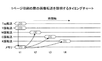
図4に示す画像転送ユニット40において、DFE2から送られてくる画像データの転送の様子を図5(1ページ印刷)に、3ページ印刷の様子を図6に、概略タイミングチャートとして示す。
[Transfer timing]
In the
図5に示す1ページ印刷の場合を用いて、転送のタイミングについてまず説明する。Y版と同タイミングで転送されるTagデータは、TagライトDMAC413によって、そのまま画像転送ユニット40内部のメモリであるTagバッファメモリ421(下記、単にメモリ421と示す)へ書き込まれる。それと同時にTagデータはY版の画像処理にも使用される。
First, the transfer timing will be described using the case of one-page printing shown in FIG. The Tag data transferred at the same timing as the Y version is directly written by the Tag write DMAC413 to the Tag buffer memory 421 (hereinafter, simply referred to as memory 421) which is a memory inside the
その後時間が経過し、M版の画像データの転送が開始されると(図5、時刻t2)、TagリードDMAC414Mにて、先程ライトされたTagデータのリードが開始される。リードされたTagデータはM版の画像データと同期を合わせてリードされ、画像処理を行っていく。その後のC版、K版も同様に行われる。 After that, when the time elapses and the transfer of the M version of the image data is started (FIG. 5, time t2), the tag read DMAC414M starts reading the previously written Tag data. The read Tag data is read in synchronization with the image data of the M version, and image processing is performed. Subsequent C and K versions are also performed in the same manner.
ここでは、4色について説明したが、色要素は、他の数であってもよい。例えば、Tag受信部であるTag受信回路411は、外部コントローラであるDFE2から複数のn色のTag情報を1ページに1回受信する。この際、図5に示すように、複数のn色のうちのいずれか一色の版の多値画像データを受信するタイミングは、Tag受信回路411がTag情報を受信するタイミングと同時である。
Although four colors have been described here, the number of color elements may be other. For example, the
TagライトDMAC413は、受信したTag情報のうちの前記一色以外の(n−1)色に対し、データの有効領域以外にページを識別するプロセス識別子を埋め込んで、メモリ421に蓄積させ、前記(n−1)色の各版の多値画像データを受信する夫々のタイミングで、メモリ42から蓄積したTag情報を読み出し、識別子を抽出して出力する。
The Tag Lite DMAC413 embeds a process identifier that identifies a page other than the effective area of data for a (n-1) color other than the one color in the received Tag information, stores it in the
図6の3ページ印刷のタイミングチャートでは、メカレイアウトによるが、本実施例では、2ページ目のY版の転送(2)が、M版の1ページ目の転送(1)と重なるタイミングとなる。さらにK版の1ページ目ではM版の3ページ目とC版の2ページ目と重なるタイミングとなる。一旦、メモリ421にライトされたTagデータは随時読み出されることになる。連続印刷になると、このような転送の重なりができるため、画像のハンドリングが複雑となる。
In the timing chart for printing three pages in FIG. 6, although it depends on the mechanical layout, in this embodiment, the transfer (2) of the Y version of the second page overlaps with the transfer (1) of the first page of the M version. .. Furthermore, the first page of the K version overlaps with the third page of the M version and the second page of the C version. The Tag data once written to the
加えて、4つの版が必ずあると限らず、印刷ページによっては、特定の版(例えばY版)が印刷データとして存在しないこともあるため、画像ハンドリングとしては複雑度が増してしまう。 In addition, there are not always four plates, and depending on the print page, a specific plate (for example, Y plate) may not exist as print data, which increases the complexity of image handling.
しかし、本発明では、下記制御のTagライトDMAC413及びTagリードDMAC414を適用することで、プロセスIDを判別し、適切に画像ハンドリングを実施させる。 However, in the present invention, by applying the Tag write DMAC413 and the Tag read DMAC414 of the following controls, the process ID is determined and image handling is appropriately performed.
[TagライトDMAC]
図7には図4に示すTagライトDMAC413の内部構成図を示し、以下に説明する。図7に示すように、TagライトDMAC413は、データ入力回路51、バスI/F回路52、プロセスID設定部53及びプロセスID埋め込み回路54を含む。
[Tag Light DMAC]
FIG. 7 shows an internal configuration diagram of the Tag Light DMAC413 shown in FIG. 4, which will be described below. As shown in FIG. 7, the Tag Lite DMAC413 includes a
TagライトDMAC413は、CPU44(図2参照)と接続されるCPUバス440からアクセスする開始アドレスを指定して起動される。その起動の際に、転送するプロセスIDを予め設定する。
The Tag write DMAC413 is started by designating a start address to be accessed from the
ここで、プロセスIDは、プロセス(ページ)を実行するための識別子(プロセス識別子、PID)であって、処理するページの固有番号(例えば、0から255の番号を繰り返し使う)を示す。 Here, the process ID is an identifier (process identifier, PID) for executing the process (page), and indicates a unique number of the page to be processed (for example, a number from 0 to 255 is repeatedly used).
起動後は、TagライトDMAC413では、データ入力回路51は、DFE2からのTagデータ受信に伴い、バスI/F回路52及びメモリバス420を介して、データをメモリ42内へ随時ライトする動作を行う。その際に、プロセスIDをライトするデータの中に埋め込むことを行うのがプロセスID埋め込み回路54である。具体的には印字有効領域より広い範囲をメモリの書き込み対象として、その印字有効範囲外の領域にプロセスIDを埋め込み、メモリ42にライトする(書き込む)。
After activation, in the Tag write DMAC413, the
図8に主走査の後部のラインに余白を作りラスタデータを埋め込む例を示す。画像の転送は主走査方向にラスタ形式で行われ、そのラスタデータは副走査方向にカウントするとラインと呼ばれる。そのラインの後部に余白部分を作り、その部分にプロセスIDを埋め込む。 FIG. 8 shows an example in which a margin is created in the rear line of the main scan and raster data is embedded. Image transfer is performed in raster format in the main scanning direction, and the raster data is called a line when counted in the sub-scanning direction. Create a margin at the back of the line and embed the process ID in that part.
また、図9に、副走査方向の後部のラインに余白を作りラスタデータを埋め込む例を示す。なお、埋め込む部分は、予め決められた余白であればどの位置であってもよい。 Further, FIG. 9 shows an example in which a margin is created in the rear line in the sub-scanning direction and raster data is embedded. The portion to be embedded may be at any position as long as it has a predetermined margin.
このように印字有効領域外にプロセスIDをデータとして埋め込むことにより、DMA転送を指示したデータが、所望のデータなのか判別可能となり、デバッグが容易となる。 By embedding the process ID as data outside the print effective area in this way, it becomes possible to determine whether the data instructing the DMA transfer is the desired data, and debugging becomes easy.
また、夫々の色ごとに異なるタイミングで画像処理へ移行させることで、色ごとに異なるタイミングで、画像ハンドリングをすることができる。 Further, by shifting to image processing at different timings for each color, image handling can be performed at different timings for each color.
したがって、その後の画像形成において、正しいデータを、色ごとに適切なタイミングで実施できるため、画像形成エンジンで用紙P上に作成される画像は、ページ毎にズレのない、正確なハンドリングにより、高品質となり、高速な画像形成に対応できる。 Therefore, in the subsequent image formation, correct data can be executed at an appropriate timing for each color, so that the image created on the paper P by the image formation engine is high due to accurate handling without deviation for each page. It becomes quality and can support high-speed image formation.
[TagリードDMAC]
図10には図4で説明のTagリードDMAC414の内部構成図を示し、以下に説明する。なお、図10では一例としてTagリードDMAC414Mを例として説明するが、TagリードDMAC414C,414Kも同様の構成であるため、説明を省略する。
[Tag read DMAC]
FIG. 10 shows an internal configuration diagram of the Tag read DMAC414 described with reference to FIG. 4, and will be described below. In FIG. 10, the Tag read DMAC414M will be described as an example, but since the Tag read DMAC414C and 414K also have the same configuration, the description thereof will be omitted.
図10に示すように、TagリードDMAC414Mは、バスI/F回路61、データ出力回路62、プロセスID設定部63、プロセスID抽出回路64及びプロセスID比較/割込み回路65を含む。
As shown in FIG. 10, the Tag read DMAC414M includes a bus I /
TagリードDMAC414Mでは、プロセスID設定部63がCPUバス440からアクセスする開始アドレスを指定して起動される。その起動の際に、転送するプロセスIDをあらかじめ設定する。
In the Tag read DMAC414M, the process
起動後、TagリードDMAC414Mでは、バスI/F回路61及びメモリバス420を介して、メモリ42から転送データをリードする(読み出す)動作を行う。読み出したリードデータの中から、TagライトDMAC413のプロセスIDの埋め込み箇所と同じ位置からプロセスIDの抽出をプロセスID抽出回路64にて行う。
After activation, the Tag read DMAC414M performs an operation of reading (reading) transfer data from the
プロセスID比較/割込み回路65では、抽出されたプロセスIDと、あらかじめ設定されたプロセスIDとを比較し、異なる場合に割込みを発生させる。割込みはFPGA41内部の割込み制御回路418(図4参照)にて処理され、CPU44に伝達される。
The process ID comparison / interrupt
これによって、CPU44は異常な動作をすぐに検出することができ、高品質な画像形成装置を提供することができる。また、識別子(プロセスID)の照合をFPGA41のハードウェア内で行うので、デバッグが容易になる。
As a result, the
[第2実施形態の画像転送ユニット]
図11に、本発明の第2実施形態に係る画像転送ユニット40AのFPGA41Aのブロック図を示す。図11に示す本実施形態に係るFPGA41Aは、図4に示す構成要素に加えて、少値画像データ用バッファメモリ422が設けられ、FPGA41Aは、各色版の画像ライトDMAC491Y,491M,491C,491K、各色版の画像リードDMAC492Y,492M,492C,492Kをさらに備えている。
[Image transfer unit of the second embodiment]
FIG. 11 shows a block diagram of
少値画像データ用バッファメモリ(第2のバッファメモリ、メモリ)422は、画像処理後の少値画像データ用のバッファメモリであって、各色の版ごとに表面印字用としてページ2面、裏面印字用としてページ2面の計4面を有している。 The buffer memory for low-value image data (second buffer memory, memory) 422 is a buffer memory for low-value image data after image processing, and is printed on two pages and back side for front side printing for each color plate. It has a total of 4 pages, 2 pages for use.
各版の画像ライトDMAC491Y,491M,491C,491K及び各版の画像リードDMAC492Y,492M,492C,492Kは、CPU44とCPUバス440を介して接続されている。
The image lights DMAC491Y, 491M, 491C, 491K of each version and the image reads DMAC492Y, 492M, 492C, 492K of each version are connected to the
Y版ライトDMAC(画像ライトDMA部)491Yは、少値化後の画像データをメモリ422にライトするDMA回路である。あらかじめ第2のメモリ422をアクセスする開始アドレスがCPU44にて設定される。画像ライトDMAC491M,491C,491Kでの、他の色版でも同様である。
The Y version light DMAC (image light DMA unit) 491Y is a DMA circuit that writes the image data after the reduction in value to the
Y版リードDMAC(画像リードDMA部)492Yは、印刷要求に合わせて起動されるK版データを転送するDMA回路である。あらかじめ第2のメモリ422をアクセスする開始アドレスがCPU44にて設定されている。画像リードDMAC492M,492C,492Kでの、他の色版でも同様である。
The Y-plate read DMAC (image read DMA unit) 492Y is a DMA circuit that transfers K-plate data that is activated in response to a print request. The start address for accessing the
上述のように、本実施形態では、少値化後のデータを、一旦画像転送ユニット40Aの第2のメモリ422に蓄積する点が、図4の制御とは異なる。本実施形態では、このように一旦蓄積することで、印字のためのデータ転送速度に、DFE2からのデータ受信速度を緩和すること可能になる。
As described above, the present embodiment is different from the control of FIG. 4 in that the data after the reduction in value is temporarily stored in the
印字側のデータ転送速度は搬送される転写紙と次の転写紙の間の時間(紙間とも呼ばれる)を含まない期間に行われるため、DFE2側の転送速度に比べて、その分だけ速くする必要がある。 Since the data transfer speed on the printing side does not include the time between the transferred transfer paper and the next transfer paper (also called the paper spacing), the data transfer speed on the DFE2 side is increased by that amount. There is a need.
なお、各版のライトDMAC491Y,491M,491C,491Kの内部構成は、図7に示すTagライトDMAC413と同様である。この場合、用途がTag情報と、色ごとの版の少値画像データとで異なるが、データのプロセスIDを、第2のメモリ422にライトする点で同様である。
The internal configuration of each version of the light DMAC491Y, 491M, 491C, 491K is the same as that of the Tag light DMAC413 shown in FIG. In this case, the usage differs between the Tag information and the low-value image data of the plate for each color, but it is the same in that the process ID of the data is written to the
また、上記各版リードDMAC492Y,492M,492C,492Kの内部構成は、図10に示すTagリードDMAC414Mの構成と同様である。この場合、用途が色ごとの版の多値画像データと、色ごとの版の少値画像データとで異なるが、蓄積したデータのプロセスIDを、リード時に照合するという点で同様である。 Further, the internal configuration of each of the above-mentioned version read DMAC492Y, 492M, 492C, 492K is the same as the configuration of the Tag read DMAC414M shown in FIG. In this case, the usage differs between the multi-valued image data of the plate for each color and the low-value image data of the plate for each color, but it is the same in that the process ID of the accumulated data is collated at the time of reading.
このように、第2のメモリ422から読み出すTagデータでも、メモリアクセスの先頭アドレスをCPU44より指示して行うが、そのデータからハードウェアでライト時に埋め込んだ識別子を抽出することにより、正しいもしくは誤ったデータか判別できるため、デバッグが容易となる。
In this way, even in the Debug data read from the
したがって、画像転送ユニットの制御ソフトウェア作成時のデバッグにおいて、画像ハンドリングに関するミスが判別でき、設計効率が向上し、また高品質の画像形成装置の提供が可能となる。 Therefore, in debugging when creating control software for the image transfer unit, mistakes related to image handling can be discriminated, design efficiency is improved, and a high-quality image forming apparatus can be provided.
上述のように、本発明の複数の実施形態では、画像種を示すTag情報、及び画像処理後の画像データに対して、蓄積時にデータの有効領域以外の部分に、処理するページの固有番号を示すプロセスIDを埋め込み、所定のタイミングでそれらのデータを読み出した際にプロセスIDを取り出し、ソフトウェアで判別できるようにした。 As described above, in the plurality of embodiments of the present invention, with respect to the Tag information indicating the image type and the image data after image processing, the unique number of the page to be processed is set in a portion other than the effective area of the data at the time of storage. The indicated process ID is embedded, and when the data is read out at a predetermined timing, the process ID is taken out so that it can be identified by software.
これによって、DMA転送を指示したデータが所望のデータなのか判別可能となり、デバッグが容易となる。 As a result, it becomes possible to determine whether the data instructing the DMA transfer is the desired data, and debugging becomes easy.
なお、上記では、画像形成装置として、電子写真方式のカラープリンタの場合について説明したが、これに限定されるものではなく、例えば、光プロッタやデジタル複写装置であってもよい。あるいは、画像形成装置は、用紙にインクを吹き付けて画像を形成するインクジェットプリンタにも適用可能であってもよい。 In the above description, the case of an electrophotographic color printer as the image forming apparatus has been described, but the present invention is not limited to this, and for example, an optical plotter or a digital copying apparatus may be used. Alternatively, the image forming apparatus may be applicable to an inkjet printer that forms an image by spraying ink on paper.
また、上記の画像形成装置では、画像形成の対象を用紙として説明したが、画像が形成される記録媒体は、紙に限定されるものではない。例えば、記録媒体とは、液体が少なくとも一時的に付着可能なものであって、付着して固着するもの、付着して浸透するものなどを意味する。具体例としては、用紙、記録紙、記録用紙、フィルム、布などの被記録媒体、電子基板、圧電素子などの電子部品、粉体層(粉末層)、臓器モデル、検査用セルなどの媒体であり、特に限定しない限り、液体や粉体が付着するすべてのものが含まれる。例えば、上記「対象物」の材質は、紙、糸、繊維、布帛、皮革、金属、プラスチック、ガラス、木材、セラミックスなどであり、液体が一時的でも付着可能な材質であればよい。 Further, in the above-mentioned image forming apparatus, the object of image formation is described as paper, but the recording medium on which the image is formed is not limited to paper. For example, the recording medium means a medium to which a liquid can adhere at least temporarily, such as one that adheres and adheres, and one that adheres and permeates. Specific examples include paper, recording paper, recording paper, film, recording media such as cloth, electronic substrates, electronic components such as piezoelectric elements, powder layers (powder layers), organ models, and media such as inspection cells. Yes, including anything to which liquids and powders adhere, unless otherwise specified. For example, the material of the "object" is paper, thread, fiber, cloth, leather, metal, plastic, glass, wood, ceramics, or the like, and any material may be used as long as the liquid can be attached even temporarily.
以上、本発明の好ましい実施形態について詳述したが、本発明は係る特定の実施形態に限定されるものではなく、特許請求の範囲に記載された本発明の実施形態の要旨の範囲内において、種々の変形、変更が可能である。 Although the preferred embodiment of the present invention has been described in detail above, the present invention is not limited to the specific embodiment, and is within the scope of the gist of the embodiment of the present invention described in the claims. Various modifications and changes are possible.
1 画像形成装置
2 DFE(外部コントローラ、デジタルフロントエンド)
10 制御部
110 コントローラ(制御部)
120 IPU(制御部)
130 BCU(制御部)
20 操作部
30 画像形成エンジン
300 書き込み部
313 センサー
40,40A 画像転送ユニット(データ転送ユニット、DTU)
41,41A FPGA(画像転送用の集積回路)
42 RAM
44 CPU
411 Tag受信回路
412(412Y,412M,412C,412K) 多値画像データ受信回路(多値データ受信部)
412 Tag受信回路(Tag受信部)
413 TagライトDMAC(TagライトDMA部)
414(414M,414C,414K) TagリードDMAC(TagリードDMA部)
415 パラメータ送信部
416(416Y,416M,416C,416K) ディザ処理回路(画像処理部)
417(417Y,417M,417C,417K) エッジエンハンス回路(画像処理部)
418 割り込み制御回路
419 PCIeI/F回路
421 メモリ(Tagバッファメモリ、第1のメモリ)
422 メモリ (少値画像データ用バッファメモリ、第2のメモリ)
491 K版ライトDMAC(画像ライトDMA部)
492 K版リードDMAC(画像リードDMA部)
P 用紙(記録媒体)
Tag Tag情報(タグ)
PID プロセスID(プロセス識別子、開始アドレス)
1 Image forming
10
120 IPU (control unit)
130 BCU (control unit)
20
41,41A FPGA (Integrated circuit for image transfer)
42 RAM
44 CPU
411 Tag receiving circuit 412 (412Y, 412M, 412C, 412K) Multi-value image data receiving circuit (multi-value data receiving unit)
412 Tag receiver circuit (Tag receiver)
413 Tag light DMAC (Tag light DMA part)
414 (414M, 414C, 414K) Tag lead DMAC (Tag lead DMA section)
415 Parameter transmitter 416 (416Y, 416M, 416C, 416K) Dither processing circuit (image processing unit)
417 (417Y, 417M, 417C, 417K) Edge enhancement circuit (image processing unit)
418 Interrupt
422 memory (buffer memory for low-value image data, second memory)
491 K version light DMAC (image light DMA section)
492 K version read DMAC (image read DMA section)
P paper (recording medium)
Tag Tag information (tag)
PID Process ID (process identifier, start address)
Claims (7)
前記外部コントローラから複数の色ごとの版の多値画像データと、文字や写真等の画像種や属性を識別するTag情報とを受信し、前記多値画像データに対しTag情報に応じた画像処理を行う画像転送ユニット、
記録媒体に印刷動作を行う画像形成エンジン、及び
前記外部コントローラから印刷指示を受信し、前記画像転送ユニットから取得した前記各版の画像処理後の画像データを基に、前記画像形成エンジンの印刷動作を実行させるように制御する制御部を備えており、
前記画像転送ユニットは、
第1のメモリと、
前記外部コントローラから前記Tag情報を1ページに1回受信するTag受信部と、
受信した前記Tag情報に対し、データの有効領域以外に、ページを識別するためのプロセス識別子を埋め込み、前記第1のメモリに蓄積するTagライトDMA部と、
前記複数の色ごとの版の多値画像データを受信する夫々のタイミングで、蓄積した前記Tag情報を読み出し、前記プロセス識別子を抽出して、出力するTagリードDMA部と、
前記第1のメモリより読み出した前記Tag情報を利用して、受信した前記色ごとの版の多値画像データに対し画像処理を行う画像処理部と、を備え、
前記TagリードDMA部では、前記Tag情報から抽出したプロセス識別子に対し、所定の値であるかどうかを判定することを特徴とする
画像形成装置。 An image forming device connected to an external controller via an interface.
Receives multi-valued image data of a plurality of plates for each color from the external controller and Tag information for identifying image types and attributes such as characters and photographs, and performs image processing on the multi-valued image data according to the Tag information. image transfer unit for,
The image forming engine performs printing operation on a recording medium, and receives a print instruction from the external controller, based on the image picture data after the image processing of each plate obtained from the image transfer unit, the printing of the image forming engine It is equipped with a control unit that controls the operation to be executed.
The image transfer unit is
The first memory and
A Tag receiver that receives the Tag information from the external controller once per page, and
In the received Tag information, a Tag write DMA unit that embeds a process identifier for identifying a page in addition to the effective area of data and stores it in the first memory, and
A Tag read DMA unit that reads out the accumulated Tag information, extracts the process identifier, and outputs the tag information at each timing of receiving the multi-valued image data of the plates for each of the plurality of colors.
It is provided with an image processing unit that performs image processing on the received multi-valued image data of the plate for each color by using the Tag information read from the first memory.
The tag read DMA unit is an image forming apparatus characterized in that it determines whether or not the process identifier extracted from the tag information has a predetermined value.
第2のメモリと、
前記画像処理部により画像処理された画像データに対し、データの有効領域以外にページを識別するためのプロセス識別子を埋め込み、前記第2のメモリに蓄積する画像ライトDMA部と、
各版の画像処理後の画像データを前記第2のメモリから読み出し、前記プロセス識別子を抽出して出力する画像リードDMA部を備え、
前記画像リードDMA部では、前記画像データから抽出したプロセス識別子に対し、第2の所定の値であるかどうかを判定することを特徴とする
請求項1に記載の画像形成装置。 The image transfer unit is
The second memory and
An image light DMA unit that embeds a process identifier for identifying a page other than the effective area of the data in the image data image-processed by the image processing unit and stores the image data in the second memory.
An image read DMA unit that reads image data after image processing of each version from the second memory, extracts the process identifier, and outputs the process identifier is provided.
The image forming apparatus according to claim 1, wherein the image read DMA unit determines whether or not the process identifier extracted from the image data has a second predetermined value.
請求項1又は2に記載の画像形成装置。 According to claim 1 or 2, the Tag read DMA unit collates each read process identifier with a preset predetermined value, and if they are different, an error interrupt is generated. The image forming apparatus described.
前記Tag受信部は、前記外部コントローラから複数のn色のTag情報を1ページに1回受信し、
前記複数のn色のうちのいずれか一色の版の多値画像データを受信するタイミングは、前記Tag受信部が前記Tag情報を受信するタイミングと同時であり、
前記TagライトDMA部は、前記受信したTag情報のうちの前記一色以外の(n−1)色に対し、データの有効領域以外にページを識別するための識別子を埋め込んで、前記第1のメモリに蓄積させ、
前記TagリードDMA部は、前記(n−1)色の各版の多値画像データを受信する夫々のタイミングで、前記第1のメモリから蓄積した前記Tag情報を読み出し、前記識別子を抽出して出力することを特徴とする
請求項1乃至3のいずれか一項に記載の画像形成装置。 It is provided with n multi-value image data receivers corresponding to n colors, which are two or more integers that receive multi-value image data of plates for each of the plurality of colors from the external controller.
The Tag receiving unit receives a plurality of n-color Tag information from the external controller once per page.
The timing of receiving the multi-valued image data of the plate of any one of the plurality of n colors is the same as the timing of receiving the Tag information by the Tag receiving unit.
The Tag light DMA unit embeds an identifier for identifying a page other than the effective area of data for a (n-1) color other than the one color in the received Tag information, and the first memory. Accumulate in
The Tag read DMA unit reads the Tag information accumulated from the first memory at each timing of receiving the multi-valued image data of each version of the (n-1) color, and extracts the identifier. The image forming apparatus according to any one of claims 1 to 3, wherein the image forming apparatus is characterized by outputting.
請求項1乃至4のいずれか一項に記載の画像形成装置。 The image forming apparatus according to any one of claims 1 to 4.
前記デジタルフロントエンドとインターフェースを介して接続される請求項1乃至5のいずれか一項に記載の画像形成装置と、を備えることを特徴とする
印刷システム。 A digital front end that functions as the external controller that receives print data sent from the user, draws it, and creates multi-valued image data.
A printing system comprising the image forming apparatus according to any one of claims 1 to 5 , which is connected to the digital front end via an interface.
前記外部コントローラから、文字や写真等の画像種を識別するTag情報を1ページに1回受信するTag受信部と、
受信した前記Tag情報に対し、データの有効領域以外にページを識別するための識別子を埋め込んで、前記メモリに蓄積させるTagライトDMA部と、
複数の色ごとの版の多値画像データを受信する夫々のタイミングで、前記メモリから蓄積した前記Tag情報を読み出し、前記識別子を抽出して出力するTagリードDMA部と、
前記メモリより読み出した前記Tag情報を利用して、受信した前記色ごとの版の多値画像データに対し画像処理を行う画像処理部と、を備え、
前記TagリードDMA部では、読み出された識別子に対し、所定の値であるかどうかを判定することを特徴とする
画像転送用の集積回路。 An integrated circuit for image transfer connected to a memory that can be mounted on an image forming device connected to an external controller via an interface.
A Tag receiver that receives Tag information that identifies an image type such as a character or a photograph once per page from the external controller.
A Tag write DMA unit that embeds an identifier for identifying a page other than the effective area of data in the received Tag information and stores it in the memory.
A Tag read DMA unit that reads the Tag information accumulated from the memory at each timing of receiving the multi-valued image data of a plurality of color plates, extracts the identifier, and outputs the identifier.
It is provided with an image processing unit that performs image processing on the received multi-valued image data of the plate for each color by using the Tag information read from the memory.
The Tag read DMA unit is an integrated circuit for image transfer, characterized in that it determines whether or not the read identifier has a predetermined value.
Priority Applications (1)
| Application Number | Priority Date | Filing Date | Title |
|---|---|---|---|
| JP2016186228A JP6766552B2 (en) | 2016-09-23 | 2016-09-23 | Image forming equipment, printing system and integrated circuit for image transfer |
Applications Claiming Priority (1)
| Application Number | Priority Date | Filing Date | Title |
|---|---|---|---|
| JP2016186228A JP6766552B2 (en) | 2016-09-23 | 2016-09-23 | Image forming equipment, printing system and integrated circuit for image transfer |
Publications (2)
| Publication Number | Publication Date |
|---|---|
| JP2018047675A JP2018047675A (en) | 2018-03-29 |
| JP6766552B2 true JP6766552B2 (en) | 2020-10-14 |
Family
ID=61767068
Family Applications (1)
| Application Number | Title | Priority Date | Filing Date |
|---|---|---|---|
| JP2016186228A Active JP6766552B2 (en) | 2016-09-23 | 2016-09-23 | Image forming equipment, printing system and integrated circuit for image transfer |
Country Status (1)
| Country | Link |
|---|---|
| JP (1) | JP6766552B2 (en) |
-
2016
- 2016-09-23 JP JP2016186228A patent/JP6766552B2/en active Active
Also Published As
| Publication number | Publication date |
|---|---|
| JP2018047675A (en) | 2018-03-29 |
Similar Documents
| Publication | Publication Date | Title |
|---|---|---|
| US8964249B2 (en) | Image test apparatus, image test system, and image test method for testing a print image based on master image data | |
| JP6852430B2 (en) | Inspection equipment, inspection methods and programs | |
| AU2012216252B2 (en) | Printing system, image inspecting apparatus, and printing method | |
| EP2879366B1 (en) | Document reading device and image forming apparatus | |
| JP2016061659A (en) | Printed matter inspection apparatus, printed matter inspection system, and printed matter inspection method | |
| US9223244B2 (en) | Image writing device, image forming apparatus, and image writing method | |
| US8456652B2 (en) | Image forming apparatus and method for controlling sheet conveyance intervals in same | |
| JP2016055525A (en) | Defect information identification device and defect information identification method | |
| JP2018044896A (en) | Inspection apparatus, inspection method and program | |
| US9030691B2 (en) | Printing system, printing method, and recording medium | |
| US8885226B2 (en) | Image forming apparatus | |
| JP5046844B2 (en) | Image forming apparatus and image forming program | |
| US9001358B2 (en) | Image forming system | |
| JP2013251611A (en) | Image processing apparatus, control method of the same, and program | |
| JP4834571B2 (en) | Image forming system, control method therefor, and information processing apparatus | |
| JP6766552B2 (en) | Image forming equipment, printing system and integrated circuit for image transfer | |
| US8854646B2 (en) | Printing device and control method of printing device | |
| JP6497242B2 (en) | Image forming apparatus, image forming method, and image forming system | |
| JP6489302B2 (en) | Image forming apparatus and data transmission method | |
| JP6852540B2 (en) | Image forming apparatus, printing system, and integrated circuit for image transfer mounted on the image forming apparatus | |
| JP6047084B2 (en) | Image forming apparatus | |
| JP7298281B2 (en) | Image forming apparatus, image forming method, image forming program | |
| JPH10285385A (en) | Image processing system and apparatus and method, and storage medium | |
| JP3544021B2 (en) | Image processing apparatus and method | |
| JP2002323805A (en) | Color image forming equipment |
Legal Events
| Date | Code | Title | Description |
|---|---|---|---|
| A621 | Written request for application examination |
Free format text: JAPANESE INTERMEDIATE CODE: A621 Effective date: 20190703 |
|
| A977 | Report on retrieval |
Free format text: JAPANESE INTERMEDIATE CODE: A971007 Effective date: 20200520 |
|
| A131 | Notification of reasons for refusal |
Free format text: JAPANESE INTERMEDIATE CODE: A131 Effective date: 20200602 |
|
| A521 | Written amendment |
Free format text: JAPANESE INTERMEDIATE CODE: A523 Effective date: 20200803 |
|
| TRDD | Decision of grant or rejection written | ||
| A01 | Written decision to grant a patent or to grant a registration (utility model) |
Free format text: JAPANESE INTERMEDIATE CODE: A01 Effective date: 20200818 |
|
| A61 | First payment of annual fees (during grant procedure) |
Free format text: JAPANESE INTERMEDIATE CODE: A61 Effective date: 20200831 |
|
| R151 | Written notification of patent or utility model registration |
Ref document number: 6766552 Country of ref document: JP Free format text: JAPANESE INTERMEDIATE CODE: R151 |