JP6754786B2 - Transfer circuits, shift registers, gate drivers, display panels, and flexible boards - Google Patents
Transfer circuits, shift registers, gate drivers, display panels, and flexible boards Download PDFInfo
- Publication number
- JP6754786B2 JP6754786B2 JP2018001893A JP2018001893A JP6754786B2 JP 6754786 B2 JP6754786 B2 JP 6754786B2 JP 2018001893 A JP2018001893 A JP 2018001893A JP 2018001893 A JP2018001893 A JP 2018001893A JP 6754786 B2 JP6754786 B2 JP 6754786B2
- Authority
- JP
- Japan
- Prior art keywords
- output
- circuit
- transistor
- input
- transfer circuit
- Prior art date
- Legal status (The legal status is an assumption and is not a legal conclusion. Google has not performed a legal analysis and makes no representation as to the accuracy of the status listed.)
- Active
Links
Images


Classifications
-
- G—PHYSICS
- G09—EDUCATION; CRYPTOGRAPHY; DISPLAY; ADVERTISING; SEALS
- G09G—ARRANGEMENTS OR CIRCUITS FOR CONTROL OF INDICATING DEVICES USING STATIC MEANS TO PRESENT VARIABLE INFORMATION
- G09G3/00—Control arrangements or circuits, of interest only in connection with visual indicators other than cathode-ray tubes
- G09G3/20—Control arrangements or circuits, of interest only in connection with visual indicators other than cathode-ray tubes for presentation of an assembly of a number of characters, e.g. a page, by composing the assembly by combination of individual elements arranged in a matrix no fixed position being assigned to or needed to be assigned to the individual characters or partial characters
- G09G3/22—Control arrangements or circuits, of interest only in connection with visual indicators other than cathode-ray tubes for presentation of an assembly of a number of characters, e.g. a page, by composing the assembly by combination of individual elements arranged in a matrix no fixed position being assigned to or needed to be assigned to the individual characters or partial characters using controlled light sources
- G09G3/30—Control arrangements or circuits, of interest only in connection with visual indicators other than cathode-ray tubes for presentation of an assembly of a number of characters, e.g. a page, by composing the assembly by combination of individual elements arranged in a matrix no fixed position being assigned to or needed to be assigned to the individual characters or partial characters using controlled light sources using electroluminescent panels
- G09G3/32—Control arrangements or circuits, of interest only in connection with visual indicators other than cathode-ray tubes for presentation of an assembly of a number of characters, e.g. a page, by composing the assembly by combination of individual elements arranged in a matrix no fixed position being assigned to or needed to be assigned to the individual characters or partial characters using controlled light sources using electroluminescent panels semiconductive, e.g. using light-emitting diodes [LED]
- G09G3/3208—Control arrangements or circuits, of interest only in connection with visual indicators other than cathode-ray tubes for presentation of an assembly of a number of characters, e.g. a page, by composing the assembly by combination of individual elements arranged in a matrix no fixed position being assigned to or needed to be assigned to the individual characters or partial characters using controlled light sources using electroluminescent panels semiconductive, e.g. using light-emitting diodes [LED] organic, e.g. using organic light-emitting diodes [OLED]
- G09G3/3266—Details of drivers for scan electrodes
-
- G—PHYSICS
- G09—EDUCATION; CRYPTOGRAPHY; DISPLAY; ADVERTISING; SEALS
- G09G—ARRANGEMENTS OR CIRCUITS FOR CONTROL OF INDICATING DEVICES USING STATIC MEANS TO PRESENT VARIABLE INFORMATION
- G09G3/00—Control arrangements or circuits, of interest only in connection with visual indicators other than cathode-ray tubes
- G09G3/20—Control arrangements or circuits, of interest only in connection with visual indicators other than cathode-ray tubes for presentation of an assembly of a number of characters, e.g. a page, by composing the assembly by combination of individual elements arranged in a matrix no fixed position being assigned to or needed to be assigned to the individual characters or partial characters
- G09G3/34—Control arrangements or circuits, of interest only in connection with visual indicators other than cathode-ray tubes for presentation of an assembly of a number of characters, e.g. a page, by composing the assembly by combination of individual elements arranged in a matrix no fixed position being assigned to or needed to be assigned to the individual characters or partial characters by control of light from an independent source
- G09G3/36—Control arrangements or circuits, of interest only in connection with visual indicators other than cathode-ray tubes for presentation of an assembly of a number of characters, e.g. a page, by composing the assembly by combination of individual elements arranged in a matrix no fixed position being assigned to or needed to be assigned to the individual characters or partial characters by control of light from an independent source using liquid crystals
- G09G3/3611—Control of matrices with row and column drivers
- G09G3/3648—Control of matrices with row and column drivers using an active matrix
-
- G—PHYSICS
- G11—INFORMATION STORAGE
- G11C—STATIC STORES
- G11C19/00—Digital stores in which the information is moved stepwise, e.g. shift registers
- G11C19/28—Digital stores in which the information is moved stepwise, e.g. shift registers using semiconductor elements
-
- G—PHYSICS
- G09—EDUCATION; CRYPTOGRAPHY; DISPLAY; ADVERTISING; SEALS
- G09G—ARRANGEMENTS OR CIRCUITS FOR CONTROL OF INDICATING DEVICES USING STATIC MEANS TO PRESENT VARIABLE INFORMATION
- G09G2310/00—Command of the display device
- G09G2310/02—Addressing, scanning or driving the display screen or processing steps related thereto
- G09G2310/0264—Details of driving circuits
- G09G2310/0286—Details of a shift registers arranged for use in a driving circuit
Description
本発明は、転送回路、シフトレジスタ、ゲートドライバ、表示パネル、およびフレキシブル基板に関する。 The present invention relates to transfer circuits, shift registers, gate drivers, display panels, and flexible substrates.
従来、複数の画素回路をマトリクス状に配置してなる表示装置が広く実用化されている。そのような表示装置では、複数の画素回路を、行ごとに異なるタイミングの制御信号を用いて、行順次に駆動することによって、映像を表示している。行ごとの制御信号は、例えば、シフトレジスタを用いて生成される。特許文献1には、そのようなシフトレジスタの各段の転送回路として利用することができるレジスタ回路が開示されている。
Conventionally, a display device in which a plurality of pixel circuits are arranged in a matrix has been widely put into practical use. In such a display device, an image is displayed by driving a plurality of pixel circuits in sequence using control signals having different timings for each row. The line-by-line control signal is generated using, for example, a shift register.
特許文献1に開示されるレジスタ回路では、本来なら低電位側にあるべき出力信号の電位が、わずかながら上昇する場合がある。そのため、当該レジスタ回路を複数接続してなるシフトレジスタでは、制御信号の転送を繰り返すうちに電位の上昇が積み重なり、誤動作が発生する懸念がある。
In the register circuit disclosed in
そこで、本発明は、出力信号に非所望の電位上昇が起こりにくい転送回路、およびそのような転送回路を用いたシフトレジスタ、ゲートドライバ、表示パネル、およびフレキシブル基板を提供することを目的とする。 Therefore, an object of the present invention is to provide a transfer circuit in which an undesired potential rise is unlikely to occur in an output signal, and a shift register, a gate driver, a display panel, and a flexible substrate using such a transfer circuit.
上記目的を達成するために、本発明の1つの態様に係る転送回路は、入力回路、リセット回路、出力回路、出力安定化回路から構成され、クロック信号に同期して、入力端にて入力信号を取得して保持し、保持された入力信号を出力信号として出力端から出力する転送回路において、前記出力安定化回路は、前記転送回路の前記入力端および前記出力端のうちのいずれか一方または両方に接続され、前記入力信号および前記出力信号の少なくとも一方の極性を反転した反転信号を出力端から出力する反転回路と、前記反転回路の前記出力端が制御信号端に接続され、第1の主信号端が前記出力安定化回路の電源である第1の電源に接続され、第2の主信号端が前記転送回路の前記出力端に接続されている第1のトランジスタと、を含む。 In order to achieve the above object, the transfer circuit according to one aspect of the present invention is composed of an input circuit, a reset circuit, an output circuit, and an output stabilizing circuit, and is synchronized with a clock signal and has an input signal at an input terminal. In a transfer circuit that acquires and holds an input signal and outputs the held input signal as an output signal from the output end, the output stabilization circuit is one of the input end and the output end of the transfer circuit, or A first inversion circuit which is connected to both and outputs an inverting signal in which the polarity of at least one of the input signal and the output signal is inverted is output from the output end, and the output end of the inverting circuit is connected to the control signal end. Includes a first transistor whose main signal end is connected to a first power source, which is the power source for the output stabilization circuit, and whose second main signal end is connected to the output end of the transfer circuit.
このような構成によれば、反転信号は、転送回路の入力信号および出力信号の少なくとも一方が低電位側にあるときに高電位側の電位となって第1のトランジスタをオン状態にする。これにより、転送回路の出力が低電位側にあるべきときに、転送回路の出力端は第1の電源に接続されるので、転送回路の出力の電位の上昇が抑制される。 According to such a configuration, the inverting signal becomes a potential on the high potential side when at least one of the input signal and the output signal of the transfer circuit is on the low potential side, and turns on the first transistor. As a result, when the output of the transfer circuit should be on the low potential side, the output end of the transfer circuit is connected to the first power source, so that the increase in the potential of the output of the transfer circuit is suppressed.
このような転送回路を複数接続してなるシフトレジスタでは、制御信号の転送を繰り返しても電位の上昇が積み重なりにくくなり、誤動作の発生が防止される。 In a shift register in which a plurality of such transfer circuits are connected, even if the transfer of control signals is repeated, the potential rises are less likely to accumulate, and the occurrence of malfunction is prevented.
(本発明の基礎となった知見)
本発明の実施の形態について説明する前に、従来例に係るレジスタ回路の動作、および、本発明者によって見出された誤動作の可能性について説明する。
(Knowledge that became the basis of the present invention)
Before explaining the embodiment of the present invention, the operation of the register circuit according to the conventional example and the possibility of malfunction found by the present inventor will be described.
図1は、一般的な表示装置の要部の構成の一例を示す機能ブロック図である。図1に示されるように、表示装置1の要部は、複数の画素回路10、ライトスキャナ21、行電源スキャナ22、水平セレクタ23、走査信号線31、32、およびデータ信号線33で構成されている。
FIG. 1 is a functional block diagram showing an example of the configuration of a main part of a general display device. As shown in FIG. 1, the main part of the
複数の画素回路10は、マトリクス状に配置されている。当該マトリクスの各行には同じ行に配置される複数の画素回路10に共通に接続される走査信号線31、32が設けられ、当該マトリクスの各列には同じ列に配置される複数の画素回路10に共通に接続されるデータ信号線33が設けられる。
The plurality of
ライトスキャナ21および行電源スキャナ22は、走査信号線31、32を介して、画素回路10に、行ごとのタイミングで画素回路10の動作を制御するための書込み信号および行電源をそれぞれ供給する。
The
水平セレクタ23は、データ信号線33を介して、画素回路10に、輝度に対応するデータ信号を供給する。
The
図2は、従来例に係る画素回路の構成の一例を示す回路図であり、アクティブマトリクス型有機EL表示装置における画素回路の例を示している。 FIG. 2 is a circuit diagram showing an example of the configuration of the pixel circuit according to the conventional example, and shows an example of the pixel circuit in the active matrix type organic EL display device.
有機EL素子は電流発光素子のため、有機EL素子に流れる電流量をコントロールすることで発色の階調を得ている。図2の画素回路では、スイッチングトランジスタTsを介して保持容量Csに保持したデータ電圧に応じた量の電流を、駆動トランジスタTdからEL素子へ供給している。 Since the organic EL element is a current light emitting element, the gradation of color development is obtained by controlling the amount of current flowing through the organic EL element. In the pixel circuit of FIG. 2, a current corresponding to the data voltage held in the holding capacitance Cs is supplied from the driving transistor Td to the EL element via the switching transistor Ts.
図3は、表示装置1の動作の一例を示すタイミングチャートであり、隣接する2行に位置する画素回路10に供給される書込み信号、行電源、およびデータ信号の時間波形の一例を示している。図3において符号の末尾に付与されているかっこ書きの数字は、対応する行番号を意味している。
FIG. 3 is a timing chart showing an example of the operation of the
画素回路10は、図3に示される波形の書込み信号および行電源を供給されることにより、先行するフレームの発光終了後、4水平同期(H)期間をかけて、閾値補正準備、閾値補正、書込みおよび移動度補正を行い、後続のフレームの発光を開始する。なお、画素回路10の構成および動作の詳細は、本発明の要部ではないため、周知の技術を適宜用いるものとして説明を省略する。
By supplying the write signal and line power of the waveform shown in FIG. 3, the
ライトスキャナ21および行電源スキャナ22が、行ごとにずれたタイミングで書込み信号および行電源を供給することで、画素回路10での発光、閾値補正準備、閾値補正、書込みおよび移動度補正動作は、行ごとに異なるタイミング(例えば、1水平同期時間ずつずれたタイミング)で実行される。
The
ライトスキャナ21および行電源スキャナ22は、ドライバICに設けられてもよく、コストの削減のために表示パネルに内蔵されてもよい。ライトスキャナ21や行電源スキャナ22のように、同じ波形の複数の信号を、ずれたタイミングで出力するスキャナ回路は、例えば、シフトレジスタを用いて構成することができる。
The
図4は、スキャナ回路20の概略構成の一例を示す機能ブロック図であり、ライトスキャナ21および行電源スキャナ22のいずれにも適用され得る汎用的な回路構成の一部を示している。スキャナ回路20は、複数の転送回路100を連ねて構成されるシフトレジスタ700と、転送回路100の出力に応じて出力信号線900を駆動する複数のバッファ回路800とで構成される。転送回路100、バッファ回路800、および出力信号線900は、表示装置1の行に対応して設けられる。シフトレジスタ700は、一例として、アクティブな期間が重複しない3相のクロック信号CK1、CK2、CK3に従って動作する3相駆動のシフトレジスタである。
FIG. 4 is a functional block diagram showing an example of a schematic configuration of the
周辺駆動回路や画素回路において、一般には低コスト化のためにLTPS(低温ポリシリコン)−TFT(Thin Film Transistor)よりもプロセスが簡略化されているaSi(アモルファスシリコン)―TFTや酸化物TFTを用いることが多い。しかしながらaSi―TFTや酸化物TFTはLTPS―TFTと異なり、回路を構成するトランジスタの極性がNchトランジスタのみしか存在しないために駆動回路が複雑になってしまう。 In peripheral drive circuits and pixel circuits, aSi (amorphous silicon) -TFTs and oxide TFTs, whose processes are generally simpler than LTPS (low temperature polysilicon) -TFTs (Thin Film Transistors) for cost reduction, are used. Often used. However, unlike the LTPS-TFT, the aSi-TFT and the oxide TFT have a complicated drive circuit because the polarities of the transistors constituting the circuit are only Nch transistors.
近年、作成の容易さに加え低リーク、高移動度といった特性から酸化物TFTが着目されている。しかし酸化物TFTは前述のようにNchトランジスタのみしか存在しないことに加え、一般に閾値電圧が負(デプレッション型)であるため、周辺駆動回路においてTFTの閾値電圧が負であっても誤動作を起こさないようにする必要がある。 In recent years, oxide TFTs have been attracting attention because of their characteristics such as low leakage and high mobility in addition to ease of production. However, since the oxide TFT has only the Nch transistor as described above and the threshold voltage is generally negative (depression type), no malfunction occurs even if the threshold voltage of the TFT is negative in the peripheral drive circuit. Must be done.
シフトレジスタ700の各段の転送回路100には、例えば、特許文献1のレジスタ回路を利用することができる。
For the
図5は、転送回路100の構成の一例を示す回路図であり、特許文献1の図13に挙げられているレジスタ回路を示している。図中の符号は適宜変更されている。以下の説明では、簡潔のため、信号と、信号を入出力するための端子とを、同一の符号で参照する。
FIG. 5 is a circuit diagram showing an example of the configuration of the
転送回路100は、入力回路110、リセット回路120、出力回路130、および出力安定化回路140で構成されている。転送回路100は、制御信号WR、EN、CLRに同期して、入力信号INを取得し、保持し、出力信号OUTとして出力する。
The
複数の転送回路100は、3段おきに異なる組み合わせのクロック信号CK1、CK2、CK3を、制御信号WR、EN、CLRとして動作し、入力端D0に与えられた信号を転送する。制御信号WR、EN、CLRの振幅が異なる場合、図4のクロック信号CK1、CK2、CK3の組を、振幅が異なる制御信号ごとに設けてもよい。
The plurality of
図6は、転送回路100の動作の一例を示すタイミングチャートである。
FIG. 6 is a timing chart showing an example of the operation of the
図7A〜図7Fは、図6のタイミングチャートの要所における転送回路100の動作状態の一例を示す回路図である。図7A〜図7Fでは、オン状態にあるトランジスタを実線で示し、オフ状態にあるトランジスタを点線で示している。また、電位の伝達を破線の矢印で示している。
7A to 7F are circuit diagrams showing an example of the operating state of the
期間P1において、入力信号INがVss1(Lowレベル)であり、制御信号CLRがVdd(Highレベル)であり、出力端OUTはトランジスタT2を介してVss1(Lowレベル)に接地される。また、トランジスタT1のゲートはトランジスタT4を介して電源電位Vss2となる。期間P1の動作を、クリアと呼ぶ(図7A)。 In the period P1, the input signal IN is Vss1 (Low level), the control signal CLR is Vdd (High level), and the output terminal OUT is grounded to Vss1 (Low level) via the transistor T2. Further, the gate of the transistor T1 becomes the power supply potential Vss2 via the transistor T4. The operation of the period P1 is called clear (FIG. 7A).
期間P2において、制御信号CLRはLowレベルであり、入力信号INおよび制御信号WRが、それぞれLowレベルからHighレベルに変化する。このとき、トランジスタT3のゲートは電源電位Vdd−Vth5(Vth5はトランジスタT5の閾値電圧)になり、トランジスタT3はオン状態になる。トランジスタT7のゲートは入力端INに接続されているためトランジスタT7もオン状態になり、トランジスタT1のゲートは電源電位Vss2から増加する。また、出力端OUTはトランジスタT6を介して電源電位Vss1に保たれる。トランジスタT1のゲート電位が増加してトランジスタT1のゲート−ソース間電圧VgsがトランジスタT1の閾値よりも大きくなったとき、出力OUTはトランジスタT1によっても電源電位Vss1に接地されることとなる。容量C1によって、入力信号INの電位が保持される。期間P2の動作を、書込みと呼ぶ(図7B)。 In the period P2, the control signal CLR is at the Low level, and the input signal IN and the control signal WR change from the Low level to the High level, respectively. At this time, the gate of the transistor T3 becomes the power supply potential Vdd-Vth5 (Vth5 is the threshold voltage of the transistor T5), and the transistor T3 is turned on. Since the gate of the transistor T7 is connected to the input terminal IN, the transistor T7 is also turned on, and the gate of the transistor T1 increases from the power supply potential Vss2. Further, the output terminal OUT is maintained at the power supply potential Vss1 via the transistor T6. When the gate potential of the transistor T1 increases and the gate-source voltage Vgs of the transistor T1 becomes larger than the threshold value of the transistor T1, the output OUT is also grounded to the power supply potential Vss1 by the transistor T1. The potential of the input signal IN is held by the capacitance C1. The operation of the period P2 is called writing (FIG. 7B).
期間P3において、入力信号INおよび制御信号WRはLowレベルであり、制御信号ENが電源電位Vss1から電源電位Vddへ変化する。このとき、容量C1によってトランジスタT1のゲート−ソース間電圧Vgsはほぼ一定に保たれているため、トランジスタT1に電流が流れる。出力端OUTは電源電位Vss1(Lowレベル)から徐々に増加し、一定時間経過後、電源電位Vdd(Highレベル)へと変化し、次段の転送回路へ電源電位Vdd(Highレベル)が転送されることとなる。期間P3の動作を、出力と呼ぶ(図7C)。 In the period P3, the input signal IN and the control signal WR are at the Low level, and the control signal EN changes from the power potential Vss1 to the power potential Vdd. At this time, since the gate-source voltage Vgs of the transistor T1 is kept substantially constant by the capacitance C1, a current flows through the transistor T1. The output terminal OUT gradually increases from the power supply potential Vss1 (Low level), changes to the power supply potential Vdd (High level) after a certain period of time, and the power supply potential Vdd (High level) is transferred to the next-stage transfer circuit. The Rukoto. The operation of the period P3 is called an output (FIG. 7C).
制御信号ENが再び電源電位Vss1となり、トランジスタT1のゲートおよび出力端OUTの電位は低下する。期間P1〜P3でのクリア、書込み、出力の動作は、1回目の転送動作を構成している。 The control signal EN becomes the power supply potential Vss1 again, and the potentials of the gate and the output terminal OUT of the transistor T1 decrease. The clear, write, and output operations in the periods P1 to P3 constitute the first transfer operation.
期間P4、P5において制御信号CLRがLowレベルからHighレベルへ変化し、制御信号CLRがオフした後、制御信号WRがLowレベルからHighレベルへ変化する。これにより出力端OUTはトランジスタT6を介して電源電位Vss1に接地される。 In the periods P4 and P5, the control signal CLR changes from the Low level to the High level, and after the control signal CLR is turned off, the control signal WR changes from the Low level to the High level. As a result, the output terminal OUT is grounded to the power supply potential Vss1 via the transistor T6.
このとき、トランジスタT3のゲート電圧はVss1−Vth5という電位となる。ここで転送回路を構成するトランジスタの閾値電圧が負であれば貫通電流が流れ、T1のゲート電位は電源電位Vss2+ΔVという電圧となる(図7E)。 At this time, the gate voltage of the transistor T3 has a potential of Vss1-Vth5. Here, if the threshold voltage of the transistors constituting the transfer circuit is negative, a through current flows, and the gate potential of T1 becomes a voltage of power supply potential Vss2 + ΔV (FIG. 7E).
トランジスタT1のゲート−ソース電圧VgsがトランジスタT1の閾値電圧よりも小さければ、トランジスタT1はオフ状態となる。 If the gate-source voltage Vgs of the transistor T1 is smaller than the threshold voltage of the transistor T1, the transistor T1 is turned off.
制御信号WRがHighレベルからLowレベルに変化した後、ENをLowレベルからHighレベルへ変化させる(図7F)。このとき前述のようにトランジスタT1のゲートソース電圧VgsがT1の閾値電圧よりも小さければT1はオフ状態であるため、ENの電位がLowレベルからHighレベルへ変化しても出力OUTはVss1のままとなり、制御信号ENの電位が次段の転送回路へ転送されることはない。 After the control signal WR changes from the High level to the Low level, the EN is changed from the Low level to the High level (FIG. 7F). At this time, as described above, if the gate source voltage Vgs of the transistor T1 is smaller than the threshold voltage of T1, T1 is in the off state, so that the output OUT remains Vss1 even if the EN potential changes from the Low level to the High level. Therefore, the potential of the control signal EN is not transferred to the transfer circuit of the next stage.
ここで出力端OUTの電位について考える。出力端OUTはトランジスタT2、T6によって一定周期でVss1に接地されるが、制御信号ENがHighレベルのときは接地されずフローティングとなる。このとき、トランジスタT1のリーク電流やバッファ回路800および次段の転送回路からのリークによって、本来Lowレベルにあるべき出力端OUTの電位が上昇することがある(図8Aの期間P6)。その結果、電位が上昇した出力信号OUTが次段の転送回路の入力となり、電位の上昇が積み重なることで誤ったパルスが発生する懸念がある。
Now consider the potential of the output end OUT. The output terminal OUT is grounded to Vss1 at regular intervals by the transistors T2 and T6, but when the control signal EN is at the High level, it is not grounded and becomes floating. At this time, the potential of the output terminal OUT, which should originally be at the Low level, may rise due to the leakage current of the transistor T1 or the leakage from the
また、転送回路100を構成するトランジスタの閾値電圧が負であり、ENがLowレベルで且つ、制御信号WRがHighレベルのとき、前述の通りトランジスタT1のゲート電位はVss2+ΔVという値となるが、ΔVが大きくなってしまうとトランジスタT1のゲートソース間電圧Vgsがその閾値電圧よりも大きくなってしまい、図8Bに示すように制御信号ENがHighレベルに変化した際に、本来Lowレベルにあるべき出力端OUTの電位が電源電位Vss1から上昇してしまう(図8Bの期間P6)。その結果、電位が上昇した出力信号OUTが次段の転送回路の入力となり、電位の上昇が積み重なることで誤ったパルスが発生する懸念がある。
Further, when the threshold voltage of the transistors constituting the
そこで、本発明者らは、鋭意検討の結果、このような誤動作を抑制すべく、出力信号OUTに非所望の電位上昇が起こりにくい転送回路を提案する。 Therefore, as a result of diligent studies, the present inventors propose a transfer circuit in which an undesired potential rise is unlikely to occur in the output signal OUT in order to suppress such a malfunction.
(実施の形態1)
以下、本発明の実施の形態1について、図面を参照しながら説明する。
(Embodiment 1)
Hereinafter,
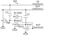
図9に示す転送回路200は、図5に示す転送回路100の出力安定化回路140に出力信号OUTを入力とした反転回路250、反転回路250の出力端がゲートに入力され、一端が出力安定化回路部の電源に接続され、他端が出力OUTに接続されているトランジスタT8を加えて新しく出力安定化回路240を形成する構成となっている。
In the
反転回路250は、トランジスタT9、T10、T11、および容量C2から構成されており、トランジスタT9、T11のゲートは制御線RSTに接続されている。また容量C2の一端は転送回路200の出力端OUTに接続され、他端はトランジスタT10のゲートおよびT11の一端に接続されている。
The inverting
トランジスタT9、T10はそれぞれ電源Vdd2とVss3間に直列に接続されており、T9とT10の接続点が反転回路の出力として前述のトランジスタT8のゲートに接続されている。トランジスタT11は一端が電源Vss4に、他端がT10と容量C2の接続点に接続される構成となっている。 The transistors T9 and T10 are connected in series between the power supplies Vdd2 and Vss3, respectively, and the connection points of T9 and T10 are connected to the gate of the above-mentioned transistor T8 as the output of the inverting circuit. One end of the transistor T11 is connected to the power supply Vss4, and the other end is connected to the connection point between T10 and the capacitance C2.
ここで、トランジスタT8は第1のトランジスタの一例であり、トランジスタT9は第2のトランジスタの一例であり、トランジスタT10は第3のトランジスタの一例であり、トランジスタT11は第4のトランジスタの一例である。 Here, the transistor T8 is an example of the first transistor, the transistor T9 is an example of the second transistor, the transistor T10 is an example of the third transistor, and the transistor T11 is an example of the fourth transistor. ..
図10に、図9に示す転送回路200の動作タイミングの一例を示す。トランジスタT9、T11のゲートに入力される制御信号RSTは、転送回路200の出力端OUTがHighレベルのときにLowレベル(図9ではVss5)であることを特徴としている。
FIG. 10 shows an example of the operation timing of the
なお、上記電圧設定およびタイミング設定は一例であり、例えばトランジスタT9が接続されている電源Vdd2がVddであっても動作上問題はない。 The voltage setting and timing setting are examples. For example, even if the power supply Vdd2 to which the transistor T9 is connected is Vdd, there is no problem in operation.
図11A〜図11Dに、転送回路200の変形例を示す。
11A to 11D show a modified example of the
図11Aに示す転送回路201は、出力安定化回路241の反転回路251に容量C3、C4を追加した構成となっている。追加した容量C3、C4の接続点の電位が安定するため、ノイズ等の影響を受けにくい構成となる。
The
図11Bに示す転送回路202は、出力安定化回路242において、トランジスタT2、T6を削除した構成となっている。後述するように、反転回路250は出力端OUTがLowレベルにあるときにトランジスタT8によって出力端OUTをVss1に接地する構成となっており、トランジスタT2およびT6はそれぞれ制御信号CLR、制御信号WRによって出力OUTをVss1に接地する構成となっているため、トランジスタT2およびT6を削除しても動作上問題とはならない。
The
図11Cに示す転送回路203は、反転回路253に入力される制御信号RSTに、転送回路203に入力される制御信号WRを使用している。前述の通り制御信号RSTは転送回路の出力端OUTがHighレベルのときにLowレベルであることを特徴としているため、制御信号WRを制御信号RSTに使用しても問題なく動作させることが可能となる。図11Cでは制御信号RSTに制御信号WRを使用しているが、制御信号CLRを使用してもよいし、図11Dに示すように、制御信号WR、制御信号CLRを並列に用いる構造としてもよい。
The
次に、転送回路200〜204の要部の動作の一例を、図12A〜図12Dの回路図を参照して説明する。なお、図12A〜図12Dに示される回路は、図11Bに示す転送回路201における出力安定化回路242の変形例であり、トランジスタT8のゲートと固定電源間に容量C3が接続された構成となっている。以降、転送回路の動作自体は前述しているため説明を省略し、反転回路とトランジスタT8について動作説明を行う。
Next, an example of the operation of the main parts of the
まず、図10の期間P2において、入力信号INがLowレベルからHighレベルに変化しており、トランジスタT1のゲート電位は上昇している。このとき制御信号RSTはHighレベルにあるため、図12Aに示すように、トランジスタT9、T11はオン状態になる。T11がオン状態になることで、トランジスタT10のゲートには電源電位Vss4が入力される。ここで、トランジスタT10のゲート−ソース間電圧がトランジスタT10の閾値電圧よりも小さくなるように電源電位Vss3、Vss4を設定することでトランジスタT10はオフ状態になる。さらに、トランジスタT9がオン状態になることでトランジスタT8のゲートには電源電位Vdd2が入力される。 First, during the period P2 of FIG. 10, the input signal IN changes from the Low level to the High level, and the gate potential of the transistor T1 rises. At this time, since the control signal RST is at the High level, the transistors T9 and T11 are turned on as shown in FIG. 12A. When T11 is turned on, the power supply potential Vss4 is input to the gate of the transistor T10. Here, the transistor T10 is turned off by setting the power supply potentials Vss3 and Vss4 so that the gate-source voltage of the transistor T10 becomes smaller than the threshold voltage of the transistor T10. Further, when the transistor T9 is turned on, the power supply potential Vdd2 is input to the gate of the transistor T8.
電源電位Vdd2が、制御信号RSTのHighレベルの電位とトランジスタT9の閾値電圧との和以下であれば、トランジスタT8のゲートには電源電位Vdd2が入力され、当該和以上であれば、電源電位Vdd2−Vth9(Vth9はトランジスタT9の閾値電圧)なる電位がトランジスタT8のゲートに入力される。いずれの場合もトランジスタT8はオン状態となるため、出力端OUTはトランジスタT8を介して電源電位Vss1に接地されることとなる。 If the power supply potential Vdd2 is equal to or less than the sum of the high level potential of the control signal RST and the threshold voltage of the transistor T9, the power supply potential Vdd2 is input to the gate of the transistor T8, and if it is equal to or more than the sum, the power supply potential Vdd2 A potential of −Vth9 (Vth9 is the threshold voltage of the transistor T9) is input to the gate of the transistor T8. In either case, since the transistor T8 is in the ON state, the output terminal OUT is grounded to the power supply potential Vss1 via the transistor T8.
図10の期間P3において、制御信号RSTがLowレベルとなる。このとき、トランジスタT9、T11はオフ状態となるが、図12Bに示すように、出力安定化回路部の各ノードの電位は保持されることとなり、出力OUTはVss1に接地される。 During the period P3 of FIG. 10, the control signal RST becomes the Low level. At this time, the transistors T9 and T11 are turned off, but as shown in FIG. 12B, the potential of each node of the output stabilization circuit unit is maintained, and the output OUT is grounded to Vss1.
その後、図12Cに示すように、出力端OUTがHighを出力する(図10の期間P3)。このとき、出力端OUTの電位は電源電位Vss1から徐々に増加する。この電位の変化が容量C2を介してトランジスタT10のゲートに入力される。トランジスタT10のゲート−ソース間電圧VgsがT10の閾値電圧よりも大きくなったとき、図12Cに示すようにトランジスタT10はオン状態となる。このときトランジスタT8のゲートには電源電位Vss3が入力され、トランジスタT8はオフし、出力端OUTの電位は電源電位Vddまで上昇する。 After that, as shown in FIG. 12C, the output end OUT outputs High (period P3 in FIG. 10). At this time, the potential of the output terminal OUT gradually increases from the power supply potential Vss1. This change in potential is input to the gate of the transistor T10 via the capacitance C2. When the gate-source voltage Vgs of the transistor T10 becomes larger than the threshold voltage of T10, the transistor T10 is turned on as shown in FIG. 12C. At this time, the power supply potential Vss3 is input to the gate of the transistor T8, the transistor T8 is turned off, and the potential of the output terminal OUT rises to the power supply potential Vdd.
一定時間経過後、制御信号ENがLowレベルに変化し、出力信号OUTもLowレベル(Vss1)に変化する。この電位の変化は図12C同様、容量C2を介してトランジスタT10のゲートに入力され、図12Dに示すように、トランジスタT10は再びオフ状態となる。 After a lapse of a certain period of time, the control signal EN changes to the Low level, and the output signal OUT also changes to the Low level (Vss1). This change in potential is input to the gate of the transistor T10 via the capacitance C2 as in FIG. 12C, and as shown in FIG. 12D, the transistor T10 is turned off again.
そして、再び制御信号RSTがHigh状態へ変化し(図10の期間P4)、図12Aに示すように、出力端OUTはトランジスタT8を介して電源電位Vss1に接地されることとなる。 Then, the control signal RST changes to the High state again (period P4 in FIG. 10), and as shown in FIG. 12A, the output terminal OUT is grounded to the power supply potential Vss1 via the transistor T8.
本発明の回路においても制御信号ENがHighレベルのとき、トランジスタT1のリーク等によって出力端OUTの電位が増加する可能性があるが、トランジスタT10がオン状態にならない限り出力端OUTはトランジスタT8を介して接地されているため、出力端OUTの電圧上昇はあったとしても小さく抑えることが可能である。 Also in the circuit of the present invention, when the control signal EN is at the high level, the potential of the output terminal OUT may increase due to leakage of the transistor T1, but the output terminal OUT uses the transistor T8 unless the transistor T10 is turned on. Since it is grounded via the above, it is possible to suppress the voltage rise of the output terminal OUT even if it is small.
また同様に、転送回路を構成するトランジスタの閾値電圧が負であり、図8Bに示すように制御信号ENがHighレベルに変化した際に出力端OUTの電位が電源電位Vss1から上昇してしまったとしても、トランジスタT10がオン状態とならない限り出力端OUTはT8を介して接地されているため、出力端OUTの電圧増加はあったとしても小さく抑えることが可能である。 Similarly, the threshold voltage of the transistors constituting the transfer circuit is negative, and the potential of the output terminal OUT rises from the power supply potential Vss1 when the control signal EN changes to the High level as shown in FIG. 8B. Even so, since the output terminal OUT is grounded via the T8 unless the transistor T10 is turned on, the voltage increase at the output terminal OUT can be suppressed to a small value even if there is an increase.
その結果、不必要なパルスの転送を防ぐことが可能となっている。 As a result, it is possible to prevent unnecessary pulse transfer.
(実施の形態2)
以下、本発明の実施の形態2について、図面を参照しながら説明する。
(Embodiment 2)
Hereinafter,
実施の形態2に係る転送回路の要部である出力安定化回路を図13A、図14Aに示す。なお、図13A、図14Aに示す出力安定化回路301、302は、図11Bに示す転送回路201における出力安定化回路242の変形例であり、T8のゲートと固定電源間に容量C3が接続された構成となっている。
The output stabilization circuit, which is a main part of the transfer circuit according to the second embodiment, is shown in FIGS. 13A and 14A. The
図13Aの出力安定化回路301では、容量C2は転送回路の出力端OUTではなく、入力端INに接続されている。出力安定化回路301は、例えば、図13Bに示す制御信号および入力信号に応じて駆動される。図13Cに、出力安定化回路301の動作波形の一例を示す。制御信号RSTは、入力端INの電位および出力端OUTの電位がHighレベルのときにLowレベルであることを特徴としている。
In the
この構成は、第2のトランジスタ(トランジスタT9)の制御信号端(ゲート)および第4のトランジスタ(トランジスタT11)の制御信号端(ゲート)に入力される制御信号(制御信号RST)は、転送回路の出力端OUTおよび入力端INが高電位側にあるとき(書込み期間および出力期間)に低電位であり、転送回路の出力端OUTおよび入力端INが低電位側にあるとき(クリア期間)に少なくとも1回は高電位となる構成の一例である。 In this configuration, the control signal (control signal RST) input to the control signal end (gate) of the second transistor (transistor T9) and the control signal end (gate) of the fourth transistor (transistor T11) is a transfer circuit. When the output end OUT and input end IN of the transfer circuit are on the high potential side (write period and output period), the potential is low, and when the output end OUT and input end IN of the transfer circuit are on the low potential side (clear period). This is an example of a configuration in which the potential is high at least once.
図14Aの出力安定化回路302では、容量C2は転送回路の出力端OUTに接続されているが、容量C3の一端が固定電源ではなく入力端INに接続されている。出力安定化回路302は、例えば、図14Bに示す制御信号および入力信号に応じて駆動される。図14Cに、出力安定化回路302の動作波形の一例を示す。制御信号RSTは、転送回路の出力端OUTの電位がHighレベルのときにLowレベルであり、入力端INの電位がHighレベルのときにHighレベルからLowレベルに変化することを特徴としている。
In the
この構成は、第2のトランジスタ(トランジスタT9)の制御信号端(ゲート)および第4のトランジスタ(トランジスタT11)の制御信号端(ゲート)に入力される制御信号(制御信号RST)は、転送回路の出力端が高電位側にあるとき(出力期間)に低電位であり、転送回路の入力端INが高電位側にあるとき(書込み期間の途中)に高電位から低電位に変化し、転送回路の出力が低電位側にあるとき(クリア期間)に少なくとも1回は高電位となる構成の一例である。 In this configuration, the control signal (control signal RST) input to the control signal end (gate) of the second transistor (transistor T9) and the control signal end (gate) of the fourth transistor (transistor T11) is a transfer circuit. When the output end of is on the high potential side (output period), it is low potential, and when the input end IN of the transfer circuit is on the high potential side (in the middle of the writing period), it changes from high potential to low potential and is transferred. This is an example of a configuration in which the potential becomes high at least once when the output of the circuit is on the low potential side (clearing period).
次に、出力安定化回路301、302の効果について説明する。
Next, the effects of the
図15は、図11Bに示す転送回路201における出力安定化回路242において出力端OUTがHighレベルに変化する際の拡大図である。
FIG. 15 is an enlarged view when the output terminal OUT changes to the High level in the
図15において、波形OUT1は、トランジスタT10がオン状態になった後、トランジスタT8のゲート電位Vg8が電源電位Vss3まで急峻に低下する場合の、出力端OUTの電位を示している。出力端OUTの電位は、速やかにHighレベルの電位である電源電位Vdd1に到達する。この場合、出力信号OUTは次段の転送回路に正しく転送される。 In FIG. 15, the waveform OUT1 shows the potential of the output end OUT when the gate potential Vg8 of the transistor T8 sharply drops to the power supply potential Vss3 after the transistor T10 is turned on. The potential of the output terminal OUT quickly reaches the power supply potential Vdd1 which is the high level potential. In this case, the output signal OUT is correctly transferred to the next-stage transfer circuit.
これに対し、トランジスタT10がオン状態になった後、トランジスタT8のゲート電位Vg8が緩慢に低下する場合について考える。トランジスタT8のゲート電位の低下が緩慢な場合、トランジスタT1、T8が共にオン状態となる期間が発生し、転送回路にはトランジスタT1、T8を介して貫通電流が流れる。これにより、出力端OUTの電位は、波形OUT2で示されるように緩やかに上昇する。 On the other hand, consider the case where the gate potential Vg8 of the transistor T8 slowly decreases after the transistor T10 is turned on. When the gate potential of the transistor T8 gradually decreases, a period in which both the transistors T1 and T8 are turned on occurs, and a through current flows through the transfer circuit through the transistors T1 and T8. As a result, the potential of the output end OUT gradually rises as shown by the waveform OUT2.
出力端OUTが、Highレベルの電位である電源電位Vdd1に到達する前に、制御信号ENがHighレベルからLowレベルに変化してしまうと、出力端OUTの電位は電源電位Vss1に低下し、出力信号OUTは十分な振幅が得られないまま次段に入力され、正常に転送が行えなくなってしまう。 If the control signal EN changes from the High level to the Low level before the output end OUT reaches the power supply potential Vdd1 which is the high level potential, the potential of the output end OUT drops to the power supply potential Vss1 and is output. The signal OUT is input to the next stage without obtaining sufficient amplitude, and normal transfer cannot be performed.
この対策として、図13Aの出力安定化回路301では、容量C2が、出力端OUTではなく、入力端INに接続されている。また、図13Bに示されるように、制御信号RSTは、転送回路の入力端INの電位および出力端OUTの電位がHighレベルのとき(例えば、書込み期間および出力期間)にLowレベルとなるように設定されている。
As a countermeasure, in the
このような構成とすることで、入力端INの電位がLowレベルからHighへと変化する電圧変化によってトランジスタT10がオン状態になった後、トランジスタT8のゲート電位Vg8が緩やかに低下したとしても転送回路に貫通電流が流れることはない。また、トランジスタT8のゲート電位Vg8が下降してから転送回路の出力端OUTの電位がLowレベルからHighレベルに変化するまで一定の時間があるため、出力端OUTの電位がLowレベルからHighレベルに変化する際、トランジスタT8のゲート電位を小さくすることができ、貫通電流によって出力端OUTの電位が大きく低下してしまうことはない。 With such a configuration, even if the gate potential Vg8 of the transistor T8 gradually decreases after the transistor T10 is turned on by the voltage change in which the potential of the input terminal IN changes from the Low level to High, the transfer is performed. No through current flows through the circuit. Further, since there is a certain time from when the gate potential Vg8 of the transistor T8 drops until the potential of the output terminal OUT of the transfer circuit changes from the Low level to the High level, the potential of the output terminal OUT changes from the Low level to the High level. When changing, the gate potential of the transistor T8 can be reduced, and the potential of the output end OUT does not drop significantly due to the through current.
また、図14Aの出力安定化回路302では、容量C2は転送回路の出力OUTに接続されているが、容量C3の一端が固定電源ではなく入力端INに接続されている。また、図14Bに示されるように、制御信号RSTは、転送回路の出力端OUTの電位がHighレベルのとき(例えば、出力期間)にLowレベルであり、入力端INの電位がHighレベルのとき(例えば、書込み期間の途中)にHighレベルからLowレベルに変化するように設定されている。
Further, in the
このような構成とすることで、制御信号RSTがHighレベルの状態で入力端INの電位がLowからHighに変化するため、トランジスタT9がオン状態であれば、つまり、電源電位Vddから電源電位Vdd2を減じた電圧値がトランジスタT9の閾値電圧よりも大きくなるように設定しておけば、トランジスタT8のゲート電位は電源電位Vdd2に接地された状態となる。その後、入力信号INがHighレベルのときに制御信号RSTをHighレベルからLowレベルに変化させてトランジスタT9をオフ状態にした後、入力信号INをHighレベルからLowレベルへと変化させる。このときトランジスタT9はオフ状態であるため、入力信号INの電位変化が容量C3を介してトランジスタT8のゲートへ入力され、トランジスタT8のゲート電位は低下する。 With such a configuration, the potential of the input terminal IN changes from Low to High when the control signal RST is at the High level. Therefore, if the transistor T9 is in the ON state, that is, the power potential Vdd to the power potential Vdd2 If the voltage value obtained by subtracting the above is set to be larger than the threshold voltage of the transistor T9, the gate potential of the transistor T8 is in a state of being grounded to the power supply potential Vdd2. After that, when the input signal IN is at the High level, the control signal RST is changed from the High level to the Low level to turn off the transistor T9, and then the input signal IN is changed from the High level to the Low level. At this time, since the transistor T9 is in the off state, the potential change of the input signal IN is input to the gate of the transistor T8 via the capacitance C3, and the gate potential of the transistor T8 decreases.
そして一定時間経過後、出力信号OUTがLowレベルからHighレベルに変化する。この電位変化によってトランジスタT10がオン状態になり、トランジスタT8のゲート電位は低下する。このとき、図15と比較してトランジスタT8のゲート電位をより小さくすることができるため、貫通電流によって出力端OUTの電位が大きく低下することを防ぐことが可能となる。 Then, after a certain period of time has elapsed, the output signal OUT changes from the Low level to the High level. Due to this potential change, the transistor T10 is turned on, and the gate potential of the transistor T8 is lowered. At this time, since the gate potential of the transistor T8 can be made smaller than that in FIG. 15, it is possible to prevent the potential of the output end OUT from being significantly lowered due to the through current.
以上説明したように、出力安定化回路301、302によれば転送回路の出力端OUTを接地することができ、トランジスタのリーク電流やバッファ回路および次段の転送回路からのリークによって出力端OUTの電位が大きく変化することを抑制できる。これにより、不必要なパルスが転送される誤転送を対策することができる。
As described above, according to the
また、転送回路の出力端OUTの電位がLowレベルからHighレベルへ遷移する際の貫通電流による出力端OUTの電位低下に起因する転送不良を対策することができる。 Further, it is possible to take measures against a transfer failure caused by a decrease in the potential of the output end OUT due to a through current when the potential of the output end OUT of the transfer circuit transitions from the Low level to the High level.
以上、本発明に係る転送回路および複数の転送回路を連ねて構成されるシフトレジスタについて実施の形態に基づいて説明したが、本発明は、この実施の形態に限定されるものではない。本発明の主旨を逸脱しない範囲で、当業者が思いつく各種変形を施し、また実施の形態における構成要素および動作を任意に組み合わせて実現される表示装置およびその駆動方法も本発明に含まれる。 The transfer circuit according to the present invention and the shift register configured by connecting a plurality of transfer circuits have been described above based on the embodiment, but the present invention is not limited to this embodiment. The present invention also includes a display device and a driving method thereof, which are realized by making various modifications that can be conceived by those skilled in the art and by arbitrarily combining the components and operations in the embodiments without departing from the gist of the present invention.
例えば、本発明のシフトレジスタと、当該シフトレジスタの各段の出力信号を処理するバッファ回路と、を備えるゲートドライバは、本発明に含まれてもよい。 For example, a gate driver including a shift register of the present invention and a buffer circuit for processing an output signal of each stage of the shift register may be included in the present invention.
また、例えば、本発明のゲートドライバを搭載した表示パネルは、本発明に含まれてもよく、また本発明のゲートドライバを搭載したフレキシブル基板は、本発明に含まれてもよい。 Further, for example, a display panel equipped with the gate driver of the present invention may be included in the present invention, and a flexible substrate equipped with the gate driver of the present invention may be included in the present invention.
本発明は、転送回路および複数の転送回路を連ねてなるシフトレジスタとして、例えば、表示装置における走査回路に利用できる。 The present invention can be used as a shift register in which a transfer circuit and a plurality of transfer circuits are connected, for example, in a scanning circuit in a display device.
10 画素回路
20 スキャナ回路
21 ライトスキャナ
22 行電源スキャナ
23 水平セレクタ
31、32 走査信号線
33 データ信号線
100、200、201、202、203、204 転送回路
110 入力回路
120 リセット回路
130 出力回路
140 出力安定化回路
141 反転回路
240〜242、301、302 出力安定化回路
250、251、253 反転回路
700 シフトレジスタ
800 バッファ回路
900 出力信号線
10
Claims (15)
前記出力安定化回路は、
前記転送回路の前記入力端および前記出力端のうちのいずれか一方または両方に接続され、前記入力信号および前記出力信号の少なくとも一方の極性を反転した反転信号を出力端から出力する反転回路と、
前記反転回路の前記出力端が制御信号端に接続され、第1の主信号端が前記出力安定化回路の電源である第1の電源に接続され、第2の主信号端が前記転送回路の前記出力端に接続されている第1のトランジスタと、を含み、
前記反転回路は、
第1の主信号端が第2の電源に接続され、第2の主信号端が前記反転回路の前記出力端に接続されている第2のトランジスタと、
第1の主信号端が前記反転回路の前記出力端に接続され、第2の主信号端が第3の電源に接続されている第3のトランジスタと、
第1の主信号端が前記第3のトランジスタの制御信号端に接続され、第2の主信号端が第4の電源に接続されている第4のトランジスタと、
一端が前記第3のトランジスタの前記制御信号端に接続され、他端が前記転送回路の前記出力端に接続されている第1の容量から形成される、
転送回路。 It consists of an input circuit, a reset circuit, an output circuit, and an output stabilization circuit. In synchronization with the clock signal, the input signal is acquired and held at the input end, and the held input signal is output from the output end as an output signal. In the transfer circuit to
The output stabilization circuit
An inverting circuit that is connected to one or both of the input terminal and the output end of the transfer circuit and outputs an inverting signal from the output terminal in which the polarity of at least one of the input signal and the output signal is inverted.
The output end of the inverting circuit is connected to the control signal end, the first main signal end is connected to the first power source which is the power source of the output stabilization circuit, and the second main signal end is the transfer circuit. Includes a first transistor connected to the output end
The inverting circuit
A second transistor having a first main signal end connected to a second power source and a second main signal end connected to the output end of the inverting circuit.
A third transistor having a first main signal end connected to the output end of the inverting circuit and a second main signal end connected to a third power source.
A fourth transistor in which the first main signal end is connected to the control signal end of the third transistor and the second main signal end is connected to the fourth power supply.
One end is connected to the control signal end of the third transistor and the other end is formed from a first capacitance connected to the output end of the transfer circuit .
Transfer circuit.
前記出力安定化回路は、
前記転送回路の前記入力端および前記出力端のうちのいずれか一方または両方に接続され、前記入力信号および前記出力信号の少なくとも一方の極性を反転した反転信号を出力端から出力する反転回路と、
前記反転回路の前記出力端が制御信号端に接続され、第1の主信号端が前記出力安定化回路の電源である第1の電源に接続され、第2の主信号端が前記転送回路の前記出力端に接続されている第1のトランジスタと、を含み、
前記反転回路は、
第1の主信号端が第2の電源に接続され、第2の主信号端が前記反転回路の前記出力端に接続されている第2のトランジスタと、
第1の主信号端が前記反転回路の前記出力端に接続され、第2の主信号端が第3の電源に接続されている第3のトランジスタと、
第1の主信号端が前記第3のトランジスタの制御信号端に接続され、第2の主信号端が第4の電源に接続されている第4のトランジスタと、
一端が前記第3のトランジスタの前記制御信号端に接続され、他端が前記転送回路の前記入力端に接続されている第1の容量から形成される、
転送回路。 It consists of an input circuit, a reset circuit, an output circuit, and an output stabilization circuit. In synchronization with the clock signal, the input signal is acquired and held at the input end, and the held input signal is output from the output end as an output signal. In the transfer circuit to
The output stabilization circuit
An inverting circuit that is connected to one or both of the input terminal and the output end of the transfer circuit and outputs an inverting signal from the output terminal in which the polarity of at least one of the input signal and the output signal is inverted.
The output end of the inverting circuit is connected to the control signal end, the first main signal end is connected to the first power source which is the power source of the output stabilization circuit, and the second main signal end is the transfer circuit. Includes a first transistor connected to the output end
The inverting circuit
A second transistor having a first main signal end connected to a second power source and a second main signal end connected to the output end of the inverting circuit.
A third transistor having a first main signal end connected to the output end of the inverting circuit and a second main signal end connected to a third power source.
A fourth transistor having a first main signal end connected to the control signal end of the third transistor and a second main signal end connected to a fourth power source.
One end is connected to the control signal end of the third transistor and the other end is formed from a first capacitance connected to the input end of the transfer circuit .
Transfer circuit.
前記出力安定化回路は、
前記転送回路の前記入力端および前記出力端のうちのいずれか一方または両方に接続され、前記入力信号および前記出力信号の少なくとも一方の極性を反転した反転信号を出力端から出力する反転回路と、
前記反転回路の前記出力端が制御信号端に接続され、第1の主信号端が前記出力安定化回路の電源である第1の電源に接続され、第2の主信号端が前記転送回路の前記出力端に接続されている第1のトランジスタと、を含み、
前記反転回路は、
第1の主信号端が第2の電源に接続され、第2の主信号端が前記反転回路の前記出力端に接続されている第2のトランジスタと、
第1の主信号端が前記反転回路の前記出力端に接続され、第2の主信号端が第3の電源に接続されている第3のトランジスタと、
第1の主信号端が前記第3のトランジスタの制御信号端に接続され、第2の主信号端が第4の電源に接続されている第4のトランジスタと、
一端が前記第3のトランジスタの制御信号端に接続され、他端が前記転送回路の前記出力端に接続されている第1の容量と、
一端が前記転送回路の前記入力端に接続され、他端が前記反転回路の前記出力端に接続された第2の容量から形成される、
転送回路。 It consists of an input circuit, a reset circuit, an output circuit, and an output stabilization circuit. In synchronization with the clock signal, the input signal is acquired and held at the input end, and the held input signal is output from the output end as an output signal. In the transfer circuit to
The output stabilization circuit
An inverting circuit that is connected to one or both of the input terminal and the output end of the transfer circuit and outputs an inverting signal from the output terminal in which the polarity of at least one of the input signal and the output signal is inverted.
The output end of the inverting circuit is connected to the control signal end, the first main signal end is connected to the first power source which is the power source of the output stabilization circuit, and the second main signal end is the transfer circuit. Includes a first transistor connected to the output end
The inverting circuit
A second transistor having a first main signal end connected to a second power source and a second main signal end connected to the output end of the inverting circuit.
A third transistor having a first main signal end connected to the output end of the inverting circuit and a second main signal end connected to a third power source.
A fourth transistor having a first main signal end connected to the control signal end of the third transistor and a second main signal end connected to a fourth power source.
A first capacitance having one end connected to the control signal end of the third transistor and the other end connected to the output end of the transfer circuit.
One end is connected to the input end of the transfer circuit and the other end is formed from a second capacitance connected to the output end of the inverting circuit .
Transfer circuit.
第3の電源の電位は前記低電位側の電位以下であり、かつ前記第4の電源の電位は前記第3の電源の電位以下である、
請求項1から3のいずれか1項に記載の転送回路。 The potential of the second power supply is higher than the potential on the low potential side output from the transfer circuit, the potential of the third power supply is equal to or lower than the potential on the low potential side, and the potential of the fourth power supply is Is equal to or lower than the potential of the third power source.
The transfer circuit according to any one of claims 1 to 3 .
請求項1から3のいずれか1項に記載の転送回路。 A capacitance is formed between the output end of the inverting circuit and the fixed power supply.
The transfer circuit according to any one of claims 1 to 3 .
請求項1から3のいずれか1項に記載の転送回路。 A capacitance is formed between the control signal terminal of the third transistor and the fixed power supply.
The transfer circuit according to any one of claims 1 to 3 .
請求項1に記載の転送回路。 The control signal input to the control signal end of the second transistor and the control signal end of the fourth transistor has a low potential when the output of the transfer circuit is on the high potential side, and is the output of the transfer circuit. At least once when is on the low potential side,
The transfer circuit according to claim 1 .
請求項2に記載の転送回路。 The control signal input to the control signal end of the second transistor and the control signal end of the fourth transistor has a low potential when the output and input of the transfer circuit are on the high potential side, and the transfer circuit High potential at least once when the output and input of is on the low potential side,
The transfer circuit according to claim 2 .
請求項3に記載の転送回路。 The control signal input to the control signal end of the second transistor and the control signal end of the fourth transistor has a low potential when the output of the transfer circuit is on the high potential side, and is an input of the transfer circuit. Changes from high potential to low potential when is on the high potential side, and becomes high potential at least once when the output of the transfer circuit is on the low potential side.
The transfer circuit according to claim 3 .
請求項7から9のいずれか1項に記載の転送回路。 The control signal input to the control signal end of the second transistor and the control signal end of the fourth transistor are the same signal.
The transfer circuit according to any one of claims 7 to 9 .
請求項10に記載の転送回路。 The same signal input to the control signal end of the second transistor and the control signal end of the fourth transistor is controlled to be input to at least one of the input circuit and the reset circuit of the transfer circuit. Same as the signal,
The transfer circuit according to claim 10 .
前記シフトレジスタの各段の出力信号を処理するバッファ回路と、
を備えるゲートドライバ。 The shift register according to claim 12 and
A buffer circuit that processes the output signal of each stage of the shift register and
A gate driver equipped with.
Priority Applications (3)
| Application Number | Priority Date | Filing Date | Title |
|---|---|---|---|
| JP2018001893A JP6754786B2 (en) | 2018-01-10 | 2018-01-10 | Transfer circuits, shift registers, gate drivers, display panels, and flexible boards |
| CN201811568870.3A CN110021332A (en) | 2018-01-10 | 2018-12-21 | Transmission circuit, shift register, gate drivers, display panel and flexible base board |
| US16/233,956 US10783822B2 (en) | 2018-01-10 | 2018-12-27 | Transfer circuit, shift register, gate driver, display panel, and flexible substrate |
Applications Claiming Priority (1)
| Application Number | Priority Date | Filing Date | Title |
|---|---|---|---|
| JP2018001893A JP6754786B2 (en) | 2018-01-10 | 2018-01-10 | Transfer circuits, shift registers, gate drivers, display panels, and flexible boards |
Publications (3)
| Publication Number | Publication Date |
|---|---|
| JP2019121411A JP2019121411A (en) | 2019-07-22 |
| JP2019121411A5 JP2019121411A5 (en) | 2019-09-05 |
| JP6754786B2 true JP6754786B2 (en) | 2020-09-16 |
Family
ID=67140231
Family Applications (1)
| Application Number | Title | Priority Date | Filing Date |
|---|---|---|---|
| JP2018001893A Active JP6754786B2 (en) | 2018-01-10 | 2018-01-10 | Transfer circuits, shift registers, gate drivers, display panels, and flexible boards |
Country Status (3)
| Country | Link |
|---|---|
| US (1) | US10783822B2 (en) |
| JP (1) | JP6754786B2 (en) |
| CN (1) | CN110021332A (en) |
Families Citing this family (2)
| Publication number | Priority date | Publication date | Assignee | Title |
|---|---|---|---|---|
| JP6874997B2 (en) * | 2018-01-16 | 2021-05-19 | 株式会社Joled | Transfer circuits, shift registers, gate drivers, display panels, and flexible boards |
| WO2021184260A1 (en) * | 2020-03-18 | 2021-09-23 | 京东方科技集团股份有限公司 | Shift register unit and driving method therefor, and gate driving circuit and display apparatus |
Family Cites Families (8)
| Publication number | Priority date | Publication date | Assignee | Title |
|---|---|---|---|---|
| US8605027B2 (en) * | 2004-06-30 | 2013-12-10 | Samsung Display Co., Ltd. | Shift register, display device having the same and method of driving the same |
| JP5659906B2 (en) * | 2010-03-30 | 2015-01-28 | ソニー株式会社 | Inverter circuit and display device |
| US8803785B2 (en) | 2010-04-12 | 2014-08-12 | Sharp Kabushiki Kaisha | Scanning signal line drive circuit and display device having the same |
| CN106688029A (en) * | 2014-05-28 | 2017-05-17 | 可隆奥托株式会社 | Shift circuit, shift resistor, and display device |
| JP6561381B2 (en) | 2015-08-25 | 2019-08-21 | 株式会社Joled | Register circuit, drive circuit, and display device |
| US10431159B2 (en) | 2015-08-25 | 2019-10-01 | Joled Inc. | Register circuit, driver circuit, and display unit |
| CN105489189B (en) * | 2016-02-01 | 2018-09-18 | 京东方科技集团股份有限公司 | Drive element of the grid, gate driving circuit and its driving method and display device |
| CN105810167B (en) * | 2016-05-23 | 2019-06-04 | 信利(惠州)智能显示有限公司 | Shift register cell circuit, shift register and its liquid crystal display |
-
2018
- 2018-01-10 JP JP2018001893A patent/JP6754786B2/en active Active
- 2018-12-21 CN CN201811568870.3A patent/CN110021332A/en active Pending
- 2018-12-27 US US16/233,956 patent/US10783822B2/en active Active
Also Published As
| Publication number | Publication date |
|---|---|
| US10783822B2 (en) | 2020-09-22 |
| US20190213945A1 (en) | 2019-07-11 |
| CN110021332A (en) | 2019-07-16 |
| JP2019121411A (en) | 2019-07-22 |
Similar Documents
| Publication | Publication Date | Title |
|---|---|---|
| US8018423B2 (en) | Shift register and liquid crystal display | |
| US7664218B2 (en) | Shift register and image display apparatus containing the same | |
| EP3832635A1 (en) | Shift register, gate driving circuit, display device, and gate driving method | |
| JP5078533B2 (en) | Gate line drive circuit | |
| US8223110B2 (en) | Displays | |
| US9905311B2 (en) | Shift register circuit, drive circuit, and display device | |
| CN107895562B (en) | High-stability pulse width adjustable shift register | |
| WO2010050262A1 (en) | Shift register circuit, display device and shift register circuit driving method | |
| US20150138176A1 (en) | Scanning signal line drive circuit and display device provided with same | |
| US20110001689A1 (en) | Active matrix type display apparatus | |
| US7787585B2 (en) | Shift registers | |
| CN109656397B (en) | Touch control display device | |
| US10923064B2 (en) | Scanning signal line drive circuit and display device equipped with same | |
| CN112802422A (en) | Shift register, grid drive circuit and display panel | |
| JP6754786B2 (en) | Transfer circuits, shift registers, gate drivers, display panels, and flexible boards | |
| US10529296B2 (en) | Scanning line drive circuit and display device including the same | |
| JP2009181612A (en) | Shift register circuit and liquid crystal display unit | |
| JP6110177B2 (en) | Shift register circuit and image display device | |
| JP6874997B2 (en) | Transfer circuits, shift registers, gate drivers, display panels, and flexible boards | |
| CN108305584B (en) | Driving circuit | |
| KR101502174B1 (en) | Gate driver and display device | |
| JP2006203503A (en) | Level shifter, drive method thereof, electro-optical device, drive method thereof, and electronic apparatus | |
| JP2017227820A (en) | Display | |
| US11200862B2 (en) | Shift register and display device provided with the same | |
| JP2007057637A (en) | Driving device and driving method for display panel |
Legal Events
| Date | Code | Title | Description |
|---|---|---|---|
| A521 | Request for written amendment filed |
Free format text: JAPANESE INTERMEDIATE CODE: A523 Effective date: 20190726 |
|
| A621 | Written request for application examination |
Free format text: JAPANESE INTERMEDIATE CODE: A621 Effective date: 20190726 |
|
| A977 | Report on retrieval |
Free format text: JAPANESE INTERMEDIATE CODE: A971007 Effective date: 20200514 |
|
| A131 | Notification of reasons for refusal |
Free format text: JAPANESE INTERMEDIATE CODE: A131 Effective date: 20200526 |
|
| A521 | Request for written amendment filed |
Free format text: JAPANESE INTERMEDIATE CODE: A523 Effective date: 20200713 |
|
| TRDD | Decision of grant or rejection written | ||
| A01 | Written decision to grant a patent or to grant a registration (utility model) |
Free format text: JAPANESE INTERMEDIATE CODE: A01 Effective date: 20200804 |
|
| A61 | First payment of annual fees (during grant procedure) |
Free format text: JAPANESE INTERMEDIATE CODE: A61 Effective date: 20200824 |
|
| R151 | Written notification of patent or utility model registration |
Ref document number: 6754786 Country of ref document: JP Free format text: JAPANESE INTERMEDIATE CODE: R151 |
|
| S303 | Written request for registration of pledge or change of pledge |
Free format text: JAPANESE INTERMEDIATE CODE: R316303 |
|
| R350 | Written notification of registration of transfer |
Free format text: JAPANESE INTERMEDIATE CODE: R350 |
|
| S803 | Written request for registration of cancellation of provisional registration |
Free format text: JAPANESE INTERMEDIATE CODE: R316803 |
|
| R350 | Written notification of registration of transfer |
Free format text: JAPANESE INTERMEDIATE CODE: R350 |
|
| R250 | Receipt of annual fees |
Free format text: JAPANESE INTERMEDIATE CODE: R250 |