JP6736531B2 - Semiconductor device - Google Patents
Semiconductor device Download PDFInfo
- Publication number
- JP6736531B2 JP6736531B2 JP2017176263A JP2017176263A JP6736531B2 JP 6736531 B2 JP6736531 B2 JP 6736531B2 JP 2017176263 A JP2017176263 A JP 2017176263A JP 2017176263 A JP2017176263 A JP 2017176263A JP 6736531 B2 JP6736531 B2 JP 6736531B2
- Authority
- JP
- Japan
- Prior art keywords
- region
- trench
- igbt
- type
- diode
- Prior art date
- Legal status (The legal status is an assumption and is not a legal conclusion. Google has not performed a legal analysis and makes no representation as to the accuracy of the status listed.)
- Active
Links
- 239000004065 semiconductor Substances 0.000 title claims description 99
- 239000012535 impurity Substances 0.000 claims description 33
- 230000000052 comparative effect Effects 0.000 description 12
- ZOXJGFHDIHLPTG-UHFFFAOYSA-N Boron Chemical compound [B] ZOXJGFHDIHLPTG-UHFFFAOYSA-N 0.000 description 5
- 229910052796 boron Inorganic materials 0.000 description 5
- OAICVXFJPJFONN-UHFFFAOYSA-N Phosphorus Chemical compound [P] OAICVXFJPJFONN-UHFFFAOYSA-N 0.000 description 4
- 229910052698 phosphorus Inorganic materials 0.000 description 4
- 239000011574 phosphorus Substances 0.000 description 4
- 239000000969 carrier Substances 0.000 description 3
- 238000010586 diagram Methods 0.000 description 3
- VYPSYNLAJGMNEJ-UHFFFAOYSA-N Silicium dioxide Chemical compound O=[Si]=O VYPSYNLAJGMNEJ-UHFFFAOYSA-N 0.000 description 2
- 229910052785 arsenic Inorganic materials 0.000 description 2
- RQNWIZPPADIBDY-UHFFFAOYSA-N arsenic atom Chemical compound [As] RQNWIZPPADIBDY-UHFFFAOYSA-N 0.000 description 2
- 230000000694 effects Effects 0.000 description 2
- 229910052751 metal Inorganic materials 0.000 description 2
- 239000002184 metal Substances 0.000 description 2
- 229910021420 polycrystalline silicon Inorganic materials 0.000 description 2
- 229910052814 silicon oxide Inorganic materials 0.000 description 2
- 238000004088 simulation Methods 0.000 description 2
- XUIMIQQOPSSXEZ-UHFFFAOYSA-N Silicon Chemical compound [Si] XUIMIQQOPSSXEZ-UHFFFAOYSA-N 0.000 description 1
- 230000015556 catabolic process Effects 0.000 description 1
- 239000012141 concentrate Substances 0.000 description 1
- 230000005684 electric field Effects 0.000 description 1
- 230000004048 modification Effects 0.000 description 1
- 238000012986 modification Methods 0.000 description 1
- 229910021421 monocrystalline silicon Inorganic materials 0.000 description 1
- 229910052710 silicon Inorganic materials 0.000 description 1
- 239000010703 silicon Substances 0.000 description 1
- 238000010408 sweeping Methods 0.000 description 1
Images


Classifications
-
- H—ELECTRICITY
- H01—ELECTRIC ELEMENTS
- H01L—SEMICONDUCTOR DEVICES NOT COVERED BY CLASS H10
- H01L27/00—Devices consisting of a plurality of semiconductor or other solid-state components formed in or on a common substrate
- H01L27/02—Devices consisting of a plurality of semiconductor or other solid-state components formed in or on a common substrate including semiconductor components specially adapted for rectifying, oscillating, amplifying or switching and having at least one potential-jump barrier or surface barrier; including integrated passive circuit elements with at least one potential-jump barrier or surface barrier
- H01L27/04—Devices consisting of a plurality of semiconductor or other solid-state components formed in or on a common substrate including semiconductor components specially adapted for rectifying, oscillating, amplifying or switching and having at least one potential-jump barrier or surface barrier; including integrated passive circuit elements with at least one potential-jump barrier or surface barrier the substrate being a semiconductor body
- H01L27/06—Devices consisting of a plurality of semiconductor or other solid-state components formed in or on a common substrate including semiconductor components specially adapted for rectifying, oscillating, amplifying or switching and having at least one potential-jump barrier or surface barrier; including integrated passive circuit elements with at least one potential-jump barrier or surface barrier the substrate being a semiconductor body including a plurality of individual components in a non-repetitive configuration
- H01L27/07—Devices consisting of a plurality of semiconductor or other solid-state components formed in or on a common substrate including semiconductor components specially adapted for rectifying, oscillating, amplifying or switching and having at least one potential-jump barrier or surface barrier; including integrated passive circuit elements with at least one potential-jump barrier or surface barrier the substrate being a semiconductor body including a plurality of individual components in a non-repetitive configuration the components having an active region in common
- H01L27/0705—Devices consisting of a plurality of semiconductor or other solid-state components formed in or on a common substrate including semiconductor components specially adapted for rectifying, oscillating, amplifying or switching and having at least one potential-jump barrier or surface barrier; including integrated passive circuit elements with at least one potential-jump barrier or surface barrier the substrate being a semiconductor body including a plurality of individual components in a non-repetitive configuration the components having an active region in common comprising components of the field effect type
- H01L27/0727—Devices consisting of a plurality of semiconductor or other solid-state components formed in or on a common substrate including semiconductor components specially adapted for rectifying, oscillating, amplifying or switching and having at least one potential-jump barrier or surface barrier; including integrated passive circuit elements with at least one potential-jump barrier or surface barrier the substrate being a semiconductor body including a plurality of individual components in a non-repetitive configuration the components having an active region in common comprising components of the field effect type in combination with diodes, or capacitors or resistors
-
- H—ELECTRICITY
- H01—ELECTRIC ELEMENTS
- H01L—SEMICONDUCTOR DEVICES NOT COVERED BY CLASS H10
- H01L27/00—Devices consisting of a plurality of semiconductor or other solid-state components formed in or on a common substrate
- H01L27/02—Devices consisting of a plurality of semiconductor or other solid-state components formed in or on a common substrate including semiconductor components specially adapted for rectifying, oscillating, amplifying or switching and having at least one potential-jump barrier or surface barrier; including integrated passive circuit elements with at least one potential-jump barrier or surface barrier
- H01L27/04—Devices consisting of a plurality of semiconductor or other solid-state components formed in or on a common substrate including semiconductor components specially adapted for rectifying, oscillating, amplifying or switching and having at least one potential-jump barrier or surface barrier; including integrated passive circuit elements with at least one potential-jump barrier or surface barrier the substrate being a semiconductor body
- H01L27/06—Devices consisting of a plurality of semiconductor or other solid-state components formed in or on a common substrate including semiconductor components specially adapted for rectifying, oscillating, amplifying or switching and having at least one potential-jump barrier or surface barrier; including integrated passive circuit elements with at least one potential-jump barrier or surface barrier the substrate being a semiconductor body including a plurality of individual components in a non-repetitive configuration
- H01L27/0611—Devices consisting of a plurality of semiconductor or other solid-state components formed in or on a common substrate including semiconductor components specially adapted for rectifying, oscillating, amplifying or switching and having at least one potential-jump barrier or surface barrier; including integrated passive circuit elements with at least one potential-jump barrier or surface barrier the substrate being a semiconductor body including a plurality of individual components in a non-repetitive configuration integrated circuits having a two-dimensional layout of components without a common active region
- H01L27/0617—Devices consisting of a plurality of semiconductor or other solid-state components formed in or on a common substrate including semiconductor components specially adapted for rectifying, oscillating, amplifying or switching and having at least one potential-jump barrier or surface barrier; including integrated passive circuit elements with at least one potential-jump barrier or surface barrier the substrate being a semiconductor body including a plurality of individual components in a non-repetitive configuration integrated circuits having a two-dimensional layout of components without a common active region comprising components of the field-effect type
- H01L27/0629—Devices consisting of a plurality of semiconductor or other solid-state components formed in or on a common substrate including semiconductor components specially adapted for rectifying, oscillating, amplifying or switching and having at least one potential-jump barrier or surface barrier; including integrated passive circuit elements with at least one potential-jump barrier or surface barrier the substrate being a semiconductor body including a plurality of individual components in a non-repetitive configuration integrated circuits having a two-dimensional layout of components without a common active region comprising components of the field-effect type in combination with diodes, or resistors, or capacitors
-
- H—ELECTRICITY
- H01—ELECTRIC ELEMENTS
- H01L—SEMICONDUCTOR DEVICES NOT COVERED BY CLASS H10
- H01L27/00—Devices consisting of a plurality of semiconductor or other solid-state components formed in or on a common substrate
- H01L27/02—Devices consisting of a plurality of semiconductor or other solid-state components formed in or on a common substrate including semiconductor components specially adapted for rectifying, oscillating, amplifying or switching and having at least one potential-jump barrier or surface barrier; including integrated passive circuit elements with at least one potential-jump barrier or surface barrier
- H01L27/04—Devices consisting of a plurality of semiconductor or other solid-state components formed in or on a common substrate including semiconductor components specially adapted for rectifying, oscillating, amplifying or switching and having at least one potential-jump barrier or surface barrier; including integrated passive circuit elements with at least one potential-jump barrier or surface barrier the substrate being a semiconductor body
- H01L27/06—Devices consisting of a plurality of semiconductor or other solid-state components formed in or on a common substrate including semiconductor components specially adapted for rectifying, oscillating, amplifying or switching and having at least one potential-jump barrier or surface barrier; including integrated passive circuit elements with at least one potential-jump barrier or surface barrier the substrate being a semiconductor body including a plurality of individual components in a non-repetitive configuration
- H01L27/0611—Devices consisting of a plurality of semiconductor or other solid-state components formed in or on a common substrate including semiconductor components specially adapted for rectifying, oscillating, amplifying or switching and having at least one potential-jump barrier or surface barrier; including integrated passive circuit elements with at least one potential-jump barrier or surface barrier the substrate being a semiconductor body including a plurality of individual components in a non-repetitive configuration integrated circuits having a two-dimensional layout of components without a common active region
- H01L27/0641—Devices consisting of a plurality of semiconductor or other solid-state components formed in or on a common substrate including semiconductor components specially adapted for rectifying, oscillating, amplifying or switching and having at least one potential-jump barrier or surface barrier; including integrated passive circuit elements with at least one potential-jump barrier or surface barrier the substrate being a semiconductor body including a plurality of individual components in a non-repetitive configuration integrated circuits having a two-dimensional layout of components without a common active region without components of the field effect type
- H01L27/0647—Bipolar transistors in combination with diodes, or capacitors, or resistors, e.g. vertical bipolar transistor and bipolar lateral transistor and resistor
- H01L27/0652—Vertical bipolar transistor in combination with diodes, or capacitors, or resistors
- H01L27/0664—Vertical bipolar transistor in combination with diodes
-
- H—ELECTRICITY
- H01—ELECTRIC ELEMENTS
- H01L—SEMICONDUCTOR DEVICES NOT COVERED BY CLASS H10
- H01L29/00—Semiconductor devices adapted for rectifying, amplifying, oscillating or switching, or capacitors or resistors with at least one potential-jump barrier or surface barrier, e.g. PN junction depletion layer or carrier concentration layer; Details of semiconductor bodies or of electrodes thereof ; Multistep manufacturing processes therefor
- H01L29/02—Semiconductor bodies ; Multistep manufacturing processes therefor
- H01L29/06—Semiconductor bodies ; Multistep manufacturing processes therefor characterised by their shape; characterised by the shapes, relative sizes, or dispositions of the semiconductor regions ; characterised by the concentration or distribution of impurities within semiconductor regions
- H01L29/0684—Semiconductor bodies ; Multistep manufacturing processes therefor characterised by their shape; characterised by the shapes, relative sizes, or dispositions of the semiconductor regions ; characterised by the concentration or distribution of impurities within semiconductor regions characterised by the shape, relative sizes or dispositions of the semiconductor regions or junctions between the regions
- H01L29/0692—Surface layout
- H01L29/0696—Surface layout of cellular field-effect devices, e.g. multicellular DMOS transistors or IGBTs
-
- H—ELECTRICITY
- H01—ELECTRIC ELEMENTS
- H01L—SEMICONDUCTOR DEVICES NOT COVERED BY CLASS H10
- H01L29/00—Semiconductor devices adapted for rectifying, amplifying, oscillating or switching, or capacitors or resistors with at least one potential-jump barrier or surface barrier, e.g. PN junction depletion layer or carrier concentration layer; Details of semiconductor bodies or of electrodes thereof ; Multistep manufacturing processes therefor
- H01L29/02—Semiconductor bodies ; Multistep manufacturing processes therefor
- H01L29/06—Semiconductor bodies ; Multistep manufacturing processes therefor characterised by their shape; characterised by the shapes, relative sizes, or dispositions of the semiconductor regions ; characterised by the concentration or distribution of impurities within semiconductor regions
- H01L29/08—Semiconductor bodies ; Multistep manufacturing processes therefor characterised by their shape; characterised by the shapes, relative sizes, or dispositions of the semiconductor regions ; characterised by the concentration or distribution of impurities within semiconductor regions with semiconductor regions connected to an electrode carrying current to be rectified, amplified or switched and such electrode being part of a semiconductor device which comprises three or more electrodes
- H01L29/083—Anode or cathode regions of thyristors or gated bipolar-mode devices
- H01L29/0834—Anode regions of thyristors or gated bipolar-mode devices, e.g. supplementary regions surrounding anode regions
-
- H—ELECTRICITY
- H01—ELECTRIC ELEMENTS
- H01L—SEMICONDUCTOR DEVICES NOT COVERED BY CLASS H10
- H01L29/00—Semiconductor devices adapted for rectifying, amplifying, oscillating or switching, or capacitors or resistors with at least one potential-jump barrier or surface barrier, e.g. PN junction depletion layer or carrier concentration layer; Details of semiconductor bodies or of electrodes thereof ; Multistep manufacturing processes therefor
- H01L29/40—Electrodes ; Multistep manufacturing processes therefor
- H01L29/402—Field plates
- H01L29/407—Recessed field plates, e.g. trench field plates, buried field plates
-
- H—ELECTRICITY
- H01—ELECTRIC ELEMENTS
- H01L—SEMICONDUCTOR DEVICES NOT COVERED BY CLASS H10
- H01L29/00—Semiconductor devices adapted for rectifying, amplifying, oscillating or switching, or capacitors or resistors with at least one potential-jump barrier or surface barrier, e.g. PN junction depletion layer or carrier concentration layer; Details of semiconductor bodies or of electrodes thereof ; Multistep manufacturing processes therefor
- H01L29/40—Electrodes ; Multistep manufacturing processes therefor
- H01L29/41—Electrodes ; Multistep manufacturing processes therefor characterised by their shape, relative sizes or dispositions
- H01L29/423—Electrodes ; Multistep manufacturing processes therefor characterised by their shape, relative sizes or dispositions not carrying the current to be rectified, amplified or switched
- H01L29/42312—Gate electrodes for field effect devices
- H01L29/42316—Gate electrodes for field effect devices for field-effect transistors
- H01L29/4232—Gate electrodes for field effect devices for field-effect transistors with insulated gate
- H01L29/42356—Disposition, e.g. buried gate electrode
- H01L29/4236—Disposition, e.g. buried gate electrode within a trench, e.g. trench gate electrode, groove gate electrode
-
- H—ELECTRICITY
- H01—ELECTRIC ELEMENTS
- H01L—SEMICONDUCTOR DEVICES NOT COVERED BY CLASS H10
- H01L29/00—Semiconductor devices adapted for rectifying, amplifying, oscillating or switching, or capacitors or resistors with at least one potential-jump barrier or surface barrier, e.g. PN junction depletion layer or carrier concentration layer; Details of semiconductor bodies or of electrodes thereof ; Multistep manufacturing processes therefor
- H01L29/66—Types of semiconductor device ; Multistep manufacturing processes therefor
- H01L29/68—Types of semiconductor device ; Multistep manufacturing processes therefor controllable by only the electric current supplied, or only the electric potential applied, to an electrode which does not carry the current to be rectified, amplified or switched
- H01L29/70—Bipolar devices
- H01L29/72—Transistor-type devices, i.e. able to continuously respond to applied control signals
- H01L29/739—Transistor-type devices, i.e. able to continuously respond to applied control signals controlled by field-effect, e.g. bipolar static induction transistors [BSIT]
- H01L29/7393—Insulated gate bipolar mode transistors, i.e. IGBT; IGT; COMFET
- H01L29/7395—Vertical transistors, e.g. vertical IGBT
- H01L29/7396—Vertical transistors, e.g. vertical IGBT with a non planar surface, e.g. with a non planar gate or with a trench or recess or pillar in the surface of the emitter, base or collector region for improving current density or short circuiting the emitter and base regions
- H01L29/7397—Vertical transistors, e.g. vertical IGBT with a non planar surface, e.g. with a non planar gate or with a trench or recess or pillar in the surface of the emitter, base or collector region for improving current density or short circuiting the emitter and base regions and a gate structure lying on a slanted or vertical surface or formed in a groove, e.g. trench gate IGBT
-
- H—ELECTRICITY
- H01—ELECTRIC ELEMENTS
- H01L—SEMICONDUCTOR DEVICES NOT COVERED BY CLASS H10
- H01L29/00—Semiconductor devices adapted for rectifying, amplifying, oscillating or switching, or capacitors or resistors with at least one potential-jump barrier or surface barrier, e.g. PN junction depletion layer or carrier concentration layer; Details of semiconductor bodies or of electrodes thereof ; Multistep manufacturing processes therefor
- H01L29/66—Types of semiconductor device ; Multistep manufacturing processes therefor
- H01L29/86—Types of semiconductor device ; Multistep manufacturing processes therefor controllable only by variation of the electric current supplied, or only the electric potential applied, to one or more of the electrodes carrying the current to be rectified, amplified, oscillated or switched
- H01L29/861—Diodes
- H01L29/8613—Mesa PN junction diodes
-
- H—ELECTRICITY
- H01—ELECTRIC ELEMENTS
- H01L—SEMICONDUCTOR DEVICES NOT COVERED BY CLASS H10
- H01L29/00—Semiconductor devices adapted for rectifying, amplifying, oscillating or switching, or capacitors or resistors with at least one potential-jump barrier or surface barrier, e.g. PN junction depletion layer or carrier concentration layer; Details of semiconductor bodies or of electrodes thereof ; Multistep manufacturing processes therefor
- H01L29/02—Semiconductor bodies ; Multistep manufacturing processes therefor
- H01L29/06—Semiconductor bodies ; Multistep manufacturing processes therefor characterised by their shape; characterised by the shapes, relative sizes, or dispositions of the semiconductor regions ; characterised by the concentration or distribution of impurities within semiconductor regions
- H01L29/0684—Semiconductor bodies ; Multistep manufacturing processes therefor characterised by their shape; characterised by the shapes, relative sizes, or dispositions of the semiconductor regions ; characterised by the concentration or distribution of impurities within semiconductor regions characterised by the shape, relative sizes or dispositions of the semiconductor regions or junctions between the regions
- H01L29/0692—Surface layout
Description
本発明の実施形態は、半導体装置に関する。 Embodiments of the present invention relate to a semiconductor device.
RC(Reverse Conducting)−IGBT(Insulated Gate Bipolar Transistor)は、IGBTが形成されたIGBT部と、IGBT部に隣接しダイオードが形成されたダイオード部とが、同一の半導体層に形成される。RC−IGBTでは、ダイオードが順方向動作する際に、隣接するIGBT部のゲート電極に電圧が印加されるとチャネルが形成されて、キャリアが排出される。このため、ダイオードの電流電圧特性にスナップバックが生じるおそれがある。ダイオード部でスナップバックが生じると、例えば、複数のRC−IGBTを並列接続している場合に、特定のRC−IGBTに電流が集中し、特定のRC−IGBTが破壊するおそれがある。 In RC (Reverse Conducting)-IGBT (Insulated Gate Bipolar Transistor), an IGBT part in which an IGBT is formed and a diode part in which a diode is formed adjacent to the IGBT part are formed in the same semiconductor layer. In the RC-IGBT, when a diode operates in the forward direction, a channel is formed when a voltage is applied to the gate electrode of the adjacent IGBT section, and carriers are discharged. Therefore, snapback may occur in the current-voltage characteristics of the diode. If snapback occurs in the diode portion, for example, when a plurality of RC-IGBTs are connected in parallel, current may concentrate in a specific RC-IGBT and the specific RC-IGBT may be destroyed.
本発明が解決しようとする課題は、ダイオードのスナップバックを抑制することが可能な半導体装置を提供することにある。 The problem to be solved by the present invention is to provide a semiconductor device capable of suppressing snapback of a diode.
一つの実施形態の半導体装置は、第1の面と第2の面を有する半導体層の中に設けられた第1導電型の第1のアノード領域と、前記第1のアノード領域と前記第2の面との間に設けられた第2導電型の第1のカソード領域と、前記第1のアノード領域と前記第1のカソード領域との間に設けられ、前記第1のカソード領域よりも第2導電型の不純物濃度の低い第2導電型のドリフト領域と、前記半導体層の中に設けられて第1の方向に伸長する第1のトレンチと、前記第1のトレンチの中に設けられた第1のトレンチ絶縁膜と、前記第1のトレンチの中であって前記第1のトレンチ絶縁膜の上に設けられ、前記第1のアノード領域に電気的に接続された第1のトレンチ電極と、を有する第1のダイオード部と、前記半導体層の中に設けられた第1導電型の第2のアノード領域と、前記第2のアノード領域と前記第2の面との間に設けられた第2導電型の第2のカソード領域と、前記第2のアノード領域と前記第2のカソード領域との間に設けられた前記ドリフト領域と、前記半導体層の中に設けられて前記第1の方向に伸長する第2のトレンチと、前記第2のトレンチの中に設けられた第2のトレンチ絶縁膜と、前記第2のトレンチの中であって前記第2のトレンチ絶縁膜の上に設けられ、前記第2のアノード領域に電気的に接続された第2のトレンチ電極と、を有し、前記第1の方向の幅が、前記第1のダイオード領域の前記第1の方向に直交する第2の方向の幅よりも大きく、前記第1のダイオード部の前記第1の方向に隣り合って設けられた第2のダイオード部と、前記半導体層の中に設けられた第2導電型の第1のエミッタ領域と、前記第1のエミッタ領域と前記第2の面との間に設けられた第1導電型の第1のコレクタ領域と、前記第1のエミッタ領域と前記第1のコレクタ領域との間に設けられた前記ドリフト領域と、前記第1のエミッタ領域と前記ドリフト領域との間に設けられた第1導電型の第1のベース領域と、前記半導体層の中に設けられて前記第1の方向に伸長する第3のトレンチと、前記第3のトレンチの中に設けられた第1のゲート絶縁膜と、前記第3のトレンチの中であって前記第1のゲート絶縁膜の上に設けられた第1のゲート電極と、を有し、前記第1のダイオード部の前記第2の方向に隣り合って設けられ、前記第2のダイオード部の前記第1の方向に隣り合って設けられた第1のIGBT部と、を備える。 A semiconductor device according to one embodiment includes a first anode region of a first conductivity type provided in a semiconductor layer having a first surface and a second surface, the first anode region, and the second anode region. The first cathode region of the second conductivity type provided between the first cathode region and the first cathode region, and the first cathode region of the second conductivity type is provided between the first anode region and the first cathode region. A second conductivity type drift region having a low impurity concentration of the second conductivity type, a first trench provided in the semiconductor layer and extending in a first direction, and a first trench provided in the first trench. A first trench insulating film, and a first trench electrode provided in the first trench on the first trench insulating film and electrically connected to the first anode region. A first diode portion having a second anode region of the first conductivity type provided in the semiconductor layer, and provided between the second anode region and the second surface. A second cathode region of a second conductivity type, the drift region provided between the second anode region and the second cathode region, and the first region provided in the semiconductor layer. A second trench extending in the direction, a second trench insulating film provided in the second trench, and a second trench insulating film provided in the second trench and on the second trench insulating film. A second trench electrode electrically connected to the second anode region, the width in the first direction being orthogonal to the first direction in the first diode region. A second diode portion that is larger than the width in the second direction and that is provided adjacent to the first diode portion in the first direction; and a second conductivity type provided in the semiconductor layer. A first emitter region, a first collector region of a first conductivity type provided between the first emitter region and the second surface, the first emitter region and the first collector A drift region provided between the semiconductor layer and a drift region; a first base region of a first conductivity type provided between the first emitter region and the drift region; and a semiconductor layer provided in the semiconductor layer. A third trench extending in the first direction, a first gate insulating film provided in the third trench, and a first gate insulating film in the third trench. A first gate electrode provided on the film, the first gate electrode being provided adjacent to the first diode portion in the second direction, and being provided in the first direction of the second diode portion. First IGs provided adjacent to each other And a BT unit.
以下、図面を参照しつつ本発明の実施形態を説明する。なお、以下の説明では、同一又は類似の部材等には同一の符号を付し、一度説明した部材等については適宜その説明を省略する。 Hereinafter, embodiments of the present invention will be described with reference to the drawings. In the following description, the same or similar members will be denoted by the same reference numerals, and the description of members and the like once described will be appropriately omitted.
また、以下の説明において、n+、n、n−及び、p+、p、p−の表記で、各導電型における不純物濃度の相対的な高低を表す場合がある。すなわち、n+はnよりもn型の不純物濃度が相対的に高く、n−はnよりもn型の不純物濃度が相対的に低いことを示す。また、p+はpよりもp型の不純物濃度が相対的に高く、p−はpよりもp型の不純物濃度が相対的に低いことを示す。なお、n+型、n−型を単にn型、p+型、p−型を単にp型と記載する場合もある。 Further, in the following description, the notation of n + , n, n −, and p + , p, p − may represent the relative level of the impurity concentration in each conductivity type. That is, n + has a relatively higher n-type impurity concentration than n, and n − has a relatively lower n-type impurity concentration than n. Further, p + indicates that the p-type impurity concentration is relatively higher than that of p, and p − indicates that the p-type impurity concentration is relatively lower than that of p. In some cases, n + type and n − type are simply referred to as n type, and p + type and p − type are simply referred to as p type.
(第1の実施形態)
第1の実施形態の半導体装置は、第1の面と第2の面を有する半導体層の中に設けられた第1導電型の第1のアノード領域と、第1のアノード領域と第2の面との間に設けられた第2導電型の第1のカソード領域と、第1のアノード領域と第1のカソード領域との間に設けられ、第1のカソード領域よりも第2導電型の不純物濃度の低い第2導電型のドリフト領域と、半導体層の中に設けられて第1の方向に伸長する第1のトレンチと、第1のトレンチの中に設けられた第1のトレンチ絶縁膜と、第1のトレンチの中であって、第1のトレンチ絶縁膜の上に設けられ、第1のアノード領域に電気的に接続された第1のトレンチ電極と、を有する第1のダイオード部と、半導体層の中に設けられた第1導電型の第2のアノード領域と、第2のアノード領域と第2の面との間に設けられた第2導電型の第2のカソード領域と、第2のアノード領域と第2のカソード領域との間に設けられたドリフト領域と、半導体層の中に設けられて第1の方向に伸長する第2のトレンチと、第2のトレンチの中に設けられた第2のトレンチ絶縁膜と、第2のトレンチの中であって、第2のトレンチ絶縁膜の上に設けられ、第2のアノード領域に電気的に接続された第2のトレンチ電極と、を有し、第1の方向の幅が、第1のダイオード領域の第1の方向に直交する第2の方向の幅よりも大きく、第1のダイオード部の第1の方向に隣り合って設けられた第2のダイオード部と、半導体層の中に設けられた第2導電型の第1のエミッタ領域と、第1のエミッタ領域と第2の面との間に設けられた第1導電型の第1のコレクタ領域と、第1のエミッタ領域と第1のコレクタ領域との間に設けられたドリフト領域と、第1のエミッタ領域とドリフト領域との間に設けられた第1導電型の第1のベース領域と、半導体層の中に設けられて第1の方向に伸長する第3のトレンチと、第3のトレンチの中に設けられた第1のゲート絶縁膜と、第3のトレンチの中であって、第1のゲート絶縁膜の上に設けられた第1のゲート電極と、を有し、第1のダイオード部の第2の方向に隣り合って設けられ、第2のダイオード部の第1の方向に隣り合って設けられた第1のIGBT部と、を備える。
(First embodiment)
The semiconductor device according to the first embodiment has a first anode region of a first conductivity type provided in a semiconductor layer having a first surface and a second surface, a first anode region, and a second anode region. A first cathode region of the second conductivity type provided between the first cathode region and the first cathode region, and a second conductivity type of the first cathode region provided between the first anode region and the first cathode region. A second conductivity type drift region having a low impurity concentration, a first trench provided in the semiconductor layer and extending in a first direction, and a first trench insulating film provided in the first trench. And a first trench electrode provided in the first trench on the first trench insulating film and electrically connected to the first anode region. A second anode region of the first conductivity type provided in the semiconductor layer, and a second cathode region of the second conductivity type provided between the second anode region and the second surface. , A drift region provided between the second anode region and the second cathode region, a second trench provided in the semiconductor layer and extending in the first direction, and a second trench A second trench insulating film provided on the second trench insulating film, the second trench being provided on the second trench insulating film in the second trench and electrically connected to the second anode region. An electrode, the width in the first direction is larger than the width in the second direction orthogonal to the first direction in the first diode region, and the first diode region is adjacent to the first direction in the first direction. A second diode portion provided so as to match, a second conductivity type first emitter region provided in the semiconductor layer, and a first diode region provided between the first emitter region and the second surface. A first conductivity type first collector region, a drift region provided between the first emitter region and the first collector region, and a first drift region provided between the first emitter region and the drift region. A conductive type first base region, a third trench provided in the semiconductor layer and extending in the first direction, a first gate insulating film provided in the third trench, A first gate electrode provided on the first gate insulating film in the third trench, and provided adjacent to each other in the second direction of the first diode portion. A first IGBT portion provided adjacent to the second diode portion in the first direction.
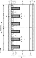
図1は、第1の実施形態の半導体装置の模式平面図である。第1の実施形態の半導体装置は、トレンチ構造を備えるRC−IGBT100である。
FIG. 1 is a schematic plan view of the semiconductor device according to the first embodiment. The semiconductor device of the first embodiment is an RC-
RC−IGBT100は、活性領域101と、活性領域101を囲む終端領域102を備える。活性領域101は、RC−IGBT100のオン動作時に電流を流す領域として機能する。終端領域102は、RC−IGBT100のオフ動作時に活性領域101の端部に印加される電界の強度を緩和し、RC−IGBT100の耐圧を向上させる領域として機能する。
The RC-IGBT 100 includes an
図2は、第1の実施形態の半導体装置の活性領域の模式平面図である。活性領域101は、複数のセルダイオード部111(第1のダイオード部)、リーディングダイオード部112(第2のダイオード部)、複数のセルIGBT部113(第1のIGBT部)を備える。なお、図2中の第1の方向と第2の方向は直交する。
FIG. 2 is a schematic plan view of the active region of the semiconductor device of the first embodiment. The
セルダイオード部111とセルIGBT部113は、第2の方向に隣り合って設けられる。セルダイオード部111とセルIGBT部113は、第2の方向に交互に配置される。
The
リーディングダイオード部112は、セルダイオード部111の第1の方向に隣り合って設けられる。また、セルIGBT部113は、リーディングダイオード部112の第1の方向に隣り合って設けられる。
The leading
図3は、第1の実施形態の半導体装置の活性領域の一部の模式断面図である。図2のA−A’断面を示す。図3は、セルダイオード部111とセルIGBT部113の断面図である。
FIG. 3 is a schematic cross-sectional view of a part of the active region of the semiconductor device of the first embodiment. 3 shows a cross section taken along the line A-A′ of FIG. 2. FIG. 3 is a cross-sectional view of the
セルダイオード部111には、ダイオードが設けられる。セルダイオード部111は、半導体層10、p型のアノード領域12(第1のアノード領域)、p+型のコンタクト領域14、n+型のカソード領域16(第1のカソード領域)、n−型のドリフト領域18、第1の共通電極20、第2の共通電極22を備える。また、トレンチ24(第1のトレンチ)、トレンチ絶縁膜26(第1のトレンチ絶縁膜)、トレンチ電極28(第1のトレンチ電極)を備える。
A diode is provided in the
半導体層10は、第1の面P1(以後、表面P1とも称する)と、第1の面に対向する第2の面P2(以後、裏面P2とも称する)を備える。半導体層10は、例えば、単結晶シリコンである。
The
p型のアノード領域12は、半導体層10の中に設けられる。アノード領域12は、p型不純物を含有する。p型不純物は、例えば、ボロン(B)である。
The p-
p+型のコンタクト領域14は、半導体層10の表面P1に接して設けられる。コンタクト領域14は、p型不純物を含有する。p型不純物は、例えば、ボロン(B)である。コンタクト領域14のp型不純物濃度は、アノード領域12のp型不純物濃度より高い。コンタクト領域14は、第1の共通電極20のコンタクト抵抗を低減する機能を備える。
The p +
n+型のカソード領域16は、アノード領域12と半導体層10の裏面P2との間に設けられる。カソード領域16は半導体層10の裏面P2に接して設けられる。カソード領域16は、n型不純物を含有する。n型不純物は、例えば、リン(P)又はヒ素(As)である。カソード領域16は、第2の共通電極22のコンタクト抵抗を低減する機能を備える。
The n +
n−型のドリフト領域18は、アノード領域12とカソード領域16との間に設けられる。ドリフト領域18は、n型不純物を含有する。n型不純物は、例えば、リン(P)である。
The n −
トレンチ24は、半導体層10の中に設けられる。トレンチ24は、半導体層10の第1の面側に設けられる。トレンチ24は、第1の方向に伸長する。トレンチ24は、アノード領域12を貫通し、底部はドリフト領域18に位置する。
The
トレンチ絶縁膜26は、トレンチ24の中に設けられる。トレンチ絶縁膜26は、例えば、酸化シリコンである。
The
トレンチ電極28は、トレンチ24の中に設けられる。トレンチ電極28は、トレンチ絶縁膜26の上に設けられる。トレンチ電極28は、第1の共通電極20に接する。トレンチ電極28は、第1の共通電極20及びアノード領域12に電気的に接続される。トレンチ電極28は、例えば、導電性不純物を含む多結晶シリコンである。
The
第1の共通電極20は、半導体層10の表面P1に設けられる。第1の共通電極20は、金属電極である。第1の共通電極20は、トレンチ電極28に接する。第1の共通電極20は、セルダイオード部111では、ダイオードのアノード電極として機能する。第1の共通電極20とコンタクト領域14との間のコンタクトは、オーミックコンタクトである。
The first
第2の共通電極22は、半導体層10の裏面P2に設けられる。第2の共通電極22は、金属電極である。第2の共通電極22は、セルダイオード部111では、ダイオードのカソード電極として機能する。第2の共通電極22とカソード領域16との間のコンタクトは、オーミックコンタクトである。
The second
セルIGBT部113には、IGBTが設けられる。セルIGBT部113は、半導体層10、n+型のエミッタ領域30(第1のエミッタ領域)、p+型のコンタクト領域32、p型のベース領域34(第1のベース領域)、p+型のコレクタ領域36(第1のコレクタ領域)、n−型のドリフト領域18、第1の共通電極20、第2の共通電極22を備える。また、トレンチ44(第3のトレンチ)、ゲート絶縁膜46(第1のゲート絶縁膜)、ゲート電極48(第1のゲート電極)、絶縁層49を備える。
An IGBT is provided in the
n+型のエミッタ領域30は、半導体層10の中に設けられる。n+型のエミッタ領域30は、半導体層10の表面P1に接して設けられる。n+型のエミッタ領域30は、n型不純物を含有する。n型不純物は、例えば、リン(P)又はヒ素(As)である。
The n +
p+型のコンタクト領域32は、半導体層10の表面P1に接して設けられる。コンタクト領域32は、p型不純物を含有する。p型不純物は、例えば、ボロン(B)である。コンタクト領域32のp型不純物濃度は、ベース領域34のp型不純物濃度より高い。コンタクト領域32は、第1の共通電極20のコンタクト抵抗を低減する機能を備える。また、コンタクト領域32は、ドリフト領域18に注入され蓄積された正孔を掃き出す機能を備える。
The p +
p+型のコレクタ領域36は、エミッタ領域30と半導体層10の裏面P2との間に設けられる。コレクタ領域36は半導体層10の裏面P2に接して設けられる。コレクタ領域36は、p型不純物を含有する。p型不純物は、例えば、ボロン(B)である。コレクタ領域36は、ホールをドリフト領域18に注入するとともに、第2の共通電極22のコンタクト抵抗を低減する機能を備える。
The p +
n−型のドリフト領域18は、エミッタ領域30とコレクタ領域36との間に設けられる。ドリフト領域18は、n型不純物を含有する。n型不純物は、例えば、リン(P)である。
The n −
p型のベース領域34は、エミッタ領域30とドリフト領域18との間に設けられる。p型のベース領域34は、p型不純物を含有する。p型不純物は、例えば、ボロン(B)である。p型のベース領域34は、IGBTのオン動作時に、反転層が形成され、チャネル領域として機能する。
The p-
p型のベース領域34は、例えば、セルダイオード部111のアノード領域12と同時に形成される。ベース領域34は、例えば、アノード領域12と略同一の不純物濃度、略同一の深さである。
The p-
なお、本明細書中、「深さ」とは、第1の面P1から、各領域の第2の面P2側の端部までの距離を意味する。 In the present specification, “depth” means the distance from the first surface P1 to the end of each region on the second surface P2 side.
なお、ここで、トレンチ44は、半導体層10の中の第1の方向(深さ方向)に伸長して設けられた、半導体層10の領域の一部を指す。トレンチ44は、半導体層10の第1の面P1側から、ベース領域34を貫通し、底部はドリフト領域18に達するように設けられる。
Here, the
ゲート絶縁膜46は、トレンチ24の中に設けられる。ゲート絶縁膜46は、は、例えば、酸化シリコンである。
The
ゲート電極48は、トレンチ44の中に設けられる。ゲート電極48は、ゲート絶縁膜46の上に設けられる。ゲート電極48に印加されるゲート電圧を制御することにより、IGBTのオンオフ動作を制御する。ゲート電極48は、例えば、導電性不純物を含む多結晶シリコンである。
The
第1の共通電極20は、セルIGBT部113では、IGBTのエミッタ電極として機能する。第1の共通電極20とエミッタ領域30との間のコンタクトは、オーミックコンタクトである。
In the
第2の共通電極22は、セルIGBT部113では、IGBTのコレクタ電極として機能する。第2の共通電極22とコレクタ領域36との間のコンタクトは、オーミックコンタクトである。
In the
絶縁層49は、第1の共通電極20とゲート電極48との間に設けられる。絶縁層49は、第1の共通電極20とゲート電極48とを電気的に分離する。
The insulating
図4は、第1の実施形態の半導体装置の活性領域の一部の模式断面図である。図2のB−B’断面を示す。図4は、リーディングダイオード部112の断面図である。
FIG. 4 is a schematic cross-sectional view of a part of the active region of the semiconductor device of the first embodiment. 3 shows a B-B′ cross section of FIG. 2. FIG. 4 is a sectional view of the leading
リーディングダイオード部112には、ダイオードが設けられる。RC−IGBT100がゲート電極に正電圧が印加された状態で逆導通モードになる際に、リーディングダイオード部112のダイオードは、セルダイオード部111のダイオードに先行してオン動作する機能を有する。
A diode is provided in the leading
リーディングダイオード部112は、半導体層10、p型のアノード領域52(第2のアノード領域)、p+型のコンタクト領域54、n+型のカソード領域56(第2のカソード領域)、n−型のドリフト領域18、第1の共通電極20、第2の共通電極22を備える。また、トレンチ64(第2のトレンチ)、トレンチ絶縁膜66(第2のトレンチ絶縁膜)、トレンチ電極68(第2のトレンチ電極)を備える。
The leading
リーディングダイオード部112のp型のアノード領域52(第2のアノード領域)、p+型のコンタクト領域54、n+型のカソード領域56(第2のカソード領域)、トレンチ64(第2のトレンチ)、トレンチ絶縁膜66(第2のトレンチ絶縁膜)、トレンチ電極68(第2のトレンチ電極)は、それぞれ、セルダイオード部111のp型のアノード領域12(第1のアノード領域)、p+型のコンタクト領域14、n+型のカソード領域16(第1のカソード領域)、トレンチ24(第1のトレンチ)、トレンチ絶縁膜26(第1のトレンチ絶縁膜)、トレンチ電極28(第1のトレンチ電極)と同様の構成及び機能を有する。
The p-type anode region 52 (second anode region), p + -
第1の共通電極20は、リーディングダイオード部112では、ダイオードのアノード電極として機能する。第2の共通電極22は、リーディングダイオード部112では、ダイオードのカソード電極として機能する。
In the leading
リーディングダイオード部112の第1の方向の幅(図2中のW2)は、セルダイオード部111の第2の方向の幅(図2中のW1)よりも大きい。リーディングダイオード部112の第1の方向の幅(図2中のW2)は、例えば、60μm以上である。
The width of the leading
図5は、第1の実施形態の半導体装置の活性領域の模式平面図である。図5は、セルダイオード部111のトレンチ24(第1のトレンチ)、リーディングダイオード部112のトレンチ64(第2のトレンチ)、セルIGBT部113のトレンチ44(第3のトレンチ)のレイアウトパターンを示す図である。
FIG. 5 is a schematic plan view of the active region of the semiconductor device of the first embodiment. FIG. 5 shows a layout pattern of the trench 24 (first trench) of the
トレンチ24、トレンチ64、トレンチ44は、第1の方向に伸長する。トレンチ24とトレンチ64は連続している。トレンチ24とトレンチ64が連続することで、トレンチ24の中のトレンチ電極28と、トレンチ64の中のトレンチ電極68が接続されている。
The
トレンチ64とトレンチ44は離間している。トレンチ64とトレンチ44が離間することで、トレンチ64の中のトレンチ電極68と、トレンチ44の中のゲート電極48が分離している。
The
図6は、第1の実施形態の半導体装置の活性領域の模式平面図である。図6は、セルダイオード部111のn+型のカソード領域16(第1のカソード領域)、リーディングダイオード部112のn+型のカソード領域56(第2のカソード領域)、セルIGBT部113のp+型のコレクタ領域36のレイアウトパターンを示す図である。
FIG. 6 is a schematic plan view of the active region of the semiconductor device of the first embodiment. 6, the cathode region 16 (the first cathode region) of the n + -
n+型のカソード領域16とp+型のコレクタ領域36は、第2の方向に交互に配置される。n+型のカソード領域16とp+型のコレクタ領域36は、物理的に接続されている。
The n +
n+型のカソード領域56は、n+型のカソード領域16の第1の方向に配置される。n+型のカソード領域56は、p+型のコレクタ領域36の第1の方向に配置される。n+型のカソード領域56とn+型のカソード領域16は物理的に接続される。
The n +
次に、第1の実施形態の作用及び効果について説明する。 Next, the operation and effect of the first embodiment will be described.
図7は、比較例の半導体装置の活性領域の模式平面図である。比較例の半導体装置は、トレンチ構造を備えるRC−IGBTである。 FIG. 7 is a schematic plan view of the active region of the semiconductor device of the comparative example. The semiconductor device of the comparative example is an RC-IGBT having a trench structure.
比較例のRC−IGBTは、活性領域901を備える。活性領域901は、複数のセルダイオード部111、複数のセルIGBT部113を備える。比較例のRC−IGBTは、リーディングダイオード部112を備えない点で第1の実施形態のRC−IGBT100と異なる。セルダイオード部111、セルIGBT部113の構成は第1の実施形態のRC−IGBT100と同様である。
The RC-IGBT of the comparative example includes an
図8は、比較例の半導体装置の電流電圧特性を示す図である。図8は、比較例のRC−IGBTがゲート電極に正電圧が印加された状態で逆導通モードになる場合の電流電圧特性を示す。実線が比較例の場合の電流電圧特性、点線が理想的な電流電圧特性である。 FIG. 8 is a diagram showing current-voltage characteristics of the semiconductor device of the comparative example. FIG. 8 shows current-voltage characteristics when the RC-IGBT of the comparative example is in the reverse conduction mode with a positive voltage applied to the gate electrode. The solid line shows the current-voltage characteristic in the comparative example, and the dotted line shows the ideal current-voltage characteristic.
RC−IGBTの逆導通モードでは、セルダイオード部111のダイオードが順方向動作する。理想的には、電流が順方向電圧(Vf)で急速に立ち上がる。しかし、比較例のRC−IGBTでは、一定の電圧まで電流の急速な立ち上がりが抑制される現象、いわゆるスナップバックが生じる。
In the reverse conduction mode of the RC-IGBT, the diode of the
セルダイオード部111で、スナップバックが生じると、例えば、複数のRC−IGBTを並列接続している場合に、それぞれのRC−IGBTを流れる電流のアンバランスが生じ得る。電流のアンバランスが生じると、特定のRC−IGBTに過剰な電流が流れて、特定のRC−IGBTが破壊するおそれがある。
If snapback occurs in the
図9は、比較例の半導体装置の活性領域の一部の模式断面図である。図7のC−C’断面を示す。図9は、セルダイオード部111とセルIGBT部113の断面図である。
FIG. 9 is a schematic cross-sectional view of a part of the active region of the semiconductor device of the comparative example. FIG. 8 shows a C-C′ cross section of FIG. 7. FIG. 9 is a cross-sectional view of the
RC−IGBTの逆導通モードの場合は、第2の共通電極22に対し、第1の共通電極20に相対的に正電圧が印加される。RC−IGBTの逆導通モードでは、セルIGBT部113のゲート電極48には、IGBTのオン動作時のゲート電圧が印加される場合がある。この場合、ベース領域34には、反転層が形成され、チャネル領域が形成される。
In the case of the reverse conduction mode of the RC-IGBT, a positive voltage is applied relatively to the first
セルIGBT部113のIGBTにチャネル領域が形成されることで、第2の共通電極22から、カソード領域16、ドリフト領域18、ベース領域34、エミッタ領域30を経由して第1の共通電極20に至る電子のパスが形成される。したがって、セルダイオード部111の電子が、セルIGBT部113から排出される。よって、セルダイオード部111のキャリア濃度が上昇せず、セルダイオード部111のダイオードの電流の立ち上がりが抑制され、スナップバックが生じると考えられる。
Since the channel region is formed in the IGBT of the
第1の実施形態のRC−IGBT100では、リーディングダイオード部112を新たに設ける。リーディングダイオード部112の第1の方向の幅(図2中のW2)は、セルダイオード部111の第2の方向の幅(図2中のW1)よりも大きい。リーディングダイオード部112は、セルIGBT部113からの距離が遠い領域を備えている。
In the RC-
セルIGBT部113からの距離が遠い領域では、逆導通モードの場合にセルIGBT部113からの電子の排出が抑制され、ダイオードのスナップバックが抑制される。したがって、リーディングダイオード部112のダイオードは、図8に点線で示すような、電流が順方向電圧(Vf)で急速に立ち上がる理想的な電流電圧特性を備えることになる。
In a region far from the
リーディングダイオード部112のダイオードの電流電圧特性が順方向電圧(Vf)で急速に立ち上がると、リーディングダイオード部112からリーディングダイオード部112に接続されるセルダイオード部111にキャリアが供給される。したがって、セルダイオード部111の電流も順方向電圧(Vf)で急速に立ち上がるようになる。言い換えれば、セルダイオード部111でのスナップバックも抑制され、セルダイオード部111でも、電流が順方向電圧(Vf)で急速に立ち上がる理想的な電流電圧特性を備えることになる。
When the current-voltage characteristic of the diode of the leading
リーディングダイオード部112の第1の方向の幅(図2中のW2)は、60μm以上であることが好ましい。セルIGBT部113から60μm以上離れると、ダイオードのスナップバックが十分に抑制されることが、デバイスシュミレーションの結果から明らかになっている。第1の実施形態のRC−IGBT100のようにリーディングダイオード部112の両側にセルIGBT部113が存在する場合は、リーディングダイオード部112の第1の方向の幅(図2中のW2)は、120μm以上であることが好ましい。
The width of the leading
第1の実施形態によれば、逆導通モードの場合のダイオードのスナップバックが抑制されたRC−IGBT100が実現できる。
According to the first embodiment, it is possible to realize the RC-
(第2の実施形態)
第2の実施形態の半導体装置は、第1のコレクタ領域が第1のダイオード部に設けられた点で、第1の実施形態と異なる。以下、第1の実施形態と重複する内容については、一部記述を省略する。
(Second embodiment)
The semiconductor device of the second embodiment is different from that of the first embodiment in that the first collector region is provided in the first diode portion. Hereinafter, a part of the description overlapping with that of the first embodiment will be omitted.
第2の実施形態のRC−IGBTは、カソード領域16、カソード領域56、コレクタ領域36のレイアウトパターンが異なる以外は第1の実施形態と同様である。
The RC-IGBT of the second embodiment is the same as that of the first embodiment except that the layout patterns of the
図10は、第2の実施形態の半導体装置の活性領域の模式平面図である。第2の実施形態の半導体装置は、トレンチ構造を備えるRC−IGBTである。 FIG. 10 is a schematic plan view of the active region of the semiconductor device of the second embodiment. The semiconductor device of the second embodiment is an RC-IGBT having a trench structure.
活性領域201は、複数のセルダイオード部111(第1のダイオード部)、リーディングダイオード部112(第2のダイオード部)、複数のセルIGBT部113(第1のIGBT部)を備える。
The
図10には、セルダイオード部111のn+型のカソード領域16(第1のカソード領域)、リーディングダイオード部112のn+型のカソード領域56(第2のカソード領域)、セルIGBT部113のp+型のコレクタ領域36のレイアウトパターンを示す。
Figure 10 is, n + -
セルIGBT部113のp+型のコレクタ領域36が、セルダイオード部111にも設けられる。セルダイオード部111の裏面P2にもp+型のコレクタ領域36が存在する。
The p +
また、セルダイオード部111のn+型のカソード領域16が、セルIGBT部113に設けられる。セルIGBT部113の裏面P2にもn+型のカソード領域16が存在する。
Further, the n +
n+型のカソード領域16とp+型のコレクタ領域36は、第1の方向に交互に配置される。n+型のカソード領域16とp+型のコレクタ領域36は、接続されている。
The n +
第2の実施形態のRC−IGBTでは、セルダイオード部111の裏面P2にもp+型のコレクタ領域36が存在する。これにより、セルIGBT部113のIGBTのオン動作時に、セルダイオード部111にもIGBTのオン電流が流れる。言い換えれば、セルダイオード部111もIGBTの有効領域として機能する。したがって、RC−IGBTのオン動作時のオン電流が増加する。
In the RC-IGBT of the second embodiment, the p + -
第2の実施形態によれば、第1の実施形態同様、逆導通モードの場合のダイオードのスナップバックが抑制されたRC−IGBTが実現できる。更に、オン動作時のオン電流が増加したRC−IGBTが実現できる。 According to the second embodiment, the RC-IGBT in which the snapback of the diode in the reverse conduction mode is suppressed can be realized as in the first embodiment. Furthermore, an RC-IGBT with an increased on-current during the on-operation can be realized.
(第3の実施形態)
第3の実施形態の半導体装置は、第2のIGBT部を更に、備え、第2のIGBT部は、第1のダイオード部及び第2のダイオード部の第2の方向に隣り合って設けられ、半導体層の中に設けられた第2導電型の第2のエミッタ領域と、第2のエミッタ領域と第2の面との間に設けられた第1導電型の第2のコレクタ領域と、第2のエミッタ領域と第2のコレクタ領域との間に設けられたドリフト領域と、第2のエミッタ領域とドリフト領域との間に設けられた第1導電型の第2のベース領域と、半導体層の中に設けられて第1の方向に伸長する第4のトレンチと、第4のトレンチの中に設けられた第2のゲート絶縁膜と、第4のトレンチの中であって第2のゲート絶縁膜の上に設けられた第2のゲート電極と、を有し、第2のコレクタ領域と第1のコレクタ領域が物理的に接続され、第2のコレクタ領域の第2の方向の幅が第1のコレクタ領域の第1の方向の幅よりも大きい点で、第1の実施形態と異なる。以下、第1の実施形態と重複する内容については、一部記述を省略する。
(Third Embodiment)
The semiconductor device according to the third embodiment further includes a second IGBT section, and the second IGBT section is provided adjacent to the first diode section and the second diode section in the second direction, A second emitter region of the second conductivity type provided in the semiconductor layer; a second collector region of the first conductivity type provided between the second emitter region and the second surface; Drift region provided between the second emitter region and the second collector region, a second base region of the first conductivity type provided between the second emitter region and the drift region, and a semiconductor layer A fourth trench provided in the first trench and extending in the first direction, a second gate insulating film provided in the fourth trench, and a second gate in the fourth trench A second gate electrode provided on the insulating film, the second collector region and the first collector region are physically connected, and the width of the second collector region in the second direction is It is different from the first embodiment in that it is larger than the width of the first collector region in the first direction. Hereinafter, a part of the description overlapping with that of the first embodiment will be omitted.
図11は、第3の実施形態の半導体装置の活性領域の模式平面図である。第3の実施形態の半導体装置は、トレンチ構造を備えるRC−IGBTである。 FIG. 11 is a schematic plan view of the active region of the semiconductor device of the third embodiment. The semiconductor device of the third embodiment is an RC-IGBT having a trench structure.
活性領域301は、複数のセルダイオード部111(第1のダイオード部)、リーディングダイオード部112(第2のダイオード部)、複数のセルIGBT部113(第1のIGBT部)、リーディングIGBT部114(第2のIGBT部)を備える。なお、第1の方向と第2の方向は直交する。
The
セルダイオード部111とセルIGBT部113は、第2の方向に隣り合って設けられる。セルダイオード部111とセルIGBT部113は、第2の方向に交互に配置される。
The
リーディングダイオード部112は、セルダイオード部111の第1の方向に隣り合って設けられる。また、セルIGBT部113は、リーディングダイオード部112の第1の方向に隣り合って設けられる。
The leading
リーディングIGBT部114は、セルダイオード部111及びリーディングダイオード部112の第2の方向に隣り合って設けられる。
The leading
図12は、第3の実施形態の半導体装置の活性領域の一部の模式断面図である。図12は、図11のD−D’断面を示す。図12は、リーディングIGBT部114の断面図である。
FIG. 12 is a schematic cross-sectional view of a part of the active region of the semiconductor device of the third embodiment. FIG. 12 shows a D-D′ cross section of FIG. 11. FIG. 12 is a sectional view of the leading
リーディングIGBT部114には、IGBTが設けられる。リーディングIGBT部114は、半導体層10、n+型のエミッタ領域70(第2のエミッタ領域)、p+型のコンタクト領域72、p型のベース領域74(第2のベース領域)、p+型のコレクタ領域76(第2のコレクタ領域)、n−型のドリフト領域18、第1の共通電極20、第2の共通電極22を備える。また、トレンチ84(第4のトレンチ)、ゲート絶縁膜86(第2のゲート絶縁膜)、ゲート電極88(第2のゲート電極)、絶縁層89を備える。
An IGBT is provided in the leading
リーディングIGBT部114のn+型のエミッタ領域70(第2のエミッタ領域)、p+型のコンタクト領域72、p型のベース領域74(第2のベース領域)、p+型のコレクタ領域76(第2のコレクタ領域)、トレンチ84(第4のトレンチ)、ゲート絶縁膜86(第2のゲート絶縁膜)、ゲート電極88(第2のゲート電極)、絶縁層89は、セルIGBT部113のn+型のエミッタ領域30(第1のエミッタ領域)、p+型のコンタクト領域32、p型のベース領域34(第1のベース領域)、p+型のコレクタ領域36(第1のコレクタ領域)、トレンチ44(第3のトレンチ)、ゲート絶縁膜46(第1のゲート絶縁膜)、ゲート電極48(第1のゲート電極)、絶縁層49と同様の構成及び機能を有する。
The n + type emitter region 70 (second emitter region) of the leading
図13は、第3の実施形態の半導体装置の模式平面図である。図13は、セルダイオード部111のn+型のカソード領域16(第1のカソード領域)、リーディングダイオード部112のn+型のカソード領域56(第2のカソード領域)、セルIGBT部113のp+型のコレクタ領域36(第1のコレクタ領域)、リーディングIGBT部114のp+型のコレクタ領域76(第2のコレクタ領域)のレイアウトパターンを示す図である。
FIG. 13 is a schematic plan view of the semiconductor device according to the third embodiment. Figure 13 is a cathode region 16 (the first cathode region) of the n + -
セルIGBT部113のp+型のコレクタ領域36が、セルダイオード部111に伸長している。セルダイオード部111にもp+型のコレクタ領域36が存在する。
The p +
また、セルダイオード部111のn+型のカソード領域16が、セルIGBT部113に伸長している。セルIGBT部113にもn+型のカソード領域16が存在する。
Further, the n +
n+型のカソード領域16とp+型のコレクタ領域36は、第1の方向に交互に配置される。n+型のカソード領域16とp+型のコレクタ領域36は、物理的に接続されている。
The n +
p+型のコレクタ領域76とp+型のコレクタ領域36は物理的に接続される。p+型のコレクタ領域76とn+型のカソード領域16は物理的に接続される。
The p +
p+型のコレクタ領域76の第2の方向の幅(図13中のW4)は、p+型のコレクタ領域36の第1の方向の幅(図13中のW3)よりも大きい。
The width of the p + -
次に、第3の実施形態の作用及び効果について説明する。 Next, the operation and effect of the third embodiment will be described.
例えば、第2の実施形態のRC−IGBTがオン動作する場合には、第1の共通電極20に対し、第2の共通電極22に相対的に正電圧が印加される。また、ゲート電極48には、ベース領域34にチャネル領域が形成されるように正のゲート電圧が印加される。
For example, when the RC-IGBT of the second embodiment is turned on, a positive voltage is applied to the second
第2の実施形態のRC−IGBTでは、セルIGBT部113がオン動作をする際に、第1の共通電極20から、セルIGBT部113のエミッタ領域30、ベース領域34、ドリフト領域18、カソード領域16を経由して第2の共通電極22に至る電子のパスが形成される。したがって、セルIGBT部113の電子が、第2の共通電極22から排出される。よって、セルIGBT部113のキャリア濃度が上昇せず、セルIGBT部113のIGBTの電流の立ち上がりが抑制され、スナップバックが生じる。
In the RC-IGBT of the second embodiment, when the
セルIGBT部113で、スナップバックが生じると、例えば、複数のRC−IGBTを並列接続している場合に、それぞれのRC−IGBTを流れる電流のアンバランスが生じ得る。電流のアンバランスが生じると、特定のRC−IGBTに過剰な電流が流れて、特定のRC−IGBTが破壊するおそれがある。
If snapback occurs in the
第3の実施形態のRC−IGBTでは、第2の実施形態のRC−IGBTに対し、リーディングIGBT部114を新たに設ける。リーディングIGBT部114のp+型のコレクタ領域76の第2の方向の幅(図13中のW4)は、セルIGBT部113のp+型のコレクタ領域36の第1の方向の幅(図13中のW3)よりも大きい。リーディングIGBT部114は、n+型のカソード領域16からの距離が遠いp+型のコレクタ領域76を有する領域を備えている。
In the RC-IGBT of the third embodiment, a leading
リーディングIGBT部114のカソード領域16からの距離が遠いp+型のコレクタ領域76を有する領域では、IGBTがオン動作する際に、第2の共通電極22からの電子の排出が抑制される。したがって、リーディングIGBT部114のIGBTのスナップバックが抑制される。
In the region having the p + -
リーディングIGBT部114のIGBTがオン動作し、電流が急速に流れるようになると、リーディングIGBT部114にp+型のコレクタ領域36で接続されるセルIGBT部113にキャリアが供給される。これにより、セルIGBT部113のIGBTもオン動作し電流が急速に立ち上がることになる。したがって、セルIGBT部113のIGBTのスナップバックも抑制される。
When the IGBT of the leading
リーディングIGBT部114のp+型のコレクタ領域76の第2の方向の幅(図13中のW4)は、600μm以上であることが好ましい。p+型のコレクタ領域76が、n+型のカソード領域16から600μm以上離れると、IGBTのスナップバックが十分に抑制されることが、デバイスシュミレーションの結果から明らかになっている。
The width of the p + -
第3の実施形態によれば、第1の実施形態同様、逆導通モードの場合のダイオードのスナップバックが抑制されたRC−IGBTが実現できる。また、第2の実施形態同様、オン動作時のオン電流が増加したRC−IGBTが実現できる。更に、IGBTのスナップバックが抑制されたRC−IGBTが実現できる。 According to the third embodiment, as in the first embodiment, it is possible to realize an RC-IGBT in which snapback of the diode in the reverse conduction mode is suppressed. Further, as in the second embodiment, it is possible to realize the RC-IGBT in which the on-current during the on-operation is increased. Furthermore, an RC-IGBT in which snapback of the IGBT is suppressed can be realized.
以上、実施形態では、半導体層10がシリコンである場合を例に説明したが、半導体層10は、SiC、GaN系半導体など、その他の半導体であってもかまわない。
As described above, in the embodiment, the case where the
また、実施形態では、第1導電型がp型、第2導電型がn型の場合を例に説明したが、第1導電型をn型、第2導電型をp型とすることも可能である。 In the embodiment, the case where the first conductivity type is p-type and the second conductivity type is n-type has been described as an example, but the first conductivity type may be n-type and the second conductivity type may be p-type. Is.
本発明のいくつかの実施形態を説明したが、これらの実施形態は、例として提示したものであり、発明の範囲を限定することは意図していない。これら新規な実施形態は、その他の様々な形態で実施されることが可能であり、発明の要旨を逸脱しない範囲で、種々の省略、置き換え、変更を行うことができる。例えば、一実施形態の構成要素を他の実施形態の構成要素と置き換え又は変更してもよい。これら実施形態やその変形は、発明の範囲や要旨に含まれるとともに、特許請求の範囲に記載された発明とその均等の範囲に含まれる。 Although some embodiments of the present invention have been described, these embodiments are presented as examples and are not intended to limit the scope of the invention. These novel embodiments can be implemented in various other forms, and various omissions, replacements, and changes can be made without departing from the spirit of the invention. For example, the components of one embodiment may be replaced or changed with the components of another embodiment. These embodiments and their modifications are included in the scope and gist of the invention, and are also included in the invention described in the claims and the scope of equivalents thereof.
10 半導体層
12 p型のアノード領域(第1のアノード領域)
16 n+型のカソード領域(第1のカソード領域)
18 n−型のドリフト領域
24 トレンチ(第1のトレンチ)
26 トレンチ絶縁膜(第1のトレンチ絶縁膜)
28 トレンチ電極(第1のトレンチ電極)
30 n+型のエミッタ領域(第1のエミッタ領域)
34 p型のベース領域(第1のベース領域)
36 p+型のコレクタ領域(第1のコレクタ領域)
44 トレンチ(第3のトレンチ)
46 ゲート絶縁膜(第1のゲート絶縁膜)
48 ゲート電極(第1のゲート電極)
52 p型のアノード領域(第2のアノード領域)
56 n+型のカソード領域(第2のカソード領域)
64 トレンチ(第2のトレンチ)
66 トレンチ絶縁膜(第2のトレンチ絶縁膜)
68 トレンチ電極(第2のトレンチ電極)
70 n+型のエミッタ領域(第2のエミッタ領域)
74 p型のベース領域(第2のベース領域)
76 p+型のコレクタ領域(第2のコレクタ領域)
84 トレンチ(第4のトレンチ)
86 ゲート絶縁膜(第2のゲート絶縁膜)
88 ゲート電極(第2のゲート電極)
100 RC−IGBT(半導体装置)
111 セルダイオード部(第1のダイオード部)
112 リーディングダイオード部(第2のダイオード部)
113 セルIGBT部(第1のIGBT部)
114 リーディングIGBT部(第2のIGBT部)
10 semiconductor layer 12 p-type anode region (first anode region)
16 n + type cathode region (first cathode region)
18 n −
26 Trench Insulating Film (First Trench Insulating Film)
28 Trench electrode (first trench electrode)
30 n + type emitter region (first emitter region)
34 p-type base region (first base region)
36 p + type collector region (first collector region)
44 trench (third trench)
46 Gate insulating film (first gate insulating film)
48 gate electrode (first gate electrode)
52 p-type anode region (second anode region)
56 n + type cathode region (second cathode region)
64 trench (second trench)
66 Trench insulating film (second trench insulating film)
68 Trench electrode (second trench electrode)
70 n + type emitter region (second emitter region)
74 p-type base region (second base region)
76 p + type collector region (second collector region)
84 Trench (4th trench)
86 Gate insulating film (second gate insulating film)
88 gate electrode (second gate electrode)
100 RC-IGBT (semiconductor device)
111 cell diode section (first diode section)
112 Leading diode part (second diode part)
113-cell IGBT unit (first IGBT unit)
114 Leading IGBT part (second IGBT part)
Claims (9)
前記第1のアノード領域と前記第2の面との間に設けられた第2導電型の第1のカソード領域と、
前記第1のアノード領域と前記第1のカソード領域との間に設けられ、前記第1のカソード領域よりも第2導電型の不純物濃度の低い第2導電型のドリフト領域と、
前記半導体層の中に設けられて第1の方向に伸長する第1のトレンチと、
前記第1のトレンチの中に設けられた第1のトレンチ絶縁膜と、
前記第1のトレンチの中であって、前記第1のトレンチ絶縁膜の上に設けられ、前記第1のアノード領域に電気的に接続された第1のトレンチ電極と、を有する第1のダイオード部と、
前記半導体層の中に設けられた第1導電型の第2のアノード領域と、
前記第2のアノード領域と前記第2の面との間に設けられた第2導電型の第2のカソード領域と、
前記第2のアノード領域と前記第2のカソード領域との間に設けられた前記ドリフト領域と、
前記半導体層の中に設けられて前記第1の方向に伸長する第2のトレンチと、
前記第2のトレンチの中に設けられた第2のトレンチ絶縁膜と、
第2のトレンチの中であって、前記第2のトレンチ絶縁膜の上に設けられ、前記第2のアノード領域に電気的に接続された第2のトレンチ電極と、を有し、
前記第1の方向の幅が、前記第1のダイオード部の前記第1の方向に直交する第2の方向の幅よりも大きく、
前記第1のダイオード部の前記第1の方向に隣り合って設けられた第2のダイオード部と、
前記半導体層の中に設けられた第2導電型の第1のエミッタ領域と、
前記第1のエミッタ領域と前記第2の面との間に設けられた第1導電型の第1のコレクタ領域と、
前記第1のエミッタ領域と前記第1のコレクタ領域との間に設けられた前記ドリフト領域と、
前記第1のエミッタ領域と前記ドリフト領域との間に設けられた第1導電型の第1のベース領域と、
前記半導体層の中に設けられて前記第1の方向に伸長する第3のトレンチと、
前記第3のトレンチの中に設けられた第1のゲート絶縁膜と、
前記第3のトレンチの中であって、前記第1のゲート絶縁膜の上に設けられた第1のゲート電極と、を有し、
前記第1のダイオード部の前記第2の方向に隣り合って設けられ、前記第2のダイオード部の前記第1の方向に隣り合って設けられた第1のIGBT部と、
を備える半導体装置。 A first conductivity type first anode region provided in the semiconductor layer having a first surface and a second surface;
A second cathode of a second conductivity type provided between the first anode region and the second surface;
A second conductive type drift region provided between the first anode region and the first cathode region and having a second conductive type impurity concentration lower than that of the first cathode region;
A first trench provided in the semiconductor layer and extending in a first direction;
A first trench insulating film provided in the first trench;
A first trench electrode in the first trench, the first trench electrode provided on the first trench insulating film and electrically connected to the first anode region; Department,
A second anode region of the first conductivity type provided in the semiconductor layer;
A second cathode region of the second conductivity type provided between the second anode region and the second surface;
The drift region provided between the second anode region and the second cathode region;
A second trench provided in the semiconductor layer and extending in the first direction;
A second trench insulating film provided in the second trench;
A second trench electrode provided in the second trench on the second trench insulating film and electrically connected to the second anode region;
The width in the first direction is larger than the width in the second direction orthogonal to the first direction of the first diode portion,
A second diode portion provided adjacent to the first diode portion in the first direction;
A first emitter region of a second conductivity type provided in the semiconductor layer,
A first collector region of a first conductivity type provided between the first emitter region and the second surface;
The drift region provided between the first emitter region and the first collector region;
A first base region of a first conductivity type provided between the first emitter region and the drift region,
A third trench provided in the semiconductor layer and extending in the first direction;
A first gate insulating film provided in the third trench;
A first gate electrode provided on the first gate insulating film in the third trench,
A first IGBT section provided adjacent to the first diode section in the second direction, and provided adjacent to the second diode section in the first direction;
A semiconductor device comprising:
前記第2のIGBT部は、
前記第1のダイオード部及び前記第2のダイオード部の前記第2の方向に隣り合って設けられ、
前記半導体層の中に設けられた第2導電型の第2のエミッタ領域と、
前記第2のエミッタ領域と前記第2の面との間に設けられた第1導電型の第2のコレクタ領域と、
前記第2のエミッタ領域と前記第2のコレクタ領域との間に設けられた前記ドリフト領域と、
前記第2のエミッタ領域と前記ドリフト領域との間に設けられた第1導電型の第2のベース領域と、
前記半導体層の中に設けられて前記第1の方向に伸長する第4のトレンチと、
前記第4のトレンチの中に設けられた第2のゲート絶縁膜と、
前記第4のトレンチの中であって、前記第2のゲート絶縁膜の上に設けられた第2のゲート電極と、を有し、
前記第2のコレクタ領域と前記第1のコレクタ領域が接続され、
前記第2のコレクタ領域の前記第2の方向の幅が前記第1のコレクタ領域の前記第1の方向の幅よりも大きい請求項1乃至請求項7いずれか一項記載の半導体装置。 Further comprising a second IGBT section,
The second IGBT section,
The first diode portion and the second diode portion are provided adjacent to each other in the second direction,
A second emitter region of the second conductivity type provided in the semiconductor layer;
A second collector region of the first conductivity type provided between the second emitter region and the second surface;
The drift region provided between the second emitter region and the second collector region;
A second base region of the first conductivity type provided between the second emitter region and the drift region;
A fourth trench provided in the semiconductor layer and extending in the first direction;
A second gate insulating film provided in the fourth trench;
A second gate electrode provided on the second gate insulating film in the fourth trench,
The second collector region and the first collector region are connected,
8. The semiconductor device according to claim 1, wherein a width of the second collector region in the second direction is larger than a width of the first collector region in the first direction.
Priority Applications (3)
| Application Number | Priority Date | Filing Date | Title |
|---|---|---|---|
| JP2017176263A JP6736531B2 (en) | 2017-09-14 | 2017-09-14 | Semiconductor device |
| US15/912,600 US10418470B2 (en) | 2017-09-14 | 2018-03-06 | Semiconductor device having IGBT portion and diode portion |
| CN201810181594.9A CN109509789B (en) | 2017-09-14 | 2018-03-06 | Semiconductor device with a plurality of semiconductor chips |
Applications Claiming Priority (1)
| Application Number | Priority Date | Filing Date | Title |
|---|---|---|---|
| JP2017176263A JP6736531B2 (en) | 2017-09-14 | 2017-09-14 | Semiconductor device |
Publications (3)
| Publication Number | Publication Date |
|---|---|
| JP2019054070A JP2019054070A (en) | 2019-04-04 |
| JP2019054070A5 JP2019054070A5 (en) | 2019-09-19 |
| JP6736531B2 true JP6736531B2 (en) | 2020-08-05 |
Family
ID=65631494
Family Applications (1)
| Application Number | Title | Priority Date | Filing Date |
|---|---|---|---|
| JP2017176263A Active JP6736531B2 (en) | 2017-09-14 | 2017-09-14 | Semiconductor device |
Country Status (3)
| Country | Link |
|---|---|
| US (1) | US10418470B2 (en) |
| JP (1) | JP6736531B2 (en) |
| CN (1) | CN109509789B (en) |
Families Citing this family (7)
| Publication number | Priority date | Publication date | Assignee | Title |
|---|---|---|---|---|
| JP7061983B2 (en) * | 2019-04-26 | 2022-05-02 | 三菱電機株式会社 | Semiconductor device |
| EP3748851B1 (en) * | 2019-06-07 | 2023-03-15 | Infineon Technologies AG | Semiconductor device and semiconductor arrangement comprising semiconductor devices |
| DE102019133030B4 (en) * | 2019-12-04 | 2023-05-04 | Infineon Technologies Austria Ag | INSULATED GATE BIPOLAR TRANSISTOR INCLUDING SEMICONDUCTOR DEVICE AND METHOD OF MANUFACTURE |
| DE102019135545A1 (en) * | 2019-12-20 | 2021-06-24 | Infineon Technologies Ag | Power semiconductor device |
| CN111211167B (en) * | 2020-01-09 | 2022-04-01 | 杭州电子科技大学 | RC-IGBT device structure for eliminating negative resistance effect |
| JP7198236B2 (en) * | 2020-03-13 | 2022-12-28 | 株式会社東芝 | semiconductor equipment |
| JP2022116567A (en) | 2021-01-29 | 2022-08-10 | 株式会社東芝 | Semiconductor device |
Family Cites Families (33)
| Publication number | Priority date | Publication date | Assignee | Title |
|---|---|---|---|---|
| JPS539176B2 (en) | 1973-08-28 | 1978-04-04 | ||
| JP3973832B2 (en) * | 2000-11-10 | 2007-09-12 | 株式会社東芝 | Pressure contact type semiconductor device |
| DE10122364B4 (en) * | 2001-05-09 | 2006-10-19 | Infineon Technologies Ag | Compensation component, circuit arrangement and method |
| GB0122120D0 (en) * | 2001-09-13 | 2001-10-31 | Koninkl Philips Electronics Nv | Edge termination in MOS transistors |
| JP5103830B2 (en) * | 2006-08-28 | 2012-12-19 | 三菱電機株式会社 | Insulated gate semiconductor device |
| JP5206541B2 (en) * | 2008-04-01 | 2013-06-12 | 株式会社デンソー | Semiconductor device and manufacturing method thereof |
| US20100117117A1 (en) * | 2008-11-10 | 2010-05-13 | Infineon Technologies Ag | Vertical IGBT Device |
| JP2010135646A (en) * | 2008-12-05 | 2010-06-17 | Toyota Central R&D Labs Inc | Semiconductor device |
| US8304829B2 (en) * | 2008-12-08 | 2012-11-06 | Fairchild Semiconductor Corporation | Trench-based power semiconductor devices with increased breakdown voltage characteristics |
| JP5045733B2 (en) | 2008-12-24 | 2012-10-10 | 株式会社デンソー | Semiconductor device |
| JP5432750B2 (en) * | 2010-02-01 | 2014-03-05 | ルネサスエレクトロニクス株式会社 | Semiconductor device and manufacturing method of semiconductor device |
| JP5900546B2 (en) * | 2010-07-01 | 2016-04-06 | 株式会社デンソー | Semiconductor device |
| JP2013074181A (en) * | 2011-09-28 | 2013-04-22 | Toyota Motor Corp | Semiconductor device and manufacturing method of the same |
| JP6022774B2 (en) * | 2012-01-24 | 2016-11-09 | トヨタ自動車株式会社 | Semiconductor device |
| US8866222B2 (en) * | 2012-03-07 | 2014-10-21 | Infineon Technologies Austria Ag | Charge compensation semiconductor device |
| JP2014075582A (en) | 2012-09-12 | 2014-04-24 | Fuji Electric Co Ltd | Semiconductor device and method of manufacturing semiconductor device |
| KR101876579B1 (en) * | 2012-09-13 | 2018-07-10 | 매그나칩 반도체 유한회사 | Power Semiconductor and Fabricating Method Thereof |
| CN104995738B (en) * | 2013-08-15 | 2018-01-23 | 富士电机株式会社 | Semiconductor device |
| CN105706238B (en) * | 2013-11-05 | 2019-03-12 | 丰田自动车株式会社 | Semiconductor device |
| JP2016167539A (en) * | 2015-03-10 | 2016-09-15 | 株式会社東芝 | Semiconductor device |
| DE102015104723B4 (en) * | 2015-03-27 | 2017-09-21 | Infineon Technologies Ag | A method of fabricating first and second doped regions and recombination regions in a semiconductor body |
| KR101745776B1 (en) * | 2015-05-12 | 2017-06-28 | 매그나칩 반도체 유한회사 | Power Semiconductor Device |
| DE102015111371B4 (en) * | 2015-07-14 | 2017-07-20 | Infineon Technologies Ag | Semiconductor component with a switchable and a non-switchable diode region |
| CN105226090B (en) * | 2015-11-10 | 2018-07-13 | 株洲中车时代电气股份有限公司 | A kind of igbt and preparation method thereof |
| DE102016115801B4 (en) * | 2016-08-25 | 2020-10-29 | Infineon Technologies Ag | TRANSISTOR COMPONENT WITH HIGH CURRENT RESISTANCE |
| DE102016125879B3 (en) * | 2016-12-29 | 2018-06-21 | Infineon Technologies Ag | A semiconductor device having an IGBT region and a non-switchable diode region |
| US10439038B2 (en) * | 2017-02-09 | 2019-10-08 | Kabushiki Kaisha Toshiba | Semiconductor device and electrical apparatus |
| JP6652515B2 (en) * | 2017-02-09 | 2020-02-26 | 株式会社東芝 | Semiconductor device |
| JP6891560B2 (en) * | 2017-03-15 | 2021-06-18 | 富士電機株式会社 | Semiconductor device |
| JP2018160594A (en) * | 2017-03-23 | 2018-10-11 | 株式会社東芝 | Semiconductor device |
| JP2018182254A (en) * | 2017-04-21 | 2018-11-15 | ルネサスエレクトロニクス株式会社 | Semiconductor device and manufacturing method of the same |
| US10026728B1 (en) * | 2017-04-26 | 2018-07-17 | Semiconductor Components Industries, Llc | Semiconductor device having biasing structure for self-isolating buried layer and method therefor |
| JP7143575B2 (en) * | 2017-07-18 | 2022-09-29 | 富士電機株式会社 | semiconductor equipment |
-
2017
- 2017-09-14 JP JP2017176263A patent/JP6736531B2/en active Active
-
2018
- 2018-03-06 CN CN201810181594.9A patent/CN109509789B/en active Active
- 2018-03-06 US US15/912,600 patent/US10418470B2/en active Active
Also Published As
| Publication number | Publication date |
|---|---|
| CN109509789A (en) | 2019-03-22 |
| US10418470B2 (en) | 2019-09-17 |
| CN109509789B (en) | 2021-08-17 |
| JP2019054070A (en) | 2019-04-04 |
| US20190081162A1 (en) | 2019-03-14 |
Similar Documents
| Publication | Publication Date | Title |
|---|---|---|
| JP6736531B2 (en) | Semiconductor device | |
| CN109964317B (en) | Semiconductor device with a plurality of semiconductor chips | |
| CN106206698B (en) | Reverse conducting insulated gate bipolar transistor | |
| JP6158123B2 (en) | Semiconductor device | |
| JP6896673B2 (en) | Semiconductor device | |
| JP6158058B2 (en) | Semiconductor device | |
| US9853024B2 (en) | Semiconductor device | |
| US9362393B2 (en) | Vertical semiconductor device including element active portion and voltage withstanding structure portion, and method of manufacturing the vertical semiconductor device | |
| JP6063915B2 (en) | Reverse conducting IGBT | |
| JP6053050B2 (en) | Reverse conducting IGBT | |
| JP6222702B2 (en) | Semiconductor device | |
| US11217580B2 (en) | Semiconductor device including insulated gate bipolar transistor element and freewheeling diode element | |
| CN110462838B (en) | Semiconductor device with a semiconductor device having a plurality of semiconductor chips | |
| JP2015138789A (en) | semiconductor device | |
| JP6441192B2 (en) | Semiconductor device | |
| US10490655B2 (en) | Insulated gate bipolar transistor (IGBT) with high avalanche withstand | |
| CN105900245A (en) | Semiconductor device | |
| JP6184352B2 (en) | Semiconductor device | |
| JP2017168638A (en) | Semiconductor device | |
| JP6588774B2 (en) | Semiconductor device | |
| JP2016149429A (en) | Reverse conducting IGBT | |
| JP7294004B2 (en) | semiconductor equipment | |
| KR20150076717A (en) | Power semiconductor device | |
| JP7172920B2 (en) | semiconductor equipment | |
| JP2023045862A (en) | Semiconductor device |
Legal Events
| Date | Code | Title | Description |
|---|---|---|---|
| A521 | Request for written amendment filed |
Free format text: JAPANESE INTERMEDIATE CODE: A523 Effective date: 20180306 |
|
| A521 | Request for written amendment filed |
Free format text: JAPANESE INTERMEDIATE CODE: A523 Effective date: 20190807 |
|
| A621 | Written request for application examination |
Free format text: JAPANESE INTERMEDIATE CODE: A621 Effective date: 20190807 |
|
| A977 | Report on retrieval |
Free format text: JAPANESE INTERMEDIATE CODE: A971007 Effective date: 20200529 |
|
| TRDD | Decision of grant or rejection written | ||
| A01 | Written decision to grant a patent or to grant a registration (utility model) |
Free format text: JAPANESE INTERMEDIATE CODE: A01 Effective date: 20200616 |
|
| A61 | First payment of annual fees (during grant procedure) |
Free format text: JAPANESE INTERMEDIATE CODE: A61 Effective date: 20200715 |
|
| R150 | Certificate of patent or registration of utility model |
Ref document number: 6736531 Country of ref document: JP Free format text: JAPANESE INTERMEDIATE CODE: R150 |